Embed Size (px)
Citation preview

512 Kbit /1 Mbit / 2 Mbit / 4 Mbit 3.0 Volt-only,Serial Flash Memory With 100 MHz SPI Bus Interface
FEATURES
• Single Power Supply Operation- Low voltage range: 2.7 V - 3.6 V
• Memory Organization- Pm25LV512A: 64K x 8 (512 Kbit)- Pm25LV010A: 128K x 8 (1 Mbit)- Pm25LV020: 256K x 8 (2 Mbit)- Pm25LV040: 512K x 8 (4 Mbit)
• Cost Effective Sector/Block Architecture- 512Kb : Uniform 4Kbyte sectors / Two uniform 32Kbyte blocks- 1Mb : Uniform 4Kbyte sectors / Four uniform 32Kbyte blocks- 2Mb : Uniform 4Kbyte sectors / Four uniform 64Kbyte blocks- 4Mb : Uniform 4Kbyte sectors / Eight uniform 64Kbyte blocks- Bottom sector is configurable as one 4Kbyte sector
or four 1Kbyte sectors (except Pm25LV512A)
• Serial Peripheral Interface (SPI) Compatible- Supports SPI Modes 0 (0,0) and 3 (1,1)- Maximum 33 MHz clock rate for normal read- Maximum 100 MHz clock rate for fast read
• Page Program (up to 256 Bytes) Operation- Typical 2 ms per page program
• Sector, Block or Chip Erase Operation- Typical 60 ms sector, block or chip erase
• Software Write Protection- The Block Protect (BP2, BP1, BP0) bits allow partial
or entire memory to be configured as read-only
• Hardware Write Protection- Protect and unprotect the device from write operation
by Write Protect (WP#) Pin
• Low Power Consumption- Typical 10 mA active read current- Typical 15 mA program/erase current
• High Product Endurance- Guarantee 200,000 program/erase cycles per single
sector- Minimum 20 years data retention
• Industrial Standard Pin-out and Package- 8-pin 150mil SOIC- 8-pin 208mil SOIC for Pm25LV040- 8-pin 300mil PDIP for Pm25LV040- 8-contact WSON- 8-pin TSSOP for Pm25LV512A
GENERAL DESCRIPTION
The Pm25LV512A/010A/020/040 are 512Kbit/1 Mbit/2 Mbit/4 Mbit 3.0 Volt-only Serial Peripheral Interface (SPI)Flash memories. The devices are designed to support 33 MHz fastest clock rate in the industry in normal readmode, 100 MHz in fast read mode and the bottom 4 Kbyte sector into four smaller 1 Kbyte sectors features(exceptPm25LV512A). The devices use a single low voltage, ranging from 2.7 Volt to 3.6 Volt, power supply to performread, erase and program operations. The devices can be programmed in standard EPROM programmers as well.The Pm25LV512A/010A is backward compatible to their predecessors Pm25LV512/010.
The Pm25LV512A/010A/020/040 are accessed through a 4-wire SPI Interface consists of Serial Data Input (Sl),Serial Data Output (SO), Serial Clock (SCK), and Chip Enable (CE#) pins. The devices support page programmode, 1 to 256 bytes data can be programmed into the memory in one program operation. The memory ofPm25LV512A/010A is divided into uniform 4 Kbyte sectors or uniform 32 Kbyte blocks (sector group - consists ofeight adjacent sectors) for data or code storage. The memory of Pm25LV020/040 are divided into uniform 4 Kbytesectors or uniform 64 Kbyte blocks (sector group - consists of sixteen adjacent sectors). The devices have aninnovative feature to configure the bottom 4 Kbyte sector into four smaller 1 Kbyte sectors for eliminating additionalserial EEPROM needed for storing data. This is a further cost reduction for overall system.
The Pm25LV512A/010A/020/040 are manufactured on pFLASH™’s advanced nonvolatile technology. The devicesare offered in 8-pin SOIC, 8-contact WSON and 8-pin PDIP (Pm25LV040) packages with operation frequency up to100 MHz in fast read and 33 MHz in normal read mode.
Chingis Technology Corporation 1 Issue Date: Feb., 2009, Rev: 3.5
Pm25LV512A / 010A / 020 / 040

2Chingis Technology Corporation Issue Date: Feb., 2009, Rev: 3.5
Pm25LV512A/010A/020/040
PIN DESCRIPTIONS
SYMBOL TYPE DESCRIPTION
CE# INPUT
Chip Enable: CE# goes low activates the devices internal circuitries fordevice operation. CE# goes high deselects the devices and switches intostandby mode to reduce the power consumption. When the devices are notselected, data will not be accepted via the serial input pin (Sl), and theserial output pin (SO) will remain in a high impedance state.
SCK INPUT Serial Data Clock
SI INPUT Serial Data Input
SO OUTPUT Serial Data Output
GND Ground
Vcc Device Power Supply
WP# INPUT
Write Protect: A hardware program/erase protection for all or partial ofmemory array. When the WP# pin is pulled to low, whole or partial ofmemory array is write protected depends on the setting of BP2, BP1 andBP0 bits in the Status Register. When the WP# is pulled high, the devicesare not write protected.
HOLD# INPUTHold: Pause serial communication with the master device without resettingthe serial sequence.
CONNECTION DIAGRAMS
8-Pin SOIC
5
6
7
81
2
3
4
Vcc
HOLD#
SCK
SI
S O
G N D
W P #
CE#
5
6
7
81
2
3
4
Vcc
HOLD#
SCK
SI
S O
G N D
W P #
CE#
8-Contact WSON
5
6
7
81
2
3
4
Vcc
HOLD#
SCK
SI
SO
GND
WP#
CE#
8-Pin PDIP
56781
234
VccHOLD#SCKSI
SO
GNDWP#
CE#
8-Pin TSSOP

3Chingis Technology Corporation Issue Date: Feb., 2009, Rev: 3.5
Pm25LV512A/010A/020/040
PRODUCT ORDERING INFORMATION
Pm25LVxxx A -100 S C E R
Temperature RangeC = Commercial (-40°C to +105°C)
Package TypeS = 8-pin SOIC 150 mil (8S)B = 8-pin SOIC 208 mil (8B)K = 8-contact WSON (8K)P = 8-pin PDIP 300 mil (8P)D = TSSOP (8D)
Operating Frequency-100 : 33MHz normal read, 100MHz fast read
Device NumberPm25LV512A/010A/020/040
Environmental AttributeE = Lead-free/RoHS compliance packageBlank = Standard package
Packing TypeR = Tape & ReelBlank = Tube
Part Number
Pm25LV512A-100SCE
Pm25LV010A-100SCE
Pm25LV020-100SCE
Pm25LV040-100SCE
Operating Frequency (MHz) Package
8S 150mil SOIC100
8Q WSON
Pm25LV512A-100KCE
Pm25LV010A-100KCE
Pm25LV020-100KCE
Pm25LV040-100KCE
100
Pm25LV040-100BCE
Pm25LV040-100PCE
Pm25LV512A-100DCE
100
100
100
8B 208mil SOIC
8P 300mil PDIP
8D TSSOP
Commercial (-40oC to +105oC)
Temperature Range
Pm25LV512A-100WC
Commercial(-40oC to 105oC)
KGD
100
100
100
Pm25LV010A-100WC
Pm25LV020-100WC

4Chingis Technology Corporation Issue Date: Feb., 2009, Rev: 3.5
Pm25LV512A/010A/020/040
BLOCK DIAGRAM
High Vol tage GeneratorControl Logic
I /O Buffers andData Latches
Address Latch& Counter
256 BytesPage Buffer
StatusRegister
Memor y Arra y
X-D
EC
OD
ER
Y -DECODER
Seria
l Per
iphe
ral I
nter
face
CE#
W P #
S C K
SI
S O
H O L D #

5Chingis Technology Corporation Issue Date: Feb., 2009, Rev: 3.5
Pm25LV512A/010A/020/040
Multiple Pm25LV512A/010A/020/040 devices can be se-rially connected onto the SPI serial bus controlled by aSPI Master i.e. microcontroller as shown in Figure 1.The devices support either of the two SPI modes:
Mode 0 (0, 0)Mode 3 (1, 1)
SPI MODES DESCRIPTION
SPI Interface with(0, 0) or (1, 1)
S D O
SDI
SCK
SCK S O SI
SPI Master(i.e. Microcontroller)
CS3 CS2 CS1
CE# W P # HOLD# HOLD# HOLD#
SPI MemoryDevice
SPI MemoryDevice
SPI MemoryDevice
Note: 1. The Wri te Protect (WP#) and Hold (HOLD#) s ignals should be dr iven, High or Low as appropr iate.
SCK S O SI SCK S O SI
CE# W P # CE# W P #
Figure 1. Connection Diagram among SPI Master and SPI Slaves (Memory Devices)
The difference between these two modes is the clockpolarity when the SPI master is in Stand-by mode: theserial clock remains at “0” (SCK = 0) for Mode 0 and theclock remains at “1” (SCK = 1) for Mode 1. Please referto Figure 2. For both modes, the input data is latched onthe rising edge of Serial Clock (SCK), and the outputdata is available from the falling edge of SCK.
Figure 2. SPI Modes Supported
SCK
SCK
SI
SO
Mode 0 (0, 0)
Mode 3 (1, 1)
MSB
MSB

6Chingis Technology Corporation Issue Date: Feb., 2009, Rev: 3.5
Pm25LV512A/010A/020/040
REGISTERS
The Pm25LV512A/010A/020/040 are designed to inter-face directly with the synchronous Serial Peripheral In-terface (SPI) of Motorola MC68HCxx series ofmicrocontrollers or all the SPI interface equipped sys-tem controllers.
The devices have two superset features can be enabledthrough the specific software instructions and Configu-ration Register:
1. Configurable sector size: The memory array ofPm25LV512A/010A are divided into uniform 4 Kbytesectors or uniform 32 Kbyte blocks (sector group -consists of eight adjacent sectors). The memory ar-ray of Pm25LV020/040 are divided into uniform 4Kbyte sectors or uniform 64 Kbyte blocks (sectorgroup - consists of sixteen adjacent sectors).
Bit 7 Bit 6 Bit 5 Bit 4 Bit 3 Bit 2 Bit 1 Bit 0
X X X SP0_3 SP0_2 SP0_1 SP0_0 SCFG
Table 1. Configuration Register Format - Pm25LV010A/020/040
Table 2. Configuration Register Bit Definition
Bit Name Definition Read/Write
Bit 0 SCFG
Sector Configuration:"0" indicates the bottom sector is one 4 Kbyte sector (default)"1" indicates the bottom sector is broken down to four 1 Kbyte sectorsThis feature can be implemented only when BP0,BP1&BP2 of statusregister were enabled to "1" which is in protection mode.
R/W
Bit 1 SP0_01 Kbyte Sector 0_0 Protection:"0" indicates sector protection is disabled (default)"1" indicates sector protection is enabled
R/W
Bit 2 SP0_11 Kbyte Sector 0_1Protection:"0" indicates sector protection is disabled (default)"1" indicates sector protection is enabled
R/W
Bit 3 SP0_21 Kbyte Sector 0_2 Protection:"0" indicates sector protection is disabled (default)"1" indicates sector protection is enabled
R/W
Bit 4 SP0_31 Kbyte Sector 0_3 Protection:"0" indicates sector protection is disabled (default)"1" indicates sector protection is enabled
R/W
Bit 5 - 6 RES Reserved for future (don't care) N/A
Bit 7 RES Reserved for future (don't use) N/A
2. The Pm25LV010A/020/040 have an option to config-ure the 4 Kbyte bottom sector (Sector 0) into four 1Kbyte smaller sectors (Sector 0_0, Sector 0_1, Sec-tor 0_2 and Sector 0_3). The finer granularity sectorsize architecture allows user to update data moreefficiently. This feature allows user to eliminate theneed of addtional serial EEPROM.
Refer to Table 1 for Configuration Register and Table 2for Configuration Register Bit Definition.

7Chingis Technology Corporation Issue Date: Feb., 2009, Rev: 3.5
Pm25LV512A/010A/020/040
REGISTERS (CONTINUED)
CONFIGURATION REGISTER (Pm25LV010A/020/ 040)
The Configuration Register is built by latchs need to beset each time after power-up before enabling the 1 Kbytesmaller sector size and 1 Kbyte sector write protection.The Bit 0 - Bit 7 of Configuration Register are set as “0”safter power-up reset. Therefore, the devices will be al-ways set as normal mode - the bottom sector set as 4Kbyte by default after power-up to maintain the back-ward-compatibility.
The function of Configuration Register is described asfollowing:
SCFG bit : The 1 Kbyte smaller sector mode is enabledby writing “1” to SCFG bit, then Sector 0 is configuredas Sector 0_0, Sector 0_1, Sector 0_2 and Sector 0_3.A Sector Erase (SECTOR_ER) instruction can be usedto erase any one of those four 1 Kbyte sectors. TheSCFG bit will be reset “0” state automatically at poweron stage. Thus, the 1 Kbyte smaller sector mode isdisabled at power on till SCFG bit was set.
The SCFG bit only can be enabled to “1” when BP0,BP1&BP2 of status register were “1” state which in pro-tection mode. On the other word, SCFG bit will be clearedto “0” state when BPx were “0” to disable the protectionmode.
SP0_x bits : The write protection to those four 1 Kbytesectors can be activated by writing “1”s to the SP0_0,SP0_1, SP0_2 and SP0_3 bits. The 1 Kbyte sector writeprotection function can only be enabled when the SCFGis also enabled.
The Write Configuration Register (WRCR) instruction canbe used to write “0”s or “1”s into Configuration Register.And the Read Configuration Register (RDCR) instruc-tion can be used to read the setting of ConfigurationRegister. Refer to Table 8 for Instruction Set.
STATUS REGISTER
The Status Register contains WIP and WEL status bitsto indicate the status of the devices, the Block Protec-tion Bits (BP0, BP1 and BP2 (Pm25LV040 only)) todefine the portion of memory blocks to be write protected,
The BP0, BP1, BP2, and SRWD are non-volatile memorycells that can be written by Write Status Register (WRSR)instruction. The default value of BP0, BP1, BP2, andSRWD bits were set as “0” at factory. Once those bitsare written as “0” or “1”, it will not be changed by devicespower-up or power-down until next WRSR instruction al-ters its value. The Status Register can be read by ReadStatus Register (RDSR) instruction for its value and sta-tus. Refer to Table 8 for Instruction Set.
The function of Status Register is described as following:
WIP bit : The Write In Progress (WIP) bit can be used todetact the progress or completion of program or eraseoperation. When WIP bit is “0”, the devices are ready forwrite status register, program or erase operation. WhenWIP bit is “1”, the devices are busy.
WEL bit : The Write Enable Latch (WEL) bit indicatesthe status of internal write enable latch. When WEL bitis “0”, the write enable latch is disabled, all write opera-tions include write status register, write configuration reg-ister, page program, sector erase, block and chip eraseoperations are inhibited. When WEL bit is “1”, the writeenable latch is enabled. Then write operations are allowed.The WEL bit is enabled by Write Enable (WREN) instruc-tion. All write register, program and erase instructionsmust be preceded by a WREN instruction every time.The WEL bit can be disabled by Write Disable (WRDI)instruction or automatically return to reset state after thecompletion of a write instruction.
BP2, BP1, BP0 bits : The Block Protection (BP2(Pm25LV040 only), BP1, BP0) bits are used to definethe portion of memory area to be protected. Refer to Table5 and Table 6 Block Write Protection Bits Setting forPm25LV512A/010A/020 and Pm25LV040. When one ofthe combination of BP2, BP1 and BP0 bits were set as“1”, the relevant memory area is protected. Any programor erase operation to that area will be prohibited.Especially, the Chip Erase (CHIP_ER) instruction is ex-ecuted only if all the Block Protection Bits are set as“0”s.
If SCFG bit was enabled to support 1KB x4 sectores onSector 0, Sector 0’s protection status will respect SP0_xin Configuration Register and ignore BPx bits statuswhatever protection status.
and SRWD control bits to be set for status register writeprotection. Refer to Table 3 and Table 4 for Status Reg-ister Format and Status Register Bit Definition.

8Chingis Technology Corporation Issue Date: Feb., 2009, Rev: 3.5
Pm25LV512A/010A/020/040
Table 4. Status Register Bit Definition
Bit 7 Bit 6 Bit 5 Bit 4 Bit 3 Bit 2 Bit 1 Bit 0
SRWD 0 0 BP2 BP1 BP0 WEL WIP
Table 3. Status Register Format
REGISTERS (CONTINUED)
Table 5. Block Write Protect Bits for Pm25LV512A/010A/020
SRWD bit : The Status Register Write Disable (SRWD)bit is operated in conjuction with the Write Protection(WP#) signal to provide a Hardware Protection Mode.When the SRWD is set to “0”, the Status Register is notwrite protected. When the SRWD is set to “1” and the
WP# is pulled low (VIL), the non-volatile bits of Status
Register (SRWD, BP2, BP1, BP0) become read-onlyand the WRSR instruction will be prohibited. If the SRWDis set to “1” but WP# is pulled high (V
IH), the Status
Register is still changeable by WRSR instruction.
Bit Name DefinitionRead-/Write
Non-Volatilebit
Bit 0 WIPWrite In Progress Bit:"0" indicates the device is ready"1" indicates the write cycle is in progress and the device is busy
R No
Bit 1 WELWrite Enable Latch:"0" indicates the device is not write enabled (default)"1" indicates the device is write enabled
R/W No
Bit 2 BP0Block Protection Bit: (See Table 5 and Table 6 for details)"0" indicates the specific blocks are not write protected (default)"1" indicates the specific blocks are write protected
R/W YesBit 3 BP1
Bit 4 BP2
Bits 5 - 6 N/A Reserved: Always "0"s N/A
Bit 7 SRWDStatus Register Write Disable: (See Table 7 for details)"0" indicates the Status Register is not write protected (default)"1" indicates the Status Register is write protected
R/W Yes
BP1 BP0 Pm25LV512A Pm25LV010A Pm25LV020
0 0 None None None
0 1 NoneUpper quarter (Block 3)
018000h - 01FFFFhUpper quarter (Block 3)
030000h - 03FFFFh
1 0 NoneUpper half (Block 2 & 3)
010000h - 01FFFFhUpper half (Block 2 & 3)
020000h - 03FFFFh
1 1All Blocks
000000h - 00FFFFhAll Blocks
000000h - 01FFFFhAll Blocks
000000h - 03FFFFh
Status Register Bits Protected Memory Area
9Chingis Technology Corporation Issue Date: Feb., 2009, Rev: 3.5
Pm25LV512A/010A/020/040
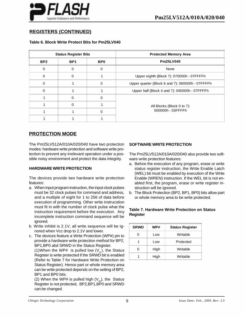
Status Register Bits Protected Memory Area
BP2 BP1 BP0 Pm25LV040
0 0 0 None
0 0 1 Upper eighth (Block 7): 070000h - 07FFFFh
0 1 0 Upper quarter (Block 6 and 7): 060000h - 07FFFFh
0 1 1 Upper half (Block 4 and 7): 040000h - 07FFFFh
1 0 0
All Blocks (Block 0 to 7):000000h - 03FFFFh
1 0 1
1 1 0
1 1 1
Table 6. Block Write Protect Bits for Pm25LV040
REGISTERS (CONTINUED)
PROTECTION MODE
The Pm25LV512A/010A/020/040 have two protectionmodes: hardware write protection and software write pro-tection to prevent any irrelevant operation under a pos-sible noisy environment and protect the data integrity.
HARDWARE WRITE PROTECTION
The devices provide two hardware write protectionfeatures:a. When input program instruction, the input clock pulses
must be 32 clock pulses for command and address,and a multiple of eight for 1 to 256 of data beforeexecution of programming. Other write instrucstionmust fit in with the number of clock pulse what theinstruction requirement before the execution. Anyincomplete instruction command sequence will beignored.
b. Write inhibit is 2.1V, all write sequence will be ig-nored when Vcc drop to 2.1V and lower.
c. The devices feature a Write Protection (WP#) pin toprovide a hardware write protection method for BP2,BP1,BP0 abd SRWD in the Status Register.(1)When the WP# is pulled low (V
IL), the Status
Register is write protected if the SRWD bit is enabled(Refer to Table 7 for Hardware Write Protection onStatus Register). Hence part or whole memory areacan be write protected depends on the setting of BP2,BP1 and BP0 bits.(2) When the WP# is pulled high (V
IH), the Status
Register is not protected, BP2,BP1,BP0 and SRWDcan be changed.
SOFTWARE WRITE PROTECTION
The Pm25LV512A/010A/020/040 also provide two soft-ware write protection features:a. Before the execution of any program, erase or write
status register instruction, the Write Enable Latch(WEL) bit must be enabled by execution of the WriteEnable (WREN) instruction. If the WEL bit is not en-abled first, the program, erase or write register in-struction will be ignored.
b. The Block Protection (BP2, BP1, BP0) bits allow partor whole memory area to be write protected.
SRWD WP# Status Register
0 Low Writable
1 Low Protected
0 High Writable
1 High Writable
Table 7. Hardware Write Protection on StatusRegister

10Chingis Technology Corporation Issue Date: Feb., 2009, Rev: 3.5
Pm25LV512A/010A/020/040
The Pm25LV512A/010A/020/040 utilize an 8-bit instruc-tion register. Refer to Table 8 Instruction Set for the de-tail Instructions and Instruction Codes. All instructions,addresses, and data are shifted in with the most signifi-cant bit (MSB) first on Serial Data Input (SI). The inputdata on SI is latched on the rising edge of Serial Clock(SCK) after the Chip Enable (CE#) is driven low (VIL).
Table 8. Instruction Set
DEVICE OPERATION
Every instruction sequence starts with a one-byte in-struction code and might be followed by address bytes,data bytes, or address bytes and data bytes dependson the type of instruction. The CE# must be driven high(VIH) after the last bit of the instruction sequence hasbeen shifted in.
HOLD OPERATION
The HOLD# is used in conjunction with the CE# to se-lect the Pm25LV512A/010A/020/040. When the devicesare selected and a serial sequence is underway, HOLD#can be used to pause the serial communication
with the master device without resetting the serialsequence. To pause, the HOLD# must be brought lowwhile the SCK signal is low. To resume serial communi-cation, the HOLD# is brought high while the SCK signalis low (SCK may still toggle during HOLD). Inputs to theSl will be ignored while the SO is in the high impedancestate.
Instruction Name Instruction Format Hex Code Operation
WREN 0000 0110 06h Write Enable
WRDI 0000 0100 04h Write Disable
RDSR 0000 0101 05h Read Status Register
WRSR 0000 0001 01h Write Status Register
READ 0000 0011 03h Read Data Bytes from Memory at Normal Read Mode
FAST_READ 0000 1011 0Bh Read Data Bytes from Memory at Fast Read Mode
RDID 1010 1011 ABh Read Manufacturer and Product ID
JEDEC ID READ*1 1001 1111 9Fh Read Manufacturer and Prduct ID by JEDEC ID Command
PAGE_ PROG 0000 0010 02h Page Program Data Bytes Into Memory
RDCR 1010 0001 A1h Read Configuration Register
WRCR 1111 0001 F1h Write Configuration Register
SECTOR_ER 1101 0111 D7h Sector Erase
BLOCK_ER 1101 1000 D8h Block Erase
CHIP_ER 1100 0111 C7h Chip Erase

11Chingis Technology Corporation Issue Date: Feb., 2009, Rev: 3.5
Pm25LV512A/010A/020/040
0 1 8 31 38 39 46 47 54
HIGH IMPEDANCEManufacture ID1 Device ID Manufacture ID2
S C K
CE#
SI
S O
INSTRUCTION
97
1010 1011b
3 Dummy Bytes
Figure 3. Read Product Identification Sequence
DEVICE OPERATION (CONTINUED)
Product Identification Data
Manufacturer IDFirst Byte 9Dh
Second Byte 7Fh
Device ID:
Pm25LV512A 7Bh
Pm25LV010A 7Ch
Pm25LV020 7Dh
Pm25LV040 7Eh
Table 9. Product IdentificationREAD PRODUCT IDENTIFICATION OPERATION
The Read Product Identification (RDID) instruction al-lows the user to read the manufacturer and product ID ofthe devices. Refer to Table 9 Product Identification forpFLASH™ manufacturer ID and device ID. The RDID in-struction code is followed by three dummy bytes, eachbit being latched-in on SI during the rising edge of SCK.Then the first manufacturer ID (9Dh) is shifted out on SOwith the MSB first, followed by the device ID and thesecond manufacturer ID (7Fh), each bit been shifted outduring the falling edge of SCK. If the CE# stays low afterthe last bit of second manufacturer ID is shifted out, themanufacturer ID and device ID will be looping until thepulled high of CE# signal.

12Chingis Technology Corporation Issue Date: Feb., 2009, Rev: 3.5
Pm25LV512A/010A/020/040
DEVICE OPERATION (CONTINUED)
READ PRODUCT IDENTIFICATION BY JEDEC IDCOMMAND
The JEDEC ID READ instruction allows the user to readthe manufacturer and product ID of the devices. Refer toTable 9 Product Identification for pFLASH™ manufac-turer ID and device ID. The second manufacturer ID (7Fh)is shifted out on SO with the MSB first after JEDEC IDREAD command input, followed by the first manufac-turer ID (9Dh) and the device ID, each bit been shiftedout during the falling edge of SCK.
If the CE# stays low after the last bit of device ID isshifted out, the manufacturer ID and device ID will be loop-ing until the pulled high of CE# signal.
Pm25LV512A do not support this JEDEC ID READinstruction.
Figure 4. Read Product Identification by JEDEC ID READ Sequence
SCK
CE#
SI
INSTRUCTION
1001 1111b
0 8 15 23 24 317 16
HIGH IMPEDANCESO Device IDManufacture ID1Manufacture ID2

13Chingis Technology Corporation Issue Date: Feb., 2009, Rev: 3.5
Pm25LV512A/010A/020/040
DEVICE OPERATION (CONTINUED)
WRITE ENABLE OPERATION
The Write Enable (WREN) instruction is used to set theWrite Enable Latch (WEL) bit. The WEL bit of thePm25LV512A/010A/020/040 are set as write disable stateafter power-up. The WEL bit must be write enabled be-fore any write operation includes sector, block and
WRITE DISABLE OPERATION
To protect the device against inadvertent writes, the WriteDisable (WRDI) instruction resets the WEL bit and dis-ables all write instructions. The WRDI instruction is not
SCK
SI
S O
INSTRUCTION = 0000 0110b
HI-Z
CE#
Figure 5. Write Enable Sequence
Figure 6. Write Disable Sequence
CE#
SCK
SI
S O
INSTRUCTION = 0000 0100b
HI-Z
chip erase, page program, write status register, and writeconfiguration register operations. The WEL bit will bereset back to write disable state automatically after thecompletion of a write operation. The WREN instructionis required before any above instruction is executed.
required after the execution of a write instruction. TheWEL will be automatically reset.
14Chingis Technology Corporation Issue Date: Feb., 2009, Rev: 3.5
Pm25LV512A/010A/020/040
DEVICE OPERATION (CONTINUED)
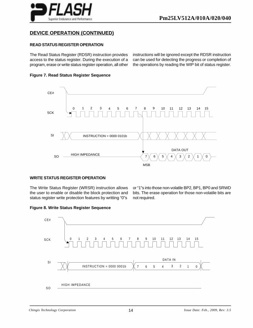
WRITE STATUS REGISTER OPERATION
The Write Status Register (WRSR) instruction allowsthe user to enable or disable the block protection andstatus register write protection features by writting “0”s
0 1 2 3 5 6 7 8 9 10 11 12 13 144 15
7 6 5 4 3 2 1 0
DATA IN
INSTRUCTION = 0000 0001b
HIGH IMPEDANCE
CE#
SCK
SI
S O
Figure 8. Write Status Register Sequence
or “1”s into those non-volatile BP2, BP1, BP0 and SRWDbits. The erase operation for those non-volatile bits arenot required.
READ STATUS REGISTER OPERATION
The Read Status Register (RDSR) instruction providesaccess to the status register. During the execution of aprogram, erase or write status register operation, all other
Figure 7. Read Status Register Sequence
CE#
SCK
SI
0 1 2 3 5 6 7 8 9 10 11 12 13 144
INSTRUCTION = 0000 0101b
SO 7 6 5 4 3 2 1 0HIGH IMPEDANCEDATA OUT
MSB
15
instructions will be ignored except the RDSR instructioncan be used for detecting the progress or completion ofthe operations by reading the WIP bit of status register.

15Chingis Technology Corporation Issue Date: Feb., 2009, Rev: 3.5
Pm25LV512A/010A/020/040
DEVICE OPERATION (CONTINUED)
0 1 2 3 5 6 7 8 9 10 11 12 13 144 15
7 6 5 4 3 2 1 0
DATA IN
INSTRUCTION = 1111 0001b
HIGH IMPEDANCE
CE#
SCK
SI
S O
Figure 10. Write Configuration Register Sequence
The Read Configuration Register (RDCR) instruction pro-vides access to the Configuration Register. This instruc-tion can be used to verify the configuration setting of
Figure 9. Read Configuration Register Sequence
CE#
SCK
SI
0 1 2 3 5 6 7 8 9 10 11 12 13 144
INSTRUCTION = 1010 0001b
SO 7 6 5 4 3 2 1 0HIGH IMPEDANCEDATA OUT
MSB
15
bottom Sector 0 and the write protection setting for eachindividual 1 Kbyte sector (Sector 0_0 ~ Sector 0_3) withinthe Sector 0.
READ CONFIGURATION REGISTER OPERATION
WRITE CONFIGURATION REGISTER OPERATION
The Write Configuration Register (WRCR) instruction al-lows user to enable or disable four smaller 1K bytesectors and protection for each 1K byte sector by writ-ing “0”s or “1”s into SCFG and SP0_3 ~SP0_1 in thecongiguration register. please refer table 2 for details.
Do not require WREN command before this WRCRoperation. Because Configuration Register is a data latcharchitecture.

16Chingis Technology Corporation Issue Date: Feb., 2009, Rev: 3.5
Pm25LV512A/010A/020/040
READ DATA OPERATION
The Read Data (READ) instruction is used to read memorydata of Pm25LV512A/010A/020/040 under normal moderunning up to 33 MHz.
The READ instruction is activated by pulling the CE#line of the selected device to low (VIL), and the READinstruction code is transmitted via the Sl line followed bythree bytes address (A23 - A0) to be read. There aretotal 24 address bits will be shifted in, only the AMS (most-significant address) - A0 will be decoded and the rest ofA23 - AMS can be don’t cared. Refer to Table 10 for therelated Address Key. Upon completion, any data on theSl will be ignored.
Figure 11. Read Data Sequence
0 1 2 3 4 5 6 7 8 9 10 11 28 29 30 31 32 33 34 3635 37 38
...23 22 21 3 2 1 0
7 6 5 4 3 2 1 0
3-BYTE ADDRESS
INSTRUCTION = 0000 0011b
HIGH IMPEDANCE
CE#
SCK
SI
SO
39
Address Pm25LV512A Pm25LV010A Pm25LV020 Pm25LV040
AN A15 - A0 A16 - A0 A17 - A0 A18 - A0
Don't Care Bits A23 - A16 A23 - A17 A23 - A18 A23 - A19
Table 10. Address Key
The first byte data D7 - D0 addressed (can be at anylocation) is then shifted out onto the SO line. A singlebyte data or up to whole memory array can be read outin one READ instruction. The address is automaticallyincreamented to the next higher address after each byteof data is shifted out. The read operation can be termi-nated any time by driving the CE# high (VIH) after thedata comes out. When the highest address of the de-vices is reached, the address counter will roll over to the000000h address allowing the entire memory to be readin one continuous READ instruction.
DEVICE OPERATION (CONTINUED)

17Chingis Technology Corporation Issue Date: Feb., 2009, Rev: 3.5
Pm25LV512A/010A/020/040
FAST READ DATA OPERATION
The Pm25LV512A/010A/020/040 also feature a FastRead (FAST_READ) instruction. This FAST_READ in-struction is used to read memory data in 100 MHz clockrate where the FAST_READ instruction proceeding.
The devices are first selected by driving CE# low (VIL).The FAST_READ instruction code followed by three bytesaddress (A23 - A0) and a dummy byte (8 clocks) istrasmitted via the SI line, each bit being latched-in dur-ing the rising edge of SCK. Then the first data byte
DEVICE OPERATION (CONTINUED)
Figure 12. Fast Read Data Sequence
0 1 2 3 4 5 6 7 8 9 10 11 28 29 30 31
...23 22 21 3 2 1 0
3-BYTE ADDRESS
INSTRUCTION = 0000 1011b
HIGH IMPEDANCE
CE#
SCK
SI
S O
addressed is shifted out on SO line, each bit being shiftedout at a maximum frequency fCT, during the falling edgeof SCK.
The first byte addressed can be at any location. Theaddress is automatically incremented to the next higheraddress after each byte of data is shifted out. When thehighest address is reached, the address counter will rollover to the 000000h address allowing the entire memoryto be read with a single FAST_READ instruction. TheFAST_READ instruction is terminated by driving CE#high (VIH).
32 33 34 35 36 37 38 39 40 41 42 43 44 45 46 47
7 6 5 3 0
7 6 5 4 3 2 1 0HIGH IMPEDANCE
CE#
SCK
SI
SO
4 1
7 6 5 4 3 2 1 0
2
DATA OUT 1 DATA OUT 2
DUMMY BYTE
48
18Chingis Technology Corporation Issue Date: Feb., 2009, Rev: 3.5
Pm25LV512A/010A/020/040
DEVICE OPERATION (CONTINUED)
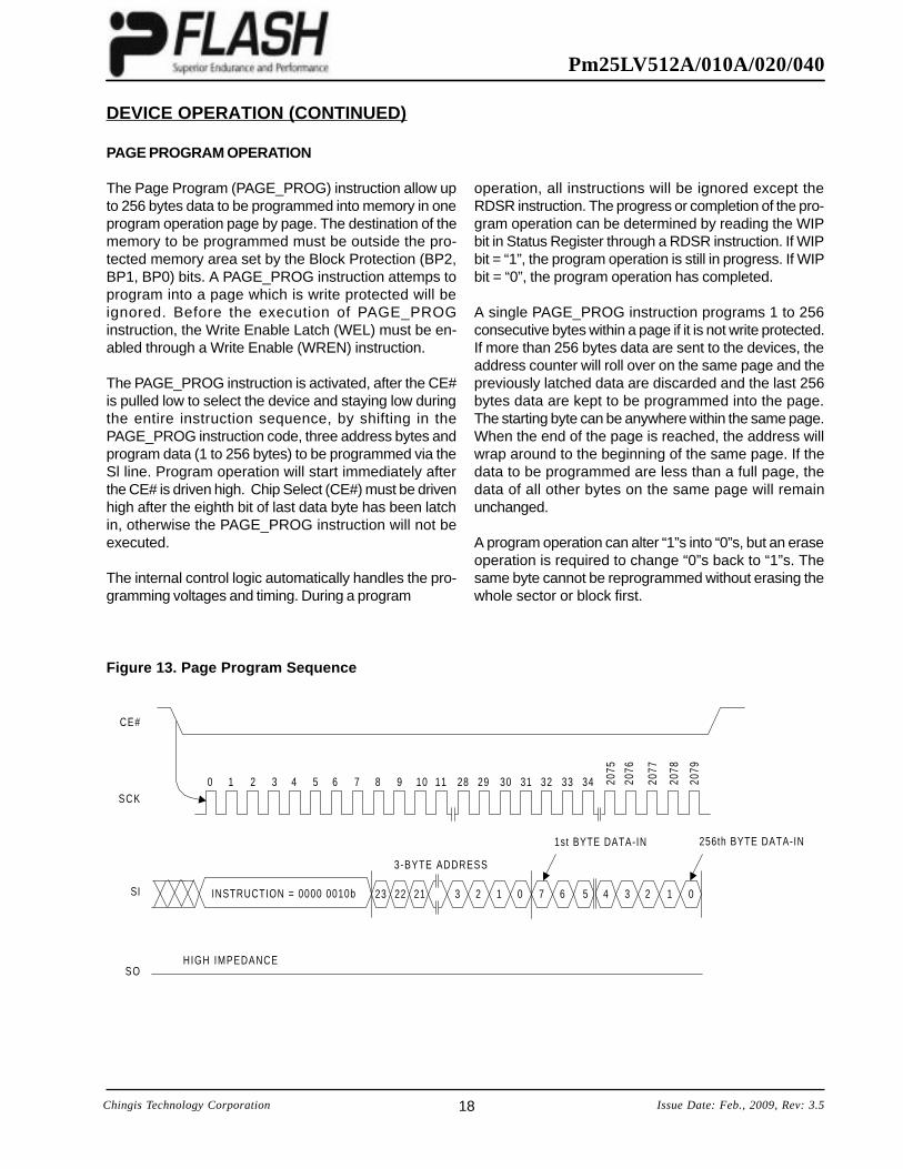
PAGE PROGRAM OPERATION
The Page Program (PAGE_PROG) instruction allow upto 256 bytes data to be programmed into memory in oneprogram operation page by page. The destination of thememory to be programmed must be outside the pro-tected memory area set by the Block Protection (BP2,BP1, BP0) bits. A PAGE_PROG instruction attemps toprogram into a page which is write protected will beignored. Before the execution of PAGE_PROGinstruction, the Write Enable Latch (WEL) must be en-abled through a Write Enable (WREN) instruction.
The PAGE_PROG instruction is activated, after the CE#is pulled low to select the device and staying low duringthe entire instruction sequence, by shifting in thePAGE_PROG instruction code, three address bytes andprogram data (1 to 256 bytes) to be programmed via theSl line. Program operation will start immediately afterthe CE# is driven high. Chip Select (CE#) must be drivenhigh after the eighth bit of last data byte has been latchin, otherwise the PAGE_PROG instruction will not beexecuted.
The internal control logic automatically handles the pro-gramming voltages and timing. During a program
operation, all instructions will be ignored except theRDSR instruction. The progress or completion of the pro-gram operation can be determined by reading the WIPbit in Status Register through a RDSR instruction. If WIPbit = “1”, the program operation is still in progress. If WIPbit = “0”, the program operation has completed.
A single PAGE_PROG instruction programs 1 to 256consecutive bytes within a page if it is not write protected.If more than 256 bytes data are sent to the devices, theaddress counter will roll over on the same page and thepreviously latched data are discarded and the last 256bytes data are kept to be programmed into the page.The starting byte can be anywhere within the same page.When the end of the page is reached, the address willwrap around to the beginning of the same page. If thedata to be programmed are less than a full page, thedata of all other bytes on the same page will remainunchanged.
A program operation can alter “1”s into “0”s, but an eraseoperation is required to change “0”s back to “1”s. Thesame byte cannot be reprogrammed without erasing thewhole sector or block first.
Figure 13. Page Program Sequence
0 1 2 3 4 5 6 7 8 9 10 11 28 29 30 31 32 33 34 2075
2076
2077
2078
2079
0 7 6 53 2 2 11 4 3 023 22 21
1st BYTE DATA-IN 256th BYTE DATA-IN
3-BYTE ADDRESS
INSTRUCTION = 0000 0010b
HIGH IMPEDANCE
CE#
SCK
SI
SO

19Chingis Technology Corporation Issue Date: Feb., 2009, Rev: 3.5
Pm25LV512A/010A/020/040
ERASE OPERATION
The memory array of Pm25LV512A/010A is organizedinto uniform 4 Kbyte sectors or 32 Kbyte uniform blocks(sector group - consists of eight adjacent sectors). Thememory array of Pm25LV020/040 are organized intouniform 4 Kbyte sectors or 64 Kbyte uniform blocks (sec-tor group - consists of sixteen adjacent sectors). ThePm25LV010A/020/040 of bottom sector (Sector 0) of thedevices can be configured into four 1 Kbyte smallersectors.
Before a byte can be reprogrammed, the sector or blockwhich contains this byte must be erased first. In order toerase the devices, there are three erase instructions in-clude Sector Erase (SECTOR_ER), Block Erase(BLOCK_ER) and Chip Erase (CHIP_ER) instructionscan be used. A sector erase operation allows to eraseany individual sector without affecting the data in others.A block erase operation allows to erase any individualblock. And a chip erase operation allows to erase thewhole memory array of the devices. Pre-programs thedevices are not required prior to a sector erase, blockerase or chip erase operation.
SECTOR ERASE OPERATION
A SECTOR_ER instruction erases a 4 Kbyte sector or a1 Kbyte smaller sector (Sector 0_3, Sector 0_2, Sector0_1, Sector 0_0) if the bottom Sector 0 has been config-ured as four smaller sectors. Before the execution ofSECTOR_ER instruction, the Write Enable Latch (WEL)must be enabled through a Write Enable (WREN) instruc-tion. The WEL will be reset automatically after thecompletion of sector erase operation.
The SECTOR_ER instruction is entered, after the CE#is pulled low to select the device and staying low duringthe entire instruction sequence, by shifting in theSECTOR_ER instruction code and three address bytesvia the SI. Erase operation will start immediately afterthe CE# is pulled high, otherwise the SECTOR_ER in-struction will not be executed. The internal control logicautomatically handles the erase voltage and timing. Re-fer to Figure 13 for Sector Erase Sequence.
During a erase operation, all instruction will be ignoredexcept the Read Status Register (RDSR) instruction.The progress or completion of the erase opertion can bedetermined by reading the WIP bit in Status Registerthrough a RDSR instruction. If WIP bit = “1”, the eraseoperation is still in progress. If WIP bit = “0”, the eraseoperation has been completed.
DEVICE OPERATION (CONTINUED)
BLOCK ERASE OPERATION
A Block Erase (BLOCK_ER) instruction erases a 32Kbyte block for the Pm25LV512A/010A or a 64 Kbyteblock for the Pm25LV020/040. Before the execution ofBLOCK_ER instruction, the Write Enable Latch (WEL)must be enabled through a Write Enable (WREN) instruc-tion. The WEL will be reset automatically after thecompletion of block erase operation.
The BLOCK_ER instruction is entered, after the CE# ispulled low to select the device and staying low duringthe entire instruction sequence, by shifting in theBLOCK_ER instruction code and three address bytesvia the SI. Erase operation will start immediately afterthe CE# is pulled high, otherwise the BLOCK_ER in-struction will not be executed. The internal control logicautomatically handles the erase voltage and timing. Re-fer to Figure 14 for Block Erase Sequence.
CHIP ERASE OPERATION
A Chip Erase (CHIP_ER) instruction erases the wholememory array of Pm25LV512A/010A/020/040. Before theexecution of CHIP_ER instruction, the Write Enable Latch(WEL) must be enabled through a Write Enable (WREN)instruction. The WEL will be reset automatically afterthe completion of chip erase operation.
The CHIP_ER instruction is entered, after the CE# ispulled low to select the device and staying low duringthe entire instruction sequence, by shifting in theCHIP_ER instruction code via the SI. Erase operationwill start immediately after the CE# is pulled high, other-wise the CHIP_ER instruction will not be executed. Theinternal control logic automatically handles the erasevoltage and timing. Refer to Figure 15 for Chip EraseSequence.

20Chingis Technology Corporation Issue Date: Feb., 2009, Rev: 3.5
Pm25LV512A/010A/020/040
Figure 15. Block Erase Sequence
Figure 16. Chip Erase Sequence
0 1 2 3 4 5 6 7 8 9 10 11 28 29 30 31
0123212223 ...3-BYTE ADDRESS
INSTRUCTION = 1101 1000b
HIGH IMPEDANCE
CE#
SCK
SI
S O
0 1 2 3 4 5 6 7
HIGH IMPEDANCE
S C K
CE#
SI
S O
INSTRUCTION = 1100 0111b
0 1 2 3 4 5 6 7 8 9 10 11 28 29 30 31
0123212223 ...3-BYTE ADDRESS
INSTRUCTION = 1101 0111b
HIGH IMPEDANCE
CE#
SCK
SI
S O
Figure 14. Sector Erase Sequence
DEVICE OPERATION (CONTINUED)

21Chingis Technology Corporation Issue Date: Feb., 2009, Rev: 3.5
Pm25LV512A/010A/020/040
Table 11. Block/Sector Addresses of Pm25LV512A/010A
Note: 1. Pm25LV010A support 1KByte small sector - Sector 0 can be configured into four smaller 1 Kbytesectors (Sector 0_0: 000000h - 0003FFh, Sector 0_1: 000400h - 0007FFh, Sector 0_2: 000800h -000BFFh, and Sector 0_3: 000C00h - 000FFFh).
BLOCK/SECTOR ADDRESS
Block No.Block Size(Kbytes)
Sector No.Sector Size
(Kbytes)Address Range
Sector 0(1) 4 000000h - 000FFFh
Sector 1 4 001000h - 001FFFh
: : :
Sector 7 4 007000h - 007FFFh
Sector 8 4 008000h - 008FFFh
Sector 9 4 009000h - 009FFFh
: : 000000h - 006FFFh
Sector 15 4 00F000h - 00FFFFh
Block 2 32 " " 010000h - 017FFFh
Block 3 32 " " 018000h - 01FFFFh
Memory Density
1 Mbit
512 Kbit
32
32
Block 0
Block 1

22Chingis Technology Corporation Issue Date: Feb., 2009, Rev: 3.5
Pm25LV512A/010A/020/040
Table 12. Block/Sector Addresses of Pm25LV020/040
Memory Density Block No. Block Size(Kbytes) Sector No. Sector Size
(Kbytes) Address Range
2 Mbit
4 Mbit
Block 0 64
Sector 0 (1) 4 000000h - 000FFFh
Sector 1 4 001000h - 001FFFh
: : :
Sector 15 4 00F000h - 00FFFFh
Block 1 64
Sector 16 4 010000h - 010FFFh
Sector 17 4 011000h - 011FFFh
: : :
Sector 31 4 01F000h - 01FFFFh
Block 2 64 " " 020000h - 02FFFFh
Block 3 64 " " 030000h - 03FFFFh
Block 4 64 " " 040000h - 04FFFFh
Block 5 64 " " 050000h - 05FFFFh
Block 6 64 " " 060000h - 06FFFFh
Block 7 64 " " 070000h - 07FFFFh
Note: 1. Sector 0 can be configured into four smaller 1 Kbyte sectors (Sector 0_0: 000000h - 0003FFh, Sector0_1: 000400h - 0007FFh, Sector 0_2: 000800h - 000BFFh, and Sector 0_3: 000C00h - 000FFFh).
BLOCK/SECTOR ADDRESS (CONTINUED)

23Chingis Technology Corporation Issue Date: Feb., 2009, Rev: 3.5
Pm25LV512A/010A/020/040
DC AND AC OPERATING RANGE
ABSOLUTE MAXIMUM RA TINGS (1)
Notes:1. Stresses under those listed in “Absolute Maximum Ratings” may cause permanent damage
to the device. This is a stress rating only. The functional operation of the device or any otherconditions under those indicated in the operational sections of this specification is notimplied. Exposure to absolute maximum rating condition for extended periods may affecteddevice reliability.
2. Maximum DC voltage on input or I/O pins are VCC + 0.5 V. During voltage transitioningperiod, input or I/O pins may overshoot to VCC + 2.0 V for a period of time up to 20 ns.Minimum DC voltage on input or I/O pins are -0.5 V. During voltage transitioning period,input or I/O pins may undershoot GND to -2.0 V for a period of time up to 20 ns.
Temperature Under Bias -65oC to +125oC
Storage Temperature -65oC to +125oC
Surface Mount Lead Soldering TemperatureStandard Package 240oC 3 Seconds
Lead-free Package 260oC 3 Seconds
Input Voltage with Respect to Ground on All Pins (2) -0.5 V to VCC + 0.5 V
All Output Voltage with Respect to Ground -0.5 V to VCC + 0.5 V
VCC (2) -0.5 V to +6.0 V
Part Number Pm25LV512A/010A/020/040
Operating Temperature -40oC to +105oC
Vcc Power Supply 2.7 V - 3.6 V

24Chingis Technology Corporation Issue Date: Feb., 2009, Rev: 3.5
Pm25LV512A/010A/020/040
DC CHARACTERISTICS
Applicable over recommended operating range from:T
AC = -40°C to +105°C, V
CC = 2.7 V to 3.6 V (unless otherwise noted).
Symbol Parameter Min Typ Max Units
ICC1 Vcc Active Read Current 10 15 mA
ICC2 Vcc Program/Erase Current 15 30 mA
ISB1 Vcc Standby Current CMOS 10 20 uA
ISB2 Vcc Standby Current TTL 3 mA
ILI Input Leakage Current 1 uA
ILO Output Leakage Current 1 uA
VIL Input Low Voltage -0.5 0.8 V
VIH Input HIgh Voltage 0.7VCC VCC + 0.3 V
VOL Output Low Voltage IOL = 2.1 mA 0.45 V
VOH Output High Voltage IOH = -100 uA VCC - 0.2 V2.7V < VCC < 3.6V
VCC = 3.6V, CE# = VIH to VCC
VIN = 0V to VCC
VIN = 0V to VCC, TAC = 0oC to 105oC
Condition
VCC = 3.6V at 33 MHz, SO = Open
VCC = 3.6V at 33 MHz, SO = Open
VCC = 3.6V, CE# = VCC

25Chingis Technology Corporation Issue Date: Feb., 2009, Rev: 3.5
Pm25LV512A/010A/020/040
AC CHARACTERISTICS
Applicable over recommended operating range from TA = -40°C to +105°C, V
CC = 2.7 V to 3.6 V
CL = 1TTL Gate and 10 pF (unless otherwise noted).
Symbol Parameter Min Typ Max Units
fCT Clock Frequency for fast read mode 0 100 MHz
fC Clock Frequency for read mode 0 33 MHz
tRI Input Rise Time 8 ns
tFI Input Fall Time 8 ns
tCKH SCK High Time 4 ns
tCKL SCK Low Time 4 ns
tCEH CE# High Time 25 ns
tCS CE# Setup Time 10 ns
tCH CE# Hold Time 5 ns
tDS Data In Setup Time 2 ns
tDH Data in Hold Time 2 ns
tHS Hold Setup Time 15 ns
tHD Hold Time 15 ns
tV Output Valid 8 ns
tOH Output Hold Time Normal Mode 0 ns
tLZ Hold to Output Low Z 200 ns
tHZ Hold to Output High Z 200 ns
tDIS Output Disable Time 100 ns
tEC Secter/Block/Chip Erase Time 60 100 ms
tPP Page Program Time 2 5 ms
tW Write Status Register Time 60 100 ms
tVCS VCC Set-up Time 50 µs
26Chingis Technology Corporation Issue Date: Feb., 2009, Rev: 3.5
Pm25LV512A/010A/020/040
AC CHARACTERISTICS (CONTINUED)
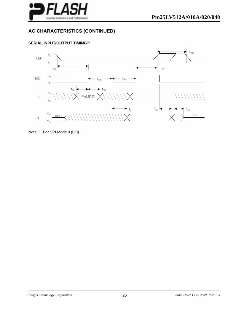
SERIAL INPUT/OUTPUT TIMING(1)
Note: 1. For SPI Mode 0 (0,0)
VALID IN
CE#
VIL
VIH
SCKV
IH
VIH
VOH
VIL
VIL
VOL
SI
SO
tCS
tCKH
tCKL
tCEH
tDH
tDS
tV
tDIS
tOH
HI-ZHI-Z
tCH

27Chingis Technology Corporation Issue Date: Feb., 2009, Rev: 3.5
Pm25LV512A/010A/020/040
AC CHARACTERISTICS (CONTINUED)
tH DtH D
tH S
tH S
tH Z
tL Z
CE#
SCK
HOLD#
S O
HOLD TIMING
Typ Max Units Conditions
CIN 4 6 pF VIN = 0 V
COUT 8 12 pF VOUT = 0 V
PIN CAPACITANCE ( f = 1 MHz, T = 25°C )
Note: These parameters are characterized but not 100% tested.
OUTPUT TEST LOAD INPUT TEST WAVEFORMS
AND MEASUREMENT LEVEL
Vcc
1.8 K
1.3 K
OUTPUT PIN
10 pF
0.8Vcc
0.2Vcc
0.5 VccACMeasurementLevel
Input
Note: 1. Input Pulse Voltage : 0.2Vcc to 0.8Vcc. 2. Input Timing Reference Voltages : 0.3Vcc to 0.7Vcc. 3. Output Timing Reference Voltage : Vcc/2.

28Chingis Technology Corporation Issue Date: Feb., 2009, Rev: 3.5
Pm25LV512A/010A/020/040
POWER-UP AND POWER-DOWN
At Power-up and Power-down, the device must not beselected (CE# must follow the voltage applied on Vcc)until Vcc reaches the correct value:- Vcc(min) at Power-up, and then for a further delay of tVCE- Vss at Power-downUsually a simple pull-up resistor on CE# can be used toinsure safe and proper Power-up and Power-down.To avoid data corruption and inadvertent write operationsduring power up, a Power On Reset (POR) circuit isincluded. The logic inside the device is held reset whileVcc is less than the POR threshold value (Vwi) duringpower up, the device does not respond to any instructionuntil a time delay of tPUW has elapsed after the momentthat Vcc rised above the VWI threshold. However, thecorrect operation of the device is not guaranteed if, bythis time, Vcc is still below Vcc(min). No Write Status
Chip Selection Not Allowed
All Write Commands are Rejected
tVCE Read Access Allowed Device fully accessible
tPUW
Vcc
Vcc(max)
Vcc(min)Reset State
V (write inhibit)
Time
Symbol Parameter Min. Max. UnittVCE
*1 Vcc(min) to CE# Low 10 us
tPUW *1 Power-Up time delay to Write instruction 1 10 ms
VWI*1 Write Inhibit Voltage 2.1 2.3 V
Note : *1. These parameters are characterized only.
Power-up Timing
Register, Program or Erase instructions should be sentuntil the later of:- tPUW after Vcc passed the VWI threshold- tVCE after Vcc passed the Vcc(min) level
At Power-up, the device is in the following state:- The device is in the Standby mode- The Write Enable Latch (WEL) bit is reset
At Power-down, when Vcc drops from the operatingvoltage, to below the Vwi, all write operations are dis-abled and the device does not respond to any writeinstruction.

29Chingis Technology Corporation Issue Date: Feb., 2009, Rev: 3.5
Pm25LV512A/010A/020/040
PROGRAM/ERASE PERFORMANCE
Parameter Unit Typ Max Remarks
Sector Erase Time ms 60 100 From writing erase command to erase completion
Block Erase Time ms 60 100 From writing erase command to erase completion
Chip Erase Time ms 60 100 From writing erase command to erase completion
Page Programming Time ms 2 5From writing program command to programcompletion
Parameter Min Typ Unit Test Method
Endurance 200,000 Cycles JEDEC Standard A117
Data Retention 20 Years JEDEC Standard A103
ESD - Human Body Model 2,000 Volts JEDEC Standard A114
ESD - Machine Model 200 Volts JEDEC Standard A115
ESD - Charged Device Model 1,000 Volts JEDEC Standard C101-A
Latch-Up 100 + ICC1 mA JEDEC Standard 78
Note: These parameters are characterized and are not 100% tested.
Note: These parameters are characterized and are not 100% tested.
RELIABILITY CHARACTERISTICS
30Chingis Technology Corporation Issue Date: Feb., 2009, Rev: 3.5
Pm25LV512A/010A/020/040
PACKAGE TYPE INFORMA TION
`
End View
5.004.80
Top View Side View
4.003.80
6.205.80
1.751.35
0.250.10
0.510.33
1.27 BSC
0.250.19
1.270.40
45º
8o0o
0.5950.495
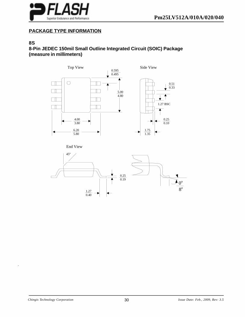
8S8-Pin JEDEC 150mil Small Outline Integrated Circuit (SOIC) Package(measure in millimeters)

31Chingis Technology Corporation Issue Date: Feb., 2009, Rev: 3.5
Pm25LV512A/010A/020/040
PACKAGE TYPE INFORMA TION
`
End View
5.385.18
Top View Side View
5.385.18
8.107.70
2.161.75
0.250.05
0.480.35
1.27 BSC
0.250.19
0.800.50
5.385.18
5.335.13
8B8-Pin JEDEC 208mil Broad Small Outline Integrated Circuit (SOIC) Package(measure in millimeters)

32Chingis Technology Corporation Issue Date: Feb., 2009, Rev: 3.5
Pm25LV512A/010A/020/040
PACKAGE TYPE INFORMA TION (CONTINUED)
8K8-Contact Ulta-Thin Small Outline No-Lead (WSON) Package (measure in millimeters)
5.00BSC
Top View Side View
0.480.35
6.00BSC
0.800.70
0.250.19
1.27BSC
Bottom ViewPin 1
0.750.50
4.00
3.40

33Chingis Technology Corporation Issue Date: Feb., 2009, Rev: 3.5
Pm25LV512A/010A/020/040
PACKAGE TYPE INFORMA TION (CONTINUED)
8P8-pin 300mil wide body, Plastic Dual In-Line Package PDIP (measure in millimeters)
9.539.12
6.606.20
9.408.38
0o
15o
3.453.25
0.38(min)
2.54(typ)
8.267.62
4.203.60
3.18(min)
1.651.40
0.560.36
34Chingis Technology Corporation Issue Date: Feb., 2009, Rev: 3.5
Pm25LV512A/010A/020/040
PACKAGE TYPE INFORMA TION (CONTINUED)
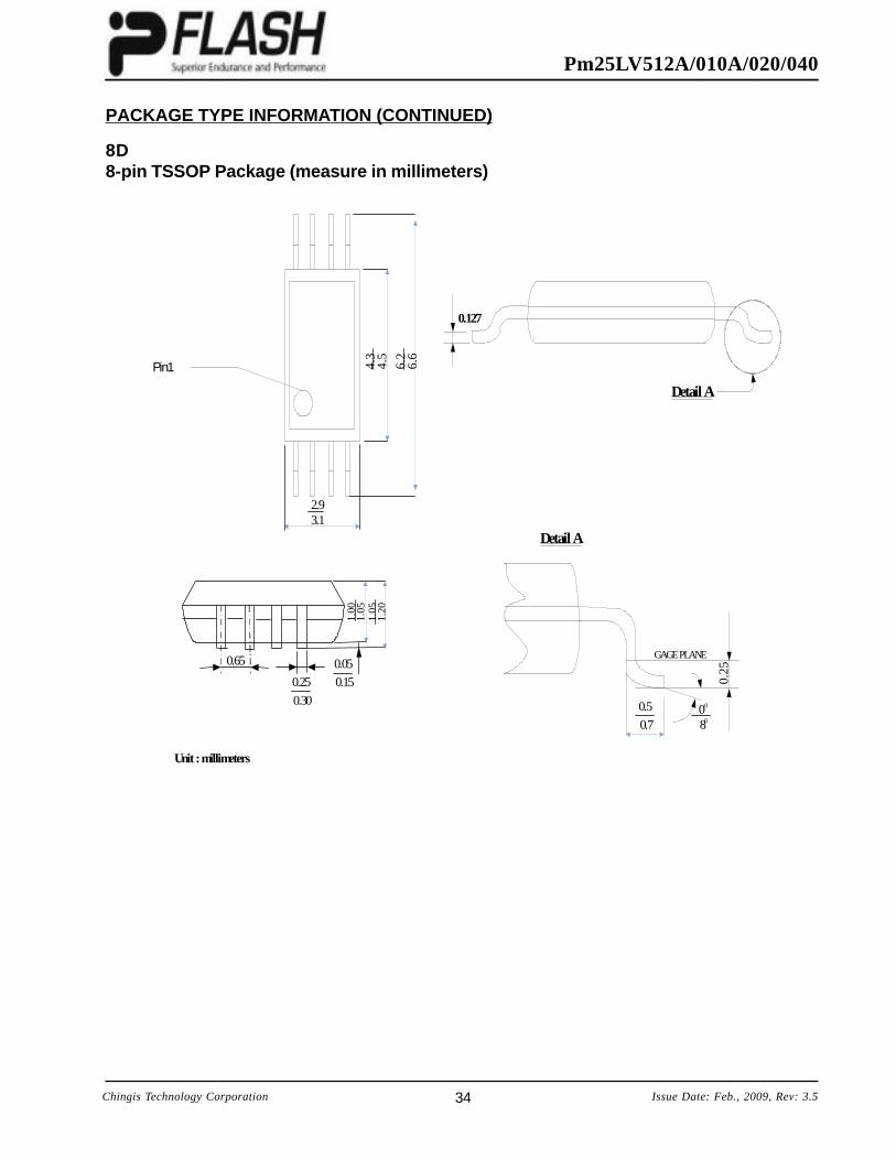
8D8-pin TSSOP Package (measure in millimeters)
Pin1 4.5
0.65
4.3
6.6
6.2
3.12.9
0.30
0.25
1.05
1.00
1.05
1.20
0.15
0.05
800
00.7
0.50.
25
GAGE PLANE
Detail A
Detail A
0.127
Unit : millimeters
35Chingis Technology Corporation Issue Date: Feb., 2009, Rev: 3.5
Pm25LV512A/010A/020/040
REVISION HISTORY
D ate R ev is io n N o . D escrip tio n o f C h an g es P ag e N o .
January, 2004 0 .3 A dvanced P roduct S pecifica tion A ll
M arch, 2004 0 .4 E xtend The Range o f Opera tion Tem pera ture A ll
A ugust, 2004 0 .5C orrect pa rt no fo r W S ON packageReg iste r sta tus se tting
36 ,7 ,8
October, 2004 0 .6C orrect pa rt noReg is te r se tting fo r sm a ll secto r fea thure
A llpage 7
January, 2005 0 .7 P re lim inary ve rs ion re lease
January, 2005 0 .81 . S upport 208m il S OIC package2 . C orrect read tim ing fo r D 0 la tch by HOS T3. Rem ove Turbo m ode
A ll
F ebruary, 2005 0 .9S upport 33M HzRem oved bask s ide m eta l o f W S ONS tandby current
1 ,3 ,15 ,23 ,24 ,30
M ay, 2005 1 .0JE D E C ID RE A D instructionC orrect the sm a lle r secto r (1K B ) fea ture
6 ,7 ,10 ,12
June , 2005 1 .1D escrip tion upda te fo r the opera tion o f C onfigura tionReg is te r
8 ,9 ,15 ,16
July, 2005 2 .0 S upport 75M Hz fo r F ast Read M ode A ll
July, 2005 2 .1
1 . Upda te fast read speed to 100MHz.2 . S ecto re /B lock a rche ticture descrip tion.3 . Ordering info rm ation - remove non-pb free parts .4 . Highligh no require W RE N be fo re W RC R com m and.5 . A C measurement cond itions.
1 ,3 ,16 ,28
Novem ber, 2005 2 .3
1 . C hange A C param ate rs fo r 100MHz spec. Tv 8ns with 10pF Load ing , D a ta In Ho ld /S e tup ti im e 2ns(m in), C lock high/low tim e 4ns(m in) TRI, TF I, 8ns(m ax), TD IS 10ns(m ax)2 . S upport C om m ercia l Grade to -40~+85degreeC3. P artno chage fo r P m 25LV 010 to P m 25LV 010A .
3 , 24 ,25
F ebruary, 2006 2 .41 . Upda te endurance to 200K cycle .2 . Upda te write inhib it spec. to 2 .1V .3 . Upda te E S D C D M spec 1000V.
1 ,9 ,28
M arch, 2006 2 .51 .C hange Logo and com pany nam e2.M od ified test cond ition fo r D C
A ll24
M arch, 2006 2 .6 E xtend the opera ted tem pera ture to +105degreeC 3,23 ,24 ,25
A pril, 2006 2 .71 . Upda te P m 25LV 512A in the da tashee t2 . C orrect tC H de finition3 . P ower-up tim ing d ifinition
A ll25 ,26
28
M ay, 2006 2 .8 C orrect the s ta tement o f ha rdware write p ro tection 9
June , 2006 2 .9 S upport 8 -p in P D IP package fo r 4Mb S P I 1 ,2 ,3 ,33
M ay, 2007 3 .0S upport secto r lock/unlock fea turesUpdate e rase and W RS R tim e
1,10 ,111 ,26 ,30
Jan. 2008 3 .1S upport TS S OP package fo r P m 25LV 512A .S upport S ecto r Lock/Unlock fo r P m 25LV 020.
1 , 3 ,3510 ,11
F eb. 2008 3 .2 S upport W S ON with back s ide m eta l 3 , 34

36Chingis Technology Corporation Issue Date: Feb., 2009, Rev: 3.5
Pm25LV512A/010A/020/040D a t e R e v i s i o n N o . D e s c r i p t i o n o f C h a n g e s P a g e N o .
J u n , 2 0 0 8 3 .3 A d d t h e T S S O P p a r t n u m b er 3
J u l y ,2 0 0 8 3 .4 R e m o v e 8 Q p a c k a g e 3
F e b , 2 0 0 9 3 .5 M o d if y D C C H Z t a b l e 2 4


 SPI Library A software defined, industry-standard, ... the application can connect via an interface connection using the spi_master_if](https://img.pdfslide.us/doc/110x75/5ae941467f8b9a36698b62b3/spi-library-xmos-userguide302rc1spi-302-spi-library-a-software-dened.jpg)