Embed Size (px)
Citation preview
Sequential Circuits:
Basic Concept

Fall 2019 Fundamentals of Digital Systems Design by Todor Stefanov, Leiden University
Overview
Sequential Circuits
Sequential vs. Combinational Circuits
Types of Sequential Circuits
Synchronous vs. Asynchronous Circuits
Sequential Circuit Representations
Boolean Equations
Characteristic (Flip-Flop Input) Equations
Primary Output Equations
State Table
State Diagram
Finite State Machines
Mealy vs. Moore Machines 2

Fall 2019 Fundamentals of Digital Systems Design by Todor Stefanov, Leiden University
Combinational vs. Sequential Circuits
Combinational circuits are memory-less and do not have feed-back loops. Thus, the output values depend ONLY on the current input values.
Able to perform useful operations (add, subtract, multiply, encode, decode, multiplex, demultiplex, etc…).
However, the performance of useful sequences of operations using only combinational circuits requires cascading many structures together.
Thus, the hardware to do this is very costly and inflexible.
To perform useful or flexible sequences of operations, we need to construct circuits that can store information between the operations.
Such circuits are called Sequential Circuits.
Combinational
Circuit n-inputs m-outputs n m
3

Fall 2019 Fundamentals of Digital Systems Design by Todor Stefanov, Leiden University
Sequential Circuits
Sequential circuits consist of combinational logic as well as
memory elements (used to store certain circuit states).
Outputs depend on BOTH current input values and previous
input values (kept in the storage elements).
There is a feed-back loop in the sequential circuits.
The storage elements are circuits that are capable of storing
binary information.
One storage element can store one bit of information.
n m
Combinational
Circuit
n-inputs m-outputs
Storage Elements Next
state Present state
q
feed-back loop
q
4

Fall 2019 Fundamentals of Digital Systems Design by Todor Stefanov, Leiden University
Storage Elements
Two types of storage elements are used in Sequential
Circuits: Latches and Flip-Flops.
Latches (D, SR,JK, T)
General description of a latch:
1-bit storage device with several inputs (X) and an output (Q).
Output is changed Q = f( X ) only when specific combinations occur
at the inputs X; otherwise the output remains unchanged (storage
mode).
Flip-Flops (D, SR,JK, T)
General description of a Flip-Flop:
1-bit storage device with several inputs (X), an output (Q), and a
specific trigger input (CLK).
Output is changed Q = f( X ) on response of a pulse at the trigger
input CLK (on the rising or falling edge of the pulse). When a pulse is
absent at input CLK the output remains unchanged (storage mode).
More details about Latches and Flip-Flops later!
L : X Q
FF : X
Q CLK
5

Fall 2019 Fundamentals of Digital Systems Design by Todor Stefanov, Leiden University
Types of Sequential Circuits
Sequential circuits are divided into two main types
depending on the storage elements that are used in
the feed-back loop.
Synchronous Sequential Circuits
Circuits with Flip-Flops in the feedback loop
Asynchronous Sequential Circuits
Circuits without storage elements in the feed-back loop
OR
Circuits with Latches in the feed-back loop
We will not study asynchronous circuits
Only brief description and comparison will follow.
6

Fall 2019 Fundamentals of Digital Systems Design by Todor Stefanov, Leiden University
Asynchronous Sequential Circuits
The behavior is dependent on the order of input signal changes over continuous time, and output can change at any time (clockless).
The Latches receive their inputs from the combinational circuit.
The Latches can change state as soon as their inputs are changed.
Thus, a transition from one state to the other may occur at any time.
This makes the design and analysis of the circuit very difficult.
If a circuit is not designed properly its behavior may become unpredictable:
The new state may change the Latches again through the feed-back loop.
This may lead to a succession of changes of state instead of a single change even if we do not change the inputs of the circuit:
The circuit comes to a stable state after several state transitions.
The transition from one state to another may never stop.
Latches
feed-back
7

Fall 2019 Fundamentals of Digital Systems Design by Todor Stefanov, Leiden University
Synchronous Sequential Circuits
The behavior can be defined from knowledge of its signals at discrete instants of time.
Circuit achieves synchronization by using a timing signal called the clock
The Flip-Flops receive their inputs from the combinational circuit.
The Flip-Flops can change state only in response to a clock pulse on rising or falling edge.
When a clock pulse is absent the Flip-Flop outputs cannot change even if the combinational circuit driving the flip-flop inputs changes in value.
Thus, a transition from one state to the other occurs only at fixed time intervals dictated by the clock pulse, giving synchronous operation.
rising edge
falling edge T
T – clock period
1/T – clock frequency
W/T – duty cycle W
8

Fall 2019 Fundamentals of Digital Systems Design by Todor Stefanov, Leiden University
Synchronous vs. Asynchronous
Sequential Circuits
Storage Elements: In synchronous sequential circuits - FLIP-FLOPs.
In asynchronous sequential circuits - either Latches or gate circuits with feedback producing the effect of latch operation.
State Changes: In a synchronous sequential circuit a change of state occurs only in
response to a synchronizing clock pulse. All the FLIP-FLOPs are clocked simultaneously by a common clock pulse.
In an asynchronous sequential circuit, the state of the circuit can change immediately when an input change occurs. It does not use a clock.
Circuit Speed: In synchronous sequential circuits, the speed of operation depends on
the maximum allowed clock frequency because states are changed only on response of a clock pulse.
Asynchronous sequential circuits do not require clock pulses and they can change state with the input change.
Therefore, in general the asynchronous sequential circuits are faster than the synchronous sequential circuits.
9
Fall 2019 Fundamentals of Digital Systems Design by Todor Stefanov, Leiden University
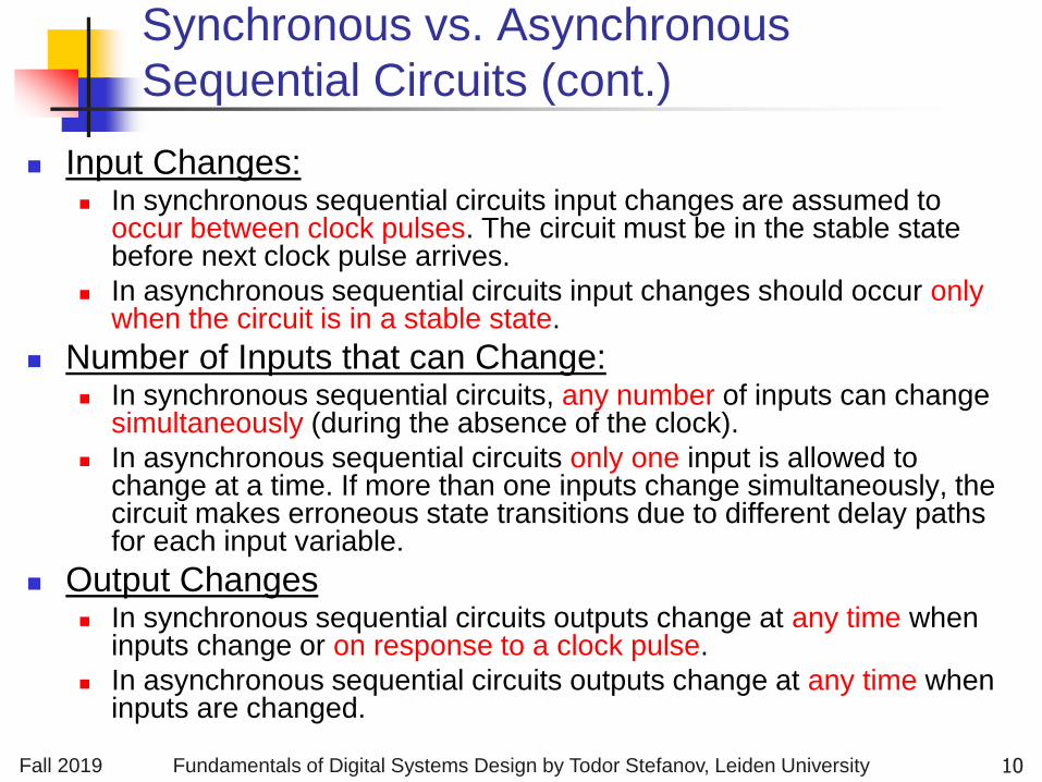
Synchronous vs. Asynchronous
Sequential Circuits (cont.)
Input Changes: In synchronous sequential circuits input changes are assumed to
occur between clock pulses. The circuit must be in the stable state before next clock pulse arrives.
In asynchronous sequential circuits input changes should occur only when the circuit is in a stable state.
Number of Inputs that can Change: In synchronous sequential circuits, any number of inputs can change
simultaneously (during the absence of the clock).
In asynchronous sequential circuits only one input is allowed to change at a time. If more than one inputs change simultaneously, the circuit makes erroneous state transitions due to different delay paths for each input variable.
Output Changes In synchronous sequential circuits outputs change at any time when
inputs change or on response to a clock pulse.
In asynchronous sequential circuits outputs change at any time when inputs are changed.
10

Fall 2019 Fundamentals of Digital Systems Design by Todor Stefanov, Leiden University
Synchronous vs. Asynchronous
Sequential Circuits (cont.)
Nowadays, most of the sequential circuits are synchronous due to their predictability and
relatively easy design and analysis.
An asynchronous circuit is preferred over synchronous circuit when high speed of operations are required asynchronous circuits respond immediately without having
to wait for a clock pulse.
Asynchronous sequential circuits cost less in terms of number of gates than the synchronous circuits therefore, for economical reasons, they find useful
applications.
11

Fall 2019 Fundamentals of Digital Systems Design by Todor Stefanov, Leiden University
Consider the sequential circuit below which has n inputs, m outputs, and p Flip-Flops (storage elements):
xj(t) – the present value of input xj ,i.e., the value prior to the application of a clock pulse at time t.
zj(t) – the present value of output zj ,i.e., the value prior to the application of a clock pulse at time t.
qj(t) – the present value stored by FFj ,i.e., the value prior to the application of a clock pulse at time t.
qj(t+1) – the next value to be stored by FFj ,i.e., the value stored after the application of a clock pulse at time t.
Synchronous Sequential Circuits:
Definitions and Notations
Combinational
Circuit
x1(t)
FF1
FFp
: :
: : xn(t)
z1(t)
zm(t)
qp(t+1)
q1(t+1)
qp(t)
q1(t)
t t+1 t-2 t-1
… …
t+2 clock
12

Fall 2019 Fundamentals of Digital Systems Design by Todor Stefanov, Leiden University
Synchronous Sequential Circuits:
Definitions and Notations (cont.)
Input Vector X(t) = ( x1(t),…,xn(t) ) – the values at the inputs prior to the application of a clock pulse at time t.
Output Vector Z(t) = ( z1(t),…,zm(t) ) – the values at the outputs prior to the application of a clock pulse at time t.
Present State Q(t) = ( q1(t),…,qp(t) ) – the values stored by the Flip-Flops prior to the application of a clock pulse at time t.
Next State Q(t+1) = ( q1(t+1),…,qp(t+1) ) – the values stored by the Flip-Flops after the application of a clock pulse at time t. In other words, the state one clock period later.
Z(t)
Q(t+1)
X(t)
Q(t)
Combinational
Circuit
x1(t)
FF1
FFp
: :
: : xn(t)
z1(t)
zm(t)
qp(t+1)
q1(t+1)
qp(t)
q1(t)
t t+1 t-2 t-1
… …
t+2 clock
13

Fall 2019 Fundamentals of Digital Systems Design by Todor Stefanov, Leiden University
Sequential Circuit Representations
Boolean Equations
Characteristic (Flip-Flop Input) Equations
Primary Output Equations
State Table
State Diagram
14
Fall 2019 Fundamentals of Digital Systems Design by Todor Stefanov, Leiden University
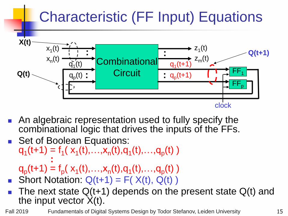
An algebraic representation used to fully specify the combinational logic that drives the inputs of the FFs.
Set of Boolean Equations: q1(t+1) = f1( x1(t),…,xn(t),q1(t),…,qp(t) ) : qp(t+1) = fp( x1(t),…,xn(t),q1(t),…,qp(t) )
Short Notation: Q(t+1) = F( X(t), Q(t) )
The next state Q(t+1) depends on the present state Q(t) and the input vector X(t).
Characteristic (FF Input) Equations
Q(t+1)
X(t)
Q(t)
Combinational
Circuit
x1(t)
FF1
FFp
: :
: : xn(t)
z1(t)
zm(t)
qp(t+1)
q1(t+1)
qp(t)
q1(t)
clock
15
Fall 2019 Fundamentals of Digital Systems Design by Todor Stefanov, Leiden University
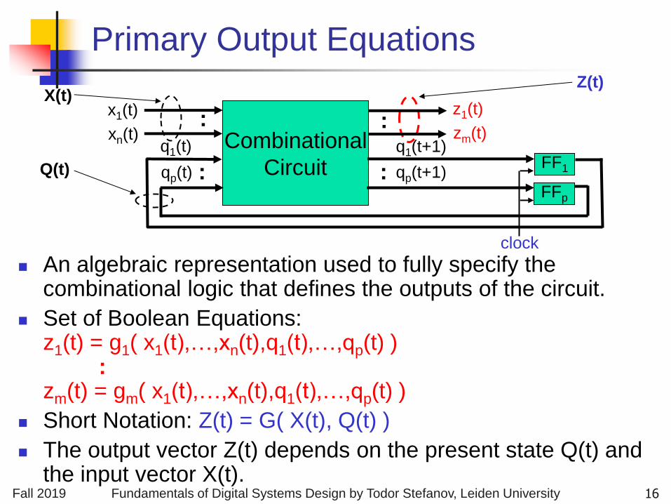
An algebraic representation used to fully specify the combinational logic that defines the outputs of the circuit.
Set of Boolean Equations: z1(t) = g1( x1(t),…,xn(t),q1(t),…,qp(t) ) : zm(t) = gm( x1(t),…,xn(t),q1(t),…,qp(t) )
Short Notation: Z(t) = G( X(t), Q(t) )
The output vector Z(t) depends on the present state Q(t) and the input vector X(t).
Primary Output Equations Z(t)
X(t)
Q(t)
Combinational
Circuit
x1(t)
FF1
FFp
: :
: : xn(t)
z1(t)
zm(t)
qp(t+1)
q1(t+1)
qp(t)
q1(t)
clock
16

Fall 2019 Fundamentals of Digital Systems Design by Todor Stefanov, Leiden University
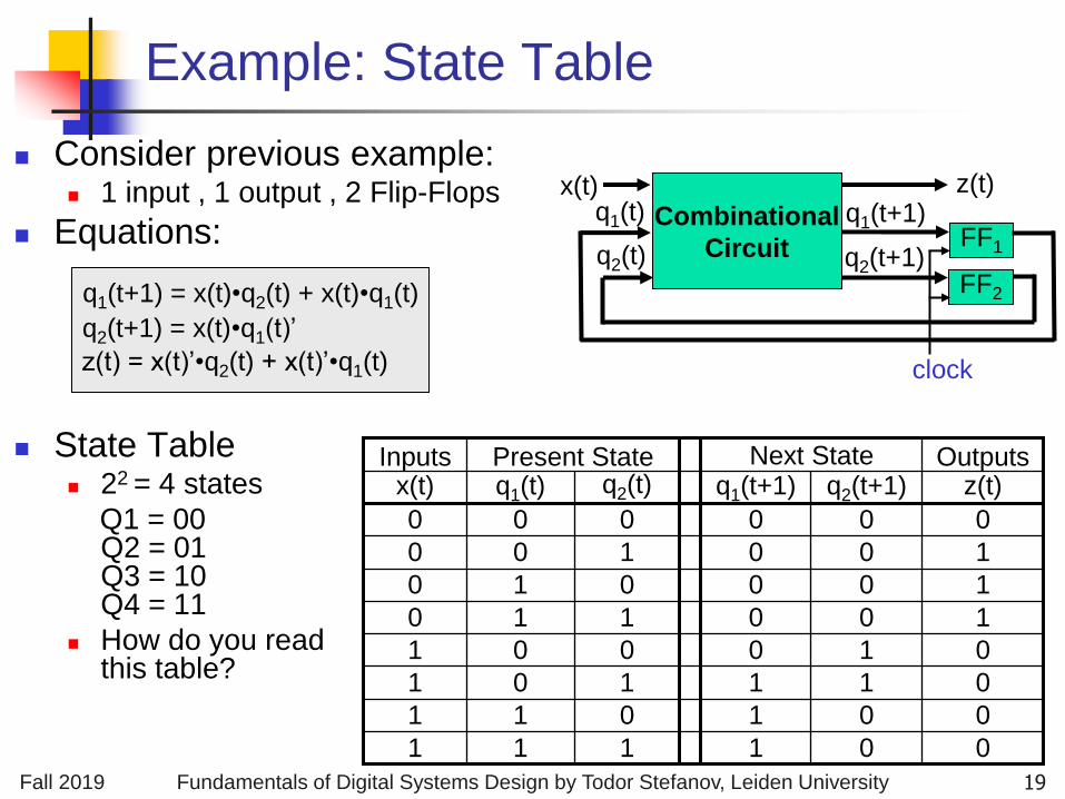
Example: Equations
Consider simple sequential circuit: 1 input , 1 output , 2 Flip-Flops
Characteristic (FF input) equations: q1(t+1) = f1( x(t), q1(t), q2(t) )
= q1(t)•x(t) + q2(t)•x(t) = ( q1(t) + q2(t) ) • x(t)
q2(t+1) = f2( x(t), q1(t), q2(t) ) = q1(t)’•x(t)
Primary output equations: z(t) = g( x(t), q1(t), q2(t) )
= q1(t)•x(t)’ + q2(t)•x(t)’ = ( q1(t) + q2(t) ) • x(t)’
q1(t+1)
q2(t+1) q2(t)
q1(t)
x(t) z(t)
FF2
FF1
Combinational Circuit
clock
Combinational
Circuit
x(t)
FF1
FF2
z(t)
q2(t+1)
q1(t+1)
q2(t)
q1(t)
clock
17

Fall 2019 Fundamentals of Digital Systems Design by Todor Stefanov, Leiden University
State Table
Enumerates the relationship between inputs, outputs, and states of the sequential circuit.
Given a circuit with n inputs, m outputs, and p Flip-Flops: The corresponding state table
contains 2n+p rows.
The corresponding state table contains n+2p+m columns.
xm(t) … qp(t+1) …
1 0
1 0
qp(t)
… …
… … ...
1 1
0 0
xn(t) … z1(t) q1(t+1) q1(t) x1(t)
1 1
… 0 0
Outputs Next State
… …
… …
Inputs
0 0
1 1
Present State
2n+p
n+p+p+m
Combinational
Circuit
x1(t)
FF1
FFp
zm(t)
qp(t+1)
q1(t+1)
qp(t)
q1(t)
clock
xn(t)
z1(t) : :
18
Fall 2019 Fundamentals of Digital Systems Design by Todor Stefanov, Leiden University
Example: State Table
Outputs Next State Present State Inputs
0
0
0
0
1
1
1
0
z(t)
0
0
1
1
0
0
0
0
q2(t+1)
1
1
1
0
0
0
0
0
q1(t+1)
1
1
1
1
0
0
0
0
x(t)
1 1
0 1
1 0
0 0
1 0
0 1
1
0
q1(t)
1
0
q2(t)
Combinational
Circuit
x(t)
FF1
FF2
z(t)
q2(t+1)
q1(t+1)
q2(t)
q1(t)
clock
q1(t+1) = x(t)•q2(t) + x(t)•q1(t)
q2(t+1) = x(t)•q1(t)’
z(t) = x(t)’•q2(t) + x(t)’•q1(t)
Consider previous example: 1 input , 1 output , 2 Flip-Flops
Equations:
State Table 22 = 4 states
Q1 = 00 Q2 = 01 Q3 = 10 Q4 = 11
How do you read this table?
19

Fall 2019 Fundamentals of Digital Systems Design by Todor Stefanov, Leiden University
State Table to/from Equations
State Table to Equations Treat the State Table as a Truth Table of Boolean functions to get the
Characteristic and Primary Output Equations.
You can derive the CSOP or CPOS form of the Equations directly using the right part of the State Table.
You can simplify the Equations using algebraic manipulations or K-maps.
State Table from Equations The Characteristic and Primary Output Equations are Boolean
functions.
Represent the Equations in a common Truth Table. This is actually the State Table.
xm(t) … qp(t+1) …
1 0
1 0
qp(t)
… …
… … ...
1 1
0 0
xn(t) … z1(t) q1(t+1) q1(t) x1(t)
1 1
… 0 0
Outputs Next State
… …
… …
Inputs
0 0
1 1
Present State
right part of the table
20

Fall 2019 Fundamentals of Digital Systems Design by Todor Stefanov, Leiden University
Example: State Table to Equations
Outputs Next State Present State Inputs
0
0
0
0
1
1
1
0
z(t)
0
0
1
1
0
0
0
0
q2(t+1)
1
1
1
0
0
0
0
0
q1(t+1)
1
1
1
1
0
0
0
0
x(t)
1 1
0 1
1 0
0 0
1 0
0 1
1
0
q1(t)
1
0
q2(t)
q1(t+1) = x(t)•q1(t)’•q2(t) +
x(t)•q1(t)•q2(t)’ +
x(t)•q1(t)•q2(t)
q2(t+1) = x(t)•q1(t)’•q2(t)’ +
x(t)•q1(t)’•q2(t)
z(t) = x(t)’•q1(t)’•q2(t) +
x(t)’•q1(t)•q2(t)’ +
x(t)’•q1(t)•q2(t)
q1q0
x
1
00
0
1 1 1
01 11 10
x
q2
q1 q1q0
x
1
00
0
1 1
01 11 10
x
q2
q1 q1q0
x
1
00
0
1
1 1
01 11 10
x
q2
q1
q1(t+1) = x(t)•q2(t) + x(t)•q1(t) q2(t+1) = x(t)•q1(t)’ z(t) = x(t)’•q2(t) + x(t)’•q1(t)
Simplified Equations
Equations in CSOP form
21

Fall 2019 Fundamentals of Digital Systems Design by Todor Stefanov, Leiden University
Example: State Table from Equations
q1(t+1) = x(t)•q2(t) + x(t)•q1(t)
q2(t+1) = x(t)•q1(t)’
z(t) = x(t)’•q2(t) + x(t)’•q1(t)
Identify the variables that are used on the right-hand side of the equations x(t), q1(t), and q2(t) 3 variables
List all possible combinations of the above variables: 23 = 8 combinations
For each combination evaluate the Equations: Find the value of q1(t+1), q2(t+1), and z(t)
Outputs Next State Present State Inputs
0
0
0
0
1
1
1
0
z(t)
0
0
1
1
0
0
0
0
q2(t+1)
1
1
1
0
0
0
0
0
q1(t+1)
1
1
1
1
0
0
0
0
x(t)
1 1
0 1
1 0
0 0
1 0
0 1
1
0
q1(t)
1
0
q2(t)
Follow the procedure
described below
22

Fall 2019 Fundamentals of Digital Systems Design by Todor Stefanov, Leiden University
State Diagram
Graph representation of a state table.
Graph node with label Q denotes state Q.
Graph edge with label X denotes transition
between two states when input X is applied.
The graph has 2p nodes and 2n+p edges. Why?
xm(t) … qp(t+1) …
1 0
1 0
qp(t)
… …
… … ...
1 1
0 0
xn(t) … z1(t) q1(t+1) q1(t) x1(t)
1 1
0 0
Outputs Next State
… …
… …
Inputs
0 0
1 1
Present State
Q1 Q2
X
23

Fall 2019 Fundamentals of Digital Systems Design by Todor Stefanov, Leiden University
Example: State Diagram
Outputs Next State Present State Inputs
0
0
0
0
1
1
1
0
z(t)
0
0
1
1
0
0
0
0
q2(t+1)
1
1
1
0
0
0
0
0
q1(t+1)
1
1
1
1
0
0
0
0
x(t)
1 1
0 1
1 0
0 0
1 0
0 1
1
0
q1(t)
1
0
q2(t)
00 01
1/0
10 111/0
0/1
1/00/10/1
1/0
0/0
• Possible states =
{ 00, 01, 10, 11 }
4 nodes in the diagram
• Possible Transitions =
#rows in table
8 edges in the diagram
Q1 Q2
X/Z
Reads as:
When at state Q1 and apply vector X,
we get output Z and proceed to state Q2.
24
Fall 2019 Fundamentals of Digital Systems Design by Todor Stefanov, Leiden University
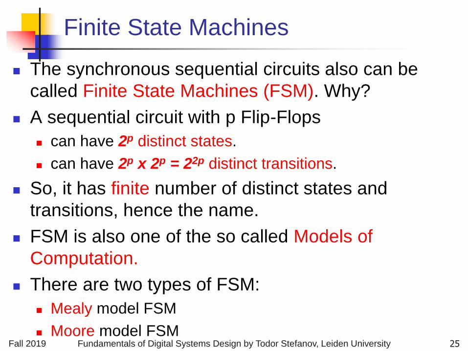
Finite State Machines
The synchronous sequential circuits also can be
called Finite State Machines (FSM). Why?
A sequential circuit with p Flip-Flops
can have 2p distinct states.
can have 2p x 2p = 22p distinct transitions.
So, it has finite number of distinct states and
transitions, hence the name.
FSM is also one of the so called Models of
Computation.
There are two types of FSM:
Mealy model FSM
Moore model FSM 25

Fall 2019 Fundamentals of Digital Systems Design by Todor Stefanov, Leiden University
Mealy Finite State Machine
Q(t+1) = C1( X(t), Q(t) )
Z(t) = C2( X(t), Q(t) )
Both outputs and next state depend directly on both primary
inputs AND present state.
Outputs are asynchronous, i.e., they can change in response
to any changes in the inputs, independent of the clock.
x1(t)
FF1
FFp
: :
: : xn(t)
z1(t)
zm(t)
qp(t+1)
q1(t+1)
qp(t)
q1(t)
t t+1 t-2 t-1
… …
t+2 clock
Combinational Logic
For Outputs
C2
Combinational Logic
For Next State
C1
26

Fall 2019 Fundamentals of Digital Systems Design by Todor Stefanov, Leiden University
Example: Mealy Machine
Consider simple sequential
circuit:
2 input , 2 output , 1 Flip-Flop
Characteristic (FF input)
equations:
q(t+1) = x1(t) + x2(t)•q(t)
Primary output equations:
z1(t) = x1(t)’ + x2(t)’•q(t)
z2(t) = x1(t)•q(t)
q(t+1) q(t)
x1(t) z1(t)
FF
Combinational Circuit
clock
Combinational
Circuit
x1(t)
FF
z1(t)
q(t+1) q(t)
clock
x2(t) z2(t)
x2(t)
z2(t)
27

Fall 2019 Fundamentals of Digital Systems Design by Todor Stefanov, Leiden University
Example: Mealy Machine (cont.)
Outputs NS PS Inputs
1
0
1
0
0
0
0
0
z2(t)
0
0
1
0
1
1
1
1
z1(t)
1
1
1
1
1
0
0
0
q(t+1)
1
1
1
1
0
0
0
0
x1(t)
1 1
0 1
1 0
0 0
1 0
0 1
1
0
x2(t)
1
0
q(t)
0 1
00/10 10/00
11/00
00/10
11/0101/10
01/10
10/11
• Possible states =
{ 0,1 }, thus 2 nodes in
state diagram
• Possible Transitions =
#rows in the table, thus 8
edges in state diagram
Q1 Q2
X/Z
Reads as:
When at state Q1 and apply vector X,
we get output Z and proceed to state Q2.
28
Fall 2019 Fundamentals of Digital Systems Design by Todor Stefanov, Leiden University
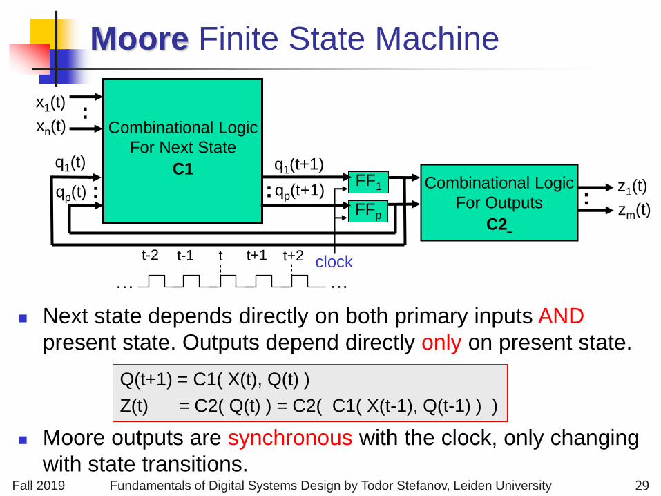
Moore Finite State Machine
Q(t+1) = C1( X(t), Q(t) )
Z(t) = C2( Q(t) ) = C2( C1( X(t-1), Q(t-1) ) )
Next state depends directly on both primary inputs AND
present state. Outputs depend directly only on present state.
Moore outputs are synchronous with the clock, only changing
with state transitions.
x1(t)
FF1
FFp
: :
:
:
xn(t)
z1(t)
zm(t) qp(t+1)
q1(t+1)
qp(t)
q1(t)
t t+1 t-2 t-1
… …
t+2 clock
Combinational Logic
For Outputs
C2
Combinational Logic
For Next State
C1
29

Fall 2019 Fundamentals of Digital Systems Design by Todor Stefanov, Leiden University
Example: Moore Machine
Consider simple sequential
circuit:
1 input , 1 output , 2 Flip-Flops
Characteristic (FF input)
equations:
q1(t+1) = x(t)•q1(t) + x(t)’•q2(t)
q2(t+1) = x(t)•q1(t)’
Primary output equations:
z(t) = q1(t) + q2(t)’
q1(t+1)
q2(t+1) q2(t)
q1(t)
x(t) z(t)
FF2
FF1
Combinational Circuit
clock
Combinational
Circuit
x(t)
FF2
FF1
q2(t+1)
q1(t+1)
q2(t)
q1(t)
clock
z(t)
30

Fall 2019 Fundamentals of Digital Systems Design by Todor Stefanov, Leiden University
Example: Moore Machine (cont.)
Outputs Next State Present State Inputs
1
1
0
1
1
1
0
1
z(t)
0
0
1
1
0
0
0
0
q2(t+1)
1
1
0
0
1
0
1
0
q1(t+1)
1
1
1
1
0
0
0
0
x(t)
1 1
0 1
1 0
0 0
1 0
0 1
1
0
q1(t)
1
0
q2(t)
00/1 01/0
1
10/1 11/1
0
0
1
0
1
0 1
• Possible states =
{ 00, 01, 10, 11 }
4 nodes in the diagram
• Possible Transitions =
#rows in table
8 edges in the diagram
Q1/Z1 Q2/Z2
X
Reads as:
When at state Q1 with output Z1 and apply input X,
we proceed to state Q2 with output Z2.
31
Fall 2019 Fundamentals of Digital Systems Design by Todor Stefanov, Leiden University
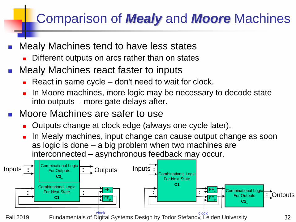
Comparison of Mealy and Moore Machines
Mealy Machines tend to have less states Different outputs on arcs rather than on states
Mealy Machines react faster to inputs React in same cycle – don't need to wait for clock.
In Moore machines, more logic may be necessary to decode state into outputs – more gate delays after.
Moore Machines are safer to use Outputs change at clock edge (always one cycle later).
In Mealy machines, input change can cause output change as soon as logic is done – a big problem when two machines are interconnected – asynchronous feedback may occur.
FF1
FFp
: :
:
:
clock
Combinational Logic
For Outputs
C2
Combinational Logic
For Next State
C1 FF1
FFp
: :
: :
clock
Combinational Logic
For Outputs
C2
Combinational Logic
For Next State
C1
Inputs Outputs Inputs
Outputs
32

Fall 2019 Fundamentals of Digital Systems Design by Todor Stefanov, Leiden University
Registered Mealy Machine (Really Moore)
x1(t)
FF1
FFp
: :
: : xn(t)
z1(t+1)
zm(t+1)
qp(t+1)
q1(t+1)
qp(t)
q1(t)
t t+1 t-2 t-1
… …
t+2 clock
Combinational Logic
For Outputs
C2
Combinational Logic
For Next State
C1
FF1
FFm
z1(t)
zm(t)
Synchronous (or registered) Mealy Machine
Registered outputs
Avoids “glitchy” outputs
Registered Mealy Machine is actually Moore Machine. Why?
View outputs as expanded state vector
So, we get Moore Machine with no output decoding
33


![Valtazar Bogisic: De La Forme Dite, Inokosna [1884]](https://img.pdfslide.us/doc/110x75/577d263f1a28ab4e1ea0a7aa/valtazar-bogisic-de-la-forme-dite-inokosna-1884.jpg)