Embed Size (px)
Citation preview
PhotoDetectors 3 – PD3Sergio Cova – SENSORS SIGNALS AND NOISE rv 2014/05/14
Sensors, Signals and Noise
COURSE OUTLINE
• Introduction
• Signals and Noise
• Filtering
• Sensors: PhotoDetectors 3 – PD3
1
PhotoDetectors 3 – PD3Sergio Cova – SENSORS SIGNALS AND NOISE rv 2014/05/14 2
Semiconductor Photo-Diodes (PD)
� PhotoDiode (PD) devices and carrier motion
� I-V characteristics and stationary equivalent circuit of PDs
� Photo-generation of free carriers and photon detection efficiency
� Dark-Current, detector noise and sensitive area
� Current signal in PDs
� PD equivalent circuit, dynamic response and sensitive area
� Carrier diffusion effects
� Evolution of the photodiode device structure
PhotoDetectors 3 – PD3Sergio Cova – SENSORS SIGNALS AND NOISE rv 2014/05/14 3
PhotoDiode (PD) devices
and carrier motion
PhotoDetectors 3 – PD3Sergio Cova – SENSORS SIGNALS AND NOISE rv 2014/05/14
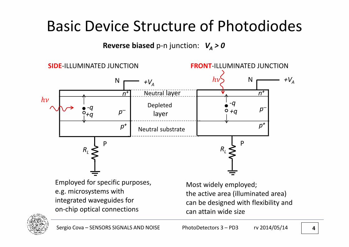
Basic Device Structure of Photodiodes
RL
p+
p--
n+
��-q+q
+VAN
P
Depleted
layer
RL
p+
p--
n+
��
-q
+q
N
P
+VA
Neutral layer
Neutral substrate
FRONT-ILLUMINATED JUNCTIONSIDE-ILLUMINATED JUNCTION
Employed for specific purposes,
e.g. microsystems with
integrated waveguides for
on-chip optical connections
Most widely employed;
the active area (illuminated area)
can be designed with flexibility and
can attain wide size
Reverse biased p-n junction: VA > 0
4
PhotoDetectors 3 – PD3Sergio Cova – SENSORS SIGNALS AND NOISE rv 2014/05/14
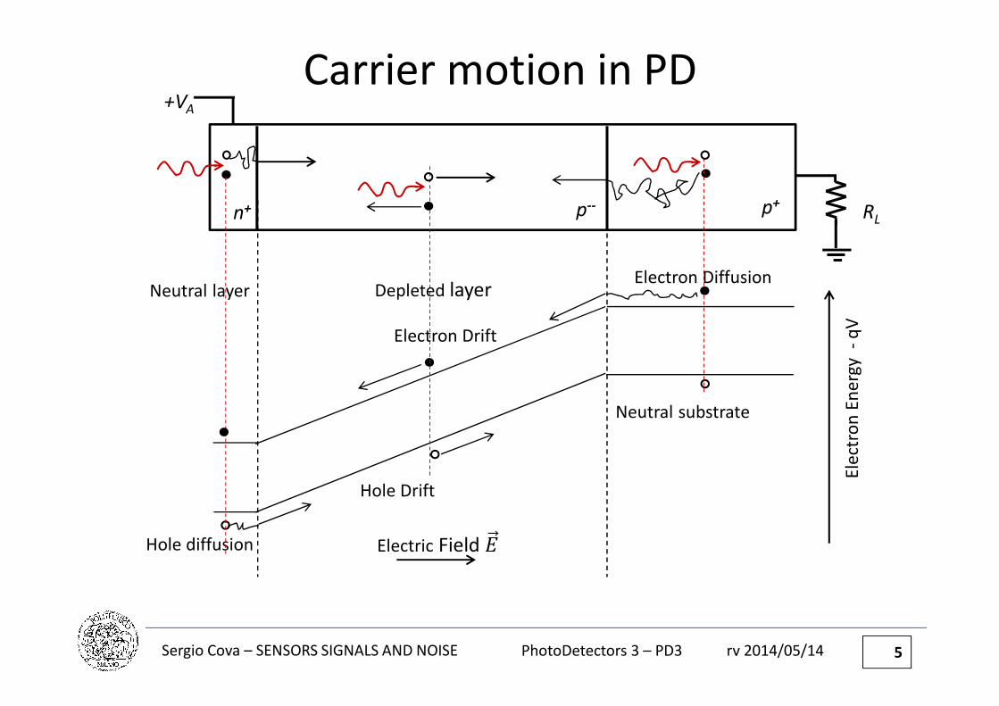
Carrier motion in PD
n+ p+p--
Electron Diffusion
Hole diffusion Electric Field �
Electron Drift
Ele
ctro
n E
ne
rgy
-q
V
Neutral layer Depleted layer
Neutral substrate
Hole Drift
RL
+VA
5
PhotoDetectors 3 – PD3Sergio Cova – SENSORS SIGNALS AND NOISE rv 2014/05/14
Carrier motion and Current in PDCarriers generated in the depleted layer:
• A carrier in the depleted layer induces opposite charges in the conductive electrodes
(neutral semiconductor layer and metal contact to the external circuit)
• The value of the induced charge on a given electrode depends on the carrier
distance from the electrode
• If the carrier moves the charge induced on the electrode varies, hence current flows
through the contact
Conclusion: a carrier drifting in the depleted layer causes current to flow through the
metal contact to the external circuit
Carriers generated in neutral regions:
• A carrier in a neutral region is surrounded by a huge population of other free carriers
• When the carrier moves the distribution of free carriers swifltly rearranges itself to
electrically screen any effect of the carrier motion on the external circuit
Conclusion: as long as it diffuses in a neutral region, a carrier does NOT cause current
to flow through the metal contact to the external circuit.
However, if by diffusion it reaches the edge of depletion layer before recombining,
then it drifts in the electric field and causes current to flow.
6
PhotoDetectors 3 – PD3Sergio Cova – SENSORS SIGNALS AND NOISE rv 2014/05/14 7
I-V characteristics of PhotoDiodes
PhotoDetectors 3 – PD3Sergio Cova – SENSORS SIGNALS AND NOISE rv 2014/05/14 8
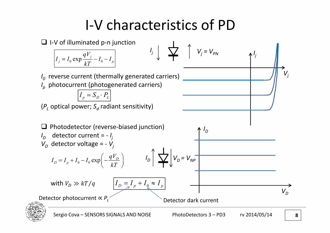
I-V characteristics of PD� I-V of illuminated p-n junction
I0 reverse current (thermally generated carriers)
Ip photocurrent (photogenerated carriers)
(PL optical power; Sd radiant sensitivity)
0 0expj
j p
qVI I I I
kT= − −
Ij
Vj
� Photodetector (reverse-biased junction)
ID detector current = - Ij
VD detector voltage = - Vj
with �� ≫ �� ⁄
Ij Vj = VPN
VD = VNPID
p D LI S P= ⋅
0 0 expD
D p
qVI I I I
kT
= + − −
0D p pI I I I= + ≈
Detector dark currentDetector photocurrent ∝ PL
VD
ID
PhotoDetectors 3 – PD3Sergio Cova – SENSORS SIGNALS AND NOISE rv 2014/05/14 9
Stationary operation of PD
stationary equivalent circuit:
photo-controlled current generator ID = SD∙PL
P
R
O D LV R I P= − ⋅ ∝
N
LINEAR PHOTOCURRENT MODE: PD with high reverse bias � ≫ �� ⁄
OPERATION WITH
PASSIVE LOAD
OPERATION WITH
ACTIVE LOAD
PL
+VA R
PL
+VA
O D LV R I P= ⋅ ∝
PhotoDetectors 3 – PD3Sergio Cova – SENSORS SIGNALS AND NOISE rv 2014/05/14 10
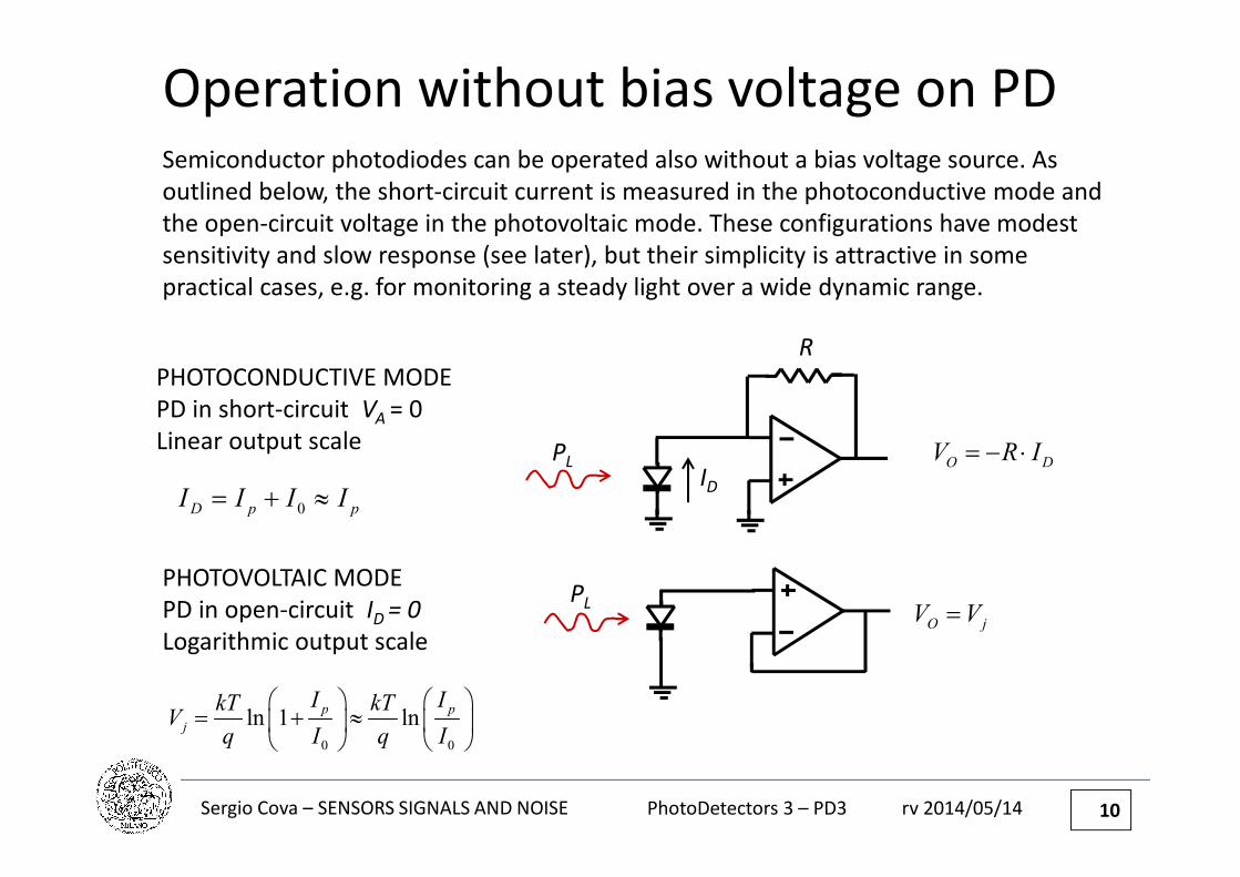
Operation without bias voltage on PD
PL
R
O DV R I= − ⋅
PHOTOCONDUCTIVE MODE
PD in short-circuit VA = 0
Linear output scale
PHOTOVOLTAIC MODE
PD in open-circuit ID = 0
Logarithmic output scale
PL
O jV V=
0 0
ln 1 lnp p
j
I IkT kTV
q I q I
= + ≈
ID
0D p pI I I I= + ≈
Semiconductor photodiodes can be operated also without a bias voltage source. As
outlined below, the short-circuit current is measured in the photoconductive mode and
the open-circuit voltage in the photovoltaic mode. These configurations have modest
sensitivity and slow response (see later), but their simplicity is attractive in some
practical cases, e.g. for monitoring a steady light over a wide dynamic range.
PhotoDetectors 3 – PD3Sergio Cova – SENSORS SIGNALS AND NOISE rv 2014/05/14 11
Photo-generation of free carriers
and photon detection efficiency
PhotoDetectors 3 – PD3Sergio Cova – SENSORS SIGNALS AND NOISE rv 2014/05/14
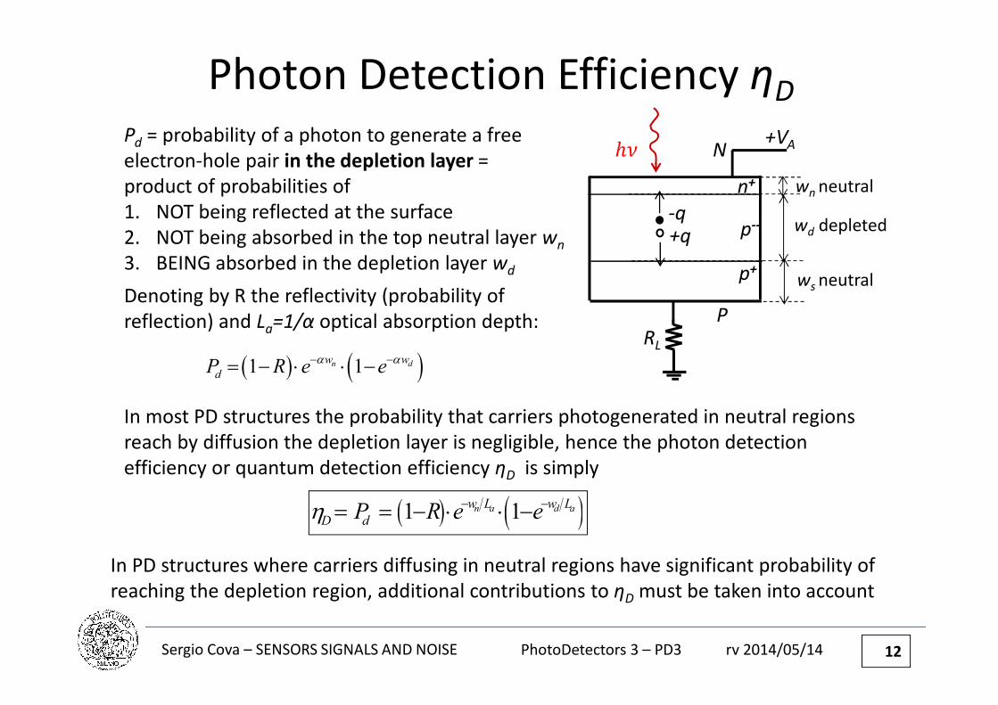
Photon Detection Efficiency ηD
12
RL
P
p+
p--
n+
��
-q+q
N+VA
wn neutral
wd depleted
ws neutral
Pd = probability of a photon to generate a free
electron-hole pair in the depletion layer =
product of probabilities of
1. NOT being reflected at the surface
2. NOT being absorbed in the top neutral layer wn
3. BEING absorbed in the depletion layer wd
Denoting by R the reflectivity (probability of
reflection) and La=1/α optical absorption depth:
( ) ( )1 1n dw w
dP R e eα α− −= − ⋅ ⋅ −
In most PD structures the probability that carriers photogenerated in neutral regions
reach by diffusion the depletion layer is negligible, hence the photon detection
efficiency or quantum detection efficiency ηD is simply
( ) ( )1 1n a d aw L w L
D dP R e eη − −= = − ⋅ ⋅ −
In PD structures where carriers diffusing in neutral regions have significant probability of
reaching the depletion region, additional contributions to ηD must be taken into account
PhotoDetectors 3 – PD3Sergio Cova – SENSORS SIGNALS AND NOISE rv 2014/05/14 13
Photon Detection Efficiency ηD
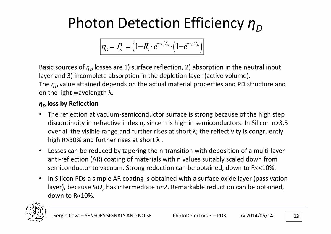
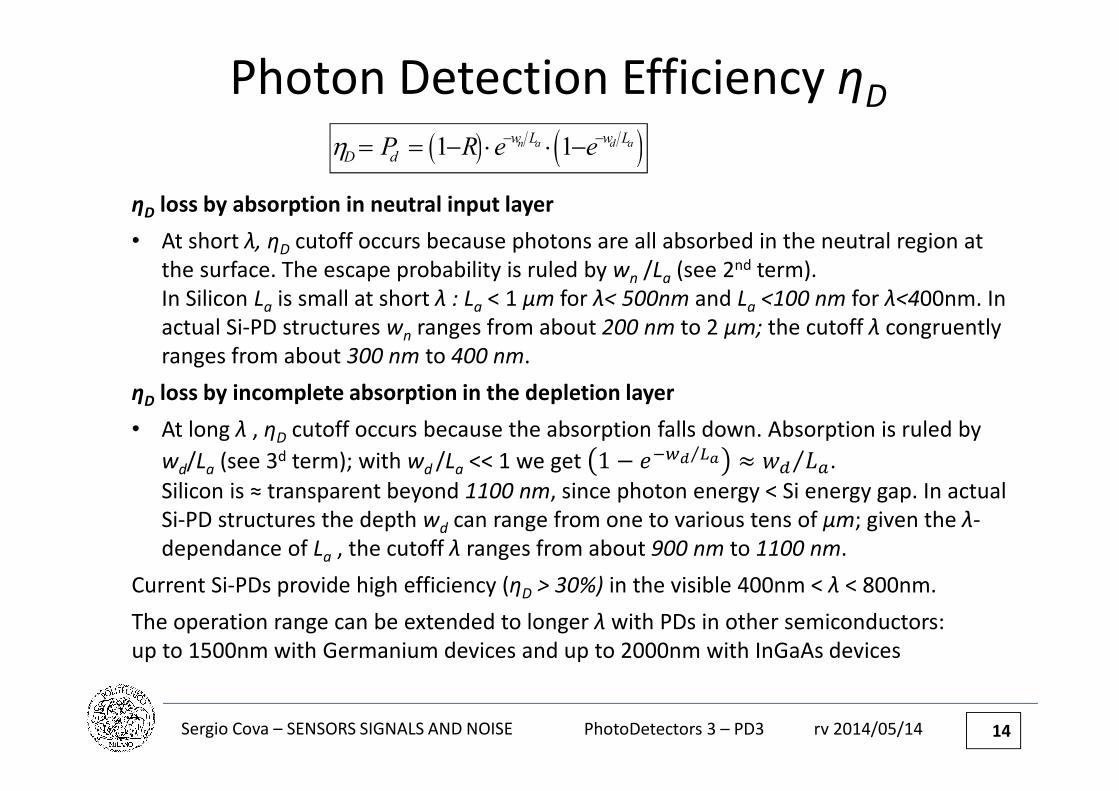
( ) ( )1 1n a d aw L w L
D dP R e eη − −= = − ⋅ ⋅ −
Basic sources of ηD losses are 1) surface reflection, 2) absorption in the neutral input
layer and 3) incomplete absorption in the depletion layer (active volume).
The ηD value attained depends on the actual material properties and PD structure and
on the light wavelength λ.
ηD loss by Reflection
• The reflection at vacuum-semiconductor surface is strong because of the high step
discontinuity in refractive index n, since n is high in semiconductors. In Silicon n>3,5
over all the visible range and further rises at short λ; the reflectivity is congruently
high R>30% and further rises at short λ .
• Losses can be reduced by tapering the n-transition with deposition of a multi-layer
anti-reflection (AR) coating of materials with n values suitably scaled down from
semiconductor to vacuum. Strong reduction can be obtained, down to R<<10%.
• In Silicon PDs a simple AR coating is obtained with a surface oxide layer (passivation
layer), because SiO2 has intermediate n≈2. Remarkable reduction can be obtained,
down to R≈10%.
PhotoDetectors 3 – PD3Sergio Cova – SENSORS SIGNALS AND NOISE rv 2014/05/14 14
Photon Detection Efficiency ηD
ηD loss by absorption in neutral input layer
• At short λ, ηD cutoff occurs because photons are all absorbed in the neutral region at
the surface. The escape probability is ruled by wn /La (see 2nd term).
In Silicon La is small at short λ : La < 1 μm for λ< 500nm and La <100 nm for λ<400nm. In
actual Si-PD structures wn ranges from about 200 nm to 2 μm; the cutoff λ congruently
ranges from about 300 nm to 400 nm.
ηD loss by incomplete absorption in the depletion layer
• At long λ , ηD cutoff occurs because the absorption falls down. Absorption is ruled by
wd/La (see 3d term); with wd /La << 1 we get 1 − ���� ��⁄ ≈ �� ��⁄ .
Silicon is ≈ transparent beyond 1100 nm, since photon energy < Si energy gap. In actual
Si-PD structures the depth wd can range from one to various tens of μm; given the λ-
dependance of La , the cutoff λ ranges from about 900 nm to 1100 nm.
Current Si-PDs provide high efficiency (ηD > 30%) in the visible 400nm < λ < 800nm.
The operation range can be extended to longer λ with PDs in other semiconductors:
up to 1500nm with Germanium devices and up to 2000nm with InGaAs devices
( ) ( )1 1n a d aw L w L
D dP R e eη − −= = − ⋅ ⋅ −
PhotoDetectors 3 – PD3Sergio Cova – SENSORS SIGNALS AND NOISE rv 2014/05/14 15
Dark-Current, detector noise
and sensitive area
PhotoDetectors 3 – PD3Sergio Cova – SENSORS SIGNALS AND NOISE rv 2014/05/14 16
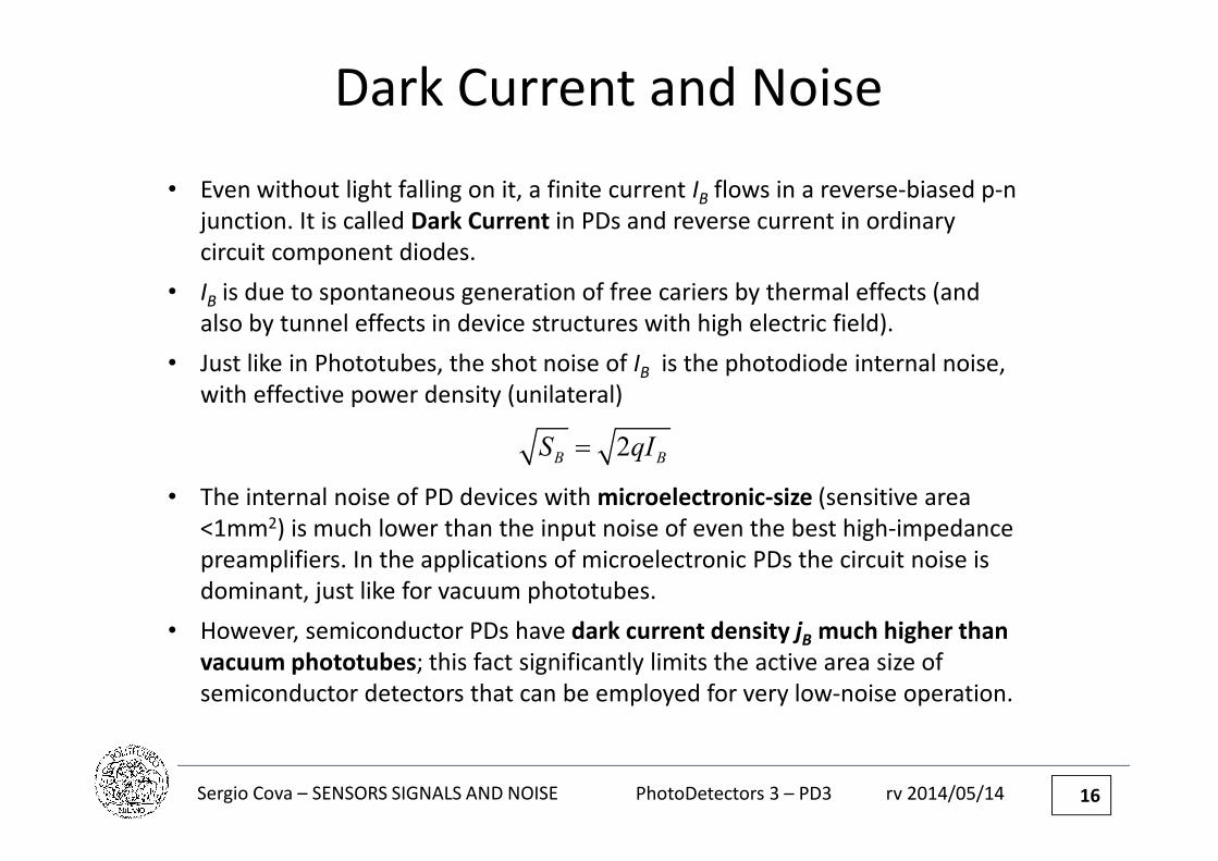
Dark Current and Noise
• Even without light falling on it, a finite current IB flows in a reverse-biased p-n
junction. It is called Dark Current in PDs and reverse current in ordinary
circuit component diodes.
• IB is due to spontaneous generation of free cariers by thermal effects (and
also by tunnel effects in device structures with high electric field).
• Just like in Phototubes, the shot noise of IB is the photodiode internal noise,
with effective power density (unilateral)
• The internal noise of PD devices with microelectronic-size (sensitive area
<1mm2) is much lower than the input noise of even the best high-impedance
preamplifiers. In the applications of microelectronic PDs the circuit noise is
dominant, just like for vacuum phototubes.
• However, semiconductor PDs have dark current density jB much higher than
vacuum phototubes; this fact significantly limits the active area size of
semiconductor detectors that can be employed for very low-noise operation.
2B BS qI=
PhotoDetectors 3 – PD3Sergio Cova – SENSORS SIGNALS AND NOISE rv 2014/05/14
Trap Assisted
Tunneling
17
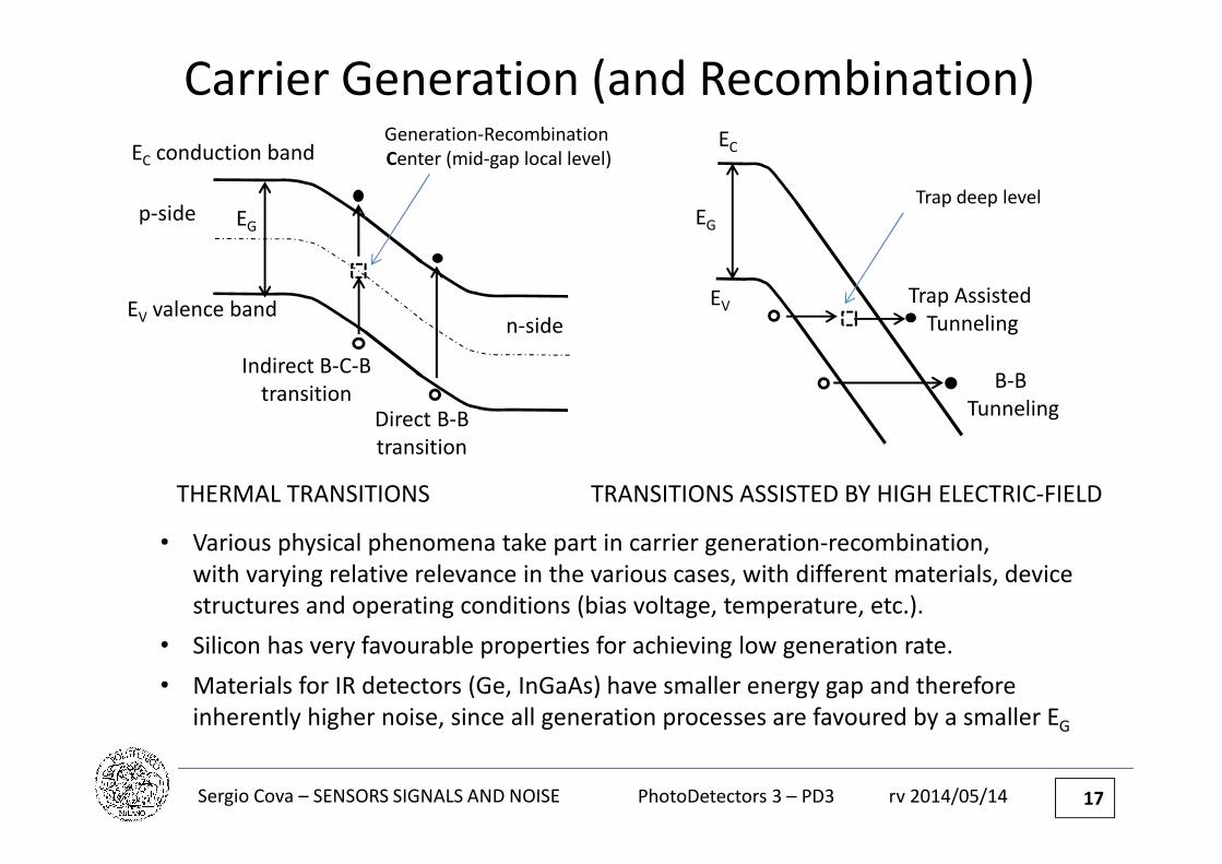
Carrier Generation (and Recombination)
EG
EC conduction band
EV valence band
Direct B-B
transition
Indirect B-C-B
transition
Generation-Recombination
Center (mid-gap local level)
B-B
Tunneling
Trap deep levelEG
EC
p-side
n-side
THERMAL TRANSITIONS TRANSITIONS ASSISTED BY HIGH ELECTRIC-FIELD
EV
• Various physical phenomena take part in carrier generation-recombination,
with varying relative relevance in the various cases, with different materials, device
structures and operating conditions (bias voltage, temperature, etc.).
• Silicon has very favourable properties for achieving low generation rate.
• Materials for IR detectors (Ge, InGaAs) have smaller energy gap and therefore
inherently higher noise, since all generation processes are favoured by a smaller EG
PhotoDetectors 3 – PD3Sergio Cova – SENSORS SIGNALS AND NOISE rv 2014/05/14
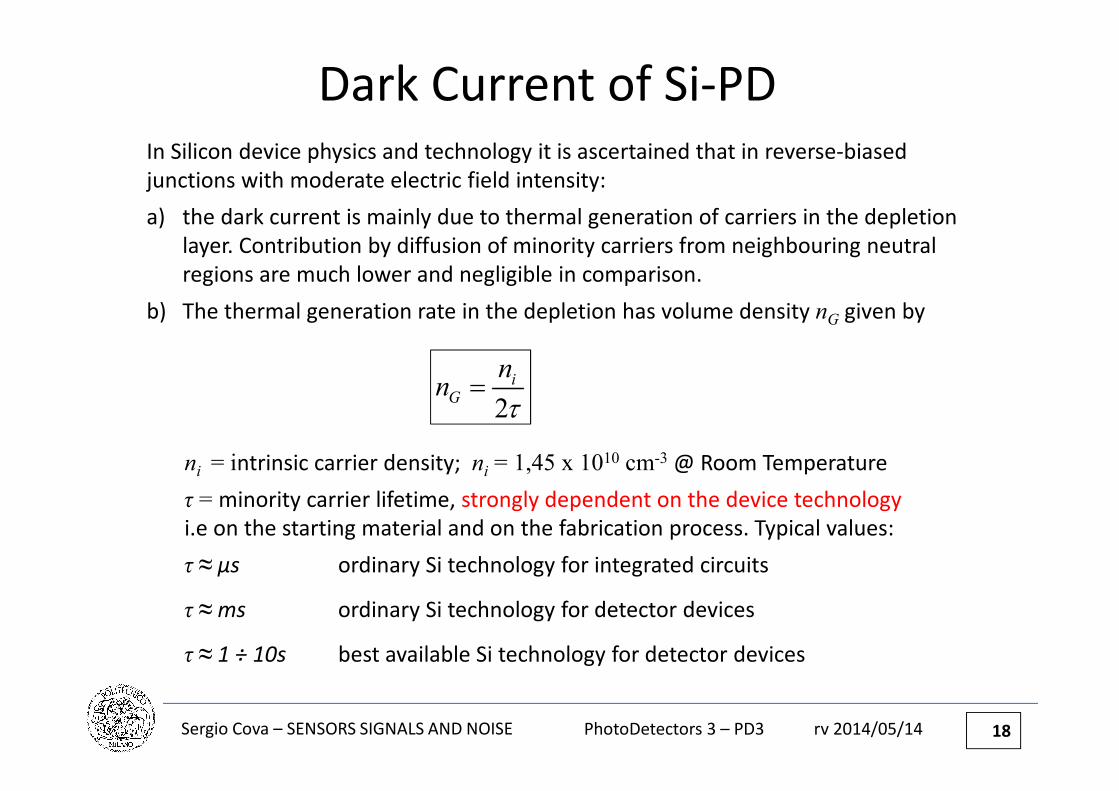
Dark Current of Si-PDIn Silicon device physics and technology it is ascertained that in reverse-biased
junctions with moderate electric field intensity:
a) the dark current is mainly due to thermal generation of carriers in the depletion
layer. Contribution by diffusion of minority carriers from neighbouring neutral
regions are much lower and negligible in comparison.
b) The thermal generation rate in the depletion has volume density nG given by
ni = intrinsic carrier density; ni = 1,45 x 1010 cm-3 @ Room Temperature
τ = minority carrier lifetime, strongly dependent on the device technology
i.e on the starting material and on the fabrication process. Typical values:
τ ≈ µs ordinary Si technology for integrated circuits
τ ≈ms ordinary Si technology for detector devices
τ ≈ 1 ÷ 10s best available Si technology for detector devices
2
iG
nn
τ=
18
PhotoDetectors 3 – PD3Sergio Cova – SENSORS SIGNALS AND NOISE rv 2014/05/14
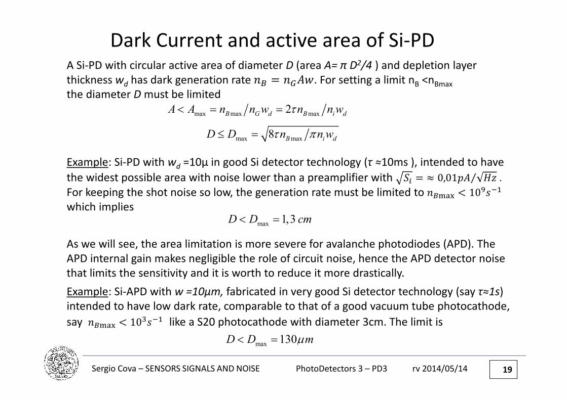
Dark Current and active area of Si-PDA Si-PD with circular active area of diameter D (area A= π D2/4 ) and depletion layer
thickness wd has dark generation rate �� = ����. For setting a limit nB <nBmax
the diameter D must be limited
Example: Si-PD with wd =10μ in good Si detector technology (τ ≈10ms ), intended to have
the widest possible area with noise lower than a preamplifier with � = ≈ 0,01#� $%⁄ .
For keeping the shot noise so low, the generation rate must be limited to ��&'( < 10*+�,
which implies
As we will see, the area limitation is more severe for avalanche photodiodes (APD). The
APD internal gain makes negligible the role of circuit noise, hence the APD detector noise
that limits the sensitivity and it is worth to reduce it more drastically.
Example: Si-APD with w =10μm, fabricated in very good Si detector technology (say τ≈1s)
intended to have low dark rate, comparable to that of a good vacuum tube photocathode,
say ��&'( < 10-+�, like a S20 photocathode with diameter 3cm. The limit is
max max8 B i dD D n n wτ π≤ =
19
max max max2B G d B i dA A n n w n n wτ< = =
max 1,3D D cm< =
max 130D D mµ< =
PhotoDetectors 3 – PD3Sergio Cova – SENSORS SIGNALS AND NOISE rv 2014/05/14 20
Current signal in PDs
PhotoDetectors 3 – PD3Sergio Cova – SENSORS SIGNALS AND NOISE rv 2014/05/14 21
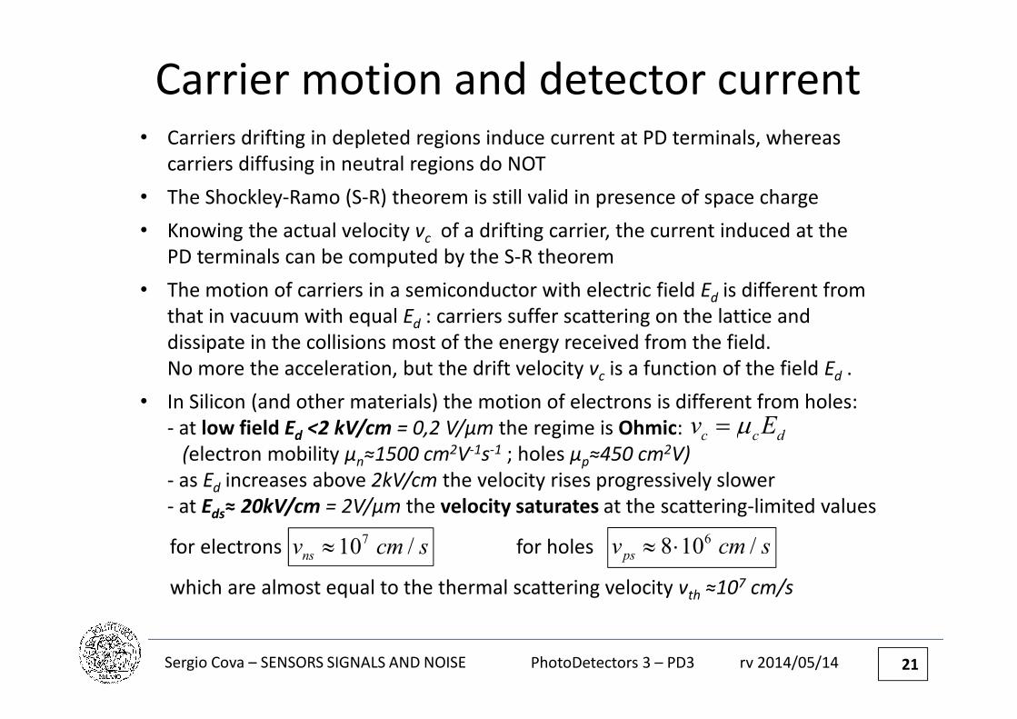
Carrier motion and detector current• Carriers drifting in depleted regions induce current at PD terminals, whereas
carriers diffusing in neutral regions do NOT
• The Shockley-Ramo (S-R) theorem is still valid in presence of space charge
• Knowing the actual velocity vc of a drifting carrier, the current induced at the
PD terminals can be computed by the S-R theorem
• The motion of carriers in a semiconductor with electric field Ed is different from
that in vacuum with equal Ed : carriers suffer scattering on the lattice and
dissipate in the collisions most of the energy received from the field.
No more the acceleration, but the drift velocity vc is a function of the field Ed .
• In Silicon (and other materials) the motion of electrons is different from holes:
- at low field Ed <2 kV/cm = 0,2 V/μm the regime is Ohmic:
(electron mobility μn≈1500 cm2V-1s-1 ; holes μp≈450 cm2V)
- as Ed increases above 2kV/cm the velocity rises progressively slower
- at Eds≈ 20kV/cm = 2V/μm the velocity saturates at the scattering-limited values
for electrons for holes
which are almost equal to the thermal scattering velocity vth ≈107 cm/s
c c dv Eµ=
710 /nsv cm s≈ 68 10 /psv cm s≈ ⋅
PhotoDetectors 3 – PD3Sergio Cova – SENSORS SIGNALS AND NOISE rv 2014/05/14
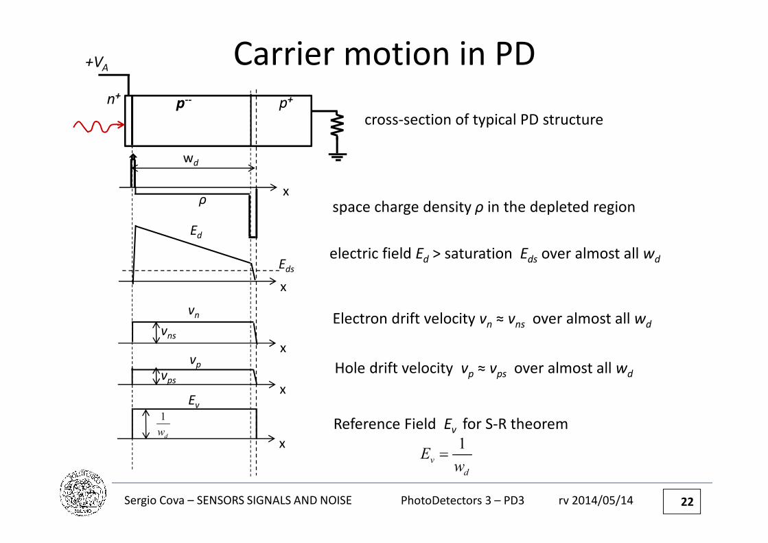
Carrier motion in PD
22
n+p+p--
+VA
cross-section of typical PD structure
electric field Ed > saturation Eds over almost all wd
x
x
x
Eds
Electron drift velocity vn ≈ vns over almost all wd
Hole drift velocity vp ≈ vps over almost all wd
x
Reference Field Ev for S-R theorem
vps
vns
Ev
vn
vp
1v
d
Ew
=
1
dw
wd
Ed
space charge density ρ in the depleted regionx
ρ
PhotoDetectors 3 – PD3Sergio Cova – SENSORS SIGNALS AND NOISE rv 2014/05/14
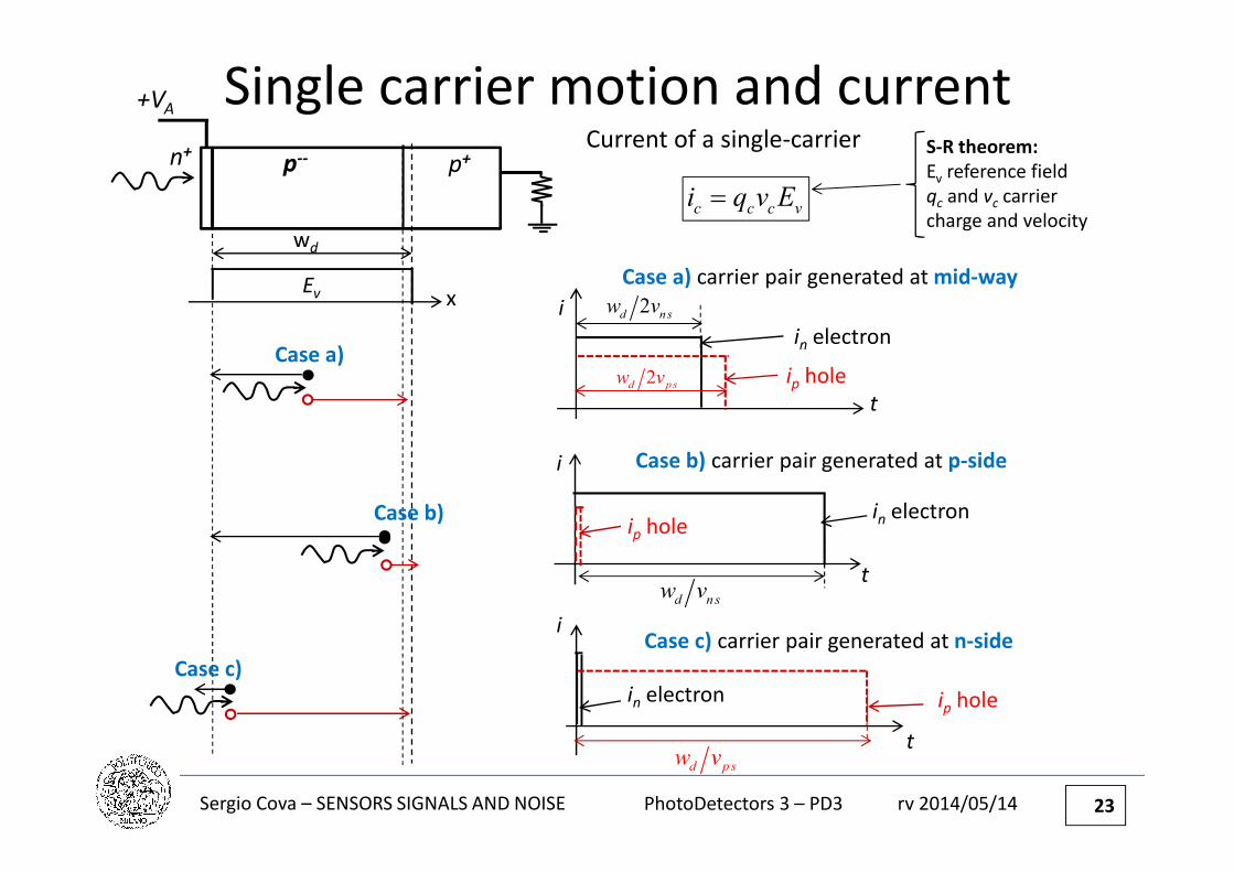
Single carrier motion and currentn+
p+p--
+VA
23
Current of a single-carrier
xEv
wd
Case a) carrier pair generated at mid-way
Case b) carrier pair generated at p-side
Case c) carrier pair generated at n-side
i
2d p sw v
2d n s
w v
in electron
ip hole
t
i
d n sw v
ip holein electron
t
i
in electron
d p sw v
ip hole
t
Case a)
Case b)
Case c)
c c c vi q v E=
S-R theorem:
Ev reference field
qc and vc carrier
charge and velocity
PhotoDetectors 3 – PD3Sergio Cova – SENSORS SIGNALS AND NOISE rv 2014/05/14 24
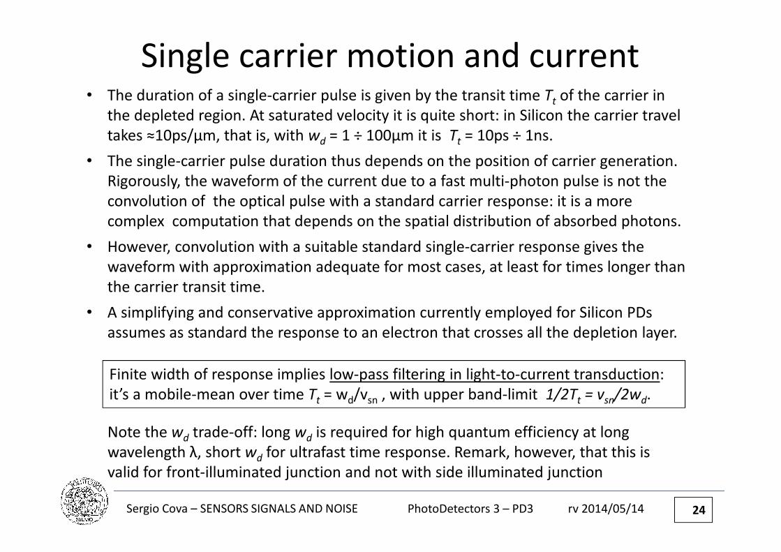
Single carrier motion and current• The duration of a single-carrier pulse is given by the transit time Tt of the carrier in
the depleted region. At saturated velocity it is quite short: in Silicon the carrier travel
takes ≈10ps/μm, that is, with wd = 1 ÷ 100μm it is Tt = 10ps ÷ 1ns.
• The single-carrier pulse duration thus depends on the position of carrier generation.
Rigorously, the waveform of the current due to a fast multi-photon pulse is not the
convolution of the optical pulse with a standard carrier response: it is a more
complex computation that depends on the spatial distribution of absorbed photons.
• However, convolution with a suitable standard single-carrier response gives the
waveform with approximation adequate for most cases, at least for times longer than
the carrier transit time.
• A simplifying and conservative approximation currently employed for Silicon PDs
assumes as standard the response to an electron that crosses all the depletion layer.
Finite width of response implies low-pass filtering in light-to-current transduction:
it’s a mobile-mean over time Tt = wd/vsn , with upper band-limit 1/2Tt = vsn/2wd.
Note the wd trade-off: long wd is required for high quantum efficiency at long
wavelength λ, short wd for ultrafast time response. Remark, however, that this is
valid for front-illuminated junction and not with side illuminated junction
PhotoDetectors 3 – PD3Sergio Cova – SENSORS SIGNALS AND NOISE rv 2014/05/14 25
PD equivalent circuit,
dynamic response and sensitive area
PhotoDetectors 3 – PD3Sergio Cova – SENSORS SIGNALS AND NOISE rv 2014/05/14 26
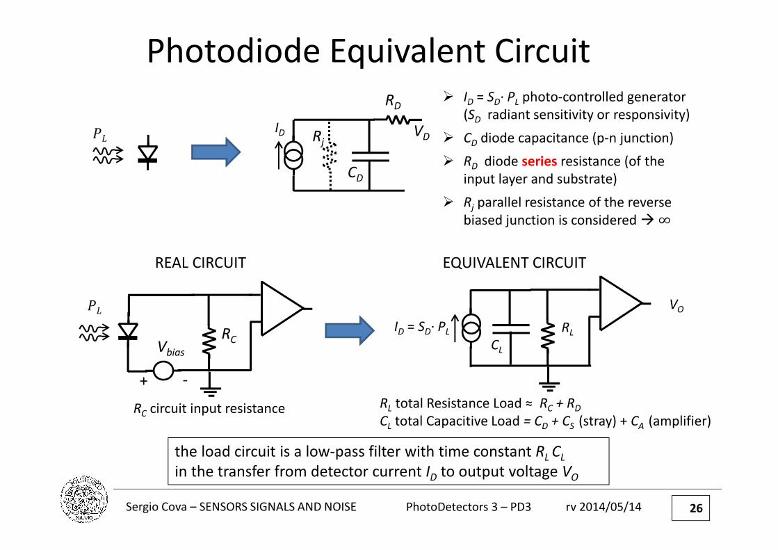
Photodiode Equivalent Circuit
CD
RD
.�ID
� ID = SD∙ PL photo-controlled generator
(SD radiant sensitivity or responsivity)
� CD diode capacitance (p-n junction)
� RD diode series resistance (of the
input layer and substrate)
� Rj parallel resistance of the reverse
biased junction is considered � ∞
RCVbias
.�
REAL CIRCUIT
-+
RL total Resistance Load ≈ RC + RD
CL total Capacitive Load = CD + CS (stray) + CA (amplifier)
the load circuit is a low-pass filter with time constant RL CL
in the transfer from detector current ID to output voltage VO
RjVD
RL
CL
VO
ID = SD∙ PL
EQUIVALENT CIRCUIT
RC circuit input resistance
PhotoDetectors 3 – PD3Sergio Cova – SENSORS SIGNALS AND NOISE rv 2014/05/14 27
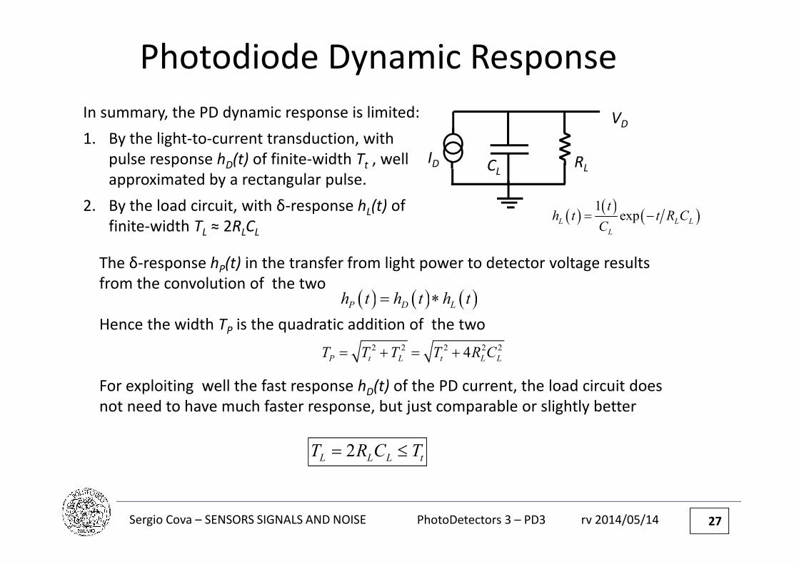
Photodiode Dynamic Response
VD
CLRL
ID
In summary, the PD dynamic response is limited:
1. By the light-to-current transduction, with
pulse response hD(t) of finite-width Tt , well
approximated by a rectangular pulse.
2. By the load circuit, with δ-response hL(t) of
finite-width TL ≈ 2RLCL
( ) ( ) ( )1
expL L L
L
th t t R C
C= −
The δ-response hP(t) in the transfer from light power to detector voltage results
from the convolution of the two
Hence the width TP is the quadratic addition of the two
For exploiting well the fast response hD(t) of the PD current, the load circuit does
not need to have much faster response, but just comparable or slightly better
( ) ( ) ( )P D Lh t h t h t= ∗
2 2 2 2 24P t L t L L
T T T T R C= + = +
2L L L tT R C T= ≤
PhotoDetectors 3 – PD3Sergio Cova – SENSORS SIGNALS AND NOISE rv 2014/05/14 28
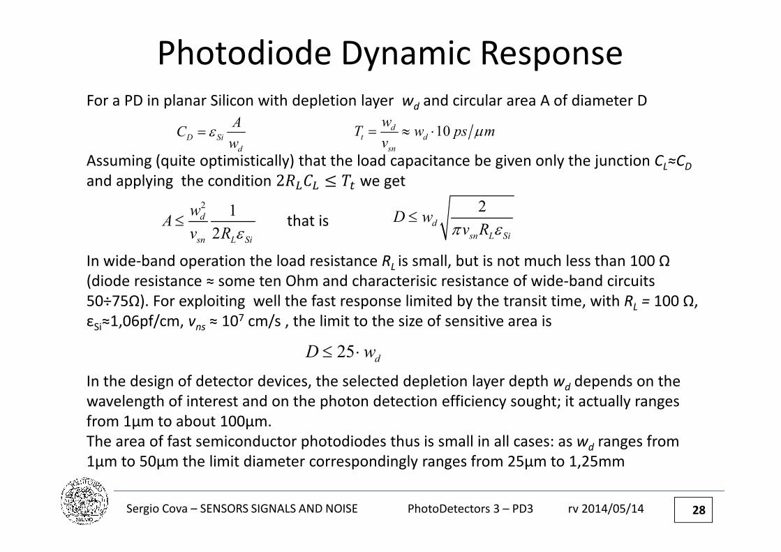
Photodiode Dynamic ResponseFor a PD in planar Silicon with depletion layer wd and circular area A of diameter D
Assuming (quite optimistically) that the load capacitance be given only the junction CL≈CD
and applying the condition 21�2� ≤ �4 we get
that is
In wide-band operation the load resistance RL is small, but is not much less than 100 Ω
(diode resistance ≈ some ten Ohm and characterisic resistance of wide-band circuits
50÷75Ω). For exploiting well the fast response limited by the transit time, with RL = 100 Ω,
εSi≈1,06pf/cm, vns ≈ 107 cm/s , the limit to the size of sensitive area is
In the design of detector devices, the selected depletion layer depth wd depends on the
wavelength of interest and on the photon detection efficiency sought; it actually ranges
from 1μm to about 100μm.
The area of fast semiconductor photodiodes thus is small in all cases: as wd ranges from
1μm to 50μm the limit diameter correspondingly ranges from 25μm to 1,25mm
10dt d
sn
wT w ps m
vµ= ≈ ⋅
D Si
d
AC
wε=
21
2
d
sn L Si
wA
v R ε≤
2d
sn L Si
D wv Rπ ε
≤
25 dD w≤ ⋅
PhotoDetectors 3 – PD3Sergio Cova – SENSORS SIGNALS AND NOISE rv 2014/05/14 29
Carrier diffusion effects
PhotoDetectors 3 – PD3Sergio Cova – SENSORS SIGNALS AND NOISE rv 2014/05/14
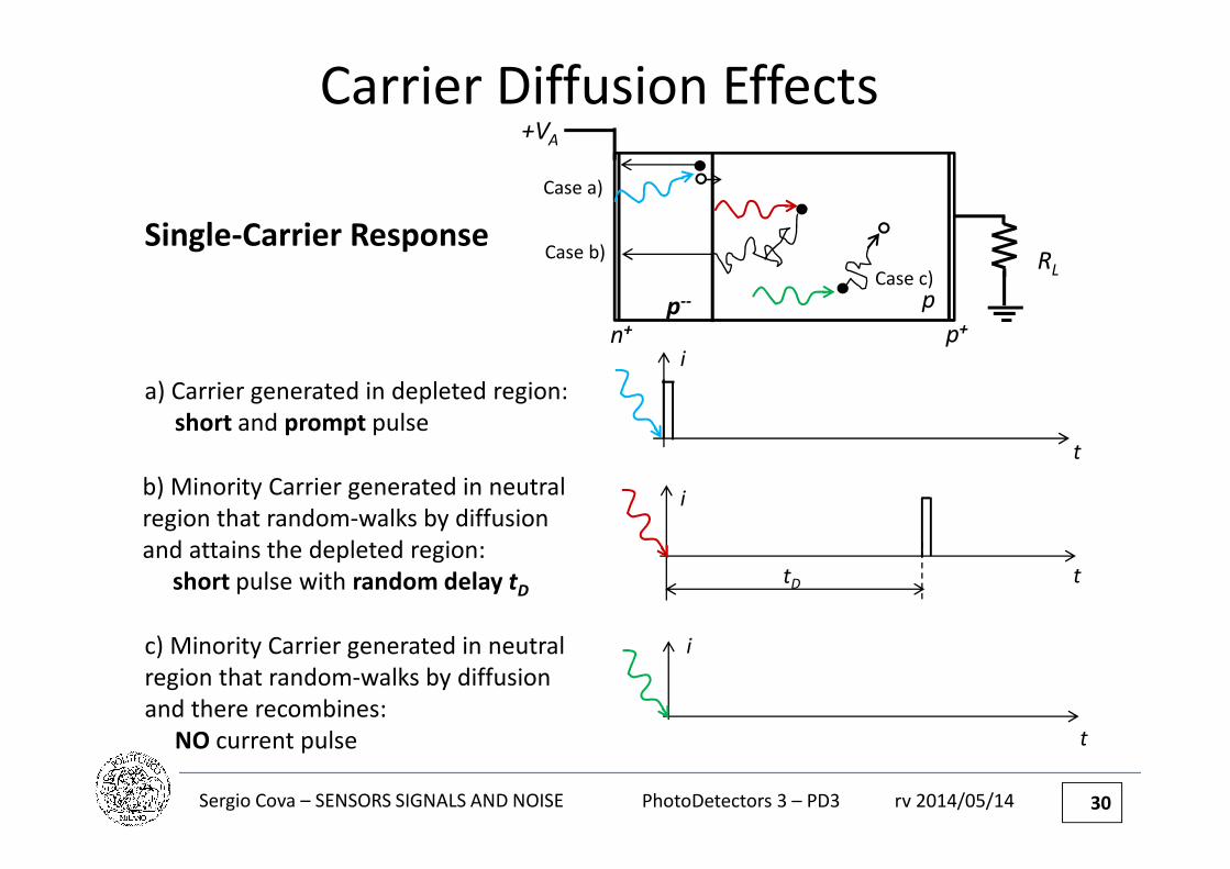
Carrier Diffusion Effects
n+ p+
p--
RL
+VA
30
p
Case a)
Case b)
Case c)
Single-Carrier Response
a) Carrier generated in depleted region:
short and prompt pulse
b) Minority Carrier generated in neutral
region that random-walks by diffusion
and attains the depleted region:
short pulse with random delay tD
c) Minority Carrier generated in neutral
region that random-walks by diffusion
and there recombines:
NO current pulse
i
t
tD
i
t
i
t
PhotoDetectors 3 – PD3Sergio Cova – SENSORS SIGNALS AND NOISE rv 2014/05/14
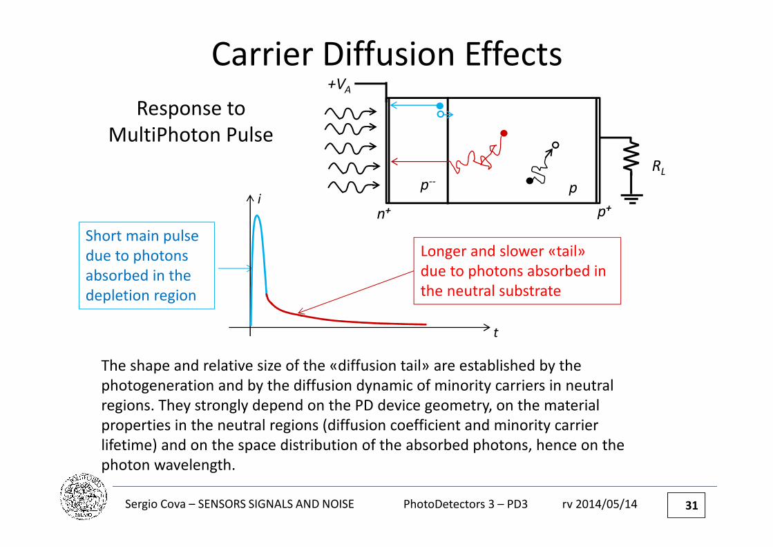
Carrier Diffusion Effects
p+
p--
RL
+VA
31
p
Response to
MultiPhoton Pulse
Short main pulse
due to photons
absorbed in the
depletion region
n+
Longer and slower «tail»
due to photons absorbed in
the neutral substrate
t
i
The shape and relative size of the «diffusion tail» are established by the
photogeneration and by the diffusion dynamic of minority carriers in neutral
regions. They strongly depend on the PD device geometry, on the material
properties in the neutral regions (diffusion coefficient and minority carrier
lifetime) and on the space distribution of the absorbed photons, hence on the
photon wavelength.
PhotoDetectors 3 – PD3Sergio Cova – SENSORS SIGNALS AND NOISE rv 2014/05/14
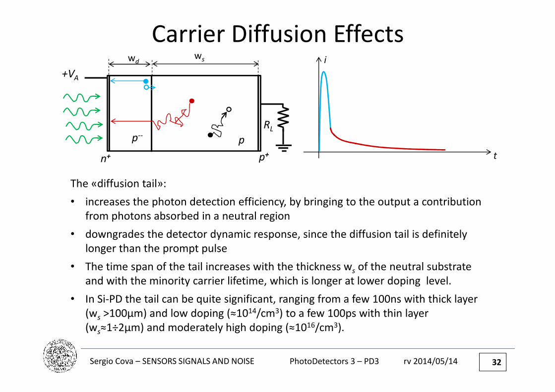
Carrier Diffusion Effects
n+ p+
p--
RL
+VA
32
p
t
i
The «diffusion tail»:
• increases the photon detection efficiency, by bringing to the output a contribution
from photons absorbed in a neutral region
• downgrades the detector dynamic response, since the diffusion tail is definitely
longer than the prompt pulse
• The time span of the tail increases with the thickness ws of the neutral substrate
and with the minority carrier lifetime, which is longer at lower doping level.
• In Si-PD the tail can be quite significant, ranging from a few 100ns with thick layer
(ws >100μm) and low doping (≈1014/cm3) to a few 100ps with thin layer
(ws≈1÷2μm) and moderately high doping (≈1016/cm3).
wdws
PhotoDetectors 3 – PD3Sergio Cova – SENSORS SIGNALS AND NOISE rv 2014/05/14 33
Evolution of the photodiode device structure
PhotoDetectors 3 – PD3Sergio Cova – SENSORS SIGNALS AND NOISE rv 2014/05/14 34
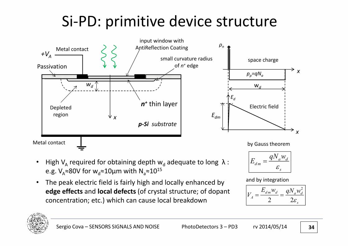
Si-PD: primitive device structure
x
x
Edm
Electric field
space charge
wd
Metal contact
Metal contact
Passivation
input window with
AntiReflection Coating
p-Si substrate
n+ thin layer
wd
Depleted
region
small curvature radius
of n+ edge
x
by Gauss theorem
Ed
ρn
pp=qNa
+VA
a dd m
s
qN wE
ε=
2
2 2
d m d a dA
s
E w qN wV
ε= =
• High VA required for obtaining depth wd adequate to long λ :
e.g. VA≈80V for wd≈10μm with Na≈1015
• The peak electric field is fairly high and locally enhanced by
edge effects and local defects (of crystal structure; of dopant
concentration; etc.) which can cause local breakdown
and by integration
PhotoDetectors 3 – PD3Sergio Cova – SENSORS SIGNALS AND NOISE rv 2014/05/14 35
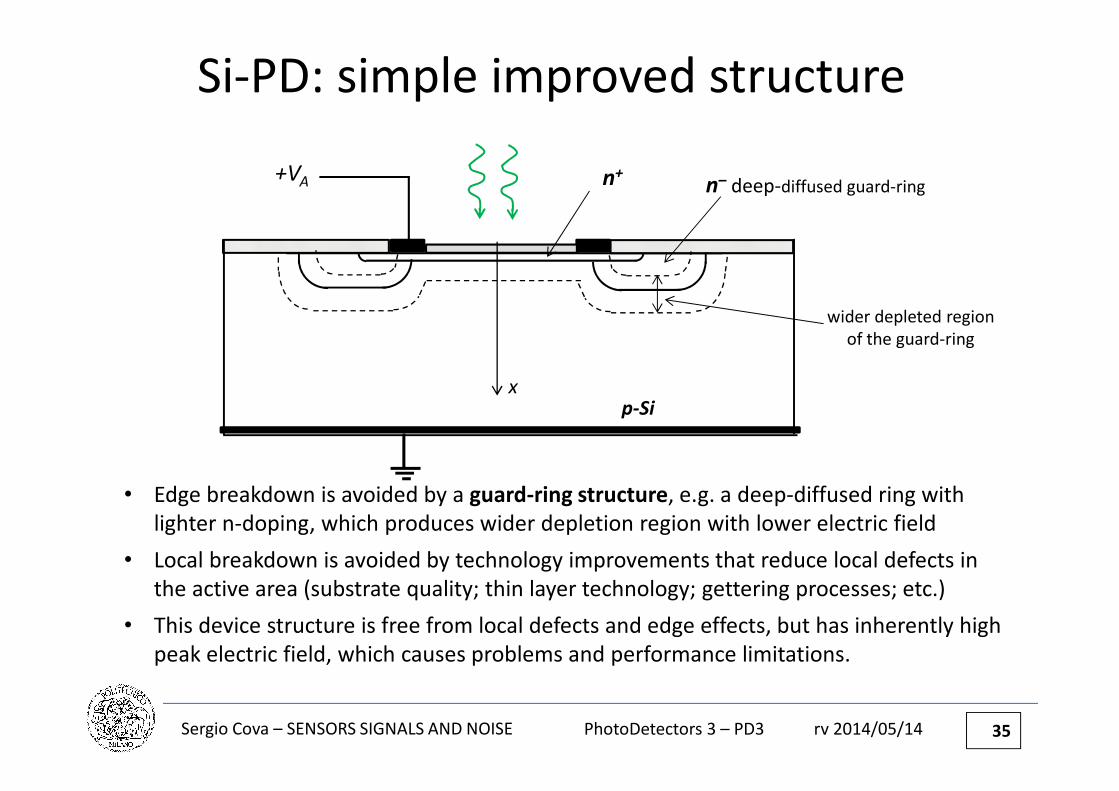
Si-PD: simple improved structure
p-Si
n+
wider depleted region
of the guard-ring
x
+VA n– deep-diffused guard-ring
• Edge breakdown is avoided by a guard-ring structure, e.g. a deep-diffused ring with
lighter n-doping, which produces wider depletion region with lower electric field
• Local breakdown is avoided by technology improvements that reduce local defects in
the active area (substrate quality; thin layer technology; gettering processes; etc.)
• This device structure is free from local defects and edge effects, but has inherently high
peak electric field, which causes problems and performance limitations.
PhotoDetectors 3 – PD3Sergio Cova – SENSORS SIGNALS AND NOISE rv 2014/05/14 36
Problems with the simple Si-PD Structure
The simple improved structure avoids edge effects and local breakdown effects,
but has a disadvantageous electric field profile.
• At the deep boundary of the depletion, the field rises linearly from zero and
remains fairly low in a significant part of the depletion layer. Low field intensity
causes low carrier velocity, which slows down the PD dynamic response
• The electric field has a high peak Edm (twice the average value) that must be
kept below the breakdown level EB (which in Silicon is about 200kV/cm), in
order to avoid an avalanche breakdown that generates a high spurious current.
• For increasing the depletion width wd (in order to improve the detection
efficiency at longer wavelengths) the bias voltage VA must be increased,
thereby increasing also the peak electric field Edm
• Unluckily Edm prematurely attains the breakdown level EB , i.e. before producing
wd adequate for high detection efficiency in the Red and Near InfraRed (NIR)
spectral range.
PhotoDetectors 3 – PD3Sergio Cova – SENSORS SIGNALS AND NOISE rv 2014/05/14 37
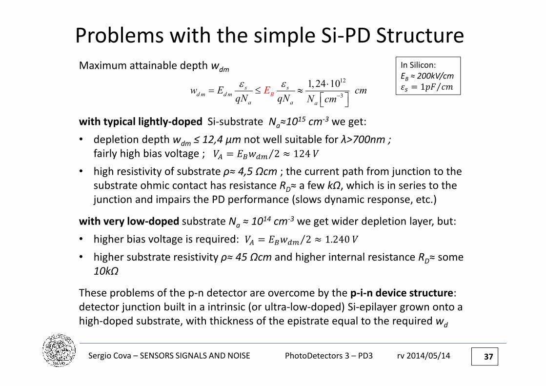
Problems with the simple Si-PD Structure
Maximum attainable depth wdm
with typical lightly-doped Si-substrate Na≈1015 cm-3 we get:
• depletion depth wdm ≤ 12,4 μm not well suitable for λ>700nm ;
fairly high bias voltage ; � = 5���6 2⁄ ≈ 124 �
• high resistivity of substrate ρ≈ 4,5 Ωcm ; the current path from junction to the
substrate ohmic contact has resistance RD≈ a few kΩ, which is in series to the
junction and impairs the PD performance (slows dynamic response, etc.)
with very low-doped substrate Na ≈ 1014 cm-3 we get wider depletion layer, but:
• higher bias voltage is required: � = 5���6 2⁄ ≈ 1.240 �
• higher substrate resistivity ρ≈ 45 Ωcm and higher internal resistance RD≈ some
10kΩ
These problems of the p-n detector are overcome by the p-i-n device structure:
detector junction built in a intrinsic (or ultra-low-doped) Si-epilayer grown onto a
high-doped substrate, with thickness of the epistrate equal to the required wd
12
3
1,24 10s sd m d m
a
B
a a
w E cmq N m
EN q N c
ε ε−
⋅= ≤ ≈
In Silicon:
EB ≈ 200kV/cm
9: = 1#; <=⁄
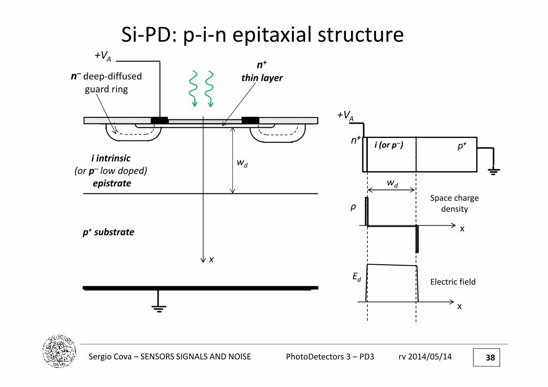
PhotoDetectors 3 – PD3Sergio Cova – SENSORS SIGNALS AND NOISE rv 2014/05/14 38
Si-PD: p-i-n epitaxial structure
p+ substrate
n+
thin layer
x
+VA
n– deep-diffused
guard ring
i intrinsic
(or p-- low doped)
epistrate
n+p+i (or p--)
+VA
x
x
Ed
ρ
wd
Space charge
density
Electric field
wd
PhotoDetectors 3 – PD3Sergio Cova – SENSORS SIGNALS AND NOISE rv 2014/05/14 39
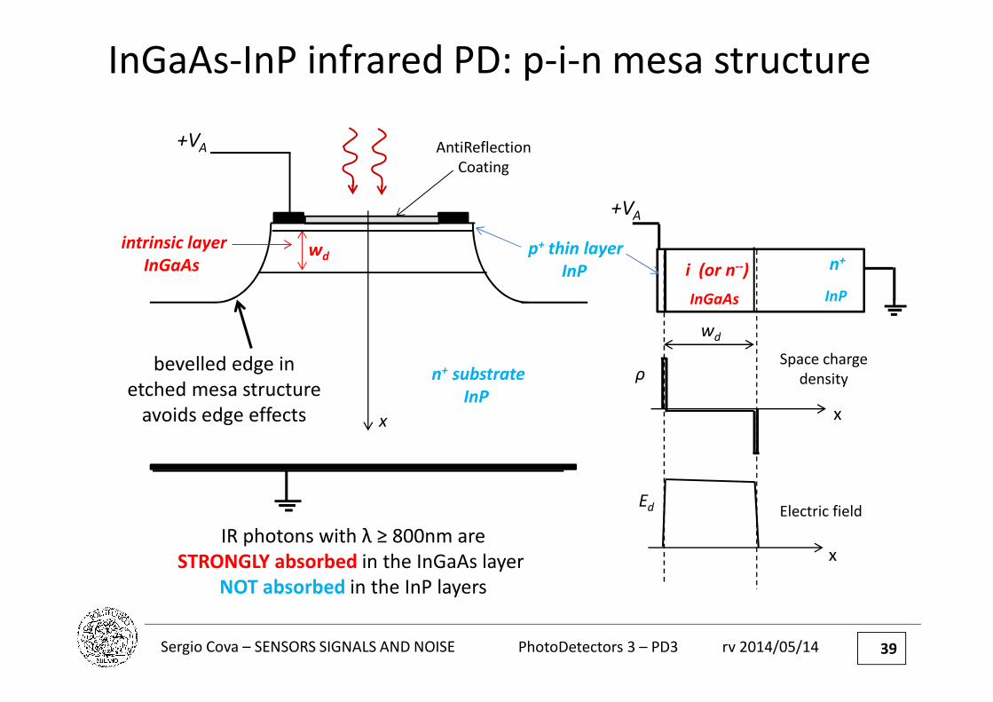
InGaAs-InP infrared PD: p-i-n mesa structure
n+ substrate
InP
x
+VA
n+i (or n--)
+VA
x
x
Ed
ρ
wd
Space charge
density
Electric field
wd
InGaAs
intrinsic layer
InGaAs
InP
bevelled edge in
etched mesa structure
avoids edge effects
p+ thin layer
InP
IR photons with λ ≥ 800nm are
STRONGLY absorbed in the InGaAs layer
NOT absorbed in the InP layers
AntiReflection
Coating


![PD3 & 4 - P c D M c acdn.futureautomation.co.uk/Tech/pd3pd4-instructions.pdf · PD3 - Standard -720mm [28.3”] drop Extra Drop - 1200mm [47.2”] drop PD4 - Bespoke sizes Open position](https://img.pdfslide.us/doc/110x75/6033b80347976733fc75f09a/pd3-4-p-c-d-m-c-acdn-pd3-standard-720mm-283a-drop-extra-drop-.jpg)