Embed Size (px)
Citation preview

The Electrical Engineering HandbookThird Edition
Sensors, Nanoscience,Biomedical Engineering,
and Instruments

The Electrical Engineering Handbook Series
Series Editor
Richard C. DorfUniversity of California, Davis
Titles Included in the Series
The Handbook of Ad Hoc Wireless Networks, Mohammad IlyasThe Avionics Handbook, Cary R. SpitzerThe Biomedical Engineering Handbook, Third Edition, Joseph D. BronzinoThe Circuits and Filters Handbook, Second Edition, Wai-Kai ChenThe Communications Handbook, Second Edition, Jerry GibsonThe Computer Engineering Handbook, Vojin G. OklobdzijaThe Control Handbook, William S. LevineThe CRC Handbook of Engineering Tables, Richard C. DorfThe Digital Signal Processing Handbook, Vijay K. Madisetti and Douglas WilliamsThe Electrical Engineering Handbook, Third Edition, Richard C. DorfThe Electric Power Engineering Handbook, Leo L. GrigsbyThe Electronics Handbook, Second Edition, Jerry C. WhitakerThe Engineering Handbook, Third Edition, Richard C. DorfThe Handbook of Formulas and Tables for Signal Processing, Alexander D. PoularikasThe Handbook of Nanoscience, Engineering, and Technology, William A. Goddard, III,
Donald W. Brenner, Sergey E. Lyshevski, and Gerald J. IafrateThe Handbook of Optical Communication Networks, Mohammad Ilyas and
Hussein T. MouftahThe Industrial Electronics Handbook, J. David IrwinThe Measurement, Instrumentation, and Sensors Handbook, John G. WebsterThe Mechanical Systems Design Handbook, Osita D.I. Nwokah and Yidirim HurmuzluThe Mechatronics Handbook, Robert H. BishopThe Mobile Communications Handbook, Second Edition, Jerry D. GibsonThe Ocean Engineering Handbook, Ferial El-HawaryThe RF and Microwave Handbook, Mike GolioThe Technology Management Handbook, Richard C. DorfThe Transforms and Applications Handbook, Second Edition, Alexander D. PoularikasThe VLSI Handbook, Wai-Kai Chen
The Electrical Engineering HandbookThird Edition
Edited by
Richard C. Dorf
Circuits, Signals, and Speech and Image Processing
Electronics, Power Electronics, Optoelectronics,Microwaves, Electromagnetics, and Radar
Sensors, Nanoscience, Biomedical Engineering,and Instruments
Broadcasting and Optical Communication Technology
Computers, Software Engineering, and Digital Devices
Systems, Controls, Embedded Systems, Energy,and Machines
The Electrical Engineering HandbookThird Edition
Sensors, Nanoscience,Biomedical Engineering,
and Instruments
Edited by
Richard C. DorfUniversity of CaliforniaDavis, California, U.S.A.
A CRC title, part of the Taylor & Francis imprint, a member of theTaylor & Francis Group, the academic division of T&F Informa plc.
Boca Raton London New York

Published in 2006 byCRC PressTaylor & Francis Group 6000 Broken Sound Parkway NW, Suite 300Boca Raton, FL 33487-2742
© 2006 by Taylor & Francis Group, LLCCRC Press is an imprint of Taylor & Francis Group
No claim to original U.S. Government worksPrinted in the United States of America on acid-free paper10 9 8 7 6 5 4 3 2 1
International Standard Book Number-10: 0-8493-7346-8 (Hardcover) International Standard Book Number-13: 978-0-8493-7346-6 (Hardcover) Library of Congress Card Number 2005054343
This book contains information obtained from authentic and highly regarded sources. Reprinted material is quoted withpermission, and sources are indicated. A wide variety of references are listed. Reasonable efforts have been made to publishreliable data and information, but the author and the publisher cannot assume responsibility for the validity of all materialsor for the consequences of their use.
No part of this book may be reprinted, reproduced, transmitted, or utilized in any form by any electronic, mechanical, orother means, now known or hereafter invented, including photocopying, microfilming, and recording, or in any informationstorage or retrieval system, without written permission from the publishers.
For permission to photocopy or use material electronically from this work, please access www.copyright.com(http://www.copyright.com/) or contact the Copyright Clearance Center, Inc. (CCC) 222 Rosewood Drive, Danvers, MA01923, 978-750-8400. CCC is a not-for-profit organization that provides licenses and registration for a variety of users. Fororganizations that have been granted a photocopy license by the CCC, a separate system of payment has been arranged.
Trademark Notice: Product or corporate names may be trademarks or registered trademarks, and are used only foridentification and explanation without intent to infringe.
Library of Congress Cataloging-in-Publication Data
Sensors, nanoscience, biomedical engineering and instruments / edited by Richard C. Dorf.p. cm.
Includes bibliographical references and index.ISBN 0-8493-7346-8 (alk. paper)1. Biosensors. 2. Medical electronics. 3. Biomedical engineering. I. Dorf, Richard C. II. Title.
R857.B54S4555 2005610.28--dc22 2005054343
Visit the Taylor & Francis Web site at http://www.taylorandfrancis.com
and the CRC Press Web site at http://www.crcpress.com
Taylor & Francis Group is the Academic Division of Informa plc.
7346_Discl.fm Page 1 Thursday, November 17, 2005 3:27 PM
Preface
Purpose
The purpose of The Electrical Engineering Handbook, 3rd Edition is to provide a ready reference for the
practicing engineer in industry, government, and academia, as well as aid students of engineering. The third
edition has a new look and comprises six volumes including:
Circuits, Signals, and Speech and Image Processing
Electronics, Power Electronics, Optoelectronics, Microwaves, Electromagnetics, and Radar
Sensors, Nanoscience, Biomedical Engineering, and Instruments
Broadcasting and Optical Communication Technology
Computers, Software Engineering, and Digital Devices
Systems, Controls, Embedded Systems, Energy, and Machines
Each volume is edited by Richard C. Dorf, and is a comprehensive format that encompasses the many
aspects of electrical engineering with articles from internationally recognized contributors. The goal is to
provide the most up-to-date information in the classical fields of circuits, signal processing, electronics,
electromagnetic fields, energy devices, systems, and electrical effects and devices, while covering the emerging
fields of communications, nanotechnology, biometrics, digital devices, computer engineering, systems, and
biomedical engineering. In addition, a complete compendium of information regarding physical, chemical,
and materials data, as well as widely inclusive information on mathematics is included in each volume. Many
articles from this volume and the other five volumes have been completely revised or updated to fit the needs
of today and many new chapters have been added.
The purpose of this volume (Sensors, Nanoscience, Biomedical Engineering, and Instruments) is to provide a
ready reference to subjects in the fields of sensors, materials and nanoscience, instruments and measurements,
and biomedical systems and devices. Here we provide the basic information for understanding these fields. We
also provide information about the emerging fields of sensors, nanotechnologies, and biological effects.
Organization
The information is organized into three sections. The first two sections encompass 10 chapters and the last
section summarizes the applicable mathematics, symbols, and physical constants.
Most articles include three important and useful categories: defining terms, references, and further
information. Defining terms are key definitions and the first occurrence of each term defined is indicated in
boldface in the text. The definitions of these terms are summarized as a list at the end of each chapter or
article. The references provide a list of useful books and articles for follow-up reading. Finally, further
information provides some general and useful sources of additional information on the topic.
Locating Your Topic
Numerous avenues of access to information are provided. A complete table of contents is presented at the
front of the book. In addition, an individual table of contents precedes each section. Finally, each chapter
begins with its own table of contents. The reader should look over these tables of contents to become familiar
with the structure, organization, and content of the book. For example, see Section II: Biomedical Systems,

then Chapter 7: Bioelectricity, and then Chapter 7.2: Bioelectric Events. This tree-and-branch table of contents
enables the reader to move up the tree to locate information on the topic of interest.
Two indexes have been compiled to provide multiple means of accessing information: subject index and
index of contributing authors. The subject index can also be used to locate key definitions. The page on which
the definition appears for each key (defining) term is clearly identified in the subject index.
The Electrical Engineering Handbook, 3rd Edition is designed to provide answers to most inquiries and direct
the inquirer to further sources and references. We hope that this handbook will be referred to often and that
informational requirements will be satisfied effectively.
Acknowledgments
This handbook is testimony to the dedication of the Board of Advisors, the publishers, and my editorial
associates. I particularly wish to acknowledge at Taylor & Francis Nora Konopka, Publisher; Helena Redshaw,
Editorial Project Development Manager; and Susan Fox, Project Editor. Finally, I am indebted to the
support of Elizabeth Spangenberger, Editorial Assistant.
Richard C. DorfEditor-in-Chief
Editor-in-Chief
Richard C. Dorf, Professor of Electrical and Computer Engineering at the University of California, Davis,teaches graduate and undergraduate courses in electrical engineering in the fields of circuits and control
systems. He earned a Ph.D. in electrical engineering from the U.S. Naval Postgraduate School, an M.S. from
the University of Colorado, and a B.S. from Clarkson University. Highly concerned with the discipline of
electrical engineering and its wide value to social and economic needs, he has written and lectured
internationally on the contributions and advances in electrical engineering.
Professor Dorf has extensive experience with education and industry and is professionally active in the fields
of robotics, automation, electric circuits, and communications. He has served as a visiting professor at the
University of Edinburgh, Scotland; the Massachusetts Institute of Technology; Stanford University; and the
University of California, Berkeley.
Professor Dorf is a Fellow of The Institute of Electrical and Electronics Engineers and a Fellow of the
American Society for Engineering Education. Dr. Dorf is widely known to the profession for his Modern
Control Systems, 10th Edition (Addison-Wesley, 2004) and The International Encyclopedia of Robotics (Wiley,
1988). Dr. Dorf is also the co-author of Circuits, Devices and Systems (with Ralph Smith), 5th Edition (Wiley,
1992), and Electric Circuits, 7th Edition (Wiley, 2006). He is also the author of Technology Ventures (McGraw-
Hill, 2005) and The Engineering Handbook, 2nd Edition (CRC Press, 2005).


Advisory Board
Frank BarnesUniversity of Colorado
Boulder, Colorado
Joseph BronzinoTrinity College
Hartford, Connecticut
Wai-Kai ChenUniversity of Illinois
Chicago, Illinois
Delores EtterUnited States Naval Academy
Annapolis, Maryland
Lyle FeiselState University of New York
Binghamton, New York
William KerstingNew Mexico State University
Las Cruces, New Mexico
Vojin OklobdziaUniversity of California, Davis
Davis, California
John V. OldfieldSyracuse University
Syracuse, New York
Banmali RawatUniversity of Nevada
Reno, Nevada
Richard S. SandigeCalifornia Polytechnic
State University
San Luis Obispo, California
Leonard ShawPolytechnic University
Brooklyn, New York
John W. SteadmanUniversity of South Alabama
Mobile, Alabama
R. Lal TummalaMichigan State University
East Lansing, Michigan


Contributors
Ronald ArifLehigh UniversityBethlehem, Pennsylvania
Frank BarnesUniversity of ColoradoBoulder, Colorado
R.C. BarrDuke UniversityDurham, North Carolina
Edward J. BerbariIndiana University/Purdue UniversityIndianapolis, Indiana
Robert A. BondMIT Lincoln LaboratoryLexington, Massachusetts
Joseph D. BronzinoTrinity CollegeHartford, Connecticut
B.S. DhillonUniversity of OttawaOttawa, Ontario, Canada
Alan D. Dorval IIBoston UniversityBoston, Massachusetts
Halit ErenCurtin University of TechnologyBentley, Western Australia, Australia
Martin D. FoxUniversity of ConnecticutStorrs, Connecticut
L.A. GeddesPurdue UniversityLafayette, Indiana
Victor GiurgiutiuUniversity of South CarolinaColumbia, South Carolina
David L. HallThe Pennsylvania State
UniversityUniversity Park, Pennsylvania
Bryan Stewart HobbsCity Technology LimitedPortsmouth, England
Zhian JinLehigh UniversityBethlehem, Pennsylvania
Sam S. KhaliliehTyco Infrastructure ServicesGrand Rapids, Michigan
James LlinasState University of New York
at BuffaloWilliamsville, New York
Sergey Edward LyshevskiRochester Institute of TechnologyRochester, New York
David R. MartinezMIT Lincoln LaboratoryLexington, Massachusetts
M. MeyyappanNASA Ames Research CenterMoffett Field, California
Michael R. NeumanMichigan Technological
UniversityHoughton, Michigan
John PeleskoUniversity of DelawareNewark, Delaware
Yuan PuUniversity of CaliforniaIrvine, California
Christopher G. RelfNational Instruments Certified
LabVIEW DeveloperNew South Wales, Australia
Bonnie Keillor SlatenUniversity of ColoradoBoulder, Colorado
Rosemary L. SmithUniversity of MaineOrono, Maine
Ronald J. TallaridaTemple UniversityPhiladelphia, Pennsylvania
Nelson TansuLehigh UniversityBethlehem, Pennsylvania
Charles W. TherrienNaval Postgraduate SchoolMonterey, California
M. Michael VaiMIT Lincoln LaboratoryLexington, Massachusetts
Joseph WatsonUniversity of WalesSwansea, United Kingdom
John A. WhiteBoston UniversityBoston, Massachusetts
David YoungRockwell Semiconductor SystemsNewport Beach, California


Contents
SECTION I Sensors, Nanoscience, and Instruments
1 Sensors1.1 Introduction Rosemary L. Smith .................................................................................................. 1-1
1.2 Electrochemical Sensors Bryan Stewart Hobbs ......................................................................... 1-11
1.3 The Stannic Oxide Semiconductor Gas Sensor Joseph Watson .............................................. 1-18
2 An Introduction to Multi-Sensor Data Fusion David L. Hall and James Llinas ................ 2-1
3 Magneto-optics David Young and Yuan Pu .................................................................................... 3-1
4 Materials and Nanoscience4.1 Carbon Nanotubes M. Meyyappan .............................................................................................. 4-1
4.2 Modeling MEMS and NEMS John Pelesko ................................................................................. 4-9
4.3 Micromechatronics Victor Giurgiutiu and Sergey Edward Lyshevski ...................................... 4-20
4.4 Nanocomputers, Nano-Architectronics, and Nano-ICs Sergey Edward Lyshevski ................ 4-42
4.5 Semiconductor Nano-Electronics and Nano-Optoelectronics Nelson Tansu,Ronald Arif, and Zhian Jin ............................................................................................................ 4-68
5 Instruments and Measurements5.1 Electrical Equipment in Hazardous Areas Sam S. Khalilieh ..................................................... 5-1
5.2 Portable Instruments and Systems Halit Eren .......................................................................... 5-27
5.3 G (LabVIEWTM) Software Engineering Christopher G. Relf ................................................... 5-36
6 Reliability Engineering B.S. Dhillon ............................................................................................... 6-1
SECTION II Biomedical Systems
7 Bioelectricity7.1 Neuroelectric Principles John A. White and Alan D. Dorval II ................................................ 7-1
7.2 Bioelectric Events L.A. Geddes (revised by R.C. Barr) ............................................................. 7-13
7.3 Biological Effects and Electromagnetic Fields Bonnie Keillor Slaten andFrank Barnes ................................................................................................................................... 7-33
7.4 Embedded Signal Processing David R. Martinez, Robert A. Bond, and M. Michael Vai ..... 7-55

8 Biomedical Sensors Michael R. Neuman ........................................................................................ 8-1
9 Bioelectronics and Instruments9.1 The Electro-encephalogram Joseph D. Bronzino ......................................................................... 9-19.2 The Electrocardiograph Edward J. Berbari ............................................................................... 9-14
10 Tomography Martin D. Fox ............................................................................................................. 10-1
SECTION III Mathematics, Symbols, and Physical Constants
Introduction Ronald J. Tallarida .............................................................................................................. III-1
Greek Alphabet ........................................................................................................................................ III-3International System of Units (SI) ........................................................................................................ III-3Conversion Constants and Multipliers ................................................................................................. III-6Physical Constants ................................................................................................................................... III-8Symbols and Terminology for Physical and Chemical Quantities ..................................................... III-9Credits .................................................................................................................................................... III-13Probability for Electrical and Computer Engineers Charles W. Therrien ..................................... III-14
Indexes
Author Index .................................................................................................................................................... A-1
Subject Index ..................................................................................................................................................... S-1

ISensors, Nanoscience,and Instruments
1 Sensors R.L. Smith, B.S. Hobbs, J. Watson .............................................................................. 1-1Introduction * Electrochemical Sensors * The Stannic Oxide Semiconductor Gas Sensor
2 An Introduction to Multi-Sensor Data Fusion D.L. Hall, J. Llinas ................................... 2-1Introduction * Data Fusion Techniques * Applications of Data Fusion * Process Modelsfor Data Fusion * Limitations of Data Fusion Systems * Summary
3 Magneto-optics D. Young, Y. Pu .............................................................................................. 3-1Introduction * Classification of Magneto-optic Effects * Applications of Magneto-optic Effects
4 Materials and Nanoscience M. Meyyappan, J. Pelesko, V. Giurgiutiu,S.E. Lyshevski, N. Tansu, R. Arif, Z. Jin ...................................................................................... 4-1Carbon Nanotubes * Modeling MEMS and NEMS * Micromechatronics * Nanocomputers,Nano-Architectronics, and Nano-ICs * Semiconductor Nano-Electronicsand Nano-Optoelectronics
5 Instruments and Measurements S.S. Khalilieh, H. Eren, C.G. Relf..................................... 5-1Electrical Equipment in Hazardous Areas * Portable Instruments and Systems *
G (LabVIEWTM) Software Engineering
6 Reliability Engineering B.S. Dhillon ....................................................................................... 6-1Introduction * Terms and Definitions * Bathtub Hazard-Rate Concept * Important Formulas *
Reliability Networks * Reliability Evaluation Methods * Human Reliability * Robot Reliability
I-1

1Sensors
Rosemary L. SmithUniversity of Maine
Bryan Stewart HobbsCity Technology Limited
Joseph WatsonUniversity of Wales
1.1 Introduction ........................................................................ 1-1Physical Sensors * Chemical Sensors * Biosensors * Microsensors
1.2 Electrochemical Sensors....................................................... 1-11Introduction * Potentiometric Sensors * Amperometric Sensors
1.3 The Stannic Oxide Semiconductor Gas Sensor ....................... 1-18Introduction * Basic Electrical Parameters and Operation *
Operating Temperature * Substrate Materials * Electrical Operating
Parameters * Future Developments
1.1 Introduction
Rosemary L. Smith
Sensors are critical components in all measurement and control systems. The need for sensors that generate an
electronic signal closely followed the advent of the microprocessor and computers. Together with the ever-
present need for sensors in science and medicine, the demand for sensors in automated manufacturing and
environmental monitoring is rapidly growing. In addition, small, inexpensive sensors are finding their way
into all sorts of consumer products, from children’s toys to dishwashers to automobiles. Because of the vast
variety of useful things to be sensed and sensor applications, sensor engineering is a multidisciplinary and
interdisciplinary field of endeavor. This chapter introduces some basic definitions, concepts, and features of
sensors, and illustrates them with several examples. The reader is directed to the references and the sources
listed under Further Information for more details and examples.
There are many terms which are often used synonymously for sensor, including transducer, meter, detector,
and gage. Defining the term sensor is not an easy task; however, the most widely used definition is that which has
been applied to electrical transducers by the Instrument Society of America (ANSIMC6.1, 1975): ‘‘Transducer—
A device which provides a usable output in response to a specified measurand.’’ A transducer is more generally
defined as a device which converts energy from one form to another. Usable output can be an optical, electrical,
chemical, or mechanical signal. In the context of electrical engineering, however, a usable output is usually an
electrical signal. The measurand is a physical, chemical, or biological property or condition to be measured.
Most but not all sensors are transducers, employing one or more transduction mechanisms to produce an
electrical output signal. Sometimes sensors are classified as direct or indirect sensors, according to how many
transduction mechanisms are used. For example, a mercury thermometer produces a change in volume of
mercury in response to a temperature change via thermal expansion. The output signal is the change in height
of the mercury column. Here, thermal energy is converted into mechanical movement and we read the change
in mercury height using our eyes as a second transducing element. However, in order to use the thermometer
output in a control circuit or to log temperature data in a computer, the height of the mercury column must
first be converted into an electrical signal. This can be accomplished by several means, but there are more
direct temperature sensing methods, i.e., where an electrical output is produced in response to a change in
temperature. An example is given in the next section on physical sensors. Figure 1.1 depicts a sensor block
1-1
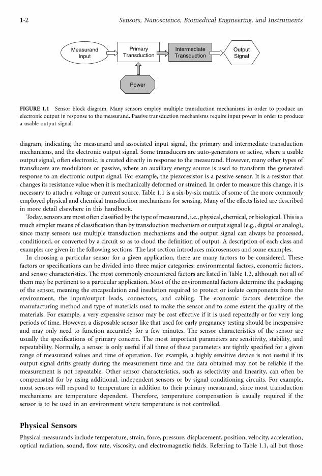
diagram, indicating the measurand and associated input signal, the primary and intermediate transduction
mechanisms, and the electronic output signal. Some transducers are auto-generators or active, where a usable
output signal, often electronic, is created directly in response to the measurand. However, many other types of
transducers are modulators or passive, where an auxiliary energy source is used to transform the generated
response to an electronic output signal. For example, the piezoresistor is a passive sensor. It is a resistor that
changes its resistance value when it is mechanically deformed or strained. In order to measure this change, it is
necessary to attach a voltage or current source. Table 1.1 is a six-by-six matrix of some of the more commonly
employed physical and chemical transduction mechanisms for sensing. Many of the effects listed are described
in more detail elsewhere in this handbook.
Today, sensors aremost often classified by the type ofmeasurand, i.e., physical, chemical, or biological. This is a
much simpler means of classification than by transduction mechanism or output signal (e.g., digital or analog),
since many sensors use multiple transduction mechanisms and the output signal can always be processed,
conditioned, or converted by a circuit so as to cloud the definition of output. A description of each class and
examples are given in the following sections. The last section introduces microsensors and some examples.
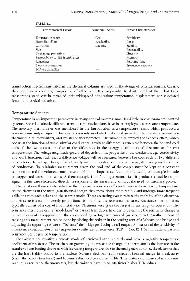
In choosing a particular sensor for a given application, there are many factors to be considered. These
factors or specifications can be divided into three major categories: environmental factors, economic factors,
and sensor characteristics. The most commonly encountered factors are listed in Table 1.2, although not all of
them may be pertinent to a particular application. Most of the environmental factors determine the packaging
of the sensor, meaning the encapsulation and insulation required to protect or isolate components from the
environment, the input/output leads, connectors, and cabling. The economic factors determine the
manufacturing method and type of materials used to make the sensor and to some extent the quality of the
materials. For example, a very expensive sensor may be cost effective if it is used repeatedly or for very long
periods of time. However, a disposable sensor like that used for early pregnancy testing should be inexpensive
and may only need to function accurately for a few minutes. The sensor characteristics of the sensor are
usually the specifications of primary concern. The most important parameters are sensitivity, stability, and
repeatability. Normally, a sensor is only useful if all three of these parameters are tightly specified for a given
range of measurand values and time of operation. For example, a highly sensitive device is not useful if its
output signal drifts greatly during the measurement time and the data obtained may not be reliable if the
measurement is not repeatable. Other sensor characteristics, such as selectivity and linearity, can often be
compensated for by using additional, independent sensors or by signal conditioning circuits. For example,
most sensors will respond to temperature in addition to their primary measurand, since most transduction
mechanisms are temperature dependent. Therefore, temperature compensation is usually required if the
sensor is to be used in an environment where temperature is not controlled.
Physical Sensors
Physical measurands include temperature, strain, force, pressure, displacement, position, velocity, acceleration,
optical radiation, sound, flow rate, viscosity, and electromagnetic fields. Referring to Table 1.1, all but those
PrimaryTransduction
MeasurandInput
OutputSignal
IntermediateTransduction
Power
FIGURE 1.1 Sensor block diagram. Many sensors employ multiple transduction mechanisms in order to produce an
electronic output in response to the measurand. Passive transduction mechanisms require input power in order to produce
a usable output signal.
1-2 Sensors, Nanoscience, Biomedical Engineering, and Instruments
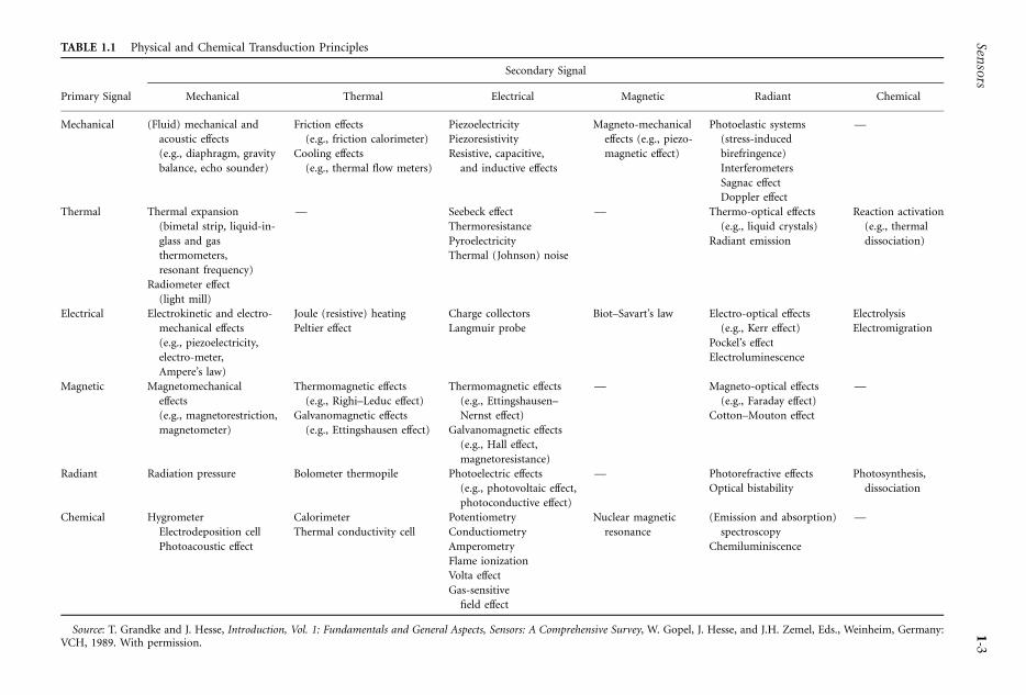
TABLE 1.1 Physical and Chemical Transduction Principles
Secondary Signal
Primary Signal Mechanical Thermal Electrical Magnetic Radiant Chemical
Mechanical (Fluid) mechanical and
acoustic effects
(e.g., diaphragm, gravity
balance, echo sounder)
Friction effects
(e.g., friction calorimeter)
Cooling effects
(e.g., thermal flow meters)
Piezoelectricity
Piezoresistivity
Resistive, capacitive,
and inductive effects
Magneto-mechanical
effects (e.g., piezo-
magnetic effect)
Photoelastic systems
(stress-induced
birefringence)
Interferometers
Sagnac effect
Doppler effect
—
Thermal Thermal expansion
(bimetal strip, liquid-in-
glass and gas
thermometers,
resonant frequency)
Radiometer effect
(light mill)
— Seebeck effect
Thermoresistance
Pyroelectricity
Thermal (Johnson) noise
— Thermo-optical effects
(e.g., liquid crystals)
Radiant emission
Reaction activation
(e.g., thermal
dissociation)
Electrical Electrokinetic and electro-
mechanical effects
(e.g., piezoelectricity,
electro-meter,
Ampere’s law)
Joule (resistive) heating
Peltier effect
Charge collectors
Langmuir probe
Biot–Savart’s law Electro-optical effects
(e.g., Kerr effect)
Pockel’s effect
Electroluminescence
Electrolysis
Electromigration
Magnetic Magnetomechanical
effects
(e.g., magnetorestriction,
magnetometer)
Thermomagnetic effects
(e.g., Righi–Leduc effect)
Galvanomagnetic effects
(e.g., Ettingshausen effect)
Thermomagnetic effects
(e.g., Ettingshausen–
Nernst effect)
Galvanomagnetic effects
(e.g., Hall effect,
magnetoresistance)
— Magneto-optical effects
(e.g., Faraday effect)
Cotton–Mouton effect
—
Radiant Radiation pressure Bolometer thermopile Photoelectric effects
(e.g., photovoltaic effect,
photoconductive effect)
— Photorefractive effects
Optical bistability
Photosynthesis,
dissociation
Chemical Hygrometer
Electrodeposition cell
Photoacoustic effect
Calorimeter
Thermal conductivity cell
Potentiometry
Conductiometry
Amperometry
Flame ionization
Volta effect
Gas-sensitive
field effect
Nuclear magnetic
resonance
(Emission and absorption)
spectroscopy
Chemiluminiscence
—
Source: T. Grandke and J. Hesse, Introduction, Vol. 1: Fundamentals and General Aspects, Sensors: A Comprehensive Survey, W. Gopel, J. Hesse, and J.H. Zemel, Eds., Weinheim, Germany:VCH, 1989. With permission.
1-3
Sensors
transduction mechanisms listed in the chemical column are used in the design of physical sensors. Clearly,
they comprise a very large proportion of all sensors. It is impossible to illustrate all of them, but three
measurands stand out in terms of their widespread application: temperature, displacement (or associated
force), and optical radiation.
Temperature Sensors
Temperature is an important parameter in many control systems, most familiarly in environmental control
systems. Several distinctly different transduction mechanisms have been employed to measure temperature.
The mercury thermometer was mentioned in the Introduction as a temperature sensor which produced a
nonelectronic output signal. The most commonly used electrical signal generating temperature sensors are
thermocouples, thermistors, and resistance thermometers. Thermocouples employ the Seebeck effect, which
occurs at the junction of two dissimilar conductors. A voltage difference is generated between the hot and cold
ends of the two conductors due to the differences in the energy distribution of electrons at the two
temperatures. The voltage magnitude generated depends on the properties of the conductor, e.g., conductivity
and work function, such that a difference voltage will be measured between the cool ends of two different
conductors. The voltage changes fairly linearly with temperature over a given range, depending on the choice
of conductors. To minimize measurement error, the cool end of the couple must be kept at a constant
temperature and the voltmeter must have a high input impedance. A commonly used thermocouple is made
of copper and constantan wires. A thermocouple is an ‘‘auto-generator,’’ i.e., it produces a usable output
signal, in this case electronic, directly in response to the measurand without the need for auxiliary power.
The resistance thermometer relies on the increase in resistance of a metal wire with increasing temperature.
As the electrons in the metal gain thermal energy, they move about more rapidly and undergo more frequent
collisions with each other and the atomic nuclei. These scattering events reduce the mobility of the electrons,
and since resistance is inversely proportional to mobility, the resistance increases. Resistance thermometers
typically consist of a coil of fine metal wire. Platinum wire gives the largest linear range of operation. The
resistance thermometer is a ‘‘modulator’’ or passive transducer. In order to determine the resistance change, a
constant current is supplied and the corresponding voltage is measured (or vice versa). Another means of
making this measurement can be done by placing the resistor in the sensing arm of a Wheatstone bridge and
adjusting the opposing resistor to ‘‘balance’’ the bridge producing a null output. A measure of the sensitivity of
a resistance thermometer is its temperature coefficient of resistance, TCR ¼ (dR/R)(1/dT) in units of percentresistance per degree of temperature.
Thermistors are resistive elements made of semiconductor materials and have a negative temperature
coefficient of resistance. The mechanism governing the resistance change of a thermistor is the increase in the
number of conducting electrons with increasing temperature, due to thermal generation, i.e., the electrons that
are the least tightly bound to the nucleus (valence electrons) gain sufficient thermal energy to break away
(enter the conduction band) and become influenced by external fields. Thermistors are measured in the same
manner as resistance thermometers, but thermistors have up to 100 times higher TCR values.
TABLE 1.2
Environmental Factors Economic Factors Sensor Characteristics
Temperature range Cost Sensitivity
Humidity effects Availability Range
Corrosion Lifetime Stability
Size — Repeatability
Over range protection — Linearity
Susceptibility to EM interferences — Accuracy
Ruggedness — Response time
Power consumption — Frequency response
Self-test capability — —
1-4 Sensors, Nanoscience, Biomedical Engineering, and Instruments
Displacement and Force Sensors
Many types offorces can be sensed by the displacements they create. For example, the force due to acceleration of a
mass at the end of a spring will cause the spring to stretch and the mass to move. Its displacement from the zero
acceleration position is governed by the force generated by the acceleration (F ¼ m · a) and by the restoring force
of the spring. Another example is the displacement of the center of a deformablemembrane due to a difference in
pressure across it. Both of these examples require multiple transduction mechanisms to produce an electronic
output: a primary mechanism which converts force to displacement (mechanical to mechanical) and then an
intermediate mechanism to convert displacement to an electrical signal (mechanical to electrical). Displacement
can be measured by an associated capacitance. For example, the capacitance associated with a gap which is
changing in length is given byC ¼ area · dielectric constant/gap length. The gap must be very small compared
to the surface area of the capacitor, sincemost dielectric constants are of the order of 1 · 10 13 farads/cm andwith
present methods, capacitance is readily resolvable to only about 10 12 farads. This is because measurement leads
and contacts create parasitic capacitances that are of the same order of magnitude. If the capacitance is measured
at the generated site by an integrated circuit, capacitances as small as 10 15 farads can bemeasured. Displacement
is also commonly measured by the movement of a ferromagnetic core inside an inductor coil. The displacement
produces a change in inductance which can be measured by placing the inductor in an oscillator circuit and
measuring the change in frequency of oscillation.
The most commonly used force sensor is the strain gage. It consists of metal wires which are stretched in
response to a force. The resistance of the wire changes as it undergoes strain, i.e., a change in length, since the
resistance of a wire is R ¼ resistivity · length/cross-sectional area. The wire’s resistivity is a bulk property of
the metal which is a constant for constant temperature. A strain gage can be used to measure the force due to
acceleration by attaching both ends of the wire to a cantilever beam (diving board), with one end of the wire at
the attached beam end and the other at the free end. The free end of the cantilever beam moves in response to
acceleration, producing strain in the wire and a subsequent change in resistance. The sensitivity of a strain gage
is described by the unitless gage factor, G ¼ (dR/R)/(dL/L). For metal wires, gage factors typically range from2 to 3. Semiconductors exhibit piezoresistivity, which is a change in resistivity in response to strain.
Piezoresistors have gage factors as high as 130. Piezoresistive strain gages are frequently used in microsensors,
as described later.
Optical Radiation
The intensity and frequency of optical radiation are parameters of great interest and utility in consumer
products such as the video camera and home security systems and in optical communications systems.
Consequently, the technology for optical sensing is highly developed. The conversion of optical energy to
electronic signals can be accomplished by several mechanisms (see radiant to electronic transduction in
Table 1.1); however, the most commonly used is the photogeneration of carriers in semiconductors. The most
often-used device to convert photogeneration to an electrical output is the pn-junction photodiode.
The construction of this device is very similar to the diodes used in electronic circuits as rectifiers. The
photodiode is operated in reverse bias, where very little current normally flows. When light shines on the
structure and is absorbed in the semiconductor, energetic electrons are produced. These electrons flow in
response to the electric field sustained internally across the junction, producing an externally measurable
current (and autogenerator). The current magnitude is proportional to the light intensity and also depends on
the frequency of the light. Figure 1.2 shows the effects of light intensity on the terminal current vs. voltage
behavior of a pn-junction photodiode. Note that for zero applied voltage, a net negative current flows when
the junction is illuminated. This device can therefore also be used as a source of power (a solar cell).
Photodiodes can be made sensitive to specific wavelengths of light by the choice of semiconductor material
and by coating the device with thin film materials which act as optical filters.
Chemical Sensors
Chemical measurands include ion concentration, atomic mass, rate of reactions, reduction-oxidation
potentials, and gas concentration. The last column of Table 1.1 lists some of the transduction mechanisms that
1-5Sensors
have been or could be employed in chemical sensing. Two examples of chemical sensors are described here: the
ion-selective electrode (ISE) and the gas chromatograph. They were chosen because of their general use and
availability, and because they illustrate the use of a primary (ISE) vs. a primary plus intermediate (gas
chromatograph) transduction mechanism.
Ion-Selective Electrode (ISE)
As the name implies, ISEs are used to measure the concentration of a specific ion concentration in a solution
of many ions. To accomplish this, a membrane material is used that selectively generates a potential which is
dependent on the concentration of the ion of interest. The generated potential is usually an equilibrium
potential, called the Nernst potential, and it develops across the interface of the membrane with the solution.
This potential is generated by the initial net flux of ions (charge) across the membrane in response to a
concentration gradient, which generates an electric field that opposes further diffusion. Thenceforth the
diffusional force is balanced by the electric force and equilibrium is established until a change in solution ion
concentration occurs. This equilibrium potential is very similar to the so-called built-in potential of a
pn-junction diode. The ion-selective membrane acts in such a way as to ensure that the generated potential is
dependent mostly on the ion of interest and negligibly on any other ions in solution. This is done by
enhancing the exchange rate of the ion of interest across the membrane, so that it is the fastest moving and,
therefore, the species which generates and maintains the potential.
The most familiar ISE is the pH glass electrode. In this device the membrane is a sodium glass which
possesses a high exchange rate for Hþ. The generated Nernst potential, E, is given by the expression:
E ¼ E0þ(RT/F) ln [Hþ], where E0 is a constant for constant temperature, R is the gas constant, F is the
Faraday constant, and [Hþ] represents the hydrogen ion concentration. The pH is defined as the negative of
the log[Hþ]; therefore, pH ¼ (E0 – E)(log e)(F/RT). One pH unit change corresponds to a tenfold change in
the molar concentration of Hþ and a 59 mV change in the Nernst potential at room temperature. There are
many other ISEs that are commercially available. They have the same type of response, but are sensitive to a
different ion, depending on the membrane material. Some ISEs employ ionophores trapped inside a polymeric
membrane to achieve selectivity. An ionophore is a molecule that selectively and reversibly binds with an ion
and thereby creates a high exchange rate across the membrane that contains it for that particular ion.
−1.E-06
−8.E-07
−6.E-07
−4.E-07
−2.E-07
0.E+00
2.E-07
4.E-07
6.E-07
8.E-07
1.E-06
−1 −0.9 −0.8 −0.7 −0.6 −0.5 −0.4 −0.3 −0.2 −0.1 0 0.1 0.2 0.3 0.4
Volts
Cu
rren
t
increasinglight intensity
FIGURE 1.2 The current vs. voltage characteristics of a semiconductor, pn-junction, photodiode with incident light
intensity.
1-6 Sensors, Nanoscience, Biomedical Engineering, and Instruments

The typical ISE consists of a glass or plastic tube with the ion-selective membrane closing that end of the
tube which is immersed into the solution to be measured. The Nernst potential is measured by making
electrical contact to either side of the membrane. This is done by placing a fixed concentration of
conductive filling solution inside the tube and placing a wire into the solution. The other side of the
membrane is contacted by a reference electrode placed inside the same solution under test. The reference
electrode is constructed in the same manner as the ISE but it has a porous membrane which creates a liquid
junction between its inner filling solution and the test solution. The liquid junction is designed to have a
potential which is invariant with changes in concentration of any ion in the test solution. The reference
electrode, solution under test, and the ISE form an electrochemical cell. The reference electrode
potential acts like the ground reference in electric circuits, and the ISE potential is measured between the
two wires emerging from the respective two electrodes. The details of the mechanisms of transduction in
ISEs are beyond the scope of this chapter. The reader is referred to the texts by Bard and Faulkner (1980)
and Janata (1989).
Gas Chromatograph
Molecules in gases have thermal conductivities which are dependent on their masses; therefore, a pure gas can
be identified by its thermal conductivity. One way to determine the composition of a gas is to first separate it
into its components and then measure the thermal conductivity of each. A gas chromatograph does exactly
that. In a gas-solid chromatograph, the gas flows through a long narrow column which is packed with an
adsorbant solid wherein the gases are separated according to the retentive properties of the packing material
for each gas. As the individual gases exit the end of the tube one at a time, they flow over a heated wire. The
amount of heat transferred to the gas depends on its thermal conductivity. The gas temperature is measured at
a short distance downstream and compared to a known gas flowing in a separate sensing tube. The
temperature of the gas is related to the amount of heat transferred and can be used to derive the thermal
conductivity according to thermodynamic theory and empirical data. This sensor requires two transduction
steps: a chemical to thermal energy transduction followed by a thermal to electrical energy transduction to
produce an electrical output signal.
Biosensors
Biological measurands are biologically produced substances, such as antibodies, glucose, hormones, and
enzymes. Biosensors are not the same as biomedical sensors, which are any sensors used in biomedical
applications, such as blood pressure sensors or electrocardiogram electrodes. Hence, although many
biosensors are biomedical sensors, not all biomedical sensors are biosensors. Table 1.1 does not include
biological signals as a primary signal because they can be generally classified as either biochemical or physical
in nature. Biosensors are of special interest because of the very high selectivity of biological reactions and
binding. However, the detection of that reaction or binding is often elusive. A very familiar commercial
biosensor is the in-home, early pregnancy test, which detects the presence of human growth factor in urine.
That device is a nonelectrical sensor since the output is a color change which our eye senses. In fact, most
biosensors require multiple transduction mechanisms to arrive at an electrical output signal. Two examples as
given below are an immunosensor and an enzyme sensor. Rather than examining a specific species, the
examples describe a general type of sensor and transduction mechanism, since the same principles can be
applied to a very large number of biological species of the same type.
Immunosensor
Commercial techniques for detecting antibody–antigen binding generally utilize optical or x-radiation detection.
An optically fluorescentmolecule or radioisotope is nonspecifically attached to the species of interest in solution.
The complementary binding species is chemically attached to a substrate or beads which are packed into a
column. The tagged solution containing the species of interest, say the antibody, is passed over the antigen-coated
1-7Sensors

surface, where the two selectively bind. After the specific binding occurs, the unbound fluorescent molecules or
radioisotopes are washed away, and the antibody concentration is determined by fluorescence spectroscopy or
with a scintillation counter, respectively. These sensing techniques can be quite costly and bulky, and therefore
other biosensing mechanisms are rapidly being developed. One experimental technique uses the change in the
mechanical properties of the bound antibody–antigen complex in comparison to an unbound surface layer of
antigen. It uses a shearmode, surface acoustic wave (SAW) device (see Ballentine et al., 1997) to sense this change
as a change in the propagation time of the wave between the generating electrodes and the pick-up electrodes
some distance away on the same piezoelectric substrate. The substrate surface is coated with the antigen and it is
theorized that upon selectively binding with the antibody, this layer stiffens, changing the mechanical properties
of the interface and therefore the velocity of the wave. The advantages of this device are that the SAW device
produces an electrical signal (a change in oscillation frequency when the device is used in the feedback loop of an
oscillator circuit) which is dependent on the amount of bound antibody; it requires only a very small amount of
the antigenwhich can be very costly; the entire device is small, robust and portable; and the detection and readout
methods are inexpensive. However, there are numerous problems which currently preclude its widespread,
commercial use, specifically a large temperature sensitivity and responses to nonspecific adsorption, i.e., by
species other than the desired antibody.
Enzyme Sensor
Enzymes selectively react with a chemical substance to modify it, usually as the first step in a chain of reactions
to release energy (metabolism). A well-known example is the selective reaction of glucose oxidase (enzyme)
with glucose to produce gluconic acid and peroxide, according to
C6H12O6 þ O2 !glucose oxidase gluconic acid þ H2O2 þ 80 kilojoules heat
An enzymatic reaction can be sensed by measuring the rise in temperature associated with the heat of reaction
or by the detection and measurement of reaction by-products. In the glucose example, the reaction can be
sensed by measuring the local dissolved peroxide concentration. This is done via an electrochemical analysis
technique called amperometry (Bard and Faulkner, 1980). In this method, a potential is placed across two
inert metal wire electrodes immersed in the test solution and the current which is generated by the reduction/
oxidation reaction of the species of interest is measured. The current is proportional to the concentration of
the reducing/oxidizing species. A selective response is obtained if no other available species has a lower redox
potential. Because the selectivity of peroxide over oxygen is poor, some glucose sensing schemes employ a
second enzyme called catalase which converts peroxide to oxygen and hydroxyl ions. The latter produces a
change in the local pH. As described earlier, an ISE can then be used to convert the pH to a measurable
voltage. In this latter example, glucose sensing involves two chemical-to-chemical transductions followed by a
chemical-to-electrical transduction mechanism.
Microsensors
Microsensors are sensors that are manufactured using integrated circuit fabrication technologies and/or
micromachining. Integrated circuits are fabricated using a series of process steps which are done in batch
fashion meaning that thousands of circuits are processed together at the same time in the same way. The
patterns which define the components of the circuit are photolithographically transferred from a template to
a semiconducting substrate using a photosensitive organic coating, called photoresist. The photoresist
pattern is then transferred into the substrate or into a solidstate thin film coating through an etching or
deposition process. Each template, called a photomask, can contain thousands of identical sets of patterns,
with each set representing a circuit. This ‘‘batch’’ method of manufacturing is what makes integrated circuits
so reproducible and inexpensive. In addition, photoreduction enables one to make extremely small features,
of the order of microns, which is why this collection of process steps is referred to as microfabrication
(Madou, 1997). The resulting integrated circuit is contained in only the top few microns of the
semiconductor substrate and the submicron thin films on its surface. Hence, integrated circuit technology is
said to consist of a set of planar, microfabrication processes. Micromachining refers to the set of processes
1-8 Sensors, Nanoscience, Biomedical Engineering, and Instruments
which produce three-dimensional microstructures using the same photolithographic techniques and batch
processing as for integrated circuits. Here, the third dimension refers to the height above the substrate of the
deposited layer or the depth into the substrate of an etched structure. Micromachining can produce
structures with a third dimension in the range of 1 to 500 microns. The use of microfabrication to
manufacture sensors produces the same benefits as it does for circuits: low cost per sensor, small size, and
highly reproducible features. It also enables the integration of signal conditioning or compensation circuits
and actuators, i.e., entire sensing and control systems, which can dramatically improve sensor performance
for very little increase in cost. For these reasons, there has been a great deal of research and development
activity in microsensors over the past 30 years.
The first microsensors were integrated circuit components, such as semiconductor resistors and pn-junction
diodes. The piezoresistivity of semiconductors and optical sensing by photodiodes were discussed in earlier
sections of this chapter. Junction diodes are also used as temperature sensors. When forward-biased with a
constant diode current, the resulting diode voltage increases approximately linearly with increasing
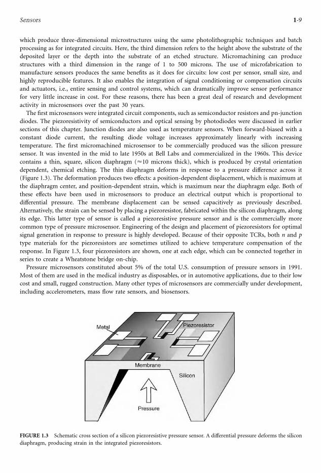
temperature. The first micromachined microsensor to be commercially produced was the silicon pressure
sensor. It was invented in the mid to late 1950s at Bell Labs and commercialized in the 1960s. This device
contains a thin, square, silicon diaphragm (<10 microns thick), which is produced by crystal orientation
dependent, chemical etching. The thin diaphragm deforms in response to a pressure difference across it
(Figure 1.3). The deformation produces two effects: a position-dependent displacement, which is maximum at
the diaphragm center, and position-dependent strain, which is maximum near the diaphragm edge. Both of
these effects have been used in microsensors to produce an electrical output which is proportional to
differential pressure. The membrane displacement can be sensed capacitively as previously described.
Alternatively, the strain can be sensed by placing a piezoresistor, fabricated within the silicon diaphragm, along
its edge. This latter type of sensor is called a piezoresistive pressure sensor and is the commercially more
common type of pressure microsensor. Engineering of the design and placement of piezoresistors for optimal
signal generation in response to pressure is highly developed. Because of their opposite TCRs, both n and p
type materials for the piezoresistors are sometimes utilized to achieve temperature compensation of the
response. In Figure 1.3, four piezoresistors are shown, one at each edge, which can be connected together in
series to create a Wheatstone bridge on-chip.
Pressure microsensors constituted about 5% of the total U.S. consumption of pressure sensors in 1991.
Most of them are used in the medical industry as disposables, or in automotive applications, due to their low
cost and small, rugged construction. Many other types of microsensors are commercially under development,
including accelerometers, mass flow rate sensors, and biosensors.
FIGURE 1.3 Schematic cross section of a silicon piezoresistive pressure sensor. A differential pressure deforms the silicon
diaphragm, producing strain in the integrated piezoresistors.
1-9Sensors

Defining Terms
Micromachining: The set of processes that produces three-dimensional microstructures using sequential
photolithographic pattern transfer and etching or deposition in a batch processing method.
Microsensor: A sensor that is fabricated using integrated circuit and micromachining technologies.
Repeatability: The ability of a sensor to reproduce output readings for the same value of measurand when
applied consecutively and under the same conditions.
Sensitivity: The ratio of the change in sensor output to a change in the value of the measurand.
Sensor: A device that produces a usable output in response to a specified measurand.
Stability: The ability of a sensor to retain its characteristics over a relatively long period of time.
References
ANSI, ‘‘Electrical transducer nomenclature and terminology,’’ ANSI Standard MC6.1–1975 (ISA S37.1),
Research Triangle Park, NC: Instrument Society of America, 1975.
D.S. Ballentine, Jr. et al., Acoustic Wave Sensors: Theory, Design, and Physico-Chemical Applications, San Diego,
CA: Academic Press, 1997.
A.J. Bard and L.R. Faulkner, Electrochemical Methods: Fundamentals and Applications, New York: John Wiley &
Sons, 1980.
R.S.C. Cobbold, Transducers for Biomedical Measurements: Principles and Applications, New York: John Wiley &
Sons, 1974.
W.Gopel, J. Hesse, and J.N. Zemel, ‘‘Sensors: a comprehensive survey,’’ in Fundamentals and General Aspects,
vol. 1, T. Grandke and W.H. Ko, Eds., Weinheim, Germany: VCH, 1989.
J. Janata, Principles of Chemical Sensors, New York: Plenum Press, 1989.
M. Madou, Fundamentals of Microfabrication, Boca Raton, FL: CRC Press, 1997.
Further Information
Sensors: W. Gopel, J. Hesse, and J.N. Zemel, Eds., A Comprehensive Survey, Weinheim, Germany: VCH,
1989–1994.
Vol. 1: Fundamentals and General Aspects, T. Grandke and W.H. Ko, Eds.
Vol. 2, 3, pt. 1–2: Chemical and Biochemical Sensors, W. Gopel et al., Eds.
Vol. 4: Thermal Sensors, T. Ricolfi and J. Scholz, Eds.
Vol. 5: Magnetic Sensors, R. Boll and K.J. Overshott, Eds.
Vol. 6: Optical Sensors, E. Wagner, R. Dandliker, and K. Spenner, Eds.
Vol. 7: Mechanical Sensors, H.H. Bau, N.F. deRooij, and B. Kloeck, Eds.
J. Carr, Sensors and Circuits: Sensors, Transducers, and Supporting Circuits for Electronic Instrumentation,
Measurement, and Control, Englewood Cliffs, NJ: Prentice-Hall, 1993.
J.R. Carstens, Electrical Sensors and Transducers, Englewood Cliffs, NJ: Regents/Prentice-Hall, 1993.
J. Fraden, Handbook of Modern Sensors, 2nd ed., Woodbury, NY: American Institute of Physics Press, 1996.
G.T.A. Kovacs, Micromachined Transducers Sourcebook, McGraw Hill, 1998.
S.M. Sze, Ed., Semiconductor Sensors, NY: John Wiley & Sons, 1994.
D. Tandeske, Pressure Sensors: Selection and Application, New York: Marcel Dekker, 1991.
M.J. Usher and D.A. Keating, Sensors and Transducers: Characteristics, Applications, Instrumentation, Inter-
facing, 2nd ed., New York: Macmillan, 1996.
Sensors and Actuators is a technical journal, published bimonthly by Elsevier Press in two volumes: Vol. A:
Physical Sensors and Actuators, and Vol. B: Chemical Sensors.
The International Conference on Solid-State Sensors and Actuators is held every two years, hosted in rotation
by the U.S., Japan, and Europe. It is sponsored in part by IEEE in the U.S. and a digest of technical
papers is published and available through IEEE.
1-10 Sensors, Nanoscience, Biomedical Engineering, and Instruments

1.2 Electrochemical Sensors
Bryan Stewart Hobbs
Introduction
Electrochemical sensors possess many attractive features which have led to their adoption over a wide range of
applications for detecting and monitoring chemical species, ‘‘analytes,’’ in both the gas and liquid phases. They
are generally available as small, compact, relatively low cost devices, mechanically robust, simple, and reliable
in operation.
A great advantage of electrochemical sensors is that they can operate in ambient temperatures between
about 50–C and þ50–C, without the need for any external heating. Consequently, their power requirementscan be extremely low; some are completely self-powered, additional power only being required for such extra-
sensor functions as alarms, data recording, and transmission, etc. In this respect, electrochemical sensors are
ideally suited to portable instruments where battery power, size, and cost are important considerations. Only
where it is not possible to obtain a satisfactory electrochemical response are cheaper, solid-state,
semiconductor or pellistor devices used instead, for example, in hydrocarbon gas detection.
In fixed instrument applications, where power requirements are a less important criterion, electrochemical
sensors occupy an intermediate position between the comparatively cheaper, but less selective and repeatable,
semiconductor devices and the more sophisticated and complex analytical techniques of optical and mass
spectrometry, chromatography, etc.
Electrochemical sensors divide into two broad categories: ‘‘potentiometric’’ types, producing a voltage
response to an analyte, and ‘‘amperometric’’ sensors, which give an electrical current response. Both sensor
types comprise at least two electrodes, separated by an intervening body of an ionically conducting liquid or
solid electrolyte.
In the majority of electrochemical sensors, the electrolytes used are aqueous solutions of salts, acids, or
bases, and operate at room temperature. However, some specialized products utilize nonaqueous electrolytes
and/or are operated at elevated temperatures. Examples of the latter include solid ceramic electrolyte sensors
based on zirconia which work in environments of several hundreds of degrees centigrade, such as automotive
exhausts and combustion stacks [1]. When operated in normal ambient temperatures, these sensors require
heating via external power supplies, as do semiconductor devices such as the stannic oxide gas sensor.
Potentiometric Sensors
In its simplest form, a potentiometric sensor comprises two electrodes, separated by an electrolyte. The analyte
interacts with one electrode, ‘‘the sensing electrode,’’ so as to establish an ‘‘equilibrium potential’’ at the
interface between the sensing electrode surface and the electrolyte [2]. A second, ‘‘reference electrode,’’ which is
unresponsive to the analyte, establishes a fixed potential with respect to the electrolyte, enabling the sensing
electrode potential to be measured by means of an external voltmeter [3]. Potentiometric measurements are
made under conditions where practically no current flows and voltage measuring circuitry of very high input
impedance is used [4,5].
The voltage output of a potentiometric sensor varies logarithmically with the analyte concentration
according to the so-called Nernst equation [6] which has the general form:
E ¼ E– þ constant ln ½C ð1:1Þ
where E is the measured voltage from the sensor, Eo is the cell voltage under standard conditions [7], and
C is the analyte concentration.
For gases, either in the dissolved or gaseous states, the C term in Equation (1.1) becomes the partial pressure
of the gas.
1-11Sensors
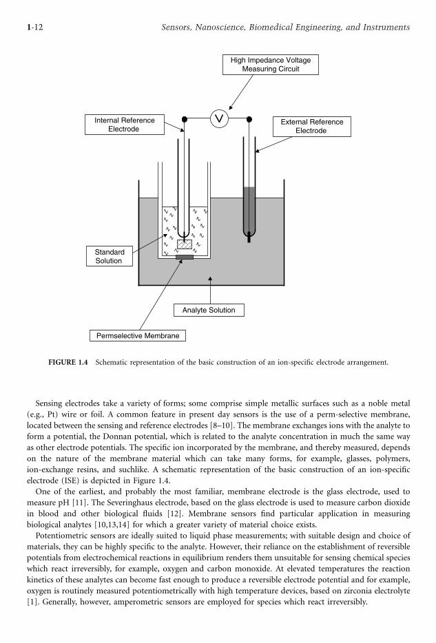
Sensing electrodes take a variety of forms; some comprise simple metallic surfaces such as a noble metal
(e.g., Pt) wire or foil. A common feature in present day sensors is the use of a perm-selective membrane,
located between the sensing and reference electrodes [8–10]. The membrane exchanges ions with the analyte to
form a potential, the Donnan potential, which is related to the analyte concentration in much the same way
as other electrode potentials. The specific ion incorporated by the membrane, and thereby measured, depends
on the nature of the membrane material which can take many forms, for example, glasses, polymers,
ion-exchange resins, and suchlike. A schematic representation of the basic construction of an ion-specific
electrode (ISE) is depicted in Figure 1.4.
One of the earliest, and probably the most familiar, membrane electrode is the glass electrode, used to
measure pH [11]. The Severinghaus electrode, based on the glass electrode is used to measure carbon dioxide
in blood and other biological fluids [12]. Membrane sensors find particular application in measuring
biological analytes [10,13,14] for which a greater variety of material choice exists.
Potentiometric sensors are ideally suited to liquid phase measurements; with suitable design and choice of
materials, they can be highly specific to the analyte. However, their reliance on the establishment of reversible
potentials from electrochemical reactions in equilibrium renders them unsuitable for sensing chemical species
which react irreversibly, for example, oxygen and carbon monoxide. At elevated temperatures the reaction
kinetics of these analytes can become fast enough to produce a reversible electrode potential and for example,
oxygen is routinely measured potentiometrically with high temperature devices, based on zirconia electrolyte
[1]. Generally, however, amperometric sensors are employed for species which react irreversibly.
High Impedance VoltageMeasuring Circuit
External ReferenceElectrode
Analyte Solution
Permselective Membrane
StandardSolution
Internal ReferenceElectrode
FIGURE 1.4 Schematic representation of the basic construction of an ion-specific electrode arrangement.
1-12 Sensors, Nanoscience, Biomedical Engineering, and Instruments

Amperometric Sensors
The amperometric principle can be described in terms of an oxygen sensor by way of example. The cell’s basic
elements comprise at least two electrodes with an intervening body of electrolyte, as for potentiometric
devices. The sensing electrode is made from materials (electrocatalysts) that support the electrochemical
reduction of oxygen, represented by the equation:
O2 þ 2H2Oþ 4e ¼ 4OH ð1:2Þ
Typical materials would be silver, gold, or platinized graphite on a porous PTFE membrane, either as
metallized films or in hydrophobic, gas diffusion, fuel cell electrodes.
The standard reversible potential of this reaction (E–) is 1.229 V at 20–C on the hydrogen scale. However,
due to the irreversible nature of this reaction, even on very active catalysts such as platinum, observed rest
potentials of oxygen electrodes are generally nearer to a volt. Any attempt to draw current from these electrodes
results in sharp polarization of the measured electrode potential, resulting in even lower values.
The counter electrode comprises an anode of a readily corrodible metal such as lead. Lead reacts with
hydroxyl ions (OH ) migrating from the oxygen cathode reaction through the electrolyte and releases
electrons which flow through the external circuit to feed the oxygen reaction:
2Pbþ 4OH ¼ 2PbOþ 2H2Oþ 4e ð1:3Þ
The overall reaction of this metal–air battery cell is given by
2PbþO2 ¼ PbOþ current ð1:4Þ
A large anode surface area, relative to the oxygen cathode, coupled with a low impedance external electrical
circuit connecting the two electrodes, ensures that the lead remains essentially unpolarized and ‘‘holds’’ the
cathode at the lead potential where the oxygen reduction reaction takes place at a high rate.
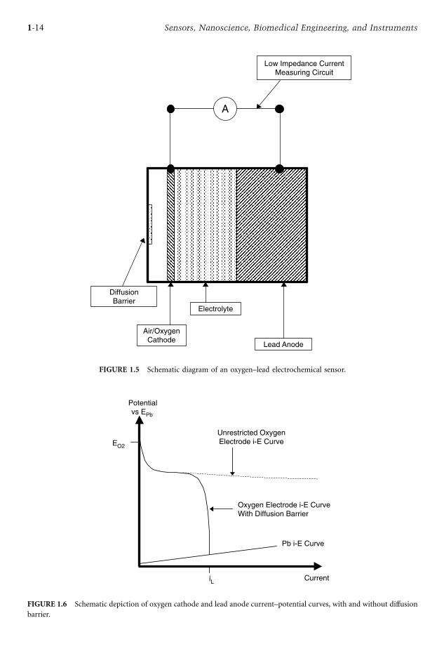
This electrochemical power source is converted to a sensor by the inclusion of a diffusion barrier between
the sensing electrode and its access to the external environment. The barrier restriction is designed to ensure
that the cell operates in the ‘‘diffusion controlled, limiting current condition’’ [15] as illustrated in Figure 1.5
and Figure 1.6.
Operated in this condition, all the oxygen diffusing to the sensing electrode from the external environment
reacts as it arrives at the cathode. The oxygen partial pressure at the cathode will be near zero and the
concentration gradient across the barrier will be equal to the external oxygen partial pressure pO2. From Fick’s
first law of diffusion, it follows that the measured limiting current from the cell, IL will be directly proportional
to the oxygen partial pressure in the external environment [15]:
IL ¼ constantðpO2Þ ð1:5Þ
The nature of the diffusion barrier exerts considerable influence on the sensor characteristics. Early examples
of oxygen sensor, developed by Clark [16,17], employed metallized solid polymer membranes (typically,
PTFE). The gas transport mechanism through these membranes, involving a process of gas dissolution
and diffusion in the solid state, has an inherently high exponential temperature coefficient of about 2% to
3% per –C and temperature compensation is essential. Sensor outputs with these membranes are linear with
pO2.Tantram et al. [15] developed an oxygen sensor based on a porous diffusion barrier, the simplest
form consisting of a single capillary orifice. The gas transport mechanism through porous barriers involves the
physical process of gas-phase diffusion which results in a cell limiting current governed by the following form
1-13Sensors
Low Impedance CurrentMeasuring Circuit
Electrolyte
DiffusionBarrier
Lead Anode
A
Air/OxygenCathode
FIGURE 1.5 Schematic diagram of an oxygen–lead electrochemical sensor.
Unrestricted OxygenElectrode i-E Curve
Pb i-E Curve
Oxygen Electrode i-E CurveWith Diffusion Barrier
Current
Potentialvs EPb
EO2
iL
FIGURE 1.6 Schematic depiction of oxygen cathode and lead anode current–potential curves, with and without diffusion
barrier.
1-14 Sensors, Nanoscience, Biomedical Engineering, and Instruments
of equation
IL ¼ constant:ðT0:5Þ:P 1:pO2 ð1:6Þ
where T is the absolute temperature (K) and P is the total pressure.
The square-root temperature dependence gives coefficient values of about 0.2% per –C, about one tenththat of solid membranes, which considerably reduces the compensation requirements.
The current output is a function of pO2/P, the volume fraction of the gas, rather than the partial pressure.
This provides a signal which is essentially independent of ambient barometric pressure, which is a preferred
characteristic with most gas-phase measurement applications.
Because of bulk flow effects, porous barriers become increasingly nonlinear with increasing gas
concentration [18]. Up to about 20% oxygen, a small secondary correction may be applied to linearize the
output and below a few percent gas analyte, the output is essentially linear.
Sensor life, regardless of diffusion barrier type, will ultimately be determined by the current and the amount
of lead used in these Pb/O2cells. Commercially available cells are capable of two or more years of life in air
(21% oxygen), weigh only a few grams and are about the size of a small alkaline battery cell.
The basic amperometric principle described for oxygen has been adapted to provide sensors for measuring
the concentrations of a range of toxic gases such as CO, H2S, NO, NO2, SO2, and Cl2 [19]. Many of these gases
undergo an electrochemical oxidation at the sensing electrode and an oxygen reducing counter electrode is
used; for example, the electrode reactions for a CO sensor are as follows:
sensing electrode ðCOoxidationÞ 2COþ 2H2O ¼ 2CO2 þ 4Hþ þ 4e ð1:7Þ
counter electrode ðO2 reductionÞ O2 þ 4Hþ þ 4e ¼ 2H2O ð1:8Þ
cell reaction 2COþO2 ¼ 2CO2 þ current ð1:9Þ
The oxygen supply comes from the external environment and such cells operate as self-powered fuel cells.
There are no life-limiting, consumable elements in these toxic gas sensors, in contrast to lead anode in the
Pb/O2 oxygen sensor.
CounterElectrode
iL
SensingElectrode
+
RLoad
RGain
_
OpAmp
| VOut | = RGainiL
FIGURE 1.7 Two-electrode circuit for an amperometric gas sensor.
1-15Sensors
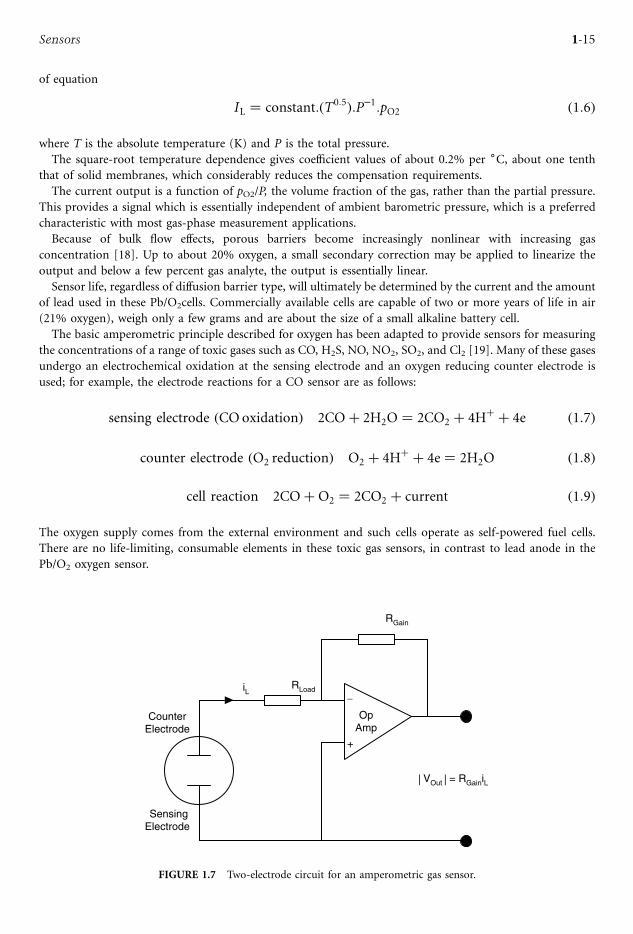
Measurement of the current from a two-electrode amperometric sensor can be accomplished by simply
measuring the voltage across a low value resistor connecting the electrodes. Alternatively, a potentiostatic
circuit can be used, which consumes very little external power and enables the cell to run at an effectively zero
load resistance [4,20] (Figure 1.7). This circuit yields a faster response and reduces polarization effects from
the oxygen counter electrode in toxic gas sensors which tend to destabilize the signal.
| VOut | = RLoadiL
iL
RLoad
+
_
OpAmp
CounterElectrode
SensingElectrode
ReferenceElectrode
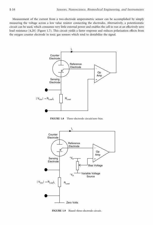
FIGURE 1.8 Three-electrode circuit/zero bias.
iL
RLoad| VOut | = RLoadiL
+
_
OpAmp
CounterElectrode
SensingElectrode
ReferenceElectrode
Variable VoltageSource
Zero Volts
+VR
−VR
Bias Voltage
FIGURE 1.9 Biased three-electrode circuit.
1-16 Sensors, Nanoscience, Biomedical Engineering, and Instruments

Most toxic sensors are operated with a third, reference electrode and an external three-electrode
potentiostatic circuit (Figure 1.8). The reference electrode is normally formed by an additional, oxygen-
responsive counter electrode from which no current is drawn. The potentiostat in Figure 1.8 operates to
‘‘hold’’ the sensing electrode at the reference electrode potential. The cell current, passing between counter and
sensing electrodes, is measured in the amplifier feedback loop to eliminate completely all polarization effects
within the cell [4,5,20].
Three-electrode circuits also allow the possibility of ‘‘biasing’’ the sensing electrode operating potential with
respect to the reference electrode as depicted in Figure 1.9, thus giving more flexibility in choosing optimal
operating potentials for the analyte and/or suppressing cross interfering gas reactions [20].
References
1. W.C. Maskell, Techniques and Mechanisms in Gas Sensing, P.T. Moseley, J.O.W. Norris, D.E. Williams,
Eds., IOP Publishing, 1991, pp. 1–42.
2. C.W. Davies and A.M. James, A Dictionary of Electrochemistry, New York: Macmillan Press, 1976, pp. 86–
89 (see also pp. 92–96).
3. D.J.G. Ives and G.J. Janz, Reference Electrodes, Theory and Practice, London: Academic Press, 1961.
4. D.T. Sawyer and J.L. Roberts, Experimental Electrochemistry for Chemists, New York: Wiley, 1974,
Chap. 5.
5. M.J.D. Brand and B. Fleet, ‘‘Operational amplifiers in chemical instrumentation,’’ Chem. Br., vol. 5,
no. 12, pp. 557–562, 1969.
6. C.W. Davies and A.M. James, A Dictionary of Electrochemistry, New York: Macmillan Press, 1976,
p. 168.
7. C.W. Davies and A.M. James, A Dictionary of Electrochemistry, New York: Macmillan Press, 1976, p. 87.
8. C.W. Davies and A.M. James, A Dictionary of Electrochemistry, New York: Macmillan Press, 1976,
pp. 150–153.
9. M.J. Madou and S.R. Morrison, Chemical Sensing with Solid State Devices, London: Academic Press,
1989, Chap. 6.
10. D.J.G. Ives and G.J. Janz, Reference Electrodes, Theory and Practice, London: Academic Press, 1961,
Chap. 9.
11. D.J.G. Ives and G.J. Janz, Reference Electrodes, Theory and Practice, London: Academic Press, 1961,
Chap. 5.
12. D.J.G. Ives and G.J. Janz, Reference Electrodes, Theory and Practice, London: Academic Press, 1961,
pp. 497–501.
13. D.J.G. Ives and G.J. Janz, Reference Electrodes, Theory and Practice, London: Academic Press, 1961,
Chap. 11.
14. A.P.F. Turner, I. Karube and G.S. Wilson, Eds., Biosensors, Fundamentals and Applications, Oxford:
Oxford University Press, 1987.
15. A.D.S. Tantram, M.J. Kent, and A.G. Palmer, U.K. Patent 1571282, 1977.
16. D.T. Sawyer and J.L. Roberts, Experimental Electrochemistry for Chemists, New York: Wiley, 1974,
pp. 383–384.
17. L.C. Clark Jr., Trans. Am. Soc. Artif. Intern. Organs, 2, 41, 1956.
18. B.S. Hobbs, A.D.S. Tantram, and R. Chan-Henry, Techniques and Mechanisms in Gas Sensing,
P.T. Moseley, J.O.W. Norris, and D.E. Williams, Eds., IOP Publishing, 1991, pp. 171–172.
19. A.D.S. Tantram, J.R. Finbow, Y.S. Chan, and B.S. Hobbs, U.K. Patent 2094005, 1982.
20. B.S. Hobbs, A.D.S. Tantram, and R. Chan-Henry; Techniques and Mechanisms in Gas Sensing,
P.T. Moseley, J.O.W. Norris, and D.E. Williams, Eds., IOP Publishing, 1991, pp. 180–183.
1-17Sensors
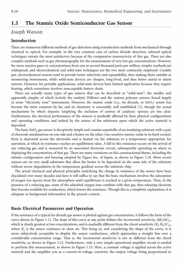
1.3 The Stannic Oxide Semiconductor Gas Sensor
Joseph Watson
Introduction
There are numerous different methods of gas detection using transduction methods from mechanical through
chemical to optical. For example, in the very common case of carbon dioxide detection, infrared optical
techniques remain the most satisfactory because of the comparative nonreactivity of that gas. There are also
complex methods such as gas chromatography for the measurement of very low gas concentrations. However,
for more reactive gases in concentrations from one to several thousand parts per million, simpler methods are
widespread, and electrochemical and solid-state techniques are the two most commonly employed. Crudely
put, electrochemical sensors tend to provide better selectivity and repeatability, thus making them suitable as
monitoring instruments, while solid-state devices are cheaper, long-lived, and thus better suited to alarm
systems. However, for portable applications, solid-state devices have limited application because they require
heating, which sometimes involves unacceptable battery drain.
There are actually many types of gas sensors that can be described as ‘‘solid-state’’, the smaller and
apparently simpler of which include the catalytic Pellistor and the various polymer sensors found largely
in some ‘‘electronic nose’’ instruments. However, the stannic oxide (i.e., tin dioxide, or SnO2) sensor has
become the most common by far, and its chemistry is reasonably well established [1], though the actual
mechanisms by which dopants (implying the inclusion of centres of catalysis) operate are less clear.
Furthermore, the electrical performance of the sensors is markedly affected by their physical configurations
and operating conditions and indeed by the nature of the substrates upon which the active material is
deposited.
The basic SnO2 gas sensor is deceptively simple and consists essentially of an insulating substrate with a pair
of electrode metalizations on one side and a heater on the other. Gas-sensitive stannic oxide in its hard ceramic
form is deposited across the electrodes and is heated via the substrate to a temperature appropriate for
operation, at which its resistance reaches an equilibrium value. A fall in this resistance occurs on the arrival of
any reducing gas and is measured by an associated electronic circuit, subsequently operating an alarm or
displaying the concentration of that gas. There are many variations on this constructional theme, including the
tubular configuration and housing adopted by Figaro Inc. of Japan, as shown in Figure 1.10. More recent
sensors are on very small substrates that allow the heater to be deposited on the same side of the substrate
without severe degradation in the temperature gradient across the substrate chip.
The actual chemical and physical principles underlying the change in resistance of the sensor have been
elucidated over many decades and here it will suffice to say that the basic mechanism involves the adsorption
of oxygen ion species from the atmosphere until equilibrium is reached at a given temperature. Then, in the
presence of a reducing gas, some of the adsorbed oxygen ions combine with that gas, thus releasing electrons
that become available for conduction, which lowers the resistance. Though this is a simplistic explanation, it is
adequate as background information in the present context.
Basic Electrical Parameters and Operation
If the resistance of a typical tin dioxide gas sensor is plotted against gas concentration, it follows the form of the
curve shown in Figure 1.11. The slope of this curve at any point defines the incremental sensitivity, DRS/DCG,which is clearly greatest at low concentrations, and is markedly different from the chord sensitivity (Ra-RS)/CG,
where Ra is the sensor resistance in clean air. This being so, and considering the shape of the curve, it is
more subjectively acceptable to display the sensor conductance, which approaches a straight line over a
considerable concentration range. That is, the incremental sensitivity is not so different from the chord
sensitivity, as shown in Figure 1.12. Furthermore, only a very simple operational amplifier circuit is needed
to perform this measurement, as shown in Figure 1.13. Here, a constant voltage is applied across the active
material and the amplifier acts as a current-to-voltage converter, the output voltage being proportional to
1-18 Sensors, Nanoscience, Biomedical Engineering, and Instruments
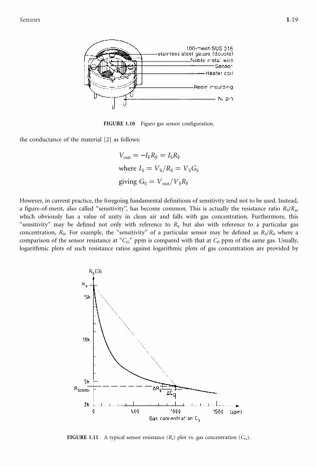
the conductance of the material [2] as follows:
Vout ¼ IFRF ¼ ISRF
where IS ¼ VS=RS ¼ VSGS
giving GS ¼ Vout=VSRF
However, in current practice, the foregoing fundamental definitions of sensitivity tend not to be used. Instead,
a figure-of-merit, also called ‘‘sensitivity’’, has become common. This is actually the resistance ratio RS/Ra,
which obviously has a value of unity in clean air and falls with gas concentration. Furthermore, this
‘‘sensitivity’’ may be defined not only with reference to Ra but also with reference to a particular gas
concentration, R0. For example, the ‘‘sensitivity’’ of a particular sensor may be defined as RS/R0 where a
comparison of the sensor resistance at ‘‘CG’’ ppm is compared with that at C0 ppm of the same gas. Usually,
logarithmic plots of such resistance ratios against logarithmic plots of gas concentration are provided by
FIGURE 1.10 Figaro gas sensor configuration.
FIGURE 1.11 A typical sensor resistance (Rs) plot vs. gas concentration (CG).
1-19Sensors
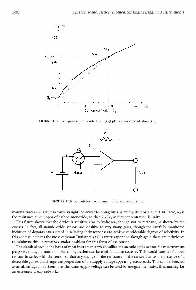
manufacturers and result in fairly straight, downward-sloping lines as exemplified by Figure 1.14. Here, R0 is
the resistance at 250 ppm of carbon monoxide, so that RS/Rx0 at that concentration is unity.
This figure shows that the device is sensitive also to hydrogen, though not to methane, as shown by the
crosses. In fact, all stannic oxide sensors are sensitive to very many gases, though the carefully monitored
inclusion of dopants can succeed in tailoring their responses to achieve considerable degrees of selectivity. In
this context, perhaps the most common ‘‘nuisance gas’’ is water vapor and though again there are techniques
to minimize this, it remains a major problem for this form of gas sensor.
The circuit shown is the basis of most instruments which utilize the stannic oxide sensor for measurement
purposes, though a much simpler configuration can be used for alarm systems. This would consist of a load
resistor in series with the sensor so that any change in the resistance of the sensor due to the presence of a
detectable gas would change the proportion of the supply voltage appearing across each. This can be detected
as an alarm signal. Furthermore, the same supply voltage can be used to energize the heater, thus making for
an extremely cheap network.
FIGURE 1.12 A typical sensor conductance (GS) plot vs. gas concentration (CG).
FIGURE 1.13 Circuit for measurement of sensor conductance.
1-20 Sensors, Nanoscience, Biomedical Engineering, and Instruments
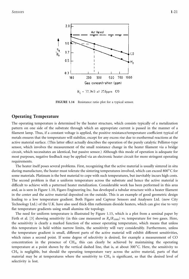
Operating Temperature
The operating temperature is determined by the heater structure, which consists typically of a metalization
pattern on one side of the substrate through which an appropriate current is passed in the manner of a
filament lamp. Thus, if a constant voltage is applied, the positive resistance/temperature coefficient typical of
metals ensures that the temperature will stabilize, except for any excess rise due to exothermal reactions at the
active material surface. (This latter effect actually describes the operation of the purely catalytic Pellistor-type
sensor, which involves the measurement of the small resistance change in the heater filament via a bridge
circuit, which necessitates an identical, but passive sensor.) Although this mode of operation is adequate for
most purposes, negative feedback may be applied via an electronic heater circuit for more stringent operating
requirements.
The heater itself poses several problems. First, recognizing that the active material is usually sintered in situ
during manufacture, the heater must tolerate the sintering temperatures involved, which can exceed 800–C forsome materials. Platinum is the best material to cope with such temperatures, but inevitably incurs high costs.
The second problem is that a uniform temperature across the substrate and hence the active material is
difficult to achieve with a patterned heater metalization. Considerable work has been performed in this area
and, as is seen in Figure 1.10, Figaro Engineering Inc. has developed a tubular structure with a heater filament
in the center and the active material deposited on the outside. This is an example of good geometric design
leading to a low temperature gradient. Both Figaro and Capteur Sensors and Analysers Ltd. (now City
Technology Ltd.) of the U.K. have also used thick-film ruthenium dioxide heaters, which can give rise to very
flat temperature gradients using small alumina tile topology.
The need for uniform temperature is illustrated by Figure 1.15, which is a plot from a seminal paper by
Firth et al. [3] showing sensitivity (in this case measured as Ra/R1000) vs. temperature for two gases. Here,
the sensitivity is clearly a marked function of the sensor operating temperature, which means that unless
this temperature is held within narrow limits, the sensitivity will vary considerably. Furthermore, unless
the temperature gradient is small, different parts of the active material will exhibit different sensitivities,
which raises a second point. If some degree of selectivity is desired, for example a measurement of CO
concentration in the presence of CH4, this can clearly be achieved by maintaining the operating
temperature at a point shown by the vertical dashed line, that is, at about 300–C. Here, the sensitivity toCH4 is negligible, but should the operating temperature vary across the active material, parts of that
material may be at temperatures where the sensitivity to CH4 is significant, so that the desired level of
selectivity is lost.
FIGURE 1.14 Resistance ratio plot for a typical sensor.
1-21Sensors
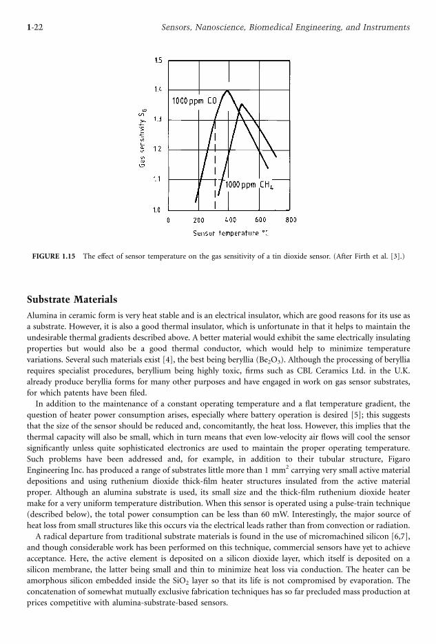
Substrate Materials
Alumina in ceramic form is very heat stable and is an electrical insulator, which are good reasons for its use as
a substrate. However, it is also a good thermal insulator, which is unfortunate in that it helps to maintain the
undesirable thermal gradients described above. A better material would exhibit the same electrically insulating
properties but would also be a good thermal conductor, which would help to minimize temperature
variations. Several such materials exist [4], the best being beryllia (Be2O3). Although the processing of beryllia
requires specialist procedures, beryllium being highly toxic, firms such as CBL Ceramics Ltd. in the U.K.
already produce beryllia forms for many other purposes and have engaged in work on gas sensor substrates,
for which patents have been filed.
In addition to the maintenance of a constant operating temperature and a flat temperature gradient, the
question of heater power consumption arises, especially where battery operation is desired [5]; this suggests
that the size of the sensor should be reduced and, concomitantly, the heat loss. However, this implies that the
thermal capacity will also be small, which in turn means that even low-velocity air flows will cool the sensor
significantly unless quite sophisticated electronics are used to maintain the proper operating temperature.
Such problems have been addressed and, for example, in addition to their tubular structure, Figaro
Engineering Inc. has produced a range of substrates little more than 1 mm2 carrying very small active material
depositions and using ruthenium dioxide thick-film heater structures insulated from the active material
proper. Although an alumina substrate is used, its small size and the thick-film ruthenium dioxide heater
make for a very uniform temperature distribution. When this sensor is operated using a pulse-train technique
(described below), the total power consumption can be less than 60 mW. Interestingly, the major source of
heat loss from small structures like this occurs via the electrical leads rather than from convection or radiation.
A radical departure from traditional substrate materials is found in the use of micromachined silicon [6,7],
and though considerable work has been performed on this technique, commercial sensors have yet to achieve
acceptance. Here, the active element is deposited on a silicon dioxide layer, which itself is deposited on a
silicon membrane, the latter being small and thin to minimize heat loss via conduction. The heater can be
amorphous silicon embedded inside the SiO2 layer so that its life is not compromised by evaporation. The
concatenation of somewhat mutually exclusive fabrication techniques has so far precluded mass production at
prices competitive with alumina-substrate-based sensors.
FIGURE 1.15 The effect of sensor temperature on the gas sensitivity of a tin dioxide sensor. (After Firth et al. [3].)
1-22 Sensors, Nanoscience, Biomedical Engineering, and Instruments
Electrical Operating Parameters
In addition to new departures in substrate materials and geometry, there are various methods of electrical
control and measurement, usually involving pulsed as opposed to continuous operation [8]. There are several
reasons for this, as follows.
The first is a requirement for low power consumption, thereby making battery operation more feasible. If a
sensor is sufficiently small — that is, it has a very low thermal capacity — it may be driven up to its optimum
operating temperature within a few milliseconds. So, keeping in mind that contaminant gas concentrations do
not change significantly in so short a time, the sensor can be operated intermittently instead of continuously.
A case in point is that of the Figaro type 2440, which has a very small structure. This sensor is operated by
applying a 5 V heater supply for 14 msec followed by a ‘‘resting’’ period of 236 msec that is, a duty cycle of
nearly 1:18. This results in an average power consumption lower than 60 mW. During every fourth ‘‘resting’’
period, the active material is interrogated by a 5 V pulse lasting some 5 msec. That is, the read-out is updated
on a one-second basis, which is much less than the time taken for an atmospheric carbon monoxide
concentration to change significantly.
Second, if the optimum operating temperature of a sensor is low — typically about 100–C for CO-selectivetypes — water vapor and trace concentrations of pollutant gases in the atmosphere can temporarily poison
that sensor. However, if the temperature is increased to well above the operating level, such contaminants can
usually be removed — a process known as ‘‘purging’’. So, one method of operation is to sequentially heat the
sensor to a high temperature for this purpose, allow it to cool to its optimum operating temperature, then to
make an electrical measurement. The Figaro TGS 2440 again affords an example of this. The 14 msec heating
pulse is actually long enough to bring the temperature to more than 300–C and this falls to the optimum
measuring temperature some 150 msec later, which is when the interrogation pulse arrives. It should be noted
that for this mode of operation, materials must be selected very carefully for the various parts of the sensor
structure because the whole assembly must withstand a continuing sequence of thermal shocks over many
years without damage.
Third, a comparatively new modus operandi involves the measurement of conductance rise-times upon
application of the polarizing voltage across the active material. In this method, the sensor is maintained at the
optimum operating temperature and a fast rise-time polarizing voltage is applied. The resulting active material
conductance change has been shown to be dependent upon the gas concentration. Furthermore, there is
evidence that the rise-times may also provide gas recognition information [9].
Future Developments
Considerable progress in the chemistry and physics of the active material is currently ongoing. A good
illustration is the use of nano-particles along with pulsed-operation techniques [10]. The use of stannic oxide
sensors in arrays with each member having different characteristics has also received attention in the context of
‘‘electronic nose’’ technology [11,12]. Here, sophisticated computer techniques have been used to derive both
qualitative and quantitative information about mixtures of gases using sensors that have overlapping
selectivity and sensitivity characteristics. It has therefore become clear that although the stannic oxide gas
sensor has achieved prominence in mass-produced and inexpensive devices such as domestic gas alarms, it is a
viable sensor for measurement and monitoring instruments and has by no means reached the limit of its
capabilities.
References
1. K. Ihokura and J. Watson, The Stannic Oxide Gas Sensor, Boca Raton, FL: CRC Press, 1994.
2. J. Watson, ‘‘A note on the characterisation of gas sensors,’’ Sens. Actuators, B8, 173–177, 1992.
3. J.G. Firth, A. Jones, and T.A. Jones, ‘‘Solid-state detectors for carbon monoxide,’’ Ann. Occup. Hyg. 18,
63–68, 1975.
4. M.P. Elwin, G.S.V. Coles, and J. Watson, ‘‘New substrates for thick and thin film gas sensors,’’ Sens. Appl.
Conf. VII, 37–42, 1996.
1-23Sensors

5. D.M. Wilson, S. Hoyt, J. Janata, K. Booksh, and L. Ohando, ‘‘Chemical sensors for portable handheld
instruments,’’ IEEE Sens. J., vol. 1, no. 4, pp. 256–273, 2001.
6. D. Mutschall, C. Scheibe and E. Obermeier, ‘‘Basic micromodule for chemical sensors with on-chip
heater and buried sensor structure,’’ 8th Int. Conf. Solid-state Sens. Actuators Eurosensors IX, Stockholm,
1995.
7. G.G. Mandayo, E. Castano and F.J. Gracia, ‘‘Carbon monoxide detector fabricated on the basis of a tin
oxide novel doping method,’’ IEEE Sens. J., vol. 2, no. 4, pp. 322–328, 2002.
8. T. Amamoto, Tamaguchi, Y. Matsuura and Y. Kajiyama, ‘‘Development of pulse-drive semiconductor gas
sensor,’’ Sens. Actuators, B13/14, 587–588, 1993.
9. E. Llobet, X. Vilanova, J. Brezmes, J.E. Sueiras, and X. Correig, ‘‘Transient response of thick film tin
oxide gas sensors to multicomponent gas mixtures,’’ Sens. Actuators B, vol. 47, no. 1-3, pp. 104–112,
1998.
10. T.K.H. Starke and G.S.V. Coles, ‘‘Reduced response times using adsorption kinetics and pulsed-mode
operation for the detection of oxides of nitrogen with nanocrystalline SnO2 sensors,’’ IEEE Sens. J., vol.
3, no. 4, pp. 447–453, 2003.
11. I. Sagayo, Md. C. Horvillo, S. Baluk, M. Alexandre, M.J. Fernandez, L. Ares, M. Garcia, J.P. Santos, and
J. Gutierrez, ‘‘Detection of toxic gases by a tin oxide multisensor,’’ IEEE Sens. J., vol. 2, no. 5, pp. 387–
393, 2002.
12. D.S. Lee, D.D. Lee, S.W. Ban, M.H. Lee, and Y.T. Kim, ‘‘SnO2 gas sensing array for combustible and
explosive gas leakage recognition,’’ IEEE Sens. J. vol. 2, no. 3, pp. 140–149, 2002.
1-24 Sensors, Nanoscience, Biomedical Engineering, and Instruments

2An Introduction toMulti-Sensor Data
Fusion1
David L. HallThe Pennsylvania State University
James LlinasState University of New York at
Buffalo
2.1 Introduction ........................................................................ 2-1
2.2 Data Fusion Techniques ........................................................ 2-3
2.3 Applications of Data Fusion................................................... 2-5
2.4 Process Models for Data Fusion ............................................. 2-7
2.5 Limitations of Data Fusion Systems ...................................... 2-12
2.6 Summary .......................................................................... 2-13
2.1 Introduction
Multi-sensor data fusion involves combining information and data from multiple sources to obtain the most
accurate and specific assessment of an observed environment or situation [1–6]. Examples of data fusion
applications include monitoring the health of a complex machine [7], use of multiple sources to improve
medical diagnosis [8], automated target recognition for military applications [9], and environmental
monitoring [10]. Automated data fusion systems seek to emulate the ability of humans and animals to
improve their assessment of the external world by integrating information from multiple senses. Techniques
for automated data fusion range from signal processing and image processing techniques, to statistical based
estimation (e.g., Kalman filters), pattern recognition methods (cluster algorithms and adaptive neural
networks), voting, Bayesian and Dempster–Shafer methods, to automated reasoning techniques such as
expert systems, fuzzy logic, blackboard systems, and intelligent agents. An overview of these methods is
provided by Hall and McMullen [1] and Waltz and Llinas [2]. This chapter provides an introduction to
multi-sensor data fusion including the basic concepts, models, and processing architectures, algorithms and
techniques, and applications. A brief discussion of the state of the art of data fusion is provided at the end of
the chapter.
Data fusion mimics the human cognitive process involving integrating sensory data to understand the
external world. Humans receive and process sensory data (sights, sounds, smells, tastes, and touch) that
are assessed to draw conclusions about the environment and what it means. The development of data
1Note: While this is original material, it is based on a previous introduction to multi-sensor data fusion provided by Hall and
Llinas [6] and by Hall and McMullen [1].
2-1
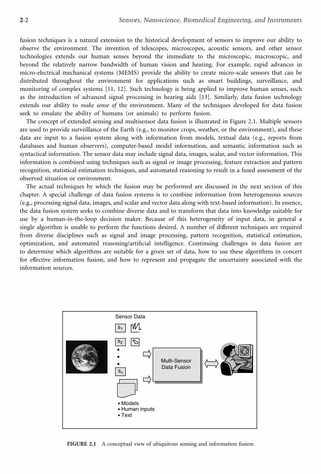
fusion techniques is a natural extension to the historical development of sensors to improve our ability to
observe the environment. The invention of telescopes, microscopes, acoustic sensors, and other sensor
technologies extends our human senses beyond the immediate to the microscopic, macroscopic, and
beyond the relatively narrow bandwidth of human vision and hearing. For example, rapid advances in
micro-electrical mechanical systems (MEMS) provide the ability to create micro-scale sensors that can be
distributed throughout the environment for applications such as smart buildings, surveillance, and
monitoring of complex systems [11, 12]. Such technology is being applied to improve human senses, such
as the introduction of advanced signal processing in hearing aids [13]. Similarly, data fusion technology
extends our ability to make sense of the environment. Many of the techniques developed for data fusion
seek to emulate the ability of humans (or animals) to perform fusion.
The concept of extended sensing and multisensor data fusion is illustrated in Figure 2.1. Multiple sensors
are used to provide surveillance of the Earth (e.g., to monitor crops, weather, or the environment), and these
data are input to a fusion system along with information from models, textual data (e.g., reports from
databases and human observers), computer-based model information, and semantic information such as
syntactical information. The sensor data may include signal data, images, scalar, and vector information. This
information is combined using techniques such as signal or image processing, feature extraction and pattern
recognition, statistical estimation techniques, and automated reasoning to result in a fused assessment of the
observed situation or environment.
The actual techniques by which the fusion may be performed are discussed in the next section of this
chapter. A special challenge of data fusion systems is to combine information from heterogeneous sources
(e.g., processing signal data, images, and scalar and vector data along with text-based information). In essence,
the data fusion system seeks to combine diverse data and to transform that data into knowledge suitable for
use by a human-in-the-loop decision maker. Because of this heterogeneity of input data, in general a
single algorithm is unable to perform the functions desired. A number of different techniques are required
from diverse disciplines such as signal and image processing, pattern recognition, statistical estimation,
optimization, and automated reasoning/artificial intelligence. Continuing challenges in data fusion are
to determine which algorithms are suitable for a given set of data, how to use these algorithms in concert
for effective information fusion, and how to represent and propagate the uncertainty associated with the
information sources.
s1
s2
sn
Multi-SensorData Fusion
Sensor Data
s1
s2
sn
• Models• Human inputs• Text
FIGURE 2.1 A conceptual view of ubiquitous sensing and information fusion.
2-2 Sensors, Nanoscience, Biomedical Engineering, and Instruments
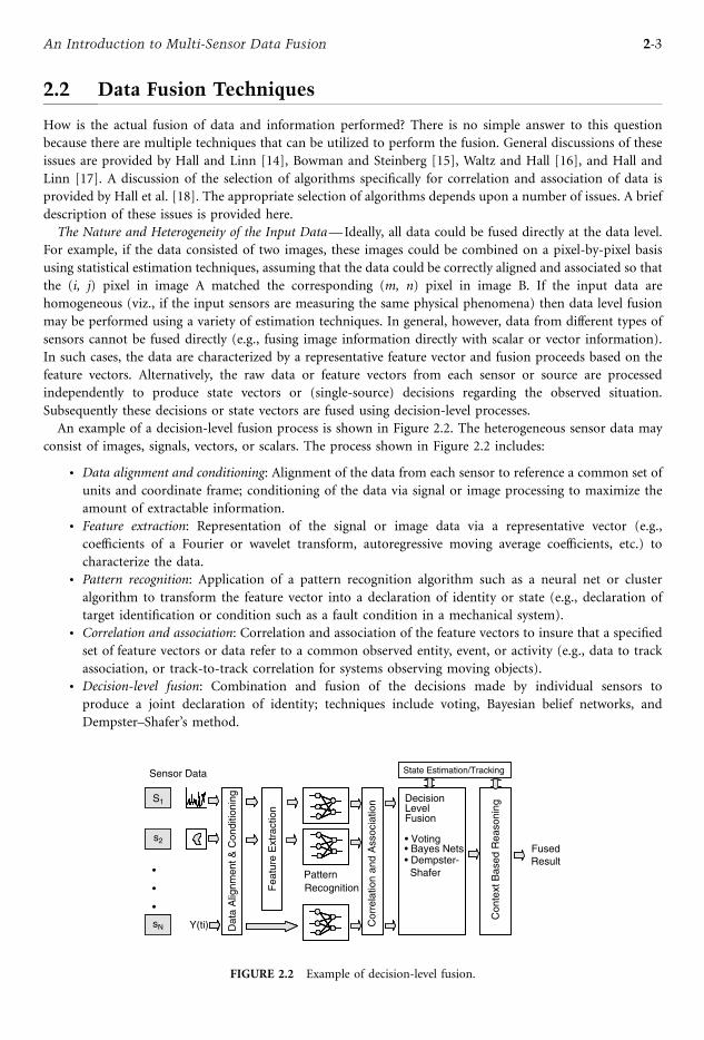
2.2 Data Fusion Techniques
How is the actual fusion of data and information performed? There is no simple answer to this question
because there are multiple techniques that can be utilized to perform the fusion. General discussions of these
issues are provided by Hall and Linn [14], Bowman and Steinberg [15], Waltz and Hall [16], and Hall and
Linn [17]. A discussion of the selection of algorithms specifically for correlation and association of data is
provided by Hall et al. [18]. The appropriate selection of algorithms depends upon a number of issues. A brief
description of these issues is provided here.
The Nature and Heterogeneity of the Input Data—Ideally, all data could be fused directly at the data level.
For example, if the data consisted of two images, these images could be combined on a pixel-by-pixel basis
using statistical estimation techniques, assuming that the data could be correctly aligned and associated so that
the (i, j) pixel in image A matched the corresponding (m, n) pixel in image B. If the input data are
homogeneous (viz., if the input sensors are measuring the same physical phenomena) then data level fusion
may be performed using a variety of estimation techniques. In general, however, data from different types of
sensors cannot be fused directly (e.g., fusing image information directly with scalar or vector information).
In such cases, the data are characterized by a representative feature vector and fusion proceeds based on the
feature vectors. Alternatively, the raw data or feature vectors from each sensor or source are processed
independently to produce state vectors or (single-source) decisions regarding the observed situation.
Subsequently these decisions or state vectors are fused using decision-level processes.
An example of a decision-level fusion process is shown in Figure 2.2. The heterogeneous sensor data may
consist of images, signals, vectors, or scalars. The process shown in Figure 2.2 includes:
. Data alignment and conditioning: Alignment of the data from each sensor to reference a common set of
units and coordinate frame; conditioning of the data via signal or image processing to maximize the
amount of extractable information.. Feature extraction: Representation of the signal or image data via a representative vector (e.g.,
coefficients of a Fourier or wavelet transform, autoregressive moving average coefficients, etc.) to
characterize the data.. Pattern recognition: Application of a pattern recognition algorithm such as a neural net or cluster
algorithm to transform the feature vector into a declaration of identity or state (e.g., declaration of
target identification or condition such as a fault condition in a mechanical system).. Correlation and association: Correlation and association of the feature vectors to insure that a specified
set of feature vectors or data refer to a common observed entity, event, or activity (e.g., data to track
association, or track-to-track correlation for systems observing moving objects).. Decision-level fusion: Combination and fusion of the decisions made by individual sensors to
produce a joint declaration of identity; techniques include voting, Bayesian belief networks, and
Dempster–Shafer’s method.
S1
s 2
s N
S1
s 2
s N
S1
s2
sN
Sensor Data
Dat
aA
lignm
ent&
Con
ditio
ning
Fea
ture
Ext
ract
ion
PatternRecognition
State Estimation/Tracking
FusedResult
Con
text
Bas
edR
easo
ning
Cor
rela
tion
and
Ass
ocia
tion
Y(ti)
DecisionLevelFusion
• Voting• Bayes Nets• Dempster-
Shafer
FIGURE 2.2 Example of decision-level fusion.
2-3An Introduction to Multi-Sensor Data Fusion

TABLE 2.1 Techniques for Data Fusion
Function Description Example Techniques References
Data alignment Alignment of data from
different sensors to be
processed in a common
frame of space and time
* Coordinate transformations* Adjustment of units
[53]
[2]
[58]
[60]
Data/object
correlation
and association
Grouping data together to
insure that the data all refer
to a common entity, target,
event or activity
* Gating methods [55]* Multiple hypothesis
association; probabilistic
data association* Figures of merit* Nearest neighbor
[56]
[57]
[59]
[61]
[62]
Signal
conditioning
Techniques to process input
signal or image data to improve
subsequent fusion processing
* A very wide variety of signal
and image processing
methods exist; see the general
references provided
[63]
Feature
extraction
Characterization of signal and
image data via vector
representations
* Time domain/time series
representations
[106]
[107]* Time-frequency representations* Higher order spectral methods [108]* Wavelet methods [96]
[97]
Pattern
recognition
Recognition of patterns in data;
transformation from input
feature vector to declaration
of target identity, classification
of phenomena, activity or
event detection
* Physical models [63]* Cluster algorithms [64]* Neural networks [65]* Syntactic models [66]* Hybrid reasoning models [67]
[68]
[69]
[70]
[71]
[72]
[73]
Decision-level
fusion
Fusion of reports or declarations
of target or entity identity; fusion
of reports for joint declarations
* Rule-based systems [74]* Bayes networks [75]* Fuzzy logic systems [76]* Intelligent agents [77]* Blackboard systems [78]* Case-based reasoning [79]
[80]
[81]
[82]
[83]
[84]
[85]
[86]
[87]
State estimation
and tracking
Estimation of the state vector or
system state based on observations
and/or feature vectors; tracking
the evolution of parameters in
time and/or space
* State estimators [55]* Kalman filters [56]* Particle trackers [88]* Multiple hypothesis
trackers (MHT)
[89]
* Probabalistic data
association (PDA)
[90]
* Interacting multiple
models (IMM)
[91]
[92]
[93]
[94]
[95]
(Continued on next page)
2-4 Sensors, Nanoscience, Biomedical Engineering, and Instruments
. Estimation and tracking: Estimation of the state vector(s) in time to produce a target or feature vector
track; this allows prediction of the state of the system in time.. Context-based reasoning: Application of automated reasoning techniques to interpret the meaning of
the fused data (e.g., relationships among objects or targets, understanding the meaning of the
environment, etc.).
Note that this process flow is intended to be conceptual only. An actual implemented data fusion systemwould
combine and interleave some of the functions identified in the figure. For example, in Figure 2.2 the state
estimation function (viz., the utilization of an estimator such as a Kalman filter to estimate a state vector such as
the position and velocity of an observed target) is shown as being separate from the identity level decision fusion.
However, in a real fusion system, these functions might be combined via a multiple hypothesis tracking
algorithm. A summary of types of algorithms corresponding to the functions in Figure 2.2 are listed in Table 2.2.
The A Priori Knowledge about the Input Data and Estimation Processes – Different techniques require
different levels of knowledge about the nature of the input data and the observation process. For example,
probabilistic methods such as Bayes method require a priori knowledge about the accuracy of the sensing
process and the state estimation process. For target tracking, extensive probability models may be developed
related to the sensing process, nature of the observed targets, the target tracking estimation process, etc. [55].
If such information is not available, then less restrictive models such as least-squares methods or voting
techniques must be used. The selection of fusion algorithms must consider what can realistically be assumed or
known about the observation and estimation process.
The Overall Data Fusion Architecture – A third factor that affects the selection of algorithms is the physical
and logical architecture for the sensing/fusion system. Are the sensors and processors geographically
distributed? Can all data be sent to a centralized processor for fusion or is processing performed at individual
sensor nodes? Methods for allocating data fusion processes among system processing nodes and corresponding
selection of algorithms are discussed by Hall and Llinas [5]. The rapid evolution of smart sensors and wireless
communications systems [104] has increasingly led to distributed data fusion systems. Architectures for
distributed fusion systems are described by Liggins and Chong [103].
2.3 Applications of Data Fusion
There are numerous evolving applications of data fusion. A summary of several emerging areas is provided in
Table 2.2 and summarized below.
TABLE 2.1 (Continued)
Function Description Example Techniques References
Context-based
reasoning
Automated reasoning about the
context of the observed situation;
interpretation of the meaning of
activities, events, association
among tracked or identified
entities; understanding the
relationship of the observed
entities with respect to the
environment
* Knowledge-based systems [74]* Rule-based expert systems [75]* Fuzzy logic logical templating [76]* Neural networks [77]* Case-based reasoning [78]* Intelligent agent systems [79]
[80]
[83]
[84]
[98]
Process control
and resource
allocation
Allocate use of sensor or
observing resources; refinement
of the on-going fusion process
for improved inferences
* Multi-objective optimization [99]* Utility theory [100]* E-commerce auction methods [101]* Genetic algorithms [102]
[103]
Source: Adapted from D.L. Hall and J. Llinas, ‘‘An introduction to multisensor data fusion,’’ Proc. IEEE, vol. 85, no. 1, pp. 6–23,1997.
2-5An Introduction to Multi-Sensor Data Fusion

. Condition-Based Monitoring (CBM) of Complex Systems – The ability to instrument complex systems
such as aircraft mechanical systems using MEMS sensors provides the opportunity to create intelligent
health monitoring systems [19–21]. Such systems monitor the current health and state of a mechanical
system, identify precursors to failure conditions, classify and identify faults, and seek to predict time to
failure (under assumed operating demands). The motivation for CBM is driven by a combination of
concern for safety and for reduced maintenance costs. In military systems, for example, the total
ownership cost of a large-scale platform such as a ship, submarine, or airplane is driven by maintenance
costs. Over 40% of the life-cycle cost of such a system involves maintenance. Currently, maintenance is
performed using a time-based or use-based approach (viz., perform maintenance after so many hours
or miles of operation). Time- or use-based maintenance is unduly expensive since it is performed in
anticipation of potential failures. Perfectly good equipment may have preventive maintenance
performed on it. In addition to the cost of unnecessary maintenance, the very act of maintenance can
induce errors or problems, even when such maintenance is performed correctly. Thus, there is extensive
research related to application of fusion for determining the condition and time to failure for complex
mechanical systems [34–37].. Environmental Monitoring – Environmental monitoring is another potential application for multi-sensor
data fusion [32, 33]. The need to determine the condition of crops, water supplies, soil conditions, weather
conditions, and the potential for environmental contamination (due to natural or man-made disasters)
requires multiple types of sensors such as infrared, visible, temperature, humidity, and other types of
sensors. Data fusion provides the opportunity to improve knowledge and assessment of an area of interest
by combining these diverse types of data. Observing platforms may include satellites, airborne
reconnaissance, ground-based sensors, and human observers. Advances in environmental monitoring
include the use of hyper-spectral image sensors and unattended ground based sensors. Exciting research is
ongoing to utilize insects and plants as sensing devices. An example of a data fusion system for
environmental monitoring is shown in Figure 2.3.
TABLE 2.2 Summary of Emerging Applications
Application Focus Types of Inferences References
Condition-based
monitoring of
complex systems
Monitoring the health
and status of complex
mechanical systems;
e.g., helicopters
* Status of machinery [7]* Identification of evidence
of impending failure
conditions
[19]
[20]
[21]* Classification of fault
conditions* Prediction of time to failure
Environmental
monitoring
Observing and understanding
the physical environment,
e.g. monitoring weather,
crop phenomena
* Condition of environmental
phenomena (e.g., weather, terrain)
[32]
[33]* Condition of crops* Spread of dust, flooding, etc.
Medical
applications
Utilization of multiple sensors
and sources to determine the
health and condition of
human or animal bodies
* Identification of medical
conditions
[22]
[23]* Medical diagnosis [24]* Characterization of tumors or
biological phenomena
[31]
Nondestructive
evaluation (NDE)
Determining the condition
and constituency of materials
or products without using
destructive testing
* Product testing [25]* Evaluation of material condition
(e.g., search for flaws or weaknesses)
[26]
[27]
[29]
Military
applications
Utilization of multiple sensors
and sources for improved
understanding of a
battle-space environment
* Automatic target recognition* Target tracking* Threat identification* Situation assessment
[28]
[2]
[3]
[9]
[30]
2-6 Sensors, Nanoscience, Biomedical Engineering, and Instruments
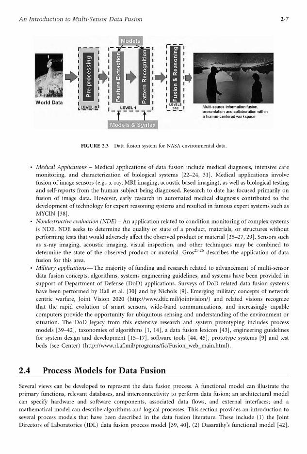
. Medical Applications – Medical applications of data fusion include medical diagnosis, intensive care
monitoring, and characterization of biological systems [22–24, 31]. Medical applications involve
fusion of image sensors (e.g., x-ray, MRI imaging, acoustic based imaging), as well as biological testing
and self-reports from the human subject being diagnosed. Research to date has focused primarily on
fusion of image data. However, early research in automated medical diagnosis contributed to the
development of technology for expert reasoning systems and resulted in famous expert systems such as
MYCIN [38].. Nondestructive evaluation (NDE) – An application related to condition monitoring of complex systems
is NDE. NDE seeks to determine the quality or state of a product, materials, or structures without
performing tests that would adversely affect the observed product or material [25–27, 29]. Sensors such
as x-ray imaging, acoustic imaging, visual inspection, and other techniques may be combined to
determine the state of the observed product or material. Gros25,26 describes the application of data
fusion for this area.. Military applications—The majority of funding and research related to advancement of multi-sensor
data fusion concepts, algorithms, systems engineering guidelines, and systems have been provided in
support of Department of Defense (DoD) applications. Surveys of DoD related data fusion systems
have been performed by Hall et al. [30] and by Nichols [9]. Emerging military concepts of network
centric warfare, Joint Vision 2020 (http://www.dtic.mil/jointvision/) and related visions recognize
that the rapid evolution of smart sensors, wide-band communications, and increasingly capable
computers provide the opportunity for ubiquitous sensing and understanding of the environment or
situation. The DoD legacy from this extensive research and system prototyping includes process
models [39–42], taxonomies of algorithms [1, 14], a data fusion lexicon [43], engineering guidelines
for system design and development [15–17], software tools [44, 45], prototype systems [9] and test
beds (see Center) (http://www.rl.af.mil/programs/fic/Fusion_web_main.html).
2.4 Process Models for Data Fusion
Several views can be developed to represent the data fusion process. A functional model can illustrate the
primary functions, relevant databases, and interconnectivity to perform data fusion; an architectural model
can specify hardware and software components, associated data flows, and external interfaces; and a
mathematical model can describe algorithms and logical processes. This section provides an introduction to
several process models that have been described in the data fusion literature. These include (1) the Joint
Directors of Laboratories (JDL) data fusion process model [39, 40], (2) Dasarathy’s functional model [42],
FIGURE 2.3 Data fusion system for NASA environmental data.
2-7An Introduction to Multi-Sensor Data Fusion
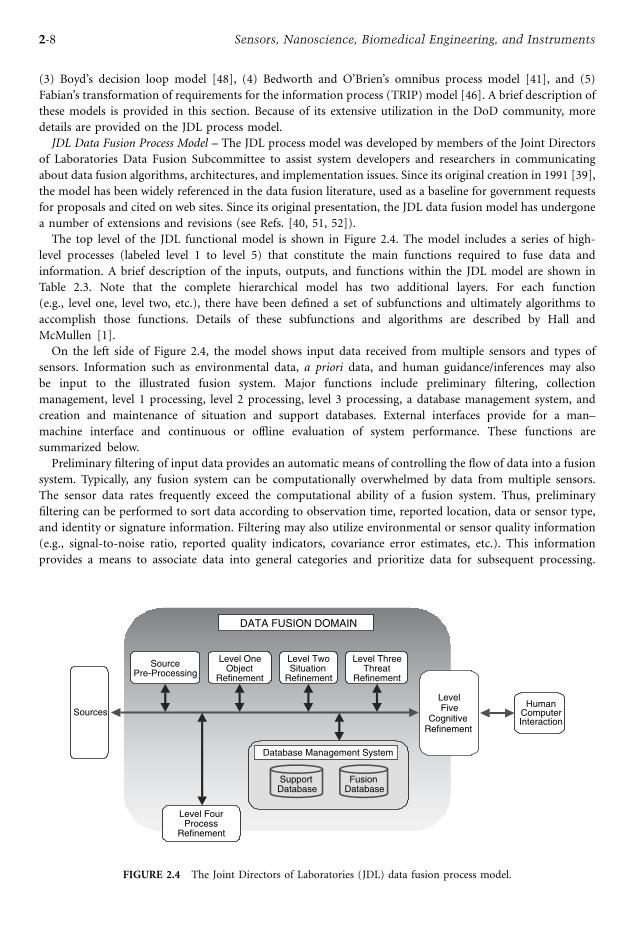
(3) Boyd’s decision loop model [48], (4) Bedworth and O’Brien’s omnibus process model [41], and (5)
Fabian’s transformation of requirements for the information process (TRIP) model [46]. A brief description of
these models is provided in this section. Because of its extensive utilization in the DoD community, more
details are provided on the JDL process model.
JDL Data Fusion Process Model – The JDL process model was developed by members of the Joint Directors
of Laboratories Data Fusion Subcommittee to assist system developers and researchers in communicating
about data fusion algorithms, architectures, and implementation issues. Since its original creation in 1991 [39],
the model has been widely referenced in the data fusion literature, used as a baseline for government requests
for proposals and cited on web sites. Since its original presentation, the JDL data fusion model has undergone
a number of extensions and revisions (see Refs. [40, 51, 52]).
The top level of the JDL functional model is shown in Figure 2.4. The model includes a series of high-
level processes (labeled level 1 to level 5) that constitute the main functions required to fuse data and
information. A brief description of the inputs, outputs, and functions within the JDL model are shown in
Table 2.3. Note that the complete hierarchical model has two additional layers. For each function
(e.g., level one, level two, etc.), there have been defined a set of subfunctions and ultimately algorithms to
accomplish those functions. Details of these subfunctions and algorithms are described by Hall and
McMullen [1].
On the left side of Figure 2.4, the model shows input data received from multiple sensors and types of
sensors. Information such as environmental data, a priori data, and human guidance/inferences may also
be input to the illustrated fusion system. Major functions include preliminary filtering, collection
management, level 1 processing, level 2 processing, level 3 processing, a database management system, and
creation and maintenance of situation and support databases. External interfaces provide for a man–
machine interface and continuous or offline evaluation of system performance. These functions are
summarized below.
Preliminary filtering of input data provides an automatic means of controlling the flow of data into a fusion
system. Typically, any fusion system can be computationally overwhelmed by data from multiple sensors.
The sensor data rates frequently exceed the computational ability of a fusion system. Thus, preliminary
filtering can be performed to sort data according to observation time, reported location, data or sensor type,
and identity or signature information. Filtering may also utilize environmental or sensor quality information
(e.g., signal-to-noise ratio, reported quality indicators, covariance error estimates, etc.). This information
provides a means to associate data into general categories and prioritize data for subsequent processing.
HumanComputerInteraction
Sources
DATA FUSION DOMAIN
Level FourProcess
Refinement
SourcePre-Processing
Level OneObject
Refinement
Level TwoSituation
Refinement
Database Management System
SupportDatabase
FusionDatabase
Level ThreeThreat
Refinement
LevelFive
CognitiveRefinement
FIGURE 2.4 The Joint Directors of Laboratories (JDL) data fusion process model.
2-8 Sensors, Nanoscience, Biomedical Engineering, and Instruments
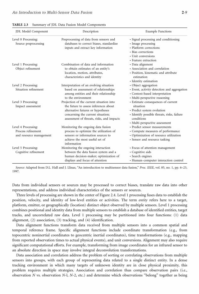
Data from individual sensors or sources may be processed to correct biases, translate raw data into other
representations, and address individual characteristics of the sensors or sources.
Three levels of processing are shown in the center of Figure 2.4. Level 1 processing fuses data to establish the
position, velocity, and identity of low-level entities or activities. The term entity refers here to a target,
platform, emitter, or geographically (location) distinct object observed by multiple sensors. Level 1 processing
combines positional and identity data from multiple sensors to establish a database of identified entities, target
tracks, and uncorrelated raw data. Level 1 processing may be partitioned into four functions: (1) data
alignment, (2) association, (3) tracking, and (4) identification.
Data alignment functions transform data received from multiple sensors into a common spatial and
temporal reference frame. Specific alignment functions include coordinate transformation (e.g., from
topocentric noninertial coordinates to geocentric inertial coordinates), time transformations (e.g., mapping
from reported observation times to actual physical events), and unit conversions. Alignment may also require
significant computational efforts. For example, transforming from image coordinates for an infrared sensor to
an absolute direction in space may involve integral deconvolution transformations.
Data association and correlation address the problem of sorting or correlating observations from multiple
sensors into groups, with each group of representing data related to a single distinct entity. In a dense
tracking environment in which many targets of unknown identity are in close physical proximity, this
problem requires multiple strategies. Association and correlation thus compare observation pairs (i.e.,
observation N vs. observation N-l, N-2, etc.) and determine which observations ‘‘belong’’ together as being
TABLE 2.3 Summary of JDL Data Fusion Model Components
JDL Model Component Description Example Functions
Level 0 Processing:
Source preprocessing
Preprocessing of data from sensors and
databases to correct biases, standardize
inputs and extract key information
* Signal processing and conditioning* Image processing* Platform corrections* Bias corrections* Unit conversions* Feature extraction
Level 1 Processing:
Object refinement
Combination of data and information
to obtain estimates of an entity’s
location, motion, attributes,
characteristics and identity
* Data alignment* Association and correlation* Position, kinematic and attribute
estimation* Identity estimation
Level 2 Processing:
Situation refinement
Interpretation of an evolving situation
based on assessment of relationships
among entities and their relationship
to the environment
* Object aggregation* Event, activity detection and aggregation* Context-based interpretation* Multi-perspective reasoning
Level 3 Processing:
Impact assessment
Projection of the current situation into
the future to assess inferences about
alternative futures or hypotheses
concerning the current situation;
assessment of threats, risks, and impacts
* Estimate consequences of current
situation* Predict system evolution* Identify possible threats, risks, failure
conditions* Multi-perspective assessment
Level 4 Processing:
Process refinement
and resource management
Monitoring the ongoing data fusion
process to optimize the utilization of
sensors or information sources to
achieve the most useful set of
information
* Predict sensor measurements* Compute measures of performance* Optimization of resource utilization* Sensor and resource tasking
Level 5 Processing:
Cognitive refinement
Monitoring the ongoing interaction
between the data fusion system and a
human decision-maker; optimization of
displays and focus of attention
* Focus of attention management* Cognitive aids* Search engines* Human–computer interaction control
Source: Adapted from D.L. Hall and J. Llinas, ‘‘An introduction to multisensor data fusion,’’ Proc. IEEE, vol. 85, no. 1, pp. 6–23,1997.
2-9An Introduction to Multi-Sensor Data Fusion
from the same entity, object, event, or activity. Association and correlation also seek to determine which, if
any, new observations belong to an observation or group of observations already contained in the fusion
database. Clearly, this problem scales as N2, where N is the current number of observations or tracks in the
database. The term association is generally used to describe the process of measuring the ‘‘closeness’’
between observation pairs (or observations to tracks), while the term correlation is used to describe the
decision process of actually assigning observations to observations, observations to tracks, or tracks to
tracks.
Tracking refers to a process in which multiple observations of positional data are combined to determine an
estimate of the target/entities position and velocity. A common tracking problem involves direction finding, in
which multiple angular observations (e.g., lines of bearing) are combined to estimate the location of a
nonmoving target. Another common tracking problem involves the use of observations from radar to establish
the track of an aircraft. Tracking algorithms begin with an a priori estimate of an object’s location and velocity
(viz., either an initial estimate based on a minimum data set, or an a priori track established in the database)
and update the estimated position to the time of a new observation. The new observation is utilized to refine
the position estimate to account for the new data. Tracking algorithms are closely coupled to association
strategies, particularly in a dense tracking environment.
Identification completes the category of level 1 processing functions. Identification methods seek to
combine identity information, analogous to the estimation of position utilizing positional data. Identity
fusion combines data related to identity (i.e., either actual declarations of identity from sensors, or parametric
data that can be related to identity). Identity fusion techniques include cluster methods, adaptive neural
networks, templating methods, and Dempster–Shaffer and Bayesian inference methods.
Level 2 processing or situation assessment seeks a higher level of inference above level 1 processing. Thus,
for example, while level 1 processing results in an order of battle (e.g., location and identity of low level
entities such as emitters or platforms), level 2 processing aims to assess the meaning or patterns in the order
of battle data. To obtain an assessment of the situation, the data are assessed with respect to the environment,
relationships among entities, and patterns in time and space.
Level 3 processing (for military or intelligence fusion systems) performs threat assessment. The purpose of
threat assessment is to determine the meaning of the fused data from an adversarial view. Threat assessment
functions include determination of lethality of friendly and enemy forces, assessment of friendly (‘‘blue force’’)
and enemy (‘‘red force’’) compositions, estimate of danger, evaluation of indications and warnings of
impending events, targeting calculations, and weapon assessment calculations. Level 3 processing is an
inferential process to assess the enemy’s threat or future implication of the current situation.
In order to manage the ongoing data fusion process, a level 4 meta-process is often used. This is a process
that monitors the data collection and the fusion processing to optimize the collection and processing of data
to achieve accurate and useful inferences. The level 4 process is deliberately shown as being partly inside and
partly outside the data fusion process. The reason is that actions could be taken by the level 4 process
(e.g., use active sensors) that could impede an operational mission. Hence, level 4 processing must be
cognizant of mission needs and constraints. Within level 4 processing, the collections management function
manages or controls the data collection assets (sensors) available to a fusion system. Specific functions involve
determining the availability of sensors, tasking sensors to perform collections, prioritization of tasking, and
monitoring sensor health/status in a feedback loop. Sensor tasking, in particular, requires predicting the future
location of dynamic objects to be observed, computing the pointing angles for a sensor (viz., from the
predicted position of an object and location of the sensor it computes the directions, ranges, etc., required for
a sensor to point to a target), computing the controls for sensor pointing scheduling the sensor’s observations,
and optimizing the use of sensor resources (e.g., power requirements or movement from one target to
another). For a large sensor network, the collection management function can be extremely challenging.
Ideally, the collection management function should work in concert with other data fusion functions to
optimize the rate and accuracy of inferences output from the fusion system.
Finally, a fifth level of processing was proposed by Hall et al. [51] to recognize the importance of
addressing human in the loop decision processes. Level 5 processing involves functions such as human–
computer interaction, cognitive aides to reduce human biases, adaptation of information needs and system
2-10 Sensors, Nanoscience, Biomedical Engineering, and Instruments

control to individual user preferences and constraints, automated interpretation of data using multiple
human sensory mechanisms, and tools such as search engines. The purpose of the level 5 processing is to
help adapt the fusion system to the human-in-the-loop decision maker and to improve the effectiveness of
the fusion system for supporting a human operation such as crisis management or situation assessment.
Functions in a fusion system include database management, man–machine interface, and evaluation
functions. These functions may actually comprise a major portion of a fusion system.
Dasarathy’s Functional Model – Dasarathy [42] defined a categorization of data fusion functions based on
types of data, the information to be processed, and the types of information that result from the fusion
process. The input is partitioned among data (e.g., signals and images), features (feature vectors), or objects
(decision-level reports related to objects or identity declarations). The output data are partitioned in the same
way as data, features, or object information. Dasarathy describes processes for each of the nine combinations
of input/output characteristics (e.g., data input/data output, data input/features output, features input/object
information output, etc.). For each of these categories, Dasarathy’s model identifies types of algorithms which
are suitable for processing. Steinberg and Bowman [47] have developed an expanded view of this model and
have linked Dasarathy’s view to the JDL model levels.
Boyd’s Decision Loop Model – Col. John Boyd [48, 49] articulated the concept of an Observe, Orient, Decide,
and Act (OODA) loop for effective tactical command and control in a military situation. This common sense
but effective method for addressing dynamic decision-making situations has been applied to a variety of
domains including driver’s education, library science, and crisis management. The process entails systematic
mindfulness of four key steps:
. Observe – Gather information via human senses, sensing devices, and other information sources
. Orient – Perform a situation assessment to understand the observed data and information
. Decide – Consider the likelihood of alternate hypotheses and their consequences and select the
best alternative. Act – Perform the indicated actions including possible collection of additional data
Development of tools and techniques to automate or support these steps is one way to view information
fusion processing.
Bedworth and O’Brien’s Omnibus Model – Bedworth and O’Brien [41] reviewed a number of different data
fusion models and synthesized an omnibus model. The model is similar to Boyd’s decision loop model but
incorporates or maps levels of the JDL model to the decision loop as well as linking aspects of the systems
engineering waterfall model and general components of the intelligence (disseminate, evaluate, collate, and
collect) cycle. The Omnibus model associates key fusion functions to the OODA loop functions. For example,
pattern matching and feature extraction are linked to the orient OODA step. Similarly, signal processing and
sensing are linked to the observe OODA step.
Transformation of Requirements to Information Processing (TRIP) Model – A team led by William Fabien
[50], under contract to the Defense Advanced Research Projects Agency (DARPA), developed a model called
the TRIP model. This model seeks to define the transformation of information needs by a tactical commander
to the specific tasking of sensors and information sources. Kessler and Fabien [50] suggest that the model has
four basic purposes:
. To describe the process for formulating collection tasks based on information needs or requirements
. To understand the interaction and relationships between collection management and the situation
estimation process. To understand how the human-in-the-loop decision maker interacts with the ongoing collection
management process and the situation assessment/fusion process. To understand how internal and external drivers affect the intelligence, surveillance, and reconnaissance
(ISR) process
The TRIP model is quite detailed and has been used to develop a hierarchy of functions, processes, and
the inputs and outputs. The TRIP model is focused primarily on tactical military applications, but could be
useful for other applications due to its level of detail.
2-11An Introduction to Multi-Sensor Data Fusion

2.5 Limitations of Data Fusion Systems
It is only fair in this introduction to data fusion to identify some limitations of data fusion systems. Hall and
Steinberg [105] have discussed these limitations and identified a number of issues or ‘‘dirty secrets’’ in data
fusion systems. These are summarized below. A summary of the state of the art in data fusion, based on the
JDL model, is provided in Table 2.4.
TABLE 2.4 Summary of the State of the Art in Data Fusion
JDL Process Current Practices Limitations and Challenges
Level 1: Object
refinement
* Sensor preprocessing using standard signal
and image processing methods
* Dense target environments* Rapidly maneuvering targets
* Explicit separation of correlation and
estimation problem
* Complex signal propagation* Co-dependent sensor observations
* Multiple target tracking using multiple
hypothesis tracking (MHT).
* Background clutter* Context-based reasoning
* Use of ad hoc maneuver models * Integration of identity and kinematic data* Object identification dominated by feature
based methods
* Lack of available training data (for target
identification)* Pattern recognition using neural networks * No true fusion of image and non-image
data (at the data level)* Emerging guidelines for selection of
correlation algorithms
Level 2: Situation
refinement
* Numerous prototype systems * Limited operational systems* Dominance of rule-based knowledge-based
systems (KBS)
* No experience in scaling up prototypes to
operational systems* Variations include blackboard systems, logical
templating, and case-based reasoning* Emerging use of fuzzy-logic and
agent-based systems
* Very limited cognitive models* Perfunctory test and evaluation against
toy problems* No proven technique for knowledge
engineering
Level 3: Threat
refinement
* Same as Level 2 processing * Same as Level 2* Limited advisory status * Difficulty to quantify intent* Limited deployment experience * Models require established enemy doctrine* Dominated by ad hoc methods * Difficult to model rapidly evolving situations* Doctrine-specific, fragile implementations* Very limited ability to predict the evolution
of phenomena (e.g., failure phenomena)* Emerging use of hybrid reasoning involving
implicit and explicit information
Level 4: Process
refinement
* Robust methods for single-sensor systems * Difficult to incorporate mission constraints* Formulations based on operations research* Limited context-based reasoning* Focus on measures of performance (MOP) versus
measures of effectiveness (MOE)
* Scaling problem when many sensors
(10N) and adaptive systems* Difficult to optimally use
noncommensurate sensors* Emerging use of auction-based methods from
e-commerce applications
* Very difficult to link human information
needs to sensor control* Emerging use of agents as proxies for
bidding for resources
Human–computer
interface (HCI)
* HCI dominated by the technology of the week* Focus on ergonomic versus cognitive-based design* Numerous graphics-based displays and systems
* Very little research has been performed
to understand how human analysts
process data and make accurate inferences* Advanced, 3D full immersion HCI available
and haptic interfaces* Initial experiments with multi-modal
sensory interactions
* Creative HCI is needed to adapt to
individual users and to provide mitigation
of known cognitive biases and illusions
* Initial experiments with agent-based
cognitive aids
2-12 Sensors, Nanoscience, Biomedical Engineering, and Instruments

. There is no substitute for a good sensor: No amount of data fusion can substitute for a single accurate
sensor that measures the phenomena that you want to observe. While a combination of sensors may
provide robust system operation, these sensors will not necessarily observe the feature of interest. For
example, in a mechanical system, conditions such as operating speed, vibration levels, and lubrication
pressure may provide valuable information about a system’s operation. However, these do not provide
direct evidence of the system operating temperature. In this example, the introduction of an
appropriate sensor such as a thermometer of a thermo-couple would obtain the desired information
about the state of the system.. Downstream processing cannot make up for errors (or failures) in upstream processing: Data fusion
processing cannot correct for errors in processing (or lack of preprocessing) of individual sensor
processing. For example, failure to identify and extract the correct features from a signal cannot be
corrected by a sophisticated pattern recognition scheme. Hence, attention must be paid to every step in
the data fusion processing flow.. Sensor fusion can result in poor performance if incorrect information about sensor performance is used:
A common problem in data fusion is to characterize the sensor performance in an ad hoc or convenient
(but incorrect) way. Failure to accurately model sensor performance will result in a corruption of the
fused results, because the sensor weights (or effects of the data from individual sensors) will be
incorrect. This is especially difficult for sensors in complex observing environments (e.g., involving a
difficult signal transmission media, complex interference environment, etc.).. There is no such thing as a magic or golden data fusion algorithm: Despite claims to the contrary, there is
no perfect algorithm that is optimal under all conditions. Real applications may not meet the
underlying assumptions required by data fusion algorithms. (e.g., available prior probabilities or
statistically independent sources). Thus, algorithm selection requires knowledge about the
characteristics of the observing environment, sensor performance, the processing environment, and
the fundamental information requirements of the candidate algorithms.. There will never be enough training data: In general, there will never be sufficient training data for
pattern recognition algorithms applications such as automatic target recognition. Hence, hybrid
methods must be used (e.g., model-based methods, syntactical representations, or combinations of
methods).. It is difficult to quantify the value of a data fusion system: A challenge in data fusion systems is to quantify
the utility of the system at a mission level. While measures of performance can be obtained for sensors
or processing algorithms, measures of mission effectiveness are difficult to define. How does the
application of data fusion algorithms assist in discovering how well a system (e.g., machine, factory,
weapon system) will perform in an operational environment?. Fusion is not a static process: Finally, the data fusion process in not static, but rather an iterative dynamic
process that seeks to continually refine the estimates about an observed situation or threat
environment. The level 4 process seeks to optimize the ongoing fusion process.
These factors should be kept in mind in studying and applying methods in data fusion.
2.6 Summary
The advent of smart micro- and nano-scale sensors, wideband communications, and rapidly evolving
microprocessors enable the creation of multi-sensor data fusion systems for use in a wide variety of applications
such as monitoring complex systems, environmental monitoring, medical diagnosis, or military applications.
Limitations of observation capability and communications are giving away to the limitations of the ability to
ingest or fuse the heterogeneous data. This chapter provided a brief introduction to the concepts of data fusion.
Development of information fusion systems for increased understanding of the observed environment or
situation involves understanding and utilization of a diverse set of algorithms and techniques. These range from
signal and image processing to pattern recognition, statistical estimation, optimization techniques, and
2-13An Introduction to Multi-Sensor Data Fusion

automated reasoning. The enormous legacy provided by DoD developments has laid the groundwork for a new
generation of intelligent sensing and fusion systems.
References
1. D. Hall and S.A. McMullen, Mathematical Techniques in Multisensor Data Fusion, 2nd ed., Norwood,
MA: Artech House, 2004.
2. E. Waltz and Llinas, J., Multisensor Data Fusion, Norwood, MA: Artech House, 1990.
3. E. Waltz, ‘‘C3I: A tutorial,’’ in Command, Control, Communications Intelligence (C3I), Palo Alto, CA: EW
Communications, 1986, pp. 217–226.
4. L.A. Klein, Sensor and Data Fusion Concepts and Applications, New York: SPIE Optical Engineering
Texts, 1993.
5. D.L. Hall and J. Llinas, Eds., Handbook of Multisensor Data Fusion, The Electrical and Applied Signal
Processing Series, Boca Raton, FL: CRC Press, 2001.
6. D.L. Hall and J. Llinas, ‘‘An introduction to multisensor data fusion,’’ Proc. IEEE, vol. 85, no. 1, pp. 6–
23, 1997.
7. C.S. Byington and A.K. Garga, ‘‘Data fusion for developing predictive diagnostics for electromechanical
systems,’’ in Handbook of Multisensor Data Fusion, D.L. Hall and J. Llinas, Eds., The Electrical and
Applied Signal Processing Series, Boca Raton, FL: CRC Press, 2001, pp 23-1–23-30.
8. J.D. Williams, ‘‘Use of biometrics and biomedical imaging in support of battlefield diagnostics,’’ in
Fusion ’98: First Int. Conf. Multi-Source, Multi-Sens. Info. Fusion, Las Vegas, NV, 1998.
9. M.L. Nichols, ‘‘A survey of multisensor data fusion systems,’’ in Handbook of Multisensor Data Fusion,
D.L. Hall and J. Llinas, Eds., The Electrical and Applied Signal Processing Series, Boca Raton, FL: CRC
Press, FL, 2001, pp. 22-1–22-7.
10. D.G. Goodenough, P. Bhogal, D. Charlebois, S. Matwin, and O. Niemann, ‘‘Intelligent data fusion for
remote sensing,’’ Proc. Intl. Geosci. and Remote Sensing Symp., IGARSS, vol. 3, pp. 2157–2160, 1995.
11. N. Malud, An Introduction to Microelectromechanical Systems, Norwood, MA: Artech House, 1999.
12. D.C. Swanson, Signal Processing for Intelligent Sensor Systems, New York: Marcel Dekker, 2000.
13. M.A. Trenas, J.C. Rutledge, and N.A. Whitmal, ‘‘Wavelet-based noise reduction and compression for
hearing aids,’’ Proc. IEEE 21st Int. Conf. IEEE Eng. Med. Biol. Soc., October 1999.
14. D. Hall and R. Linn, ‘‘A taxonomy of multisensor data fusion algorithms,’’ Proc. 1990 Joint Serv. Data
Fusion Symp., Johns Hopkins University Applied Research Laboratory, Laurel, MD. vol. 1, 1990,
pp. 593–610.
15. C. Bowman and A. Steinberg, ‘‘A systems engineering approach for implementing data fusion systems,’’
in Handbook of Multisensor Data Fusion, D.L. Hall and J. Llinas, Eds., The Electrical and Applied Signal
Processing Series, Boca Raton, FL: CRC Press, 2001, pp. 16-1–16-38.
16. E. Waltz and D. Hall, ‘‘Requirements derivation for data fusion systems,’’ in Handbook of Multisensor
Data Fusion, D.L. Hall and J. Llinas, Eds., The Electrical and Applied Signal Processing Series, Boca
Raton, FL: CRC Press, 2001, pp. 15-1–15-8.
17. D.L. Hall and R. Linn, ‘‘Algorithm selection for data fusion systems,’’ Proc. 1987 Tri-Service Data Fusion
Symp., Laurel, MD: Applied Physics Laboratory, Johns Hopkins University, vol. 1, pp. 100–110, 1987.
18. D.L. Hall, J. Llinas, B. Neuenfeldt, L. McConnell, D. Bohney, C. Bowman, L. Lochocki, and P. Applegate,
‘‘Studies and analyses within project correlation: An in-depth assessment of correlation problems and
solution techniques,’’ Proc. Ninth Natl Symp. Sens. Fusion, Monterey, CA: Naval Postgraduate School,
12–14 March 1996, pp. 171–188.
19. C.S. Byington and A.K. Garga, ‘‘Platform level reasoning for an SH-60B helicopter using intelligent
agents,’’ Proc. 54th Soc. Mach. Fail. Prev. Technol., Virginia Beach, VA, 2000.
20. D.L. Hall, R.J. Hansen, and S.K. Kurtz, ‘‘A new approach to the challenge of machinery prognostics,’’
J. Eng. Gas Turb. Power, Trans. Am. Soc. Mech. Eng. (ASME), April 1995, pp. 320–325.
21. D.L. Hall, R.J. Hansen, and D.C. Lang, ‘‘The negative information problem in mechanical diagnostics,’’
Trans. ASME 119, 370–377, 1997.
2-14 Sensors, Nanoscience, Biomedical Engineering, and Instruments

22. H. Alto et al., ‘‘Image processing: radiological and clinical information fusion in breast cancer detection,’’
Proc. SPIE Conf. Sens. Fusion: Architect., Algorithms Appl. IV, Orlando, FL, 3–5 April, 2002, pp. 134–181.
23. M. Akay and A. Marsh, Eds., Information Technologies in Medicine, Vol. 1, Medical Simulation and
Education, New York: Wiley-IEEE Computer Society, 2001.
24. J. Webster, Ed., Minimally Invasive Medical Technology, New York: Institute of Physics Publisher,
2001.
25. X.E. Gros, Ed., NDT Data Fusion, New York: Arnold, 1997.
26. X.E. Gros, Ed., Applications of NDT Data Fusion, New York: Kluwer Academic, 2001.
27. F. Ansari, Ed., Condition Monitoring of Materials and Structures, American Society of Civil Engineering
Publishers, 2000.
28. R. Antony, Principles of Data Fusion Automation, Norwood, MA: Artech House, 1995.
29. G.W. Nickerson and D.L. Hall, ‘‘NDT: The blurring distinction between NDT and onboard
diagnostics,’’ in Proc. 34th Annu. Br. Conf. NDT, London, U.K., June 1995.
30. D.L. Hall, R. Linn, and J. Llinas, ‘‘A survey of data fusion systems,’’ Proc. SPIE Conf. Data Struct. Target
Classif., April 1991, pp. 13–29.
31. J.M. Martin and D. Tobin, Principles and Practice of Intensive Care, New York: McGraw Hill, 1997.
32. J. Jahnke, Continuous Emission Monitoring, 2nd ed., New York: Wiley, 2000.
33. A. Camara and A.S. Da Camara, Environmental Systems: A Multidimensional Approach, Oxford: Oxford
University Press, 2002.
34. D. Hall, A. Garga, B. Grimes, S. Kumara, I. Petrick, and S. Purao, ‘‘Intelligent preparation of the
logistics battle space: The role of data fusion,’’ Proc. 2004 MSS Nal Symp. Sens. Data Fusion, Johns
Hopkins University Applied Physics Laboratory, June 8–10, 2004.
35. D. Hall, K. Schroyer, S.A. McMullen, and J.J. McMullen, ‘‘On the use of analog problems to address
level-2 and level-3 information fusion,’’ Proc. 2004 MSS Natl Symp. Sens. Data Fusion, Johns Hopkins
University Applied Physics Laboratory, June 8–10, 2004.
36. J. Erdley, Improved Fault Detection using Multisens. Data Fusion, M.S. thesis in Electrical Engineering,
The Pennsylvania State University, 1997.
37. D. Hall, ‘‘Intelligent monitoring of complex systems,’’ in Advances in Intelligent Systems for Defence,
L.C. Jain, N.S. Ichalkaranje, and G. Tonfoni, Eds., World Scientific Publishing Company, 2003.
38. B.G. Buchanon and E.H. Shortliffe, Rule-Based Expert Systems: The MYCIN Experts of the Heuristic
Programming Project, Reading, MA: Addison-Wesley, 1983.
39. O. Kessler, K. Askin, N. Beck, J. Lynch, F. White, D. Buede, D. Hall, and J. Llinas, Functional Description
of the Data Fusion Process, Technical report developed for the Data Fusion Development Strategy,
Office of Naval Technology, Warminster, PA, November, 1991.
40. A.N. Steinberg, C.L. Bowman, and F.E. White, ‘‘Revisions to the JDL data fusion process model,’’ in
Proc. SPIE AeroSense: Sens. Fusion: Architectures, Algorithms Appl. III, B. Dasarathy and F.L. Orlando,
Eds., vol. 3719, 1999, pp 430–441.
41. M. Bedworth and O’Brien, ‘‘The Omnibus model: A new model of data fusion?,’’ in Proc. 2nd Int. Conf.
Info. Fusion, Johns Hopkins University Applied Physics Laboratory, May 24–27, 1999 (see http://
www.inforfusion.org/fusion99/cdrom.htm).
42. B. Dasarathy, Decision Fusion, New York: IEEE Computer Society Press, 1994.
43. D. Hall, Lexicon of Multisensor Data Fusion Terms, State College, PA: Tech Reach, 1997.
44. S.A. Hall and R.S. Sherry, ‘‘A survey of COTS software for multisensor data fusion: What’s new since
Hall and Linn?,’’ Proc. 2002 MSS Natl Symp. Sens. Data Fusion, San Diego, CA, 2002.
45. D. Hall and G. Kasmala, ‘‘A visual programming toolkit for multisensor data fusion,’’ Proc. SPIE
Aerospace 1996 Symp.: Digitization of the Battlefield, R. Suresh and W. Langford, Eds., vol. 2764,
Orlando, FL, March 1996, pp 181–187.
46. O. Kessler and B. Fabian, ‘‘Estimation and ISR Process Integration,’’ Def. Adv. Res. Proj. Agency
(DARPA) Tech. Rep., Washington, DC, 2001.
47. A. Steinberg and C. Bowman, ‘‘Revisions to the JDL data fusion processing model,’’ in Handbook of
Multisensor Data Fusion, D. Hall and J. Llinas, Eds., Boca Raton, FL: CRC Press, 2001, Chapter 2.
2-15An Introduction to Multi-Sensor Data Fusion

48. Boyd, R. John, A Discourse on Winning and Losing, August 1987, Private Collections. Master copy in
Library at Marine Corps University, Quantico, VA.
49. G. Hammond, The Mind of War: John Boyd and American Security, Washington, DC: Smithsonian
Institution Press, May 2001.
50. O. Kessler and B. Fabian, Estimation and the ISR process integration, technical briefing prepared for the
Defense Advanced Research Projects Agency (DARPA), Washington, D.C., 2001.
51. M.J. Hall, S.A. Hall, and T. Tate, ‘‘Removing the HCI bottleneck: how the human computer interface
(HCI) affects the performance of data fusion systems,’’ Proc. 2000 MSS Natl Symp. Sens. Data Fusion,
San Diego, CA, June 2000, pp. 89–104.
52. A. Steinberg and C. Bowman, ‘‘Rethinking the JDL data fusion levels,’’ Proc. 2004 MSS Natl Symp. Sens.
Data Fusion, Johns Hopkins University Applied Research Laboratory, June 7–9, 2004.
53. R. Escobal, Methods of Orbit Determination, Melbourne, FL: Krieger, 1976.
54. E.L. Zavaleta and E.J. Smith, Goddard Trajectory Determination System User’s Guide, Silver Spring, MD:
Computer Sciences Corporation Technical Report, 1975.
55. S. Blackman, Multiple Target Tracking with Radar Applications, Norwood, MA: Artech House, 1986.
56. Y. Bar-Shalom and E. Tse, ‘‘Tracking in a cluttered environment with probabilistic data association,’’
Automatica, 2, 451–460, 1975.
57. T.E. Fortman, Y. Bar-Shaolom, and M. Scheffe, ‘‘Multi-target tracking using joint probabilistic data
association,’’ in Proc. 1980 IEEE Conf. Decis. Control, December 1980, pp. 807–812.
58. J.O. Cappellari, C.E. Velez, and A.J. Fuchs, Mathematical Theory of the Goddard Trajectory
Determination System, Technical Report, Greenbelt, MD: NASA Goddard Space Flight Center, 1976.
59. F.L. Wright, ‘‘The fusion of multi-sensor data,’’ Signal, 1980, pp 39–43.
60. N.D. Sanza, M.A. McClure, and J.R. Cloutier, ‘‘Spherical target state estimators,’’ Proc. Am. Control
Conf., Baltimore, MD, June 1994, pp. 1675–1679.
61. M. de Feo, A. Graziano, R. Miglioli, and A. Farina, ‘‘IMMJPDA vs MHT and Kalman filter with NN
correlation: Performance comparison,’’ IEE Proc. Radar, Sonar Navigation, 144, pp. 49–52, 1999.
62. D. Lerro and Y. Bar-Shalom, ‘‘Interacting multiple models tracking with target amplification feature,’’
IEEE Trans. Aerospace Electron. Syst., AES-29, 494–509, 1993.
63. K. Fukanaga, Introduction to Statistical Pattern Recognition, 2nd ed., New York: Academic Press, 1990.
64. M.S. Aldenderfer and R.K. Blashfield, Cluster Analysis, in the series: Quantitative Applications in the
Social Sciences, No. 07-044, London: Sage Press, 1984.
65. R. Dubes and A. Jain, ‘‘Clustering algorithms in exploratory data analysis,’’ Advances in Computers, vol.
19, 1980, pp. 113–228.
66. H. Skinner, ‘‘Dimensions and clusters: A hybrid approach to classification,’’ App. Psycholog. Meas., 3,
327–341, 1979.
67. A.J. Cole and A. Wishart, ‘‘An improved algorithm for the Jardine-Sibson method of generating
clusters,’’ Comput. J., 13, 156–163, 1970.
68. R.P. Lippman, ‘‘An introduction to computing neural networks,’’ IEEE ASSP Mag., 3–4, 4–22, 1987.
69. B. Widrow and R. Winter, ‘‘Neural nets for adaptive filtering and adaptive pattern recognition,’’ IEEE
Comput., 21–3, 24–40, 1988.
70. D. Mush and B. Horne, ‘‘Progress in supervised neural networks: What’s new since Lippman?,’’
IEEE Signal Process. Mag., 8–39, January, 1993.
71. D. Touretzky, Advances in Neural Information Processing Systems, 2nd ed., Palo Alto, CA: Morgan
Kauffman, 1990.
72. R.O. Duda and P.E. Hart, Pattern Classification and Scene Analysis, New York: Wiley, 1973.
73. D. Hall and A. Garga, ‘‘Hybrid reasoning techniques for automated fault classification,’’ Proc. 51st Meet.
Soc. Mach. Fail. Prev., April, 1997.
74. R. Kurzwil, The Age of Intelligent Machines, Cambridge, MA: MIT Press, 1990.
75. P. Jackson, Introduction to Expert Systems, 3rd ed., New York: Addison-Wesley, 1998.
76. R.A. Benfer, E.E. Brent, and L. Furbee, Expert Systems, vol. 77, London: Sage, 1991.
77. J.C. Giarranto, Expert Systems: Principles and Programming, Pacific Grove, CA: Brooks/Cole, 1998.
2-16 Sensors, Nanoscience, Biomedical Engineering, and Instruments

78. R.E. Neopolitan, Probabilistic Reasoning in Expert Systems: Theory and Algorithms, New York: Wiley,
1990.
79. S. Post and A.P. Sage, ‘‘An overview of automated reasoning,’’ IEEE Trans. Syst., Man Cybernet., 20,
202–224, 1990.
80. K.C. Ng and B. Abramson, ‘‘Uncertainty management in expert systems,’’ IEEE Expert, 1990, pp. 29–48.
81. L.A. Zadeh, ‘‘Fuzzy logic,’’ Computer, 83–92, 1988.
82. J. Llinas and R. Antony, ‘‘Blackboard concepts for data fusion and command and control applications,’’
Proc. Int. J. Pattern Recogn. Artif. Intel., 1992.
83. D.F. Noble, ‘‘Template-based data fusion for situation assessment,’’ in Proc. 1987 Tri-Service Data
Fusion Symp., Laurel, MD: Johns Hopkins University, Applied Physics Laboratory, 1987, pp. 226–236.
84. D.L. Hall and R.J. Linn, ‘‘Comments on the use of templating for multi-sensor data fusion,’’ Proc. 1989
Tri-Service Data Fusion Symp., Laurel, MD: Johns Hopkins University Applied Physics Laboratory,
1989, pp. 152–162.
85. F.V. Jensen, Bayesian Networks and Decision Graphs, New York: Springer, 2001.
86. M. Woodridge, Introduction to Multi-Agent Systems, New York: John Wiley and Sons, 2002.
87. J. Yen, J. Yin, T.R. Ioerger, M. Miller, D. Xu, and R.A. Volz, ‘‘CAST: Collaborating agents simulating
teamwork,’’ Proc. Int. Joint Conf. Artif. Intel. (IJCAI 2001), Seattle, WA, 2001, pp. 1135–1142.
88. H.W. Sorenson, ‘‘Least squares estimation: from Gauss to Kalman,’’ IEEE Spectrum, July 1970,
pp. 63–68.
89. A. Gelb, Applied Optimal Estimation, Cambridge, MA: MIT Press, 1974.
90. A.H. Sayed and T. Kailath, ‘‘A state-space approach to adaptive RLS filtering,’’ IEEE Signal Process.
Mag., 18–70, July 1994.
91. A. Poore, ‘‘Multi-dimensional assignment formulation of the data association problem arising from
multi-target and multi-sensor tracking,’’ Comput. Optimiz. Appl., 3, 27–57, 1994.
92. R.L. Streit and T.E. Luginbuhl, ‘‘A probabilistic multi-hypothesis tracking algorithm without
enumeration and pruning,’’ in Proc. 6th Joint Serv. Data Fusion Symp., Laurel, MD: Johns Hopkins
University Applied Research Laboratory, June 1993.
93. R.L. Streit, ‘‘Maximum likelihood method for probabilistic multi-hypothesis tracking,’’ SPIE Proc.,
2234-5, 394–406, 1994.
94. R. Mahler, ‘‘A unified foundation for data fusion,’’ Proc. 1994 Data Fusion Syst. Conf., Laurel, MD:
Johns Hopkins University Applied Physics Laboratory, June 1987.
95. I.R. Goodman, R.S. Mahler, and H.T. Nguyen, Mathematics of Data Fusion, New York: Kluwer
Academic, 1997.
96. Kittler, ‘‘Mathematical methods in feature selection in pattern recognition,’’ Int. J. Man-Mach. Stud., 7,
609–637, 1975.
97. C. Lee and D.A. Landgrebe, ‘‘Decision boundary feature extraction for nonparametric classification,’’
Trans. Syst. Man Cybernet., 23, 433–444, 1993.
98. M. Lenz, B. Bartsch-Spori, H. Burkhard, S. Wess, G. Goos, J. Hartmanis, and J. Van Leeuwan, Case-
Based Reasoning Technology: From Foundation to Application, New York: Springer-Verlag, 1998.
99. G.A. McIntyre, A Comprehensive Approach to Sensor Management and Scheduling, Ph.D. dissertation,
Department of Information Technology, George Mason University, 1998.
100. A.N. Steinberg, ‘‘Threat management systems for combat aircraft,’’ Proc. Tri-Serv. Data Fusion Symp.,
Laurel, MD: Johns Hopkins University, 1987, pp. 532–52.
101. P.L. Rothman and S.G. Bier, ‘‘Evaluation of sensor management systems,’’ Proc. 1991 Fusion Syst. Conf.,
Laurel, MD: Johns Hopkins University Applied Physics Laboratory, October 1991.
102. P.C. Fishburn, Nonlinear Preference and Utility Theory, Laurel, MD: Johns Hopkins University Press,
1988.
103. M.E. Liggins II and C.Y. Chong, ‘‘Distributed fusion architectures and algorithms for target tracking,’’
Proc. IEEE, vol. 85, no. 1, 1997.
104. C.Y. Chong and S.P. Kumar, ‘‘Sensor networks: evolution, opportunities, and challenges,’’ Proc. IEEE,
vol. 91, no. 8, 2003.
2-17An Introduction to Multi-Sensor Data Fusion

105. D. Hall and A. Steinberg, ‘‘Dirty secrets in multisensor data fusion,’’ in Handbook of Multisensor Data
Fusion, D.L. Hall and J. Llinas, Eds., The Electrical and Applied Signal Processing Series, Boca Raton,
FL: CRC Press, 2001.
106. A. Weigend and N.A. Gershenfeld, Time Series Prediction: Forecasting the Future and Understanding the
Past, Reading, MA: Addison Wesley, 1994.
107. L. Cohen, ‘‘Time frequency distribution – a review,’’ Proc. IEEE, 77, 941–981, 1989.
108. P.A. Delany and D.O. Walsh, ‘‘A bibliography of higher order spectra and cumulants,’’ IEEE Signal
Process. Mag., 61–74, July 1994.
2-18 Sensors, Nanoscience, Biomedical Engineering, and Instruments

3Magneto-optics
David YoungRockwell Semiconductor Systems
Yuan PuUniversity of California
3.1 Introduction ........................................................................ 3-1
3.2 Classification of Magneto-optic Effects .................................... 3-2Faraday Rotation or Magnetic Circular Birefringence *
Cotton–Mouton Effect or Magnetic Linear
Birefringence * Kerr Effects
3.3 Applications of Magneto-optic Effects ..................................... 3-5Optical Isolator and Circulator * MSW-Based Guided-Wave
Magneto-optic Bragg Cell * Magneto-optic Recording
3.1 Introduction
When a magnetic field H is applied to a magnetic medium (crystal), a change in the magnetization M within
the medium will occur as described by the constitution relation of the Maxwell equations M ¼ w$ ·H where w$
is the magnetic susceptibility tensor of the medium. The change in magnetization can in turn induce a
perturbation in the complex optical permittivity tensor e$. This phenomenon is called the magneto-optic
effect. Mathematically, the magneto-optic effect can be described by expanding the permittivity tensor as a
series in increasing powers of the magnetization (Torfeh et al., 1977) as follows:
e$ ¼ e0½eij ð3:1Þ
where
eijðMÞ ¼ erdij þ jf1eijkMk þ fijklMkMl
Here, j is the imaginary number. M1, M2, and M3 are the magnetization components along the principal
crystal axes X, Y, and Z, respectively. e0 is the permittivity of free space. er is the relative permittivity of themedium in the paramagnetic state (i.e., M ¼ 0), f1 is the first-order magneto-optic scalar factor, fijkl is the
second-order magneto-optic tensor factor, dij is the Kronecker delta, and eijk is the antisymmetric alternate
index of the third order. Here we have used Einstein notation of repeated indices and have assumed that the
medium is quasi-transparent so that e$ is a Hermitian tensor. Moreover, we have also invoked the Onsager
relation in thermo-dynamical statistics, i.e., eij(M) ¼ eji( M). The consequences of Hermiticity and Onsager
relation are that the real part of the permittivity tensor is an even function ofM whereas the imaginary part is
an odd function of M. For a cubic crystal, such as yttrium–iron–garnet (YIG), the tensor fijkl reduces to only
three independent terms. In terms of Voigt notation, they are f11, f12, and f44. In a principal coordinate system,
the tensor can be expressed as
fijkl ¼ f12dijdkl þ f44ðdildkj þ dikdljÞ þ Df dkldijdjk ð3:2Þ
where Df ¼ f11 f12 2f44:
3-1
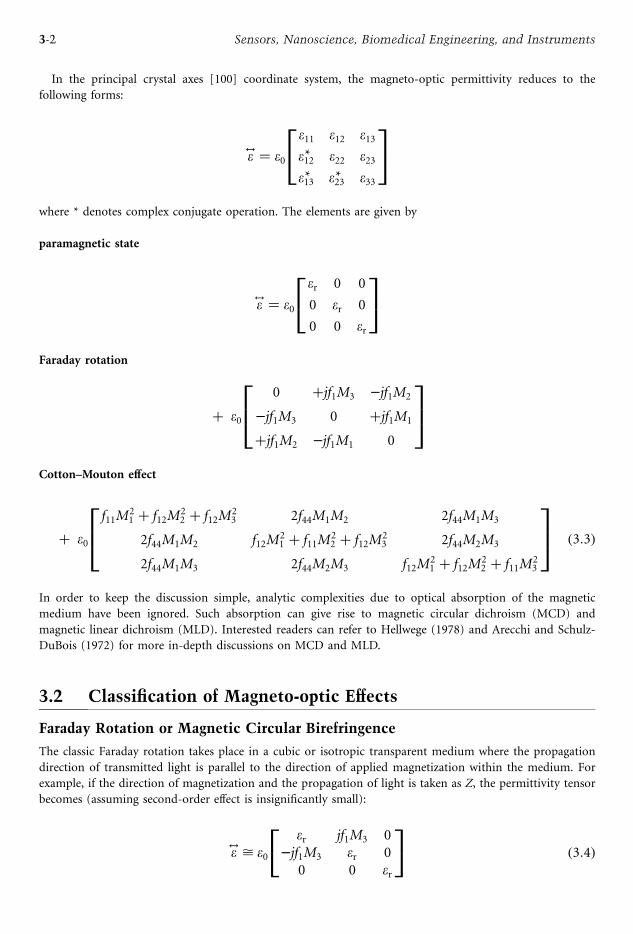
In the principal crystal axes [100] coordinate system, the magneto-optic permittivity reduces to the
following forms:
e$ ¼ e0
e11 e12 e13e12* e22 e23e13* e23* e33
264375
where * denotes complex conjugate operation. The elements are given by
paramagnetic state
e$ ¼ e0
er 0 0
0 er 0
0 0 er
264375
Faraday rotation
þ e0
0 þjf1M3 jf1M2
jf1M3 0 þjf1M1
þjf1M2 jf1M1 0
26643775
Cotton–Mouton effect
þ e0
f11M21 þ f12M
22 þ f12M
23 2f44M1M2 2f44M1M3
2f44M1M2 f12M21 þ f11M
22 þ f12M
23 2f44M2M3
2f44M1M3 2f44M2M3 f12M21 þ f12M
22 þ f11M
23
26643775 ð3:3Þ
In order to keep the discussion simple, analytic complexities due to optical absorption of the magnetic
medium have been ignored. Such absorption can give rise to magnetic circular dichroism (MCD) and
magnetic linear dichroism (MLD). Interested readers can refer to Hellwege (1978) and Arecchi and Schulz-
DuBois (1972) for more in-depth discussions on MCD and MLD.
3.2 Classification of Magneto-optic Effects
Faraday Rotation or Magnetic Circular Birefringence
The classic Faraday rotation takes place in a cubic or isotropic transparent medium where the propagation
direction of transmitted light is parallel to the direction of applied magnetization within the medium. For
example, if the direction of magnetization and the propagation of light is taken as Z, the permittivity tensor
becomes (assuming second-order effect is insignificantly small):
e$ > e0er jf1M3 0jf1M3 er 00 0 er
24 35 ð3:4Þ
3-2 Sensors, Nanoscience, Biomedical Engineering, and Instruments
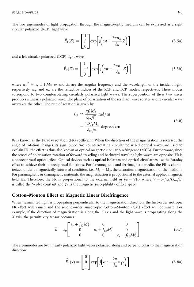
The two eigenmodes of light propagation through the magneto-optic medium can be expressed as a right
circular polarized (RCP) light wave:
E~1ðZÞ ¼1j0
24 35exp j ot2pnþl0
Z ð3:5aÞ
and a left circular polarized (LCP) light wave:
E~2ðZÞ ¼1j
0
24 35exp j ot2pnl0
Z ð3:5bÞ
where n^2 > er ^ f1M3; o and l0 are the angular frequency and the wavelength of the incident light,
respectively. nþ and n are the refractive indices of the RCP and LCP modes, respectively. These modes
correspond to two counterrotating circularly polarized light waves. The superposition of these two waves
produces a linearly polarized wave. The plane of polarization of the resultant wave rotates as one circular wave
overtakes the other. The rate of rotation is given by
yF >pf1M3
l0ffiffiffier
p rad=m
¼ 1:8f1M3
l0ffiffiffier
p degree=cm
ð3:6Þ
yF is known as the Faraday rotation (FR) coefficient. When the direction of the magnetization is reversed, the
angle of rotation changes its sign. Since two counterrotating circular polarized optical waves are used to
explain FR, the effect is thus also known as optical magnetic circular birefringence (MCB). Furthermore, since
the senses of polarization rotation of forward traveling and backward traveling light waves are opposite, FR is
a nonreciprocal optical effect. Optical devices such as optical isolators and optical circulators use the Faraday
effect to achieve their nonreciprocal functions. For ferromagnetic and ferrimagnetic media, the FR is charac-
terized under a magnetically saturated condition, i.e.,M3 ¼ MS, the saturation magnetization of the medium.
For paramagnetic or diamagnetic materials, the magnetization is proportional to the external applied magnetic
field H0. Therefore, the FR is proportional to the external field or yF ¼ VH0 where V ¼ w0f1p=ðl0 ffiffiffier
p Þis called the Verdet constant and w0 is the magnetic susceptibility of free space.
Cotton–Mouton Effect or Magnetic Linear Birefringence
When transmitted light is propagating perpendicular to the magnetization direction, the first-order isotropic
FR effect will vanish and the second-order anisotropic Cotton–Mouton (CM) effect will dominate. For
example, if the direction of magnetization is along the Z axis and the light wave is propagating along the
X axis, the permittivity tensor becomes
e$ ¼ e0er þ f12M
23 0 0
0 er þ f12M23 0
0 0 er þ f11M23
24 35 ð3:7Þ
The eigenmodes are two linearly polarized light waves polarized along and perpendicular to the magnetization
direction:
EejjðxÞ ¼ 001
24 35exp j ot2pl0nkx ð3:8aÞ
3-3Magneto-optics
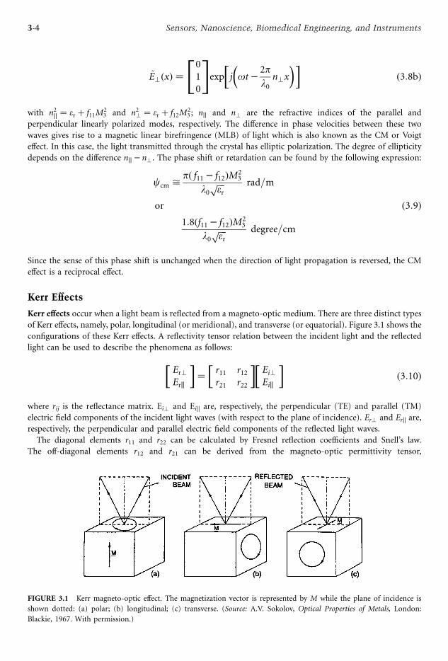
E~’ðxÞ ¼010
24 35exp j ot2pl0n’x ð3:8bÞ
with n2jj ¼ er þ f11M23 and n2’ ¼ er þ f12M
23 ; njj and n’ are the refractive indices of the parallel and
perpendicular linearly polarized modes, respectively. The difference in phase velocities between these two
waves gives rise to a magnetic linear birefringence (MLB) of light which is also known as the CM or Voigt
effect. In this case, the light transmitted through the crystal has elliptic polarization. The degree of ellipticity
depends on the difference njj n’. The phase shift or retardation can be found by the following expression:
ccm >pð f11 f12ÞM2
3
l0ffiffiffier
p rad=m
or
1:8ðf11 f12ÞM23
l0ffiffiffier
p degree=cm
ð3:9Þ
Since the sense of this phase shift is unchanged when the direction of light propagation is reversed, the CM
effect is a reciprocal effect.
Kerr Effects
Kerr effects occur when a light beam is reflected from a magneto-optic medium. There are three distinct types
of Kerr effects, namely, polar, longitudinal (or meridional), and transverse (or equatorial). Figure 3.1 shows the
configurations of these Kerr effects. A reflectivity tensor relation between the incident light and the reflected
light can be used to describe the phenomena as follows:
Er’Erk
¼ r11 r12r21 r22
Ei’Eik
ð3:10Þ
where rij is the reflectance matrix. Ei’ and Ei|| are, respectively, the perpendicular (TE) and parallel (TM)
electric field components of the incident light waves (with respect to the plane of incidence). Er’ and Er|| are,
respectively, the perpendicular and parallel electric field components of the reflected light waves.
The diagonal elements r11 and r22 can be calculated by Fresnel reflection coefficients and Snell’s law.
The off-diagonal elements r12 and r21 can be derived from the magneto-optic permittivity tensor,
FIGURE 3.1 Kerr magneto-optic effect. The magnetization vector is represented by M while the plane of incidence is
shown dotted: (a) polar; (b) longitudinal; (c) transverse. (Source: A.V. Sokolov, Optical Properties of Metals, London:
Blackie, 1967. With permission.)
3-4 Sensors, Nanoscience, Biomedical Engineering, and Instruments
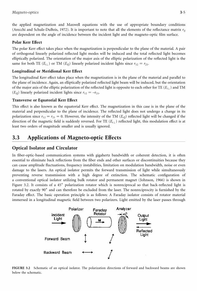
the applied magnetization and Maxwell equations with the use of appropriate boundary conditions
(Arecchi and Schulz-DuBois, 1972). It is important to note that all the elements of the reflectance matrix rijare dependent on the angle of incidence between the incident light and the magneto-optic film surface.
Polar Kerr Effect
The polar Kerr effect takes place when the magnetization is perpendicular to the plane of the material. A pair
of orthogonal linearly polarized reflected light modes will be induced and the total reflected light becomes
elliptically polarized. The orientation of the major axis of the elliptic polarization of the reflected light is the
same for both TE (Ei’) or TM (Ei||) linearly polarized incident lights since r12 ¼ r21.
Longitudinal or Meridional Kerr Effect
The longitudinal Kerr effect takes place when the magnetization is in the plane of the material and parallel to
the plane of incidence. Again, an elliptically polarized reflected light beam will be induced, but the orientation
of the major axis of the elliptic polarization of the reflected light is opposite to each other for TE (Ei’) and TM
(Ei||) linearly polarized incident lights since r12 ¼ –r21.
Transverse or Equatorial Kerr Effect
This effect is also known as the equatorial Kerr effect. The magnetization in this case is in the plane of the
material and perpendicular to the plane of incidence. The reflected light does not undergo a change in its
polarization since r12 ¼ r21 ¼ 0. However, the intensity of the TM (Er||) reflected light will be changed if the
direction of the magnetic field is suddenly reversed. For TE (Er’) reflected light, this modulation effect is at
least two orders of magnitude smaller and is usually ignored.
3.3 Applications of Magneto-optic Effects
Optical Isolator and Circulator
In fiber-optic-based communication systems with gigahertz bandwidth or coherent detection, it is often
essential to eliminate back reflections from the fiber ends and other surfaces or discontinuities because they
can cause amplitude fluctuations, frequency instabilities, limitation on modulation bandwidth, noise or even
damage to the lasers. An optical isolator permits the forward transmission of light while simultaneously
preventing reverse transmission with a high degree of extinction. The schematic configuration of
a conventional optical isolator utilizing bulk rotator and permanent magnet (Johnson, 1966) is shown in
Figure 3.2. It consists of a 45– polarization rotator which is nonreciprocal so that back-reflected light is
rotated by exactly 90– and can therefore be excluded from the laser. The nonreciprocity is furnished by the
Faraday effect. The basic operation principle is as follows: A Faraday isolator consists of rotator material
immersed in a longitudinal magnetic field between two polarizers. Light emitted by the laser passes through
FIGURE 3.2 Schematic of an optical isolator. The polarization directions of forward and backward beams are shown
below the schematic.
3-5Magneto-optics
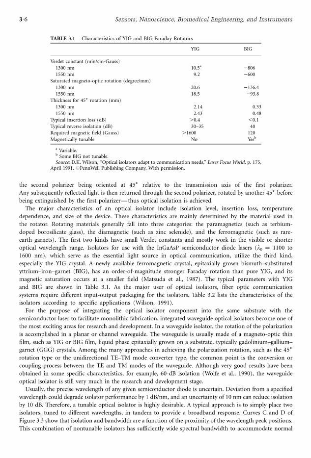
the second polarizer being oriented at 45– relative to the transmission axis of the first polarizer.
Any subsequently reflected light is then returned through the second polarizer, rotated by another 45– beforebeing extinguished by the first polarizer—thus optical isolation is achieved.
The major characteristics of an optical isolator include isolation level, insertion loss, temperature
dependence, and size of the device. These characteristics are mainly determined by the material used in
the rotator. Rotating materials generally fall into three categories: the paramagnetics (such as terbium-
doped borosilicate glass), the diamagnetic (such as zinc selenide), and the ferromagnetic (such as rare-
earth garnets). The first two kinds have small Verdet constants and mostly work in the visible or shorter
optical wavelength range. Isolators for use with the InGaAsP semiconductor diode lasers (l0 ¼ 1100 to
1600 nm), which serve as the essential light source in optical communication, utilize the third kind,
especially the YIG crystal. A newly available ferromagnetic crystal, epitaxially grown bismuth–substituted
yttrium–iron–garnet (BIG), has an order-of-magnitude stronger Faraday rotation than pure YIG, and its
magnetic saturation occurs at a smaller field (Matsuda et al., 1987). The typical parameters with YIG
and BIG are shown in Table 3.1. As the major user of optical isolators, fiber optic communication
systems require different input-output packaging for the isolators. Table 3.2 lists the characteristics of the
isolators according to specific applications (Wilson, 1991).
For the purpose of integrating the optical isolator component into the same substrate with the
semiconductor laser to facilitate monolithic fabrication, integrated waveguide optical isolators become one of
the most exciting areas for research and development. In a waveguide isolator, the rotation of the polarization
is accomplished in a planar or channel waveguide. The waveguide is usually made of a magneto-optic thin
film, such as YIG or BIG film, liquid phase epitaxially grown on a substrate, typically gadolinium–gallium–
garnet (GGG) crystals. Among the many approaches in achieving the polarization rotation, such as the 45–
rotation type or the unidirectional TE–TM mode converter type, the common point is the conversion or
coupling process between the TE and TM modes of the waveguide. Although very good results have been
obtained in some specific characteristics, for example, 60-dB isolation (Wolfe et al., 1990), the waveguide
optical isolator is still very much in the research and development stage.
Usually, the precise wavelength of any given semiconductor diode is uncertain. Deviation from a specified
wavelength could degrade isolator performance by 1 dB/nm, and an uncertainty of 10 nm can reduce isolation
by 10 dB. Therefore, a tunable optical isolator is highly desirable. A typical approach is to simply place two
isolators, tuned to different wavelengths, in tandem to provide a broadband response. Curves C and D of
Figure 3.3 show that isolation and bandwidth are a function of the proximity of the wavelength peak positions.
This combination of nontunable isolators has sufficiently wide spectral bandwidth to accommodate normal
TABLE 3.1 Characteristics of YIG and BIG Faraday Rotators
YIG BIG
Verdet constant (min/cm-Gauss)
1300 nm 10.5a 806
1550 nm 9.2 600
Saturated magneto-optic rotation (degree/mm)
1300 nm 20.6 136.4
1550 nm 18.5 93.8
Thickness for 45– rotation (mm)1300 nm 2.14 0.33
1550 nm 2.43 0.48
Typical insertion loss (dB) .0.4 ,0.1
Typical reverse isolation (dB) 30–35 40
Required magnetic field (Gauss) .1600 120
Magnetically tunable No Yesb
a Variable.b Some BIG not tunable.Source: D.K. Wilson, ‘‘Optical isolators adapt to communication needs,’’ Laser Focus World, p. 175,
April 1991. #PennWell Publishing Company. With permission.
3-6 Sensors, Nanoscience, Biomedical Engineering, and Instruments
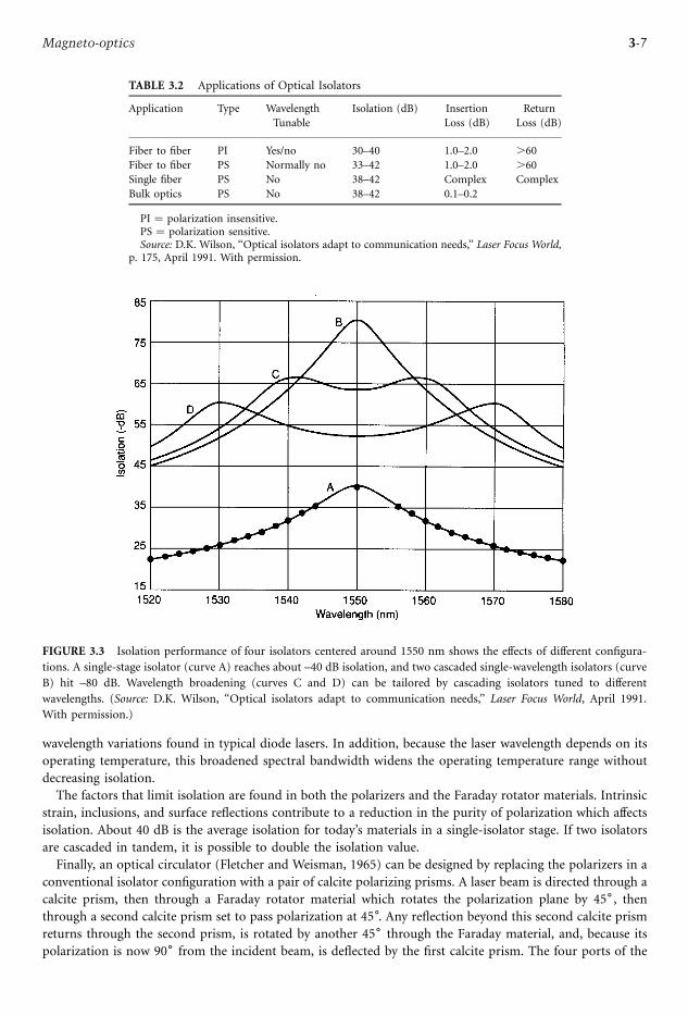
wavelength variations found in typical diode lasers. In addition, because the laser wavelength depends on its
operating temperature, this broadened spectral bandwidth widens the operating temperature range without
decreasing isolation.
The factors that limit isolation are found in both the polarizers and the Faraday rotator materials. Intrinsic
strain, inclusions, and surface reflections contribute to a reduction in the purity of polarization which affects
isolation. About 40 dB is the average isolation for today’s materials in a single-isolator stage. If two isolators
are cascaded in tandem, it is possible to double the isolation value.
Finally, an optical circulator (Fletcher and Weisman, 1965) can be designed by replacing the polarizers in a
conventional isolator configuration with a pair of calcite polarizing prisms. A laser beam is directed through a
calcite prism, then through a Faraday rotator material which rotates the polarization plane by 45–, thenthrough a second calcite prism set to pass polarization at 45–. Any reflection beyond this second calcite prismreturns through the second prism, is rotated by another 45– through the Faraday material, and, because itspolarization is now 90– from the incident beam, is deflected by the first calcite prism. The four ports of the
FIGURE 3.3 Isolation performance of four isolators centered around 1550 nm shows the effects of different configura-
tions. A single-stage isolator (curve A) reaches about –40 dB isolation, and two cascaded single-wavelength isolators (curve
B) hit –80 dB. Wavelength broadening (curves C and D) can be tailored by cascading isolators tuned to different
wavelengths. (Source: D.K. Wilson, ‘‘Optical isolators adapt to communication needs,’’ Laser Focus World, April 1991.
With permission.)
TABLE 3.2 Applications of Optical Isolators
Application Type Wavelength
Tunable
Isolation (dB) Insertion
Loss (dB)
Return
Loss (dB)
Fiber to fiber PI Yes/no 30–40 1.0–2.0 .60
Fiber to fiber PS Normally no 33–42 1.0–2.0 .60
Single fiber PS No 38–42 Complex Complex
Bulk optics PS No 38–42 0.1–0.2
PI ¼ polarization insensitive.PS ¼ polarization sensitive.Source: D.K. Wilson, ‘‘Optical isolators adapt to communication needs,’’ Laser Focus World,
p. 175, April 1991. With permission.
3-7Magneto-optics
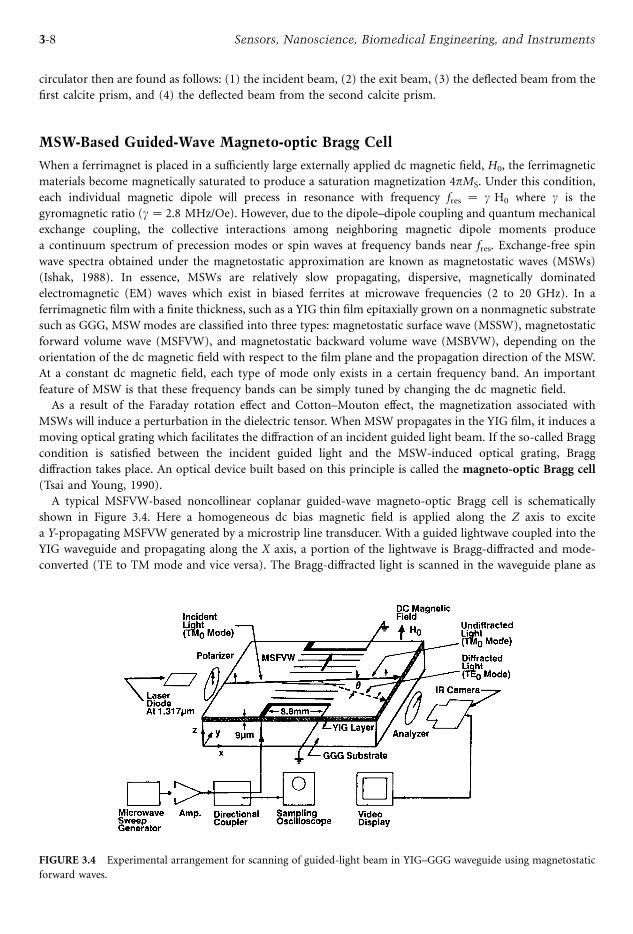
circulator then are found as follows: (1) the incident beam, (2) the exit beam, (3) the deflected beam from the
first calcite prism, and (4) the deflected beam from the second calcite prism.
MSW-Based Guided-Wave Magneto-optic Bragg Cell
When a ferrimagnet is placed in a sufficiently large externally applied dc magnetic field, H0, the ferrimagnetic
materials become magnetically saturated to produce a saturation magnetization 4pMS. Under this condition,
each individual magnetic dipole will precess in resonance with frequency fres ¼ g H0 where g is the
gyromagnetic ratio (g ¼ 2.8 MHz/Oe). However, due to the dipole–dipole coupling and quantum mechanical
exchange coupling, the collective interactions among neighboring magnetic dipole moments produce
a continuum spectrum of precession modes or spin waves at frequency bands near fres. Exchange-free spin
wave spectra obtained under the magnetostatic approximation are known as magnetostatic waves (MSWs)
(Ishak, 1988). In essence, MSWs are relatively slow propagating, dispersive, magnetically dominated
electromagnetic (EM) waves which exist in biased ferrites at microwave frequencies (2 to 20 GHz). In a
ferrimagnetic film with a finite thickness, such as a YIG thin film epitaxially grown on a nonmagnetic substrate
such as GGG, MSWmodes are classified into three types: magnetostatic surface wave (MSSW), magnetostatic
forward volume wave (MSFVW), and magnetostatic backward volume wave (MSBVW), depending on the
orientation of the dc magnetic field with respect to the film plane and the propagation direction of the MSW.
At a constant dc magnetic field, each type of mode only exists in a certain frequency band. An important
feature of MSW is that these frequency bands can be simply tuned by changing the dc magnetic field.
As a result of the Faraday rotation effect and Cotton–Mouton effect, the magnetization associated with
MSWs will induce a perturbation in the dielectric tensor. When MSW propagates in the YIG film, it induces a
moving optical grating which facilitates the diffraction of an incident guided light beam. If the so-called Bragg
condition is satisfied between the incident guided light and the MSW-induced optical grating, Bragg
diffraction takes place. An optical device built based on this principle is called the magneto-optic Bragg cell
(Tsai and Young, 1990).
A typical MSFVW-based noncollinear coplanar guided-wave magneto-optic Bragg cell is schematically
shown in Figure 3.4. Here a homogeneous dc bias magnetic field is applied along the Z axis to excite
a Y-propagating MSFVW generated by a microstrip line transducer. With a guided lightwave coupled into the
YIG waveguide and propagating along the X axis, a portion of the lightwave is Bragg-diffracted and mode-
converted (TE to TM mode and vice versa). The Bragg-diffracted light is scanned in the waveguide plane as
FIGURE 3.4 Experimental arrangement for scanning of guided-light beam in YIG–GGG waveguide using magnetostatic
forward waves.
3-8 Sensors, Nanoscience, Biomedical Engineering, and Instruments
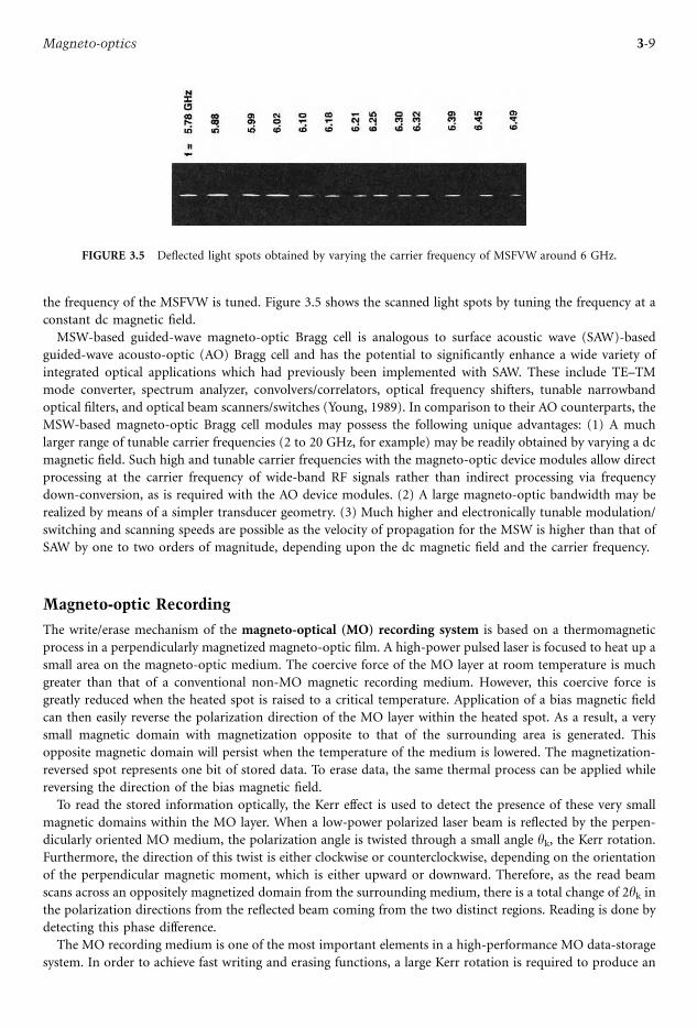
the frequency of the MSFVW is tuned. Figure 3.5 shows the scanned light spots by tuning the frequency at a
constant dc magnetic field.
MSW-based guided-wave magneto-optic Bragg cell is analogous to surface acoustic wave (SAW)-based
guided-wave acousto-optic (AO) Bragg cell and has the potential to significantly enhance a wide variety of
integrated optical applications which had previously been implemented with SAW. These include TE–TM
mode converter, spectrum analyzer, convolvers/correlators, optical frequency shifters, tunable narrowband
optical filters, and optical beam scanners/switches (Young, 1989). In comparison to their AO counterparts, the
MSW-based magneto-optic Bragg cell modules may possess the following unique advantages: (1) A much
larger range of tunable carrier frequencies (2 to 20 GHz, for example) may be readily obtained by varying a dc
magnetic field. Such high and tunable carrier frequencies with the magneto-optic device modules allow direct
processing at the carrier frequency of wide-band RF signals rather than indirect processing via frequency
down-conversion, as is required with the AO device modules. (2) A large magneto-optic bandwidth may be
realized by means of a simpler transducer geometry. (3) Much higher and electronically tunable modulation/
switching and scanning speeds are possible as the velocity of propagation for the MSW is higher than that of
SAW by one to two orders of magnitude, depending upon the dc magnetic field and the carrier frequency.
Magneto-optic Recording
The write/erase mechanism of the magneto-optical (MO) recording system is based on a thermomagnetic
process in a perpendicularly magnetized magneto-optic film. A high-power pulsed laser is focused to heat up a
small area on the magneto-optic medium. The coercive force of the MO layer at room temperature is much
greater than that of a conventional non-MO magnetic recording medium. However, this coercive force is
greatly reduced when the heated spot is raised to a critical temperature. Application of a bias magnetic field
can then easily reverse the polarization direction of the MO layer within the heated spot. As a result, a very
small magnetic domain with magnetization opposite to that of the surrounding area is generated. This
opposite magnetic domain will persist when the temperature of the medium is lowered. The magnetization-
reversed spot represents one bit of stored data. To erase data, the same thermal process can be applied while
reversing the direction of the bias magnetic field.
To read the stored information optically, the Kerr effect is used to detect the presence of these very small
magnetic domains within the MO layer. When a low-power polarized laser beam is reflected by the perpen-
dicularly oriented MO medium, the polarization angle is twisted through a small angle yk, the Kerr rotation.Furthermore, the direction of this twist is either clockwise or counterclockwise, depending on the orientation
of the perpendicular magnetic moment, which is either upward or downward. Therefore, as the read beam
scans across an oppositely magnetized domain from the surrounding medium, there is a total change of 2yk inthe polarization directions from the reflected beam coming from the two distinct regions. Reading is done by
detecting this phase difference.
The MO recording medium is one of the most important elements in a high-performance MO data-storage
system. In order to achieve fast writing and erasing functions, a large Kerr rotation is required to produce an
FIGURE 3.5 Deflected light spots obtained by varying the carrier frequency of MSFVW around 6 GHz.
3-9Magneto-optics
acceptable carrier-to-noise (C/N) ratio. In general, a high-speed MO layer has a read signal with a poor C/N
ratio, while a good read-performance MO layer is slow in write/erase sensitivity.
Defining Terms
Cotton–Mouton effect: Second-order anisotropic reciprocal magneto-optic effect which causes a linearly
polarized incident light to transmit through as an elliptically polarized output light wave when the
propagation direction of the incident light is perpendicular to the direction of the applied
magnetization of the magneto-optic medium. It is also known as magnetic linear birefringence (MLB).
Faraday rotation: First-order isotropic nonreciprocal magneto-optic effect which causes the polarization
direction of a linearly polarized transmitted light to rotate when the propagation direction of the
incident light wave is parallel to the direction of the applied magnetization of the magneto-optic
medium. It is also known as magnetic circular birefringence (MCB).
Kerr effects: Reflected light from a magneto-optic medium can be described by the optical Kerr effects.
There are three types of Kerr effects: polar, longitudinal, and transverse, depending on the directions of
the magnetization with respect to the plane of incidence and the reflecting film surface.
Magneto-optic Bragg cell: A magnetically tunable microwave signal processing device which uses optical
Bragg diffraction of light from a moving magneto-optic grating generated by the propagation of
magnetostatic waves within the magnetic medium.
Magneto-optic recording system: A read/write data recording system based on a thermomagnetic
process to write oppositely magnetized domains onto a magneto-optic medium by means of high-
power laser heating. Magneto-optic Kerr effect is then employed to read the data by using a low-power
laser as a probe beam to sense the presence of these domains.
Optical circulator: A four-port optical device that can be used to monitor or sample incident light (input
port) as well as reflected light (output port) with the two other unidirectional coupling ports.
Optical isolator: A unidirectional optical device which only permits the transmission of light in the
forward direction. Any reflected light from the output port is blocked by the device from returning to
the input port with a very high extinction ratio.
References
F.T. Arecchi and E.O. Schulz-DuBois, Laser Handbook, D4, Amsterdam: North-Holland, 1972, pp. 1009–1027.
P.C. Fletcher and D.L. Weisman, ‘‘Circulators for optical radar systems,’’ Appl. Opt., 4, pp. 867–873, 1965.
K.H. Hellwege, Landolt-Bornstein Numerical Data and Functional Relationships in Science and Technology,
New Series, vols. 4 and 12, New York: Springer, 1978.
W.S. Ishak, ‘‘Magnetostatic wave technology: a review,’’ in Proc. IEEE, vol. 76, pp. 171–187, 1988.
B. Johnson, ‘‘The Faraday effect at near infrared wavelength in rare-earth garnet,’’ Brit. J. Appl. Phys., 17, 1441,
1966.
K. Matsuda, H. Minemoto, O. Kamada, and S. Isbizuka, ‘‘Bi-substituted, rare-earth iron garnet composite film
with temperature independent Faraday rotation for optical isolators,’’ IEEE Trans. Mag., MAG-23, 3479,
1987.
M. Torfeh, L. Courtois, L. Smoczynski, H. Le Gall, and J.M. Desvignes, ‘‘Coupling and phase matching
coefficients in a magneto-optical TE-TM mode converter,’’ Physica, 89B, pp. 255–259, 1977.
C.S. Tsai and D. Young, ‘‘Magnetostatic-forward-volume-wave-based guided-waveless magneto-optic Bragg
cells and applications to communications and signal processing,’’ IEEE Trans. Microw. Theory Technol.,
vol. MTT-38, no. 5, pp. 560–30, 1990.
D.K. Wilson, ‘‘Optical isolators adapt to communication needs,’’ Laser Focus World, 175, 1991.
R. Wolfe et al., ‘‘Edge tuned ridge waveguide magneto-optic isolator,’’ Appl. Phys. Lett., 56, 426, 1990.
D. Young, ‘‘Guided wave magneto-optic Bragg cells using Yttrium Iron Garnet-Gadolinium Gallium Garnet
(YIG-GGG) thin film at microwave frequencies,’’ Ph.D. Dissertation, University of California, Irvine,
CA, 1989.
3-10 Sensors, Nanoscience, Biomedical Engineering, and Instruments

Further Information
Current publications on magneto-optics can be found in the following journals: Intermag Conference Proceed-
ings published by the IEEE and International Symposium Proceedings on Magneto-Optics.
For in-depth discussion on magnetic bubble devices, please see, for example, Magnetic-Bubble Memory
Technology by Hsu Chang, published by Marcel Dekker, 1978.
An excellent source of information on garnet materials can be found in Magnetic Garnet by Gerhard
Winkler, published by Friedr. Vieweg & Sohn, 1981.
Numerous excellent reviews on the subject of magneto-optics have been published over the years,
for example, J.F. Dillon, Jr., ‘‘Magneto-optics and its uses,’’ Journal of Magnetism and Magnetic Materials,
vol. 31–34, pp. 1–9, 1983; M.J. Freiser, ‘‘A survey of magneto-optic effects,’’ IEEE Transactions on Magnetics,
vol. MAG-4, pp. 152–161, 1968; G. A. Smolenskii, R.V. Pisarev, and I.G. Sinii, ‘‘Birefringence of light in
magnetically ordered crystals,’’ Sov. Phys. Usp., vol. 18, pp. 410–429, 1976; and A.M. Prokhorov, G.A.
Smolenskii, and A.N. Ageev, ‘‘Optical phenomena in thin-film magnetic waveguides and their technical
application,’’ Sov. Phys. Usp., vol. 27, pp. 339–362, 1984.
3-11Magneto-optics


4Materials andNanoscience
M. MeyyappanNASA Ames Research Center
John PeleskoUniversity of Delaware
Victor GiurgiutiuUniversity of South Carolina
Sergey Edward LyshevskiRochester Institute of Technology
Nelson TansuLehigh University
Ronald ArifLehigh University
Zhian JinLehigh University
4.1 Carbon Nanotubes .............................................................. 4-1Introduction * Structure and Properties * Growth * Nano-Electronics *
AFM Imaging Using CNT Probes * Sensors * Field Emission *
Summary
4.2 Modeling MEMS and NEMS ................................................ 4-9Micro- and Nano-Electromechanical Systems *
The Science of Scale * Modeling Approaches
4.3 Micromechatronics ............................................................. 4-20Introduction to Micromechatronics Systems * Synchronous
Micromachines * Fabrication Aspects * Electroactive and
Magnetoactive Materials * Induced-Strain Actuators *
Piezoelectric Wafer Active Sensors * Microcontrollers
Sensing, Actuation, and Process Control
4.4 Nanocomputers, Nano-Architectronics, and Nano-ICs ............. 4-42Introduction * Nano-Electronics and Nanocomputer Fundamentals *
Nanocomputer Architecture * Hierarchical Finite-State Machines
and Their Use in Hardware and Software Design *
Reconfigurable Nanocomputers * Mathematical Models for
Nanocomputers * Nanocompensator Synthesis and Design
Aspects
4.5 Semiconductor Nano-Electronics and Nano-Optoelectronics .... 4-68Introduction to Semiconductor Nanotechnology * Fundamental
Physics of Semiconductor Nanotechnology—Quantum Physics *
Semiconductor Nano-Electronics—Resonant Tunneling Diode *
Semiconductor Nano-Electronics—Single Electron Transistors *
Semiconductor Nano-Optoelectronics * Future: Quantum Effects
and Semiconductor Nanotechnology
4.1 Carbon Nanotubes
M. Meyyappan
Introduction
Carbon nanotubes (CNTs) were discovered in 1991 [1] by Sumio Iijima of the NEC Corporation. Since then,
research activities exploring their structure, properties, and applications have exploded across the world. Carbon
nanotubes exhibit unique electronic properties and extraordinary mechanical properties, and, hence, have
received attention in nano-electronics, sensors, actuators, field emission devices, high strength composites and a
host of other applications. A detailed discussion on properties, growth, characterization, and application
development can be found in a recent textbook [2]. Here, a brief overview of these subject matters is presented.
4-1
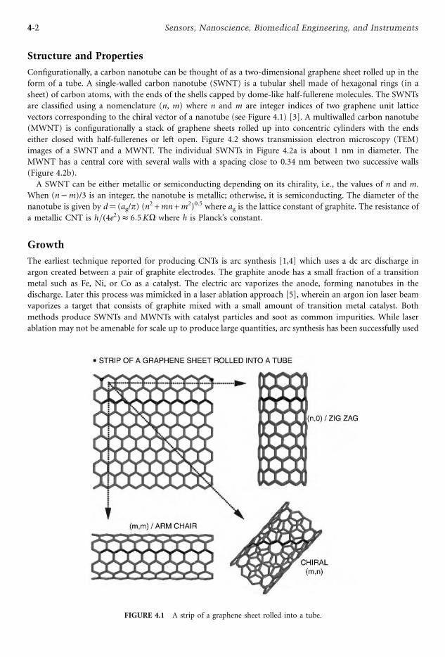
Structure and Properties
Configurationally, a carbon nanotube can be thought of as a two-dimensional graphene sheet rolled up in the
form of a tube. A single-walled carbon nanotube (SWNT) is a tubular shell made of hexagonal rings (in a
sheet) of carbon atoms, with the ends of the shells capped by dome-like half-fullerene molecules. The SWNTs
are classified using a nomenclature (n, m) where n and m are integer indices of two graphene unit lattice
vectors corresponding to the chiral vector of a nanotube (see Figure 4.1) [3]. A multiwalled carbon nanotube
(MWNT) is configurationally a stack of graphene sheets rolled up into concentric cylinders with the ends
either closed with half-fullerenes or left open. Figure 4.2 shows transmission electron microscopy (TEM)
images of a SWNT and a MWNT. The individual SWNTs in Figure 4.2a is about 1 nm in diameter. The
MWNT has a central core with several walls with a spacing close to 0.34 nm between two successive walls
(Figure 4.2b).
A SWNT can be either metallic or semiconducting depending on its chirality, i.e., the values of n and m.
When (n m)/3 is an integer, the nanotube is metallic; otherwise, it is semiconducting. The diameter of the
nanotube is given by d¼ (ag/p) (n2 +mn+m2)0.5 where ag is the lattice constant of graphite. The resistance of
a metallic CNT is h=ð4e2Þ 6:5KO where h is Planck’s constant.
Growth
The earliest technique reported for producing CNTs is arc synthesis [1,4] which uses a dc arc discharge in
argon created between a pair of graphite electrodes. The graphite anode has a small fraction of a transition
metal such as Fe, Ni, or Co as a catalyst. The electric arc vaporizes the anode, forming nanotubes in the
discharge. Later this process was mimicked in a laser ablation approach [5], wherein an argon ion laser beam
vaporizes a target that consists of graphite mixed with a small amount of transition metal catalyst. Both
methods produce SWNTs and MWNTs with catalyst particles and soot as common impurities. While laser
ablation may not be amenable for scale up to produce large quantities, arc synthesis has been successfully used
FIGURE 4.1 A strip of a graphene sheet rolled into a tube.
4-2 Sensors, Nanoscience, Biomedical Engineering, and Instruments
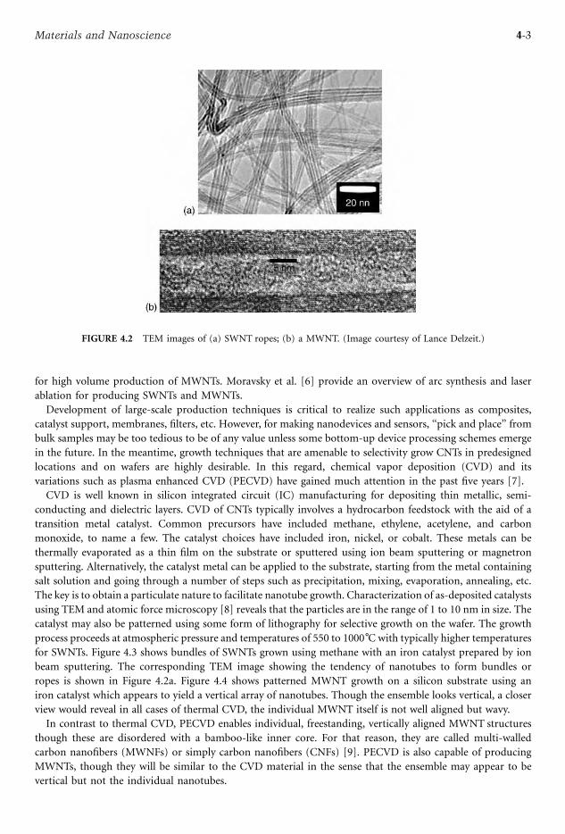
for high volume production of MWNTs. Moravsky et al. [6] provide an overview of arc synthesis and laser
ablation for producing SWNTs and MWNTs.
Development of large-scale production techniques is critical to realize such applications as composites,
catalyst support, membranes, filters, etc. However, for making nanodevices and sensors, ‘‘pick and place’’ from
bulk samples may be too tedious to be of any value unless some bottom-up device processing schemes emerge
in the future. In the meantime, growth techniques that are amenable to selectivity grow CNTs in predesigned
locations and on wafers are highly desirable. In this regard, chemical vapor deposition (CVD) and its
variations such as plasma enhanced CVD (PECVD) have gained much attention in the past five years [7].
CVD is well known in silicon integrated circuit (IC) manufacturing for depositing thin metallic, semi-
conducting and dielectric layers. CVD of CNTs typically involves a hydrocarbon feedstock with the aid of a
transition metal catalyst. Common precursors have included methane, ethylene, acetylene, and carbon
monoxide, to name a few. The catalyst choices have included iron, nickel, or cobalt. These metals can be
thermally evaporated as a thin film on the substrate or sputtered using ion beam sputtering or magnetron
sputtering. Alternatively, the catalyst metal can be applied to the substrate, starting from the metal containing
salt solution and going through a number of steps such as precipitation, mixing, evaporation, annealing, etc.
The key is to obtain a particulate nature to facilitate nanotube growth. Characterization of as-deposited catalysts
using TEM and atomic force microscopy [8] reveals that the particles are in the range of 1 to 10 nm in size. The
catalyst may also be patterned using some form of lithography for selective growth on the wafer. The growth
process proceeds at atmospheric pressure and temperatures of 550 to 1000 C with typically higher temperatures
for SWNTs. Figure 4.3 shows bundles of SWNTs grown using methane with an iron catalyst prepared by ion
beam sputtering. The corresponding TEM image showing the tendency of nanotubes to form bundles or
ropes is shown in Figure 4.2a. Figure 4.4 shows patterned MWNT growth on a silicon substrate using an
iron catalyst which appears to yield a vertical array of nanotubes. Though the ensemble looks vertical, a closer
view would reveal in all cases of thermal CVD, the individual MWNT itself is not well aligned but wavy.
In contrast to thermal CVD, PECVD enables individual, freestanding, vertically aligned MWNT structures
though these are disordered with a bamboo-like inner core. For that reason, they are called multi-walled
carbon nanofibers (MWNFs) or simply carbon nanofibers (CNFs) [9]. PECVD is also capable of producing
MWNTs, though they will be similar to the CVD material in the sense that the ensemble may appear to be
vertical but not the individual nanotubes.
FIGURE 4.2 TEM images of (a) SWNT ropes; (b) a MWNT. (Image courtesy of Lance Delzeit.)
4-3Materials and Nanoscience
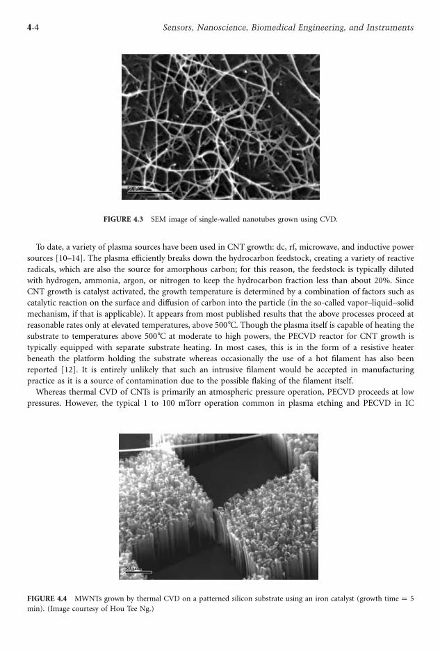
To date, a variety of plasma sources have been used in CNT growth: dc, rf, microwave, and inductive power
sources [10–14]. The plasma efficiently breaks down the hydrocarbon feedstock, creating a variety of reactive
radicals, which are also the source for amorphous carbon; for this reason, the feedstock is typically diluted
with hydrogen, ammonia, argon, or nitrogen to keep the hydrocarbon fraction less than about 20%. Since
CNT growth is catalyst activated, the growth temperature is determined by a combination of factors such as
catalytic reaction on the surface and diffusion of carbon into the particle (in the so-called vapor–liquid–solid
mechanism, if that is applicable). It appears from most published results that the above processes proceed at
reasonable rates only at elevated temperatures, above 500 C. Though the plasma itself is capable of heating the
substrate to temperatures above 500 C at moderate to high powers, the PECVD reactor for CNT growth is
typically equipped with separate substrate heating. In most cases, this is in the form of a resistive heater
beneath the platform holding the substrate whereas occasionally the use of a hot filament has also been
reported [12]. It is entirely unlikely that such an intrusive filament would be accepted in manufacturing
practice as it is a source of contamination due to the possible flaking of the filament itself.
Whereas thermal CVD of CNTs is primarily an atmospheric pressure operation, PECVD proceeds at low
pressures. However, the typical 1 to 100 mTorr operation common in plasma etching and PECVD in IC
FIGURE 4.3 SEM image of single-walled nanotubes grown using CVD.
FIGURE 4.4 MWNTs grown by thermal CVD on a patterned silicon substrate using an iron catalyst (growth time ¼ 5
min). (Image courtesy of Hou Tee Ng.)
4-4 Sensors, Nanoscience, Biomedical Engineering, and Instruments
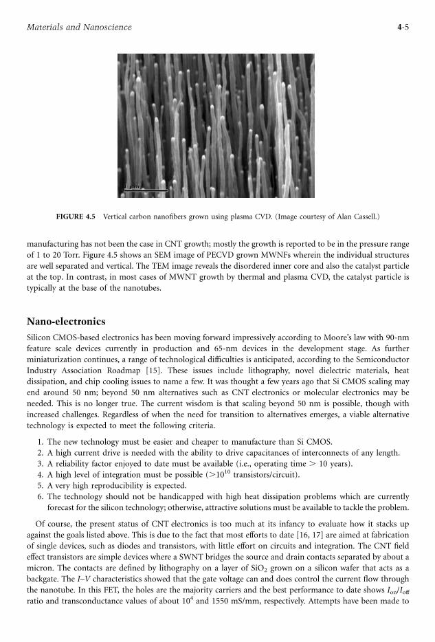
manufacturing has not been the case in CNT growth; mostly the growth is reported to be in the pressure range
of 1 to 20 Torr. Figure 4.5 shows an SEM image of PECVD grown MWNFs wherein the individual structures
are well separated and vertical. The TEM image reveals the disordered inner core and also the catalyst particle
at the top. In contrast, in most cases of MWNT growth by thermal and plasma CVD, the catalyst particle is
typically at the base of the nanotubes.
Nano-electronics
Silicon CMOS-based electronics has been moving forward impressively according to Moore’s law with 90-nm
feature scale devices currently in production and 65-nm devices in the development stage. As further
miniaturization continues, a range of technological difficulties is anticipated, according to the Semiconductor
Industry Association Roadmap [15]. These issues include lithography, novel dielectric materials, heat
dissipation, and chip cooling issues to name a few. It was thought a few years ago that Si CMOS scaling may
end around 50 nm; beyond 50 nm alternatives such as CNT electronics or molecular electronics may be
needed. This is no longer true. The current wisdom is that scaling beyond 50 nm is possible, though with
increased challenges. Regardless of when the need for transition to alternatives emerges, a viable alternative
technology is expected to meet the following criteria.
1. The new technology must be easier and cheaper to manufacture than Si CMOS.
2. A high current drive is needed with the ability to drive capacitances of interconnects of any length.
3. A reliability factor enjoyed to date must be available (i.e., operating time . 10 years).
4. A high level of integration must be possible (.1010 transistors/circuit).
5. A very high reproducibility is expected.
6. The technology should not be handicapped with high heat dissipation problems which are currently
forecast for the silicon technology; otherwise, attractive solutions must be available to tackle the problem.
Of course, the present status of CNT electronics is too much at its infancy to evaluate how it stacks up
against the goals listed above. This is due to the fact that most efforts to date [16, 17] are aimed at fabrication
of single devices, such as diodes and transistors, with little effort on circuits and integration. The CNT field
effect transistors are simple devices where a SWNT bridges the source and drain contacts separated by about a
micron. The contacts are defined by lithography on a layer of SiO2 grown on a silicon wafer that acts as a
backgate. The I–V characteristics showed that the gate voltage can and does control the current flow through
the nanotube. In this FET, the holes are the majority carriers and the best performance to date shows Ion/Ioffratio and transconductance values of about 104 and 1550 mS/mm, respectively. Attempts have been made to
FIGURE 4.5 Vertical carbon nanofibers grown using plasma CVD. (Image courtesy of Alan Cassell.)
4-5Materials and Nanoscience
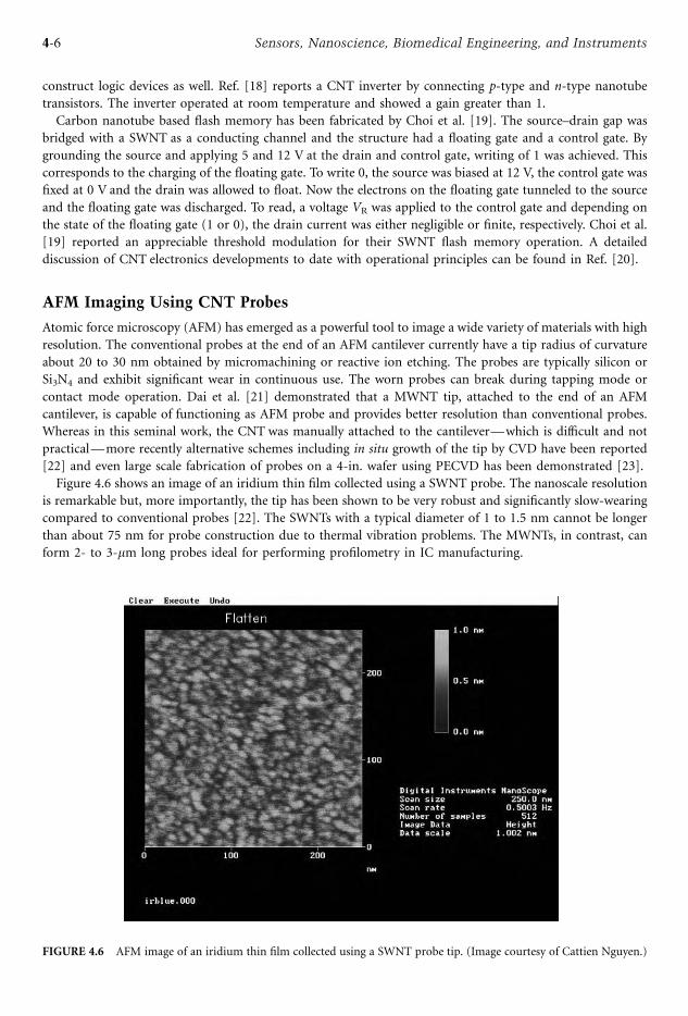
construct logic devices as well. Ref. [18] reports a CNT inverter by connecting p-type and n-type nanotube
transistors. The inverter operated at room temperature and showed a gain greater than 1.
Carbon nanotube based flash memory has been fabricated by Choi et al. [19]. The source–drain gap was
bridged with a SWNT as a conducting channel and the structure had a floating gate and a control gate. By
grounding the source and applying 5 and 12 V at the drain and control gate, writing of 1 was achieved. This
corresponds to the charging of the floating gate. To write 0, the source was biased at 12 V, the control gate was
fixed at 0 V and the drain was allowed to float. Now the electrons on the floating gate tunneled to the source
and the floating gate was discharged. To read, a voltage VR was applied to the control gate and depending on
the state of the floating gate (1 or 0), the drain current was either negligible or finite, respectively. Choi et al.
[19] reported an appreciable threshold modulation for their SWNT flash memory operation. A detailed
discussion of CNT electronics developments to date with operational principles can be found in Ref. [20].
AFM Imaging Using CNT Probes
Atomic force microscopy (AFM) has emerged as a powerful tool to image a wide variety of materials with high
resolution. The conventional probes at the end of an AFM cantilever currently have a tip radius of curvature
about 20 to 30 nm obtained by micromachining or reactive ion etching. The probes are typically silicon or
Si3N4 and exhibit significant wear in continuous use. The worn probes can break during tapping mode or
contact mode operation. Dai et al. [21] demonstrated that a MWNT tip, attached to the end of an AFM
cantilever, is capable of functioning as AFM probe and provides better resolution than conventional probes.
Whereas in this seminal work, the CNT was manually attached to the cantilever—which is difficult and not
practical—more recently alternative schemes including in situ growth of the tip by CVD have been reported
[22] and even large scale fabrication of probes on a 4-in. wafer using PECVD has been demonstrated [23].
Figure 4.6 shows an image of an iridium thin film collected using a SWNT probe. The nanoscale resolution
is remarkable but, more importantly, the tip has been shown to be very robust and significantly slow-wearing
compared to conventional probes [22]. The SWNTs with a typical diameter of 1 to 1.5 nm cannot be longer
than about 75 nm for probe construction due to thermal vibration problems. The MWNTs, in contrast, can
form 2- to 3-mm long probes ideal for performing profilometry in IC manufacturing.
FIGURE 4.6 AFM image of an iridium thin film collected using a SWNT probe tip. (Image courtesy of Cattien Nguyen.)
4-6 Sensors, Nanoscience, Biomedical Engineering, and Instruments
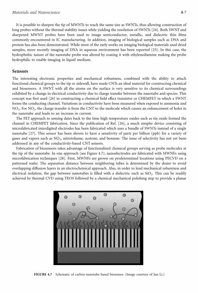
It is possible to sharpen the tip of MWNTs to reach the same size as SWNTs, thus allowing construction of
long probes without the thermal stability issues while yielding the resolution of SWNTs [24]. Both SWNTand
sharpened MWNT probes have been used to image semiconductor, metallic, and dielectric thin films
commonly encountered in IC manufacturing. In addition, imaging of biological samples such as DNA and
protein has also been demonstrated. While most of the early works on imaging biological materials used dried
samples, more recently imaging of DNA in aqueous environment has been reported [25]. In this case, the
hydrophobic nature of the nanotube probe was altered by coating it with ethylenediamine making the probe
hydrophilic to enable imaging in liquid medium.
Sensors
The interesting electronic properties and mechanical robustness, combined with the ability to attach
functional chemical groups to the tip or sidewall, have made CNTs an ideal material for constructing chemical
and biosensors. A SWNT with all the atoms on the surface is very sensitive to its chemical surroundings
exhibited by a change in electrical conductivity due to charge transfer between the nanotube and species. This
concept was first used [26] in constructing a chemical field effect transistor or CHEMFET in which a SWNT
forms the conducting channel. Variations in conductivity have been measured when exposed to ammonia and
NO2. For NO2, the charge transfer is from the CNT to the molecule which causes an enhancement of holes in
the nanotube and leads to an increase in current.
The FET approach to sensing dates back to the time high temperature oxides such as tin oxide formed the
channel in CHEMFET fabrication. Since the publication of Ref. [26], a much simpler device consisting of
microfabricated interdigited electrodes has been fabricated which uses a bundle of SWNTs instead of a single
nanotube [27]. This sensor has been shown to have a sensitivity of parts per billion (ppb) for a variety of
gases and vapors such as NO2, nitrotoluene, acetone, and benzene. The issue of selectivity has not yet been
addressed in any of the conductivity-based CNT sensors.
Fabrication of biosensors takes advantage of functionalized chemical groups serving as probe molecules at
the tip of the nanotube. In one approach (see Figure 4.7), nanoelectrodes are fabricated with MWNFs using
microfabrication techniques [28]. First, MWNFs are grown on predetermined locations using PECVD on a
patterned wafer. The separation distance between neighboring tubes is determined by the desire to avoid
overlapping diffusion layers in an electrochemical approach. Also, in order to lend mechanical robustness and
electrical isolation, the gap between nanotubes is filled with a dielectric such as SiO2. This can be readily
achieved by thermal CVD using TEOS followed by a chemical mechanical polishing step to provide a planar
FIGURE 4.7 Schematic of carbon nanotube based biosensor. (Image courtesy of Jun Li.)
4-7Materials and Nanoscience

top surface with CNTends exposed. These CNTends can then be derivatized with DNA, PNA, or other probe
molecules. Li et al. [28] performed cyclovoltammetry measurements and showed a capability of less than 1000
target molecules. This limit approaches that of laser-based fluorescence techniques and the approach offers a
high degree of miniaturization and multiplex operation in molecular diagnosis. The sensor platform approach
is amenable for developing handheld diagnostic devices for chemical diagnostics, biothreat detection, and
similar applications.
Field Emission
CNTs have been shown to be excellent field emitters in a number of studies and a review can be found in
Ref. [29]. The high aspect ratio of the CNTs and small tip radius of curvature are ideal for field emission. The
emission has been observed at fields less than 1 V/mm and current densities as high as 1 A/cm2 have been
obtained. All forms of nanotubes—SWNTs, MWNTs, and MWNFs—and grown by all methods have been
shown to be useful in field emission applications although emission characteristics vary with structure,
preparation technique and impurity level.
Applications for CNT field emitters are broad and indeed, any application requiring an electron source is a
candidate. Currently the biggest driver for the CNT field emission research is the potential to develop flat
panel television displays. In a CNT-based field emission display (FED), controlled bombardment of electrons
on a phosphor induces local emission, much like in a cathode ray tube (CRT). However, unlike in a CRT, the
CNT–FED will have numerous electron sources, indeed one per pixel. The absence of beam scanning inherent
in a CRT allows close placement of the electron source to the screen thus enabling a thin display. Currently
several companies in Korea and Japan have developed prototype flat panel displays based on CNT–FED as
large as 40-in. screen. Other CNT–FED applications include vacuum microelectronics, microwave amplifiers,
electric propulsion, and x-ray tubes.
Summary
The interesting properties of carbon nanotubes have spurred an extraordinary amount of research activity.
Much progress has been made in CNT growth by a variety of techniques, but as of now no control on the
chirality of the CNTs during growth is possible. Characterization techniques to examine the grown structure
have advanced rapidly and significant efforts continue across the world to measure electrical, mechanical,
optical, thermal, magnetic, and other properties. Application development has been receiving the strongest
attention with focus on nanoelectronics, sensors, field emission, scanning probes, actuators, gas adsorption
and storage, and composites. All of these activities are in their early stages and there are no commercial
products with mass market appeal in the market now. The CNT community believes that this will change in
a decade.
Acknowledgment
The author gratefully acknowledges his colleagues at NASA Ames Research Center for Nanotechnology for
much of the material presented in this chapter.
References
1. S. Iijima, Nature, 354, 56, 1991.
2. M. Meyyappan, Ed., Carbon Nanotubes: Science and Applications, Boca Raton, FL: CRC Press, 2004.
3. J. Han, chap. 1 in Ref. [2].
4. T. W. Ebbesen and P.M. Ajayan, Nature, 358, 220, 1992.
5. T. Guo et al., Chem. Phys. Lett., 243, 49, 1995.
6. A.P. Moravsky, E.M. Wexler, R.O. Loutfy, chap. 3 in Ref. [2].
7. M. Meyyappan, chapter 4 in Ref. [3]; see references therein.
8. L. Delzeit et al., Chem. Phys. Lett., 348, 368, 2001.
4-8 Sensors, Nanoscience, Biomedical Engineering, and Instruments
9. M. Meyyappan et al., Plasma Sour. Sci. Technol. 12, 205, 2003.
10. V.I. Merkulov et al., Appl. Phys. Lett., 76, 3555, 2000.
11. M. Chhowalla et al., J. Appl. Phys., 90, 5308, 2001.
12. Z.F. Ren et al., Science, 282, 1105, 1998.
13. C. Bower et al., Appl. Phys. Lett., 77, 830, 2000.
14. K. Matthews et al., J. Nanosci. Nanotech. 2, 475, 2002.
15. International Technology Roadmap for Semiconductors, San Jose, CA: Semiconductor Industry
Association, 2001.
16. S.J. Tans et al., Nature, 393, 49, 1998.
17. R. Martel et al., Appl. Phys. Lett., 76, 2447, 1998.
18. X. Liu et al., Appl. Phys. Lett., 79, 3329, 2001.
19. W.B. Choi et al., Appl. Phys. Lett., 82, 275, 2003.
20. T. Yamada, chap. 7 in Ref. [2].
21. H. Dai et al., Nature, 384, 147, 1996.
22. C.V. Nguyen et al., Nanotechnology, 12, 363, 2001.
23. Q. Ye et al., NanoLett., 2004.
24. C.V. Nguyen et al., J. Phys. Chem. B, 108, 2816, 2004.
25. R. Stevens et al., IEEE Trans. Nanobio. Technol., 3, 56, 2004.
26. J. Kong et al., Science, 287, 622, 2000.
27. J. Li et al., NanoLett., 3, 929, 2003.
28. J. Li et al., NanoLett., 3, 597, 2003.
29. P. Sarrazin, chap. 8 in Ref. [2].
4.2 Modeling MEMS and NEMS
John Pelesko
Mathematical modeling of micro- and nano-electromechanical systems (MEMS and NEMS) is an essential
part of the design and optimization process. The complexity of typical MEMS and NEMS devices often
necessitates the study of coupled-domain problems. The small scale of such devices leads to novel balances in
appropriate continuum theories when continuum theory is still valid. At the extreme limits of scale, modeling
tools such as molecular dynamics become invaluable.
Micro- and Nano-Electromechanical Systems
Enter the word ‘‘nanotechnology’’ into the Googlee search engine and you will be inundated with more than
1.5 million hits. The acronym for micro-electromechanical systems, i.e., MEMS, returns slightly fewer at
857,000, while the word ‘‘nanoscience’’ returns a still respectable 134,000 sites.1 This is just a crude measure of
the popularity and importance of micro- and nanoscale science, but it makes clear the present overwhelming
interest in these fields from both the scientific and lay communities.
The popularity of MEMS and NEMS technology is made more amazing by the fact that both fields are still
relatively young. The roots of microsystem technology lie in technological developments accompanying
World War II. In particular, wartime research in radar stimulated research in the synthesis of pure semi-
conducting materials. These materials, especially silicon, became the platform on which MEMS technology
was built.
Both MEMS researchers and nanotechnology proponents point to Richard Feynman’s famous ‘‘There’s
plenty of room at the bottom’’ lecture as a seminal event in their respective fields. Showing remarkable
prescience, in 1959 Feynman anticipated much of the next four decades of research in MEMS and NEMS:
1Googlee searches performed July 2004.
4-9Materials and Nanoscience

It is a staggeringly small world that is below. In the year 2000, when they look back at this age,
they will wonder why it was not until the year 1960 that anybody began to seriously move in this
direction.
While Feynman’s lecture inspired a few immediate developments, it was not until 5 years later that MEMS
technology officially arrived. In 1964, H.C. Nathanson and his colleagues at Westinghouse produced the first
batch fabricated MEMS device. Their resonant gate transistor exhibited all of the features of modern MEMS.
Especially notable is the key role played by mathematical modeling in the development of the resonant gate
transistor. In fact, almost half of Nathanson’s seminal paper concerns the development of a mathematical
model. Today, the role of mathematical modeling in MEMS and NEMS is as important as ever. The high cost
in both time and money needed to fabricate and test most MEMS and NEMS devices makes mathematical
modeling an essential part of the design and optimization process. Further, an effective mathematical model
provides the micro- or nanoresearcher with a new window into the small world below.
The Science of Scale
It is almost ridiculously obvious to state that the difference between macroscale and microscale engineering is
one of size. Yet, this simple observation is crucial for understanding why and how micro- and nanoscale
systems behave. It cannot be stated too forcefully: things change as length scales change. Consider taking a hot
Thanksgiving turkey out of the oven. The aluminum foil covering the turkey cools from 400 F to room
temperature in about a minute, while the turkey itself stays hot for hours. The difference is one of scale. The
relevant length scale for the foil is its thickness, hence the ratio of the foil’s volume to surface area is very small.
Little thermal energy can be held, while lots of thermal energy can be convected away. In contrast, the relevant
length scale for the turkey is much larger and its volume to surface area ratio much closer to one.
Scaling effects play a role in studying every aspect of MEMS and NEMS. In the microworld inertial effects
are negligible compared to viscous effects, heat transfer is a fast process, and electrostatic forces dominate over
almost every other type of force. The relative importance of various effects and how things change as system
size changes can often be computed from simple scaling arguments. This is an important first step in the
modeling process.
As an example of these types of arguments, let us examine how we would approach the study of a thermal-
elastic actuator. A typical such system is sketched in Figure 4.8. In this design, pioneered by Y.C. Tai and his
TABLE 4.1 Landmarks in the History of MEMS and NEMSa
1940s Radar drives the development of pure semiconductors.
1959 Richard P. Feynman’s famous ‘‘There’s plenty of room at the bottom’’ lecture.
1960 Planar batch-fabrication process invented.
1964 H.C. Nathanson and team at Westinghouse produce the resonant gate transistor, the first batch-fabricated
MEMS device.
1970 The microprocessor is invented, driving the demand for integrated circuits ever higher.
1979 The first micromachined accelerometer is developed at Stanford University.
1981 K. Eric Drexler’s article, ‘‘Protein design as a pathway to molecular manufacturing,’’ is published in the
Proceedings of the National Academy of Sciences. This is arguably the first journal article on molecular
nanotechnology to appear.
1982 The scanning tunneling microscope is invented.
1984 The polysilicon surface micromachining process is developed at the University of California, Berkeley.
MEMS and integrated circuits can be fabricated together for the first time.
1985 The ‘‘Buckyball’’ is discovered.
1986 The atomic force microscope is invented.
1991 The carbon nanotube is discovered.
1996 Richard Smalley develops a technique for producing carbon nanotubes of uniform diameter.
2000s The number of MEMS devices and applications continually increases. National attention is focused on
funding nanotechnology research and education.
aReprinted with permission fromModeling MEMS and NEMS, Pelesko and Bernstein, Chapman and Hall/CRC Press, Boca Raton,FL, 2002.
4-10 Sensors, Nanoscience, Biomedical Engineering, and Instruments
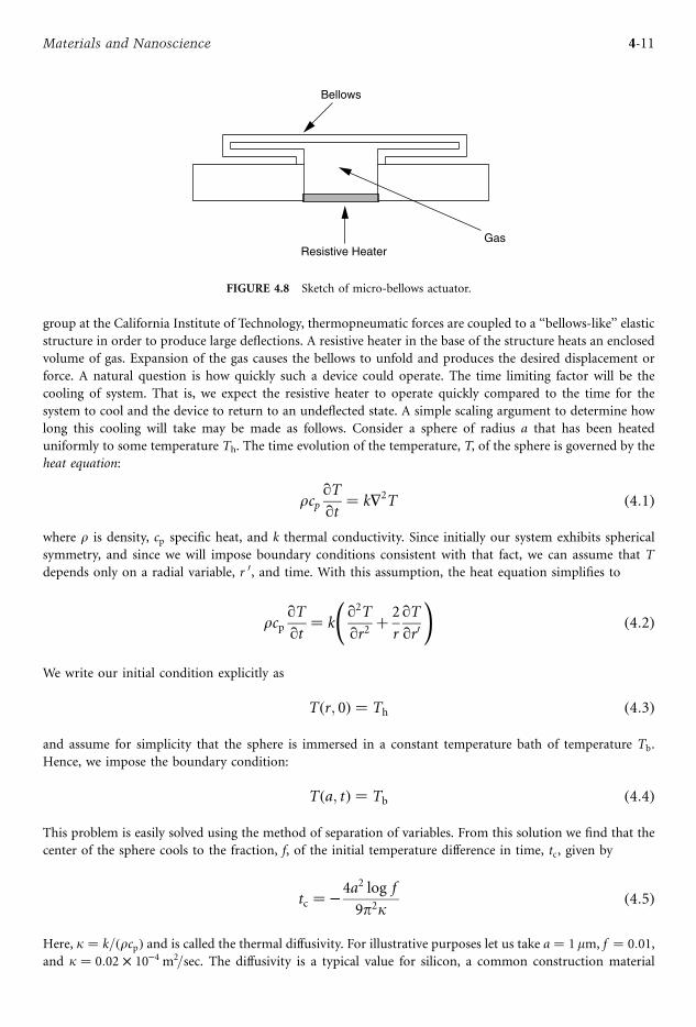
group at the California Institute of Technology, thermopneumatic forces are coupled to a ‘‘bellows-like’’ elastic
structure in order to produce large deflections. A resistive heater in the base of the structure heats an enclosed
volume of gas. Expansion of the gas causes the bellows to unfold and produces the desired displacement or
force. A natural question is how quickly such a device could operate. The time limiting factor will be the
cooling of system. That is, we expect the resistive heater to operate quickly compared to the time for the
system to cool and the device to return to an undeflected state. A simple scaling argument to determine how
long this cooling will take may be made as follows. Consider a sphere of radius a that has been heated
uniformly to some temperature Th. The time evolution of the temperature, T, of the sphere is governed by the
heat equation:
rcpqTqt
¼ kH2T ð4:1Þwhere r is density, cp specific heat, and k thermal conductivity. Since initially our system exhibits spherical
symmetry, and since we will impose boundary conditions consistent with that fact, we can assume that T
depends only on a radial variable, r 0, and time. With this assumption, the heat equation simplifies to
rcpqTqt
¼ kq2Tqr2
þ 2
r
qTqr0
!ð4:2Þ
We write our initial condition explicitly as
Tðr; 0Þ ¼ Th ð4:3Þ
and assume for simplicity that the sphere is immersed in a constant temperature bath of temperature Tb.
Hence, we impose the boundary condition:
Tða; tÞ ¼ Tb ð4:4Þ
This problem is easily solved using the method of separation of variables. From this solution we find that the
center of the sphere cools to the fraction, f, of the initial temperature difference in time, tc, given by
tc ¼ 4a2 log f
9p2kð4:5Þ
Here, k ¼ k=ðrcpÞ and is called the thermal diffusivity. For illustrative purposes let us take a ¼ 1 mm, f ¼ 0:01,
and k ¼ 0:02 10 4 m2=sec. The diffusivity is a typical value for silicon, a common construction material
Bellows
Resistive HeaterGas
FIGURE 4.8 Sketch of micro-bellows actuator.
4-11Materials and Nanoscience

in MEMS. We find tc 10 7 sec. Our sphere cools in a tenth of a microsecond. Assuming the sphere could be
heated just as quickly, we find that our device can be operated at 5000 KHz.
This calculation represents the first step in the modeling process, i.e., performing a simple analysis in order
to determine design feasibility. The estimate obtained of operating frequency is not meant to be definitive, but
rather represents an order of magnitude calculation. If the order of magnitude of the estimates is in the desired
range, more detailed models can now be constructed to guide the design process. Many more examples of
simple scaling arguments may be found in Trimmer (1997) and Pelesko (2002).
Modeling Approaches
Once design feasibility has been ascertained, it is often desirable to create a more detailed and more realistic
model of the system under consideration. A good model can guide design, help optimize the design, and
explain phenomena observed during experimentation. There are no hard and fast rules concerning what
modeling tools to use when studying MEMS and NEMS. Rather, the MEMS/NEMS researcher must be open
to learning and employing a variety of tools as the situation warrants. There are, however, some tools that have
proven of wide utility. We highlight some of these here.
Continuum Mechanics
The vast majority of mathematical models of MEMS and NEMS devices are based on the equations of
continuum mechanics. The key test for the validity of continuum mechanics in the study of a particular MEMS/
NEMS system is whether or not molecular details of the system may be ignored. Can the continuum hypothesis
be assumed? If molecular details may be ignored then quantities such as temperature, pressure, and stress, can
be treated as smoothly varying functions of spatial coordinates. If the continuum hypothesis is not valid, or
quantum effects are important, an alternative approach is called for. Some alternative approaches are discussed
below. Here, we review the principal equations of continuum mechanics. We note that the choice of boundary
and initial conditions for these equations is highly dependent on the situation under consideration. Detailed
discussions of boundary and initial conditions for the equations of continuum mechanics may be found in
Segel (1987) and Lin (1988).
We have already encountered the heat equation which characterizes the thermal behavior of a body or
a fluid:
rcpqTqt
¼ kH2T ð4:6Þ
This equation expresses conservation of energy. As written a homogeneous isotropic material is assumed.
If the medium is inhomogeneous or anisotropic, the proper equation governing heat flow is
rcpqTqt
¼ H kHT ð4:7Þ
Anisotropy may be modeled by treating k as a tensor. This allows the heat flux to vary as a function of
direction within the material. The inhomogeneous nature of a material may be modeled by treating r, cp, andk as functions of position.
The elastic behavior of a solid body is characterized in terms of stress and strain. The stress in a solid body is
expressed in terms of the stress tensor, sij. If you are unfamiliar with tensors, you can think of sij as simplybeing a 3 3 matrix:
s11 s12 s13s21 s22 s23s31 s32 s33
0@ 1A ð4:8Þ
The ijth component of this matrix, sij, denotes the force per unit area in the direction i exerted on a surfaceelement with normal in the j direction. Balance of angular momentum within an elastic body requires that the
4-12 Sensors, Nanoscience, Biomedical Engineering, and Instruments

stress tensor be symmetric, i.e.:
sij ¼ sji ð4:9Þ
Or in matrix notation
sij ¼s11 s12 s13s12 s22 s23s13 s23 s33
0@ 1A ð4:10Þ
so that we have only six independent components of the stress tensor. The strain in a solid body is also
expressed in terms of a tensor, called the strain tensor, and is denoted eij. For small displacements, the straintensor is related to displacements of the elastic body by
eij ¼ 1
2
quiqxj
þ qujqxi
!ð4:11Þ
Here, ui is the ith component of the displacement vector and the partial derivatives are taken with respect to
the directions x1, x2, and x3 in a Cartesian coordinate system. Note that Equation (4.11) is only valid for
small displacements. This equation has been linearized by ignoring quadratic terms. In general, the strain
tensor is
eij ¼ 1
2
quiqxj
þ qujqxi
þ qukqxi
qukqxj
!ð4:12Þ
We have assumed the Einstein summation convention. This simply says that when you see a repeated index, it
denotes summation over that index. Above, the repeated index of k indicates summation over k. The
approximation of small displacements allows us to use Equation (4.11) in place of Equation (4.12). The basic
equation of elasticity comes from applying conservation of momentum. That is, we apply Newton’s second law
to an appropriate control volume and obtain
rq2uiqt2
¼ qsijqxj
þ fi ð4:13Þ
where r is the density of the body and fi is the body force per unit volume. For instance, in modeling an
electrostatically actuated device, fi would be computed from electrostatic forces while in a magnetic device fiwould be computed from magnetic forces. Note that Equation (4.13) is really a set of three equations, one for
each of the components of the displacement vector.
To close the system we make a constitutive assumption. We assume a generalized Hooke’s law:
sij ¼ 2meij þ lekkdij ð4:14Þ
Equation (4.14) assumes that stress and strain are linearly related. Here, m and l are the Lame constants whiledij is called the Kronecker delta. In matrix terms, dij is simply the 3 3 identity matrix. The Lame constants are
related to the more familiar Young’s modulus:
E ¼ mð2mþ 3lÞlþ m
ð4:15Þ
4-13Materials and Nanoscience

and Poisson ratio:
n ¼ l2ðlþ mÞ ð4:16Þ
Hence, Equation (4.14) may be rewritten as
Eeij ¼ ð1þ nÞsij nskkdij ð4:17Þ
Now, substituting Equation (4.14) into Equation (4.13), we obtain the Navier equations of elasticity:
rq2uiqt2
¼ qqxj
ð2meij þ lekkdijÞ ð4:18Þ
Eliminating the strain tensor in favor of the displacement vector and using vector notation yields
rq2uqt2
¼ mH2uþ ðmþ lÞHðH uÞ þ f ð4:19Þ
Equation (4.19) is a set of equations called the Navier equations of linear elasticity.
When the elastic and thermal behaviors of a body are coupled, the equations of linear thermoelasticity are
called for. In thermoelasticity, we incorporate a term in the heat equation that reflects the fact that elastic
energy is converted into thermal energy. The modified heat equation is
rcpqTqt
¼ H kHT að3lþ 2mÞT0 qekkqt ð4:20Þ
Here, a is called the coefficient of thermal expansion and T0 is a suitably defined reference temperature. Thedefinition of the strain, eij, remains unchanged from linear elasticity:
eij ¼ 1
2
quiqxj
þ qujqxi
!ð4:21Þ
as does the balance of linear momentum:
rq2uiqt2
¼ qsijqxj
þ fi ð4:22Þ
Also, as in linear elasticity, the stress tensor is symmetric sij ¼ sji, reflecting the balance of angular
momentum. The major modification to the linear elastic theory is to the constitutive law. A modified Hooke’s
law known as the Duhamel–Neumann relation is introduced. This modified Hooke’s law contains a term
expressing the fact that a rise in temperature creates a stress within a material:
sij ¼ 2meij þ ldijekk dijað3lþ 2mÞðT T0Þ ð4:23Þ
Again, we have assumed the summation convention. Equation (4.20) to Equation (4.23) are known as the
equations of linear thermoelasticity.
As with the Navier equations describing the motion of elastic bodies, the behavior of a fluid is characterized
in terms of stress and strain. In fluids, however, in addition to conservation of momentum, we also have an
4-14 Sensors, Nanoscience, Biomedical Engineering, and Instruments

equation derived from the principle of conservation of mass. If r denotes the density of fluid and ui is a vectorof fluid velocities, whose ith component is fluid velocity in direction i, then conservation of mass says
qrqtþ uj
qrqxj
þ rquiqxi
¼ 0 ð4:24Þ
In contrast with elasticity, the reader should keep in mind that here we are working with velocities rather than
displacements. This implies that it is convenient to define the strain rate tensor as opposed to the strain tensor.
In particular, we define
qeijqt
¼ 1
2
quiqxj
þ qujqxi
!ð4:25Þ
Stress in a fluid is expressed in terms of the stress tensor sij, which, as with elasticity, may be thought of as the3 3 matrix:
s11 s12 s13s21 s22 s23s31 s32 s33
0@ 1A ð4:26Þ
The ijth component of this matrix, sij again, denotes the force per unit area in the direction i exerted on a
surface element with normal in the j direction. The stress tensor is related to the rate of strain tensor through
sij ¼ pdij þ 2m _eeijþl _eekk dij ð4:27Þ
Here, the dot denotes differentiation with respect to time, p is the pressure in the fluid, m is the dynamic fluidviscosity, and l is a second viscosity coefficient. Recall that repeated indices indicate summation and that dijdenotes the Kroneker delta or 3 3 identity matrix. The equation of conservation of momentum can now be
written as
rquiqt
þ rujquiqxj
¼ rFi þqsijqxj
ð4:28Þ
Using Equation (4.27) in Equation (4.28), we obtain
rquiqt
þ rujquiqxj
¼ rFiqpqxi
þ qqxj
ð2m _eeijþl _eekk dijÞ ð4:29Þ
Equation (4.29) is usually called the Navier–Stokes equation of motion and Equation (4.24) and Equation
(4.29) are called the Navier–Stokes equations. We may rewrite the Navier–Stokes equations in vector form:
qrqtþ H ðruÞ ¼ 0 ð4:30Þ
rquqtþ rðu HÞuþ Hp mH2u ðlþ mÞHðH uÞ ¼ f ð4:31Þ
In Equation (4.31), we have eliminated the strain rate tensor in favor of the velocity vector and relabeled the
body force vector as f.
4-15Materials and Nanoscience
Equation (4.30) and Equation (4.31), the Navier–Stokes equations for a viscous compressible fluid, are a
system of four coupled nonlinear partial differential equations. Notice, however, that the system contains five
unknown functions. The pressure, the density, and the three components of the velocity vector field are all
unknown. To close this system one usually appends the equation of conservation of energy to the Navier–
Stokes equations. This introduces one more equation and one more unknown function, the temperature T.
The system is then completed by introducing an equation of state which relates r, p, and T. Various
simplifications of the Navier–Stokes equations are possible. In particular, the so called Stokes equations are
often of relevance in microfluidics.
Electromagnetic phenomena are described by Maxwell’s equations. This system of four coupled
partial differential equations describes the spatial and temporal evolution of the four vector fields, E, D, B,
and H:
H D ¼ re0
ð4:32Þ
H E ¼ 1
c
qBqt
ð4:33Þ
H B ¼ 0 ð4:34Þ
H H ¼ 1
c
qDqtþ J ð4:35Þ
Here, r is the electrical charge density, J is the current density, and c is the speed of light in vacuum. To
complete the description of the dynamics of charged particles in the presence of electromagnetic fields we
must also supply the Lorenz force law:
F ¼ q Eþ v Bð Þ ð4:36Þ
where q is the electric charge of the particle and v its velocity. Note that the conservation of charge:
qrqtþ H J ¼ 0 ð4:37Þ
is a consequence of Maxwell’s equations.
The Maxwell equations are a system of 8 equations in the 12 components of E, D, B, and H. To close
the system the constitutive relations of the materials involved are necessary. For linear materials these are
usually written:
Di ¼ eijEj ð4:38Þ
Bi ¼ mijHj ð4:39Þ
The tensors eij (the permittivity tensor) and mij (the magnetic permeability tensor) are properties of materialswhich contain information about how they respond to the presence of external electric and magnetic fields.
Note that this form does not apply to materials with permanent electric or magnetic moments (ferroelectric
and ferromagnetic materials, respectively).
As an example, many materials respond to an electric field by generating a dipole moment. In addition, the
dipole moment is independent of the direction of the applied field and its position in space. In this case, the
material is said to be homogeneous and isotropic as well as linear and the permittivity tensor takes on the simple
4-16 Sensors, Nanoscience, Biomedical Engineering, and Instruments

form eij ¼ edij; hence,
D ¼ eE ð4:40Þ
In this case, e is the called the dielectric constant of the material. Note that while a large number of materials(called, naturally, dielectrics) fall into this category, most magnetic materials used in current technology are
ferromagnetic as well as having a nonlinear response to external magnetic fields. Paramagnetic and diamagnetic
materials, which do not have permanent magnetic moments and are linear in their response, are more the
exception than the rule.
Mathematical models of MEMS and NEMS devices usually involve coupled domains. For example, a system
may be thermoelectric and its study requires a model using both the heat equation and Maxwell’s equations
coupled through appropriate boundary and source terms. Perhaps the most prevalent coupled domains in
MEMS systems are thermal–elastic systems such as thermoelastic actuators, electrostatic–elastic systems such
as accelerometers or electrostatic actuators, and elastic–fluidic systems such as micropumps. Detailed
examples of such models may be found in Pelesko (2002). One of the more interesting aspects of modeling
MEMS and NEMS again is a consequence of scale. When a continuum based mathematical model has been
constructed, the next step, as with all engineering theories, is to simplify the equations where possible. This
involves determining the relative importance of various terms in the mathematical model. The small length
scales involved in MEMS and NEMS often lead to novel balances of terms in continuum models. For example,
inertial terms are often negligible whereas in the macro world they are usually dominant. This and other scale
effects makes continuum modeling of MEMS and NEMS systems exciting and different than macro-
engineering.
Other Tools
One of the key landmarks in the history of the development of MEMS and NEMS came in 1985 with the
discovery by Curl, Kroto, and Smalley of C60, the carbon ‘‘Buckeyball structure.’’ The importance of this
discovery was recognized almost immediately by the scientific community and, in 1996, the trio received the
Nobel Prize for their work. The importance of the follow up discovery of carbon nanotubes promises to eclipse
even the discovery of C60. Nanotubes, often visualized as sheets of ‘‘chicken wire’’ rolled into a cylinder, exhibit
fascinating thermal, elastic, and electrical properties. Technological developments based on nanotubes are
proceeding apace.
When constructing a mathematical model of a device based on nanotube technology, molecular effects may
become important. It is important to note the words ‘‘may become.’’ This too is a question of scale. If, for
example, one is interested in the bending of a nanotube serving as part of a nanotweezer system, the Navier
equations of elasticity may be the basis for a perfectly valid model describing the elastic deflections of the tube.
If, however, one is interested in the motion of a nanotube-based gear where individual atoms bound to the
nanotube surface serve as gear teeth, a molecular scale model may be in order. In the latter case, molecular
dynamics based simulation is often the only way to go.
In a typical molecular dynamics (MD) simulation, the location of each individual molecule is tracked.
A potential, such as the Lenard–Jones potential, is used to model particle–particle interactions. Static
configurations are then obtained by minimizing the energy of the system, while dynamic behaviors are
simulated using classical mechanics for each particle and the appropriate potential to simulate particle–
particle interactions. MD simulations are often computationally quite costly; however, rapid progress in
nanoscale MD simulations is being made. The reader is referred to the listing below for further reading in
this area.
Another area of micro- and nanotechnology showcasing rapidly developing mathematical modeling tools is
the field of self-assembly. Our ability to fully exploit the potential of micro- and nano-electromechanical
systems (MEMS and NEMS) technology is to a large extent dependent upon our capacity to efficiently
fabricate and organize MEMS and NEMS devices and systems. Fabrication technologies used in MEMS are
almost wholly derived from analogous technology used in the fabrication of integrated circuits. While this
4-17Materials and Nanoscience

approach has been quite successful for MEMS, the feasibility of pushing this technology downward toward
the nanoscale is doubtful. Rather, the few true NEMS devices fabricated have relied on costly, time-
consuming, ad hoc methods, which do not easily scale to allow the production of batches of devices. Similarly,
while many MEMS devices and several NEMS devices have been produced and even commercialized, the
promise of MEMS and NEMS systems remains largely unfulfilled. The ideal of having thousands or tens of
thousands of individual MEMS/NEMS devices working together as part of a system has yet to be widely
realized.
To address these concerns, researchers in MEMS and NEMS have recently turned toward the study of self-
assembly (SA) and self-organization (SO). Of course, the study of SA and SO did not originate with the
MEMS and NEMS community, but rather has been an intense topic of research in many fields (Langton,
1995). It is worth noting, however, that the engineering perspective of the MEMS and NEMS community
leads to a different take and different set of questions for studies of self-assembly and self-organization.
Rather than attempting to describe the behavior of complex systems by assigning simple rules to individual
agents, the MEMS and NEMS researcher seeks to construct a system with a desired complex behavior.
The necessities of working on the micro- or nanoscale, make the individual-agent, simple-rules, emergent
behavior approach particularly attractive. The mathematical tools used to model the self-assembly process are
often very different than the tools used to model the behavior of an individual MEMS or NEMS device.
A common approach borrows techniques from theoretical computer science. A set of rules, or a ‘‘grammar,’’
defining how elements of the system can combine is constructed. Study of this grammar can then answer a
myriad of questions about the self-assembling system. For example, what is the achievable complexity of a
self-assembled system evolving according to a given rules set? Or, what is the statistical distribution of
expected assemblies?
Of course, molecular dynamics and grammar based models are but two of the many new techniques being
employed by MEMS and NEMS researchers. As the fields progress, and new challenges arise, undoubtedly
those in the MEMS and NEMS field will draw on an ever widening range of mathematical tools.
Defining Terms
Constitutive relation: An equation relating several variables in a model based on continuum mechanics.
The relation often captures material properties of the system.
Continuum hypothesis: The assumption that molecular details of a system may be ignored and variables
such as pressure, temperature, and density treated as smooth functions of position.
Continuum mechanics: The partial differential equations expressing conservation of mass, momentum,
and energy, and describing electromagnetic phenomena.
Coupled domain problem: The term used by the MEMS and NEMS community to describe a
mathematical model involving more than one area of continuum theory. For example, a description of a
MEMS resistive heater would involve both Maxwell’s equations and the heat equation. These sets of
equations would be coupled through boundary conditions and source terms.
Heat equation: The partial differential equation expressing conservation of energy and governing the flow
of heat in a body.
Linear thermoelasticity: The linearized equations describing the coupling of elastic and thermal
phenomena.
Mathematical modeling: The art of constructing a mathematical structure capturing the essence of a
physical systems. In the modeling of MEMS and NEMS, continuum mechanics often forms the basis for
such models.
Maxwell’s equations: The partial differential equations describing electromagnetic phenomena.
MEMS: Acronym for microelectromechanical systems.
Molecular dynamics: An approach to the mathematical modeling of systems at the molecular level that
involves simulating the motion of every molecule in the system under consideration.
Navier equations: The partial differential equations describing the elastic behavior of solid bodies.
Navier–Stokes equations: The partial differential equations describing the behavior of fluids.
4-18 Sensors, Nanoscience, Biomedical Engineering, and Instruments

NEMS: Acronym for nanoelectromechanical systems.
Self-assembly: A controllable, reversible process where components of a system order themselves without
intervention by the experimenter.
References and Further Reading
New books on MEMS and NEMS are appearing almost as quickly as new MEMS and NEMS devices.
Nevertheless, some of them are quite good. The text by Madou on fabrication is one of the best and contains
numerous elementary mathematical models.
M.J. Madou, Fundamentals of Microfabrication: The Science of Miniaturization, 2nd ed., Boca Raton, FL: CRC
Press, 2002.
The text by Pelesko and Bernstein focuses entirely on modeling and expands on many of the topics discussed
here.
J.A. Pelesko and D. Bernstein, Modeling MEMS and NEMS, Boca Raton, FL: Chapman Hall/CRC Press,
2002.
The book by Maluf is a wonderful readable introduction to MEMS. It does not delve into modeling of MEMS
or NEMS.
N. Maluf, An Introduction to Microelectromechanical Systems Engineering, Norwood, MA: Artech House, 1999.
Trimmer’s collection of classic and seminal papers belongs on the shelf of anyone involved in MEMS and
NEMS. The classic paper by Nathanson may be found in this collection. Trimmer’s excellent article on
scaling laws in MEMS also appears in this volume.
W. Trimmer Ed., Micromechanics and MEMS: Classic and Seminal Papers to 1990, Piscataway, NJ: Wiley-IEEE,
1997.
Two textbooks on MEMS worth owning are the texts by Elwenspoek and Senturia.
M. Elwenspoek and R. Wiegerink, Mechanical Microsensors, Berlin: Springer Verlag, 2001.
S.D. Senturia, Microsystem Design, Hingham, MA: Kluwer Academic, 2001.
A few papers that appear in the Trimmer collection but are worth highlighting are the articles by Nathanson
and Feynman.
H.C. Nathanson, ‘‘The resonant gate transistor,’’ IEEE Trans. Elec. Dev., ED-14, 117–133, 1967.
R.P. Feynman, ‘‘here’s plenty of room at the bottom,’’ J. Microelectromech. Sys., 1, 60–66, 1992.
An excellent book on heat transfer is the text by Carslaw and Jaeger.
H.S. Carlslaw and J.C. Jaeger, Conduction of Heat in Solids, Oxford: Oxford Science Publications, 1959.
An excellent introduction to continuum mechanics and related mathematical methods may be found in the
series of books by Lin and Segel.
C.C. Lin and L.A. Segel, Mathematics Applied to Deterministic Problems in the Natural Sciences, Philadelphia,
PA: SIAM, 1988.
L.A. Segel, Mathematics Applied to Continuum Mechanics, New York: Dover, 1987.
The text on thermoelasticity is now available in a Dover addition:
B.A. Boley and J.H. Weiner, Theory of Thermal Stresses, New York: Dover, 1988.
Jackson is considered the definitive work on electromagnetism.
J.D. Jackson, Classical Electrodynamics, 2nd ed., New York: Wiley, 1975.
Stratton is also a classic.
J.A. Stratton, Electromagnetic Theory, New York: McGraw-Hill, 1941.
There are many useful texts on fluid mechanics. The classics by Lamb and Batchelor are among the best.
H. Lamb, Hydrodynamics, Cambridge, MA: Cambridge University Press, 1993.
G.K. Batchelor, An Introduction to Fluid Dynamics, Cambridge, MA: Cambridge University Press, 1967.
Landau and Lifshitz is also a useful reference on fluid mechanics.
L.D. Landau and E.M. Lifshitz, Fluid Mechanics, Oxford: Butterworth Heinemann, 1959.
Several texts on microfluidics have been recently published.
G.E. Karniadakis and A. Beskok, Microflows: Fundamentals and Simulations, Berlin: Springer Verlag, 2001.
4-19Materials and Nanoscience
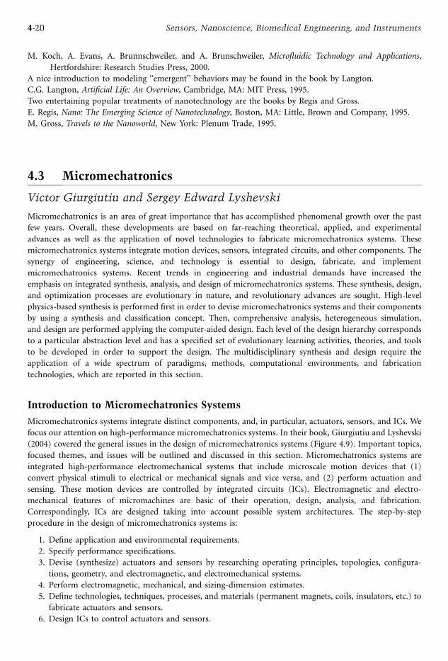
M. Koch, A. Evans, A. Brunnschweiler, and A. Brunschweiler, Microfluidic Technology and Applications,
Hertfordshire: Research Studies Press, 2000.
A nice introduction to modeling ‘‘emergent’’ behaviors may be found in the book by Langton.
C.G. Langton, Artificial Life: An Overview, Cambridge, MA: MIT Press, 1995.
Two entertaining popular treatments of nanotechnology are the books by Regis and Gross.
E. Regis, Nano: The Emerging Science of Nanotechnology, Boston, MA: Little, Brown and Company, 1995.
M. Gross, Travels to the Nanoworld, New York: Plenum Trade, 1995.
4.3 Micromechatronics
Victor Giurgiutiu and Sergey Edward Lyshevski
Micromechatronics is an area of great importance that has accomplished phenomenal growth over the past
few years. Overall, these developments are based on far-reaching theoretical, applied, and experimental
advances as well as the application of novel technologies to fabricate micromechatronics systems. These
micromechatronics systems integrate motion devices, sensors, integrated circuits, and other components. The
synergy of engineering, science, and technology is essential to design, fabricate, and implement
micromechatronics systems. Recent trends in engineering and industrial demands have increased the
emphasis on integrated synthesis, analysis, and design of micromechatronics systems. These synthesis, design,
and optimization processes are evolutionary in nature, and revolutionary advances are sought. High-level
physics-based synthesis is performed first in order to devise micromechatronics systems and their components
by using a synthesis and classification concept. Then, comprehensive analysis, heterogeneous simulation,
and design are performed applying the computer-aided design. Each level of the design hierarchy corresponds
to a particular abstraction level and has a specified set of evolutionary learning activities, theories, and tools
to be developed in order to support the design. The multidisciplinary synthesis and design require the
application of a wide spectrum of paradigms, methods, computational environments, and fabrication
technologies, which are reported in this section.
Introduction to Micromechatronics Systems
Micromechatronics systems integrate distinct components, and, in particular, actuators, sensors, and ICs. We
focus our attention on high-performance micromechatronics systems. In their book, Giurgiutiu and Lyshevski
(2004) covered the general issues in the design of micromechatronics systems (Figure 4.9). Important topics,
focused themes, and issues will be outlined and discussed in this section. Micromechatronics systems are
integrated high-performance electromechanical systems that include microscale motion devices that (1)
convert physical stimuli to electrical or mechanical signals and vice versa, and (2) perform actuation and
sensing. These motion devices are controlled by integrated circuits (ICs). Electromagnetic and electro-
mechanical features of micromachines are basic of their operation, design, analysis, and fabrication.
Correspondingly, ICs are designed taking into account possible system architectures. The step-by-step
procedure in the design of micromechatronics systems is:
1. Define application and environmental requirements.
2. Specify performance specifications.
3. Devise (synthesize) actuators and sensors by researching operating principles, topologies, configura-
tions, geometry, and electromagnetic, and electromechanical systems.
4. Perform electromagnetic, mechanical, and sizing-dimension estimates.
5. Define technologies, techniques, processes, and materials (permanent magnets, coils, insulators, etc.) to
fabricate actuators and sensors.
6. Design ICs to control actuators and sensors.
4-20 Sensors, Nanoscience, Biomedical Engineering, and Instruments

7. Develop high-fidelity mathematical models with a minimum level of simplifications and assumptions to
examine integrated electromagnetic, mechanical, vibroacoustic phenomena and effects.
8. Based upon data-intensive analysis and heterogeneous simulations, perform thorough electromagnetic,
mechanical, thermodynamic, and vibroacoustic design with performance analysis and outcome
prediction.
9. Modify and refine the design to optimize machine performance.
10. Design control laws to control micromechatronics systems and implement these controllers using ICs
(this task itself can be broken down to many subtasks and problems related to control laws design,
optimization, analysis, simulation, synthesis of ICs topologies, ICs fabrication, machine–ICs integration,
interfacing, and communication).
Before being engaged in the fabrication, one must solve synthesis, design, analysis, and optimization
problems. In fact, mechatronic systems’ performance and its suitability/applicability directly depend upon
synthesized topologies, configurations, and operating principles. The synthesis with modeling activities allows
the designer to examine complex phenomena, and discover advanced functionality and new operating
concepts. These guarantee synthesis of superior mechatronic systems with enhanced integrity, functionality,
and operationability. Thus, through the synthesis, the designer devises machines that must be modeled,
analyzed, simulated, and optimized. Finally, as shown in Figure 4.10, the devised and analyzed nano- and
micromachines must be fabricated and tested.
FIGURE 4.9 Micromechatronics: Modeling, Analysis, and Design with MATLAB, CRC Press, 2004.
SynthesisOptimization
Control
High-FidelityModeling
SimulationAnalysis
MicromechatronicSystem
FabricationTesting
Validation
FIGURE 4.10 Synthesis design and fabrication of micromechatronics systems.
4-21Materials and Nanoscience
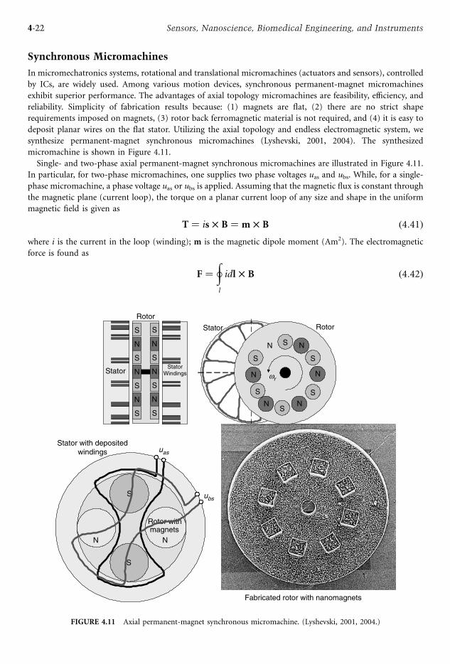
Synchronous Micromachines
In micromechatronics systems, rotational and translational micromachines (actuators and sensors), controlled
by ICs, are widely used. Among various motion devices, synchronous permanent-magnet micromachines
exhibit superior performance. The advantages of axial topology micromachines are feasibility, efficiency, and
reliability. Simplicity of fabrication results because: (1) magnets are flat, (2) there are no strict shape
requirements imposed on magnets, (3) rotor back ferromagnetic material is not required, and (4) it is easy to
deposit planar wires on the flat stator. Utilizing the axial topology and endless electromagnetic system, we
synthesize permanent-magnet synchronous micromachines (Lyshevski, 2001, 2004). The synthesized
micromachine is shown in Figure 4.11.
Single- and two-phase axial permanent-magnet synchronous micromachines are illustrated in Figure 4.11.
In particular, for two-phase micromachines, one supplies two phase voltages uas and ubs. While, for a single-
phase micromachine, a phase voltage uas or ubs is applied. Assuming that the magnetic flux is constant through
the magnetic plane (current loop), the torque on a planar current loop of any size and shape in the uniform
magnetic field is given as
T ¼ is B ¼ m B ð4:41Þwhere i is the current in the loop (winding); m is the magnetic dipole moment (Am2). The electromagnetic
force is found as
F ¼Il
idl B ð4:42Þ
Stator
Stator Rotor
StatorWindings
r
N
N
S
S
S
NS
S
S
N
N
NN
N
S
S
N
S
S
N
N
S
S
N
S
S
Rotor
S
N
S
N
ubs
uas
Rotor withmagnets
Fabricated rotor with nanomagnets
w
Stator with depositedwindings
FIGURE 4.11 Axial permanent-magnet synchronous micromachine. (Lyshevski, 2001, 2004.)
4-22 Sensors, Nanoscience, Biomedical Engineering, and Instruments
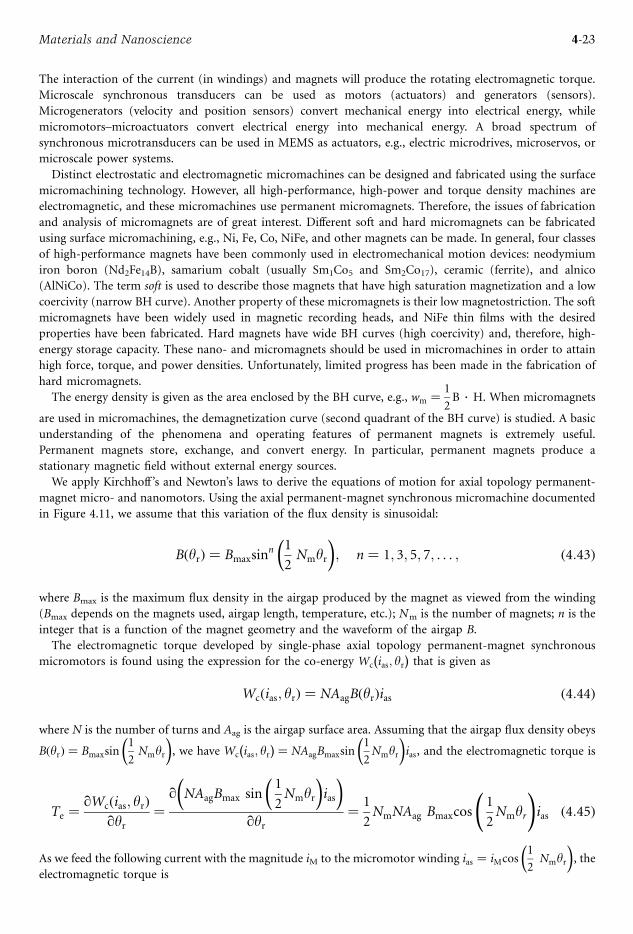
The interaction of the current (in windings) and magnets will produce the rotating electromagnetic torque.
Microscale synchronous transducers can be used as motors (actuators) and generators (sensors).
Microgenerators (velocity and position sensors) convert mechanical energy into electrical energy, while
micromotors–microactuators convert electrical energy into mechanical energy. A broad spectrum of
synchronous microtransducers can be used in MEMS as actuators, e.g., electric microdrives, microservos, or
microscale power systems.
Distinct electrostatic and electromagnetic micromachines can be designed and fabricated using the surface
micromachining technology. However, all high-performance, high-power and torque density machines are
electromagnetic, and these micromachines use permanent micromagnets. Therefore, the issues of fabrication
and analysis of micromagnets are of great interest. Different soft and hard micromagnets can be fabricated
using surface micromachining, e.g., Ni, Fe, Co, NiFe, and other magnets can be made. In general, four classes
of high-performance magnets have been commonly used in electromechanical motion devices: neodymium
iron boron (Nd2Fe14B), samarium cobalt (usually Sm1Co5 and Sm2Co17), ceramic (ferrite), and alnico
(AlNiCo). The term soft is used to describe those magnets that have high saturation magnetization and a low
coercivity (narrow BH curve). Another property of these micromagnets is their low magnetostriction. The soft
micromagnets have been widely used in magnetic recording heads, and NiFe thin films with the desired
properties have been fabricated. Hard magnets have wide BH curves (high coercivity) and, therefore, high-
energy storage capacity. These nano- and micromagnets should be used in micromachines in order to attain
high force, torque, and power densities. Unfortunately, limited progress has been made in the fabrication of
hard micromagnets.
The energy density is given as the area enclosed by the BH curve, e.g., wm ¼ 1
2B H. When micromagnets
are used in micromachines, the demagnetization curve (second quadrant of the BH curve) is studied. A basic
understanding of the phenomena and operating features of permanent magnets is extremely useful.
Permanent magnets store, exchange, and convert energy. In particular, permanent magnets produce a
stationary magnetic field without external energy sources.
We apply Kirchhoff ’s and Newton’s laws to derive the equations of motion for axial topology permanent-
magnet micro- and nanomotors. Using the axial permanent-magnet synchronous micromachine documented
in Figure 4.11, we assume that this variation of the flux density is sinusoidal:
BðyrÞ ¼ Bmaxsinn 1
2Nmyr ; n ¼ 1; 3; 5; 7; . . . ; ð4:43Þ
where Bmax is the maximum flux density in the airgap produced by the magnet as viewed from the winding
(Bmax depends on the magnets used, airgap length, temperature, etc.); Nm is the number of magnets; n is the
integer that is a function of the magnet geometry and the waveform of the airgap B.
The electromagnetic torque developed by single-phase axial topology permanent-magnet synchronous
micromotors is found using the expression for the co-energy Wc ias; yr that is given as
Wcðias; yrÞ ¼ NAagBðyrÞias ð4:44Þ
where N is the number of turns and Aag is the airgap surface area. Assuming that the airgap flux density obeys
BðyrÞ ¼ Bmaxsin1
2Nmyr , we have Wc ias; yr ¼ NAagBmaxsin
1
2Nmyr ias, and the electromagnetic torque is
Te ¼ qWcðias; yrÞqyr
¼q NAagBmax sin
1
2Nmyr ias
qyr¼ 1
2NmNAag Bmaxcos
1
2Nmyr
!ias ð4:45Þ
As we feed the following current with the magnitude iM to the micromotor winding ias ¼ iMcos1
2Nmyr , the
electromagnetic torque is
4-23Materials and Nanoscience

Te ¼ 1
2NmNAagBmaxiMcos
2 1
2Nmyr
!6¼ 0 ð4:46Þ
The mathematical model of the single-phase permanent-magnet micromotor is found by using Kirchhoff ’s
and Newton’s second laws:
uas ¼ rsias þ dcas
dtðcircuitry equationÞ ð4:47Þ
Te Bmor TL ¼ Jd2yrdt2
ðtorsional mechanical equationÞ ð4:48Þ
From the flux linkage equation cas ¼ Lasias þ NAagBðyrÞ, we have
dcasdt
¼ Lasdiasdt
þ NAagdBðyrÞdt
¼ Lasdiasdt
þ 12 NmNAag Bmax cos
1
2Nmyr or ð4:49Þ
Thus, a set of three first-order nonlinear differential equations results, which models a single-phase axial
topology permanent-magnet synchronous micromotors. In particular:
diasdt
¼ 1
Lasrsias
1
2NmNAag Bmax cos
1
2Nmyr or þ uas ð4:50Þ
dor
dt¼ 1
J
1
2NmNAag Bmax cos
1
2Nmyr
!ias Bmor TL
!ð4:51Þ
dyrdt
¼ or ð4:52Þ
Single-phase axial permanent-magnet synchronous micro- and nanomachines may have a torque ripple. To
avoid this torque ripple, one must design two-phase machines. For two-phase machines, the co-energy and
electromagnetic torque are given as
Wc ias; yr ¼ NAagBmax sin1
2Nmyr
!ias cos
1
2Nmyr
!ibs
!ð4:53Þ
and the electromagnetic torque is
Te ¼ qWcðias; yrÞqyr
¼ 1
2NmNAagBmax cos
1
2Nmyr
!ias þ sin
1
2Nmyr
!ibs
!ð4:54Þ
Thus, feeding the phase currents as
ias ¼ iMcos1
2Nmyr and ibs ¼ iMsin
1
2Nmyr ð4:55Þ
4-24 Sensors, Nanoscience, Biomedical Engineering, and Instruments

we obtain
Te ¼ 1
2NmNAagBmaxiM cos2
1
2Nmyr
!þ sin2
1
2NmyrÞ
!¼ 1
2NmNAagBmaxiM ð4:56Þ
The model developments and control issues are reported in Lyshevski (2001).
Fabrication Aspects
Micromachines can be fabricated through deposition of the conductors (coils and windings), ferromagnetic
core, magnets, insulating layers, as well as other microstructures (movable and stationary members and their
components including bearings). The subsequent order of the processes, sequential steps, and materials are
different depending on the machines devised, designed, analyzed, and optimized. Several textbooks (Madou,
1997; Kovacs, 1998; Lyshevski, 2001, 2004; Giurgiutiu and Lyshevski, 2004) provide the reader with the basic
fabrication features and processes involved in the micromachine fabrication. This section outlines the most
viable aspects.
Complementary metal oxide semiconductor (CMOS), high-aspect-ratio (LIGA and LIGA-like), and surface
micromachining technologies are key features for fabrication of nano- and micromachines and structures. The
LIGA (Lithography–Galvanoforming–Molding, or, in German, Lithografie–Galvanik–Abformung) technology
allows one to make three-dimensional microstructures with the aspect ratio (depth vs. lateral dimension is
more than 100). The LIGA technology is based on x-ray lithography, which ensures short wavelength (from
few to 10 A) which leads to negligible diffraction effects and larger depth of focus compared with photo-
lithography. The major processes in the machines’ microfabrication are diffusion, deposition, patterning,
lithography, etching, metallization, planarization, assembling, and packaging. Thin-film fabrication processes
were developed and used for polysilicon, silicon dioxide, silicon nitride, and other different materials, e.g.,
metals, alloys, and composites. The basic steps are: lithography, deposition of thin films and materials
(electroplating, chemical vapor deposition, plasma enhanced chemical vapor deposition, evaporation,
sputtering, spraying, screen printing), removal of material (patterning) by wet or dry techniques, etching
(plasma etching, reactive ion etching, laser etching, etc.), doping, bonding (fusion, anodic, and other), and
planarization (Madou, 1997; Kovacs, 1998; Lyshevski, 2001, 2004).
To fabricate motion and radiating energy nano- and microscale structures and devices, different fabrication
technologies are used (Madou, 1997; Kovacs, 1998; Lyshevski, 2001, 2004). New processes were developed and
novel materials were applied to modify the CMOS, surface micromachining, and LIGA technologies.
Currently, the state of the art in nanofabrication has progressed to nanocircuits and nanodevices (Lyshevski,
2004). Nano- and micromachines and their components (stator, rotor, bearing, coils, etc.) are defined
photographically, and the high-resolution photolithography is applied to define two- (planar) and three-
dimensional shapes (geometry). Deep ultraviolet lithography processes were developed to decrease the feature
sizes of microstructures to 0.1 mm. Different exposure wavelengths l (435, 365, 248, 200, 150, or 100 nm) areused. Using the Rayleigh model for image resolution, the expressions for image resolution iR and the depth of
focus dF are given by
iR ¼ kilNA
; dF ¼ kdlN2A
ð4:57Þ
where ki and kd are the lithographic process constants; l is the exposure wavelength; NA is the numerical
aperture coefficient (for high-numerical aperture we have NA ¼ 0.5 to 0.6).
The g- and i-line IBM lithography processes (with wavelengths of 435 and 365 nm, respectively) allow
one to attain 0.35-mm features. The deep ultraviolet light sources (mercury source or excimer lasers) with
248-nm wavelength enables the industry to achieve 0.25-mm resolution. The changes to short exposure
wavelength possess challenges and present new highly desired possibilities. However, using CMOS technology,
4-25Materials and Nanoscience

50-nm features were achieved, and the application of x-ray lithography led to nanometer scale features
(Madou, 1997; Kovacs, 1998; Lyshevski, 2001, 2004). Different lithography processes commonly applied are:
photolithography, screen printing, electron-beam lithography, and x-ray lithography (high-aspect ratio
technology).
Although machine topologies and configurations vary, magnetic and insulating materials, magnets, and
windings are used in all motion devices. Figure 4.12 illustrates the electroplated 10-mm wide and thick with
10-mm spaced insulated copper microwindings (deposited on ferromagnetic cores), microstructures, and
permanent magnets (electroplated NiFe alloy) as shown by Lyshevski (2001).
Electroactive and Magnetoactive Materials
Electroactive and magnetoactive materials are the building blocks of micromechatronics. The intrinsic active
behavior of these materials, which change dimensions in response to electric and magnetic fields, make them
ideal for actuation and sensing at the micro level.
Electroactive Materials
Electroactive materials can be divided into piezoelectric and electrostrictive. Linear piezoelectric materials obey
the constitutive relations between the mechanical and electrical variables, which can be written in tensor
notations as
Sij ¼ sEijklTkl þ dijkEk þ dijaEi y ð4:58Þ
Dj ¼ djklTkl þ eTjkEk þ ~DDjy ð4:59Þwhere Sij is the mechanical strain, Tkl the mechanical stress, Ek the electrical field, and Dj the electrical
displacement. The variable sEijkl is themechanical complianceof thematerialmeasured at zero electric field (E¼0),
eTjk is the dielectric permittivity measured at zero mechanical stress (T¼ 0), and dkij is the piezoelectric coupling
between the electrical and mechanical variables. The variable y is the temperature, and aEi is the coefficient ofthermal expansion under constant electric field. The coefficient ~DDj is the electric displacement temp-
erature coefficient. The stress and strain variables are second-order tensors, while the electric field and the electric
displacement are first-order tensors. Since thermal effects only influence the diagonal terms, the respective
coefficients, ai and ~DDj, have single subscripts. The term dij is the Kroneker delta (dij ¼ 1 if i ¼ j; zero otherwise).
The physical explanation of the piezoelectric effect is represented schematically in Figure 4.13a.
Electromechanical coupling coefficient is the square root of the ratio between the mechanical energy stored
and the electrical energy applied to a piezoelectric material, i.e.:
k ¼ffiffiffiffiffiffiffiffiffiffiffiffiffiffiffiffiffiffiffiffiffiffiffiffiffiffiffiffiffiffiffimechanical energy stored
electrical energy applied
sð4:60Þ
FIGURE 4.12 Deposited copper microwindings, microstructure, and permanent magnets.
4-26 Sensors, Nanoscience, Biomedical Engineering, and Instruments

For direct actuation, k33 ¼ d33=ffiffiffiffiffiffiffis33e33
p, where Voigt matrix notations are used. For transverse actuation,
k31 ¼ d31=ffiffiffiffiffiffiffis11e33
p; for shear actuation, k15 ¼ d15=
ffiffiffiffiffiffiffis55e11
p. For uniform inplane actuation, we obtain the planar
coupling coefficient, kp ¼ k13ffiffiffiffiffiffiffiffiffiffiffi2=ð1 nÞp
, where n is the Poisson ratio. The piezoelectric response in axial andshear directions is depicted in Figure 4.14.
In contrast with linear piezoelectricity, the electrostrictive response is quadratic in electric field. Hence, the
direction of electrostriction does not change as the polarity of the electric field is reversed. The general
constitutive equations incorporate both piezoelectric and electrostrictive terms:
Sij ¼ sEklijTkl þ dkijEk þMklijEkEl ð4:61Þ
Dm ¼ dmklTkl þ eTmnEn þ 2MmnijEnTij ð4:62Þ
Note that the first two terms in each equation signify the linear piezoelectric behavior. The third term
represents the nonlinear electrostrictive behavior. The coefficients Mklij are the electrostrictive coefficients.
Magnetoactive Materials
Most magnetoactive materials are based on the magnetostrictive effect. The magnetostrictive constitutive
equations contain both linear and quadratic terms:
Sij ¼ sEijklTkl þ dkijHk þMklijHkHl ð4:63ÞBm ¼ dmklTkl þ mTmkHk þ 2MmnijEnTij ð4:64Þ
where, in addition to the already defined variables, Hk is the magnetic field intensity, Bj is the magnetic flux
density, and mTjk is the magnetic permeability under constant stress. The coefficients dkij andMklij are defined in
terms of magnetic units. The magnetic field intensity in a rod surrounded by a coil with n turns per unit length
depends on the coil current, I :
H ¼ nI ð4:65Þ
(a)
V+
−PS−
+
l − ∆l
t +∆t
(b)
V+
− − +
l
tPS
FIGURE 4.14 Induce-strain responses of piezoelectric materials: (a) axial strain; (b) shear strain.
(a)
PS
(–)
(+)
(b)
+
+
+
+
m-e
FIGURE 4.13 Physical explanation of induced-strain actuation: (a) piezoelectric response in a perovskite structure;
(b) magetostrictive lattice deformation due to the rotation of the inner-shell charge-density oblate shape in a magnetic field.
4-27Materials and Nanoscience
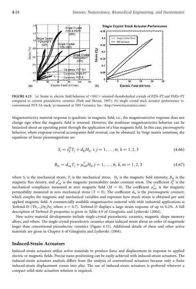
Magnetostrictive material response is quadratic in magnetic field, i.e., the magnetostrictive response does not
change sign when the magnetic field is reversed. However, the nonlinear magnetostrictive behavior can be
linearized about an operating point through the application of a bias magnetic field. In this case, piezomagnetic
behavior, where response-reversal accompanies field reversal, can be obtained. In Voigt matrix notations, the
equations of linear piezomagnetism are
Si ¼ sHij Tj þ dkiHk; i; j ¼ 1; . . . ; 6; k ¼ 1; 2; 3 ð4:66Þ
Bm ¼ dmjTj þ mTmkHk; j ¼ 1; . . . ; 6; k;m ¼ 1; 2; 3 ð4:67Þ
where Si is the mechanical strain, Tj is the mechanical stress, Hk is the magnetic field intensity, Bm is the
magnetic flux density, and mTmk is the magnetic permeability under constant stress. The coefficient sHij is the
mechanical compliance measured at zero magnetic field (M ¼ 0). The coefficient mTmk is the magnetic
permeability measured at zero mechanical stress (T ¼ 0). The coefficient dki is the piezomagnetic constant,
which couples the magnetic and mechanical variables and expresses how much strain is obtained per unit
applied magnetic field. A commercially available magnetoactive material with wide industrial applications is
Terfenol-D (Tb1 xDyxFe2 where x ¼ 0.7). Terfenol-D displays a large strain response of up to 0.2%. A full
description of Terfenol-D properties is given in Table 4.9 of Giurgiutiu and Lyshevski (2004).
New active material developments include single-crystal piezoelectric ceramics, magnetic shape memory
alloys, and others. The single crystal piezoelectric ceramics attain induced strain about an order of magnitude
larger than conventional piezoelectric ceramics (Figure 4.15). Additional details of these and other active
materials are given in Chapter 4 of Giurgiutiu and Lyshevski (2004).
Induced-Strain Actuators
Induced-strain actuators utilize active materials to produce force and displacement in response to applied
electric or magnetic fields. Precise nano-positioning can be easily achieved with induced-strain actuators. The
induced-strain actuators analysis differs from the analysis of conventional actuators because only a finite
induced-strain displacement comes into play. The use of induced-strain actuators is preferred wherever a
compact solid-state actuation solution is required.
FIGURE 4.15 (a) Strain vs. electric field behavior of ,001. oriented rhombohedral crystals of PZN–PT and PMN–PT
compared to current piezoelectric ceramics (Park and Shrout, 1997); (b) single crystal stack actuator performance vs.
conventional PZT-5A stack, as measured at TRS Ceramics, Inc. (http://www.trsceramics.com).
4-28 Sensors, Nanoscience, Biomedical Engineering, and Instruments

Linearized Electromechanical Behavior of Induced-Strain Actuators
Induced-strain actuator vendor data usually contains the free-stroke, uISA, the corresponding maximum
voltage, V, the internal stiffness, ki, and the capacitance, C. Based on vendor data, one can calculate the
apparent elastic compliance, s, electrical permittivity, e, and piezoelectric strain coefficient, d, for full-strokeoperation. For a piezoelectric stack:
s ¼ A
lkiðapparent zero field elastic complianceÞ ð4:68Þ
e ¼ C
A
t2
lðapparent zero stress electrical permittivityÞ ð4:69Þ
d ¼ uISAV
t
lðapparent piezoelectric strain coefficientÞ ð4:70Þ
where l, A, and ki are the length, cross-sectional area, and internal stiffness, while t is the piezo layer thickness.
The effective full-stroke electromechanical coupling coefficient of the piezoelectric stack actuator is obtained as
k2 ¼ d2
se¼ kiu
2ISA
CV2 ð4:71Þ
For magnetoactive actuators, a similar process is employed using current, I, and inductance, L, instead of
voltage, V, and capacitance, C. As a result, the effective full-stroke electromechanical coupling coefficient of the
magnetoactive actuator is obtained as
k2 ¼ d2
sm¼ kiu
2ISA
LI2ð4:72Þ
The behavior of a typical piezoelectric induced-strain actuator under static and dynamic operation is given in
Figure 4.16. Similar results for electrostrictive and magnetostrictive actuators can be found in Giurgiutiu and
Lyshevski (2004) (Figure 4.19 and Figure 4.20).
u
−200
0
20
40
60
80
100
120
−200 0 200 400 600 800 1000
−V, Volts
u(V
),μm
u+ISA
u−ISA
ustaticISA
udynamicISA
udynamicISA
Polytec PlType P-245.70May 9. 1996
FIGURE 4.16 Induced-strain displacement vs. applied voltage for Polytec PI model P-245.70 piezoelectric (PZT) actuator.
4-29Materials and Nanoscience
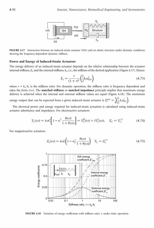
Power and Energy of Induced-Strain Actuators
The energy delivery of an induced-strain actuator depends on the relative relationship between the actuator
internal stiffness, ki, and the external stiffness, ke, i.e., the stiffness of the desired application (Figure 4.17). Hence:
Ee ¼ r
1þ rð Þ21
2kiu
2ISA ð4:73Þ
where r ¼ ke=ki is the stiffness ratio. For dynamic operation, the stiffness ratio is frequency dependent and
takes the form r(o). The matched stiffness or matched impedance principle implies that maximum energy
delivery is achieved when the internal and external stiffness values are equal (Figure 4.18). The maximum
energy output that can be expected from a given induced-strain actuator is Emaxe ¼ 1
4
1
2kiu
2ISA .
The electrical power and energy required for induced-strain actuation is calculated using induced-strain
actuator admittance and impedance. For electroactive actuators:
YCðoÞ ¼ ioC 1 k2rrðoÞ
1þ rrðoÞ ¼ YRC ðoÞ þ iY ICðoÞ; ZC ¼ Y 1C ð4:74Þ
For magnetoactive actuators:
ZLðoÞ ¼ ioL 1 k2LrrðoÞ
1þ rrðoÞ YL ¼ Z 1L ð4:75Þ
0
0.25
0.5
0.75
1
0.01 0.1 1 10 100
Ene
rgy
coef
ficie
nts
ISA energycoefficient,E’ISA
Internal energycoefficient,E’ i
Stiffness ratio, r = ke/ki
kekiuISA
External energycoefficient,E’e
FIGURE 4.18 Variation of energy coefficients with stiffness ratio, r, under static operation.
u(t)
ce
F(t)
ke
StructuremeISAv(t)
i(t)
FIGURE 4.17 Interaction between an induced-strain actuator (ISA) and an elastic structure under dynamic conditions
showing the frequency-dependent dynamic stiffness.
4-30 Sensors, Nanoscience, Biomedical Engineering, and Instruments
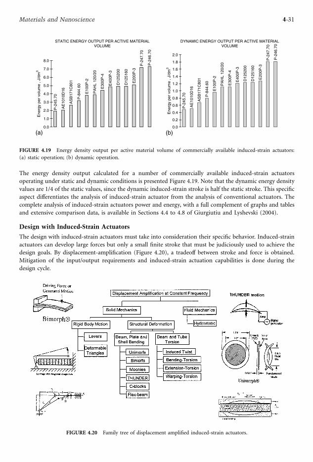
The energy density output calculated for a number of commercially available induced-strain actuators
operating under static and dynamic conditions is presented Figure 4.19. Note that the dynamic energy density
values are 1/4 of the static values, since the dynamic induced-strain stroke is half the static stroke. This specific
aspect differentiates the analysis of induced-strain actuator from the analysis of conventional actuators. The
complete analysis of induced-strain actuators power and energy, with a full complement of graphs and tables
and extensive comparison data, is available in Sections 4.4 to 4.8 of Giurgiutiu and Lyshevski (2004).
Design with Induced-Strain Actuators
The design with induced-strain actuators must take into consideration their specific behavior. Induced-strain
actuators can develop large forces but only a small finite stroke that must be judiciously used to achieve the
design goals. By displacement-amplification (Figure 4.20), a tradeoff between stroke and force is obtained.
Mitigation of the input/output requirements and induced-strain actuation capabilities is done during the
design cycle.
STATIC ENERGY OUTPUT PER ACTIVE MATERIALVOLUME
P-2
45.7
0
AE
1010
D16
AS
B17
1C80
1
P-8
44.6
0
E10
0P-2
PA
HL
120/
20
E30
0P-4
E40
0P-3
D12
5200
D12
5160
E20
0P-3
P-2
47.7
0
P-2
46.7
0
0.0
1.0
2.0
3.0
4.0
5.0
6.0
7.0
8.0
Ene
rgy
per
volu
me
,J/d
m3
(b)
DYNAMIC ENERGY OUTPUT PER ACTIVE MATERIALVOLUME
P-2
45.7
0
AE
1010
D16
AS
B17
1C80
1
P-8
44.6
0
E10
0P-2
PA
HL
120/
20
E30
0P-4
E40
0P-3
D12
5200
D12
5160
E20
0P-3
P-2
47.7
0
P-2
46.7
0
0.0
0.2
0.4
0.6
0.8
1.0
1.2
1.4
1.6
1.8
2.0
Ene
rgy
per
volu
me
,J/d
m3
(a)
FIGURE 4.19 Energy density output per active material volume of commercially available induced-strain actuators:
(a) static operation; (b) dynamic operation.
FIGURE 4.20 Family tree of displacement amplified induced-strain actuators.
4-31Materials and Nanoscience

Piezoelectric Wafer Active Sensors
Piezoelectric wafer active sensors (PWAS) are small and unobtrusive active-material devices that can act at
both transmitters and receivers of elastic waves traveling in various materials (Figure 4.21). PWAS are the
enabling technology for many micromechatronics applications, such as embedded sensing, vibration control,
and structural health monitoring of cracks and defects.
PWAS Resonators
The analysis of PWAS resonators starts with the 1D analysis of rectangular PWAS and then extends to the 2D
axisymmetric analysis of circular PWAS.
Rectangular PWAS Resonators
The 1D analysis of rectangular PWAS assumes that the ratio between length, width, and thickness is such that
the respective vibrations can be considered uncoupled (Figure 4.22). Direct use of the constitutive Equation
(4.58) yields the 1D wave equation:
€uu1 ¼ c2u001 ð4:76Þ
where c2 ¼ 1=rsE11 is the wave speed. For ac excitation, E3 ¼ EE3eiot , the solution is
uu1ðxÞ ¼ d31EE3g
sin gx
cos1
2gl
ð4:77Þ
FIGURE 4.21 Piezoelectric wafer active sensors (PWAS) mounted on an aircraft panel.
(a)
(b)
x3
x1, u1
Electric field, E3
PZT active sensor
length l, thickness h; width, b. (c)
1u
T 1 + dT 1T 1
Poling direction
b
l
h
x3
x1
x2
FIGURE 4.22 Schematic of a piezoelectric active sensor and infinitesimal axial element.
4-32 Sensors, Nanoscience, Biomedical Engineering, and Instruments
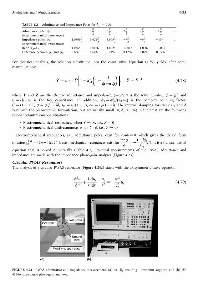
For electrical analysis, the solution substituted into the constitutive Equation (4.59) yields, after some
manipulations:
YY ¼ io CC 1 kk231 11
jj cotjj; ZZ ¼ YY 1 ð4:78Þ
where YY and ZZ are the electric admittance and impedance, g¼o/c g is the wave number, f ¼ 12gl, and
C ¼ eT33bl=h is the free capacitance. In addition, kk213 ¼ d231= ss11ee33 is the complex coupling factor,
CC ¼ 1 ieð ÞC, jj ¼ jffiffiffiffiffiffiffi1 id
p, ss11 ¼ s11ð1 iZÞ, ee33 ¼ e33 1 idð Þ. The internal damping loss values Z and d
vary with the piezoceramic formulation, but are usually small (Z, d, . 5%). Of interest are the following
resonance/antiresonance situations:
. Electromechanical resonance, when Y ! 1, i.e., Z ¼ 0
. Electromechanical antiresonance, when Y¼0, i.e., Z ! 1Electromechanical resonances, i.e., admittance poles, exist for cosf ¼ 0, which gives the closed form
solution f EMn ¼ 2n 1ð Þc=2l. Electromechanical resonances exist for tanff
¼ 1 k231k231
. This is a transcendental
equation that is solved numerically (Table 4.2). Practical measurements of the PWAS admittance and
impedance are made with the impedance phase-gain analyzer (Figure 4.23).
Circular PWAS Resonators
The analysis of a circular PWAS resonator (Figure 4.24a) starts with the axisymmetric wave equation:
d2urdr2
þ 1
r
durdr
urr2¼ o2
c2pur ð4:79Þ
TABLE 4.2 Admittance and Impedance Poles for k31 ¼ 0:36
Admittance poles, fY
(electromechanical resonances)
3p2
5p2
7p2
9p2
11p2
. . .
Impedance poles, fZ
(electromechanical resonances)
1.0565p2
3.021p2
5.005p2
7p2
9p2
11p2
. . .
Ratio fZ /fY 1.0565 1.0066 1.0024 1.0012 1.0007 1.0005 . . .
Difference between fZ and fY 5.6% 0.66% 0.24% 0.12% 0.07% 0.05%
FIGURE 4.23 PWAS admittance and impedance measurement: (a) test jig ensuring unrestraint support, and (b) HP
4194A impedance phase-gain analyzer.
4-33Materials and Nanoscience
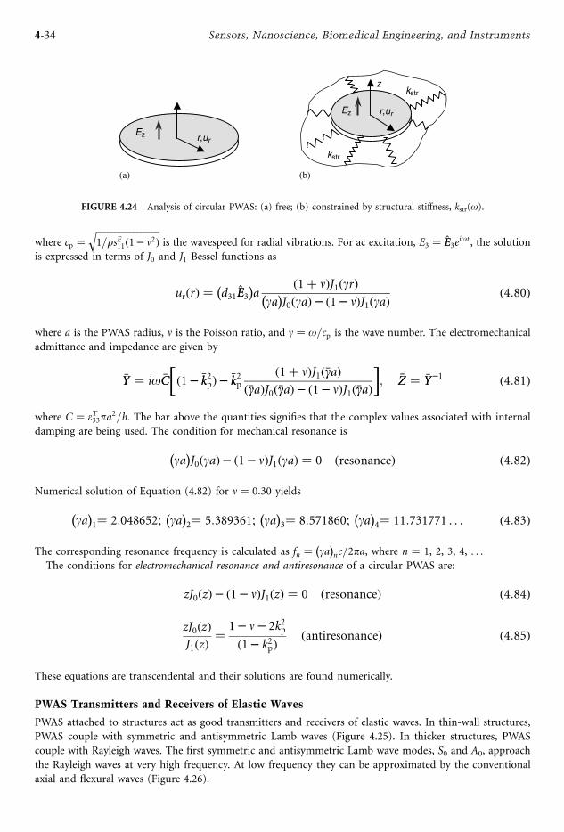
where cp ¼ffiffiffiffiffiffiffiffiffiffiffiffiffiffiffiffiffi1=rsE11ð1 n2Þ
qis the wavespeed for radial vibrations. For ac excitation, E3 ¼ EE3e
iot , the solution
is expressed in terms of J0 and J1 Bessel functions as
urðrÞ ¼ d31EE3 a1þ nð ÞJ1ðgrÞ
ga J0ðgaÞ 1 nð ÞJ1ðgaÞ ð4:80Þ
where a is the PWAS radius, n is the Poisson ratio, and g ¼ o=cp is the wave number. The electromechanicaladmittance and impedance are given by
YY ¼ ioCC ð1 kk2pÞ kk2pð1þ nÞJ1ðggaÞ
ðggaÞJ0ðggaÞ ð1 nÞJ1ðggaÞ ; ZZ ¼ YY 1 ð4:81Þ
where C ¼ eT33pa2=h. The bar above the quantities signifies that the complex values associated with internal
damping are being used. The condition for mechanical resonance is
ga J0ðgaÞ 1 nð ÞJ1ðgaÞ ¼ 0 ðresonanceÞ ð4:82Þ
Numerical solution of Equation (4.82) for n ¼ 0:30 yields
ga 1¼ 2:048652; ga 2¼ 5:389361; ga 3¼ 8:571860; ga 4¼ 11:731771 . . . ð4:83Þ
The corresponding resonance frequency is calculated as fn ¼ ga nc=2pa, where n ¼ 1, 2, 3, 4, . . .
The conditions for electromechanical resonance and antiresonance of a circular PWAS are:
zJ0ðzÞ 1 nð ÞJ1ðzÞ ¼ 0 ðresonanceÞ ð4:84Þ
zJ0ðzÞJ1ðzÞ ¼
1 n 2k2pð1 k2pÞ ðantiresonanceÞ ð4:85Þ
These equations are transcendental and their solutions are found numerically.
PWAS Transmitters and Receivers of Elastic Waves
PWAS attached to structures act as good transmitters and receivers of elastic waves. In thin-wall structures,
PWAS couple with symmetric and antisymmetric Lamb waves (Figure 4.25). In thicker structures, PWAS
couple with Rayleigh waves. The first symmetric and antisymmetric Lamb wave modes, S0 and A0, approach
the Rayleigh waves at very high frequency. At low frequency they can be approximated by the conventional
axial and flexural waves (Figure 4.26).
(a) (b)
zkstr
kstr
r,ur
r,ur
Ez
Ez
FIGURE 4.24 Analysis of circular PWAS: (a) free; (b) constrained by structural stiffness, kstr(o).
4-34 Sensors, Nanoscience, Biomedical Engineering, and Instruments
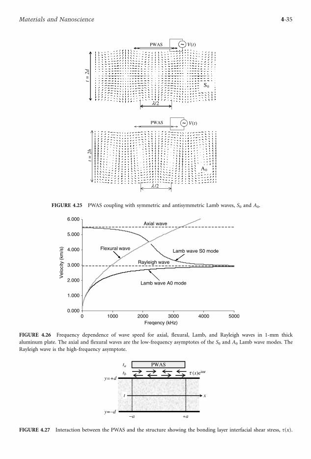
t=2d
λ/2
PWAS ~ V(t)
S0
λ /2
t=2h
PWAS ~ V(t)
A0
FIGURE 4.25 PWAS coupling with symmetric and antisymmetric Lamb waves, S0 and A0.
0.000
1.000
2.000
3.000
4.000
5.000
6.000
0 1000 2000 3000 4000 5000Freqency (kHz)
Vel
ocity
(km
/s)
Axial wave
Lamb wave A0 mode
Lamb wave S0 mode
Rayleigh wave
Flexural wave
FIGURE 4.26 Frequency dependence of wave speed for axial, flexural, Lamb, and Rayleigh waves in 1-mm thick
aluminum plate. The axial and flexural waves are the low-frequency asymptotes of the S0 and A0 Lamb wave modes. The
Rayleigh wave is the high-frequency asymptote.
PWAS
−a +a
x
t (x)eiωt
ta
t
tby=+d
y=−d
FIGURE 4.27 Interaction between the PWAS and the structure showing the bonding layer interfacial shear stress, t(x).
4-35Materials and Nanoscience
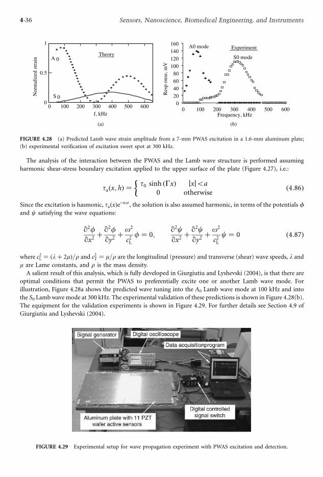
The analysis of the interaction between the PWAS and the Lamb wave structure is performed assuming
harmonic shear-stress boundary excitation applied to the upper surface of the plate (Figure 4.27), i.e.:
taðx; hÞ ¼ t0 sinh ðGxÞ jxj5a0 otherwise
ð4:86ÞSince the excitation is hasmonic, taðxÞe iot , the solution is also assumed harmonic, in terms of the potentials f
and c satisfying the wave equations:
q2fqx2
þ q2fqy2
þ o2
c2Lf ¼ 0;
q2cqx2
þ q2cqy2
þ o2
c2Lc ¼ 0 ð4:87Þ
where c2L ¼ ðlþ 2mÞ=r and c2T ¼ m=r are the longitudinal (pressure) and transverse (shear) wave speeds, l andm are Lame constants, and r is the mass density.A salient result of this analysis, which is fully developed in Giurgiutiu and Lyshevski (2004), is that there are
optimal conditions that permit the PWAS to preferentially excite one or another Lamb wave mode. For
illustration, Figure 4.28a shows the predicted wave tuning into the A0 Lamb wave mode at 100 kHz and into
the S0 Lambwavemode at 300 kHz. The experimental validation of these predictions is shown in Figure 4.28(b).
The equipment for the validation experiments is shown in Figure 4.29. For further details see Section 4.9 of
Giurgiutiu and Lyshevski (2004).
(a) (b)
0 100 200 300 400 500 6000
0.5
1
f, kHz
Nor
mal
ized
stra
in
S 0
A 0Theory
Res
pon
se,m
V
020406080
100120140160
0 100 200 300 400 500 600Frequency, kHz
S0 mode
A0 mode Experiment
FIGURE 4.28 (a) Predicted Lamb wave strain amplitude from a 7-mm PWAS excitation in a 1.6-mm aluminum plate;
(b) experimental verification of excitation sweet spot at 300 kHz.
FIGURE 4.29 Experimental setup for wave propagation experiment with PWAS excitation and detection.
4-36 Sensors, Nanoscience, Biomedical Engineering, and Instruments
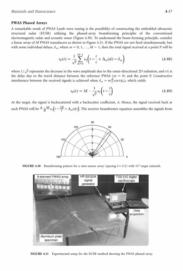
PWAS Phased Arrays
A remarkable result of PWAS Lamb wave tuning is the possibility of constructing the embedded ultrasonic
structural radar (EUSR) utilizing the phased-array beamforming principles of the conventional
electromagnetic radar and acoustic sonar (Figure 4.30). To understand the beam-forming principle, consider
a linear array of M PWAS transducers as shown in Figure 4.31. If the PWAS are not fired simultaneously, but
with some individual delays, dm, where m ¼ 0, 1, . . ., M 1, then the total signal received at a point P will be
sPðtÞ ¼ 1ffiffir
p XM 1
m¼0sT t
r
cþ DmðfÞ dm ð4:88Þ
where 1=ffiffir
prepresents the decrease in the wave amplitude due to the omni-directional 2D radiation, and r/c is
the delay due to the travel distance between the reference PWAS (m ¼ 0) and the point P. Constructive
interference between the received signals is achieved when dm ¼ mdc cos ðf0Þ, which yields
sPðtÞ ¼ M1ffiffir
p sT tr
cð4:89Þ
At the target, the signal is backscattered with a backscatter coefficient, A. Hence, the signal received back at
each PWAS will be A MR sT t 2R
c þ DmðfÞ . The receiver beamformer equation assembles the signals from
0
30
60
90
120
150
180
8
6
4
2
0
FIGURE 4.30 Beamforming pattern for a nine-sensor array (spacing I¼l/2) with 53 target azimuth.
FIGURE 4.31 Experimental setup for the EUSR method showing the PWAS phased array.
4-37Materials and Nanoscience
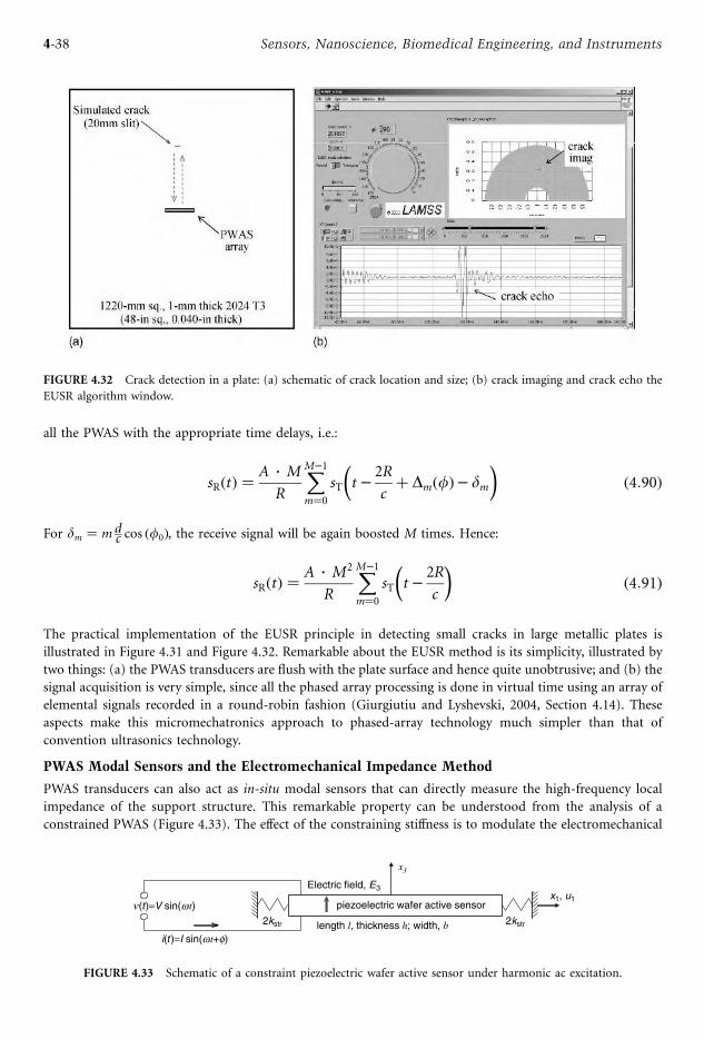
all the PWAS with the appropriate time delays, i.e.:
sRðtÞ ¼ A M
R
XM 1
m¼0sT t
2R
cþ DmðfÞ dm ð4:90Þ
For dm ¼ mdc cos ðf0Þ, the receive signal will be again boosted M times. Hence:
sRðtÞ ¼ A M2
R
XM 1
m¼0sT t
2R
cð4:91Þ
The practical implementation of the EUSR principle in detecting small cracks in large metallic plates is
illustrated in Figure 4.31 and Figure 4.32. Remarkable about the EUSR method is its simplicity, illustrated by
two things: (a) the PWAS transducers are flush with the plate surface and hence quite unobtrusive; and (b) the
signal acquisition is very simple, since all the phased array processing is done in virtual time using an array of
elemental signals recorded in a round-robin fashion (Giurgiutiu and Lyshevski, 2004, Section 4.14). These
aspects make this micromechatronics approach to phased-array technology much simpler than that of
convention ultrasonics technology.
PWAS Modal Sensors and the Electromechanical Impedance Method
PWAS transducers can also act as in-situ modal sensors that can directly measure the high-frequency local
impedance of the support structure. This remarkable property can be understood from the analysis of a
constrained PWAS (Figure 4.33). The effect of the constraining stiffness is to modulate the electromechanical
FIGURE 4.32 Crack detection in a plate: (a) schematic of crack location and size; (b) crack imaging and crack echo the
EUSR algorithm window.
n(t)=V sin(wt)
i(t )=I sin(wt+f)
x3
x1, u1
Electric field, E3
piezoelectric wafer active sensor
length l, thickness h; width, b2kstr 2kstr
FIGURE 4.33 Schematic of a constraint piezoelectric wafer active sensor under harmonic ac excitation.
4-38 Sensors, Nanoscience, Biomedical Engineering, and Instruments

impedance with a term rr ¼ kkstr=kkPZT that represents the dynamic stiffness ratio between the structural stiffness,
kstr, and the PWAS stiffness, kPWAS, i.e.:
YY ¼ io CC 1 kk231 11
jj cotjjþ rr; ZZ ¼ YY 1 ð4:92Þ
The structural stiffness kkstrðoÞ ¼ kðoÞ o2mðoÞ iocðoÞ contains frequency dependent stiffness, mass, anddamping coefficients. The PWAS stiffness is simply kPWAS ¼ bata=s
E11la. A bar above the quantities signifies
complex values resulting from the consideration of internal damping. The structural stiffness can be calculated
in terms of axial and flexural vibration modes. For 1D vibrations, we have
kstrðoÞ ¼ FFPZTuuPZT
¼ rAXnu
Unuðxa þ laÞ UnuðxaÞh i2
o2nu þ 2iznu o2 þ h
2
2Xnw
W 0nw ðxa þ laÞ W 0
nw ðxaÞh i2
o2nw þ 2iznw o2
8><>:9>=>;
1
ð4:93Þ
where nu, onu, Unu xð Þ, and nw, onw,Wnw xð Þ are the axial and flexural vibrations indices, frequencies, and modeshapes.
For a circular PWAS (Figure 4.24b), the constrained admittance is
YðoÞ ¼ ioCð1 k2pÞ 1þ k2p1 k2p
ð1þ naÞJ1ðjaÞjaJ0ðjaÞ ð1 naÞJ1ðjaÞ a
rawðoÞð1þ naÞJ1ðjaÞ
" #( )ð4:94Þ
For a circular plate, the structural stiffness can be calculated using the formula
kstrðoÞ ¼ a2r
2h
Pk
raRkðraÞRa0 RkðrÞHðra rÞdr RkðraÞ
ðo2k 2iBkook þ o2Þ
þ h2Pm
3YmðraÞ þ ra Y 0mðraÞ Y 0mðraÞðo2
m 2iBmoom þ o2Þ
2666437775
1
ð4:95Þ
where Rk(r), Pk and Ym(r), Gm are the modeshapes and the modal participation factors for axial and flexural
vibrations of the circular plate. Experimental validation of the electromechanical impedance method is
illustrated in Figure 4.34 for the case of 2D radial symmetric vibration of a circular plate. The structural
resonances are reflected directly in the real part of the electromechanical impedance as measured at the PWAS
terminals. A full treatment of the electromechanical impedance method and further experimental validation
are given in Sections 4.15 to 4.17 of Giurgiutiu and Lyshevski (2004).
Microcontrollers Sensing, Actuation, and Process Control
Microcontroller-based devices and appliances can found in many areas of our everyday life. For example, the
auto industry is putting tens of microcontrollers in a modern automobile, and plans to increase this number
multifold as newer technologies are introduced. Figure 4.35a shows a generic computer architecture, while
Figure 4.35b shows the architecture specific for microcontrollers. A microcontroller can be defined as a
complete computer system on a chip, including CPU, memory, clock oscillator, and I/O devices. When some
of these elements (such as the I/O or memory) are missing, the chip circuit would be called a microprocessor.
The CPU in a personal computer is a microprocessor. Microcontrollers are commonly associated with
embedded applications since they are placed directly inside a piece of machinery.
4-39Materials and Nanoscience
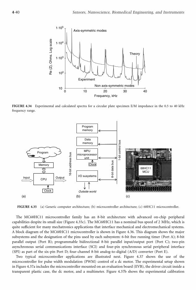
The MC68HC11 microcontroller family has an 8-bit architecture with advanced on-chip peripheral
capabilities despite its small size (Figure 4.35c). The MC68HC11 has a nominal bus speed of 2 MHz, which is
quite sufficient for many mechatronics applications that interface mechanical and electromechanical systems.
A block diagram of the MC68HC11 microcontroller is shown in Figure 4.36. This diagram shows the major
subsystems and the designation of the pins used by each subsystem: 6-bit free running timer (Port A); 8-bit
parallel output (Port B); programmable bidirectional 8-bit parallel input/output port (Port C); two-pin
asynchronous serial communications interface (SCI) and four-pin synchronous serial peripheral interface
(SPI) as part of the six-pin Port D; four-channel 8-bit analog-to-digital (A/D) converter (Port E).
Two typical microcontroller applications are illustrated next. Figure 4.37 shows the use of the
microcontroller for pulse width modulation (PWM) control of a dc motor. The experimental setup shown
in Figure 4.37a includes the microcontroller mounted on an evaluation board (EVB), the driver circuit inside a
transparent plastic case, the dc motor, and a multimeter. Figure 4.37b shows the experimental calibration
0 10 20 30 4010
100
1.103
1.104
1.105
Frequency, kHz
Re
(Z),
Ohm
s.Lo
gsc
ale
Axis-symmetric modes
Theory
Experiment
Non axis-symmetric modes
FIGURE 4.34 Experimental and calculated spectra for a circular plate specimen E/M impedance in the 0.5 to 40 kHz
frequency range.
Program
Memory
CPUOutputInput
Clock
Programmemory
Datamemory
MPUmicroprocessor
unit
I/O susystems
Clock
16-b
itad
dres
sbu
s
1-bi
tcon
trol
bus
8-bi
tdat
abu
s
Outside world
(a) (b) (c)
68HC11MCU
FIGURE 4.35 (a) Generic computer architecture; (b) microcontroller architecture; (c) 68HC11 microcontroller.
4-40 Sensors, Nanoscience, Biomedical Engineering, and Instruments
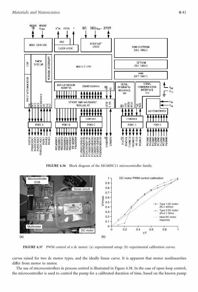
curves raised for two dc motor types, and the ideally linear curve. It is apparent that motor nonlinearities
differ from motor to motor.
The use of microcontrollers in process control is illustrated in Figure 4.38. In the case of open-loop control,
the microcontroller is used to control the pump for a calibrated duration of time, based on the known pump
FIGURE 4.36 Block diagram of the MC68HC11 microcontroller family.
DC motorMultimeter
Driver circuit
MicrocontrollerEVB
DC motor PWM control calibration
0
0.1
0.2
0.3
0.4
0.5
0.6
0.7
0.8
0.9
1
0 0.2 0.4 0.6 0.8 1t/T
V/V
max
Type 1 DC motor(R=1.3Ohm)Type 2 DC motor(R=4.1 Ohm)
Ideal DC motorresponse
(a) (b)
FIGURE 4.37 PWM control of a dc motor: (a) experimental setup; (b) experimental calibration curves.
4-41Materials and Nanoscience
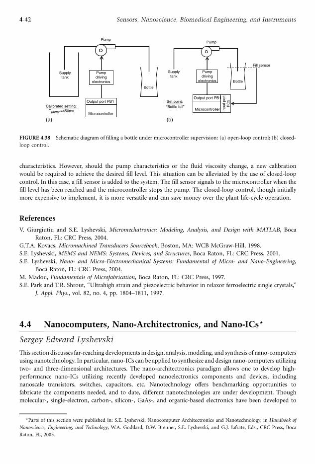
characteristics. However, should the pump characteristics or the fluid viscosity change, a new calibration
would be required to achieve the desired fill level. This situation can be alleviated by the use of closed-loop
control. In this case, a fill sensor is added to the system. The fill sensor signals to the microcontroller when the
fill level has been reached and the microcontroller stops the pump. The closed-loop control, though initially
more expensive to implement, it is more versatile and can save money over the plant life-cycle operation.
References
V. Giurgiutiu and S.E. Lyshevski, Micromechatronics: Modeling, Analysis, and Design with MATLAB, Boca
Raton, FL: CRC Press, 2004.
G.T.A. Kovacs, Micromachined Transducers Sourcebook, Boston, MA: WCB McGraw-Hill, 1998.
S.E. Lyshevski, MEMS and NEMS: Systems, Devices, and Structures, Boca Raton, FL: CRC Press, 2001.
S.E. Lyshevski, Nano- and Micro-Electromechanical Systems: Fundamental of Micro- and Nano-Engineering,
Boca Raton, FL: CRC Press, 2004.
M. Madou, Fundamentals of Microfabrication, Boca Raton, FL: CRC Press, 1997.
S.E. Park and T.R. Shrout, ‘‘Ultrahigh strain and piezoelectric behavior in relaxor ferroelectric single crystals,’’
J. Appl. Phys., vol. 82, no. 4, pp. 1804–1811, 1997.
4.4 Nanocomputers, Nano-Architectronics, and Nano-ICs*
Sergey Edward Lyshevski
This section discusses far-reaching developments in design, analysis, modeling, and synthesis of nano-computers
using nanotechnology. In particular, nano-ICs can be applied to synthesize and design nano-computers utilizing
two- and three-dimensional architectures. The nano-architectronics paradigm allows one to develop high-
performance nano-ICs utilizing recently developed nanoelectronics components and devices, including
nanoscale transistors, switches, capacitors, etc. Nanotechnology offers benchmarking opportunities to
fabricate the components needed, and to date, different nanotechnologies are under development. Though
molecular-, single-electron, carbon-, silicon-, GaAs-, and organic-based electronics have been developed to
Output port PB1
Microcontroller
Pumpdriving
electronics
Calibrated setting:Tpump =450ms
Supplytank
Bottle
Pump
Pumpdriving
electronics
Set point:“Bottle full”
Supplytank
Bottle
Pump
Fill sensor
Output port PB1
Microcontroller Inpu
tpor
tP
C5
(a) (b)
FIGURE 4.38 Schematic diagram of filling a bottle under microcontroller supervision: (a) open-loop control; (b) closed-
loop control.
*Parts of this section were published in: S.E. Lyshevski, Nanocomputer Architectronics and Nanotechnology, in Handbook of
Nanoscience, Engineering, and Technology, W.A. Goddard, D.W. Brenner, S.E. Lyshevski, and G.J. Iafrate, Eds., CRC Press, Boca
Raton, FL, 2003.
4-42 Sensors, Nanoscience, Biomedical Engineering, and Instruments

fabricate nanodevices, and promising pioneering results have been reported, it is difficult to accurately predict
and envision the most promising high-yield affordable technologies and processes. Correspondingly, while
covering some nanotechnologies to fabricate nanodevices and nano-ICs, this section focuses on the advanced
concepts in fundamental and applied research in nanocomputers synthesis, design, and analysis. Mathematical
models are developed using nanodevices and nano-ICs behavior description. The models proposed are
straightforwardly applied to perform analysis, design, simulation, and optimization of nanocomputers.
Novel methods in design of nanocomputers and their components are documented. Fundamental and
applied results documented expand the horizon of nanocomputer theory and practice. It is illustrated that high-
performance nanocomputers can be devised and designed using nano-ICs integrated within the
nanoarchitectronics concept to synthesize two- and three-dimensional computer topologies with novel robust
fault-tolerant organizations.
Introduction
Recently, meaningful applied and experimental results in nanoelectronic have been reported [1–15]. Though
fundamental research has been performed in analysis of nanodevices, a limited number of feasible technologies
has been developed to date to design applicable nanodevices operating at room temperature. However, the
progress made in integrated carbon/silicon-based technology provides the confidence that nanoscale devices
will be mass-produced in the nearest future. Unfortunately, no perfect nanodevices and large-scale nanodevice
assemblies (matrices) can be fabricated. Correspondingly, novel adaptive and robust computing
architectures, topologies, and organizations must be devised and developed. Our goal is to further expand
and apply the fundamental theory of nanocomputers, develop the basic research toward sound nanocomputer
theory and practice, as well as report the application of nanotechnology to fabricate nanocomputers and their
components.
Several types of nanocomputers have been proposed. For the last one thousand years the synthesis and design
of computers have been performed as a sequence of different paradigms and changes, e.g., from gears to relays,
then to valves and to transistors, and more recently (in the 1980s) to integrated circuits [16]. Currently, IC
technology progressed to the point that hundreds of millions of transistors are fabricated on a 1 cm2 silicon
chips. The transistors are downsized to hundreds of nanometers using 50- and 70-nm fabrication technologies.
However, the silicon-based technology reaching the limit, and scaling laws cannot be applied due to the
fundamental limitations and basic physics [17–26]. Nanotechnology allows one to fabricate nanoscale
transistors that operate based on the quantum mechanics paradigms. Furthermore, computing can be
performed utilizing quantum principles. Digital computers use bits (charged is 1 and not charged is 0). A
register of 3 bits is represented by eight numbers, e.g., 000, 001, 010, 100, 011, 101, 110, and 111. In the quantum
state (quantum computing), an atom (1 bit) can be in two places at once according to the laws of quantum
physics. Therefore, two atoms (quantum bits or qubits) can represent eight numbers at any given time. For x
number of qubits, 2x numbers are stored. Parallel processing can take place on the 2x input numbers, performing
the same task that a classical computer would have to repeat 2x times or use 2x processors working in parallel.
Therefore, a quantum computer offers an enormous gain in the use of computational resources in terms of time
and memory. Unfortunately, limited progress has been made to date in practical application of this concept.
Though conventional computers require exponentially more time and memory to match the power of a
quantum computer, it is unlikely that quantum computers will become the reality in the near observable future.
Correspondingly, experimental, applied, and fundamental research in nanocomputers has been performed to
significantly increase the computational and processing speed, memory, and other performance characteristics
utilizing novel nanodevices through application of nanotechnology (rather than solely rely on the quantum
computing and possible quantum computers due to existing formidable challenges). Nanocomputers will allow
one to compute and process information thousands of times faster than advanced computers.
Bioelectrochemical nanocomputers store and process information utilizing complex electrochemical
interactions and changes. Bioelectrochemical nanobiocircuits that store, process, and compute exist in nature
in enormous variety and complexity evolving through thousands of years of evolution. The development and
prototyping of bioelectrochemical nanocomputer and three-dimensional circuits have progressed through
4-43Materials and Nanoscience
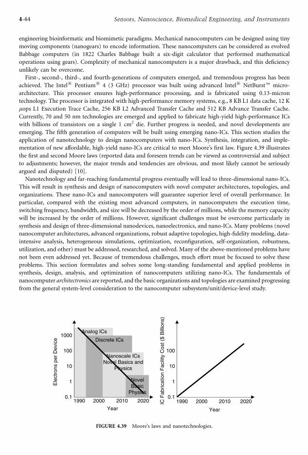
engineering bioinformatic and biomimetic paradigms. Mechanical nanocomputers can be designed using tiny
moving components (nanogears) to encode information. These nanocomputers can be considered as evolved
Babbage computers (in 1822 Charles Babbage built a six-digit calculator that performed mathematical
operations using gears). Complexity of mechanical nanocomputers is a major drawback, and this deficiency
unlikely can be overcome.
First-, second-, third-, and fourth-generations of computers emerged, and tremendous progress has been
achieved. The Intel1 Pentium1 4 (3 GHz) processor was built using advanced Intel1 NetBurste micro-
architecture. This processor ensures high-performance processing, and is fabricated using 0.13-micron
technology. The processor is integrated with high-performance memory systems, e.g., 8 KB L1 data cache, 12 K
mops L1 Execution Trace Cache, 256 KB L2 Advanced Transfer Cache and 512 KB Advance Transfer Cache.
Currently, 70 and 50 nm technologies are emerged and applied to fabricate high-yield high-performance ICs
with billions of transistors on a single 1 cm2 die. Further progress is needed, and novel developments are
emerging. The fifth generation of computers will be built using emerging nano-ICs. This section studies the
application of nanotechnology to design nanocomputers with nano-ICs. Synthesis, integration, and imple-
mentation of new affordable, high-yield nano-ICs are critical to meet Moore’s first law. Figure 4.39 illustrates
the first and second Moore laws (reported data and foreseen trends can be viewed as controversial and subject
to adjustments; however, the major trends and tendencies are obvious, and most likely cannot be seriously
argued and disputed) [10].
Nanotechnology and far-reaching fundamental progress eventually will lead to three-dimensional nano-ICs.
This will result in synthesis and design of nanocomputers with novel computer architectures, topologies, and
organizations. These nano-ICs and nanocomputers will guarantee superior level of overall performance. In
particular, compared with the existing most advanced computers, in nanocomputers the execution time,
switching frequency, bandwidth, and size will be decreased by the order of millions, while the memory capacity
will be increased by the order of millions. However, significant challenges must be overcome particularly in
synthesis and design of three-dimensional nanodevices, nanoelectronics, and nano-ICs. Many problems (novel
nanocomputer architectures, advanced organizations, robust adaptive topologies, high-fidelity modeling, data-
intensive analysis, heterogeneous simulations, optimization, reconfiguration, self-organization, robustness,
utilization, and other) must be addressed, researched, and solved. Many of the above-mentioned problems have
not been even addressed yet. Because of tremendous challenges, much effort must be focused to solve these
problems. This section formulates and solves some long-standing fundamental and applied problems in
synthesis, design, analysis, and optimization of nanocomputers utilizing nano-ICs. The fundamentals of
nanocomputer architectronics are reported, and the basic organizations and topologies are examined progressing
from the general system-level consideration to the nanocomputer subsystem/unit/device-level study.
Ele
ctro
nspe
rD
evic
e
Analog ICs
Year
1000
100
10
1
0.11990 2000 2010 2020
Discrete ICs
Nanoscale ICsNovel Basics and
Physics
Year
100
10
1
0.11990 2000 2010 2020IC
Fab
ricat
ion
Fac
ility
Cos
t($
Bill
ions
)
NovelBasic
Physics
FIGURE 4.39 Moore’s laws and nanotechnologies.
4-44 Sensors, Nanoscience, Biomedical Engineering, and Instruments
Nano-Electronics and Nanocomputer Fundamentals
In general, both reversible and irreversible nanocomputers can be designed. Nowadays, all existing computers
are irreversible. The system is reversible if it is deterministic in the reverse and forward time directions. The
reversibility implies that no physical state can be reached by more than one path (otherwise, reverse evolution
would be nondeterministic). Current computers constantly irreversibly erase temporary results, and thus the
entropy changes. The average instruction execution speed (in millions of instructions executed per second, IPS)
and cycles per instruction are related to the time required to execute instructions as given by Tinst¼ 1/fclock. The
clock frequency fclock depends mainly on the ICs or nano-ICs used as well as upon the fabrication technologies
(for example, the switching frequency 3 GHz was achieved in the existing Intel Pentium processors). The
quantum mechanics implies an upper limit on the frequency at which the system can switch from one state to
another. This limit is found as the difference between the total energy E of the system and ground state energy E0.
We have the following explicit inequality to find themaximum switching frequency f14
hðE E0Þ. Here, h is the
Planck constant, and h¼ 6.626610 34 J sec or J/Hz. An isolated nanodevice, consisting of a single electron at a
potential of 1 V above its ground state, contains 1 eV of energy (1 eV ¼ 1.602610 19 J) and therefore cannot
change its state faster than f14
hðE E0Þ ¼ 4
6:626 10 34 1:602 10 19 0:97 1015 Hz. For example, the
switching frequency can be achieved in the range up to 161015 Hz. We conclude that the switching frequency
of nano-ICs can be significantly increased compared with currently used CMOS technology-based ICs.
In asymptotically reversible nanocomputers, the generated entropy is found as S ¼ b/tt, where b is the
entropy coefficient that varies from 16107 to 16106 bits/GHz for ICs, and from 1 to 10 bits/GHz for
quantum FETs; tt is the length of time over which the operation is performed. Hence, the minimum entropy
and processing (operation) rate for quantum nanodevices are S ¼ 1 bit/operation and re ¼ 161026
operation/sec cm2, while CMOS technology allows one to fabricate devices with S ¼ 16106 bits/operation
and re ¼ 3.561016 operation/sec cm2.
The nanocomputer architecture integrates the functional, interconnected, and controlled hardware units
and systems that perform propagation (flow), storage, execution, and processing of information (data).
Nanocomputer accepts digital or analog input information, processes and manipulates it according to a list of
internally stored machine instructions, stores the information, and produces the resulting output. The list of
instructions is called a program, and internal storage is called memory.
In general, nanocomputer architecture can be synthesized utilizing the following major systems: (1) input–
output, (2) memory, (3) arithmetic and logic, and (4) control units.
The input unit accepts information from electronic devices or other computers through the cards
(electromechanical devices, such as keyboards, can be also interfaced). The information received can be stored
in the memory, and then manipulated and processed by the arithmetic and logic unit (ALU). The results are
output using the output unit. Information flow, propagation, manipulation, processing, and storage
(memory) are coordinated by the control unit. The arithmetic and logic unit, integrated with the control unit,
is called the processor or central processing unit (CPU). Input and output systems are called the input–output
(I/O) unit. The memory unit integrates memory systems that stores programs and data. There are two main
classes of memory, called primary (main) and secondary memory. The primary memory is implemented using
nano-ICs that can consist of billions of nanoscale storage cells (each cell can store one bit of information).
These cells are accessed in groups of fixed size called words. The main memory is organized such that the
contents of one word can be stored or retrieved in one basic operation called a memory cycle. To provide
consistent direct access to any word in the main memory in the shortest time, a distinct address number is
associated with each word location. A word is accessed by specifying its address and issuing a control
command that starts the storage or retrieval process. The number of bits in a word is called the word length.
Word lengths vary, for example, from 16 to 64 bits. Personal computers and workstations usually have a few
million words in the main memory, while nanocomputers can have hundreds of millions of words with the
time required to access a word for reading or writing within the picosecond range. Although the main memory
is essential, it tends to be expensive and volatile. Therefore, nano-ICs can be effectively used to implement the
additional memory systems to store programs and data forming secondary memory.
4-45Materials and Nanoscience
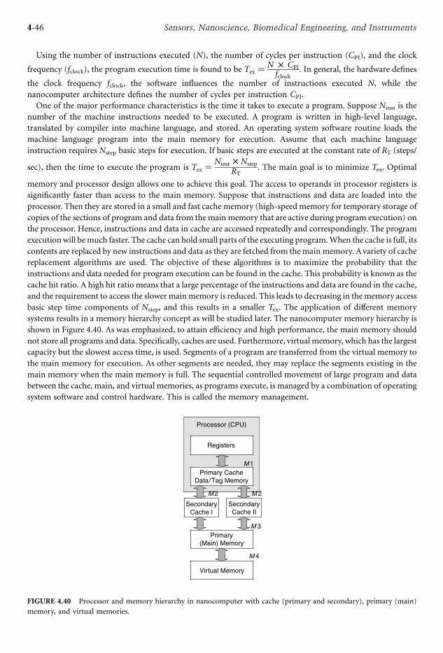
Using the number of instructions executed (N), the number of cycles per instruction (CPI), and the clock
frequency (fclock), the program execution time is found to be Tex ¼ N CPIfclock
. In general, the hardware defines
the clock frequency fclock, the software influences the number of instructions executed N, while the
nanocomputer architecture defines the number of cycles per instruction CPI.
One of the major performance characteristics is the time it takes to execute a program. Suppose Ninst is the
number of the machine instructions needed to be executed. A program is written in high-level language,
translated by compiler into machine language, and stored. An operating system software routine loads the
machine language program into the main memory for execution. Assume that each machine language
instruction requires Nstep basic steps for execution. If basic steps are executed at the constant rate of RT (steps/
sec), then the time to execute the program is Tex ¼ Ninst Nstep
RT. The main goal is to minimize Tex. Optimal
memory and processor design allows one to achieve this goal. The access to operands in processor registers is
significantly faster than access to the main memory. Suppose that instructions and data are loaded into the
processor. Then they are stored in a small and fast cache memory (high-speed memory for temporary storage of
copies of the sections of program and data from the main memory that are active during program execution) on
the processor. Hence, instructions and data in cache are accessed repeatedly and correspondingly. The program
executionwill bemuch faster. The cache can hold small parts of the executing program.When the cache is full, its
contents are replaced by new instructions and data as they are fetched from the main memory. Avariety of cache
replacement algorithms are used. The objective of these algorithms is to maximize the probability that the
instructions and data needed for program execution can be found in the cache. This probability is known as the
cache hit ratio. A high hit ratio means that a large percentage of the instructions and data are found in the cache,
and the requirement to access the slowermainmemory is reduced. This leads to decreasing in thememory access
basic step time components of Nstep, and this results in a smaller Tex. The application of different memory
systems results in a memory hierarchy concept as will be studied later. The nanocomputer memory hierarchy is
shown in Figure 4.40. As was emphasized, to attain efficiency and high performance, the main memory should
not store all programs and data. Specifically, caches are used. Furthermore, virtual memory, which has the largest
capacity but the slowest access time, is used. Segments of a program are transferred from the virtual memory to
the main memory for execution. As other segments are needed, they may replace the segments existing in the
main memory when the main memory is full. The sequential controlled movement of large program and data
between the cache, main, and virtual memories, as programs execute, is managed by a combination of operating
system software and control hardware. This is called the memory management.
Processor (CPU)
Primary CacheData/Tag Memory
SecondaryCache I
Primary(Main) Memory
Virtual Memory
SecondaryCache II
Registers
M1
M 2 M 2
M 3
M 4
FIGURE 4.40 Processor and memory hierarchy in nanocomputer with cache (primary and secondary), primary (main)
memory, and virtual memories.
4-46 Sensors, Nanoscience, Biomedical Engineering, and Instruments
Using the memory hierarchy illustrated in Figure 4.40, the CPU communicates directly only with M1, and
M1 communicates withM2, and so on. Therefore, for the CPU to assess the information, stored in the memory
Mj, requires the sequence of j data transfer as given by
Mj 1 :¼ Mj;Mj 2 :¼ Mj 1; . . .M1 :¼ M2; CPU :¼ M1
However, the memory bypass can be implemented and effectively used.
To perform computing, specific programs consisting of a set of machine instructions are stored in the main
memory. Individual instructions are fetched from the memory into the processor for execution. Data used as
operands are also stored in the memory. The connection between the main memory and the processor that
guarantees the transfer of instructions and operands is called the bus. A bus consists of a set of address, data,
and control lines. The bus permits transfer of program and data files from their long-term location (virtual
memory) to the main memory. Communication with other computers is ensured by transferring the data
through the bus. Normal execution of programs may be preempted if some IO device requires urgent control.
To perform this, specific programs are executed, and the device sends an interrupt signal to the processor. The
processor temporarily suspends the program that is being executed, and executes the special interrupt service
routine instead. After providing the required interrupt service, the processor switches back to the interrupted
program. During program loading and execution, the data should be transferred between the main memory
and secondary memory. This is performed using the direct memory access.
Nanocomputers can be classified using different classification principles. For example, making use of the
multiplicity of instruction and data streams, the following classification can be applied:
1. Single instruction stream/single data stream—conventional word-sequential architecture including
pipelined nanocomputers with parallel arithmetic logic unit (ALU)
2. Single instruction stream/multiple data stream—multiple ALU architectures, e.g., parallel-array
processor (ALU can be either bit-serial or bit-parallel)
3. Multiple instruction stream/single data stream
4. Multiple instruction stream/multiple data stream—the multiprocessor system with multiple control unit
The execution of most operations is performed by the ALU. In the ALU, the logic nanogates and
nanoregisters used to perform the basic operations (addition, subtraction, multiplication, and division) of
numeric operands, and the comparison, shifting, and alignment operations of general forms of numeric and
nonnumeric data. The processors contain a number of high-speed registers, which are used for temporary
storage of operands. A register, as a storage device for words, is a key sequential component, and registers are
connected. Each register contains one word of data and its access time at least ten times faster than the main
memory access time. A register-level system consists of a set of registers connected by combinational data-
processing and data-processing nano-ICs. Each operation is implemented as given by the following statement:
cond: X:¼ f ðx1; x2; . . . ; xi 1; xiÞThus, when the condition cond holds, compute the combinational function of f on x1, x2, . . ., xi 1, xi and
assign the resulting value to X. Here, cond is the control condition prefix which denotes the condition that
must be satisfied; X, x1, x2, . . ., xi 1, xi are the data words or the registers that store them; f is the function to be
performed within a single clock cycle.
Suppose that two numbers located in the main memory should be multiplied, and the sum must be stored
back into thememory. Using instructions, determined by the control unit, the operands are first fetched from the
memory into the processor. They are then multiplied in the ALU, and the result is stored back in memory.
Various nano-ICs can be used to execute data-processing instructions. The complexity of the ALU is determined
by the arithmetic instruction implementation. For example, ALUs that perform fixed-point addition, subtrac-
tion, and word-based logic can be implemented as combinational nano-ICs. The floating-point arithmetic
requires complex implementation and arithmetic coprocessors to perform complex numerical functions
needed. The floating-point numerical value of a number X is (Xm, Xe), where Xm is the mantissa and Xe is the
fixed-point number. Using the base b (usually, b ¼ 2), we have X ¼ Xm b xe . Therefore, the general basic
operations are quite complex and some problems (biasing, overflow, underflow, etc.) must be resolved.
4-47Materials and Nanoscience
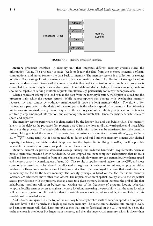
Memory–processor interface—A memory unit that integrates different memory systems stores the
information (data). The processor accesses (reads or loads) the data from the memory systems, performs
computations, and stores (writes) the data back to memory. The memory system is a collection of storage
locations. Each storage location (memory word) has a numerical address. A collection of storage locations
forms an address space. Figure 4.41 documents the data flow and its control, representing how a processor is
connected to a memory system via address, control, and data interfaces. High-performance memory systems
should be capable of serving multiple requests simultaneously, particularly for vector nanoprocessors.
When a processor attempts to load or read the data from the memory location, the request is issued and the
processor stalls while the request returns. While nanocomputers can operate with overlapping memory
requests, the data cannot be optimally manipulated if there are long memory delays. Therefore, a key
performance parameter in the design of nanocomputer is the effective speed of its memory. The following
limitations are imposed on any memory systems: the memory cannot be infinitely large, cannot contain an
arbitrarily large amount of information, and cannot operate infinitely fast. Hence, the major characteristics are
speed and capacity.
The memory system performance is characterized by the latency (tl) and bandwidth (Bw). The memory
latency is the delay as the processor first requests a word from memory until that word arrives and is available
for use by the processor. The bandwidth is the rate at which information can be transferred from the memory
system. Taking note of the number of requests that the memory can service concurrently Nrequest, we have
Bw ¼ Nrequesttl . Using nano-ICs, it become feasible to design and build superior memory systems with desired
capacity, low latency, and high bandwidth approaching the physical limits. Using nano-ICs, it will be possible
to match the memory and processor performance characteristics.
Memory hierarchies provide decreased average latency and reduced bandwidth requirements, whereas
parallel memories provide higher bandwidth. As was emphasized, nanocomputer architectures that utilize a
small and fast memory located in front of a large but relatively slow memory, can tremendously enhance speed
and memory capacity by making use of nano-ICs. This results in application of registers in the CPU, and most
commonly accessed variables should be allocated at registers. A variety of techniques, employing either
hardware, software, or a combination of hardware and software, are employed to ensure that most references
to memory are fed by the faster memory. The locality principle is based on the fact that some memory
locations are referenced more often than others. The implementation of spatial locality, due to the sequential
access, provides one with the property that an access to a given memory location increases the probability that
neighboring locations will soon be accessed. Making use of the frequency of program looping behavior,
temporal locality ensures access to a given memory location, increasing the probability that the same location
will be accessed again soon. It is evident that if a variable was not referenced for a while, it is unlikely that this
variable will be needed soon.
As illustrated in Figure 4.40, the top of the memory hierarchy level consists of superior speed CPU registers.
The next level in the hierarchy is a high-speed cache memory. The cache can be divided into multiple levels,
and nanocomputers will likely have multiple caches that can be fabricated on the CPU nanochip. Below the
cache memory is the slower but larger main memory, and then the large virtual memory, which is slower than
Processor (CPU)
Address
Control
Data
MemorySystem
Instructions
FIGURE 4.41 Memory–processor interface.
4-48 Sensors, Nanoscience, Biomedical Engineering, and Instruments
the main memory. These levels can be designed and fabricated utilizing different nano-ICs. Three performance
characteristics (access time, bandwidth, and capacity) and many factors (affordability, robustness, adaptability,
reconfigurability, etc.) support the application of multiple levels of cache memory and the memory hierarchy
concept. The time needed to access the primary cache should match with the clock frequency of the CPU,
and the corresponding nano-ICs must be used. We place a smaller first-level (primary) cache above a larger
second-level (secondary) cache. The primary cache is accessed quickly, and the secondary cache holds more
data close to the CPU. The nanocomputer architecture, built using nanoelectronics integrated within nano-ICs
assemblies, depends on the technologies available. For example, primary cache can be fabricated on the CPU
chip, while the secondary caches can be an on- or out-of-chip solution.
Size, speed, latency, bandwidth, power consumption, robustness, affordability, and other performance
characteristics are examined to guarantee the desired overall nanocomputer performance based upon the
specifications imposed. The performance parameter, which can be used to quantitatively examine different
memory systems, is the effective latency tef. We have:
tef ¼ thitRhit þ tmissð1 RhitÞ;where thit and tmiss are the hit and miss latencies, Rhit is the hit ratio, and Rhit , 1.
If the needed word is found in a level of the hierarchy, it is called a hit. Correspondingly, if a request must be
sent to the next lower level, the request is said to be a miss. The miss ratio is given as Rmiss ¼ (1 – Rhit). These
Rhit and Rmiss ratios are strongly influenced by the program being executed and influenced by the high-/low-
level memory capacity ratio. The access efficiency Eef of multiple-level memory (i – 1 and i) is found using the
access time, and hit and miss ratios. In particular:
Eef ¼ 1taccess time i 1
taccess time iRmiss þ Rhit
The hardware can dynamically allocate parts of the cache memory for addresses likely to be accessed soon. The
cache contains only redundant copies of the address space. The cache memory can be associative or content-
addressable. In an associative memory, the address of a memory location is stored along with its content.
Rather than reading data directly from a memory location, the cache is given an address and responds by
providing data that might or might not be the data requested. When a cache miss occurs, the memory access is
then performed from main memory, and the cache is updated to include the new data. The cache should hold
the most active portions of the memory, and the hardware dynamically selects portions of main memory to
store in the cache. When the cache is full, some data must be transferred to the main memory or deleted.
Therefore, a strategy for cache memory management is needed. Cache management strategies are based on the
locality principle. In particular, spatial (selection of what is brought into the cache) and temporal (selection of
what must be removed) localities are embedded. When a cache miss occurs, hardware copies a contiguous
block of memory into the cache, which includes the word requested. This fixed-size memory block can be
small (bit or word) or hundreds of bytes. Caches can require all fixed-size memory blocks to be aligned. When
a fixed-size memory block is brought into the cache, it is likely that another fixed-size memory block must be
removed. The selection of the removed fixed-size memory block is based on the effort to capture temporal
locality. In general, this is difficult to achieve. Correspondingly, viable methods are used to predict future
memory accesses. A least-recently-used concept can be the preferred choice for nanocomputers.
The cache can integrate the data memory and the tag memory. The address of each cache line contained in the
data memory is stored in the tag memory (the state can also track which cache line is modified). Each line
contained in the data memory is allocated by a corresponding entry in the tag memory to indicate the full
address of the cache line. The requirement that the cache memory be associative (content-addressable)
complicates the design because addressing data by content is more complex than by its address (all tags must be
compared concurrently). The cache can be simplified by embedding a mapping of memory locations to cache
cells. This mapping limits the number of possible cells in which a particular line may reside. Each memory
4-49Materials and Nanoscience

location can be mapped to a single location in the cache through direct mapping. Although there is no choice of
where the line resides and which line must be replaced, however, poor utilization results. In contrast, a two-way
set-associative cache maps each memory location into either of two locations in the cache. Hence, this mapping
can be viewed as two identical directly mapped caches. In fact, both caches must be searched at each memory
access, and the appropriate data selected and multiplexed on a tag match hit and on a miss. Then, a choice
must be made between two possible cache lines as to which is to be replaced. A single least-recently-used bit can
be saved for each such pair of lines to remember which line has been accessed more recently. This bit must be
toggled to the current state each time. To this end, anM-way associative cache maps each memory location into
Mmemory locations in the cache. Therefore, this cachemap can be constructed fromM identical direct-mapped
caches. The problem of maintaining the least-recently-used ordering ofM cache lines is primarily due to the fact
that there areM! possible orderings. In fact, it takes at least log2 M! bits to store the ordering. It can be envisioned
that a two-, three-, or four-way associative cache will be implemented in nanocomputers.
Consider the write operation. If the main memory copy is updated with each write operation, then write-
through or store-through technique is used. If the main memory copy is not updated with each write
operation, write-back or copy-back or deferred writes algorithm is enforced. In general, the cache coherence or
consistency problem must be examined due to the implementation of different bypass techniques.
Parallel Memories—Main memories can comprise a series of memory nanochips or nano-ICs on a single
nanochip. These nano-ICs form a nanobank. Multiple memory nanobanks can be integrated together to form
a parallel main memory system. Since each nanobank can service a request, a parallel main memory system
with Nmb nanobanks can service Nmb requests simultaneously, increasing the bandwidth of the memory
system by Nmb times the bandwidth of a single nanobank. The number of nanobanks is a power of 2, that is,
Nmb ¼ 2p. An n-bit memory word address is broken into two parts: a p-bit nanobank number and an m-bit
address of a word within a nanobank. The p bits used to select a nanobank number could be any p bits of the
n-bit word address. Let us use the low-order p address bits to select the nanobank number, and the higher
order m ¼ n – p bits of the word address is used to access a word in the selected nanobank.
Multiple memory nanobanks can be connected using simple paralleling and complex paralleling. Figure 4.42
shows the structure of a simple parallel memory system wherem address bits are simultaneously supplied to all
memory nanobanks. All nanobanks are connected to the same read/write control line. For a read operation,
the nanobanks perform the read operation and deposit the data in the latches. Data can then be read from the
latches one by one by setting the switch appropriately. The nanobanks can be accessed again to carry out
another read or write operation. For a write operation, the latches are loaded one by one. When all latches
have been written, their contents can be written into the memory nanobanks by supplying m bits of address. In
a simple parallel memory, all nanobanks are cycled at the same time. Each nanobank starts and completes its
m-address bits
Latches
...1 ... 2p
Nanobanks
... ... 2p
p-address bits(select switch)
c -bits data busSwitch
m -address bits
Nanobanks
i ...
Latches
1 ...
1 ...
i ...
p-address bits(select switch)
c -bits data busSwitch
Mem
ory
Con
trol
ler
i
i1
2p
2p
FIGURE 4.42 Simple and complex parallel main memory systems.
4-50 Sensors, Nanoscience, Biomedical Engineering, and Instruments
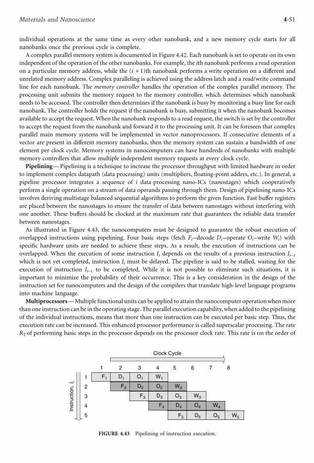
individual operations at the same time as every other nanobank, and a new memory cycle starts for all
nanobanks once the previous cycle is complete.
A complex parallel memory system is documented in Figure 4.42. Each nanobank is set to operate on its own
independent of the operation of the other nanobanks. For example, the ith nanobank performs a read operation
on a particular memory address, while the (i + 1)th nanobank performs a write operation on a different and
unrelated memory address. Complex paralleling is achieved using the address latch and a read/write command
line for each nanobank. The memory controller handles the operation of the complex parallel memory. The
processing unit submits the memory request to the memory controller, which determines which nanobank
needs to be accessed. The controller then determines if the nanobank is busy by monitoring a busy line for each
nanobank. The controller holds the request if the nanobank is busy, submitting it when the nanobank becomes
available to accept the request. When the nanobank responds to a read request, the switch is set by the controller
to accept the request from the nanobank and forward it to the processing unit. It can be foreseen that complex
parallel main memory systems will be implemented in vector nanoprocessors. If consecutive elements of a
vector are present in different memory nanobanks, then the memory system can sustain a bandwidth of one
element per clock cycle. Memory systems in nanocomputers can have hundreds of nanobanks with multiple
memory controllers that allow multiple independent memory requests at every clock cycle.
Pipelining—Pipelining is a technique to increase the processor throughput with limited hardware in order
to implement complex datapath (data processing) units (multipliers, floating-point adders, etc.). In general, a
pipeline processor integrates a sequence of i data-processing nano-ICs (nanostages) which cooperatively
perform a single operation on a stream of data operands passing through them. Design of pipelining nano-ICs
involves deriving multistage balanced sequential algorithms to perform the given function. Fast buffer registers
are placed between the nanostages to ensure the transfer of data between nanostages without interfering with
one another. These buffers should be clocked at the maximum rate that guarantees the reliable data transfer
between nanostages.
As illustrated in Figure 4.43, the nanocomputers must be designed to guarantee the robust execution of
overlapped instructions using pipelining. Four basic steps (fetch Fi–decode Di–operate Oi–write Wi) with
specific hardware units are needed to achieve these steps. As a result, the execution of instructions can be
overlapped. When the execution of some instruction Ii depends on the results of a previous instruction Ii–1which is not yet completed, instruction Ii must be delayed. The pipeline is said to be stalled, waiting for the
execution of instruction Ii–1 to be completed. While it is not possible to eliminate such situations, it is
important to minimize the probability of their occurrence. This is a key consideration in the design of the
instruction set for nanocomputers and the design of the compilers that translate high-level language programs
into machine language.
Multiprocessors—Multiple functional units can be applied to attain the nanocomputer operationwhenmore
than one instruction can be in the operating stage. The parallel execution capability, when added to the pipelining
of the individual instructions, means that more than one instruction can be executed per basic step. Thus, the
execution rate can be increased. This enhanced processor performance is called superscalar processing. The rate
RT of performing basic steps in the processor depends on the processor clock rate. This rate is on the order of
Inst
ruct
ion,
I i
1
1 8
F1 D1 O1 W1
F2 D2 O2 W2
F3 D3 O3 W3
F4 D4 O4 W4
F5 D5 O5 W5
2
3
4
5
Clock Cycle
765432
FIGURE 4.43 Pipelining of instruction execution.
4-51Materials and Nanoscience

billions steps per second in current high-performance nano-ICs. It was illustrated that physical limits prevent
single processors from being speeded up indefinitely. Nanocomputers with multiprocessors will speed up the
execution of large programs by executing subtasks in parallel. The main difficulty in achieving this is
decomposition of a given task into its parallel subtasks and ordering these subtasks to the individual processors in
such a way that communication among the subtasks will be performed efficiently and robustly. Figure 4.44
documents a block diagram of a multi-processor system with the interconnection network needed for data
sharing among the processors Pi. Parallel paths are needed in this network in order to parallel activity to proceed
in the processors as they access the global memory space represented by the multiple memory unitsMi.
Nanocomputer Architectronics—The theory of computing, computer architecture, and networking is the
study of efficient robust processing and communication, modeling, analysis, optimization, adaptive networks,
architecture, and organization synthesis, as well as other problems of hardware and software design. These studies
have emerged as a synergetic fundamental discipline (computer engineering and science), and many problems
have not been solved yet. Correspondingly, a large array of questions remains unanswered. Nanocomputer
architectonics is the theory of nanocomputers devised and designed using fundamental theory and applying
nano-ICs.Our goal is to develop the nanocomputer achitectronics basics, e.g., fundamentalmethods in synthesis,
design, analysis, modeling, computer-aided design, etc. Nanocomputer achitectronics, which is a computer
science and engineering frontier, will allow one to solve a wide spectrum of fundamental and applied problems.
Applying the nanocomputer achitectronics paradigm, this section spans the theory of nanocomputers and
related areas, e.g., information processing, communication paradigms, computational complexity theory,
combinatorial optimization, architecture synthesis, optimal organization, and their applications. Making of the
nanocomputer achitectronics paradigms, one can address and study fundamental problems in nanocomputer
architecture synthesis, design, and optimization applying three-dimensional organization, application of
nano-ICs, multithreading, error recovery, massively parallel computing organization, shared memory
parallelism, message passing parallelism, etc. The nanocomputer fundamentals, operation, and functionality
can be devised through neuroscience. The key to understand learning, adaptation, control, architecture,
hierarchy, organization, memory, intelligence, diagnostics, self-organization, computing, and other system-level
P1 M1
Interconnected Network for Multiprocessor Architecture
P2 M2 Pn −1 Mn −1 Pn Mn
FIGURE 4.44 Multiprocessor architecture. The basic parallel organization for nanocomputers is represented in Figure 4.45.
Control
Processor
Network IO
Memory
FIGURE 4.45 Parallel nanocomputer organization to maximize computer concurrency.
4-52 Sensors, Nanoscience, Biomedical Engineering, and Instruments
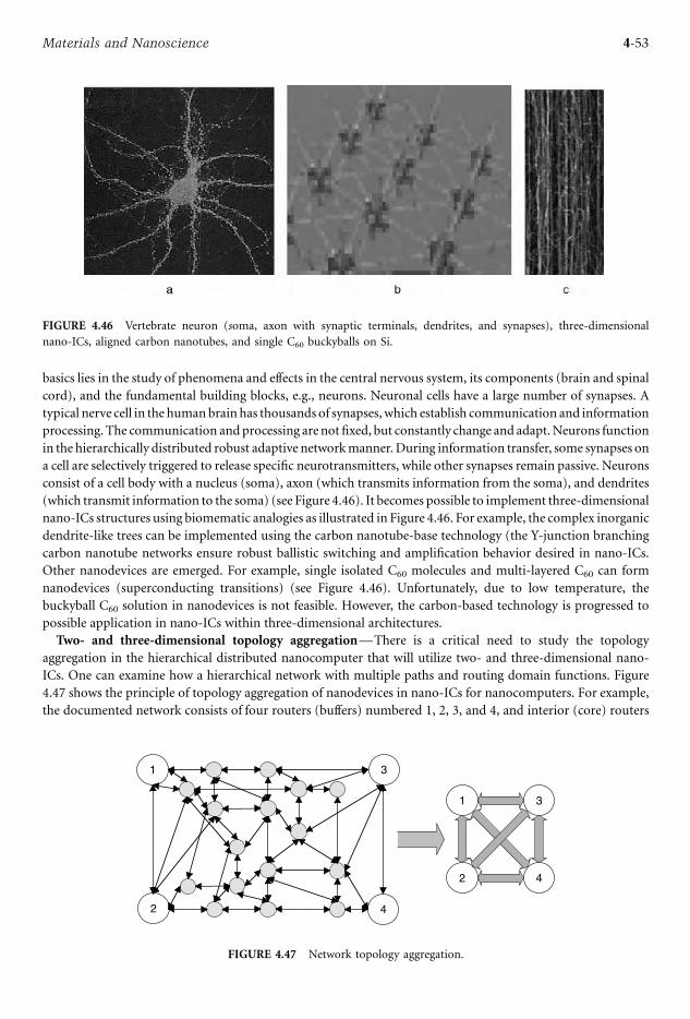
basics lies in the study of phenomena and effects in the central nervous system, its components (brain and spinal
cord), and the fundamental building blocks, e.g., neurons. Neuronal cells have a large number of synapses. A
typical nerve cell in the human brain has thousands of synapses, which establish communication and information
processing. The communication andprocessing are not fixed, but constantly change and adapt.Neurons function
in the hierarchically distributed robust adaptive networkmanner.During information transfer, some synapses on
a cell are selectively triggered to release specific neurotransmitters, while other synapses remain passive. Neurons
consist of a cell body with a nucleus (soma), axon (which transmits information from the soma), and dendrites
(which transmit information to the soma) (see Figure 4.46). It becomes possible to implement three-dimensional
nano-ICs structures using biomematic analogies as illustrated in Figure 4.46. For example, the complex inorganic
dendrite-like trees can be implemented using the carbon nanotube-base technology (the Y-junction branching
carbon nanotube networks ensure robust ballistic switching and amplification behavior desired in nano-ICs.
Other nanodevices are emerged. For example, single isolated C60 molecules and multi-layered C60 can form
nanodevices (superconducting transitions) (see Figure 4.46). Unfortunately, due to low temperature, the
buckyball C60 solution in nanodevices is not feasible. However, the carbon-based technology is progressed to
possible application in nano-ICs within three-dimensional architectures.
Two- and three-dimensional topology aggregation—There is a critical need to study the topology
aggregation in the hierarchical distributed nanocomputer that will utilize two- and three-dimensional nano-
ICs. One can examine how a hierarchical network with multiple paths and routing domain functions. Figure
4.47 shows the principle of topology aggregation of nanodevices in nano-ICs for nanocomputers. For example,
the documented network consists of four routers (buffers) numbered 1, 2, 3, and 4, and interior (core) routers
1
2
3
4
1
2
3
4
FIGURE 4.47 Network topology aggregation.
FIGURE 4.46 Vertebrate neuron (soma, axon with synaptic terminals, dendrites, and synapses), three-dimensional
nano-ICs, aligned carbon nanotubes, and single C60 buckyballs on Si.
4-53Materials and Nanoscience

are illustrated. After the aggregation, a meshed network with four nodes represents the same topology. The
difficulty in topology aggregation is to calculate the link metrics to attain the accuracy and to synthesize
optimized network topologies. The aggregated link metrics can be computed using the methods used for
multiplayer artificial networks. The bandwidth and delay are integrated to optimize the hierarchically
distributed networks. We believe that the distributed-memory nanocomputers can be adaptively configured
and reconfigured based upon processing, communication, and control (instruction) parallelisms.
Nanocomputer Architecture
System-level performance analysis is based on mathematical models used to examine nanocomputers and
optimize their architectures, organization, topologies, and parameters, as well as to perform optimal
hardware-software codesign. Computers process inputs, producing outputs accordingly. To examine the
performance, one should develop and apply the mathematical model of a nanocomputer which comprises
central processing, memory, input–output control, and other units. However, one cannot develop the
mathematical model without explicitly specifying the nanocomputer architecture, identifying the optimal
organization, and synthesizing the topologies. There are different levels of abstraction for nanocomputer
architectures, organizations, models, etc.
Advanced nanocomputer architectures (beyond Von Neumann computer architecture) can be devised to
guarantee superior processing and communication speed. Novel nanodevices that utilize new effects and
phenomena to perform computing and communication are sought. For example, through quantum
computing, the information can be stored in the phase of wavefunctions, and this concept leads to utilization
of massive parallelism of these wavefunctions to achieve enormous processing speed.
The CPU executes sequences of instructions and operands, which are fetched by the program control unit
(PCU), executed by the data processing unit (DPU), and then placed in memory. In particular, caches (high-
speed memory where data is copied when it is retrieved from the random access memory improving the
overall performance by reducing the average memory access time) are used. The instructions and data form
instruction and data streams which flow to and from the processor. The CPU may have two or more
processors and coprocessors with various execution units and multi-level instruction and data caches. These
processors can share or have their own caches. The CPU datapath contains nano-ICs to perform arithmetic
and logical operations on words such as fixed- or floating-point numbers. The CPU design involves trade-off
analysis between the hardware, speed, and affordability. The CPU is usually partitioned on the control and
datapath units, and the control unit selects and sequence the data-processing operations. The core interface
unit is a switch that can be implemented as autonomous cache controllers operating concurrently and feeding
the specified number (32, 64, or 128) of bytes of data per cycle. This core interface unit connects all controllers
to the data or instruction caches of processors. Additionally, the core interface unit accepts and sequences
information from the processors. A control unit is responsible for controlling data flow between controllers
that regulate the in and out information flows. There is the interface to input/output devices. On-chip debug,
error detection, sequencing logic, self-test, monitoring, and other units must be integrated to control a
pipelined nanocomputer. The computer performance depends on the architecture and hardware components
(which are discussed in this chapter). Figure 4.48 illustrates the possible nanocomputer organization.
In general, nanodevices ensure high density, superior bandwidth, high switching frequency, low power, etc.
It is envisioned that in the near future nanocomputers will allow one to increase the computing speed by a
factor of millions compared with the existing CMOS ICs computers. Three-dimensional, multiple-layered,
high-density nano-IC assemblies, shown in Figure 4.49, are envisioned to be used. Unfortunately, the number
of formidable fundamental, applied, experimental, and technological challenges arise, e.g., robust operation
and characteristics of nano-ICs are significantly affected by the ‘‘second-order’’ effects (gate oxide and bandgap
tunneling, energy quantization, electron transport, etc., and, furthermore, the operating principles for
nanodevices can be based on the quantum effects), noise vulnerability, complexity, etc. It is well known that
high-fidelity modeling, data-intensive analysis, heterogeneous simulation, and other fundamental issues even
for a single nanodevice are not completely solved yet. In addition, the currently existing fabrication processes
and technologies do not allow one to fabricate ideal nanodevices and nanostructures. In fact, even molecular
4-54 Sensors, Nanoscience, Biomedical Engineering, and Instruments
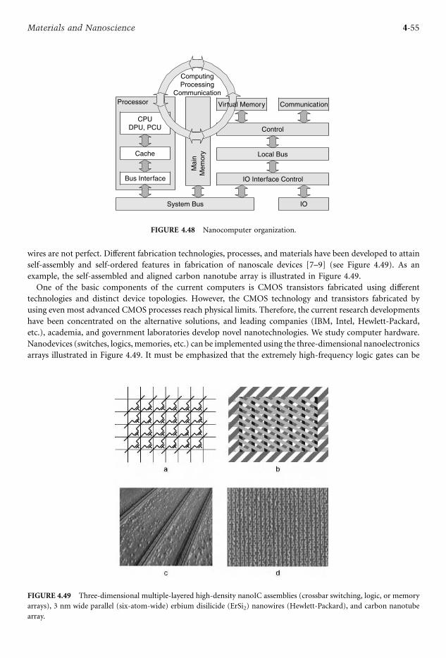
wires are not perfect. Different fabrication technologies, processes, and materials have been developed to attain
self-assembly and self-ordered features in fabrication of nanoscale devices [7–9] (see Figure 4.49). As an
example, the self-assembled and aligned carbon nanotube array is illustrated in Figure 4.49.
One of the basic components of the current computers is CMOS transistors fabricated using different
technologies and distinct device topologies. However, the CMOS technology and transistors fabricated by
using even most advanced CMOS processes reach physical limits. Therefore, the current research developments
have been concentrated on the alternative solutions, and leading companies (IBM, Intel, Hewlett-Packard,
etc.), academia, and government laboratories develop novel nanotechnologies. We study computer hardware.
Nanodevices (switches, logics, memories, etc.) can be implemented using the three-dimensional nanoelectronics
arrays illustrated in Figure 4.49. It must be emphasized that the extremely high-frequency logic gates can be
FIGURE 4.49 Three-dimensional multiple-layered high-density nanoIC assemblies (crossbar switching, logic, or memory
arrays), 3 nm wide parallel (six-atom-wide) erbium disilicide (ErSi2) nanowires (Hewlett-Packard), and carbon nanotube
array.
CPUDPU, PCU
Cache
Bus Interface
Control
Communication
Local Bus
IO Interface Control
IOSystem Bus
Processor Virtual Memory
ComputingProcessing
Communication
Mai
nM
emor
y
FIGURE 4.48 Nanocomputer organization.
4-55Materials and Nanoscience
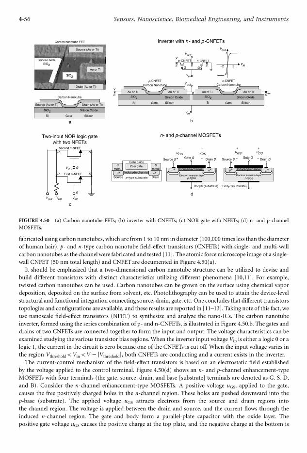
fabricated using carbon nanotubes, which are from 1 to 10 nm in diameter (100,000 times less than the diameter
of human hair). p- and n-type carbon nanotube field-effect transistors (CNFETs) with single- and multi-wall
carbon nanotubes as the channel were fabricated and tested [11]. The atomic forcemicroscope image of a single-
wall CNFET (50 nm total length) and CNFET are documented in Figure 4.50(a).
It should be emphasized that a two-dimensional carbon nanotube structure can be utilized to devise and
build different transistors with distinct characteristics utilizing different phenomena [10,11]. For example,
twisted carbon nanotubes can be used. Carbon nanotubes can be grown on the surface using chemical vapor
deposition, deposited on the surface from solvent, etc. Photolithography can be used to attain the device-level
structural and functional integration connecting source, drain, gate, etc. One concludes that different transistors
topologies and configurations are available, and these results are reported in [11–13]. Taking note of this fact, we
use nanoscale field-effect transistors (NFET) to synthesize and analyze the nano-ICs. The carbon nanotube
inverter, formed using the series combination of p- and n-CNFETs, is illustrated in Figure 4.50.b. The gates and
drains of two CNFETs are connected together to form the input and output. The voltage characteristics can be
examined studying the various transistor bias regions. When the inverter input voltage Vin is either a logic 0 or a
logic 1, the current in the circuit is zero because one of the CNFETs is cut off. When the input voltage varies in
the region Vthreshold5Vin5V jVthresholdj, both CNFETs are conducting and a current exists in the inverter.The current-control mechanism of the field-effect transistors is based on an electrostatic field established
by the voltage applied to the control terminal. Figure 4.50(d) shows an n- and p-channel enhancement-type
MOSFETs with four terminals (the gate, source, drain, and base [substrate] terminals are denoted as G, S, D,
and B). Consider the n-channel enhancement-type MOSFETs. A positive voltage uGS, applied to the gate,
causes the free positively charged holes in the n-channel region. These holes are pushed downward into the
p-base (substrate). The applied voltage uGS attracts electrons from the source and drain regions into
the channel region. The voltage is applied between the drain and source, and the current flows through the
induced n-channel region. The gate and body form a parallel-plate capacitor with the oxide layer. The
positive gate voltage uGS causes the positive charge at the top plate, and the negative charge at the bottom is
Drain (Au or Ti)
Source (Au or Ti)
Au or Ti
Silicon OxideSiO2
Car
bon
Nan
otub
e
SiO2
Carbon nanotube FET
Silicon
Silicon Oxide
Drain (Au or Ti)
Carbon Nanotube
Gate
SiO2Si
a
Inverter with n - and p -CNFETs
Silicon
Silicon Oxide
Au or Ti Au or Ti
Carbon Nanotube
Gate Silicon
Silicon Oxide
Au or Ti Au or Ti
Carbon Nanotube
Gate
V
SiO2
Si
Vin
Vout
SiO2
Si
Vin
VoutV
n -CNFET
n-CNFET
1
−1
−2 2Vin
Vout
S SG G
D
S SD
p-CNFET
b
Two-input NOR logic gatewith two NFETs
Vin1Vout
G
Vin 2 G
VDD
D
D First n -NFET
Second n -NFET
c
n- and p-channel MOSFETs
+uGS
+uDS
n+ p+ p+n+
uGS+
uDS
p -type n-type
BodyB (substrate) BodyB (substrate)
Gate G Source SSource S + Drain DGate G
Drain D
n+n+
p-type substrate
Dmetal
Smetal
Poly gateGate oxide
Source Drain
Inducedn-channel Inducedp -channelInducedn-channel
d
S
S
Source (Au or Ti)
p -CNFET
−
−−
−
FIGURE 4.50 (a) Carbon nanotube FETs; (b) inverter with CNFETs; (c) NOR gate with NFETs; (d) n- and p-channel
MOSFETs.
4-56 Sensors, Nanoscience, Biomedical Engineering, and Instruments
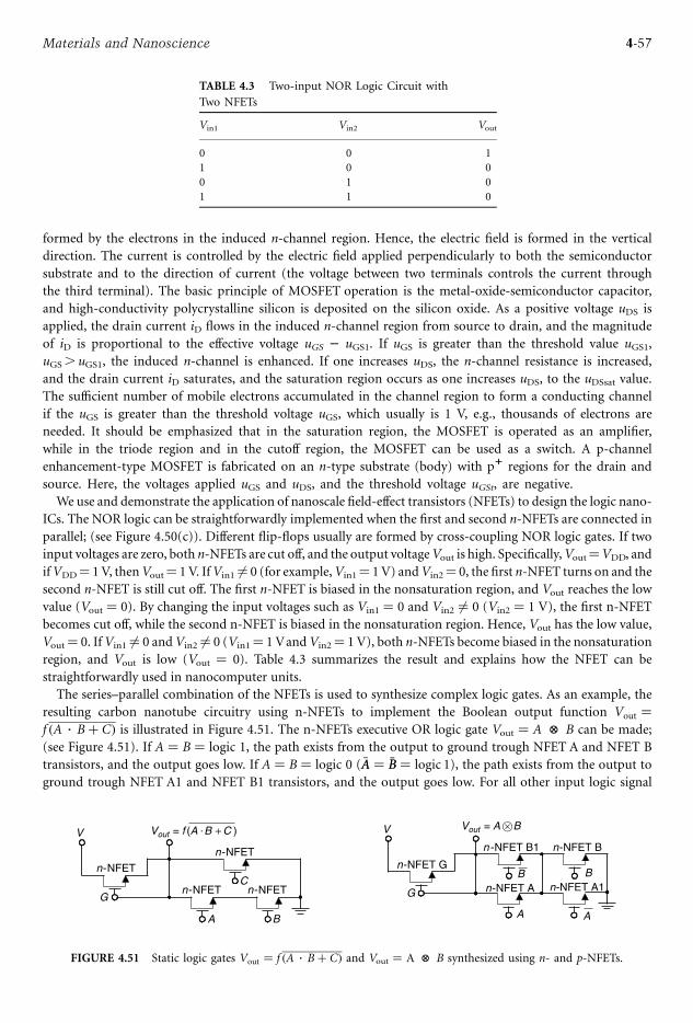
formed by the electrons in the induced n-channel region. Hence, the electric field is formed in the vertical
direction. The current is controlled by the electric field applied perpendicularly to both the semiconductor
substrate and to the direction of current (the voltage between two terminals controls the current through
the third terminal). The basic principle of MOSFET operation is the metal-oxide-semiconductor capacitor,
and high-conductivity polycrystalline silicon is deposited on the silicon oxide. As a positive voltage uDS is
applied, the drain current iD flows in the induced n-channel region from source to drain, and the magnitude
of iD is proportional to the effective voltage uGS uGS1. If uGS is greater than the threshold value uGS1,
uGS. uGS1, the induced n-channel is enhanced. If one increases uDS, the n-channel resistance is increased,
and the drain current iD saturates, and the saturation region occurs as one increases uDS, to the uDSsat value.
The sufficient number of mobile electrons accumulated in the channel region to form a conducting channel
if the uGS is greater than the threshold voltage uGS, which usually is 1 V, e.g., thousands of electrons are
needed. It should be emphasized that in the saturation region, the MOSFET is operated as an amplifier,
while in the triode region and in the cutoff region, the MOSFET can be used as a switch. A p-channel
enhancement-type MOSFET is fabricated on an n-type substrate (body) with p1 regions for the drain and
source. Here, the voltages applied uGS and uDS, and the threshold voltage uGSt, are negative.
We use and demonstrate the application of nanoscale field-effect transistors (NFETs) to design the logic nano-
ICs. The NOR logic can be straightforwardly implemented when the first and second n-NFETs are connected in
parallel; (see Figure 4.50(c)). Different flip-flops usually are formed by cross-coupling NOR logic gates. If two
input voltages are zero, both n-NFETs are cut off, and the output voltageVout is high. Specifically,Vout¼VDD, and
ifVDD¼ 1 V, thenVout¼ 1 V. IfVin1 6¼ 0 (for example,Vin1¼ 1 V) andVin2¼ 0, the first n-NFET turns on and the
second n-NFET is still cut off. The first n-NFET is biased in the nonsaturation region, and Vout reaches the low
value (Vout ¼ 0). By changing the input voltages such as Vin1 ¼ 0 and Vin2 6¼ 0 (Vin2 ¼ 1 V), the first n-NFET
becomes cut off, while the second n-NFET is biased in the nonsaturation region. Hence, Vout has the low value,
Vout¼ 0. IfVin1 6¼ 0 andVin2 6¼ 0 (Vin1¼ 1 VandVin2¼ 1 V), both n-NFETs become biased in the nonsaturation
region, and Vout is low (Vout ¼ 0). Table 4.3 summarizes the result and explains how the NFET can be
straightforwardly used in nanocomputer units.
The series–parallel combination of the NFETs is used to synthesize complex logic gates. As an example, the
resulting carbon nanotube circuitry using n-NFETs to implement the Boolean output function Vout ¼f ðA Bþ CÞ is illustrated in Figure 4.51. The n-NFETs executive OR logic gate Vout ¼ A B can be made;
(see Figure 4.51). If A ¼ B ¼ logic 1, the path exists from the output to ground trough NFET A and NFET B
transistors, and the output goes low. If A ¼ B ¼ logic 0 (AA ¼ BB ¼ logic 1), the path exists from the output to
ground trough NFET A1 and NFET B1 transistors, and the output goes low. For all other input logic signal
TABLE 4.3 Two-input NOR Logic Circuit with
Two NFETs
Vin1 Vin2 Vout
0 0 1
1 0 0
0 1 0
1 1 0
V
A
C
G
n-NFET
n-NFET
V
A
n-NFET A1G
n-NFET G
n -NFET B1
B
A
B
n-NFET B
n-NFET A
Vout = f (A .B + C )
n-NFET n-NFET
B
Vout = A B
FIGURE 4.51 Static logic gates Vout ¼ f ðA Bþ CÞ and Vout ¼ A B synthesized using n- and p-NFETs.
4-57Materials and Nanoscience
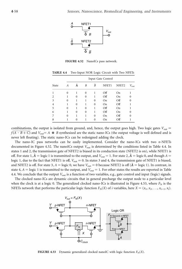
combinations, the output is isolated from ground, and, hence, the output goes high. Two logic gates Vout ¼f ðA Bþ CÞ and Vout¼ A B synthesized are the static nano-ICs (the output voltage is well defined and is
never left floating). The static nano-ICs can be redesigned adding the clock.
The nano-IC pass networks can be easily implemented. Consider the nano-ICs with two n-NFETs
documented in Figure 4.52. The nanoICs output Vout is determined by the conditions listed in Table 4.4. In
states 1 and 2, the transmission gate of NFET2 is biased in its conduction state (NFET2 is on), while NFET1 is
off. For state 1, AA ¼ logic 1 is transmitted to the output, and Vout ¼ 1. For state 2, AA ¼ logic 0, and though A¼logic 1, due to the fact that NFET1 is off, Vout ¼ 0. In states 3 and 4, the transmission gate of NFET1 is biased,
and NFET2 is off. For state 3, A ¼ logic 0, we have Vout ¼ 0 because NFET2 is off (AA ¼ logic 1). In contrast, in
state 4, A ¼ logic 1 is transmitted to the output, and Vout ¼ 1. For other states the results are reported in Table
4.4. We conclude that the output Vout is a function of two variables, e.g., gate control and input (logic) signals.
The clocked nano-ICs are dynamic circuits that in general precharge the output node to a particular level
when the clock is at a logic 0. The generalized clocked nano-ICs is illustrated in Figure 4.53, where FN is the
NFETs network that performs the particular logic function FN(X) of i variables, here X ¼ (x1, x2, . . ., xi 1, xi).
TABLE 4.4 Two-Input NOR Logic Circuit with Two NFETs
Input Gate Control
State A AA B B NFET1 NFET2 Vout
1 0 1 0 1 Off On 1
2 1 0 0 1 Off On 0
3 0 1 1 0 On Off 0
4 1 0 1 0 On Off 1
5 0 1 0 1 Off On 1
6 1 0 0 1 Off On 0
7 0 1 1 0 On Off 0
8 1 0 1 0 On Off 1
V n-NFETNF
X
Cclock
p -NFETV
Vout = FN(X )
FN Second n-NFET
First n -NFET
A
B
Logic OR
p-NFET
n -NFET
FIGURE 4.53 Dynamic generalized clocked nanoIC with logic function FN(X).
A NFET1
B
A
B
NFET2
Vout
FIGURE 4.52 NanoICs pass network.
4-58 Sensors, Nanoscience, Biomedical Engineering, and Instruments
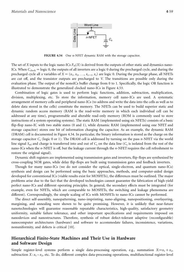
The set of X inputs to the logic nano-ICs FN(X) is derived from the outputs of other static and dynamics nano-
ICs. When Cclock ¼ logic 0, the outputs of all inverters are a logic 0 during the precharged cycle, and during the
precharged cycle all x variables of X ¼ (x1, x2, . . ., xz 1, xz) are logic 0. During the precharge phase, all NFETs
are cut off, and the transistor outputs are precharged to V. The transitions are possible only during the
evaluation phase. The output of the nonoICs buffer change from 0 to 1. Specifically, the logic OR function is
illustrated to demonstrate the generalized clocked nano-ICs in Figure 4.53.
Combination of logic gates is used to perform logic functions, addition, subtraction, multiplication,
division, multiplexing, etc. To store the information, memory cell nano-ICs are used. A systematic
arrangement of memory cells and peripheral nano-ICs (to address and write the data into the cells as well as to
delete data stored in the cells) constitute the memory. The NFETs can be used to build superior static and
dynamic random access memory (RAM is the read-write memory in which each individual cell can be
addressed at any time), programmable and alterable read-only memory (ROM is commonly used to store
instructions of a system operating systems). The static RAM (implemented using six NFETs) consists of a basic
flip-flop nano-IC with two stable states (0 and 1), while dynamic RAM (implemented using one NFET and
storage capacitor) stores one bit of information charging the capacitor. As an example, the dynamic RAM
(DRAM) cell is documented in Figure 4.54. In particular, the binary information is stored as the charge on the
storage capacitor Cs (logic 0 or 1). The DRAM cell is addressed by turning on the pass n-NFET via the world
line signal Swl and charge is transferred into and out of Cs on the data line (Cs is isolated from the rest of the
nano-ICs when the n-NFET is off, but the leakage current through the n-NFET requires the cell refreshment to
restore the original signal).
Dynamic shift registers are implemented using transmission gates and inverters, flip-flops are synthesized by
cross-coupling NOR gates, while delay flip-flops are built using transmission gates and feedback inverters.
Though for many nano-ICs (we do not consider the optical, single-electron, and quantum nano-ICs)
synthesis and design can be performed using the basic approaches, methods, and computer-aided design
developed for conventional ICs (viable results exist for MOSFETs), the differences must be outlined. The major
problems arise due to the fact that the developed technologies cannot guarantee the fabrication of high-yield
perfect nano-ICs and different operating principles. In general, the secondary effects must be integrated (for
example, even for NFETs, which are comparable to MOSFETs, the switching and leakage phenomena are
different). Correspondingly, the simple scaling of ICs with MOSFETs to nano-ICs cannot be performed.
The direct self-assembly, nanopatterning, nano-imprinting, nano-aligning, nanopositioning, overlayering,
margining, and annealing were shown to be quite promising. However, it is unlikely that near-future
nanotechnologies will guarantee reasonable repeatable characteristics, high-quality, satisfactory geometry
uniformity, suitable failure tolerance, and other important specifications and requirements imposed on
nanodevices and nanostructures. Therefore, synthesis of robust defect-tolerant adaptive (reconfigurable)
nanocomputer architectures (hardware) and software to accommodate failures, inconsistence, variations,
nonuniformity, and defects is critical [10].
Hierarchical Finite-State Machines and Their Use in Hardwareand Software Design
Simple register-level systems perform a single data-processing operation, e.g., summation X:¼x1þ x2,
subtraction X : x1 – x2, etc. To do, different complex data-processing operations, multifunctional register-level
Cs
Word Line
n-NFET
Dat
aLi
ne
FIGURE 4.54 One n-NFET dynamic RAM with the storage capacitor.
4-59Materials and Nanoscience
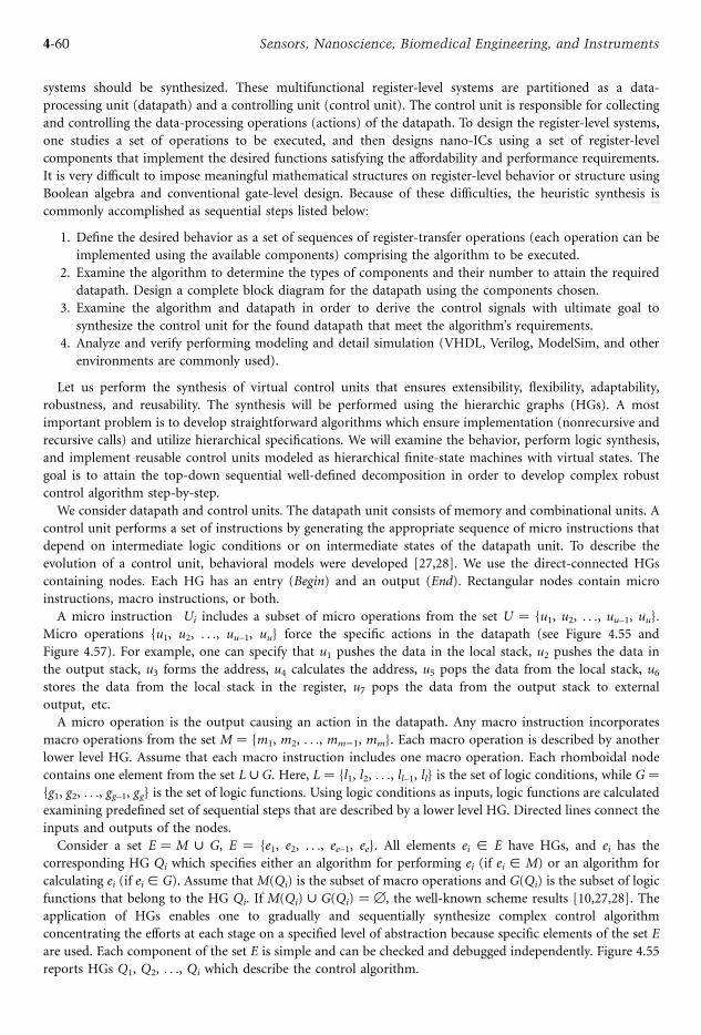
systems should be synthesized. These multifunctional register-level systems are partitioned as a data-
processing unit (datapath) and a controlling unit (control unit). The control unit is responsible for collecting
and controlling the data-processing operations (actions) of the datapath. To design the register-level systems,
one studies a set of operations to be executed, and then designs nano-ICs using a set of register-level
components that implement the desired functions satisfying the affordability and performance requirements.
It is very difficult to impose meaningful mathematical structures on register-level behavior or structure using
Boolean algebra and conventional gate-level design. Because of these difficulties, the heuristic synthesis is
commonly accomplished as sequential steps listed below:
1. Define the desired behavior as a set of sequences of register-transfer operations (each operation can be
implemented using the available components) comprising the algorithm to be executed.
2. Examine the algorithm to determine the types of components and their number to attain the required
datapath. Design a complete block diagram for the datapath using the components chosen.
3. Examine the algorithm and datapath in order to derive the control signals with ultimate goal to
synthesize the control unit for the found datapath that meet the algorithm’s requirements.
4. Analyze and verify performing modeling and detail simulation (VHDL, Verilog, ModelSim, and other
environments are commonly used).
Let us perform the synthesis of virtual control units that ensures extensibility, flexibility, adaptability,
robustness, and reusability. The synthesis will be performed using the hierarchic graphs (HGs). A most
important problem is to develop straightforward algorithms which ensure implementation (nonrecursive and
recursive calls) and utilize hierarchical specifications. We will examine the behavior, perform logic synthesis,
and implement reusable control units modeled as hierarchical finite-state machines with virtual states. The
goal is to attain the top-down sequential well-defined decomposition in order to develop complex robust
control algorithm step-by-step.
We consider datapath and control units. The datapath unit consists of memory and combinational units. A
control unit performs a set of instructions by generating the appropriate sequence of micro instructions that
depend on intermediate logic conditions or on intermediate states of the datapath unit. To describe the
evolution of a control unit, behavioral models were developed [27,28]. We use the direct-connected HGs
containing nodes. Each HG has an entry (Begin) and an output (End). Rectangular nodes contain micro
instructions, macro instructions, or both.
A micro instruction Ui includes a subset of micro operations from the set U ¼ u1, u2, . . ., uu–1, uu.
Micro operations u1, u2, . . ., uu–1, uu force the specific actions in the datapath (see Figure 4.55 and
Figure 4.57). For example, one can specify that u1 pushes the data in the local stack, u2 pushes the data in
the output stack, u3 forms the address, u4 calculates the address, u5 pops the data from the local stack, u6stores the data from the local stack in the register, u7 pops the data from the output stack to external
output, etc.
A micro operation is the output causing an action in the datapath. Any macro instruction incorporates
macro operations from the set M ¼ m1, m2, . . ., mm 1, mm. Each macro operation is described by another
lower level HG. Assume that each macro instruction includes one macro operation. Each rhomboidal node
contains one element from the set L [ G. Here, L ¼ l1, l2, . . ., ll–1, ll is the set of logic conditions, while G ¼g1, g2, . . ., gg–1, gg is the set of logic functions. Using logic conditions as inputs, logic functions are calculated
examining predefined set of sequential steps that are described by a lower level HG. Directed lines connect the
inputs and outputs of the nodes.
Consider a set E ¼ M [ G, E ¼ e1, e2, . . ., ee–1, ee. All elements ei [ E have HGs, and ei has the
corresponding HG Qi which specifies either an algorithm for performing ei (if ei [ M) or an algorithm for
calculating ei (if ei [ G). Assume thatM(Qi) is the subset of macro operations and G(Qi) is the subset of logic
functions that belong to the HG Qi. If M(Qi) [ G(Qi) ¼ B, the well-known scheme results [10,27,28]. The
application of HGs enables one to gradually and sequentially synthesize complex control algorithm
concentrating the efforts at each stage on a specified level of abstraction because specific elements of the set E
are used. Each component of the set E is simple and can be checked and debugged independently. Figure 4.55
reports HGs Q1, Q2, . . ., Qi which describe the control algorithm.
4-60 Sensors, Nanoscience, Biomedical Engineering, and Instruments
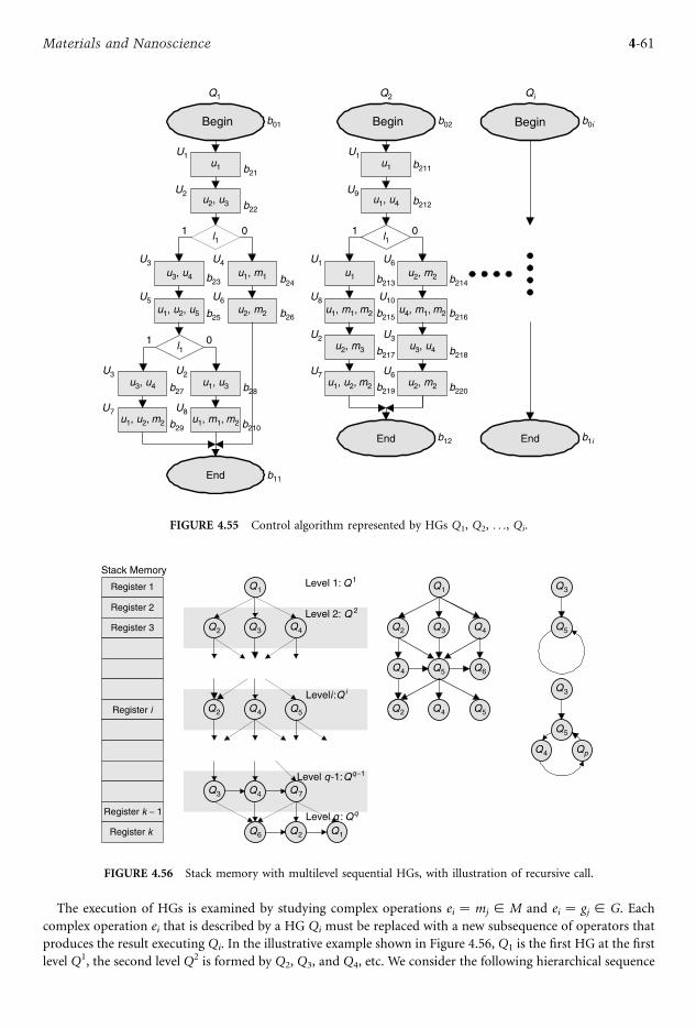
The execution of HGs is examined by studying complex operations ei ¼ mj [ M and ei ¼ gj [ G. Each
complex operation ei that is described by a HG Qi must be replaced with a new subsequence of operators that
produces the result executing Qi. In the illustrative example shown in Figure 4.56, Q1 is the first HG at the first
level Q1, the second level Q2 is formed by Q2, Q3, and Q4, etc. We consider the following hierarchical sequence
Register 1
Register 2
Register 3
Register i
Register k − 1
Register k
Q1Level 1: Q 1
Level 2: Q 2
Leveli :Q i
Level q : Qq
Level q-1:Qq−1
Stack Memory
Q2
Q2
Q3
Q6
Q2 Q3
Q3
Q4
Q5
Q7Q4
Q4 Q2 Q5Q4
Q5
Q5
Q6Q4
Q1
Q1 Q3
Q5
Q4 Qp
Q2 Q3 Q4
FIGURE 4.56 Stack memory with multilevel sequential HGs, with illustration of recursive call.
u1
Begin
l11
End
Q1 Q2 Qi
b21b211
b22b212
U1 U1
U2 U9
Begin
End
Begin
End
b01 b02 b0i
b1i
u2, u3 u1, u4
u2, m2
u2, m2
u2, m3 u3, u4
u2, m2
0 1 0
u1, u2, m2 u1, m1, m2
u1, m1, m2
u1, u2, m2
u4, m1, m2u1, u2, u5
u3, u4
u3, u4 u1, u3
u1, m1
b217
U3
U3
U7
U4 U1 U6
U2
U8
U6U5 U10U8
U2
U7 U6
U3
b26
b11
b12
b25 b215 b216
b218
b220b219b27
b29
b28
b210
b24 b214b23 b213
l11 0
u1
l1
u1
FIGURE 4.55 Control algorithm represented by HGs Q1, Q2, . . ., Qi.
4-61Materials and Nanoscience

of HGs Q1 ðlevel 1Þ ) Q2ðlevel 2Þ ) ) Qq 1 ðlevel q 1Þ ) Qq ðlevel qÞ. All Qi (level i) have the corresponding HGs.
For example, Q2 is a subset of the HGs that are used to describe elements from the set M(Q1) [ G(Q1) ¼ B,
while Q3 is a subset of the HGs that are used to map elements from the sets [ q2Q2 MðqÞ and [ q2Q2 GðqÞ.In Figure 4.56, Q1 ¼ Q1, Q
2 ¼ Q2, Q3, Q4, Q3 ¼ Q2, Q4, Q5, etc.
Micro operations u1 and u– are used to increment and to decrement the stack pointer (SP). The problem of
switching to various levels can be solved using a stack memory, see Figure 4.56. Consider an algorithm for ei[
M(Q1) [ G(Q1) ¼ B. The SP is incremented by the micro operation u+, and a new register of the stack
memory is set as the current register. The previous register stores the state when it was interrupted. New Qi
becomes responsible for the control until terminated. After termination of Qi, the micro operation u is
generated to return to the interrupted state. As a result, control is passed to the state in which Qf is called.
The synthesis problem can be formulated as: for a given control algorithm A, described by the set of HGs,
construct the FSM that implements A.
In general, the synthesis includes the following steps:
. transforming the HGs to the state transition table
. state encoding
. combinational logic optimization
. final structure design
The first step is divided into substeps as: (1) marking the HGs with labels b (see Figure 4.56); (2) recording
all transitions between the labels in the extended state transition table; and (3) convert the extended table to
ordinary form.
The labels b01 and b11 are assigned to the nodes Begin and End of the Q1. The label b02, . . ., b0i and b12, . . .,
b1i are assigned to nodes Begin and End of Q2, . . ., Qi, respectively. The labels b21, b22, . . ., b2j are assigned to
other nodes of HGs, inputs and outputs of nodes with logic conditions, etc. Repeating labels are not allowed.
The labels are considered as the states. The extended state transition table is designed using the state evolutions
due to inputs (logic conditions) and logic functions, which cause the transitions from x(t) to x(t + 1). All
evolutions of the state vector x(t) are recorded, and the state xk(t) has the label k. It should be emphasized that
the table can be converted from the extended to the ordinary form. To program the Code Converter, one
records the transition from the state x1 assigned to the Begin node of the HG Q1, e.g., x01 ) x21ðQ1Þ. Thetransitions between different HGs are recorded as xi;j ) xn;mðQjÞ. For all transitions, the data-transfer
instructions are synthesized. The hardware implementation is illustrated in Figure 4.57.
LocalStack
OutputData
ul
u +, u −
ursT
rcControl NanoICs
Mout
Min
u u
T
StackMemory
Clock
Code Converter
OutputStack
RAM
Register
CombinationalNanoICs
FIGURE 4.57 Hardware implementation.
4-62 Sensors, Nanoscience, Biomedical Engineering, and Instruments
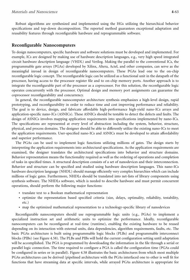
Robust algorithms are synthesized and implemented using the HGs utilizing the hierarchical behavior
specifications and top-down decomposition. The reported method guarantees exceptional adaptation and
reusability features through reconfigurable hardware and reprogrammable software.
Reconfigurable Nanocomputers
To design nanocomputers, specific hardware and software solutions must be developed and implemented. For
example, ICs are designed by making use of hardware description languages, e.g., very high speed integrated
circuit hardware description language (VHDL) and Verilog. Making the parallel to the conventional ICs, the
programmable gate arrays (PGAs) developed by Xilinx, Altera, Actel, and other companies, can serve as the
meaningful inroad in design of reconfigurable nanocomputers. These PGAs lead one to the on-chip
reconfigurable logic concept. The reconfigurable logic can be utilized as a functional unit in the datapath of the
processor, having access to the processor register file and to on-chip memory ports. Another approach is to
integrate the reconfigurable part of the processor as a coprocessor. For this solution, the reconfigurable logic
operates concurrently with the processor. Optimal design and memory port assignments can guarantee the
coprocessor reconfigurability and concurrency.
In general, the reconfigurable nanocomputer architecture synthesis emphasizes a high-level design, rapid
prototyping, and reconfigurability in order to reduce time and cost improving performance and reliability.
The goal is to device, design, and fabricate affordable high-performance high-yield nano-ICs arrays and
application-specific nano-ICs (ASNICs). These ASNICs should be testable to detect the defects and faults. The
design of ASNICs involves mapping application requirements into specifications implemented by nano-ICs.
The specifications are represented at every level of abstraction including the system, behavior, structure,
physical, and process domains. The designer should be able to differently utilize the existing nano-ICs to meet
the application requirements. User-specified nano-ICs and ASNICs must be developed to attain affordability
and superior performance.
The PGAs can be used to implement logic functions utilizing millions of gates. The design starts by
interpreting the application requirements into architectural specifications. As the application requirements are
examined, the designer translates the architectural specifications into behavior and structure domains.
Behavior representation means the functionality required as well as the ordering of operations and completion
of tasks in specified times. A structural description consists of a set of nanodevices and their interconnection.
Behavior and structure can be specified and studied using hardware description languages. This nano-ICs
hardware description language (NHDL) should manage efficiently very complex hierarchies which can include
millions of logic gates. Furthermore, NHDLs should be translated into net-lists of library components using
synthesis software. The NHDLs software, which is needed to describe hardware and must permit concurrent
operations, should perform the following major functions:
. translate text to a Boolean mathematical representation
. optimize the representation based specified criteria (size, delays, optimality, reliability, testability,
etc.). map the optimized mathematical representation to a technology-specific library of nanodevices
Reconfigurable nanocomputers should use reprogrammable logic units (e.g., PGAs) to implement a
specialized instruction set and arithmetic units to optimize the performance. Ideally, reconfigurable
nanocomputers can be reconfigured at real-time (runtime), enabling the existing hardware to be reused
depending on its interaction with external units, data dependencies, algorithm requirements, faults, etc. The
basic PGAs architecture is built using programmable logic blocks (PLBs) and programmable interconnect
blocks (PIBs) (see Figure 4.58). The PLBs and PIBs will hold the current configuration setting until adaptation
will be accomplished. The PGA is programmed by downloading the information in the file through a serial or
parallel logic connection. The time required to configure a PGA is called the configuration time (PGAs could
be configured in series or in parallel). Figure 4.58 illustrates the basic architectures from which most multiple
PGAs architectures can be derived (pipelined architecture with the PGAs interfaced one to other is well fit for
functions that have streaming data at specific intervals, while arrayed PGAs architecture is appropriate for
4-63Materials and Nanoscience
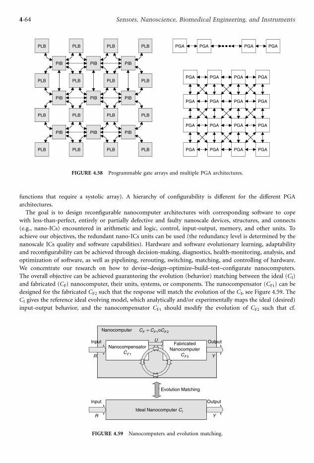
functions that require a systolic array). A hierarchy of configurability is different for the different PGA
architectures.
The goal is to design reconfigurable nanocomputer architectures with corresponding software to cope
with less-than-perfect, entirely or partially defective and faulty nanoscale devices, structures, and connects
(e.g., nano-ICs) encountered in arithmetic and logic, control, input-output, memory, and other units. To
achieve our objectives, the redundant nano-ICs units can be used (the redundancy level is determined by the
nanoscale ICs quality and software capabilities). Hardware and software evolutionary learning, adaptability
and reconfigurability can be achieved through decision-making, diagnostics, health-monitoring, analysis, and
optimization of software, as well as pipelining, rerouting, switching, matching, and controlling of hardware.
We concentrate our research on how to devise–design–optimize–build–test–configurate nanocomputers.
The overall objective can be achieved guaranteeing the evolution (behavior) matching between the ideal (CI)
and fabricated (CF) nanocomputer, their units, systems, or components. The nanocompensator (CF1) can be
designed for the fabricated CF2 such that the response will match the evolution of the CI, see Figure 4.59. The
CI gives the reference ideal evolving model, which analytically and/or experimentally maps the ideal (desired)
input-output behavior, and the nanocompensator CF1 should modify the evolution of CF2 such that cf.
Input
Evolution Matching
Nanocomputer
FabricatedNanocomputer
CF 2
CF = CF 1oCF 2
OutputNanocompensator
CF 1
Input
Ideal Nanocomputer CI
Output
R
Y
Y
U
R
FIGURE 4.59 Nanocomputers and evolution matching.
PLB
PIB
PLB PLB
PIB
PLB
PIB
PLB
PIB
PLB PLB
PIB
PLB
PIB
PLB PLB PLB PLB
PGA PGA
PIB PIBPIB
PLB PLB PLB PLB
PGAPGA
PGA PGAPGAPGA
PGA PGAPGAPGA
PGA PGAPGAPGA
PGA PGAPGAPGA
FIGURE 4.58 Programmable gate arrays and multiple PGA architectures.
4-64 Sensors, Nanoscience, Biomedical Engineering, and Instruments

described by CF ¼ CF1 CF2 (series architecture), matches the CI behavior. Figure 4.59 illustrates the concept.
The necessary and sufficient conditions for strong and weak evolution matching based on CI and CF2 must be
derived.
Mathematical Models for Nanocomputers
Sixtuple Nanocomputer Model
To address analysis, control, diagnostics, optimization, and design problems, the explicit mathematical models
of nanocomputers must be developed and applied. There are different levels of abstraction in nanocomputer
modeling, simulation, and analysis [10]. High-level models can accept streams of instruction descriptions and
memory references, while the low-level (device-level) logic gates or memory modeling can be performed by
making use of streams of input and output signals and nonlinear transient behavior of devices. The system-
and subsystem-level modeling (medium-level) also can be formulated and performed. It is evident that one
subsystem can contain millions of nanodevices. For example, computer systems can be modeled as queuing
networks. Different mathematical modeling frameworks exist and have been developed for each level. In this
section we concentrate on the high-, medium-, and low-level systems modeling of nanocomputer systems
using the finite state machine concept.
The computer accepts the input information, processes it according to the stored instructions, and produces
the output. There exist numerous computer models, e.g., Boolean models, polynomial models, information-
based, etc. However, all mathematical models are the mathematical idealization based upon the abstractions,
simplifications and hypotheses made. In fact, it is virtually impossible to develop and apply the complete
mathematical model due to complexity and numerous obstacles.
It is possible to concurrently model nanocomputers by the sixtuple:
C ¼ fX; E;R;Y; F;X0g
where X is the finite set of states with initial and final states x0 [ X and xf # X; E is the finite set of events
(concatenation of events forms a string of events); R and Y are the finite sets of the input and output symbols
(alphabets); F are the transition functions mapping from X6 E6 R6 Y to X (denoted as FX), to E (denoted
as FE) or to Y (denoted as FY), F # X 6 E 6 R 6 Y (we assume that F ¼ FX, e.g., the transition function
defines a new state to each quadruple of states, events, references, and outputs, and F can be represented by a
table listing the transitions or by a state diagram).
The nanocomputer evolution is due to inputs, events, state evolutions, and parameter variations (as
explained at the end of this subsection), etc.
We formulate two useful definitions.
Definition 1. A vocabulary (or an alphabet) A is a finite nonempty set of symbols (elements). A world (or
sentence) over A is a string of finite length of elements of A. The empty (null) string is the string which does
not contain symbols. The set of all words over A is denoted as Aw. A language over A is a subset of Aw.
Definition 2. A finite-state machine with outputCFS¼ X,AR,AY, FR, FY,X0 consists of a finite set of states S, a
finite input alphabetAR, a finite output alphabetAY, a transition function FY that assigns a new state to each state
and input pair, an output function FY that assigns an output to each state and input pair, and initial state X0.
Using the input-output map, the evolution of C can be expressed as
Ec R Y
That is, if the computer in state x [ X receives an input r [ R, it moves to the next state f(x, r) and produces
the output y(x, r). Nanocomputers can be represented as the state tables that describe the state and output
functions. In addition, the state transition diagram (direct graph whose vertices correspond to the states and
edges correspond to the state transitions, and each edge is labeled with the input and output associated with
the transition) is frequently used.
4-65Materials and Nanoscience

Nanocomputer Modeling with Parameters Set
Nanocomputers can be modeled using the parameters set P. Designing reconfigurable fault-tolerant
nanocomputer architectures, sets P and P0 should be integrated, and we have
C ¼ fX; E;R;Y;P; F;X0;P0g:It is evident that nanocomputer evolution depends upon P and P0. The optimal performance can be achieved
through adaptive synthesis, reconfiguration and diagnostics. For example, one can vary F and variable
parameters Pv to attain the best possible performance.
Nanocomputer evolution, considering states, events, outputs, and parameters, can be expressed as
ðx0;e0;y0;p0Þ )evolution1 ðx1;e1;y1;p1Þ )evolution2 )evolution j 1 ðxj 1;ej 1;yj 1;pj 1Þ )evolution j ðxj;ej;yj;pjÞ:
The input, states, outputs, events, and parameter sequences are aggregated within the model C¼ X, E, R, Y, P,
F, X0, P0. The concept reported allows us to find and apply the minimal, but complete functional description
of nanocomputers. The minimal subset of state, event, output, and parameter evolutions (transitions) can be
used. That is, the partial description Cpartial, C results, and every essential nanocomputer quadruple (xi, ei, yi,
pi) can be mapped by (xi, ei, yi, pi)partial. This significantly reduces the complexity modeling, simulation,
analysis, and design problems.
Let the transition function Fmap from X6 E6 R6 Y6 P to X, e.g., F: X6 E6 R6 Y6 P! X, F#
X6 E6 R6 Y6 P. Thus, the transfer function F defines a next state x(t þ 1) [ X based upon the current
state x(t) [ X, event e(t) [ E, reference r(t) [ R, output y(t) [ Y and parameter p(t) [ P. Hence:
xðt þ 1Þ ¼ F xðtÞ; eðtÞ; rðtÞ; yðtÞ; pðtÞ for x0ðtÞ 2 X0 and p0ðtÞ 2 P0:
The robust adaptive control algorithms must be developed. The control vector u(t) [ U is integrated into the
nanocomputer model. We have C ¼ X, E, R, Y, P, U, F, X0, P0.
The nanocompensator synthesis procedure is reported in the following sections. This synthesis approach is
directly applicable to design nanocomputers with two- and three-dimensional nano-ICs.
Nanocompensator Synthesis and Design Aspects
In this section we will design the nanocompensator. Two useful definitions that allow one to precisely
formulate and solve the problem are formulated.
Definition 3. The strong evolutionary matching CF ¼ CF1 CF2 ¼ BCI for given CI and CF is guaranteed if
ECF ¼ EC1. Here, CF¼ B C1 means that the behaviors (evolution) of CI and CF are equivalent.
Definition 4. The weak evolutionary matching CF ¼ CF1 CF2 # BC1 for given CI and CF is guaranteed if ECF
# EC1. Here, CF # BC1 means that the evolution of CF is contained in the behavior CI.
The problem is to derive a nanocompensator CF1 ¼XF1, EF1, RF1, YF1, FF1, XF10 such that for given
C1 ¼ X1, E1, R1, Y1, F1, X10 and CF2 ¼XF2, EF2, RF2, YF1, FF2, XF20 the following conditions:
CF ¼ CF1 CF2 ¼BCI ðstrong behavior matchingÞor
CF ¼ CF1 CF2 BCI ðweak behavior matchingÞare satisfied.
Here, we assume that the following conditions are satisfied:
. output sequences generated by CI can be generated by CF2
. the CI inputs match the CF1 inputs
4-66 Sensors, Nanoscience, Biomedical Engineering, and Instruments

It must be emphasized that the output sequence means the state, event, output, and/or parameters vectors,
e.g., the triple (x, e, y, p).
Lemma 1. If there exists the state-modeling representation g # X1 6 XF such that C 1I
gBC
1F2 (if
C 1I
gBC
1F2 , then CI
gBCF2), then the evolution matching problem is solvable. The nanocompensator CF1
solves the strong matching problem CF ¼ CF1 CF2 ¼ BC1 if there exist the state-modeling representations
b # X1 6 XF2, (X10, XF20,) [ b and a # XF1 6 b, (XF10, (X10, XF20)) [ a such that CF1 ¼ aBC
b1 for
b 2 G ¼ fgjC 1I
gBC
1F2 g. Furthermore, the strong matching problem is tractable if there exist C 1
I and C 1F2 .
The nanocomputer can be decomposed using algebraic decomposition theory, which is based on the
closed partition lattice. For example, consider the fabricated nanocomputer CF2 represented as CF2 ¼ XF2,
EF2, RF2, YF2, XF20.
A partition on the state set for CF2 is a set CF2 1, CF2 2, . . . CF2 i, . . . CF2 k–1, CF2 k of disjoint subsets of the
state set XF2 whose union is XF2, e.g.,Ski¼1
CF2i ¼ XF2 and CF2iTCF2j ¼ ; for i 6¼ j. Hence, we can design and
implement the nanocompensators (hardware) CF1 i for given CF2 i.
References
1. J. Appenzeller, R. Martel, P. Solomon, K. Chan, P. Avouris, J. Knoch, J. Benedict, M. Tanner, S. Thomas,
L.L. Wang, and J.A. Del Alamo, ‘‘A 10 nm MOSFET concept,’’ Microelectronic Engineering, vol. 56,
no. 1–2, pp. 213–219, 2001.
2. Y. Chen, D.A.A. Ohlberg, G. Medeiros-Ribeiro, Y.A. Chang, and R.S. Williams, ‘‘Self-assembled growth of
epitaxial erbium disilicide nanowires on silicon (001),’’ Appl. Phys. Lett., vol. 76, pp. 4004–4006, 2000.
3. V. Derycke, R. Martel. J. Appenzeller, and P. Avouris, ‘‘Carbon nanotube inter- and inramolecular logic
gates,’’ Nano Lett., 2001.
4. J.C. Ellenbogen and J.C. Love, ‘‘Architectures for molecular electronic computers: Logic structures and
an adder designed from molecular electronic diodes,’’ Proc. IEEE, vol. 88, no. 3, pp. 386–426, 2000.
5. W.L. Henstrom, C.P. Liu, J.M. Gibson, T.I. Kamins, and R.S. Williams, ‘‘Dome-to-pyramid shape
transition in Ge/Si islands due to strain relaxation by interdiffusion,’’ Appl. Phys. Lett., vol. 77,
pp. 1623–1625, 2000.
6. S.C. Goldstein, ‘‘Electronic nanotechnology and reconfigurable computing,’’ Proc. Computer Society
Workshop on VLSI, pp. 10–15, 2001.
7. T.I. Kamins and D.P. Basile, ‘‘Interaction of self-assembled Ge islands and adjacent Si layers grown on
unpatterned and patterned Si (001) substrates,’’ J. Electronic Materials, vol. 29, pp. 570–575, 2000.
8. T.I. Kamins, R.S. Williams, Y. Chen, Y.L. Chang, and Y.A. Chang, ‘‘Chemical vapor deposition of Si
nanowires nucleated by TiSi2 islands on Si,’’ Appl. Phys. Lett., vol. 76, pp. 562–564, 2000.
9. T.I. Kamins, R.S. Williams, D.P. Basile, T. Hesjedal, and J.S. Harris, ‘‘Ti-catalyzed Si nanowires by
chemical vapor deposition: Microscopy and growth mechanism,’’ J. Appl. Phys., vol. 89, pp. 1008–1016,
2001.
10. S.E. Lyshevski, Nanocomputer architectronics and nanotechnology, in Handbook of Nano-science,
Engineering, and Technology, Eds W.A. Goddard, D.W. Brenner, S.E. Lyshevski, and G.J. Iafrate, Boca
Raton, FL: CRC Press, pp. 6-1 to 6-38, 2003.
11. R. Martel, H.S.P. Wong, K. Chan, and P. Avouris, ‘‘Carbon nanotube field effect transistors for logic
applications,’’ Proc. Electron Devices Meeting, IEDM Technical Digest, pp. 7.5.1–7.5.4, 2001.
12. P.L. McEuen, J. Park, A. Bachtold, M. Woodside, M.S. Fuhrer, M. Bockrath, L. Shi, A. Majumdar, and
P. Kim, ‘‘Nanotube nanoelectronics,’’ Proc. Device Research Conf., pp. 107–110, 2001.
13. R. Saito, G. Dresselhaus and M.S. Dresselhaus, Physical Properties of Carbon Nanotubes, London:
Imperial College Press, 1999.
14. W.T. Tian, S. Datta, S. Hong, R. Reifenberger, J.I. Henderson, and C.P. Kubiak, ‘‘Conductance spectra of
molecular wires,’’ Int. J. Chemical Physics, vol. 109, no. 7, pp. 2874–2882, 1998.
15. K. Tsukagoshia, A. Kanda, N. Yoneya, E. Watanabe, Y. Ootukab, and Y. Aoyagi, ‘‘Nano-electronics in a
multiwall carbon nanotube,’’ Proc. Microprocesses and Nanotechnology Conf., pp. 280–281, 2001.
4-67Materials and Nanoscience

16. E.K. Drexler, Nanosystems: Molecular Machinery, Manufacturing, and Computations,Wiley-Interscience,
New York, 1992.
17. J. Carter, Microprocessor Architecture and Microprogramming, a State Machine Approach, Prentice-Hall,
Englewood Cliffs, NJ, 1996.
18. V.C. Hamacher, Z.G. Vranesic, and S.G. Zaky, Computer Organization, McGraw-Hill, New York, 1996.
19. J.P. Hayes, Computer Architecture and Organizations, McGraw-Hill, Boston, MA, 1998.
20. J.L. Hennessy and D.A. Patterson, Computer Architecture: A Quantitative Approach, Morgan Kaufman,
San Mateo, CA, 1990.
21. K. Hwang, Computer Arithmetic, Wiley, New York, 1978.
22. K. Likharev, ‘‘Riding the crest of a new wave in memory,’’ IEEE Circuits and Devices Magazine, vol. 16,
no. 4, pp. 16–21, 2000.
23. D.A. Patterson and J.L. Hennessey, Computer Organization and Design—The Hardware/Software
Interface, Morgan Kaufman, San Mateo, CA, 1994.
24. L.H. Pollard, Computer Design and Architecture, Prentice-Hall, Englewood Cliffs, NJ, 1990.
25. A.S. Tanenbaum, Structured Computer Organization, Prentice-Hall, Englewood Cliffs, NJ, 1990.
26. R.F. Tinder, Digital Engineering Design: A Modern Approach, Prentice-Hall, Englewood Cliffs, NJ, 1991.
27. S. Baranov, Logic Synthesis for Control Automata. Kluwer, Norwell, MA, 1994.
28. V. Sklyarov, Synthesis of Finite State Machines Based on Matrix LSI. Science, Minsk, Belarus, 1984
4.5 Semiconductor Nano-Electronics and Nano-Optoelectronics
Nelson Tansu, Ronald Arif, and Zhian Jin
Introduction to Semiconductor Nanotechnology
This section presents the overview of semiconductor nanostructure devices, often also called semiconductor
nanotechnology, which requires engineering of semiconductor structure with dimensions down to nanometer
scale. The advancements in the field of semiconductor nanotechnology have significantly impacted various
aspects of the physics and technologies of electronics and optoelectronics devices. New device concepts based
on semiconductor nanotechnology have led to (1) novel devices which would not have been possible in the
absence of nano-scale engineering of semiconductor structures, and (2) unique and significant improvement
to device characteristics as a result of nanoscale device structures.
As the technology is rapidly moving toward the nanometer scale, classical physics fails to describe quantum
phenomena observed in nanotechnology. Today, quantum physics has been the foundation of many
applications in the fields of engineering, biology, and chemistry. Applications in the fields of engineering have
included photonics, semiconductor lasers, semiconductor optoelectronic devices, resonant tunneling diodes,
semiconductor transistors, quantum optics, and many other important novel applications that truly utilize
quantum phenomena in their principles of operation.
In this section, three important aspects of semiconductor nanotechnology are discussed in subsections
‘‘Fundamental Physics of Semiconductor Nanotechnology,’’ ‘‘Semiconductor Nanoelectronics – Resonant
Tunneling Diode,’’ ‘‘Semiconductor Nanoelectronics – Single Electron Transistor,’’ and ‘‘Semiconductor Nano-
optoelectronics.’’ In ‘‘Fundamental Physics of SemiconductorNanotechnology,’’ the first topic is the fundamental
physics of semiconductor nanotechnology, which examines the existence of quantum effects on nanoscale
devices. The next three subsections cover the discussions of selected nanoscale devices on nano-electronics and
nano-optoelectronics, respectively. Some selected nanoelectronics devices covered in ‘‘Semiconductor
Nanoelectronics – Resonant Tunneling Diode’’ and ‘‘Semiconductor Nanoelectronics – Single Electron
Transistors’’ are: (1) tunneling devices (resonant tunneling diode), and (2) single electron transistors.
In ‘‘Semiconductor Nano-optoelectronics’’ several selected nano-optoelectronics topics covered include
(1) fabrication and epitaxy methods, (2) novel nanostructure gain media for semiconductor lasers,
including quantum wells and quantum dots, (3) novel telecom lasers for telecommunications, (4) Type-II
4-68 Sensors, Nanoscience, Biomedical Engineering, and Instruments

quantumwells lasers, and (5) quantum intersubband lasers. Finally, there is a discussion of the future directions
and a summary of some of the recent developments in the fields of semiconductor nanotechnology are discussed.
Fundamental Physics of Semiconductor Nanotechnology—Quantum Physics
Duality of Particle and Wave—Light as a Particle
At the end of the nineteenth century and the start of the twentieth century, scientists believed that they
understood the most fundamental principles of nature. Classical mechanics, thermodynamics, and the theory
of electromagnetism were the classical physics which scientists used to understand the behavior of nature.
Atoms were solid building blocks of nature. People trusted Newtonian laws of motion to describe the motion
of matter or particle. Maxwell’s theory of electromagnetism was used to describe the behavior of radiation
waves. Most of the problems of physics seemed to have been solved.
However, starting with Einstein’s theory of relativity which replaced Newtonian mechanics, scientists
gradually realized that their knowledge was far from complete. The inability of classical physics to explain
various physical phenomena and experiments in the microscopic and sub-atomic scale also led to the need to
replace classical physics. Of particular interest was the growing field of quantum mechanics, which completely
altered the fundamental precepts of physics.
One of the most fundamental concepts in quantum mechanics is the dual behavior of matter as particle and
wave. In many macroscopic engineering applications, classical physics is sufficient to explain many of the
phenomena that we observe. As scientists and engineers are able to manipulate the size of semiconductor-
based structures down to a critical dimension of several nanometers (often referred to as semiconductor
nanotechnology or semiconductor nanostructure devices), quantum effects become increasingly important,
and classical physics fails to explain these effects observed in quantum devices. Indeed, the understanding of
applied quantum mechanics for engineers is a must for those working in the fields of semiconductor devices,
photonics, nanoelectronics, and nano-optoelectronics.
Planck’s explanation of the quantization of light energy, which accurately described the spectral energy
density u(v, T) for a blackbody radiation, led to the birth of quantum theory. In Planck’s analysis, the light
energy (E) with a frequency n is quantized by the relation E ¼ hv, where h is called as Planck’s constant. The
spectral energy density derived based on Planck’s Law can be expressed as
uðv;TÞ ¼ 8p h v3
c31
exp h vkB T
1ð4:96Þ
By quantizing the light energy with frequency, the blackbody radiation spectral energy densities for various
temperatures are found to be consistent with experimental results, as shown in Figure 4.60.
By extending Planck’s idea of quantization of electromagnetic radiation, Einstein in 1905 proposed a theory
to successfully explain the photoelectric effect phenomenon. The photoelectric effect itself was first observed in
1887, but classical physics failed to provide an accurate description which was supported by the experimental
results. A schematic of the experiment is shown in Figure 4.61(a). In the photoelectric effect experiment,
incident light is projected onto a metal surface, and the kinetic energy K of the ejected electrons from the metal
surface is measured, as shown in Figure 4.61(b).
The experiment revealed several important discoveries for the photoelectric effect. If the frequency of
incident light is smaller than v0, no electron can be ejected from the surface of the metal (regardless of how
high the incident light intensity is). If the frequency of incident light is higher than v0, however, electrons will
be ejected instantly, regardless of how low the incident light intensity is. For v > v0, the number of ejected
electrons is proportional to the light intensity. The kinetic energy K of the ejected electrons depends on the
frequency/energy of the incident light, with its relation expressed by K ¼ hv fm. Based on this idea, Einstein
provided an explanation for the photoelectric effect by treating the light as particles with quantized energy
packets of hv, in agreement with Planck’s work. These quantized light particles are called quanta or photons.
4-69Materials and Nanoscience
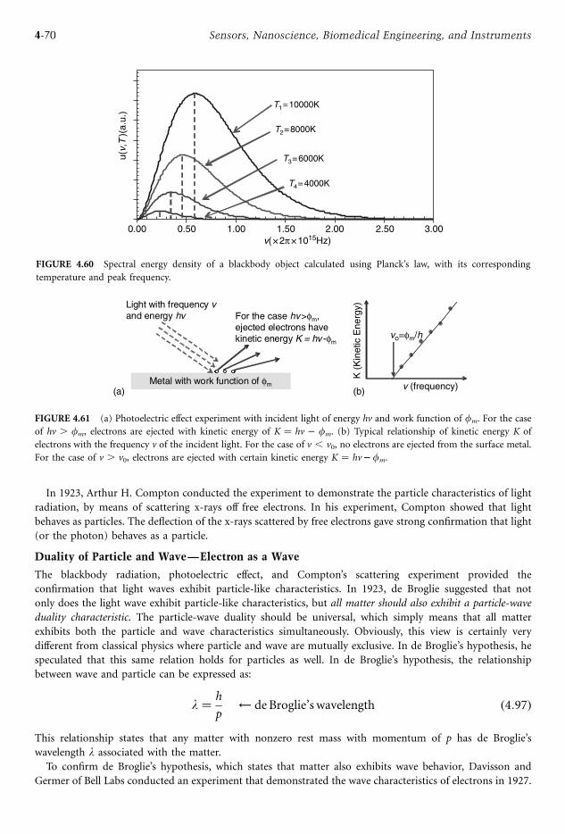
In 1923, Arthur H. Compton conducted the experiment to demonstrate the particle characteristics of light
radiation, by means of scattering x-rays off free electrons. In his experiment, Compton showed that light
behaves as particles. The deflection of the x-rays scattered by free electrons gave strong confirmation that light
(or the photon) behaves as a particle.
Duality of Particle and Wave—Electron as a Wave
The blackbody radiation, photoelectric effect, and Compton’s scattering experiment provided the
confirmation that light waves exhibit particle-like characteristics. In 1923, de Broglie suggested that not
only does the light wave exhibit particle-like characteristics, but all matter should also exhibit a particle-wave
duality characteristic. The particle-wave duality should be universal, which simply means that all matter
exhibits both the particle and wave characteristics simultaneously. Obviously, this view is certainly very
different from classical physics where particle and wave are mutually exclusive. In de Broglie’s hypothesis, he
speculated that this same relation holds for particles as well. In de Broglie’s hypothesis, the relationship
between wave and particle can be expressed as:
l ¼ h
pde Broglie’s wavelength ð4:97Þ
This relationship states that any matter with nonzero rest mass with momentum of p has de Broglie’s
wavelength l associated with the matter.To confirm de Broglie’s hypothesis, which states that matter also exhibits wave behavior, Davisson and
Germer of Bell Labs conducted an experiment that demonstrated the wave characteristics of electrons in 1927.
Light with frequency vand energy hv For the case hv>φm,
ejected electrons havekinetic energy K = hv -φm
Metal with work function of φm v (frequency)
K(K
inet
icE
nerg
y)
vo=φm/h
(a) (b)
FIGURE 4.61 (a) Photoelectric effect experiment with incident light of energy hv and work function of fm. For the caseof hv . fm, electrons are ejected with kinetic energy of K ¼ hv fm. (b) Typical relationship of kinetic energy K of
electrons with the frequency v of the incident light. For the case of v , v0, no electrons are ejected from the surface metal.
For the case of v . v0, electrons are ejected with certain kinetic energy K ¼ hv fm.
0.00 0.50 1.00 1.50 2.00 2.50 3.00v(×2π×1015Hz)
u(v,
T)(
a.u.
)
T1=10000K
T2=8000K
T3=6000K
T4=4000K
FIGURE 4.60 Spectral energy density of a blackbody object calculated using Planck’s law, with its corresponding
temperature and peak frequency.
4-70 Sensors, Nanoscience, Biomedical Engineering, and Instruments
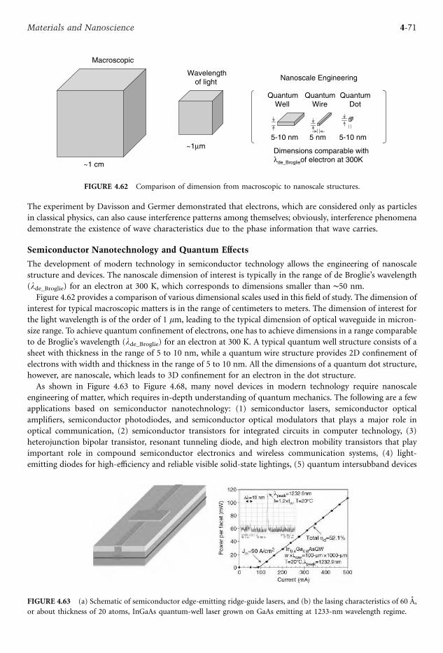
The experiment by Davisson and Germer demonstrated that electrons, which are considered only as particles
in classical physics, can also cause interference patterns among themselves; obviously, interference phenomena
demonstrate the existence of wave characteristics due to the phase information that wave carries.
Semiconductor Nanotechnology and Quantum Effects
The development of modern technology in semiconductor technology allows the engineering of nanoscale
structure and devices. The nanoscale dimension of interest is typically in the range of de Broglie’s wavelength
(lde_Broglie) for an electron at 300 K, which corresponds to dimensions smaller than 50 nm.
Figure 4.62 provides a comparison of various dimensional scales used in this field of study. The dimension of
interest for typical macroscopic matters is in the range of centimeters to meters. The dimension of interest for
the light wavelength is of the order of 1 mm, leading to the typical dimension of optical waveguide in micron-size range. To achieve quantum confinement of electrons, one has to achieve dimensions in a range comparable
to de Broglie’s wavelength (lde_Broglie) for an electron at 300 K. A typical quantum well structure consists of a
sheet with thickness in the range of 5 to 10 nm, while a quantum wire structure provides 2D confinement of
electrons with width and thickness in the range of 5 to 10 nm. All the dimensions of a quantum dot structure,
however, are nanoscale, which leads to 3D confinement for an electron in the dot structure.
As shown in Figure 4.63 to Figure 4.68, many novel devices in modern technology require nanoscale
engineering of matter, which requires in-depth understanding of quantum mechanics. The following are a few
applications based on semiconductor nanotechnology: (1) semiconductor lasers, semiconductor optical
amplifiers, semiconductor photodiodes, and semiconductor optical modulators that plays a major role in
optical communication, (2) semiconductor transistors for integrated circuits in computer technology, (3)
heterojunction bipolar transistor, resonant tunneling diode, and high electron mobility transistors that play
important role in compound semiconductor electronics and wireless communication systems, (4) light-
emitting diodes for high-efficiency and reliable visible solid-state lightings, (5) quantum intersubband devices
5-10 nm 5 nm 5-10 nm
QuantumWell
QuantumWire
QuantumDot
Macroscopic
Wavelengthof light
~1 cm
~1μm
Nanoscale Engineering
Dimensions comparable withλde_Broglieof electron at 300K
FIGURE 4.62 Comparison of dimension from macroscopic to nanoscale structures.
FIGURE 4.63 (a) Schematic of semiconductor edge-emitting ridge-guide lasers, and (b) the lasing characteristics of 60 A,
or about thickness of 20 atoms, InGaAs quantum-well laser grown on GaAs emitting at 1233-nm wavelength regime.
4-71Materials and Nanoscience
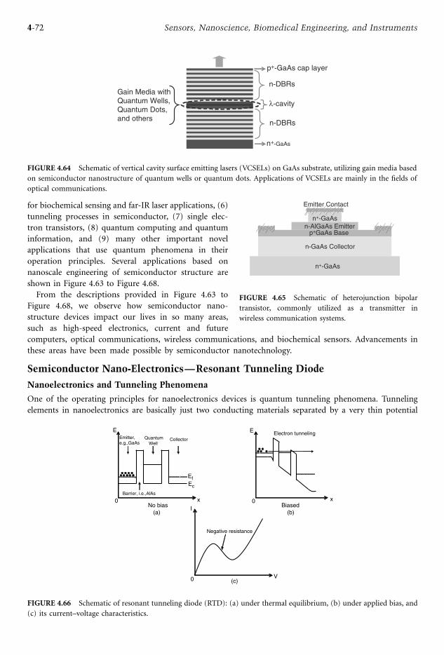
for biochemical sensing and far-IR laser applications, (6)
tunneling processes in semiconductor, (7) single elec-
tron transistors, (8) quantum computing and quantum
information, and (9) many other important novel
applications that use quantum phenomena in their
operation principles. Several applications based on
nanoscale engineering of semiconductor structure are
shown in Figure 4.63 to Figure 4.68.
From the descriptions provided in Figure 4.63 to
Figure 4.68, we observe how semiconductor nano-
structure devices impact our lives in so many areas,
such as high-speed electronics, current and future
computers, optical communications, wireless communications, and biochemical sensors. Advancements in
these areas have been made possible by semiconductor nanotechnology.
Semiconductor Nano-Electronics—Resonant Tunneling Diode
Nanoelectronics and Tunneling Phenomena
One of the operating principles for nanoelectronics devices is quantum tunneling phenomena. Tunneling
elements in nanoelectronics are basically just two conducting materials separated by a very thin potential
Gain Media withQuantum Wells,Quantum Dots,and others
λ-cavity
n-DBRs
n+-GaAs
n-DBRs
p+-GaAs cap layer
FIGURE 4.64 Schematic of vertical cavity surface emitting lasers (VCSELs) on GaAs substrate, utilizing gain media based
on semiconductor nanostructure of quantum wells or quantum dots. Applications of VCSELs are mainly in the fields of
optical communications.
n-GaAs Collector
p+GaAs Basen-AlGaAs Emitter
n+-GaAs
n+-GaAs
Emitter Contact
FIGURE 4.65 Schematic of heterojunction bipolar
transistor, commonly utilized as a transmitter in
wireless communication systems.
I
V
Negative resistance
E
x x
E Electron tunnelingEmitter,e.g.,GaAs
QuantumWell
Ef
Collector
Barrier, i.e.,AlAs
No bias Biased
Ec
0
0
0
(a) (b)
(c)
FIGURE 4.66 Schematic of resonant tunneling diode (RTD): (a) under thermal equilibrium, (b) under applied bias, and
(c) its current–voltage characteristics.
4-72 Sensors, Nanoscience, Biomedical Engineering, and Instruments
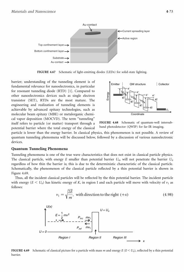
barrier; understanding of the tunneling element is of
fundamental relevance for nanoelectronics, in particular
for resonant tunneling diode (RTD) [1]. Compared to
other nanoelectronics devices such as single electron
transistor (SET), RTDs are the most mature. The
engineering and realization of tunneling elements is
achievable by advanced epitaxy technologies, such as
molecular beam epitaxy (MBE) or metalorganic chemi-
cal vapor deposition (MOCVD). The term ‘‘tunneling’’
itself refers to particle (or matter) transport through a
potential barrier where the total energy of the classical
particle is lower than the energy barrier. In classical physics, this phenomenon is not possible. A review of
quantum tunneling phenomena will be discussed below, followed by a discussion of various nanoelectronic
devices.
Quantum Tunneling Phenomena
Tunneling phenomena is one of the true wave characteristics that does not exist in classical particle physics.
The classical particle, with energy E smaller than potential barrier U0, will not penetrate the barrier U0
regardless of how thin the barrier is; this is due to the deterministic characteristic of the classical particle.
Schematically, the phenomenon of the classical particle reflected by a thin potential barrier is shown in
Figure 4.69.
Thus, all the incident classical particles will be reflected by the thin potential barrier. The incident particle
with energy (E , U0) has kinetic energy of K, in region I and each particle will move with velocity of v1 as
follows:
v1 ¼ffiffiffiffi2E
m
r; with direction to the right ðþxÞ ð4:98Þ
Region I Region II Region III
U(x)
U = 0
2
1mv 2E =
mv1
mv1
Pinc
Pref
U = Uo
x
FIGURE 4.69 Schematic of classical picture for a particle with mass m and energy E (E,U0), reflected by a thin potential
barrier.
Au-contact
Au-contact
Substrate
Bottom confinement layer
Top confinement layer
Active region
Current spreading layer
FIGURE 4.67 Schematic of light-emitting diodes (LEDs) for solid-state lighting.
e-
e-
e-
e-
e- e-
Emitter QW structure Collector
Ene
rgy
Coordinate
Ef
e-e−
e−
e− e−
e−e-
e-e−e−
e−e−
FIGURE 4.68 Schematic of quantum-well intersub-
band photodetector (QWIP) for far-IR imaging.
4-73Materials and Nanoscience
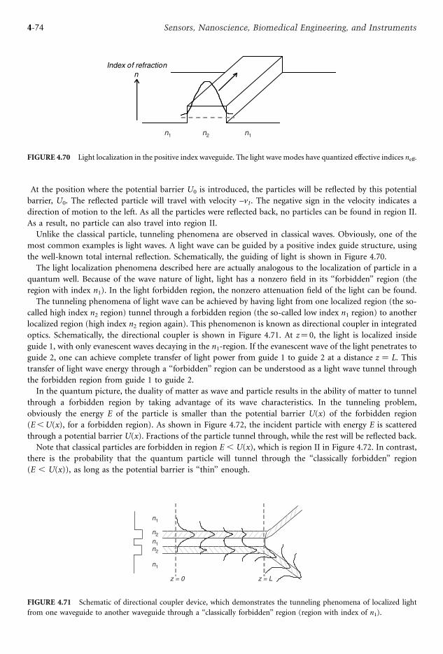
At the position where the potential barrier U0 is introduced, the particles will be reflected by this potential
barrier, U0. The reflected particle will travel with velocity –v1. The negative sign in the velocity indicates a
direction of motion to the left. As all the particles were reflected back, no particles can be found in region II.
As a result, no particle can also travel into region II.
Unlike the classical particle, tunneling phenomena are observed in classical waves. Obviously, one of the
most common examples is light waves. A light wave can be guided by a positive index guide structure, using
the well-known total internal reflection. Schematically, the guiding of light is shown in Figure 4.70.
The light localization phenomena described here are actually analogous to the localization of particle in a
quantum well. Because of the wave nature of light, light has a nonzero field in its ‘‘forbidden’’ region (the
region with index n1). In the light forbidden region, the nonzero attenuation field of the light can be found.
The tunneling phenomena of light wave can be achieved by having light from one localized region (the so-
called high index n2 region) tunnel through a forbidden region (the so-called low index n1 region) to another
localized region (high index n2 region again). This phenomenon is known as directional coupler in integrated
optics. Schematically, the directional coupler is shown in Figure 4.71. At z¼ 0, the light is localized inside
guide 1, with only evanescent waves decaying in the n1-region. If the evanescent wave of the light penetrates to
guide 2, one can achieve complete transfer of light power from guide 1 to guide 2 at a distance z ¼ L. This
transfer of light wave energy through a ‘‘forbidden’’ region can be understood as a light wave tunnel through
the forbidden region from guide 1 to guide 2.
In the quantum picture, the duality of matter as wave and particle results in the ability of matter to tunnel
through a forbidden region by taking advantage of its wave characteristics. In the tunneling problem,
obviously the energy E of the particle is smaller than the potential barrier U(x) of the forbidden region
(E,U(x), for a forbidden region). As shown in Figure 4.72, the incident particle with energy E is scattered
through a potential barrier U(x). Fractions of the particle tunnel through, while the rest will be reflected back.
Note that classical particles are forbidden in region E , U(x), which is region II in Figure 4.72. In contrast,
there is the probability that the quantum particle will tunnel through the ‘‘classically forbidden’’ region
(E , U(x)), as long as the potential barrier is ‘‘thin’’ enough.
n1 n2 n1
Index of refractionn
FIGURE 4.70 Light localization in the positive index waveguide. The light wave modes have quantized effective indices neff.
n1
n2
n1
n1
n2
z = 0 z = L
FIGURE 4.71 Schematic of directional coupler device, which demonstrates the tunneling phenomena of localized light
from one waveguide to another waveguide through a ‘‘classically forbidden’’ region (region with index of n1).
4-74 Sensors, Nanoscience, Biomedical Engineering, and Instruments
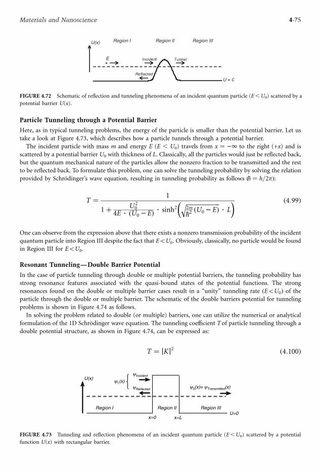
Particle Tunneling through a Potential Barrier
Here, as in typical tunneling problems, the energy of the particle is smaller than the potential barrier. Let us
take a look at Figure 4.73, which describes how a particle tunnels through a potential barrier.
The incident particle with mass m and energy E (E , U0) travels from x ¼ 1 to the right (+x) and is
scattered by a potential barrier U0 with thickness of L. Classically, all the particles would just be reflected back,
but the quantum mechanical nature of the particles allow the nonzero fraction to be transmitted and the rest
to be reflected back. To formulate this problem, one can solve the tunneling probability by solving the relation
provided by Schrodinger’s wave equation, resulting in tunneling probability as follows ðh ¼ h=2pÞ:
T ¼ 1
1þ U20
4E ðU0 EÞ sinh2ffiffiffiffiffiffiffiffiffiffiffiffiffiffi2m
h2ðU0 EÞ
qL
ð4:99Þ
One can observe from the expression above that there exists a nonzero transmission probability of the incident
quantum particle into Region III despite the fact that E5U0. Obviously, classically, no particle would be found
in Region III for E5U0.
Resonant Tunneling—Double Barrier Potential
In the case of particle tunneling through double or multiple potential barriers, the tunneling probability has
strong resonance features associated with the quasi-bound states of the potential functions. The strong
resonances found on the double or multiple barrier cases result in a ‘‘unity’’ tunneling rate ðE5U0Þ of theparticle through the double or multiple barrier. The schematic of the double barriers potential for tunneling
problems is shown in Figure 4.74 as follows.
In solving the problem related to double (or multiple) barriers, one can utilize the numerical or analytical
formulation of the 1D Schrodinger wave equation. The tunneling coefficient Tof particle tunneling through a
double potential structure, as shown in Figure 4.74, can be expressed as:
T ¼ jKj2 ð4:100Þ
yIncident
yReflected y3(x)= yTransmitted(x)
Region I Region II Region III
x=0 x=L
y1(x)U(x)
U=0
FIGURE 4.73 Tunneling and reflection phenomena of an incident quantum particle (E,U0) scattered by a potential
function U(x) with rectangular barrier.
Region I Region II Region IIIU(x)
U = 0
E Incident
Reflected
Tunnel
FIGURE 4.72 Schematic of reflection and tunneling phenomena of an incident quantum particle (E,U0) scattered by a
potential barrier U(x).
4-75Materials and Nanoscience

with 1/K reads:
1
K¼ ei2k
L2það Þ
4a2 k2ei2k L ða2þ k2Þ2 sinh2ða aÞ ða4þ k4Þ sinh2ða aÞþa2 k2 ½1þ 3coshð2a aÞ þ i2a k ða2 k2Þ sinhð2a aÞ
8<:9=; ð4:101Þ
k and a can be expressed as:
k¼ffiffiffiffiffiffi2mE
h2
sð4:102Þ
a¼ffiffiffiffiffiffiffiffiffiffiffiffiffiffi2m
h2ðU0 EÞ
sð4:103Þ
As an example, the transmission or tunneling coefficient T is plotted in Figure 4.75 for the case of U0 ¼ 1:2 eV,
L¼ 6 nm, and a¼ 1 nm. From the example presented here, we observe the existence of three resonance states
U(x)
Region I Region II Region III Region IV Region V
E
U=U0
U=00=x
2L
x =2L
x −= a2L
x +=+−= a2L
x
FIGURE 4.74 Schematic of double barrier potential function U(x) for tunneling problems of an incident quantum
particle with mass m and energy E.
m=0.067m0
U0=1.2(eV)L=6(nm)a=1(nm)
1.0E-06
1.0E-05
1.0E-04
1.0E-03
1.0E-02
1.0E-01
1.0E+00
0.0 0.2 0.4 0.6 0.8 1.0E/U0
log[
T(E
)]
ResonanceE1
ResonanceE2
ResonanceE3
FIGURE 4.75 Tunneling coefficient as function of energy E for a particle with mass m, scattered by a double barrier
potential. Notice the resonant features that occur at E1, E2, and E3, which also correspond to the quasi-bound states.
4-76 Sensors, Nanoscience, Biomedical Engineering, and Instruments
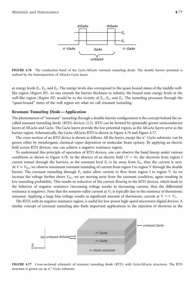
at energy levels E1, E2, and E3. The energy levels also correspond to the quasi-bound states of the middle-well-
like region (Region III). As one extends the barrier thickness to infinity, the bound state energy levels in the
well-like region (Region III) would be in the vicinity of E1, E2, and E3. The tunneling processes through the
‘‘quasi-bound’’ states of the well region are what we call resonant tunneling.
Resonant Tunneling Diode—Application
The phenomenon of ‘‘resonant’’ tunneling through a double-barrier configuration is the concept behind the so-
called resonant tunneling diode (RTD) devices [2,3]. RTD can be formed by epitaxially grown semiconductor
layers of AlGaAs and GaAs. The GaAs layers provide the low potential region, as the AlGaAs layers serve as the
barrier region. Schematically, the GaAs–AlGaAs RTD is shown in Figure 4.76 and Figure 4.77.
The cross-section of an RTD device is shown as follows. All the layers, except the n+-GaAs substrate, can be
grown either by metalorganic chemical vapor deposition or molecular beam epitaxy. By applying an electric
field across RTD devices, one can achieve a negative resistance region.
To understand this principle of operation of RTD devices, one can observe the band lineup under various
conditions as shown in Figure 4.78. In the absence of an electric field (V ¼ 0), the electrons from region I
cannot tunnel through the barriers, as the resonant level E1 is far away from Ef1, thus the current is zero.
At V ¼ VR1, we observe maximum resonant tunneling of current from region I to region V through the double
barrier. The resonant tunneling through E1 states allow current to flow from region I to region V. As we
increase the voltage further above VR1, we are moving away from the resonant condition, again resulting in
low tunneling probability. This results in reduction of the current flowing in the RTD devices, which leads to
the behavior of negative resistance (increasing voltage results in decreasing current, thus the differential
resistance is negative). Note that the nonzero valley current at V2 is typically due to the existence of thermionic
emission. Applying a large bias voltage results in significant amount of thermionic current at V .. V2.
The RTD, with its negative resistance region, is useful for low-power high-speed microwave digital devices. A
similar concept of resonant tunneling also finds important applications in the injection of electrons in the
E2
E1
AlGaAs AlGaAs
GaAs n+-GaAsn+-GaAs
undoped
FIGURE 4.76 The conduction band of the GaAs-AlGaAs resonant tunneling diode. The double barrier potential is
realized by the heterojunction of AlGaAs–GaAs layers.
n+-GaAsundoped AlGaAs
n+-GaAs substrate
n+-GaAs
undoped GaAs
U(x
)
FIGURE 4.77 Cross-sectional schematic of resonant tunneling diode (RTD) with GaAs/AlGaAs structures. The RTD
structure is grown on an nþ-GaAs substrate.
4-77Materials and Nanoscience
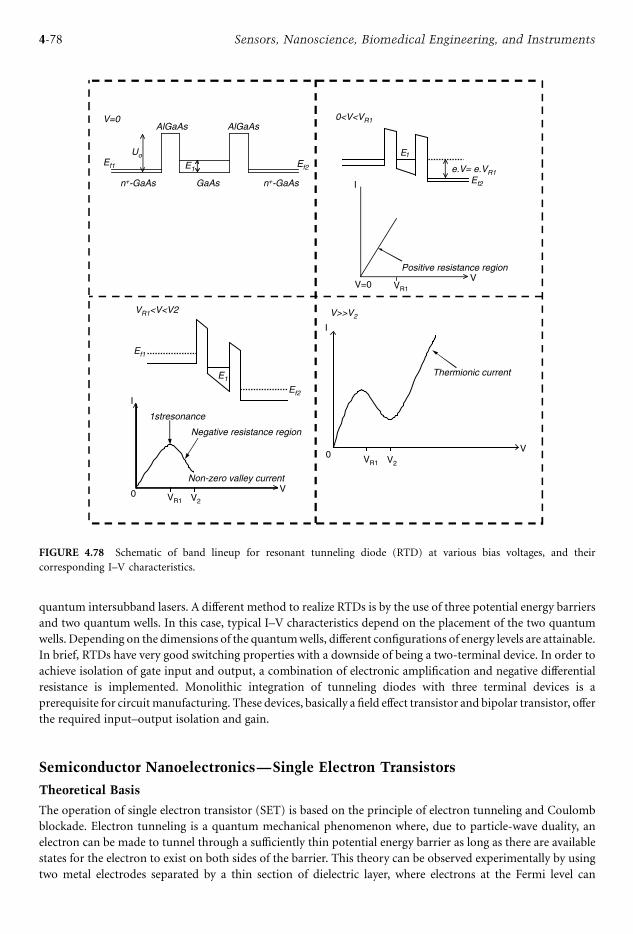
quantum intersubband lasers. A different method to realize RTDs is by the use of three potential energy barriers
and two quantum wells. In this case, typical I–V characteristics depend on the placement of the two quantum
wells. Depending on the dimensions of the quantumwells, different configurations of energy levels are attainable.
In brief, RTDs have very good switching properties with a downside of being a two-terminal device. In order to
achieve isolation of gate input and output, a combination of electronic amplification and negative differential
resistance is implemented. Monolithic integration of tunneling diodes with three terminal devices is a
prerequisite for circuitmanufacturing. These devices, basically a field effect transistor and bipolar transistor, offer
the required input–output isolation and gain.
Semiconductor Nanoelectronics—Single Electron Transistors
Theoretical Basis
The operation of single electron transistor (SET) is based on the principle of electron tunneling and Coulomb
blockade. Electron tunneling is a quantum mechanical phenomenon where, due to particle-wave duality, an
electron can be made to tunnel through a sufficiently thin potential energy barrier as long as there are available
states for the electron to exist on both sides of the barrier. This theory can be observed experimentally by using
two metal electrodes separated by a thin section of dielectric layer, where electrons at the Fermi level can
E1
AlGaAs AlGaAs
GaAsn+-GaAs n+-GaAs
UoEf1 Ef2
V=0
Ef2
E1
e.V= e.VR1
0<V<VR1
I
VPositive resistance region
V=0 VR1
I
V
Negative resistance region
0
1stresonance
Non-zero valley current
VR1 V2
VR1 V2
Ef1
Ef2
E1
VR1<V<V2
I
V0
Thermionic current
V>>V2
FIGURE 4.78 Schematic of band lineup for resonant tunneling diode (RTD) at various bias voltages, and their
corresponding I–V characteristics.
4-78 Sensors, Nanoscience, Biomedical Engineering, and Instruments
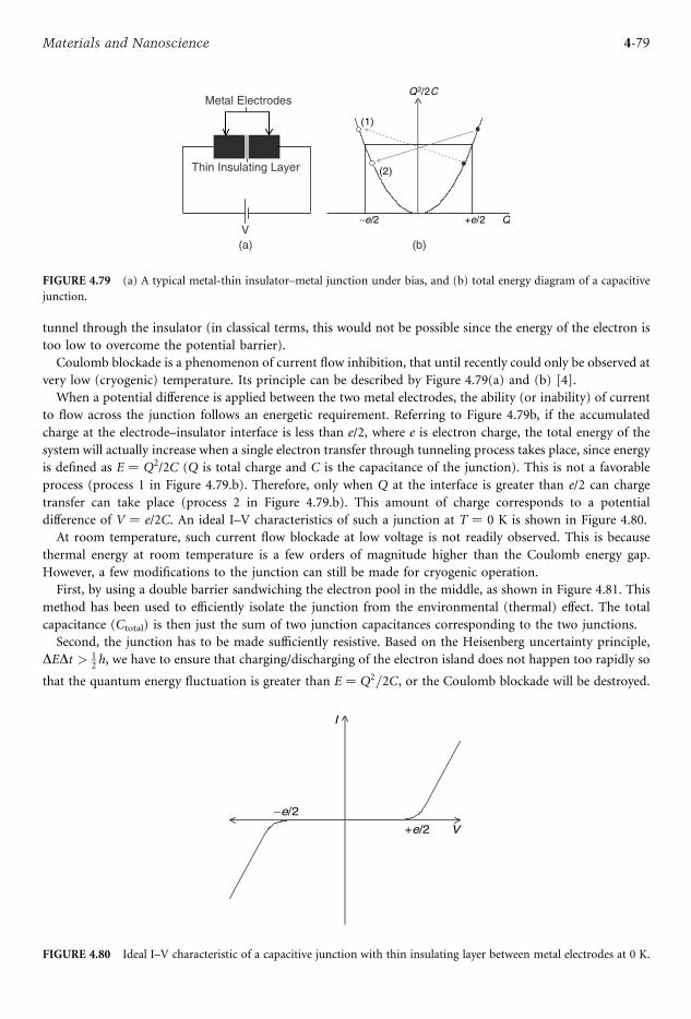
tunnel through the insulator (in classical terms, this would not be possible since the energy of the electron is
too low to overcome the potential barrier).
Coulomb blockade is a phenomenon of current flow inhibition, that until recently could only be observed at
very low (cryogenic) temperature. Its principle can be described by Figure 4.79(a) and (b) [4].
When a potential difference is applied between the two metal electrodes, the ability (or inability) of current
to flow across the junction follows an energetic requirement. Referring to Figure 4.79b, if the accumulated
charge at the electrode–insulator interface is less than e/2, where e is electron charge, the total energy of the
system will actually increase when a single electron transfer through tunneling process takes place, since energy
is defined as E ¼ Q2/2C (Q is total charge and C is the capacitance of the junction). This is not a favorable
process (process 1 in Figure 4.79.b). Therefore, only when Q at the interface is greater than e/2 can charge
transfer can take place (process 2 in Figure 4.79.b). This amount of charge corresponds to a potential
difference of V ¼ e/2C. An ideal I–V characteristics of such a junction at T ¼ 0 K is shown in Figure 4.80.
At room temperature, such current flow blockade at low voltage is not readily observed. This is because
thermal energy at room temperature is a few orders of magnitude higher than the Coulomb energy gap.
However, a few modifications to the junction can still be made for cryogenic operation.
First, by using a double barrier sandwiching the electron pool in the middle, as shown in Figure 4.81. This
method has been used to efficiently isolate the junction from the environmental (thermal) effect. The total
capacitance (Ctotal) is then just the sum of two junction capacitances corresponding to the two junctions.
Second, the junction has to be made sufficiently resistive. Based on the Heisenberg uncertainty principle,
DEDt > 12 h, we have to ensure that charging/discharging of the electron island does not happen too rapidly so
that the quantum energy fluctuation is greater than E ¼ Q2=2C, or the Coulomb blockade will be destroyed.
I
−e/2
+e/2 V
FIGURE 4.80 Ideal I–V characteristic of a capacitive junction with thin insulating layer between metal electrodes at 0 K.
Metal Electrodes
Thin Insulating Layer
V(a) (b)
Q2/2C
(1)
(2)
−e/2 +e/2 Q
FIGURE 4.79 (a) A typical metal-thin insulator–metal junction under bias, and (b) total energy diagram of a capacitive
junction.
4-79Materials and Nanoscience
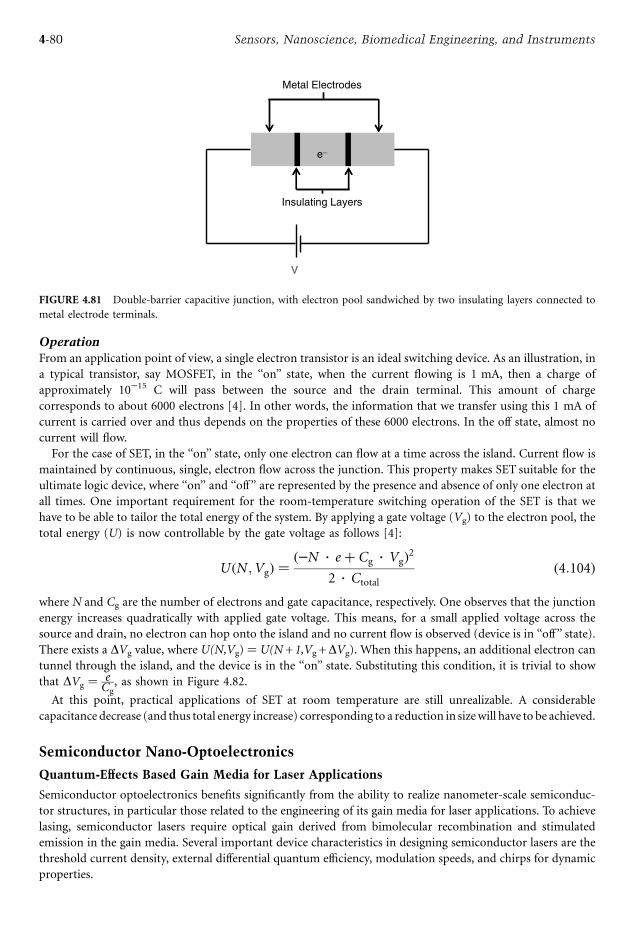
Operation
From an application point of view, a single electron transistor is an ideal switching device. As an illustration, in
a typical transistor, say MOSFET, in the ‘‘on’’ state, when the current flowing is 1 mA, then a charge of
approximately 10 15 C will pass between the source and the drain terminal. This amount of charge
corresponds to about 6000 electrons [4]. In other words, the information that we transfer using this 1 mA of
current is carried over and thus depends on the properties of these 6000 electrons. In the off state, almost no
current will flow.
For the case of SET, in the ‘‘on’’ state, only one electron can flow at a time across the island. Current flow is
maintained by continuous, single, electron flow across the junction. This property makes SET suitable for the
ultimate logic device, where ‘‘on’’ and ‘‘off ’’ are represented by the presence and absence of only one electron at
all times. One important requirement for the room-temperature switching operation of the SET is that we
have to be able to tailor the total energy of the system. By applying a gate voltage (Vg) to the electron pool, the
total energy (U) is now controllable by the gate voltage as follows [4]:
UðN;VgÞ ¼ð N eþ Cg VgÞ2
2 Ctotalð4:104Þ
where N and Cg are the number of electrons and gate capacitance, respectively. One observes that the junction
energy increases quadratically with applied gate voltage. This means, for a small applied voltage across the
source and drain, no electron can hop onto the island and no current flow is observed (device is in ‘‘off ’’ state).
There exists a DVg value, where U(N,Vg) ¼ U(N+ 1,Vg +DVg). When this happens, an additional electron can
tunnel through the island, and the device is in the ‘‘on’’ state. Substituting this condition, it is trivial to show
that DVg ¼ eCg, as shown in Figure 4.82.
At this point, practical applications of SET at room temperature are still unrealizable. A considerable
capacitance decrease (and thus total energy increase) corresponding to a reduction in sizewill have to be achieved.
Semiconductor Nano-Optoelectronics
Quantum-Effects Based Gain Media for Laser Applications
Semiconductor optoelectronics benefits significantly from the ability to realize nanometer-scale semiconduc-
tor structures, in particular those related to the engineering of its gain media for laser applications. To achieve
lasing, semiconductor lasers require optical gain derived from bimolecular recombination and stimulated
emission in the gain media. Several important device characteristics in designing semiconductor lasers are the
threshold current density, external differential quantum efficiency, modulation speeds, and chirps for dynamic
properties.
Metal Electrodes
Insulating Layers
V
e−
FIGURE 4.81 Double-barrier capacitive junction, with electron pool sandwiched by two insulating layers connected to
metal electrode terminals.
4-80 Sensors, Nanoscience, Biomedical Engineering, and Instruments
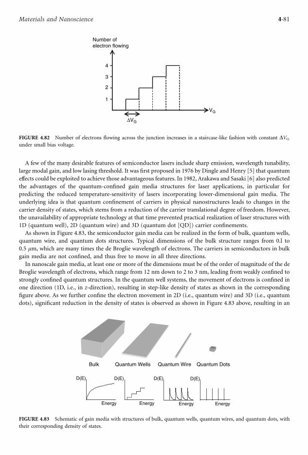
A few of the many desirable features of semiconductor lasers include sharp emission, wavelength tunability,
large modal gain, and low lasing threshold. It was first proposed in 1976 by Dingle and Henry [5] that quantum
effects could be exploited to achieve those advantageous features. In 1982, Arakawa and Sasaki [6] also predicted
the advantages of the quantum-confined gain media structures for laser applications, in particular for
predicting the reduced temperature-sensitivity of lasers incorporating lower-dimensional gain media. The
underlying idea is that quantum confinement of carriers in physical nanostructures leads to changes in the
carrier density of states, which stems from a reduction of the carrier translational degree of freedom. However,
the unavailability of appropriate technology at that time prevented practical realization of laser structures with
1D (quantum well), 2D (quantum wire) and 3D (quantum dot [QD]) carrier confinements.
As shown in Figure 4.83, the semiconductor gain media can be realized in the form of bulk, quantum wells,
quantum wire, and quantum dots structures. Typical dimensions of the bulk structure ranges from 0.l to
0.5 mm, which are many times the de Broglie wavelength of electrons. The carriers in semiconductors in bulkgain media are not confined, and thus free to move in all three directions.
In nanoscale gain media, at least one or more of the dimensions must be of the order of magnitude of the de
Broglie wavelength of electrons, which range from 12 nm down to 2 to 3 nm, leading from weakly confined to
strongly confined quantum structures. In the quantum well systems, the movement of electrons is confined in
one direction (1D, i.e., in z-direction), resulting in step-like density of states as shown in the corresponding
figure above. As we further confine the electron movement in 2D (i.e., quantum wire) and 3D (i.e., quantum
dots), significant reduction in the density of states is observed as shown in Figure 4.83 above, resulting in an
Bulk Quantum DotsQuantum Wells Quantum Wire
D(E)
Energy
D(E) D(E) D(E)
EnergyEnergy Energy
FIGURE 4.83 Schematic of gain media with structures of bulk, quantum wells, quantum wires, and quantum dots, with
their corresponding density of states.
Number ofelectron flowing
VG
1
2
3
4
∆VG
FIGURE 4.82 Number of electrons flowing across the junction increases in a staircase-like fashion with constant DVGunder small bias voltage.
4-81Materials and Nanoscience
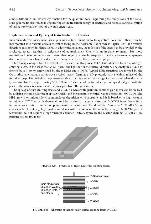
almost delta-function-like density function for the quantum dots. Engineering the dimensions of the nano-
scale gain media also results in engineering of the transition energy of electrons and holes, allowing alteration
of lasing wavelength on top of the bulk energy gap.
Implementation and Epitaxy of Gain Media into Devices
In semiconductor lasers, nano scale gain media (i.e., quantum wells, quantum dots, and others) can be
incorporated into various devices to realize lasing in the horizontal (as shown in Figure 4.84) and vertical
directions (as shown in Figure 4.85). In edge emitting lasers, the reflector of the lasers can be provided by the
as-cleaved facets resulting in reflectance of approximately 30% with an in-plane resonator. For more
sophisticated telecommunication lasers that require a single frequency, device structures employing
distributed feedback lasers or distributed Bragg reflectors (DBRs) can be employed.
The principle of operation for vertical cavity surface emitting lasers (VCSELs) is different from that of edge-
emitting lasers, in the sense that VCSELs emit the light out in the vertical direction. The cavity in VCSELs is
formed by a l-cavity sandwiched by the p-DBRs and n-DBRs. Typical DBR structures are formed by the
GaAs–AlAs alternating quarter-wave stacked layers, forming a 1D photonic lattice with a range of the
forbidden gap. The forbidden gap corresponds to the high reflectivity range for certain wavelengths, with
typical stop band of approximately 50 to 100 nm. The center of the forbidden gap is typically aligned with the
peak of the cavity resonance and the peak gain from the gain media.
The epitaxy of edge-emitting lasers and VCSELs devices with quantum-confined gain media can be realized
by utilizing the molecular beam epitaxy (MBE) and metalorganic chemical vapor deposition (MOCVD). The
MBE growth technique allows submonolayer deposition on a substrate, and it is based on a high-vacuum
technique (10 11 Torr) with elemental crucibles serving as the growth sources. MOCVD is another epitaxy
technique widely utilized in the compound semiconductor research and industry. Similar to MBE, MOCVD is
also capable of realizing high-quality interfaces with precision in the monolayer range. MOCVD growth
techniques do not require a high vacuum chamber; instead, typically, the reactor chamber is kept at low
pressure (50 to 100 mbar).
FIGURE 4.84 Schematic of ridge-guide edge emitting lasers.
Gain Media withQuantum Wells,Quantum Dots,and others
λ-cavity
n-DBRs
n+-GaAs
n-DBRs
p+-GaAscap layer
FIGURE 4.85 Schematic of vertical cavity surface emitting lasers (VCSELs).
4-82 Sensors, Nanoscience, Biomedical Engineering, and Instruments
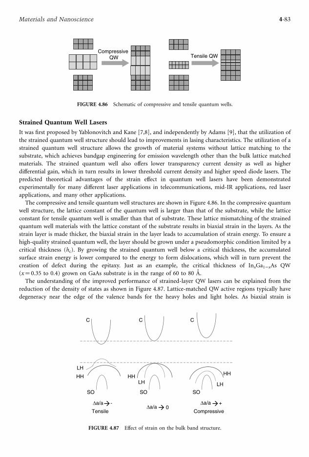
Strained Quantum Well Lasers
It was first proposed by Yablonovitch and Kane [7,8], and independently by Adams [9], that the utilization of
the strained quantum well structure should lead to improvements in lasing characteristics. The utilization of a
strained quantum well structure allows the growth of material systems without lattice matching to the
substrate, which achieves bandgap engineering for emission wavelength other than the bulk lattice matched
materials. The strained quantum well also offers lower transparency current density as well as higher
differential gain, which in turn results in lower threshold current density and higher speed diode lasers. The
predicted theoretical advantages of the strain effect in quantum well lasers have been demonstrated
experimentally for many different laser applications in telecommunications, mid-IR applications, red laser
applications, and many other applications.
The compressive and tensile quantum well structures are shown in Figure 4.86. In the compressive quantum
well structure, the lattice constant of the quantum well is larger than that of the substrate, while the lattice
constant for tensile quantum well is smaller than that of substrate. These lattice mismatching of the strained
quantum well materials with the lattice constant of the substrate results in biaxial strain in the layers. As the
strain layer is made thicker, the biaxial strain in the layer leads to accumulation of strain energy. To ensure a
high-quality strained quantum well, the layer should be grown under a pseudomorphic condition limited by a
critical thickness (hc). By growing the strained quantum well below a critical thickness, the accumulated
surface strain energy is lower compared to the energy to form dislocations, which will in turn prevent the
creation of defect during the epitaxy. Just as an example, the critical thickness of InxGa1 xAs QW
(x¼ 0.35 to 0.4) grown on GaAs substrate is in the range of 60 to 80 A.
The understanding of the improved performance of strained-layer QW lasers can be explained from the
reduction of the density of states as shown in Figure 4.87. Lattice-matched QW active regions typically have
degeneracy near the edge of the valence bands for the heavy holes and light holes. As biaxial strain is
CompressiveQW Tensile QW
FIGURE 4.86 Schematic of compressive and tensile quantum wells.
∆a/a 0∆a/a +
Compressive
∆a/a -
Tensile
C C C
LH
HH
SO
LHHH
SO
LH
HH
SO
FIGURE 4.87 Effect of strain on the bulk band structure.
4-83Materials and Nanoscience
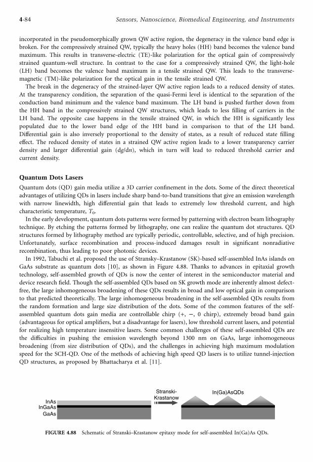
incorporated in the pseudomorphically grown QW active region, the degeneracy in the valence band edge is
broken. For the compressively strained QW, typically the heavy holes (HH) band becomes the valence band
maximum. This results in transverse-electric (TE)-like polarization for the optical gain of compressively
strained quantum-well structure. In contrast to the case for a compressively strained QW, the light-hole
(LH) band becomes the valence band maximum in a tensile strained QW. This leads to the transverse-
magnetic (TM)-like polarization for the optical gain in the tensile strained QW.
The break in the degeneracy of the strained-layer QW active region leads to a reduced density of states.
At the transparency condition, the separation of the quasi-Fermi level is identical to the separation of the
conduction band minimum and the valence band maximum. The LH band is pushed further down from
the HH band in the compressively strained QW structures, which leads to less filling of carriers in the
LH band. The opposite case happens in the tensile strained QW, in which the HH is significantly less
populated due to the lower band edge of the HH band in comparison to that of the LH band.
Differential gain is also inversely proportional to the density of states, as a result of reduced state filling
effect. The reduced density of states in a strained QW active region leads to a lower transparency carrier
density and larger differential gain (dg/dn), which in turn will lead to reduced threshold carrier and
current density.
Quantum Dots Lasers
Quantum dots (QD) gain media utilize a 3D carrier confinement in the dots. Some of the direct theoretical
advantages of utilizing QDs in lasers include sharp band-to-band transitions that give an emission wavelength
with narrow linewidth, high differential gain that leads to extremely low threshold current, and high
characteristic temperature, T0.
In the early development, quantum dots patterns were formed by patterning with electron beam lithography
technique. By etching the patterns formed by lithography, one can realize the quantum dot structures. QD
structures formed by lithography method are typically periodic, controllable, selective, and of high precision.
Unfortunately, surface recombination and process-induced damages result in significant nonradiative
recombination, thus leading to poor photonic devices.
In 1992, Tabuchi et al. proposed the use of Stransky–Krastanow (SK)-based self-assembled InAs islands on
GaAs substrate as quantum dots [10], as shown in Figure 4.88. Thanks to advances in epitaxial growth
technology, self-assembled growth of QDs is now the center of interest in the semiconductor material and
device research field. Though the self-assembled QDs based on SK growth mode are inherently almost defect-
free, the large inhomogeneous broadening of these QDs results in broad and low optical gain in comparison
to that predicted theoretically. The large inhomogeneous broadening in the self-assembled QDs results from
the random formation and large size distribution of the dots. Some of the common features of the self-
assembled quantum dots gain media are controllable chirp (+, , 0 chirp), extremely broad band gain
(advantageous for optical amplifiers, but a disadvantage for lasers), low threshold current lasers, and potential
for realizing high temperature insensitive lasers. Some common challenges of these self-assembled QDs are
the difficulties in pushing the emission wavelength beyond 1300 nm on GaAs, large inhomogeneous
broadening (from size distribution of QDs), and the challenges in achieving high maximum modulation
speed for the SCH-QD. One of the methods of achieving high speed QD lasers is to utilize tunnel-injection
QD structures, as proposed by Bhattacharya et al. [11].
GaAsInGaAs
InAs
Stranski-Krastanow
In(Ga)AsQDs
FIGURE 4.88 Schematic of Stranski–Krastanow epitaxy mode for self-assembled In(Ga)As QDs.
4-84 Sensors, Nanoscience, Biomedical Engineering, and Instruments
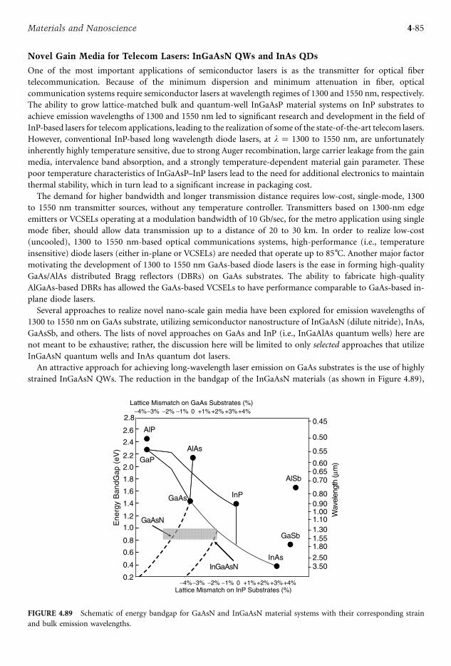
Novel Gain Media for Telecom Lasers: InGaAsN QWs and InAs QDs
One of the most important applications of semiconductor lasers is as the transmitter for optical fiber
telecommunication. Because of the minimum dispersion and minimum attenuation in fiber, optical
communication systems require semiconductor lasers at wavelength regimes of 1300 and 1550 nm, respectively.
The ability to grow lattice-matched bulk and quantum-well InGaAsP material systems on InP substrates to
achieve emission wavelengths of 1300 and 1550 nm led to significant research and development in the field of
InP-based lasers for telecom applications, leading to the realization of some of the state-of-the-art telecom lasers.
However, conventional InP-based long wavelength diode lasers, at l ¼ 1300 to 1550 nm, are unfortunately
inherently highly temperature sensitive, due to strong Auger recombination, large carrier leakage from the gain
media, intervalence band absorption, and a strongly temperature-dependent material gain parameter. These
poor temperature characteristics of InGaAsP–InP lasers lead to the need for additional electronics to maintain
thermal stability, which in turn lead to a significant increase in packaging cost.
The demand for higher bandwidth and longer transmission distance requires low-cost, single-mode, 1300
to 1550 nm transmitter sources, without any temperature controller. Transmitters based on 1300-nm edge
emitters or VCSELs operating at a modulation bandwidth of 10 Gb/sec, for the metro application using single
mode fiber, should allow data transmission up to a distance of 20 to 30 km. In order to realize low-cost
(uncooled), 1300 to 1550 nm-based optical communications systems, high-performance (i.e., temperature
insensitive) diode lasers (either in-plane or VCSELs) are needed that operate up to 85 C. Another major factor
motivating the development of 1300 to 1550 nm GaAs-based diode lasers is the ease in forming high-quality
GaAs/AlAs distributed Bragg reflectors (DBRs) on GaAs substrates. The ability to fabricate high-quality
AlGaAs-based DBRs has allowed the GaAs-based VCSELs to have performance comparable to GaAs-based in-
plane diode lasers.
Several approaches to realize novel nano-scale gain media have been explored for emission wavelengths of
1300 to 1550 nm on GaAs substrate, utilizing semiconductor nanostructure of InGaAsN (dilute nitride), InAs,
GaAsSb, and others. The lists of novel approaches on GaAs and InP (i.e., InGaAlAs quantum wells) here are
not meant to be exhaustive; rather, the discussion here will be limited to only selected approaches that utilize
InGaAsN quantum wells and InAs quantum dot lasers.
An attractive approach for achieving long-wavelength laser emission on GaAs substrates is the use of highly
strained InGaAsN QWs. The reduction in the bandgap of the InGaAsN materials (as shown in Figure 4.89),
FIGURE 4.89 Schematic of energy bandgap for GaAsN and InGaAsN material systems with their corresponding strain
and bulk emission wavelengths.
4-85Materials and Nanoscience
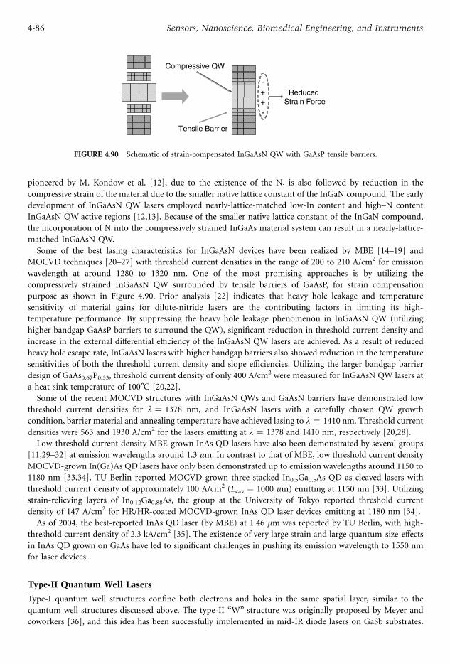
pioneered by M. Kondow et al. [12], due to the existence of the N, is also followed by reduction in the
compressive strain of the material due to the smaller native lattice constant of the InGaN compound. The early
development of InGaAsN QW lasers employed nearly-lattice-matched low-In content and high–N content
InGaAsN QW active regions [12,13]. Because of the smaller native lattice constant of the InGaN compound,
the incorporation of N into the compressively strained InGaAs material system can result in a nearly-lattice-
matched InGaAsN QW.
Some of the best lasing characteristics for InGaAsN devices have been realized by MBE [14–19] and
MOCVD techniques [20–27] with threshold current densities in the range of 200 to 210 A/cm2 for emission
wavelength at around 1280 to 1320 nm. One of the most promising approaches is by utilizing the
compressively strained InGaAsN QW surrounded by tensile barriers of GaAsP, for strain compensation
purpose as shown in Figure 4.90. Prior analysis [22] indicates that heavy hole leakage and temperature
sensitivity of material gains for dilute-nitride lasers are the contributing factors in limiting its high-
temperature performance. By suppressing the heavy hole leakage phenomenon in InGaAsN QW (utilizing
higher bandgap GaAsP barriers to surround the QW), significant reduction in threshold current density and
increase in the external differential efficiency of the InGaAsN QW lasers are achieved. As a result of reduced
heavy hole escape rate, InGaAsN lasers with higher bandgap barriers also showed reduction in the temperature
sensitivities of both the threshold current density and slope efficiencies. Utilizing the larger bandgap barrier
design of GaAs0.67P0.33, threshold current density of only 400 A/cm2 were measured for InGaAsN QW lasers at
a heat sink temperature of 100 C [20,22].
Some of the recent MOCVD structures with InGaAsN QWs and GaAsN barriers have demonstrated low
threshold current densities for l ¼ 1378 nm, and InGaAsN lasers with a carefully chosen QW growth
condition, barrier material and annealing temperature have achieved lasing to l ¼ 1410 nm. Threshold current
densities were 563 and 1930 A/cm2 for the lasers emitting at l ¼ 1378 and 1410 nm, respectively [20,28].
Low-threshold current density MBE-grown InAs QD lasers have also been demonstrated by several groups
[11,29–32] at emission wavelengths around 1.3 mm. In contrast to that of MBE, low threshold current density
MOCVD-grown In(Ga)As QD lasers have only been demonstrated up to emission wavelengths around 1150 to
1180 nm [33,34]. TU Berlin reported MOCVD-grown three-stacked In0.5Ga0.5As QD as-cleaved lasers with
threshold current density of approximately 100 A/cm2 (Lcav ¼ 1000 mm) emitting at 1150 nm [33]. Utilizing
strain-relieving layers of In0.12Ga0.88As, the group at the University of Tokyo reported threshold current
density of 147 A/cm2 for HR/HR-coated MOCVD-grown InAs QD laser devices emitting at 1180 nm [34].
As of 2004, the best-reported InAs QD laser (by MBE) at 1.46 mm was reported by TU Berlin, with high-
threshold current density of 2.3 kA/cm2 [35]. The existence of very large strain and large quantum-size-effects
in InAs QD grown on GaAs have led to significant challenges in pushing its emission wavelength to 1550 nm
for laser devices.
Type-II Quantum Well Lasers
Type-I quantum well structures confine both electrons and holes in the same spatial layer, similar to the
quantum well structures discussed above. The type-II ‘‘W’’ structure was originally proposed by Meyer and
coworkers [36], and this idea has been successfully implemented in mid-IR diode lasers on GaSb substrates.
++-
-Reduced
Strain Force
Compressive QW
Tensile Barrier
FIGURE 4.90 Schematic of strain-compensated InGaAsN QW with GaAsP tensile barriers.
4-86 Sensors, Nanoscience, Biomedical Engineering, and Instruments
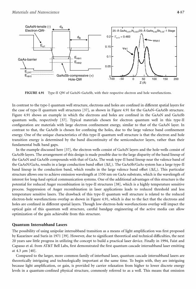
In contrast to the type-I quantum well structure, electrons and holes are confined in different spatial layers for
the case of type-II quantum well structures [37], as shown in Figure 4.91 for the GaAsN–GaAsSb structure.
Figure 4.91 shows an example in which the electrons and holes are confined in the GaAsN and GaAsSb
quantum wells, respectively [37]. Typical materials chosen for electron quantum well in this type-II
configuration are materials with large electron confinement energy, similar to that of the GaAsN layer. In
contrast to that, the GaAsSb is chosen for confining the holes, due to the large valence band confinement
energy. One of the unique characteristics of this type-II quantum well structure is that the electron and hole
transition energy is determined by the band discontinuity of the semiconductor layers, rather than their
fundamental bulk band gaps.
In the example discussed here [37], the electron wells consist of GaAsN layers and the hole-wells consist of
GaAsSb layers. The arrangement of this design is made possible due to the large disparity of the band lineup of
the GaAsN and GaAsSb compounds with that of GaAs. The weak type-II band lineup near the valence band of
the GaAsN/GaAs, results in a large conduction band offset (DEc). The GaAsSb/GaAs system has a large type-II
band lineup in the conduction band, which results in the large valence band offset (DEv). This particularstructure allows one to achieve emission wavelength at 1550 nm on GaAs substrate, which is the wavelength of
interest for long-haul optical communication systems. One of the additional advantages of this structure is the
potential for reduced Auger recombination in type-II structures [38], which is a highly temperature sensitive
process. Suppression of Auger recombination in laser applications leads to reduced threshold and less
temperature sensitive lasers. The drawback of this type-II quantum well structure is related to the reduced
electron-hole wavefunctions overlap as shown in Figure 4.91, which is due to the fact that the electrons and
holes are confined in different spatial layers. Though low electron-hole wavefunctions overlap will impact the
optical gain of this quantum well structure, careful bandgap engineering of the active media can allow
optimization of the gain achievable from this structure.
Quantum Intersubband Lasers
The possibility of using unipolar intersubband transition as a means of light amplification was first proposed
by Kazarinov and Suris in 1971 [39]. However, due to significant theoretical and technical difficulties, the next
20 years saw little progress in utilizing the concept to build a practical laser device. Finally in 1994, Faist and
Capasso et al. from AT&T Bell Labs, first demonstrated the first quantum cascade intersubband laser emitting
at 4.3 mm [40].
Compared to the larger, more common family of interband laser, quantum cascade intersubband lasers are
theoretically intriguing and technologically important at the same time. To begin with, they are intriguing
because light amplification, or gain, is provided by carrier relaxation from higher to lower discrete energy
levels in a quantum-confined physical structure, commonly referred to as a well. This means that emission
GaAsN-tensile (-)Electron-QW-
GaAsSb-compressive (+)Hole-QW
GaAs-barrier
Ee1
EHH2
EHH1
ELH1EHH1
dA
dB
25−Å GaAs0.977N0.023/25−Å GaAs0.65Sb0.35−1 Stage
0.2 Γe−h = 0.483
Ψe1
Ψhh1
0.15
0.1
0.05
0−100 −50 0 50
Z (Å)100 150 200
FIGURE 4.91 Type-II QW of GaAsN–GaAsSb, with their respective electron and hole wavefunctions.
4-87Materials and Nanoscience
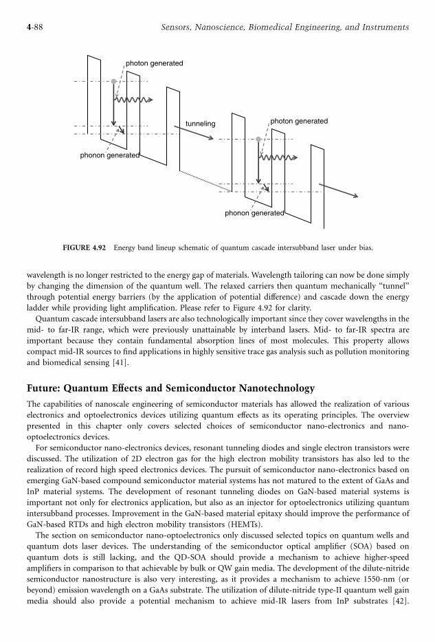
wavelength is no longer restricted to the energy gap of materials. Wavelength tailoring can now be done simply
by changing the dimension of the quantum well. The relaxed carriers then quantum mechanically ‘‘tunnel’’
through potential energy barriers (by the application of potential difference) and cascade down the energy
ladder while providing light amplification. Please refer to Figure 4.92 for clarity.
Quantum cascade intersubband lasers are also technologically important since they cover wavelengths in the
mid- to far-IR range, which were previously unattainable by interband lasers. Mid- to far-IR spectra are
important because they contain fundamental absorption lines of most molecules. This property allows
compact mid-IR sources to find applications in highly sensitive trace gas analysis such as pollution monitoring
and biomedical sensing [41].
Future: Quantum Effects and Semiconductor Nanotechnology
The capabilities of nanoscale engineering of semiconductor materials has allowed the realization of various
electronics and optoelectronics devices utilizing quantum effects as its operating principles. The overview
presented in this chapter only covers selected choices of semiconductor nano-electronics and nano-
optoelectronics devices.
For semiconductor nano-electronics devices, resonant tunneling diodes and single electron transistors were
discussed. The utilization of 2D electron gas for the high electron mobility transistors has also led to the
realization of record high speed electronics devices. The pursuit of semiconductor nano-electronics based on
emerging GaN-based compound semiconductor material systems has not matured to the extent of GaAs and
InP material systems. The development of resonant tunneling diodes on GaN-based material systems is
important not only for electronics application, but also as an injector for optoelectronics utilizing quantum
intersubband processes. Improvement in the GaN-based material epitaxy should improve the performance of
GaN-based RTDs and high electron mobility transistors (HEMTs).
The section on semiconductor nano-optoelectronics only discussed selected topics on quantum wells and
quantum dots laser devices. The understanding of the semiconductor optical amplifier (SOA) based on
quantum dots is still lacking, and the QD-SOA should provide a mechanism to achieve higher-speed
amplifiers in comparison to that achievable by bulk or QW gain media. The development of the dilute-nitride
semiconductor nanostructure is also very interesting, as it provides a mechanism to achieve 1550-nm (or
beyond) emission wavelength on a GaAs substrate. The utilization of dilute-nitride type-II quantum well gain
media should also provide a potential mechanism to achieve mid-IR lasers from InP substrates [42].
photon generated
phonon generated
tunneling photon generated
phonon generated
FIGURE 4.92 Energy band lineup schematic of quantum cascade intersubband laser under bias.
4-88 Sensors, Nanoscience, Biomedical Engineering, and Instruments

The development of the quantum intersubband devices based on GaN material systems is still lagging behind
that of the GaAs/InP material systems, mainly due to the difficulty in reducing the defect density in the GaN
material systems. As the material quality of GaN-based epitaxy is improved, the device physics and
performance of the GaN-based intersubband devices should be feasible for laser and switching applications.
Though self-assembled InAs QD lasers have demonstrated excellent lasing characteristics, the development of
InN QD lasers is still immature and requires further investigation.
References
1. K. Goser, P. Glosekotter, and J. Dienstuhl, Nanoelectronics and Nanosystems: from Transistors to
Molecular and Quantum Devices, Germany: Springer, 2004.
2. L. Esaki, Phys. Rev., 109, 603, 1958.
3. L. Esaki, IEEE Trans. Electron. Dev., ED-23, 644, 1976.
4. Keith Barnham and Dimitri Vvedenski, Eds., Low-Dimensional Semiconductor Structures: Fundamentals
and Device Applications, United Kingdom: Cambridge University Press, 2001.
5. R. Dingle, W. Wiegmann, and C.H. Henry, Phys. Rev. Lett., vol. 33, p. 827, 1974.
6. Y. Arakawa and H. Sasaki, Appl. Phys. Lett., 40, 939, 1982.
7. E. Yablonovitch and E.O. Kane, IEEE J. Lightwave Technol., LT-4, 504, 1986.
8. E. Yablonovitch and E.O. Kane, IEEE J. Lightwave Technol., LT-4, 961, 1986.
9. A.R. Adams, Electron. Lett., 22, 249, 1986.
10. M. Tabuchi et al., Science and Technology of Mesoscopic Structures, 1992, pp. 379–384.
11. S. Ghosh, S. Pradhan, and P. Bhattacharya, Appl. Phys. Lett., 81, 3055, 2002.
12. M. Kondow, T. Kitatani, S. Nakatsuka, M.C. Larson, K. Nakahara, Y. Yazawa, M. Okai, and K. Uomi,
IEEE J. Select. Topic Quant. Electron., 3, 719–730, 1997.
13. J.S. Harris, Jr., IEEE J. Select. Topics Quant. Electron., vol. 6, no. 6, pp. 1145–1160, 2000.
14. D.A. Livshits, A.Yu. Egorov, and H. Riechert, Electron. Lett., vol. 36, no. 16, pp. 1381–1382, 2000.
15. J. Wei, F. Xia, C. Li, and S.R. Forrest, IEEE Photon. Technol. Lett., 14, 597, 2002.
16. K.D. Choquette, J.F. Klem, A.J. Fischer, O. Blum, A.A. Allerman, I.J. Fritz, S.R. Kurtz, W.G. Breiland,
R. Sieg, K.M. Geib, J.W. Scott, and R.L. Naone, Electron. Lett., vol. 36, no. 16, pp. 1388–1390, 2000.
17. W. Ha, V. Gambin, M. Wistey, S. Bank, S. Kim, J.S. Harris, Jr., IEEE Photon. Technol. Lett., vol. 14 no. 5,
2002.
18. C.S. Peng, T. Jouhti, P. Laukkanen, E.-M. Pavelescu, J. Konttinen, W. Li, and M. Pessa, IEEE Photon.
Technol. Lett., vol. 14, no. 3, pp. 275–277, 2002.
19. W. Li, T. Jouhti, C.S. Peng, J. Konttinen, P. Laukkanen, E.-M. Pavelescu, and M. Pessa, Appl. Phys. Lett.,
vol. 79, no. 21, pp. 3386–3388, 2001.
20. N. Tansu, J.Y. Yeh, and L.J. Mawst, IOP J. Phys.: Condens. Matter Phys., 16, 2004 (August).
21. N. Tansu, N.J. Kirsch, and L.J. Mawst, Appl. Phys. Lett., vol. 81, no. 14, pp. 2523–2525, 2002.
22. N. Tansu, J.Y. Yeh, and L.J. Mawst, Appl. Phys. Lett., vol. 83, no.11, pp. 2112–2114, 2003.
23. N. Tansu, J.Y. Yeh, and L.J. Mawst, Appl. Phys. Lett., vol. 83, no. 13, pp. 2512–2514, 2003.
24. S. Sato, Jpn. J. Appl. Phys., 39, 3403–3405, 2000 (June).
25. F. Hohnsdorf, J. Koch, S. Leu, W. Stolz, B. Borchert, and M. Druminski, Electron. Lett., vol. 35, no. 7, pp.
571–572, 1999.
26. M. Kawaguchi, T. Miyamoto, E. Gouardes, D. Schlenker, T. Kondo, F. Koyama, and K. Iga, Jpn. J. Appl.
Phys., 40, L744-L746, 2001 (July).
27. T. Takeuchi, Y.-L. Chang, M. Leary, A. Tandon, H.-C. Luan, D.P. Bour, S.W. Corzine, R. Twist, and M.R.
Tan, IEEE LEOS 2001 Post-Deadline Session, San Diego, CA, 2001 (November).
28. J.Y. Yeh, N. Tansu, and L.J. Mawst, IEE Electron. Lett. 40, 739 2004.
29. O.B. Shchekin and D.G. Deppe, Appl. Phys. Lett., vol. 80, no. 18, pp. 3277–3279, 2002.
30. A.R. Kovsh, N.A. Maleev, A.E. Zhukov, S.S. Mikhrin, A.R. Vasil’ev, Yu.M. Shemyakov, M.V. Maximov,
D.A. Livshits, V. Ustinov, Zh.I. Alferov, N.N. Ledentsov, and D. Bimberg, Electron. Lett., vol. 38, no. 19,
pp. 1104–1106, 2002.
4-89Materials and Nanoscience

31. V. Tokranov, M. Yakimov, A. Katsnelson, M. Lamberti, and S. Oktyabrsky, Appl. Phys. Lett., vol. 83, no.
5, pp. 833–835, 2003.
32. G.T. Liu, A. Stintz, H. Li, K.J. Malloy and L.F. Lester, Electron. Lett., vol. 35, no. 14, pp. 1163–1165, 1999.
33. R.L. Sellin, I. Kaiander, D. Ouyang, T. Kettler, U.W. Pohl, D. Bimberg, N.D. Zakharov, and P. Werner,
Appl. Phys. Lett., vol. 82, no. 6, pp. 841–843, 2003.
34. J. Tatebayashi, N. Hatori, H. Kakuma, H. Ebe, H. Sudo, A. Kuramata, Y. Nakata, M. Sugawara, and
Y. Arakawa, Electron. Lett., vol. 39, no. 15, pp. 1130–1131, 2003.
35. N.N. Ledentsov, A.R. Kovsh, A.E. Zhukov, N.A. Maleev, S.S. Mikhrin, A.P. Vasil’ev, E.S. Semenova, M.V.
Maximov, Yu.M. Shernyakov, N.V. Kryzhanovskaya, V.M. Ustinov, and D. Bimberg, Electron. Lett., vol.
39, no. 15, pp. 1126–1128, 2003.
36. J.R. Meyer, C.A. Hoffman, F.J. Bartoli, and L.R. Ram-Mohan, Appl. Phys. Lett., 67, 757, 1995.
37. N. Tansu and L.J. Mawst, IEEE J. Quantum Electron., vol. 39, no. 10, pp. 1205–1210, 2003.
38. J.R. Meyer, C.L. Felix, W.W. Bewley, I. Vurgaftman, E.H. Aifer, L.J. Olafsen, J.R. Lindle, C.A.
Hoffman, M.J. Yang, B.R. Bennett, B.V. Shanabrook, H. Lee, C.H. Lin, S.S. Pei, and R.H. Miles, Appl.
Phys. Lett., vol. 73, no. 20, pp. 2857–2859, 1998.
39. R.F. Kazarinov and R.A Suris, Fiz. Tekh. Poluprovodn., 5, 797, 1971.
40. J. Faist, F. Capasso, D.L. Sivco, C. Sirtori, A.L. Hutchinson, and A.Y. Cho, Science, 264, 553, 1994.
41. Hong K. Choi, Ed., Long Wavelength Infrared Semiconductor Lasers, New Jersey: Wiley, 2004.
42. I. Vurgaftman, J.R. Meyer, N. Tansu, and L.J. Mawst, J. Appl. Phys., vol. 96, no. 8, pp. 4653–4655, 2004.
4-90 Sensors, Nanoscience, Biomedical Engineering, and Instruments

5Instruments andMeasurements
Sam S. KhaliliehTyco Infrastructure Services
Halit ErenCurtin University of Technology
Christopher G. RelfNational Instruments Certified
LabVIEW Developer
5.1 Electrical Equipment in Hazardous Areas ................................. 5-1Fundamentals of Explosion Protection * Hazardous Areas
Classification * Classification Methods * Division Classification *
Marking * Zone Classification * Marking * Enclosure Types and
Requirements * Protection Methodologies * Making Field Devices
Intrinsically Safe * Ignition Curves * Certification and Approval *
IS Ground Rules
5.2 Portable Instruments and Systems ......................................... 5-27Introduction * Features of Portable Instruments * Sensors
for Portable Instruments * Communication and
Networking of Portable Instruments * Applications
of Portable Instruments * Conclusions
5.3 G (LabVIEWTM) Software Engineering .................................. 5-36Data Types * Polymorphism * Units * Data Coercion * Error
Handling * Shortcuts * GOOP * Code Distribution *
Application Building (Creating Executables) * Open
Source G: Distributed Development
5.1 Electrical Equipment in Hazardous Areas
Sam S. Khalilieh
The safety and economic impact of unintentional ignition of explosive mixtures is something that should
never be underestimated when processing, storing, generating or transporting combustible liquids, gases or
dusts. Where hazardous atmospheres can exist, electricity should be a primary concern of every engineer and
system designer. Hazardous atmospheres can exist not only in the more common surroundings of industrial,
chemical, and environmental facilities, but also in many less obvious environs where dust is present, where gas
can accumulate, and where combustible gas-forming reactions occur. To minimize risks in such areas, it is
necessary to design specific hazard-reducing electrical systems. Most electrical equipment is built to specific
standards aimed to reduce the incidence of fires and human casualties. The majority of such incidents can be
attributed to poor or defective installations, improper use of approved equipment, deteriorated equipment,
and accidental applications. In combination with an explosive atmosphere, these factors can result in
extremely dangerous conditions. Designing an electrical system for a hazardous location requires careful
planning, research, engineering, and ingenuity in using proper protection techniques to develop better
applications and classifications that reduce hazards.
5-1
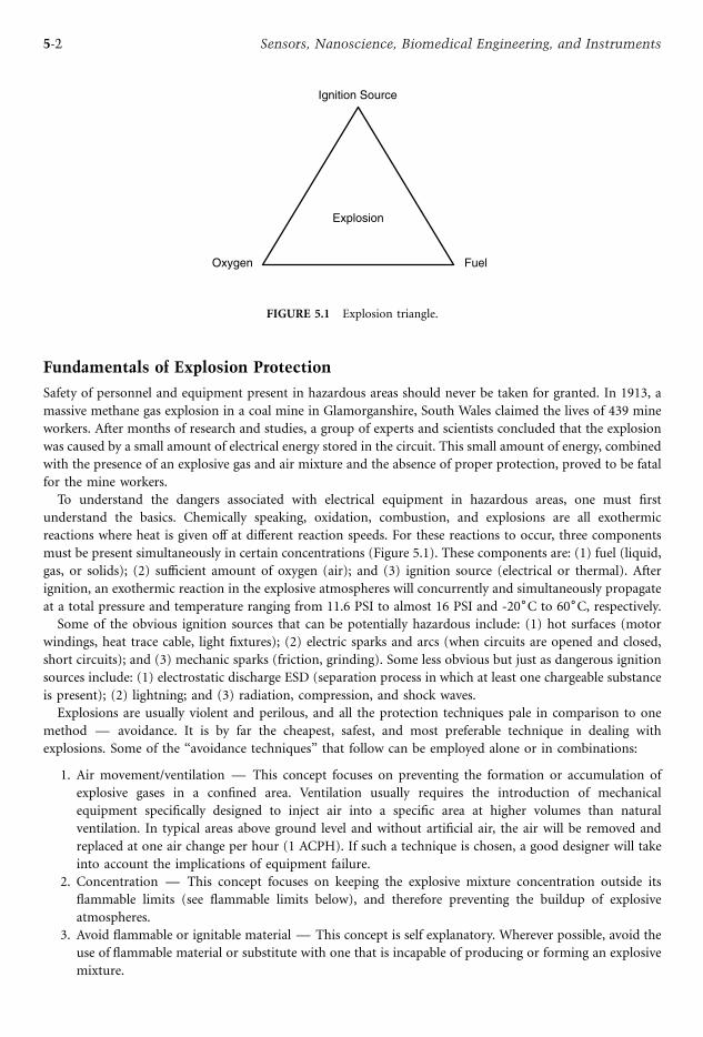
Fundamentals of Explosion Protection
Safety of personnel and equipment present in hazardous areas should never be taken for granted. In 1913, a
massive methane gas explosion in a coal mine in Glamorganshire, South Wales claimed the lives of 439 mine
workers. After months of research and studies, a group of experts and scientists concluded that the explosion
was caused by a small amount of electrical energy stored in the circuit. This small amount of energy, combined
with the presence of an explosive gas and air mixture and the absence of proper protection, proved to be fatal
for the mine workers.
To understand the dangers associated with electrical equipment in hazardous areas, one must first
understand the basics. Chemically speaking, oxidation, combustion, and explosions are all exothermic
reactions where heat is given off at different reaction speeds. For these reactions to occur, three components
must be present simultaneously in certain concentrations (Figure 5.1). These components are: (1) fuel (liquid,
gas, or solids); (2) sufficient amount of oxygen (air); and (3) ignition source (electrical or thermal). After
ignition, an exothermic reaction in the explosive atmospheres will concurrently and simultaneously propagate
at a total pressure and temperature ranging from 11.6 PSI to almost 16 PSI and -20–C to 60–C, respectively.Some of the obvious ignition sources that can be potentially hazardous include: (1) hot surfaces (motor
windings, heat trace cable, light fixtures); (2) electric sparks and arcs (when circuits are opened and closed,
short circuits); and (3) mechanic sparks (friction, grinding). Some less obvious but just as dangerous ignition
sources include: (1) electrostatic discharge ESD (separation process in which at least one chargeable substance
is present); (2) lightning; and (3) radiation, compression, and shock waves.
Explosions are usually violent and perilous, and all the protection techniques pale in comparison to one
method — avoidance. It is by far the cheapest, safest, and most preferable technique in dealing with
explosions. Some of the ‘‘avoidance techniques’’ that follow can be employed alone or in combinations:
1. Air movement/ventilation — This concept focuses on preventing the formation or accumulation of
explosive gases in a confined area. Ventilation usually requires the introduction of mechanical
equipment specifically designed to inject air into a specific area at higher volumes than natural
ventilation. In typical areas above ground level and without artificial air, the air will be removed and
replaced at one air change per hour (1 ACPH). If such a technique is chosen, a good designer will take
into account the implications of equipment failure.
2. Concentration — This concept focuses on keeping the explosive mixture concentration outside its
flammable limits (see flammable limits below), and therefore preventing the buildup of explosive
atmospheres.
3. Avoid flammable or ignitable material — This concept is self explanatory. Wherever possible, avoid the
use of flammable material or substitute with one that is incapable of producing or forming an explosive
mixture.
Explosion
Oxygen Fuel
Ignition Source
FIGURE 5.1 Explosion triangle.
5-2 Sensors, Nanoscience, Biomedical Engineering, and Instruments
4. Adjusting the flash point (see definition below) — Raising the flash point temperature of the flammable
substance usually does the trick. For a water soluble mixture, this can be easily achieved by adding water.
5. Oxygen starvation — This concept focuses on limiting the oxygen to less than 10% of volume. This is
usually accomplished by introducing a high volume of what is commonly known as inert gases, such as
nitrogen, to themixture causing the ratio of inert gas to explosivemixture to exceed 25 to 1. At such a ratio,
the buildup of explosive concentration is virtually impossible regardless the volume of air (oxygen) added.
When dealing with electrical equipment in hazardous locations, it is important to understand the following
terms as they are use frequently when it comes to hazardous areas
1. Flash Point (FP) — The minimum temperature at normal air pressure at which a combustible or
flammable material releases sufficient vapors ignitible by an energy source. FP provides an indication of
how easily a chemical may burn. The lower the FP, the greater the hazard. Depending on the flash point,
flammable liquids are divided into four classes of hazard: (1) AI (FP , 21–C), (2) AII
(21 , FP , 55–C), (3) AIII (55–C , FP , 100–C), and (4) B (FP , 21–C at 15–C dissolving in
water).
2. Flammable Liquids — Are generally volatile and give off vapors with vapor density over 1.0, and
therefore collect at low points. They also have a flash point below 100–F (37.8–C) with a vapor pressurebelow 40 PSI.
3. Combustible Liquids — Have most of the characteristics of flammable liquids, except that their flash
point is above 100–F (37.8–C).4. Ignition Temperature — The minimum temperature under normal operating pressure at which a
dangerous mixture ignites independently of the heating or heated element.
5. Flammable Limits (FL) — The upper flammable limit (UFL), also known as the upper explosive limit
(UEL), or the maximum concentration ratio of vapor to air mixture above which the propagation of
flame does not occur when exposed to an ignition source. Here, the mixture is said to be ‘‘too rich’’ to
burn. The lower flammable limit (LFL), also know as lower explosive limit (LEL), is the minimum
concentration ratio of vapor to air mixture below which the propagation of flame does not occur when
exposed to an ignition source. Also, here, the mixture is said to be ‘‘too lean’’ to explode. Significant
attention must be given to LEL, since it provides the minimum quantity of gas necessary to create a
hazardous mixture. Generally, the flammable limits are indicated in percent by volume, which is
abbreviated % vol. Note that the explosion of a mixture in the middle the of UEL and LEL is much more
violent than if the mixture were closer to either limit.
6. Maximum Surface Temperature — The maximum temperature generated by a piece of electrical
equipment under normal or fault conditions. This temperature must be below the minimum ignition
temperature of the potentially explosive surrounding atmosphere. Equipment used in hazardous
locations must be clearly marked to indicate class, group, and maximum surface temperature or range
referenced to 40–C (104–F) ambient temperature. Table 5.1 shows that an apparatus with a specific ‘‘T’’class can be used in the presence of all gases having an ignition temperature higher than the ‘‘T’’
temperature class of the device. For added safety, it is recommended that the maximum surface
temperature be not more than 80% of the minimum ignition temperature of the surrounding gas. The
reader is cautioned not to confuse maximum working (operating) temperature with maximum surface
temperature, which is measured under worst-case conditions of the electrical apparatus. An electrical
apparatus designed to operate with a maximum ambient temperature of 70–C — even in the worst
conditions of the expected temperature range — must not have a temperature rise greater than a safety
margin of 10–C to be classified as T6 or 5–C for classes T3, T4, and T5 (Table 5.1).
7. Vapor Density — The weight of a volume of pure vapor gas compared to the weight of an equal volume
of dry air under the same normal atmospheric pressure and temperature. It is calculated as the ratio of
molecular weight of the gas to the average molecular weight of air (28.96). Methane gas (CH4) with
molecular weight of 16 and vapor density of 0.6 tends to rise, while Acetone (C3H6O) with molecular
weight of 58 and vapor density of 2 tends to settle closer to ground levels. A vapor density of 0.75 is
typically considered the limit between lighter and heavier gases.
5-3Instruments and Measurements

8. Air Current and Ventilation — Air movement/current can be both helpful and disastrous. A strong air
movement/current can help dilute the gas concentration and consequently reduce, if not eliminate the
hazard. A soft air movement/current can easily extend the perimeter of the hazardous area into an
adjacent safe area.
9. Vapor Dispersion — Where solid boundaries (walls, enclosures, panels, etc.) do not exist, vapor
dispersion will depend predominately on gas vapor density and velocity. Lighter vapors tend to disperse
vertically and outward, while heavier vapors tend to settle downward and out.
10. Fuels — Fuels of all forms — solid, liquid, and gas — are chemical substances that may be burned
in oxygen to generate heat, and are made up predominately of carbon and hydrogen and occasionally
sulfur. The ingredients of a combustion process are called reactants, while the outputs are called products.
Hazardous Areas Classification
In the United States, the National Electrical Code (NEC) defines a hazardous area as ‘‘an area where a potential
hazard may exist under normal or abnormal conditions because of the presence of flammable, combustible, or
ignitible materials.’’ This general description is divided into different classes, divisions, and groups to properly
assess the extent of the hazard and to design and specify safe operating electrical systems.
The need for classification is important not only for safety, but for economic reasons as well. Proper
application, good engineering, and experience can reduce the extent of the most volatile areas (Class I,
Division 1) within reasonably safe distances of potential leaks and ignition sources. Under Class I, Division 1,
equipment and installation costs can become an economic burden because the equipment is considerably
more expensive and must pass stringent tests to ensure proper and safe operation under normal or abnormal
conditions. The National Fire Protection Association (NFPA 497 A & B) and the American Petroleum
Institutes ‘‘Recommended Practice for Classification of Locations for Electrical Installations at Petroleum
Facilities’’ (ANSI/API RP 500) are excellent resources for defining hazardous area boundaries.
Classification of a hazardous area within a facility is usually determined by highly-qualified personnel,
including chemical engineers, process engineers, and safety officers. Their primary objective is to determine
where a potentially hazardous atmosphere exists, under what conditions it exists, and how long it exists.
Careful study and design of electrical installations, especially in hazardous areas, are crucial for the safe
operation of electrical equipment and prevention of an accidental ignition of flammable materials. The NEC,
TABLE 5.1 Maximum Surface Temperature under All Operating Conditions
Maximum Temperature
–C –F Identification Number
450 842 T1
300 572 T2
280 536 T2A
260 500 T2B
230 446 T2C
215 419 T2D
200 392 T3
180 356 T3A
165 329 T3B
160 320 T3C
135 275 T4
120 248 T4A
100 212 T5
85 185 T6
Note: Surface temperature of electric apparatus during operation must not exceedlimitations of the hazard present. Reprinted with permission from NEPA 70-1996, theNational Electrical Code1, Copyright# 1995, National Free Protection Association,Quincy, MA. This reprinted Protection Association, on the referenced subject which isrepresented only by the standard in its entirety.
5-4 Sensors, Nanoscience, Biomedical Engineering, and Instruments
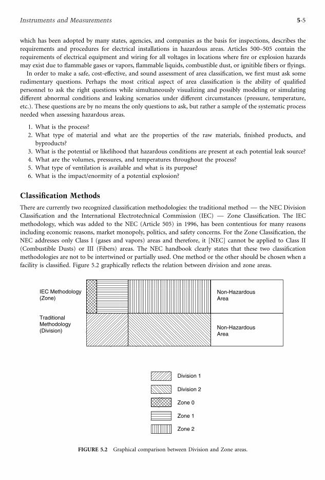
which has been adopted by many states, agencies, and companies as the basis for inspections, describes the
requirements and procedures for electrical installations in hazardous areas. Articles 500–505 contain the
requirements of electrical equipment and wiring for all voltages in locations where fire or explosion hazards
may exist due to flammable gases or vapors, flammable liquids, combustible dust, or ignitible fibers or flyings.
In order to make a safe, cost-effective, and sound assessment of area classification, we first must ask some
rudimentary questions. Perhaps the most critical aspect of area classification is the ability of qualified
personnel to ask the right questions while simultaneously visualizing and possibly modeling or simulating
different abnormal conditions and leaking scenarios under different circumstances (pressure, temperature,
etc.). These questions are by no means the only questions to ask, but rather a sample of the systematic process
needed when assessing hazardous areas.
1. What is the process?
2. What type of material and what are the properties of the raw materials, finished products, and
byproducts?
3. What is the potential or likelihood that hazardous conditions are present at each potential leak source?
4. What are the volumes, pressures, and temperatures throughout the process?
5. What type of ventilation is available and what is its purpose?
6. What is the impact/enormity of a potential explosion?
Classification Methods
There are currently two recognized classification methodologies: the traditional method — the NEC Division
Classification and the International Electrotechnical Commission (IEC) — Zone Classification. The IEC
methodology, which was added to the NEC (Article 505) in 1996, has been contentious for many reasons
including economic reasons, market monopoly, politics, and safety concerns. For the Zone Classification, the
NEC addresses only Class I (gases and vapors) areas and therefore, it [NEC] cannot be applied to Class II
(Combustible Dusts) or III (Fibers) areas. The NEC handbook clearly states that these two classification
methodologies are not to be intertwined or partially used. One method or the other should be chosen when a
facility is classified. Figure 5.2 graphically reflects the relation between division and zone areas.
Division 1
Division 2
Zone 0
Zone 1
Zone 2
IEC Methodology(Zone)
TraditionalMethodology(Division)
Non-HazardousArea
Non-HazardousArea
FIGURE 5.2 Graphical comparison between Division and Zone areas.
5-5Instruments and Measurements

Division Classification
In North America, hazardous areas are separated by classes, divisions, and groups. Article 500 of the NEC and
Table 5.2 describe hazardous locations by Class, Division, and Group. The Class defines the physical form of
combustible material mixed with oxygen molecules. The Division defines the probability of an explosive fuel
to air mixture being present. The Group indicates the type of vapor or dust present. The NEC gives the
following definitions:1
Class I, Division 1 Locations
1. Where ignitible concentrations of flammable gases or vapors can exist under normal operating
conditions; may exist frequently because of repair or maintenance operations or because of leakage; and
where breakdown or faulty operation of equipment or processes might release ignitible concentrations of
flammable gases or vapors, and cause simultaneous failure of electric equipment.
Class I, Division 2 Locations
1. Where volatile flammable liquids or flammable gases are handled, processed, or used but where the
liquids, vapors, or gases will normally be confined within closed containers or closed systems from
which they can escape only in case of accidental rupture or breakdown of such containers or systems, or
in case of abnormal operation of equipment;
2. Where ignitible concentrations of gases or vapors are normally prevented by positive mechanical
ventilation, and where they might become hazardous through failure or abnormal operation of the
ventilating equipment;
3. Adjacent to Class I, Division 1 locations, and where ignitible concentrations of gases or vapors might
occasionally be communicated; unless such communication is prevented by positive-pressure ventilation
from a source of clean air, and effective safeguards against ventilation failure are provided.
1Reprinted with permission from NFPA 70–2005, National Electrical Code1, Copyright# 2004, National Fire Protection
Association. This reprinted material is not the complete and official position of the NFPA, on the referenced subject which is
represented only by the standard in its entirety. National Electrical Code1 and NEC1 are registered trademarks of the National
Fire Protection Association, Inc., Quincy, MA 02169.
TABLE 5.2 Area Classification Based on NEC
Division 1—Hazard Is Present under Normal
Operating Conditions
Class I Gases and Vapor
Group A e.g., Acetylene
Group B e.g., Hydrogen
Group C e.g., ethylene
Group D e.g., methane
Class II Combustible dusts
Group E Metal dust
Group F Coal dust
Group G Grain dust
Class III Fibers
Division 2—Hazard Is Present only
under Abnormal Operating Conditions
5-6 Sensors, Nanoscience, Biomedical Engineering, and Instruments

Class II, Division 1 Locations
1. Where combustible dust is in the air under normal operation conditions in quantities sufficient to
produce explosive or ignitible mixtures;
2. Where mechanical failure or abnormal operation of machinery or equipment might cause such explosive
or ignitible mixtures to be produced, and also might provide a source of ignition through simultaneous
failure of electric equipment, operation of protective devices, or from other causes;
3. Where combustible dusts of an electrically conductive nature may be present in hazardous quantities.
Class II, Division 2 Locations
Where combustible dust normally is not in the air in quantities sufficient to produce explosive or
ignitible mixtures, and dust accumulations normally are insufficient to interfere with the safe dissipation
of heat from electrical equipment, or may be ignitible by abnormal operation or failure of electrical equipment.
Class III, Division 1 Locations
Where easily ignitible fibers or materials producing combustible flyings are handled, manufactured, or used.
Class III, Division 2 Locations
Where easily ignitible fibers are stored or handled. Quantities and properties of hazardousmaterials are the basis
upon which the NEC classifies hazardous locations. Each hazardous location must be evaluated carefully to
determine the appropriate classification to facilitate the design process and to help specify the correct equipment.
Marking
All equipment used in hazardous area must be clearly marked to reflect class, group and operating
temperature referenced to 40–C (104–F) or temperature class (e.g. Class I, Division 1, Group D, T6).
Sometime, Division (or Div.) is not shown on the equipment nameplate, such equipment not marked to
indicate division or marked ‘‘Division 1’’ or ‘‘Div.1’’ can be used in both Division 1&2 locations. However,
equipment marked ‘‘Division 2’’ or ‘‘Div 2’’ can only be used in Division 2. locations. If temperature class is
used it shall indicate the ‘‘T Code’’ referenced in Table 5.1. Some equipment is provided with thermally
protected (TP) sensors, designed specifically to limit the temperature to that marked one on the equipment.
Without such TPs, operating these equipment in an ambient temperature higher than 40–C (104–F), willincrease the operating temperature of the equipment. Equipment marked for use in Class I and II, shall be
marked with the maximum safe operating temperature, based on simultaneous exposure to the combination
of Class I and Class II conditions.
Zone Classification
In Europe and countries (outside of North America), classification of hazardous areas is accomplished-
differently. BS EN 60079–10 is the standard for determining the classification of hazardous areas, giving
guidance in determining the area classification and recommendations for detailing the zones on drawings.
The standard also gives details about the protective measures that need to be applied to reduce the risk of
explosions. In the United States, Article 505 of the NEC describes hazardous locations by Class, Zone, and
Group. The Class defines the physical form of combustible material mixed with oxygen molecules. The Zone
classification defines the probability of an explosive fuel to air mixture being present. The Group indicates
the type of vapor or dust present. Table 5.3a defines area classification under the IEC methodology and
compares it to the Division methodology. The zone classification is defined by the IEC. Hazardous locations
are classified depending on the properties of the flammable vapors, liquids, or gases that may be present and
the likelihood that a flammable or combustible concentration is present. From Table 5.3a we can see that
Division 2 is equivalent to Zone 2, while Division 1 is split between Zone 1 and Zone 0. It is worth noting
that equipment approved for the Divisional area may and can be used in the equivalent Zone area. Because
of the idiosyncrasies such as supervision of work, dual classifications and area reclassification associated with
5-7Instruments and Measurements

TABLE 5.3 Division vs. Zone Comparison Based on the National Electrical Code (Traditional Method vs. IEC)
Table 3a—Area Classification Comparison
Traditional Method IEC Method
Division 1: Zone 0:
Where ignitable concentrations of
flammable gases, vapors or
liquids can exist all of the time or
some of the time
under normal operating conditions
Where ignitable concentrations of flammable
gases, vapors or liquids can exist all of the time
or for long periods of time under normal
operating conditions
Zone 1:
Where ignitable concentrations of flammable
gases, vapors or liquids can exist some of the
time under normal operating conditions
Division 2: Zone 2:
Where ignitable concentrations of
flammable gases, vapors or liquids are
not likely to exist under normal
operating conditions.
Where ignitable concentrations of flammable
gases, vapors or liquids are not likely to exist
under normal operating conditions.
Table 3b—Protection Method Comparison
Traditional Method IEC Method
Division 1: Zone 0:
Explosion proof Intrinsically safe ‘‘n’’ (2 fast)
Intrinsically safe (2 fast) Class I, Div. 1 Intrinsically safe (2 fast)
Purged pressurized (Type X or Y)
Zone 1:
Encapsulation, ‘‘m’’
Flameproof, ‘‘o’’
Increased safety, ‘e’
Intrinsically safe, ‘‘b’’ (1 fast)
Oil immersion, ‘‘o’’
Powder filling, ‘‘q’’
Purged pressurized, ‘‘p’’
Any Class I, Zone 0 method
Any Class I, Div. 1 method
Division 2: Zone 2:
Hermetically sealed Hermetically sealed, ‘‘nC’’
Nonincentive Nonincentive ‘‘nC’’
Non-sparking Non-sparking, ‘‘nA’’
Oil immersion Restricted breathing, ‘‘nR’’
Purge pressurized (Type Z) Sealed device, ‘‘nC’’
Sealed device Any Class I, Zone 0 or 1 method
Any Class I Div. 1 method Any Class I, Div. 1 or 2 method
Table 3c—Temperature Code Comparison
Traditional Method IEC Method
T1 450–C/842–F T1
T2 300–C/572–F T2
T2A 250–C/536–F –
T2B 260–C/500–F –
T2C 230–C/446–F –
T2D 215–C/419–F –
T3 200–C/392–F T3
T3A 180–C/356–F –
T3B 165–C/329–F –
T3C 160–C/320–F –
5-8 Sensors, Nanoscience, Biomedical Engineering, and Instruments

Zone Classification, it is usually used in new construction or areas requiring major process and upgrades.
Zone classification is divided into six categories:
Zone 0 Locations
Where ignitable concentrations of flammable gases, vapors or liquids can exist all of the time or for long
periods of time under normal operating conditions.
Zone 1 Locations
Where ignitable concentrations of flammable gases, vapors or liquids can exist some of the time under normal
operating conditions
Zone 2 Locations
Where ignitable concentrations of flammable gases, vapors or liquids are not likely to exist under normal
operating conditions.
Zone 20 Locations
Where an explosive atmosphere in the form of a cloud of combustible dust in air is present continuously, or
for long periods or frequently.
Zone 21 Locations
Where an explosive atmosphere in the form of a cloud of combustible dust in air is likely to occur in normal
operation occasionally.
Zone 22 Locations
Where an explosive atmosphere in the form of a cloud of combustible dust in air is not likely to occur in
normal operation but, if it does occur, will persist for a short period only.
Marking
As with division marking, all equipment used in hazardous area must be marked to reflect five points that
must be clearly shown in order on the equipment nameplate:
TABLE 5.3 (Continued)
Traditional Method IEC Method
T4 135–C/275–F T4
T4A 120–C/248–F –
T5 100–C/212–F T5
T6 85–C/185–F T6
Table 3d—Gas Group Comparison
Traditional Method IEC Method
A (acetylene) IIC (acetylene & hydrogen)
B (hydrogen) IIC (acetylene & hydrogen)
C (ethylene) IIB (ethylene)
D (propane) IIA (propane)
Table 3e—Marking Comparison
Traditional Method IEC Method
Divisions 1 or 2 Zones 0, 1 or 2
Gas Groups A, B, C or D Gas Groups IIA, B, or IIC
Temperature Codes T1-T6 Temperature Codes T1-T6
5-9Instruments and Measurements
1. Class I, Zone 1: Indicates area classification
2. AEx: Indicates equipment built to US standards (EEx for Europe)
3. ia: Indicates protection methodologies
4. IIB: Indicates gas group
5. T4 : Indicates temperature classification
Enclosure Types and Requirements
When it comes to choosing the right enclosure to house electrical equipment, this task must not be taken
lightly. Choosing the proper type of enclosure for electrical equipment is important for two reasons:
1. Personnel protection against accidental contact with enclosed electrical equipment.
2. Protection of internal equipment against outside harm.
Enclosures are designated by a type number indicating the degree of protection and the condition for which
they are suitable. In some applications, enclosures have a dual purpose and therefore, are designated by a two-
part type number shown with the smaller number first (e.g., 7/9). The following enclosure types, with their
enclosed equipment, have been evaluated in accordance with Underwriters Laboratories, Inc. UL 698,
‘‘Industrial Control Equipment for Use in Hazardous Locations,’’ and are marked to show the class and group
letter designations.
Type 7 Enclosures
Type 7 enclosures are non-ventilated, intended for indoor applications, and classified for Class I, Group A, B,
C, and D as defined in Table 5.2. The letters A-D sometimes appear as a suffix to the designation Type 7 to give
the complete designation. According to UL 698, Type 7 enclosures must be designed to withstand an internal
explosion pressure of specific gases and to prevent such an explosion from igniting a hazardous mixture
outside the enclosure (Explosion Test). In addition, Type 7 enclosures fabricated from sheet steel are designed
to withstand two times the internal explosion pressure for 1 minute without permanent deformation and three
times the explosion pressure without rupture. If constructed of cast iron, the enclosure must be capable of
withstanding four times the explosion pressure without rupture or deformation. This test may be waived if
calculations show a safety factor of five to one for cast metal or four to one for fabricated steel. The enclosed
heat generating devices are specifically designed to prevent external surfaces from reaching temperatures
capable of igniting explosive vapor-air mixtures outside the enclosure (Temperature Test).
Type 8 Enclosures
Type 8 enclosures are non-ventilated, intended for indoor applications, and intended for Class I, Group A, B, C,
and D as outlined in Table 5.2. The letters A-D appear as a suffix to the designation Type 8 to give the complete
designation. According toUL 698, the oil-immersed equipmentmust be able to operate at rated voltage andmost
severe current conditions in the presence of flammable gas-air mixtures without igniting these mixtures.
Type 9 Enclosures
Type 9 enclosures are non-ventilated, intended for indoor applications, and classified for Class II, Group E, F,
and G as outlined in Table 5.2. The letters E, F, or G appear as a suffix to the designation Type 9 to give the
complete designation. According to UL 698, the enclosure with its enclosed equipment is evaluated in
accordance with UL 698 in effect at the time of manufacture. This evaluation includes a review of dimensional
requirements for shaft opening and joints, gaskets material, and temperature rise under a blanket of dust. The
device is operated at full rated load until equilibrium temperatures are reached, and then allowed to cool to
ambient temperature over a period of at least 30 hours while continuously subjected to circulating dust of
specified properties. No dust shall enter the enclosure (Dust Penetration Test). Furthermore, Type 9 enclosures
must also pass the ‘‘Temperature Test with Dust Blanket,’’ which is similar to the temperature rise test except
the circulating dust is not aimed directly at the device during testing. The dust in contact with the enclosure
shall not ignite or discolor from heat, and the exterior surface temperature based on 40–C (104–F) shall notexceed specific temperatures under normal or abnormal conditions. Where gasketed enclosures are used,
5-10 Sensors, Nanoscience, Biomedical Engineering, and Instruments

gaskets shall be of a noncombustible, non-deteriorating, vermin-proof material and shall be mechanically
attached. Type 9 ventilated enclosures are the same as non-ventilated enclosures, except that ventilation is
provided by forced air from a source outside the hazardous area to produce positive pressure within the
enclosure. The enclosure must also meet temperature design tests.
Type 10 Enclosures
Type 10 enclosures are non-ventilated and designed to meet the requirements of the U.S. Bureau of
Mines which relate to atmospheres containing mixtures of methane and air, with or without coal dust present.
It is important to note that enclosures for hazardous applications are designed for specific applications
and must be installed and maintained as recommended by the enclosure manufacturer. Any misapplication
or alteration to the enclosure may jeopardize its integrity and may eventually cause catastrophic failure of the
system. All enclosures should be solidly grounded and properly labeled with a warning sign reminding
the operator of the importance of de-energizing the incoming power to the enclosure prior to its servicing.
Protection Methodologies
Choosing a protection technique that suits each application can appear complicated because safety, reliability,
cost, and maintenance factors all must be considered. Over the years, a few hazardous area safety protection
methodologies have been used. Although methodologies differ in application and principles of operation, they
all have one common goal: to eliminate one or more components necessary for combustion. There are
different methods used in hazardous area protection environment protection. A good hazardous area assessor
recognizes that no one method alone is sufficient or suitable for all installations because of specifications and
regulatory issues. The final design is usually a combination of different methodologies designed to meet the
hazardous area specific needs. The protection methodologies can be separated into two categories:
Most widely used and popular methods include:
1. Intrinsic Safety
2. Explosion-Proof
3. Dust Ignition-Proof
4. Purging and Pressurization
Less popular methods include:
1. Powder (Sand) Filled
2. Oil Immersed
3. Non Sparking
4. Encapsulation
5. Increased Safety
6. Combustible Gas Detection System
Intrinsic Safety ‘‘i’’
Simply stated, intrinsic safety (IS) is all about preventing explosions. Intrinsic safety is based on the principle
of limiting the thermal and electrical energy levels in the hazardous area to levels that cannot cause an ignition
of a specific hazardous mixture in its most ignitable concentration. Under normal or abnormal operating
conditions (fault conditions are expected and are the essence of design for IS systems), the energy levels and
power generated are never sufficient to cause explosion by igniting a specific hazardous mixture present. IS can
only be used on instruments, control and sensing circuits where the voltage is typically 24VDC and less than
100mA. Intrinsic safety pertains to the minimum ignition temperature and the minimum ignition electrical
energy required causing a specific group to ignite. The energy level provided by an IS circuit is low (< 1 W)
and is used only to power up instruments with a low energy demand. An IS circuit incorporates an
Intrinsically Safe Apparatus (field device), and Associated Apparatus, and interconnecting wiring system.
Designing intrinsically safe systems begins with studying the field device. This will help determine the type of
5-11Instruments and Measurements
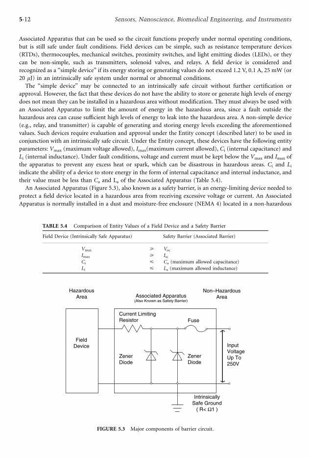
Associated Apparatus that can be used so the circuit functions properly under normal operating conditions,
but is still safe under fault conditions. Field devices can be simple, such as resistance temperature devices
(RTDs), thermocouples, mechanical switches, proximity switches, and light emitting diodes (LEDs), or they
can be non-simple, such as transmitters, solenoid valves, and relays. A field device is considered and
recognized as a ‘‘simple device’’ if its energy storing or generating values do not exceed 1.2 V, 0.1 A, 25 mW (or
20 mJ) in an intrinsically safe system under normal or abnormal conditions.
The ‘‘simple device’’ may be connected to an intrinsically safe circuit without further certification or
approval. However, the fact that these devices do not have the ability to store or generate high levels of energy
does not mean they can be installed in a hazardous area without modification. They must always be used with
an Associated Apparatus to limit the amount of energy in the hazardous area, since a fault outside the
hazardous area can cause sufficient high levels of energy to leak into the hazardous area. A non-simple device
(e.g., relay, and transmitter) is capable of generating and storing energy levels exceeding the aforementioned
values. Such devices require evaluation and approval under the Entity concept (described later) to be used in
conjunction with an intrinsically safe circuit. Under the Entity concept, these devices have the following entity
parameters: Vmax (maximum voltage allowed), Imax(maximum current allowed), Ci (internal capacitance) and
Li (internal inductance). Under fault conditions, voltage and current must be kept below the Vmax and Imax of
the apparatus to prevent any excess heat or spark, which can be disastrous in hazardous areas. Ci and Liindicate the ability of a device to store energy in the form of internal capacitance and internal inductance, and
their value must be less than Ca and La of the Associated Apparatus (Table 5.4).
An Associated Apparatus (Figure 5.3), also known as a safety barrier, is an energy-limiting device needed to
protect a field device located in a hazardous area from receiving excessive voltage or current. An Associated
Apparatus is normally installed in a dust and moisture-free enclosure (NEMA 4) located in a non-hazardous
FieldDevice
ZenerDiode
ZenerDiode
Current LimitingResistor Fuse
HazardousArea Associated Apparatus
(Also Known as Safety Barrier)
Non–HazardousArea
InputVoltageUp To250V
IntrinsicallySafe Ground
( R< Ω1 )
FIGURE 5.3 Major components of barrier circuit.
TABLE 5.4 Comparison of Entity Values of a Field Device and a Safety Barrier
Field Device (Intrinsically Safe Apparatus) Safety Barrier (Associated Barrier)
Vmax > VocImax > IscCi < Ca (maximum allowed capacitance)
Li < La (maximum allowed inductance)
5-12 Sensors, Nanoscience, Biomedical Engineering, and Instruments
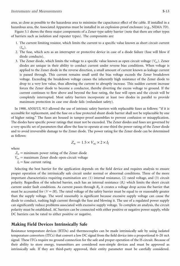
area, as close as possible to the hazardous area to minimize the capacitance effect of the cable. If installed in a
hazardous area, the Associated Apparatus must be installed in an explosion-proof enclosure (e.g., NEMA 7D).
Figure 5.1 shows the three major components of a Zener-type safety barrier (note that there are other types
of barriers such as isolation and repeater types). The components are:
1. The current limiting resistor, which limits the current to a specific value known as short circuit current
(Isc).
2. The fuse, which acts as an interrupter or protective device in case of a diode failure (fuse will blow if
diode conducts).
3. The Zener diode, which limits the voltage to a specific value known as open circuit voltage (Voc). Zener
diodes are unique in their ability to conduct current under reverse bias conditions. When voltage is
applied to the Zener diode in the reverse direction, a small amount of current known as leakage current
is passed through. This current remains small until the bias voltage exceeds the Zener breakdown
voltage. Exceeding the breakdown voltage causes the inherently high resistance of the Zener diode to
drop to a very low value, thus allowing the current to abruptly increase. This sudden current increase
forces the Zener diode to become a conductor, thereby diverting the excess voltage to ground. If the
current continues to flow above and beyond the fuse rating, the fuse will open and the circuit will be
completely interrupted. Most safety barriers incorporate at least two diodes in parallel to provide
maximum protection in case one diode fails (redundant safety).
In 1988, ANSI/UL 913 allowed the use of intrinsic safety barriers with replaceable fuses as follows: ‘‘if it is
accessible for replacement, and the fuse on a fuse protected shunt diode barrier shall not be replaceable by one
of higher rating.’’ The fuses are housed in tamper-proof assemblies to prevent confusion or misapplication.
The diodes have specific power ratings that must not be exceeded. The Zener diodes and fuses are governed by
a very specific set of parameters that allow the fuse to operate at one-third the power rating of the Zener diode
and to avoid irreversible damage to the Zener diode. The power rating for the Zener diode can be determined
as follows:
Zw ¼ 1:5 · Voc · 2 · Ifwhere
Zw ¼minimum power rating of the Zener diode
Voc ¼maximum Zener diode open-circuit voltage
If ¼ fuse current rating
Selecting the best barrier for the application depends on the field device and requires analysis to ensure
proper operation of the intrinsically safe circuit under normal or abnormal conditions. Three of the more
important characteristics requiring examination are: (1) internal resistance, (2) rated voltage, and (3) circuit
polarity. Regardless of the selected barrier, each has an internal resistance (Ri) which limits the short circuit
current under fault conditions. As current passes through Ri, it creates a voltage drop across the barrier that
must be accounted for (V¼ IR). The rated voltage of the safety barrier must be equal to or reasonably greater
than the supply voltage. The word reasonably is significant because excessive supply voltage can cause the
diode to conduct, rushing high current through the fuse and blowing it. The use of a regulated power supply
can significantly reduce problems associated with excessive supply voltage. To complete an analysis, the circuit
polarity must be established. AC barriers can be connected with either positive or negative power supply, while
DC barriers can be rated to either positive or negative.
Making Field Devices Intrinsically Safe
Resistance temperature devices (RTDs) and thermocouples can be made intrinsically safe by using isolated
temperature converters (ITCs) that convert a low DC signal from the field device into a proportional 4–20 mA
signal. These ITCs require no ground connection for the safe and proper operation of the IS circuit. Because of
their ability to store energy, transmitters are considered non-simple devices and must be approved as
intrinsically safe. If they are third-party approved, their entity parameter must be carefully considered.
5-13Instruments and Measurements
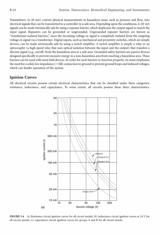
Transmitters (4–20 mA) convert physical measurements in hazardous areas, such as pressure and flow, into
electrical signals that can be transmitted to a controller in a safe area. Depending upon the conditions, 4–20 mA
signals can be made intrinsically safe by using a repeater barrier, which duplicates the output signal to match the
input signal. Repeaters can be grounded or ungrounded. Ungrounded repeater barriers are known as
‘‘transformer-isolated barriers,’’ since the incoming voltage or signal is completely isolated from the outgoing
voltage or signal via a transformer. Digital inputs, such as mechanical and proximity switches, which are simple
devices, can be made intrinsically safe by using a switch amplifier. A switch amplifier is simply a relay or an
optocoupler (a high-speed relay that uses optical isolation between the input and the output) that transfers a
discrete signal (e.g., on/off) from the hazardous area to a safe area. Grounded safety barriers are passive devices
designed specifically to prevent excessive energy in a non-hazardous area from reaching a hazardous area. These
barriers can be used with most field devices. In order for such barriers to function properly, we must emphasize
the need for a solid, low impedance (,1O) connection to ground to prevent ground loops and induced voltages,which can hinder operation of the system.
Ignition Curves
All electrical circuits possess certain electrical characteristics that can be classified under three categories:
resistance, inductance, and capacitance. To some extent, all circuits possess these three characteristics.
5A
2A
1A
500 mA
200 mA
100 mA
50 mA
20 mA
10 mA10 20 50 100 200
Source voltage (V)
Igni
tion
curr
ent(
I)
Methone
Groups D,F,G
Groups C & E
Groups A & B
(a)
FIGURE 5.4 (a) Resistance circuit ignition curves for all circuit metals; (b) inductance circuit ignition curves at 24 V for
all circuit metals; (c) capacitance circuit ignition curves for groups A and B for all circuit metals.
5-14 Sensors, Nanoscience, Biomedical Engineering, and Instruments
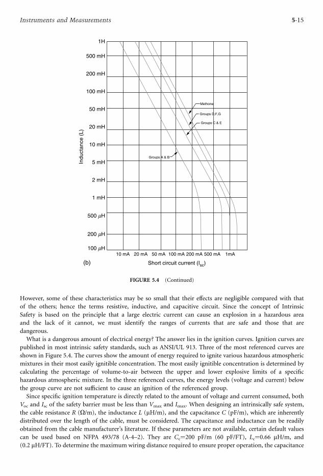
However, some of these characteristics may be so small that their effects are negligible compared with that
of the others; hence the terms resistive, inductive, and capacitive circuit. Since the concept of Intrinsic
Safety is based on the principle that a large electric current can cause an explosion in a hazardous area
and the lack of it cannot, we must identify the ranges of currents that are safe and those that are
dangerous.
What is a dangerous amount of electrical energy? The answer lies in the ignition curves. Ignition curves are
published in most intrinsic safety standards, such as ANSI/UL 913. Three of the most referenced curves are
shown in Figure 5.4. The curves show the amount of energy required to ignite various hazardous atmospheric
mixtures in their most easily ignitible concentration. The most easily ignitible concentration is determined by
calculating the percentage of volume-to-air between the upper and lower explosive limits of a specific
hazardous atmospheric mixture. In the three referenced curves, the energy levels (voltage and current) below
the group curve are not sufficient to cause an ignition of the referenced group.
Since specific ignition temperature is directly related to the amount of voltage and current consumed, both
Voc and Isc of the safety barrier must be less than Vmax and Imax. When designing an intrinsically safe system,
the cable resistance R (O/m), the inductance L (mH/m), and the capacitance C (pF/m), which are inherently
distributed over the length of the cable, must be considered. The capacitance and inductance can be readily
obtained from the cable manufacturer’s literature. If these parameters are not available, certain default values
can be used based on NFPA 493/78 (A-4–2). They are Cc¼200 pF/m (60 pF/FT), Lc¼0.66 mH/m, and(0.2 mH/FT). To determine the maximum wiring distance required to ensure proper operation, the capacitance
1H
500 mH
200 mH
100 mH
50 mH
20 mH
10 mH
5 mH
2 mH
1 mH
500 mH
200 mH
100 mH10 mA 20 mA 50 mA 100 mA 200 mA 500 mA 1mA
Short circuit current (Isc)
Indu
ctan
ce(L
)
Methone
Groups D,F,G
Groups C & E
Groups A & B
(b)
FIGURE 5.4 (Continued)
5-15Instruments and Measurements
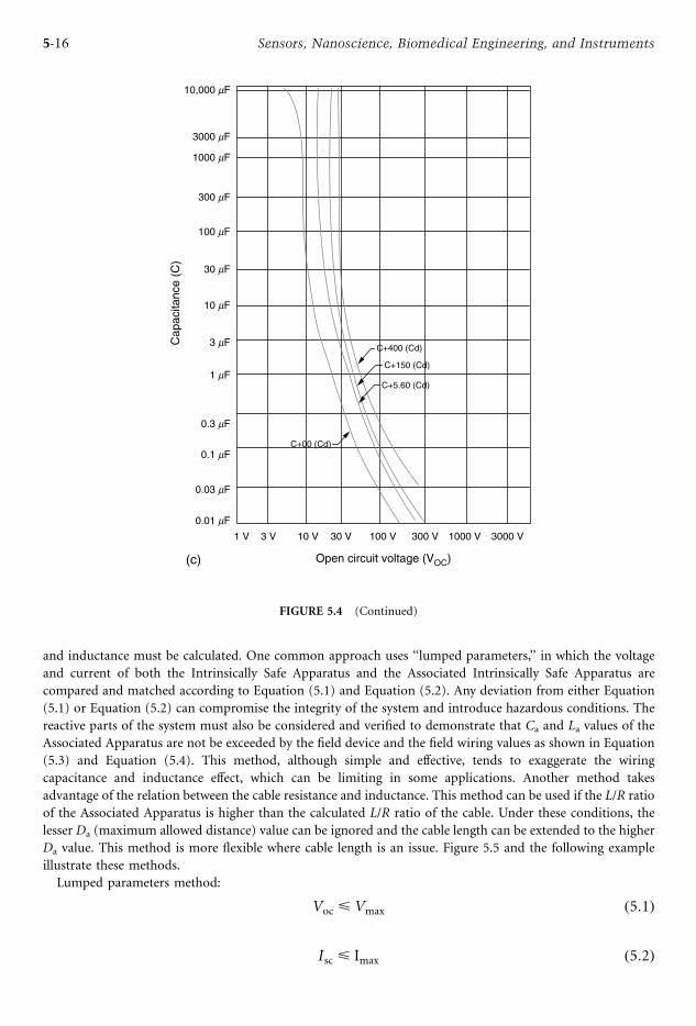
and inductance must be calculated. One common approach uses ‘‘lumped parameters,’’ in which the voltage
and current of both the Intrinsically Safe Apparatus and the Associated Intrinsically Safe Apparatus are
compared and matched according to Equation (5.1) and Equation (5.2). Any deviation from either Equation
(5.1) or Equation (5.2) can compromise the integrity of the system and introduce hazardous conditions. The
reactive parts of the system must also be considered and verified to demonstrate that Ca and La values of the
Associated Apparatus are not be exceeded by the field device and the field wiring values as shown in Equation
(5.3) and Equation (5.4). This method, although simple and effective, tends to exaggerate the wiring
capacitance and inductance effect, which can be limiting in some applications. Another method takes
advantage of the relation between the cable resistance and inductance. This method can be used if the L/R ratio
of the Associated Apparatus is higher than the calculated L/R ratio of the cable. Under these conditions, the
lesser Da (maximum allowed distance) value can be ignored and the cable length can be extended to the higher
Da value. This method is more flexible where cable length is an issue. Figure 5.5 and the following example
illustrate these methods.
Lumped parameters method:
Voc < Vmax ð5:1Þ
Isc < Imax ð5:2Þ
10,000 mF
3000 mF
1000 mF
300 mF
100 mF
30 mF
10 mF
3 mF
1 mF
0.3 mF
0.1 mF
0.03 mF
0.01 mF
Cap
acita
nce
(C)
1 V 3 V 10 V 30 V 100 V 300 V 1000 V 3000 V
Open circuit voltage (VOC)
C+400 (Cd)
C+150 (Cd)
C+5.60 (Cd)
C+00 (Cd)
(c)
FIGURE 5.4 (Continued)
5-16 Sensors, Nanoscience, Biomedical Engineering, and Instruments

Cc < Ca Ci 0:45mF 0:30mF ¼ 0:15mF ð5:3Þ
Lc < La Li 3:5mH 2:0mH ¼ 1:5mH ð5:4Þ
The maximum length of the field wiring, referred to its capacitance and inductance, is the lesser value of Da.
Da ¼ 0:15 mF=150 pF=m ¼ 1; 000m
Da ¼ 1:5mH=2:0 mH=m ¼ 750m ðmaximum distance of field wiringÞL/R ratio method:
Since the cable L/R ratio of 41.6 mH/O (2 mH/m / 48 O/km) is less than the given Associated Apparatus L/Rratio, the inductive effect can be ignored and the maximum distance can be increased to 1,000 m.
Certification and Approval
Although approval and certification processes help to provide safety, careful planning, designing, and
engineering are still necessary. Intrinsic safety standards, procedures, and tests are recognized worldwide.
Testing authorities include Underwriters Laboratories Inc. (UL) and Factory Mutual Research Corp. (FM) in
the United States, Canadian Standards Association (CSA) in Canada, and Physikalisch-Technische
Bundesanstalt (PTB) in Europe. Intrinsically safe products are suitable for all Classes, Divisions, and Groups
outlined in Table 5.2. It is imperative that the Intrinsically Safe product must be rated and classified for each
specific application (zone/class, division and group). Since air is made up of 79% nitrogen and 21% oxygen, IS
approvals are based on 21% oxygen concentration. A typical UL label identifies that the device is suitable for
intrinsic safe application in specific Zone/Class, Division and Group. A 21% oxygen concentration is common
within the industry and the approving agencies that test and certify instruments as intrinsically safe for normal
oxygen concentration. Oxygen concentration can vary; depending on the situation certain conditions can exist
well over 21% causing what is commonly called an ‘‘enriched environment’’ and can consequently increase the
risk of flammability.
In the United States, FM adopted two methods for testing and approving equipment to be used in
hazardous areas:
1. Loop (System) Approval — Where an Intrinsically Safe Apparatus is evaluated in combination with a
specific Associated Apparatus and is approved to be installed in this manner. Any changes to the circuit
require re-evaluation and certification (Figure 5.6).
Hazardous Area Non–Hazardous Area
Intrinsically
Safe
Apparatus
Field Wiring Associated
Intrinsically
Safe
Apparatus
Vmin = 12 V Voc = 24 V
Isc = 0.3 A
La = 3.5 mH
L\R = 60 mH/Ω
Vmax = 30 V
Imax = 0.5 A
Ci = 0.3 mFCa = 0.45 mF
Li = 2.0 mH
C = 150 pF/m
L = 2.0 mH/m
R = 48 Ω/km
FIGURE 5.5 Analysis of an intrinsically safe system.
5-17Instruments and Measurements
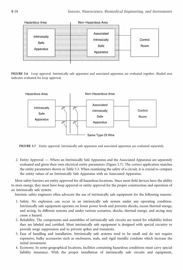
2. Entity Approval — Where an Intrinsically Safe Apparatus and the Associated Apparatus are separately
evaluated and given their own electrical entity parameters (Figure 5.7). The correct application matches
the entity parameters shown in Table 5.3. When examining the safety of a circuit, it is crucial to compare
the entity values of an Intrinsically Safe Apparatus with an Associated Apparatus.
Most safety barriers are entity approved for all hazardous locations. Since most field devices have the ability
to store energy, they must have loop approval or entity approval for the proper construction and operation of
an intrinsically safe system.
Intrinsic safety engineers often advocate the use of intrinsically safe equipment for the following reasons:
1. Safety. No explosion can occur in an intrinsically safe system under any operating condition.
Intrinsically safe equipment operates on lower power levels and prevents shocks, excess thermal energy,
and arcing. In different systems and under various scenarios, shocks, thermal energy, and arcing may
cause a hazard.
2. Reliability. The components and assemblies of intrinsically safe circuits are tested for reliability before
they are labeled and certified. Most intrinsically safe equipment is designed with special circuitry to
provide surge suppression and to prevent spikes and transients.
3. Ease of handling and installation. Intrinsically safe systems tend to be small and do not require
expensive, bulky accessories such as enclosures, seals, and rigid metallic conduits which increase the
initial investment.
4. Economy. In some geographical locations, facilities containing hazardous conditions must carry special
liability insurance. With the proper installation of intrinsically safe circuits and equipment,
FIGURE 5.6 Loop approval. Intrinsically safe apparatus and associated apparatus are evaluated together. Shaded area
indicates evaluated for loop approval.
Same Type Of Wire
Hazardous Area Non–Hazardous Area
Control
Room
Intrinsically
Safe
Apparatus
Associated
Intrinsically
Safe
Apparatus
FIGURE 5.7 Entity approval. Intrinsically safe apparatus and associated apparatus are evaluated separately.
5-18 Sensors, Nanoscience, Biomedical Engineering, and Instruments
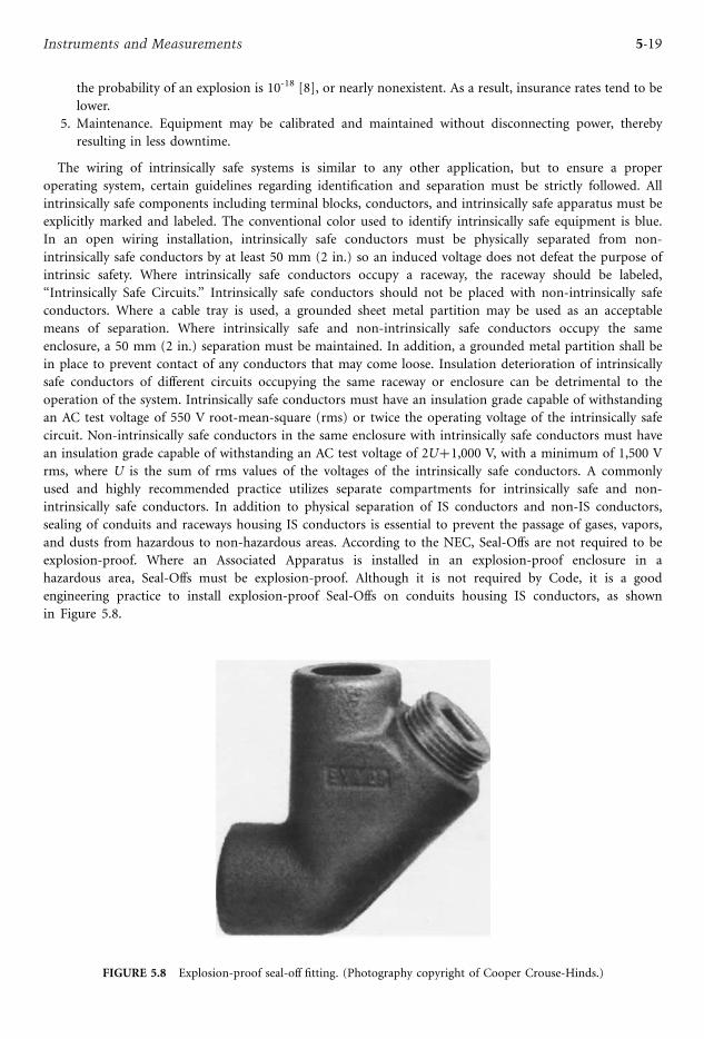
the probability of an explosion is 10-18 [8], or nearly nonexistent. As a result, insurance rates tend to be
lower.
5. Maintenance. Equipment may be calibrated and maintained without disconnecting power, thereby
resulting in less downtime.
The wiring of intrinsically safe systems is similar to any other application, but to ensure a proper
operating system, certain guidelines regarding identification and separation must be strictly followed. All
intrinsically safe components including terminal blocks, conductors, and intrinsically safe apparatus must be
explicitly marked and labeled. The conventional color used to identify intrinsically safe equipment is blue.
In an open wiring installation, intrinsically safe conductors must be physically separated from non-
intrinsically safe conductors by at least 50 mm (2 in.) so an induced voltage does not defeat the purpose of
intrinsic safety. Where intrinsically safe conductors occupy a raceway, the raceway should be labeled,
‘‘Intrinsically Safe Circuits.’’ Intrinsically safe conductors should not be placed with non-intrinsically safe
conductors. Where a cable tray is used, a grounded sheet metal partition may be used as an acceptable
means of separation. Where intrinsically safe and non-intrinsically safe conductors occupy the same
enclosure, a 50 mm (2 in.) separation must be maintained. In addition, a grounded metal partition shall be
in place to prevent contact of any conductors that may come loose. Insulation deterioration of intrinsically
safe conductors of different circuits occupying the same raceway or enclosure can be detrimental to the
operation of the system. Intrinsically safe conductors must have an insulation grade capable of withstanding
an AC test voltage of 550 V root-mean-square (rms) or twice the operating voltage of the intrinsically safe
circuit. Non-intrinsically safe conductors in the same enclosure with intrinsically safe conductors must have
an insulation grade capable of withstanding an AC test voltage of 2Uþ1,000 V, with a minimum of 1,500 V
rms, where U is the sum of rms values of the voltages of the intrinsically safe conductors. A commonly
used and highly recommended practice utilizes separate compartments for intrinsically safe and non-
intrinsically safe conductors. In addition to physical separation of IS conductors and non-IS conductors,
sealing of conduits and raceways housing IS conductors is essential to prevent the passage of gases, vapors,
and dusts from hazardous to non-hazardous areas. According to the NEC, Seal-Offs are not required to be
explosion-proof. Where an Associated Apparatus is installed in an explosion-proof enclosure in a
hazardous area, Seal-Offs must be explosion-proof. Although it is not required by Code, it is a good
engineering practice to install explosion-proof Seal-Offs on conduits housing IS conductors, as shown
in Figure 5.8.
FIGURE 5.8 Explosion-proof seal-off fitting. (Photography copyright of Cooper Crouse-Hinds.)
5-19Instruments and Measurements

IS Ground Rules
Grounding of IS systems is one of the most important design features. A properly grounded system will help
ensure the proper performance of the IS system, while a poorly designed IS ground system can potentially
create more hazard by creating noise on the circuit or altering the signals. Examples of grounding systems are
shown in Figure 5.9. The first step in IS ground design is to understand and identify the type of barrier used.
There are two types of barriers:
1. Grounded barriers: usually small, less expensive and require a separate ground connection.
2. Isolated barriers: usually bulky, more expensive and do not require a ground connection.
A properly designed IS ground system includes:
1. Low resistance path to earth (less than 1 ohm)
2. Properly sized grounding wire (minimum of 12 AWG)
3. Solid, secure, permanent, and most importantly, visible ground connection
4. A separate and isolated ground wire to avoid different ground potentials
5. One ground connection to earth
6. Redundant ground wire (although not required, it is a good engineering practice)
Explosion-Proof ‘‘d’’
Explosion-proof design is a mechanical concept that relies heavily on the mechanical construction of an
enclosure and the narrow tolerances between its joints, threads, and flanges to safely contain, cool, and vent
any internal explosion that may occur. By definition, explosion-proof enclosures must prevent the ignition of
explosive gases or vapors that may surround it (Type 7 and Type 10 enclosures only). In hazardous areas, Class
I, Divisions 1 and 2, arcing devices, such as switches, contactors, and motor starters must be enclosed in an
explosion-proof enclosure specifically rated for that area. Contrary to popular belief, explosion-proof
enclosures are not and should not be vapor-tight. Succinctly stated, an explosion inside an enclosure must be
prevented from starting a larger explosion outside the enclosure. Unlike intrinsic safety, explosion-proof
enclosures address the maximum internal pressure (see NEMA Type 7 enclosures). Figure 5.10 illustrates the
rugged construction of a standard explosion-proof panelboard.
In addition to its durability and strength, explosion-proof enclosures must also be ‘‘flame-tight.’’ The joints
or flanges must be held within narrow tolerances to allow cooling of hot gases resulting from internal
explosions. In this way, if any gases are released into the outside hazardous atmosphere, they are cool enough
not to cause ignition outside the enclosure and consequently, create a hazard outside the enclosure. Explosion-
proof enclosures tend to be bulky (making them easy to identify) and heavy, requiring conduit seals and
careful handling. Unlike intrinsically safe equipment, explosion-proof equipment operates on normal power
levels, which are necessary due to the high power requirements of some circuits and equipment. With the
proper equipment, installation, and maintenance, explosion-proof enclosures can safely and effectively
distribute high levels of voltage and power into hazardous areas.
Where ignitible amounts of dust are present, enclosures housing electrical equipment must be dust-ignition-
proof. These enclosures must exclude combustible dusts from entering, while preventing arcs, sparks, or heat
generated internally from igniting dust surrounding the exterior of the enclosure. These enclosures must also
efficiently dissipate the heat generated internally, since many types of dust will ignite at relatively low temper-
atures. Unlike Class I, Division 1 explosion-proof enclosures (Type 7), Class II, Division 1 dust-ignition-proof
enclosures (Type 9) are designed to prevent an explosion. Subsequently, dust-ignition-proof enclosures need not
be as strong or have walls as thick as explosion-proof enclosures, since there will be no internal explosion.
Dust-Ignition Proof
By far, dust explosions are one of the most complex and least understood hazards and thus, the most
dangerous. Dust is a solid material no larger than 500 m (1 micron equals one millionth of a meter) in crosssection. The smaller the dust particles, the more explosive they are. Dust alone is not explosive; therefore, it
must be disturbed so that every particle is surrounded by oxygen (air) in order to create a hazardous
5-20 Sensors, Nanoscience, Biomedical Engineering, and Instruments
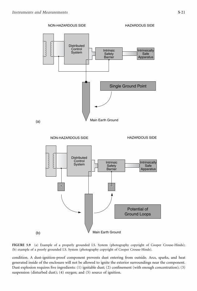
condition. A dust-ignition-proof component prevents dust entering from outside. Arcs, sparks, and heat
generated inside of the enclosure will not be allowed to ignite the exterior surroundings near the component.
Dust explosion requires five ingredients: (1) ignitable dust; (2) confinement (with enough concentration); (3)
suspension (disturbed dust); (4) oxygen; and (5) source of ignition.
DistributedControlSystem
IntrinsicSafetyBarrier
IntrinsicallySafe
Apparatus
NON-HAZARDOUS SIDE HAZARDOUS SIDE
Potential ofGround Loops
Main Earth Ground
Main Earth Ground
DistributedControlSystem
IntrinsicSafetyBarrier
IntrinsicallySafe
Apparatus
NON-HAZARDOUS SIDE HAZARDOUS SIDE
Single Ground Point
(a)
(b)
FIGURE 5.9 (a) Example of a properly grounded I.S. System (photography copyright of Cooper Crouse-Hinds);
(b) example of a poorly grounded I.S. System (photography copyright of Cooper Crouse-Hinds).
5-21Instruments and Measurements
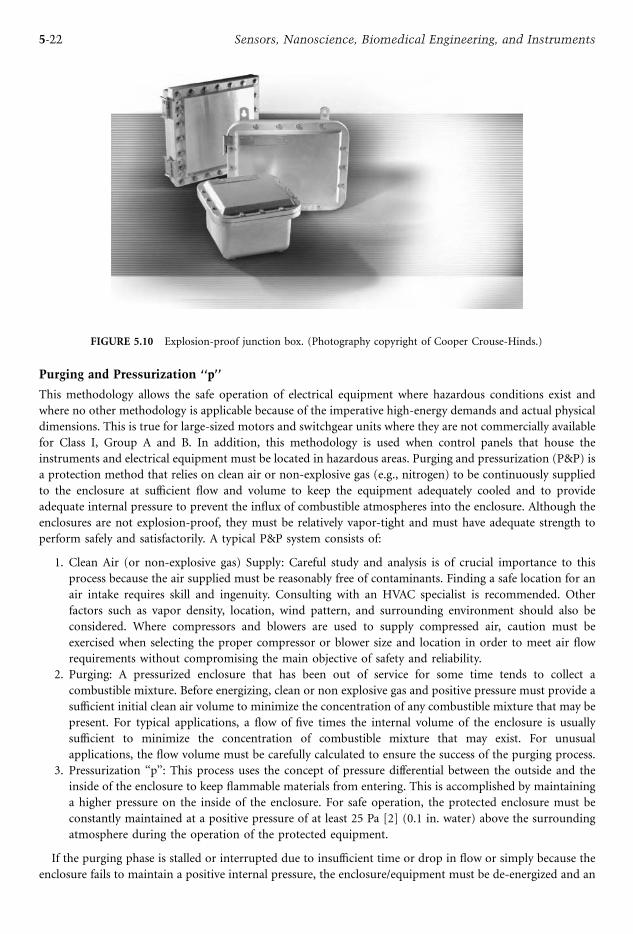
Purging and Pressurization ‘‘p’’
This methodology allows the safe operation of electrical equipment where hazardous conditions exist and
where no other methodology is applicable because of the imperative high-energy demands and actual physical
dimensions. This is true for large-sized motors and switchgear units where they are not commercially available
for Class I, Group A and B. In addition, this methodology is used when control panels that house the
instruments and electrical equipment must be located in hazardous areas. Purging and pressurization (P&P) is
a protection method that relies on clean air or non-explosive gas (e.g., nitrogen) to be continuously supplied
to the enclosure at sufficient flow and volume to keep the equipment adequately cooled and to provide
adequate internal pressure to prevent the influx of combustible atmospheres into the enclosure. Although the
enclosures are not explosion-proof, they must be relatively vapor-tight and must have adequate strength to
perform safely and satisfactorily. A typical P&P system consists of:
1. Clean Air (or non-explosive gas) Supply: Careful study and analysis is of crucial importance to this
process because the air supplied must be reasonably free of contaminants. Finding a safe location for an
air intake requires skill and ingenuity. Consulting with an HVAC specialist is recommended. Other
factors such as vapor density, location, wind pattern, and surrounding environment should also be
considered. Where compressors and blowers are used to supply compressed air, caution must be
exercised when selecting the proper compressor or blower size and location in order to meet air flow
requirements without compromising the main objective of safety and reliability.
2. Purging: A pressurized enclosure that has been out of service for some time tends to collect a
combustible mixture. Before energizing, clean or non explosive gas and positive pressure must provide a
sufficient initial clean air volume to minimize the concentration of any combustible mixture that may be
present. For typical applications, a flow of five times the internal volume of the enclosure is usually
sufficient to minimize the concentration of combustible mixture that may exist. For unusual
applications, the flow volume must be carefully calculated to ensure the success of the purging process.
3. Pressurization ‘‘p’’: This process uses the concept of pressure differential between the outside and the
inside of the enclosure to keep flammable materials from entering. This is accomplished by maintaining
a higher pressure on the inside of the enclosure. For safe operation, the protected enclosure must be
constantly maintained at a positive pressure of at least 25 Pa [2] (0.1 in. water) above the surrounding
atmosphere during the operation of the protected equipment.
If the purging phase is stalled or interrupted due to insufficient time or drop in flow or simply because the
enclosure fails to maintain a positive internal pressure, the enclosure/equipment must be de-energized and an
FIGURE 5.10 Explosion-proof junction box. (Photography copyright of Cooper Crouse-Hinds.)
5-22 Sensors, Nanoscience, Biomedical Engineering, and Instruments
alarm indication is initiated for Zone 1and Zone 2 respectively. If either purging or pressurization fail to
complete its cycle, the purging cycle starts be restarted and the two passed must be fully completed before
power is applied. The P&P process is normally controlled by a Purge Control Unit (PCU) which is required to
measure flow (air volume- purging) and pressure (internal/external), and time. Just like any other piece of
equipment to be used in hazardous areas, the operation of the PCU must also be assessed under abnormal
operating conditions such as fault conditions, relay failure, etc., since improper operation of the PCU can have
enormous safety impact. As a minimum, the enclosure that encapsulates the apparatus must conform to IP 40
protection (protection against solid foreign bodies >1 mm in diameter). The enclosure must have sufficient
mechanical integrity to withstand impacts, overpressures while at the same time allow for ease of flow of air.
The enclosure must prevent the communication of flames, sparks to the explosive surrounding outside the
enclosure. One way to do that is by installing a spark arrestor on the air outlets, or by venting the air to a non-
hazardous area free of explosive mixtures. There are two types of pressurization, namely:
1. Static Pressurization (SP): Also known as constant flow. Air supplied and pressurized continuously
from a non-hazardous area to avoid the influx of flammable gases/vapor inside the protected enclosure.
After a pre-set time, power is applied to the enclosure.
2. Dynamic Pressurization (DP): Also known as leakage compensation. A process that depends on
maintaining pressure in a protected enclosure or area. Normally after purging the protective gas is
passed continuously through the enclosure at a pressure just above that of the specified minimum to
maintain positive pressure.
3. Signals and Alarms: When positive pressure is lost, warnings and alarms are essential. Three types of
pressurization and alarms can be used, depending on the nature of the enclosure’s controls and the
degree of hazard outside. In addition, door interlocks are required to prevent opening of the protected
enclosure while the circuit is energized.
According to NFPA 496, there are three types of pressurization. They are:
Type X — reduces the classification within the protected enclosure from Division 1 to non-classified. This
usually involves a source of ignition housed in a tight enclosure located in a potentially hazardous
atmosphere. Type X requires a disconnecting means (flow or pressure switch) to completely and
automatically de-energize power to the protected enclosure immediately upon failure of the protective gas
supply (loss of either pressure or flow). The disconnecting means must be explosion-proof or intrinsically
safe, as it is usually located in the hazardous area.
Type Y — reduces the classification within the protected enclosure from Division 1 to Division 2. The
protected enclosure houses equipment rated for Division 2 and does not provide a source of ignition.
Therefore, no immediate hazard is created. Type Y requires a visual or audible alarm in case of system
failure. Caution: Safeguards must be established to ensure that any malfunction in the system does not raise
the external surface temperature of the enclosure to over 80% of the ignition temperature of the
combustible mixture present.
Type Z — reduces the classification within the protected enclosure from Division 2 to non-classified. Type
Z requires a visual or audible alarm to be activated if failure to maintain positive pressure or flow within the
protected enclosure has been detected.
More information regarding the Ex-p requirements can be found in IEC60079–2
Powder Filled ‘‘q’’
The filling medium used for this application can include quartz sand (the origin of the ‘‘q’’), glass beads, or
powder. This method of protection is used primarily for small electrical components that have no moving
parts (e.g., capacitor). The methodology uses a sealed enclosure (normally with a vent) containing any of the
filling mediums to cover the enclosed electrical components capable of producing a spark. This ensures that
under normal use no arc can be created that is able to ignite the explosive mixture inside the enclosure and the
surrounding hazardous area. The enclosure construction requirements are specific and can be one of two
types: 1) pressure test of 0.5 bar over-pressure for one minute and, if not protected by another enclosure,
5-23Instruments and Measurements

a minimum Ingress Protection of IP 54, the same requirement for Ex-e enclosures; 2) if the component is
protected by another enclosure, no specific requirements for the type of IP protection is required. It is
absolutely essential that the enclosure filled with the ‘‘q’’ medium. The maximum distance from live parts of
electrical components to earth fitted inside the metal enclosure or metal screen can vary from 10 to 50 mm,
depending on the voltage applied. If the enclosure is permanently factory sealed and the voltage does not
exceed 500 volts, the minimum distance between live parts or live parts to earth can be reduced by 5 mm. If
there are ‘‘flying leads’’ from the apparatus, they must be connected to Ex-e certified terminals. Ex ‘‘q’’ is used
in Europe for heavy equipment and is not used in instrumentation applications. More information regarding
the Ex ‘‘q’’ requirements can be found in IEC60079–5.
Oil Immersion ‘‘o’’
The Oil Immersion concept has been predominantly reserved for heavy-duty, high voltage switchgear. As the
name implies (oil immersion) the electrical parts are immersed in mineral (nonflammable or explosive) oil,
which will prevent any exposure of the arcing or sparking to an explosive atmosphere that may be present
above the surface of the oil. Furthermore the oil is designed and used to quench arcs and limit the temperature
rise on electrical parts. To ensure compliance with the oil immersion protection requirements, two issues must
be addressed: 1) All parts capable of producing arcs or sparks must be immersed in the oil no less than 25 mm
in depth; and 2) An acceptable and reliable method to check the oil level must be provided. Depending on the
type of mineral oil used, caution must be exercised, as some mineral oils are capable of producing explosive
gases (e.g., acetylene and hydrogen) gas when arcing occurs and consequently create a hazardous condition
that this methodology was intended to reduce. More information regarding the Ex-o requirements can be
found in IEC60079–6.
Non Sparking (Nonincendive) ‘‘n’’
This methodology is straight forward type of protection. Type ‘‘n’’ apparatus is standard equipment which,
under normal operation will not produce arcs, sparks, or generate surface temperatures high enough to cause
ignition and a fault capable of causing ignition is not likely to occur. Examples of normally arcing equipment
are relays, circuit breakers, adjustable resistors, switches, and motor brushes.
Nonincendive circuit
A circuit in which any arc or thermal effect produced under intended operating conditions of the equipment is
not capable, under the test conditions specified, of igniting the specified flammable gas- or vapor- air mixture.
Nonincendive component:
A component having contacts for making or breaking an incendive circuit and the contacting mechanism shall
be constructed so that the component is incapable of igniting the specified flammable gas- or vapor-air
mixture. The housing of a nonincendive component is not intended contain an explosion or to exclude the
flammable atmosphere..
This methodology does not have power level restrictions and is primarily used in Zone 2 hazardous areas.
More information regarding the Ex-n requirements can be found in IEC60079–15.
Encapsulation ‘‘m’’
Encapsulation is finding increased usage for printed circuit boards that are assembled in small rail mounted
housings similar to terminals. The Encapsulation concept is a type of protection in which sparking or heating
parts are enclosed in a compound in such a way that the explosive atmosphere cannot be ignited under
operating or installation conditions. The encapsulating compound is thermosetting, thermoplastic, epoxy,
resin (cold curing), or elastomeric material with or without fillers and/or additives, in their solid state. The
temperature range must satisfy the requirements of an appropriate standard for this type of protection.
(Thermal stability at maximum operating temperature.) The following must be considered:
1. Isc of a component during abnormal conditions (fault).
2. Controlled and limited temperature rise of the wiring and components.
5-24 Sensors, Nanoscience, Biomedical Engineering, and Instruments

3. Resistors, capacitors, diodes etc., must operate at no more than 66% of their rated voltage.
4. Air pockets and gaps must be avoided.
More information regarding the encapsulating compound for this type of protection can be found in
IEC60079–18
Increased Safety ‘‘e’’
As the name may imply, the increased safety concept relies on added measures and precautions to be taken to
prevent the source of ignition (spark, heat, etc.,) from accruing either internally or externally to the apparatus
under normal operating conditions. Therefore, devices such as switches and contactors are not allowed to be
used since arching and sparking is part of the operation of the device under normal cooperating conditions.
Increased Safety is most suited for non-sparking devices such as transformers and terminal boxes and is
primarily used in Zone 1 area. The enclosures housing devices that incorporate the Increased Safety
methodology must confirm to certain guidelines. The apparatus has an ingress protection (IP) rating, which is
similar to NEMA enclosure ratings such as NEMA 4. As a minimum the following must be met:
1. IP 54 (dust and water splash) for enclosures containing live parts
2. IP 44 (solid foreign bodies >1 mm in diameter and water splash)
3. Thermal tolerance
4. Resistance to chemicals (solvents)
5. Mechanical integrity/strength
Where terminals are used inside these enclosures, they must also confirm to certain guidelines such as:
1. Means to prevent the conductors from coming loose
2. Sufficient contact pressure
3. Temperature limitations
4. Maximum voltage rating
5. Terminals de-rating for both current and the conductors
Hermetically Sealed
The equipment is protected against the external atmosphere to prevent the entry of hazardous gases or vapors.
The seal is made by fusion, such as soldering, brazing, welding, or the fusion of glass to metal. A typical sealed
device that is constructed so that it cannot be opened, has no external operating mechanisms, and is sealed to
restrict entry of an external atmosphere without relying on gaskets. The device may contain arcing parts or
internal hot surfaces. Figure 5.11 shows a valve positioner with hermetically sealed feed switches. For
additional information refer to UL1604
Combustible Gas Detection System
Depending on the industrial facility, hundreds of industrial gases are usually present and used in different
manufacturing processing. Examples of some of these gases include Acetylene C2H2 - is a group A gas (2.8% LFL
and 31.0 UFL) that is lighter than air (0.9 vapor density), odorless, and colorless in its pure state. It can be a
health hazard since it is considered a simple asphyxiant. Acetylene can decompose spontaneously if pressure
exceeds 15 PSIG. Acetylene is the simplest member of unsaturated hydrocarbons known as alkynes or
acetylenes. Because of its LFL and wide flammability range, it is considered one of the most easily ignitible gases.
Another commonly used gas in commercial applications and the oldest refrigerant known and still used
today is Ammonia — NH3 — a group D gas (15% LFL and 28% UFL). Ammonia is lighter than air (0.6
vapor density), colorless, with a sharp odor, reactive, and corrosive. Anything more than a sniff and ammonia
can be fatal. Ammonia is a toxic product that is highly irritating to the mucous membranes and eyes. Contact
with the skin causes severe burns. Normally ammonia is shipped as a liquified gas (LG) under its own vapor
pressure of 114 PSIG. Its most extensive use is in soil fertilization. This application is used in the form of salts,
nitrates, and urea. Ammonia has many important uses including bulk chemicals, plastic, and explosive
5-25Instruments and Measurements
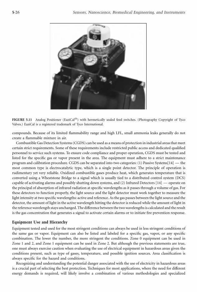
compounds. Because of its limited flammability range and high LFL, small ammonia leaks generally do not
create a flammable mixture in air.
Combustible GasDetection Systems (CGDS) can be used as ameans of protection in industrial areas thatmeet
certain strict requirements. Some of these requirements include restricted public access and dedicated qualified
personnel to service such systems. To ensure code compliance and proper operation, CGDS must be tested and
listed for the specific gas or vapor present in the area. The equipment must adhere to a strict maintenance
program and calibration procedure. CGDS can be separated into two categories: (1) Passive Systems[14] — the
most common type is electrocatalytic type, which is a single point detector. The principle of operation is
rudimentary yet very reliable. Oxidized combustible gases produce heat, which generates temperature that is
converted using a Wheatstone Bridge to a signal which is usually tied to a distributed control system (DCS)
capable of activating alarms and possibly shutting down systems, and (2) Infrared Detectors [14] — operate on
the principal of absorption of infrared radiation at specific wavelengths as it passes through a volume of gas. For
these detectors to function properly, the light source and the light detector must work together to measure the
light intensity at two specific wavelengths: active and reference. As the gas passes between the light source and the
detector, the amount of light in the active wavelength hitting the detector is reduced while the amount of light in
the referencewavelength stays unchanged. The difference between the twowavelengths is calculated and the result
is the gas concentration that generates a signal to activate certain alarms or to initiate fire prevention response.
Equipment Use and Hierarchy
Equipment tested and used for the most stringent conditions can always be used in less stringent conditions of
the same gas or vapor. Equipment can also be listed and labeled for a specific gas, vapor, or any specific
combination. The lower the number, the more stringent the conditions. Zone 0 equipment can be used in
Zone 1 and 2, and Zone 1 equipment can be used in Zone 2. But although the previous statements are true,
one must always exercise caution when evaluating the use of electrical equipment in hazardous areas given the
conditions present, such as type of gases, temperature, and possible ignition sources. Area classification is
always specific for the hazard and conditions.
Recognizing and understanding the potential danger associated with the use of electricity in hazardous areas
is a crucial part of selecting the best protection. Techniques for most applications, where the need for different
energy demands is required, will likely involve a combination of various methodologies and specialized
FIGURE 5.11 Analog Positioner (EaziCal2) with hermetically sealed feed switches. (Photography Copyright of Tyco
Valves.) EaziCal is a registered trademark of Tyco International.
5-26 Sensors, Nanoscience, Biomedical Engineering, and Instruments

technologies. Properly performed analysis and investigation may appear to be time-consuming and expensive,
but for those who are willing to adhere to the established guidelines and solid engineering practices, the
process will help ensure the highest level of compliance while yielding tremendous savings and preventing
property damage and injuries.
Defining Terms
Inductance: The ability of an electrical apparatus to store an electrical charge (energy). An inductor will
release this energy when the circuit is opened (broken).
Oxidation: The process where negatively charged ions (anions) lose electrons at the anode during electro-
chemical process. For anions to become neutral, they must lose electrons.
RTD: A device that measures temperature based on change of resistance.
Ground: A conducting connection, whether intentional or accidental, between an electrical circuit or
equipment and the earth or to some conducting body that serves in place of the earth.
Zener diode: A nonlinear solid state device that does not conduct current in reverse bias mode until a
critical voltage is reached. It is then able to conduct current in reverse bias without damage to the diode.
Zener diodes have almost constant voltage characteristics in the reverse-bias region (usual operation).
Normal Operation: Refers to the equipment and installation operation within their design parameters.
References
1. NFPA 70 (ANCI C1 - 2004), National Electrical Code 2004, Quincy.
2. National Fire Protection Association (NFPA), Articles 493, 496, 497, Quincy.
3. American Petroleum Institute 500 (RP 500), 1st ed., Washington, DC, June 1991. Recommended Practice
For Classification of Location For Electrical Installation at Petroleum Facilities.
4. Elcon Instruments, Inc., Introduction To Intrinsic Safety, 3rd print, Norcross, 1990.
5. Underwriters Laboratories, Inc., Pub. UL 913, 4th ed., Northbrook, 1988, Standard for Intrinsically Safe
Apparatus & Associated Apparatus For Use In Class I, II, III, Division 1 Hazardous Locations.
6. Underwriters Laboratories, Inc., Pub. UL 508, Industrial Control Equipment.
7. Babiarz, P., Cooper Industries, Crouse-Hinds, InTech Engineer’s Notebook, Syracuse, 1994.
8. R. Stahl, Inc., RST 49, Comprehensive Applications and Data Catalog, Woburn, 1992.
9. Oudar, J., Intrinsic Safety, Journal of the Southern California Meter Association, October, 1981.
10. Alexander, W., Intrinsically Safe Systems, InTech, April 1996.
11. Tyco Thermal Controls, H56895, August 2003
12. Sean Clarke, Epsilon Technical Services Limited
13. Copper Crouse-Hinds 2004 EX Digest
14. General Monitors, Fundamentals of Combustible Gas Detection
5.2 Portable Instruments and Systems
Halit Eren
Introduction
Measurement, a process of gathering information from the physical world, is carried out by using measuring
instruments. Instruments are man-made devices that are designed to maintain prescribed relationships between
the parameters being sensed and the physical variable under investigation. Modern measuring instruments can
be categorized in a number of ways based on operational principles, application areas, and physical charac-
teristics of the instruments. Physical characteristics differentiate measuring instruments into two broad groups:
. Portable instruments with self-powering capabilities
. Non-portable or fixed instruments that require external power
5-27Instruments and Measurements
Further, portable instruments can be divided into three main groups:
. Portable and hand-held instruments that are built for specific applications
. Intelligent-sensors in a single chip that function as a complete instrument
. Portable data systems that contain portable or fixed devices and are capable of communicating with
other digital systems
All three forms of portable instruments are used in a variety of applications, including: science and
engineering, laboratories, medicine, environmental monitoring systems, chemical processes, biology, oil and gas
industry, aerospace, manufacturing, military, navigation, personal security, and hobby devices. In recent years,
many devices conventionally known as bench-top instruments are being replaced by their portable counterparts
thanks to improvements in supporting technologies. As the electronic components for all instruments get smaller
in the form of microelectronics, and the software support becomes widely available, the physical dimensions of
conventional instruments become smaller day by day. As a result, the trend of miniaturization of larger and
bulkier instruments opens up many new avenues for development and applications of portable instruments.
In previous years, due to the unique nature of instrumentation hardware, customized software support was
necessary from instrument to instrument. Nevertheless, today’s portable instruments are largely software-
driven and can be programmed by commonly available software tools. Therefore, many standards such as the
IEEE-1451 can now be implemented in portable devices; hence the front-end and back-end analog and digital
hardware of portable instruments can now be standardized to address large classes of similar applications.
In this section, a general concept for portable instruments will be introduced and recent progress in this area
will be discussed. Further information can be found in the publications listed in the Reference section.
Features of Portable Instruments
Portable instruments have special features that are decided and shaped in the early stages of design and
construction. Compared to non-portables, portable instruments are centered on the trade-offs between
instrument cost, performance, small size, less weight, low power consumption, user-friendly interface options,
ruggedness, and ability to operate in a diverse range of environments. Due to their portability, these devices
must be able to withstand accidental or deliberate abuses such as drops and knocks, be able to operate under
harsh conditions in extreme heat and cold, even in rain and water. Often they may be handled by untrained
users. Consequently, portable instruments require finely tuned features that balance performance against
power consumption, weight against ruggedness, and simple user interface needs against convenience of
operations, at the same time maintaining reasonable cost.
Portable instruments have the following general features that differentiate them from nonportables:
. Available power is limited.
. Voltage level to supply the electronic components will generally be low, usually less than 12 V.
. Under normal operating conditions, power supply voltage levels may vary considerably due to
diminishing stored power. Even if the portable instruments are kept on shelves without being used the
power of batteries may diminish due to leakage.. Conditions of use and environments in which portable instruments operate may vary often. The
possibility of portable instruments being subjected to severe variations in temperature moisture, and
intense electromagnetic noise increases.. Likelihood of the portable instruments being operated by unskilled and untrained users is greater.. The human-machine interface of electronic portable instruments may be very different from that of
nonportable counterparts.. Weight and size may be dominant factors.
Important features of portable instruments are discussed in the following subsections.
Power Requirements of Portable Instruments
Power available in portable instruments is limited. Therefore, the restriction of power consumption is perhaps
the most significant problem in their design and application. As a rule, better performance demands more
5-28 Sensors, Nanoscience, Biomedical Engineering, and Instruments
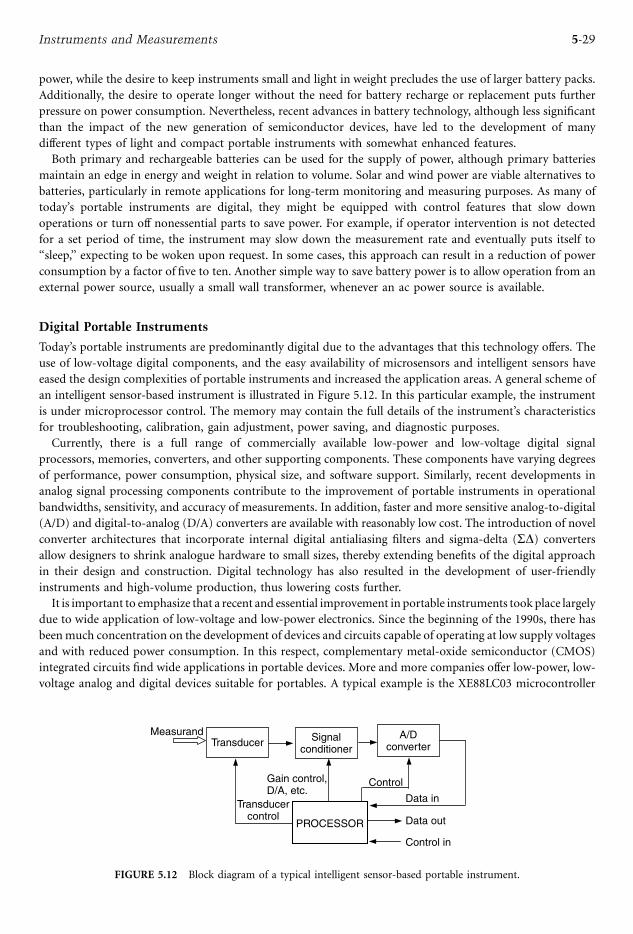
power, while the desire to keep instruments small and light in weight precludes the use of larger battery packs.
Additionally, the desire to operate longer without the need for battery recharge or replacement puts further
pressure on power consumption. Nevertheless, recent advances in battery technology, although less significant
than the impact of the new generation of semiconductor devices, have led to the development of many
different types of light and compact portable instruments with somewhat enhanced features.
Both primary and rechargeable batteries can be used for the supply of power, although primary batteries
maintain an edge in energy and weight in relation to volume. Solar and wind power are viable alternatives to
batteries, particularly in remote applications for long-term monitoring and measuring purposes. As many of
today’s portable instruments are digital, they might be equipped with control features that slow down
operations or turn off nonessential parts to save power. For example, if operator intervention is not detected
for a set period of time, the instrument may slow down the measurement rate and eventually puts itself to
‘‘sleep,’’ expecting to be woken upon request. In some cases, this approach can result in a reduction of power
consumption by a factor of five to ten. Another simple way to save battery power is to allow operation from an
external power source, usually a small wall transformer, whenever an ac power source is available.
Digital Portable Instruments
Today’s portable instruments are predominantly digital due to the advantages that this technology offers. The
use of low-voltage digital components, and the easy availability of microsensors and intelligent sensors have
eased the design complexities of portable instruments and increased the application areas. A general scheme of
an intelligent sensor-based instrument is illustrated in Figure 5.12. In this particular example, the instrument
is under microprocessor control. The memory may contain the full details of the instrument’s characteristics
for troubleshooting, calibration, gain adjustment, power saving, and diagnostic purposes.
Currently, there is a full range of commercially available low-power and low-voltage digital signal
processors, memories, converters, and other supporting components. These components have varying degrees
of performance, power consumption, physical size, and software support. Similarly, recent developments in
analog signal processing components contribute to the improvement of portable instruments in operational
bandwidths, sensitivity, and accuracy of measurements. In addition, faster and more sensitive analog-to-digital
(A/D) and digital-to-analog (D/A) converters are available with reasonably low cost. The introduction of novel
converter architectures that incorporate internal digital antialiasing filters and sigma-delta (SD) convertersallow designers to shrink analogue hardware to small sizes, thereby extending benefits of the digital approach
in their design and construction. Digital technology has also resulted in the development of user-friendly
instruments and high-volume production, thus lowering costs further.
It is important to emphasize that a recent and essential improvement in portable instruments took place largely
due to wide application of low-voltage and low-power electronics. Since the beginning of the 1990s, there has
beenmuch concentration on the development of devices and circuits capable of operating at low supply voltages
and with reduced power consumption. In this respect, complementary metal-oxide semiconductor (CMOS)
integrated circuits find wide applications in portable devices. More and more companies offer low-power, low-
voltage analog and digital devices suitable for portables. A typical example is the XE88LC03 microcontroller
Transducer Signalconditioner
A/Dconverter
Data in
PROCESSOR Data out
Control in
Transducercontrol
Gain control,D/A, etc.
Control
Measurand
FIGURE 5.12 Block diagram of a typical intelligent sensor-based portable instrument.
5-29Instruments and Measurements
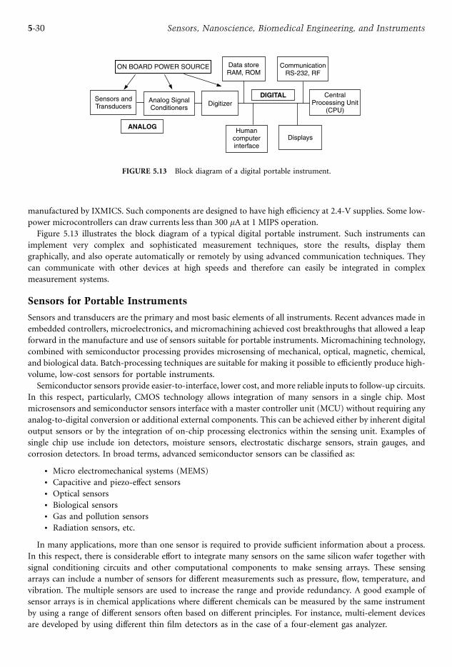
manufactured by IXMICS. Such components are designed to have high efficiency at 2.4-V supplies. Some low-
power microcontrollers can draw currents less than 300 mA at 1 MIPS operation.Figure 5.13 illustrates the block diagram of a typical digital portable instrument. Such instruments can
implement very complex and sophisticated measurement techniques, store the results, display them
graphically, and also operate automatically or remotely by using advanced communication techniques. They
can communicate with other devices at high speeds and therefore can easily be integrated in complex
measurement systems.
Sensors for Portable Instruments
Sensors and transducers are the primary and most basic elements of all instruments. Recent advances made in
embedded controllers, microelectronics, and micromachining achieved cost breakthroughs that allowed a leap
forward in the manufacture and use of sensors suitable for portable instruments. Micromachining technology,
combined with semiconductor processing provides microsensing of mechanical, optical, magnetic, chemical,
and biological data. Batch-processing techniques are suitable for making it possible to efficiently produce high-
volume, low-cost sensors for portable instruments.
Semiconductor sensors provide easier-to-interface, lower cost, and more reliable inputs to follow-up circuits.
In this respect, particularly, CMOS technology allows integration of many sensors in a single chip. Most
microsensors and semiconductor sensors interface with a master controller unit (MCU) without requiring any
analog-to-digital conversion or additional external components. This can be achieved either by inherent digital
output sensors or by the integration of on-chip processing electronics within the sensing unit. Examples of
single chip use include ion detectors, moisture sensors, electrostatic discharge sensors, strain gauges, and
corrosion detectors. In broad terms, advanced semiconductor sensors can be classified as:
. Micro electromechanical systems (MEMS)
. Capacitive and piezo-effect sensors
. Optical sensors
. Biological sensors
. Gas and pollution sensors
. Radiation sensors, etc.
In many applications, more than one sensor is required to provide sufficient information about a process.
In this respect, there is considerable effort to integrate many sensors on the same silicon wafer together with
signal conditioning circuits and other computational components to make sensing arrays. These sensing
arrays can include a number of sensors for different measurements such as pressure, flow, temperature, and
vibration. The multiple sensors are used to increase the range and provide redundancy. A good example of
sensor arrays is in chemical applications where different chemicals can be measured by the same instrument
by using a range of different sensors often based on different principles. For instance, multi-element devices
are developed by using different thin film detectors as in the case of a four-element gas analyzer.
Sensors andTransducers
Analog SignalConditioners
DigitizerCentral
Processing Unit(CPU)
Data storeRAM, ROM
CommunicationRS-232, RF
DisplaysHuman
computerinterface
ON BOARD POWER SOURCE
DIGITAL
ANALOG
FIGURE 5.13 Block diagram of a digital portable instrument.
5-30 Sensors, Nanoscience, Biomedical Engineering, and Instruments
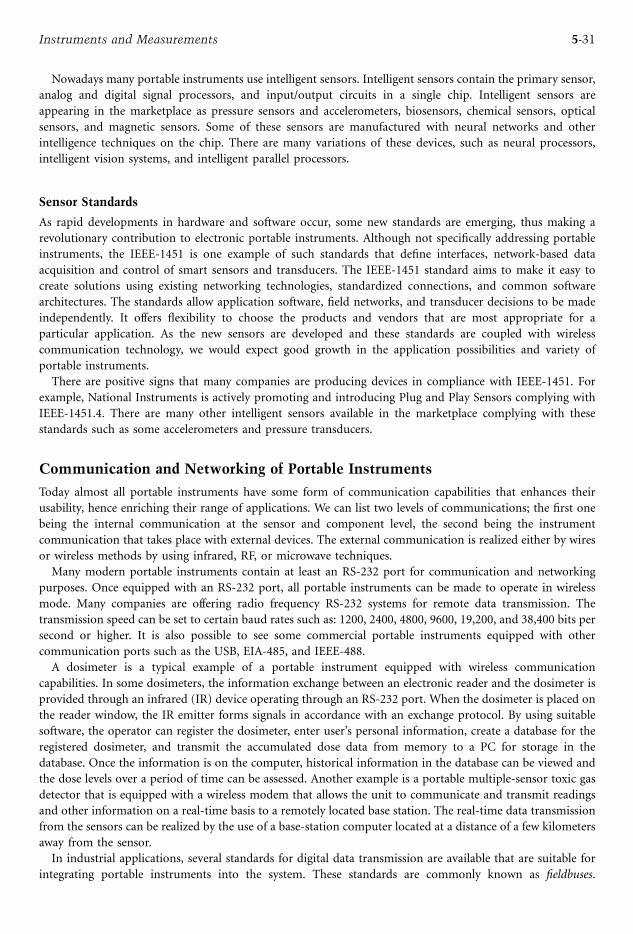
Nowadays many portable instruments use intelligent sensors. Intelligent sensors contain the primary sensor,
analog and digital signal processors, and input/output circuits in a single chip. Intelligent sensors are
appearing in the marketplace as pressure sensors and accelerometers, biosensors, chemical sensors, optical
sensors, and magnetic sensors. Some of these sensors are manufactured with neural networks and other
intelligence techniques on the chip. There are many variations of these devices, such as neural processors,
intelligent vision systems, and intelligent parallel processors.
Sensor Standards
As rapid developments in hardware and software occur, some new standards are emerging, thus making a
revolutionary contribution to electronic portable instruments. Although not specifically addressing portable
instruments, the IEEE-1451 is one example of such standards that define interfaces, network-based data
acquisition and control of smart sensors and transducers. The IEEE-1451 standard aims to make it easy to
create solutions using existing networking technologies, standardized connections, and common software
architectures. The standards allow application software, field networks, and transducer decisions to be made
independently. It offers flexibility to choose the products and vendors that are most appropriate for a
particular application. As the new sensors are developed and these standards are coupled with wireless
communication technology, we would expect good growth in the application possibilities and variety of
portable instruments.
There are positive signs that many companies are producing devices in compliance with IEEE-1451. For
example, National Instruments is actively promoting and introducing Plug and Play Sensors complying with
IEEE-1451.4. There are many other intelligent sensors available in the marketplace complying with these
standards such as some accelerometers and pressure transducers.
Communication and Networking of Portable Instruments
Today almost all portable instruments have some form of communication capabilities that enhances their
usability, hence enriching their range of applications. We can list two levels of communications; the first one
being the internal communication at the sensor and component level, the second being the instrument
communication that takes place with external devices. The external communication is realized either by wires
or wireless methods by using infrared, RF, or microwave techniques.
Many modern portable instruments contain at least an RS-232 port for communication and networking
purposes. Once equipped with an RS-232 port, all portable instruments can be made to operate in wireless
mode. Many companies are offering radio frequency RS-232 systems for remote data transmission. The
transmission speed can be set to certain baud rates such as: 1200, 2400, 4800, 9600, 19,200, and 38,400 bits per
second or higher. It is also possible to see some commercial portable instruments equipped with other
communication ports such as the USB, EIA-485, and IEEE-488.
A dosimeter is a typical example of a portable instrument equipped with wireless communication
capabilities. In some dosimeters, the information exchange between an electronic reader and the dosimeter is
provided through an infrared (IR) device operating through an RS-232 port. When the dosimeter is placed on
the reader window, the IR emitter forms signals in accordance with an exchange protocol. By using suitable
software, the operator can register the dosimeter, enter user’s personal information, create a database for the
registered dosimeter, and transmit the accumulated dose data from memory to a PC for storage in the
database. Once the information is on the computer, historical information in the database can be viewed and
the dose levels over a period of time can be assessed. Another example is a portable multiple-sensor toxic gas
detector that is equipped with a wireless modem that allows the unit to communicate and transmit readings
and other information on a real-time basis to a remotely located base station. The real-time data transmission
from the sensors can be realized by the use of a base-station computer located at a distance of a few kilometers
away from the sensor.
In industrial applications, several standards for digital data transmission are available that are suitable for
integrating portable instruments into the system. These standards are commonly known as fieldbuses.
5-31Instruments and Measurements
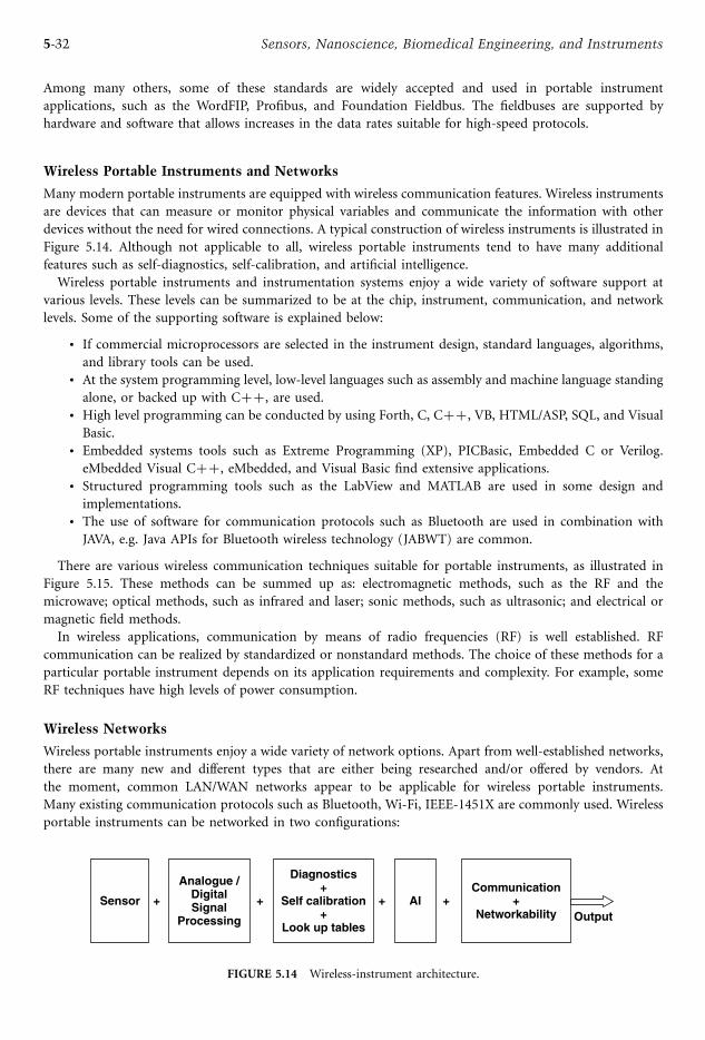
Among many others, some of these standards are widely accepted and used in portable instrument
applications, such as the WordFIP, Profibus, and Foundation Fieldbus. The fieldbuses are supported by
hardware and software that allows increases in the data rates suitable for high-speed protocols.
Wireless Portable Instruments and Networks
Many modern portable instruments are equipped with wireless communication features. Wireless instruments
are devices that can measure or monitor physical variables and communicate the information with other
devices without the need for wired connections. A typical construction of wireless instruments is illustrated in
Figure 5.14. Although not applicable to all, wireless portable instruments tend to have many additional
features such as self-diagnostics, self-calibration, and artificial intelligence.
Wireless portable instruments and instrumentation systems enjoy a wide variety of software support at
various levels. These levels can be summarized to be at the chip, instrument, communication, and network
levels. Some of the supporting software is explained below:
. If commercial microprocessors are selected in the instrument design, standard languages, algorithms,
and library tools can be used.. At the system programming level, low-level languages such as assembly and machine language standing
alone, or backed up with Cþþ, are used.. High level programming can be conducted by using Forth, C, Cþþ, VB, HTML/ASP, SQL, and VisualBasic.
. Embedded systems tools such as Extreme Programming (XP), PICBasic, Embedded C or Verilog.
eMbedded Visual Cþþ, eMbedded, and Visual Basic find extensive applications.. Structured programming tools such as the LabView and MATLAB are used in some design and
implementations.. The use of software for communication protocols such as Bluetooth are used in combination with
JAVA, e.g. Java APIs for Bluetooth wireless technology (JABWT) are common.
There are various wireless communication techniques suitable for portable instruments, as illustrated in
Figure 5.15. These methods can be summed up as: electromagnetic methods, such as the RF and the
microwave; optical methods, such as infrared and laser; sonic methods, such as ultrasonic; and electrical or
magnetic field methods.
In wireless applications, communication by means of radio frequencies (RF) is well established. RF
communication can be realized by standardized or nonstandard methods. The choice of these methods for a
particular portable instrument depends on its application requirements and complexity. For example, some
RF techniques have high levels of power consumption.
Wireless Networks
Wireless portable instruments enjoy a wide variety of network options. Apart from well-established networks,
there are many new and different types that are either being researched and/or offered by vendors. At
the moment, common LAN/WAN networks appear to be applicable for wireless portable instruments.
Many existing communication protocols such as Bluetooth, Wi-Fi, IEEE-1451X are commonly used. Wireless
portable instruments can be networked in two configurations:
Sensor +
Analogue /DigitalSignal
Processing
Communication+
Networkability+
Diagnostics+
Self calibration+
Look up tablesOutput
++ AI
FIGURE 5.14 Wireless-instrument architecture.
5-32 Sensors, Nanoscience, Biomedical Engineering, and Instruments
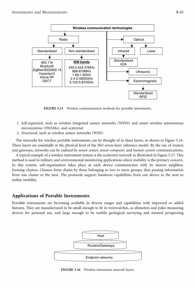
1. Self-organized, such as wireless integrated sensor networks (WINS) and smart wireless autonomous
microsystems (SWAMs), and scatternet
2. Structured, such as wireless sensor networks (WSN)
The networks for wireless portable instruments can be thought of in three layers, as shown in Figure 5.16.
These layers are essentially at the physical level of the ISO seven-layer reference model. By the use of routers
and gateways, networks can be realized by sensor-sensor, sensor-computer, and human-system communications.
A typical example of a wireless instrument system is the scatternet network as illustrated in Figure 5.17. This
method is used in military and environmental monitoring applications where mobility is the primary concern.
In this system, self-organization takes place as each device communicates with its nearest neighbor,
forming clusters. Clusters form chains by those belonging to two or more groups, thus passing information
from one cluster to the next. The protocols support handover capabilities from one device to the next to
realize mobility.
Applications of Portable Instruments
Portable instruments are becoming available in diverse ranges and capabilities with improved or added
features. They are manufactured to be small enough to fit in wristwatches, as altimeters and pulse measuring
devices for personal use, and large enough to be mobile geological surveying and mineral prospecting
Wireless communication technologies
Radio Optical
Ultrasonic
Electromagnetic
Non-standardizedStandardized
802.11bBluetooth
ZigBee/IEEE802.15Hyperlan/2Home RF
DECT
ISM bands
433.5-434.37MHz868-870MHz1.68-1.9GHz
2.4-2.4835GHz5.725-5.875GHz
Infrared Laser
StandardizedIrDA
StandardizedRFID
FIGURE 5.15 Wireless communication methods for portable instruments.
Endpoint networks
Routers/Gateways
Host
FIGURE 5.16 Wireless instrument network layers.
5-33Instruments and Measurements
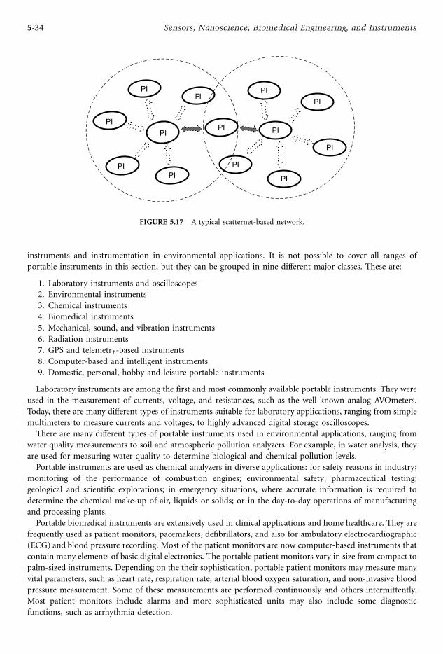
instruments and instrumentation in environmental applications. It is not possible to cover all ranges of
portable instruments in this section, but they can be grouped in nine different major classes. These are:
1. Laboratory instruments and oscilloscopes
2. Environmental instruments
3. Chemical instruments
4. Biomedical instruments
5. Mechanical, sound, and vibration instruments
6. Radiation instruments
7. GPS and telemetry-based instruments
8. Computer-based and intelligent instruments
9. Domestic, personal, hobby and leisure portable instruments
Laboratory instruments are among the first and most commonly available portable instruments. They were
used in the measurement of currents, voltage, and resistances, such as the well-known analog AVOmeters.
Today, there are many different types of instruments suitable for laboratory applications, ranging from simple
multimeters to measure currents and voltages, to highly advanced digital storage oscilloscopes.
There are many different types of portable instruments used in environmental applications, ranging from
water quality measurements to soil and atmospheric pollution analyzers. For example, in water analysis, they
are used for measuring water quality to determine biological and chemical pollution levels.
Portable instruments are used as chemical analyzers in diverse applications: for safety reasons in industry;
monitoring of the performance of combustion engines; environmental safety; pharmaceutical testing;
geological and scientific explorations; in emergency situations, where accurate information is required to
determine the chemical make-up of air, liquids or solids; or in the day-to-day operations of manufacturing
and processing plants.
Portable biomedical instruments are extensively used in clinical applications and home healthcare. They are
frequently used as patient monitors, pacemakers, defibrillators, and also for ambulatory electrocardiographic
(ECG) and blood pressure recording. Most of the patient monitors are now computer-based instruments that
contain many elements of basic digital electronics. The portable patient monitors vary in size from compact to
palm-sized instruments. Depending on the their sophistication, portable patient monitors may measure many
vital parameters, such as heart rate, respiration rate, arterial blood oxygen saturation, and non-invasive blood
pressure measurement. Some of these measurements are performed continuously and others intermittently.
Most patient monitors include alarms and more sophisticated units may also include some diagnostic
functions, such as arrhythmia detection.
PIPI
PI
PIPI
PIPI
PI
PI
PI
PI
PI
PI
FIGURE 5.17 A typical scatternet-based network.
5-34 Sensors, Nanoscience, Biomedical Engineering, and Instruments
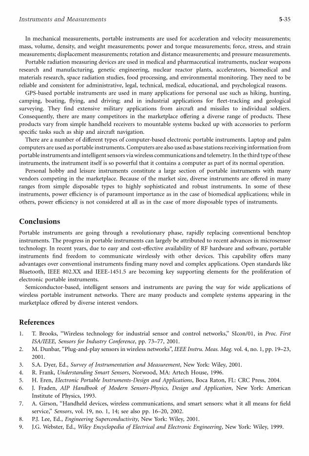
In mechanical measurements, portable instruments are used for acceleration and velocity measurements;
mass, volume, density, and weight measurements; power and torque measurements; force, stress, and strain
measurements; displacement measurements; rotation and distance measurements; and pressure measurements.
Portable radiation measuring devices are used in medical and pharmaceutical instruments, nuclear weapons
research and manufacturing, genetic engineering, nuclear reactor plants, accelerators, biomedical and
materials research, space radiation studies, food processing, and environmental monitoring. They need to be
reliable and consistent for administrative, legal, technical, medical, educational, and psychological reasons.
GPS-based portable instruments are used in many applications for personal use such as hiking, hunting,
camping, boating, flying, and driving; and in industrial applications for fleet-tracking and geological
surveying. They find extensive military applications from aircraft and missiles to individual soldiers.
Consequently, there are many competitors in the marketplace offering a diverse range of products. These
products vary from simple handheld receivers to mountable systems backed up with accessories to perform
specific tasks such as ship and aircraft navigation.
There are a number of different types of computer-based electronic portable instruments. Laptop and palm
computers are used as portable instruments. Computers are also used as base stations receiving information from
portable instruments and intelligent sensors viawireless communications and telemetry. In the third type of these
instruments, the instrument itself is so powerful that it contains a computer as part of its normal operation.
Personal hobby and leisure instruments constitute a large section of portable instruments with many
vendors competing in the marketplace. Because of the market size, diverse instruments are offered in many
ranges from simple disposable types to highly sophisticated and robust instruments. In some of these
instruments, power efficiency is of paramount importance as in the case of biomedical applications; while in
others, power efficiency is not considered at all as in the case of more disposable types of instruments.
Conclusions
Portable instruments are going through a revolutionary phase, rapidly replacing conventional benchtop
instruments. The progress in portable instruments can largely be attributed to recent advances in microsensor
technology. In recent years, due to easy and cost-effective availability of RF hardware and software, portable
instruments find freedom to communicate wirelessly with other devices. This capability offers many
advantages over conventional instruments finding many novel and complex applications. Open standards like
Bluetooth, IEEE 802.XX and IEEE-1451.5 are becoming key supporting elements for the proliferation of
electronic portable instruments.
Semiconductor-based, intelligent sensors and instruments are paving the way for wide applications of
wireless portable instrument networks. There are many products and complete systems appearing in the
marketplace offered by diverse interest vendors.
References
1. T. Brooks, ‘‘Wireless technology for industrial sensor and control networks,’’ SIcon/01, in Proc. First
ISA/IEEE, Sensors for Industry Conference, pp. 73–77, 2001.
2. M. Dunbar, ‘‘Plug-and-play sensors in wireless networks’’, IEEE Instru. Meas. Mag. vol. 4, no. 1, pp. 19–23,
2001.
3. S.A. Dyer, Ed., Survey of Instrumentation and Measurement, New York: Wiley, 2001.
4. R. Frank, Understanding Smart Sensors, Norwood, MA: Artech House, 1996.
5. H. Eren, Electronic Portable Instruments-Design and Applications, Boca Raton, FL: CRC Press, 2004.
6. J. Fraden, AIP Handbook of Modern Sensors-Physics, Design and Application, New York: American
Institute of Physics, 1993.
7. A. Girson, ‘‘Handheld devices, wireless communications, and smart sensors: what it all means for field
service,’’ Sensors, vol. 19, no. 1, 14; see also pp. 16–20, 2002.
8. P.J. Lee, Ed., Engineering Superconductivity, New York: Wiley, 2001.
9. J.G. Webster, Ed., Wiley Encyclopedia of Electrical and Electronic Engineering, New York: Wiley, 1999.
5-35Instruments and Measurements

5.3 G (LabVIEWTM) Software Engineering
Christopher G. Relf
The LabVIEW (Laboratory Virtual Instrument Engineering Workbench) development system has certainly
matured beyond its original role of simple laboratory bench experiment automation and data collection—it
has become a full-featured programming language (known as G) in its own right. Although National
Instruments (the creators of LabVIEW) continues to push its rapid prototyping and code development
virtues, an increasing number of G software developers are relying on advanced programming techniques, far
beyond those initially apparent.
The documentation that ships with a standard LabVIEW installation is sufficient to assist the development
of simple applications by users not initially familiar with LabVIEW, and the various online documents
provided by National Instruments and third-party vendors extend that learning experience. This chapter
attempts to describe some of the features, methods, and more obscure tidbits of programming expertise that
are of use to the advanced G software engineer.
Data Types
Like most modern programming languages, G code uses various data types. These data types allow for efficient
data storage, transmission, manipulation, and processing of information. Simple data types include the
integer, floating point, strings, paths, arrays, clusters, and reference numbers (refnums). The method G uses to
store data depends on its type, and it is important to understand the way data will reside in memory. Savvy use
of data types decreases the overall memory footprint of an application, minimizes data coercion errors, and
improves system performance.
Figure 5.18 lists representations of the standard numerical data types available to G. Others exist, including
the extended-precision float, although its representation is platform dependent, as shown in Figure 5.19. (The
representation of an extended-precision float is identical to a double-precision float when using HP-UX.)
Unlike numerical values, strings are represented by dimension-defined arrays (Figure 5.20). Each array
consists of a 4-byte integer that contains the number of characters required to represent the string, and
FIGURE 5.18 Numerical data types.
5-36 Sensors, Nanoscience, Biomedical Engineering, and Instruments
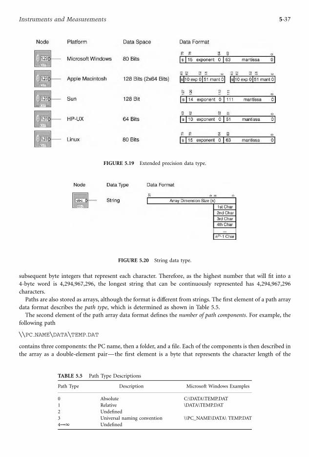
subsequent byte integers that represent each character. Therefore, as the highest number that will fit into a
4-byte word is 4,294,967,296, the longest string that can be continuously represented has 4,294,967,296
characters.
Paths are also stored as arrays, although the format is different from strings. The first element of a path array
data format describes the path type, which is determined as shown in Table 5.5.
The second element of the path array data format defines the number of path components. For example, the
following path
nnPC NAMEnDATAnTEMP:DATcontains three components: the PC name, then a folder, and a file. Each of the components is then described in
the array as a double-element pair—the first element is a byte that represents the character length of the
FIGURE 5.19 Extended precision data type.
TABLE 5.5 Path Type Descriptions
Path Type Description Microsoft Windows Examples
0 Absolute C:\DATA\TEMP.DAT
1 Relative \DATA\TEMP.DAT
2 Undefined
3 Universal naming convention \\PC_NAME\DATA\ TEMP.DAT
4!1 Undefined
FIGURE 5.20 String data type.
5-37Instruments and Measurements
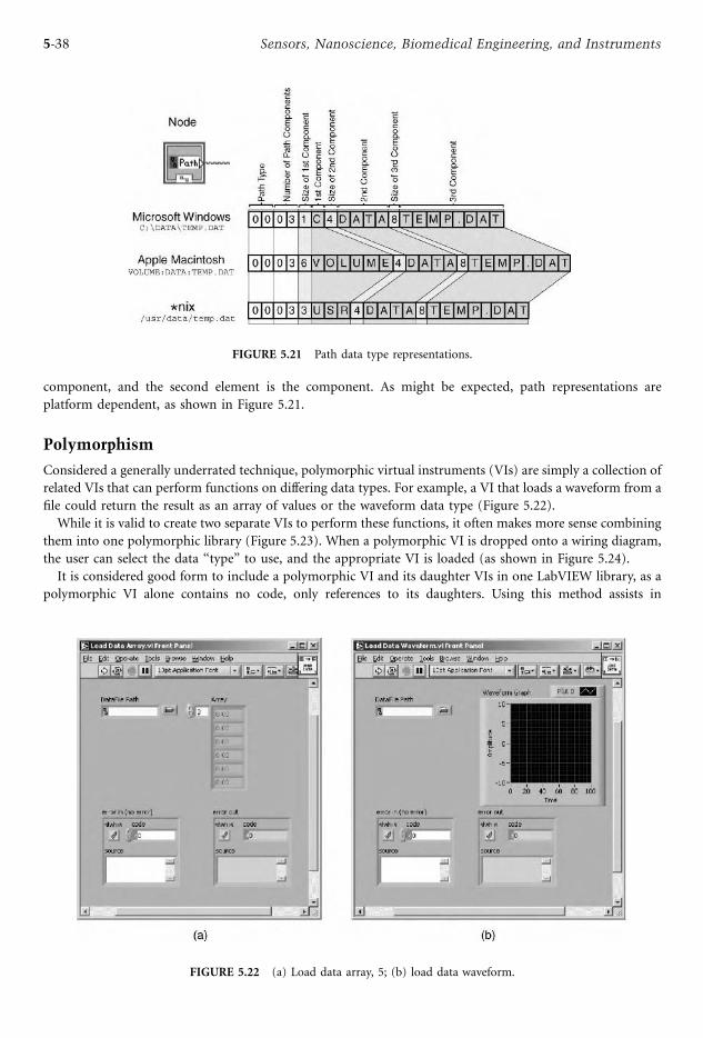
component, and the second element is the component. As might be expected, path representations are
platform dependent, as shown in Figure 5.21.
Polymorphism
Considered a generally underrated technique, polymorphic virtual instruments (VIs) are simply a collection of
related VIs that can perform functions on differing data types. For example, a VI that loads a waveform from a
file could return the result as an array of values or the waveform data type (Figure 5.22).
While it is valid to create two separate VIs to perform these functions, it often makes more sense combining
them into one polymorphic library (Figure 5.23). When a polymorphic VI is dropped onto a wiring diagram,
the user can select the data ‘‘type’’ to use, and the appropriate VI is loaded (as shown in Figure 5.24).
It is considered good form to include a polymorphic VI and its daughter VIs in one LabVIEW library, as a
polymorphic VI alone contains no code, only references to its daughters. Using this method assists in
FIGURE 5.21 Path data type representations.
FIGURE 5.22 (a) Load data array, 5; (b) load data waveform.
5-38 Sensors, Nanoscience, Biomedical Engineering, and Instruments
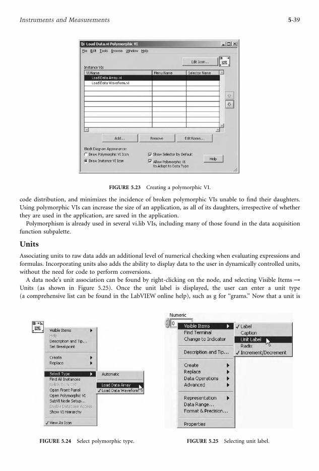
code distribution, and minimizes the incidence of broken polymorphic VIs unable to find their daughters.
Using polymorphic VIs can increase the size of an application, as all of its daughters, irrespective of whether
they are used in the application, are saved in the application.
Polymorphism is already used in several vi.lib VIs, including many of those found in the data acquisition
function subpalette.
Units
Associating units to raw data adds an additional level of numerical checking when evaluating expressions and
formulas. Incorporating units also adds the ability to display data to the user in dynamically controlled units,
without the need for code to perform conversions.
A data node’s unit association can be found by right-clicking on the node, and selecting Visible Items !Units (as shown in Figure 5.25). Once the unit label is displayed, the user can enter a unit type
(a comprehensive list can be found in the LabVIEW online help), such as g for ‘‘grams.’’ Now that a unit is
FIGURE 5.23 Creating a polymorphic VI.
FIGURE 5.25 Selecting unit label.FIGURE 5.24 Select polymorphic type.
5-39Instruments and Measurements
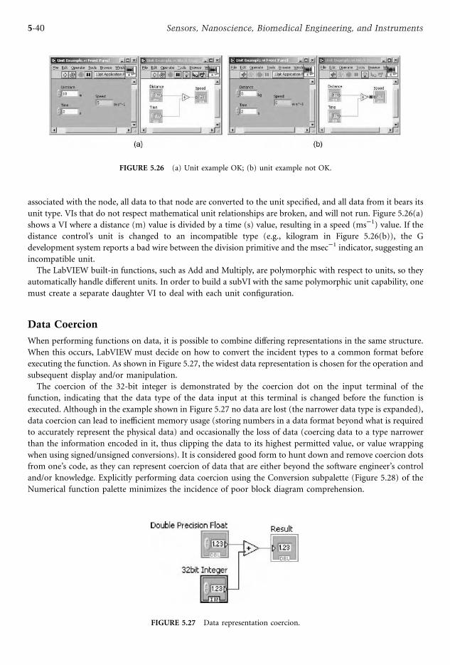
associated with the node, all data to that node are converted to the unit specified, and all data from it bears its
unit type. VIs that do not respect mathematical unit relationships are broken, and will not run. Figure 5.26(a)
shows a VI where a distance (m) value is divided by a time (s) value, resulting in a speed (ms 1) value. If the
distance control’s unit is changed to an incompatible type (e.g., kilogram in Figure 5.26(b)), the G
development system reports a bad wire between the division primitive and the msec 1 indicator, suggesting an
incompatible unit.
The LabVIEW built-in functions, such as Add and Multiply, are polymorphic with respect to units, so they
automatically handle different units. In order to build a subVI with the same polymorphic unit capability, one
must create a separate daughter VI to deal with each unit configuration.
Data Coercion
When performing functions on data, it is possible to combine differing representations in the same structure.
When this occurs, LabVIEW must decide on how to convert the incident types to a common format before
executing the function. As shown in Figure 5.27, the widest data representation is chosen for the operation and
subsequent display and/or manipulation.
The coercion of the 32-bit integer is demonstrated by the coercion dot on the input terminal of the
function, indicating that the data type of the data input at this terminal is changed before the function is
executed. Although in the example shown in Figure 5.27 no data are lost (the narrower data type is expanded),
data coercion can lead to inefficient memory usage (storing numbers in a data format beyond what is required
to accurately represent the physical data) and occasionally the loss of data (coercing data to a type narrower
than the information encoded in it, thus clipping the data to its highest permitted value, or value wrapping
when using signed/unsigned conversions). It is considered good form to hunt down and remove coercion dots
from one’s code, as they can represent coercion of data that are either beyond the software engineer’s control
and/or knowledge. Explicitly performing data coercion using the Conversion subpalette (Figure 5.28) of the
Numerical function palette minimizes the incidence of poor block diagram comprehension.
FIGURE 5.26 (a) Unit example OK; (b) unit example not OK.
FIGURE 5.27 Data representation coercion.
5-40 Sensors, Nanoscience, Biomedical Engineering, and Instruments
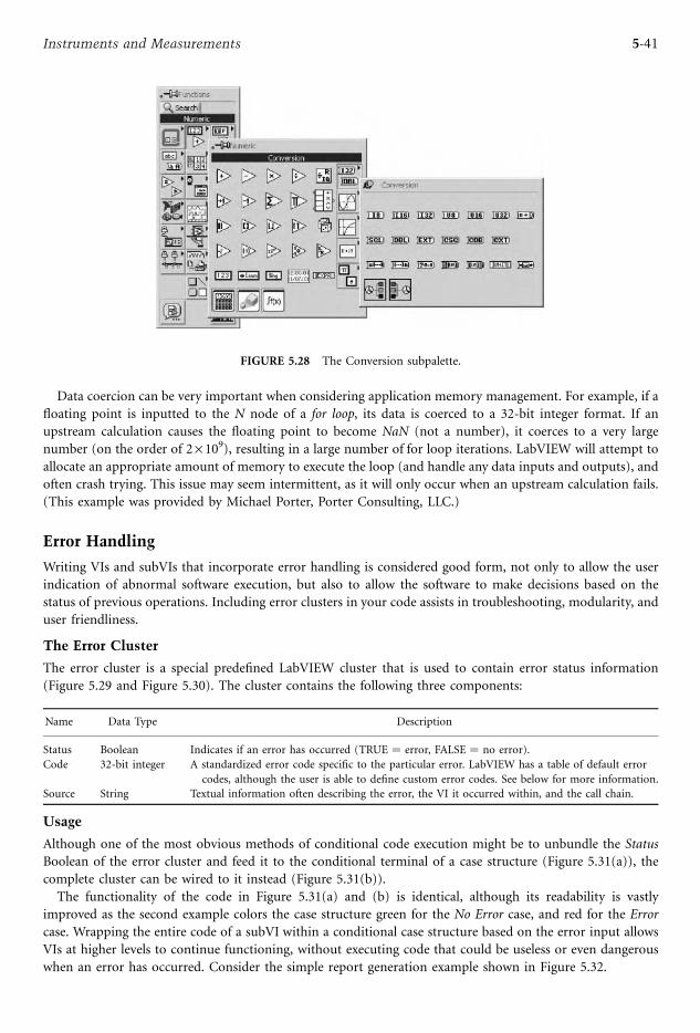
Data coercion can be very important when considering application memory management. For example, if a
floating point is inputted to the N node of a for loop, its data is coerced to a 32-bit integer format. If an
upstream calculation causes the floating point to become NaN (not a number), it coerces to a very large
number (on the order of 2· 109), resulting in a large number of for loop iterations. LabVIEW will attempt to
allocate an appropriate amount of memory to execute the loop (and handle any data inputs and outputs), and
often crash trying. This issue may seem intermittent, as it will only occur when an upstream calculation fails.
(This example was provided by Michael Porter, Porter Consulting, LLC.)
Error Handling
Writing VIs and subVIs that incorporate error handling is considered good form, not only to allow the user
indication of abnormal software execution, but also to allow the software to make decisions based on the
status of previous operations. Including error clusters in your code assists in troubleshooting, modularity, and
user friendliness.
The Error Cluster
The error cluster is a special predefined LabVIEW cluster that is used to contain error status information
(Figure 5.29 and Figure 5.30). The cluster contains the following three components:
Name Data Type Description
Status Boolean Indicates if an error has occurred (TRUE ¼ error, FALSE ¼ no error).
Code 32-bit integer A standardized error code specific to the particular error. LabVIEW has a table of default error
codes, although the user is able to define custom error codes. See below for more information.
Source String Textual information often describing the error, the VI it occurred within, and the call chain.
Usage
Although one of the most obvious methods of conditional code execution might be to unbundle the Status
Boolean of the error cluster and feed it to the conditional terminal of a case structure (Figure 5.31(a)), the
complete cluster can be wired to it instead (Figure 5.31(b)).
The functionality of the code in Figure 5.31(a) and (b) is identical, although its readability is vastly
improved as the second example colors the case structure green for the No Error case, and red for the Error
case. Wrapping the entire code of a subVI within a conditional case structure based on the error input allows
VIs at higher levels to continue functioning, without executing code that could be useless or even dangerous
when an error has occurred. Consider the simple report generation example shown in Figure 5.32.
FIGURE 5.28 The Conversion subpalette.
5-41Instruments and Measurements
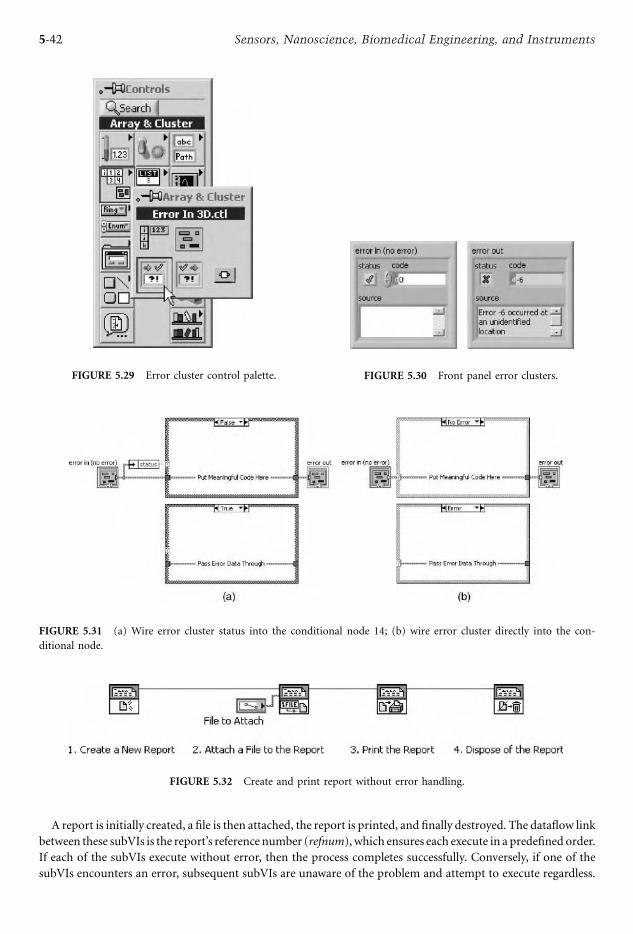
A report is initially created, a file is then attached, the report is printed, and finally destroyed. The dataflow link
between these subVIs is the report’s reference number (refnum), which ensures each execute in a predefined order.
If each of the subVIs execute without error, then the process completes successfully. Conversely, if one of the
subVIs encounters an error, subsequent subVIs are unaware of the problem and attempt to execute regardless.
FIGURE 5.29 Error cluster control palette. FIGURE 5.30 Front panel error clusters.
FIGURE 5.31 (a) Wire error cluster status into the conditional node 14; (b) wire error cluster directly into the con-
ditional node.
FIGURE 5.32 Create and print report without error handling.
5-42 Sensors, Nanoscience, Biomedical Engineering, and Instruments
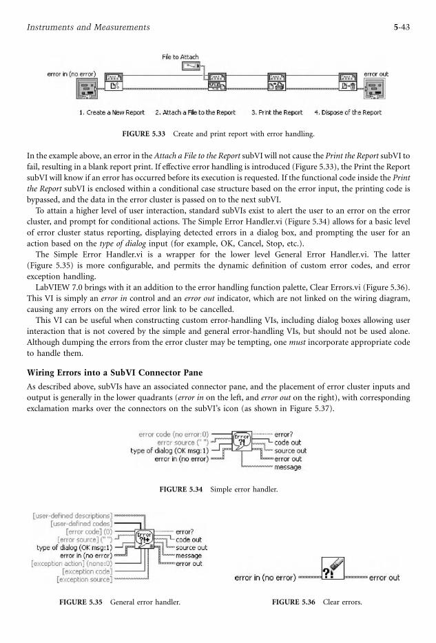
In the example above, an error in the Attach a File to the Report subVIwill not cause the Print the Report subVI to
fail, resulting in a blank report print. If effective error handling is introduced (Figure 5.33), the Print the Report
subVI will know if an error has occurred before its execution is requested. If the functional code inside the Print
the Report subVI is enclosed within a conditional case structure based on the error input, the printing code is
bypassed, and the data in the error cluster is passed on to the next subVI.
To attain a higher level of user interaction, standard subVIs exist to alert the user to an error on the error
cluster, and prompt for conditional actions. The Simple Error Handler.vi (Figure 5.34) allows for a basic level
of error cluster status reporting, displaying detected errors in a dialog box, and prompting the user for an
action based on the type of dialog input (for example, OK, Cancel, Stop, etc.).
The Simple Error Handler.vi is a wrapper for the lower level General Error Handler.vi. The latter
(Figure 5.35) is more configurable, and permits the dynamic definition of custom error codes, and error
exception handling.
LabVIEW 7.0 brings with it an addition to the error handling function palette, Clear Errors.vi (Figure 5.36).
This VI is simply an error in control and an error out indicator, which are not linked on the wiring diagram,
causing any errors on the wired error link to be cancelled.
This VI can be useful when constructing custom error-handling VIs, including dialog boxes allowing user
interaction that is not covered by the simple and general error-handling VIs, but should not be used alone.
Although dumping the errors from the error cluster may be tempting, one must incorporate appropriate code
to handle them.
Wiring Errors into a SubVI Connector Pane
As described above, subVIs have an associated connector pane, and the placement of error cluster inputs and
output is generally in the lower quadrants (error in on the left, and error out on the right), with corresponding
exclamation marks over the connectors on the subVI’s icon (as shown in Figure 5.37).
FIGURE 5.33 Create and print report with error handling.
FIGURE 5.34 Simple error handler.
FIGURE 5.35 General error handler. FIGURE 5.36 Clear errors.
5-43Instruments and Measurements
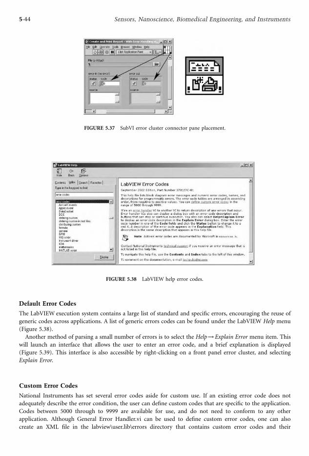
Default Error Codes
The LabVIEW execution system contains a large list of standard and specific errors, encouraging the reuse of
generic codes across applications. A list of generic errors codes can be found under the LabVIEW Help menu
(Figure 5.38).
Another method of parsing a small number of errors is to select the Help! Explain Error menu item. This
will launch an interface that allows the user to enter an error code, and a brief explanation is displayed
(Figure 5.39). This interface is also accessible by right-clicking on a front panel error cluster, and selecting
Explain Error.
Custom Error Codes
National Instruments has set several error codes aside for custom use. If an existing error code does not
adequately describe the error condition, the user can define custom codes that are specific to the application.
Codes between 5000 through to 9999 are available for use, and do not need to conform to any other
application. Although General Error Handler.vi can be used to define custom error codes, one can also
create an XML file in the labview\user.lib\errors directory that contains custom error codes and their
FIGURE 5.37 SubVI error cluster connector pane placement.
FIGURE 5.38 LabVIEW help error codes.
5-44 Sensors, Nanoscience, Biomedical Engineering, and Instruments
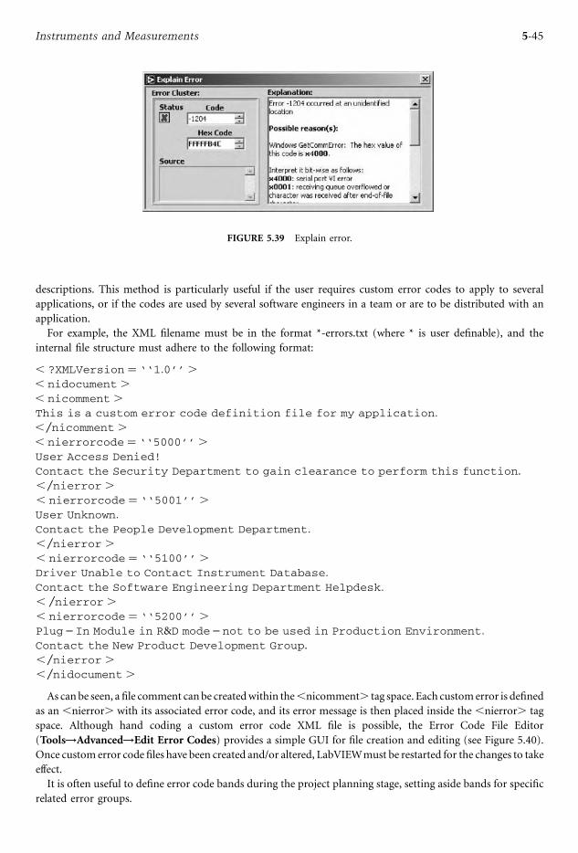
descriptions. This method is particularly useful if the user requires custom error codes to apply to several
applications, or if the codes are used by several software engineers in a team or are to be distributed with an
application.
For example, the XML filename must be in the format *-errors.txt (where * is user definable), and the
internal file structure must adhere to the following format:
, ?XMLVersion ¼ ‘‘1:0’’ .
, nidocument .
, nicomment .
This is a custom error code definition file for my application:
,=nicomment .
, nierrorcode ¼ ‘‘5000’’ .
User Access Denied!
Contact the Security Department to gain clearance to perform this function.
,=nierror .
, nierrorcode ¼ ‘‘5001’’ .
User Unknown:
Contact the People Development Department:
,=nierror .
, nierrorcode ¼ ‘‘5100’’ .
Driver Unable to Contact Instrument Database:
Contact the Software Engineering Department Helpdesk:
, =nierror .
, nierrorcode ¼ ‘‘5200’’ .
Plug In Module in R&D mode not to be used in Production Environment:
Contact the New Product Development Group.
,=nierror .
,=nidocument .
As can be seen, a file comment can be createdwithin the,nicomment. tag space. Each customerror is defined
as an ,nierror. with its associated error code, and its error message is then placed inside the ,nierror. tag
space. Although hand coding a custom error code XML file is possible, the Error Code File Editor
(Tools!Advanced!Edit Error Codes) provides a simple GUI for file creation and editing (see Figure 5.40).
Once custom error code files have been created and/or altered, LabVIEWmust be restarted for the changes to take
effect.
It is often useful to define error code bands during the project planning stage, setting aside bands for specific
related error groups.
FIGURE 5.39 Explain error.
5-45Instruments and Measurements
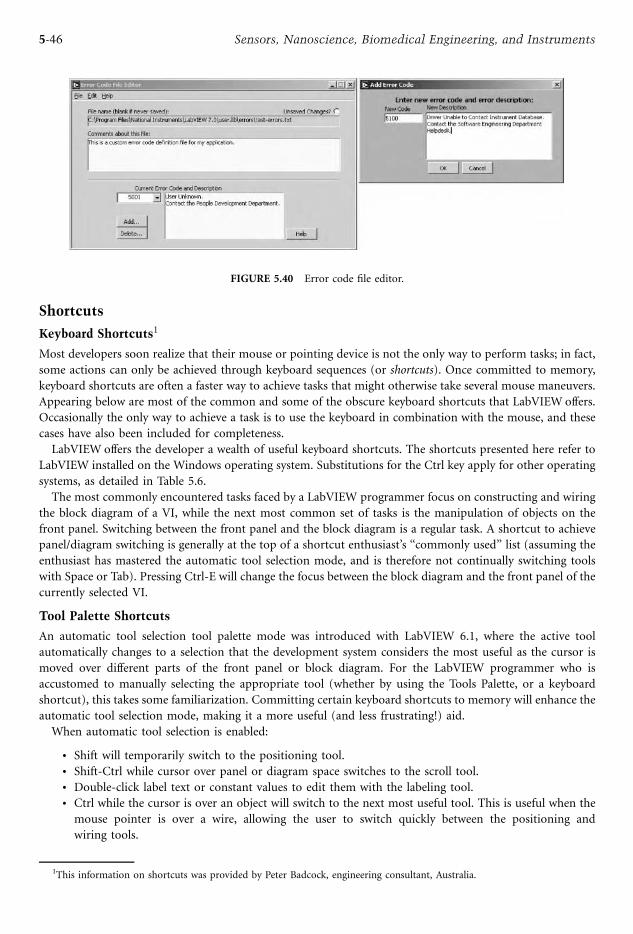
Shortcuts
Keyboard Shortcuts1
Most developers soon realize that their mouse or pointing device is not the only way to perform tasks; in fact,
some actions can only be achieved through keyboard sequences (or shortcuts). Once committed to memory,
keyboard shortcuts are often a faster way to achieve tasks that might otherwise take several mouse maneuvers.
Appearing below are most of the common and some of the obscure keyboard shortcuts that LabVIEW offers.
Occasionally the only way to achieve a task is to use the keyboard in combination with the mouse, and these
cases have also been included for completeness.
LabVIEW offers the developer a wealth of useful keyboard shortcuts. The shortcuts presented here refer to
LabVIEW installed on the Windows operating system. Substitutions for the Ctrl key apply for other operating
systems, as detailed in Table 5.6.
The most commonly encountered tasks faced by a LabVIEW programmer focus on constructing and wiring
the block diagram of a VI, while the next most common set of tasks is the manipulation of objects on the
front panel. Switching between the front panel and the block diagram is a regular task. A shortcut to achieve
panel/diagram switching is generally at the top of a shortcut enthusiast’s ‘‘commonly used’’ list (assuming the
enthusiast has mastered the automatic tool selection mode, and is therefore not continually switching tools
with Space or Tab). Pressing Ctrl-E will change the focus between the block diagram and the front panel of the
currently selected VI.
Tool Palette Shortcuts
An automatic tool selection tool palette mode was introduced with LabVIEW 6.1, where the active tool
automatically changes to a selection that the development system considers the most useful as the cursor is
moved over different parts of the front panel or block diagram. For the LabVIEW programmer who is
accustomed to manually selecting the appropriate tool (whether by using the Tools Palette, or a keyboard
shortcut), this takes some familiarization. Committing certain keyboard shortcuts to memory will enhance the
automatic tool selection mode, making it a more useful (and less frustrating!) aid.
When automatic tool selection is enabled:
. Shift will temporarily switch to the positioning tool.
. Shift-Ctrl while cursor over panel or diagram space switches to the scroll tool.
. Double-click label text or constant values to edit them with the labeling tool.
. Ctrl while the cursor is over an object will switch to the next most useful tool. This is useful when the
mouse pointer is over a wire, allowing the user to switch quickly between the positioning and
wiring tools.
1This information on shortcuts was provided by Peter Badcock, engineering consultant, Australia.
FIGURE 5.40 Error code file editor.
5-46 Sensors, Nanoscience, Biomedical Engineering, and Instruments

Note that Shift-Tab enables and disables the automatic tool selection mode.
When automatic tool selection is disabled:
. Tab selects the next tool on the tools palette.
. Space toggles between the positioning tool and the scrolling tool on the front panel, or the positioning
tool and the wiring tool on the block diagram.
Miscellaneous Front Panel and Block Diagram Shortcuts
To create additional space in the selection, Ctrl-click (for operating systems other than Windows, use
ShiftþCtrlþClick) from a clear point on the panel or diagram and select an area. The cursor keys ( , ",!, #)nudge selections 1 pixel in the direction chosen, whereas simultaneously holding down Shift while moving a
selection with a cursor key increases the distance moved to 8 pixels. Other miscellaneous shortcuts include
those listed in Table 5.7.
General Shortcuts
A complete list of keyboard shortcuts for the main pull-down menus can be found on the LabVIEW Quick
Reference Card (shipped with LabVIEW and accessible in the online help). Some commonly used keyboard
shortcuts include those shown in Table 5.8.
GOOP
G is well known for its speed of code development that provides engineers with a rapid prototyping advantage.
This advantage is particularly evident when working with small projects with flat structures. However, as
project complexity grows, initial stages of software architecture planning become vitally important.
GOOP (graphical object-oriented programming) is a method for developing object-oriented code, and is
created using an external object model (often referred to as ‘‘LabVIEW external object’’ oriented
programming, or LEO). Using GOOP has three main advantages to application development: code
maintainability, scalability, and reusability. GOOP is the most common form of OOP with LabVIEW, and has
been used successfully in many commercially available applications developed by G software engineers.
By implementing GOOP classes, you can take advantage of standard OOP analysis and design tools,
including Microsoft Visual Modeler, and apply principles that describe object-oriented design and
TABLE 5.6 Control Key Substitutions across LabVIEW-Supported Platforms
Operating System Control Key
WindowsTM Ctrl
MacintoshTM Option or Command (context dependent)
SunTM/UNIX1 Meta
LinuxTM/HP-UXTM Alt
TABLE 5.7 Other Miscellaneous Shortcuts
Shortcut Description
Ctrl-double click On a clear point, places text (otherwise known as a free label)
Shift-right click Displays the tool palette
Ctrl-double click On a sub VI, opens its block diagram
Ctrl-click-drag An object with the positioning tool to duplicate it
Shift-click The block diagram to remove the last wiring point
Esc Cancels a wire route (dashed)
Ctrl-B Removes broken wires (Beware: nonvisible broken wires may exist)
Drag-space Activate autowiring when moving an element on the block diagram (Autowiring only occurs when
first placing an element, or a copy of an element, on the block diagram)
5-47Instruments and Measurements
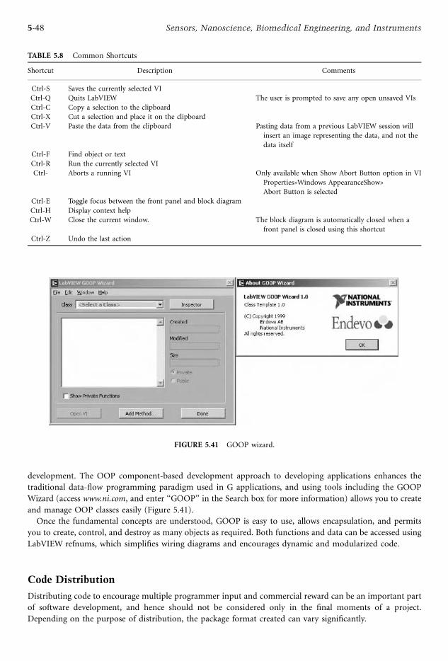
development. The OOP component-based development approach to developing applications enhances the
traditional data-flow programming paradigm used in G applications, and using tools including the GOOP
Wizard (access www.ni.com, and enter ‘‘GOOP’’ in the Search box for more information) allows you to create
and manage OOP classes easily (Figure 5.41).
Once the fundamental concepts are understood, GOOP is easy to use, allows encapsulation, and permits
you to create, control, and destroy as many objects as required. Both functions and data can be accessed using
LabVIEW refnums, which simplifies wiring diagrams and encourages dynamic and modularized code.
Code Distribution
Distributing code to encourage multiple programmer input and commercial reward can be an important part
of software development, and hence should not be considered only in the final moments of a project.
Depending on the purpose of distribution, the package format created can vary significantly.
TABLE 5.8 Common Shortcuts
Shortcut Description Comments
Ctrl-S Saves the currently selected VI
Ctrl-Q Quits LabVIEW The user is prompted to save any open unsaved VIs
Ctrl-C Copy a selection to the clipboard
Ctrl-X Cut a selection and place it on the clipboard
Ctrl-V Paste the data from the clipboard Pasting data from a previous LabVIEW session will
insert an image representing the data, and not the
data itself
Ctrl-F Find object or text
Ctrl-R Run the currently selected VI
Ctrl- Aborts a running VI Only available when Show Abort Button option in VI
Properties»Windows AppearanceShow»
Abort Button is selected
Ctrl-E Toggle focus between the front panel and block diagram
Ctrl-H Display context help
Ctrl-W Close the current window. The block diagram is automatically closed when a
front panel is closed using this shortcut
Ctrl-Z Undo the last action
FIGURE 5.41 GOOP wizard.
5-48 Sensors, Nanoscience, Biomedical Engineering, and Instruments

llbs
A VI library (*.llb) is a National Instruments proprietary file that can contain several VIs and some of their
settings. Files that are saved into an llb are lightly compressed, and can be set as top level (denotes which VIs
should be launched when their respective llb is opened) or companion. Other than that, an llb is formless; all of
the files reside at one level (i.e., you cannot create subdirectories or sub-llbs in a VI library). Although a library
has a flat structure, it is possible to assign one of two levels to a VI in a library. A top-level VI will launch
automatically when opened from your operating system’s file explorer, whereas a normal-level VI will only
open if explicitly opened from within the library. (A new feature to LabVIEW 7.0 allows Windows Explorer to
navigate inside G libraries, effectively bypassing top-level assignments.) It is also acceptable to assign more
than one VI in a library as top level, although this can make window negotiation difficult, as they all will be
launched when the library is opened. Figure 5.42 demonstrates a library with one top-level VI.
Development Distribution Library
A development distribution library contains all custom VIs and controls that have been created in the project,
so that it can be successfully opened and executed on a PC with a similar LabVIEW configuration installed. VIs
from vi.lib and add-on toolkits are not included in a development library, as it is assumed that environments
used for subsequent openings of the library will have these installed.
Application Distribution Library
An application distribution library is an llb file that contains all of the VIs listed in a development library, and
all others that are used in the application. VIs from vi.lib and toolkits are included, as are all custom VIs and
controls. Distributing an application library is useful when archiving an application, including all of the
components used to execute it.
Diagram Access
Altering a user’s access to a VI’s diagram can minimize code theft and ensure that the VIs are opened with an
appropriate version of LabVIEW. Setting a password to a VI’s block diagram prevents users from accessing the
code diagram and understanding hierarchical dependencies between modules. To change a VI’s status, access
the Security VI property (Figure 5.43) and select one of the settings shown in Table 5.9.
An extreme method of code protection is to remove the block diagram altogether, and can be achieved by
performing a custom save (Figure 5.44), using File ! Save with Options.
FIGURE 5.42 A library with a top-level VI.
5-49Instruments and Measurements
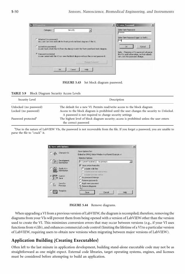
Whenupgrading aVI from a previous version of LabVIEW, the diagram is recompiled; therefore, removing the
diagrams from your VIs will prevent them from being opened with a version of LabVIEWother than the version
used to create the VI. This minimizes conversion errors that may occur between versions (e.g., if your VI uses
functions fromvi.lib), and enhances commercial code control (limiting the lifetime of a VI to a particular version
of LabVIEW, requiring users to obtain new versions when migrating between major versions of LabVIEW).
Application Building (Creating Executables)
Often left to the last minute in application development, building stand-alone executable code may not be as
straightforward as one might expect. External code libraries, target operating systems, engines, and licenses
must be considered before attempting to build an application.
FIGURE 5.43 Set block diagram password.
TABLE 5.9 Block Diagram Security Access Levels
Security Level Description
Unlocked (no password) The default for a new VI. Permits read/write access to the block diagram
Locked (no password) Access to the block diagram is prohibited until the user changes the security to Unlocked.
A password is not required to change security settings
Password protecteda The highest level of block diagram security; access is prohibited unless the user enters
the correct password
aDue to the nature of LabVIEW VIs, the password is not recoverable from the file. If you forget a password, you are unable toparse the file to ‘‘crack’’ it.
FIGURE 5.44 Remove diagrams.
5-50 Sensors, Nanoscience, Biomedical Engineering, and Instruments
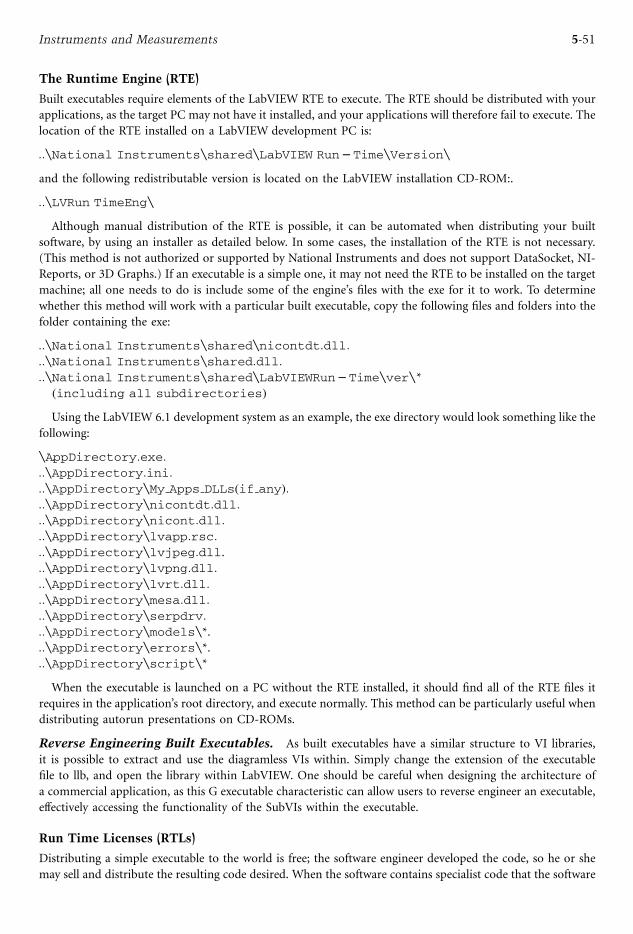
The Runtime Engine (RTE)
Built executables require elements of the LabVIEW RTE to execute. The RTE should be distributed with your
applications, as the target PC may not have it installed, and your applications will therefore fail to execute. The
location of the RTE installed on a LabVIEW development PC is:
::nNational InstrumentsnsharednLabVIEW Run TimenVersionnand the following redistributable version is located on the LabVIEW installation CD-ROM:.
::nLVRun TimeEngnAlthough manual distribution of the RTE is possible, it can be automated when distributing your built
software, by using an installer as detailed below. In some cases, the installation of the RTE is not necessary.
(This method is not authorized or supported by National Instruments and does not support DataSocket, NI-
Reports, or 3D Graphs.) If an executable is a simple one, it may not need the RTE to be installed on the target
machine; all one needs to do is include some of the engine’s files with the exe for it to work. To determine
whether this method will work with a particular built executable, copy the following files and folders into the
folder containing the exe:
::nNational Instrumentsnsharednnicontdt:dll:::nNational Instrumentsnshared:dll:::nNational InstrumentsnsharednLabVIEWRun Timenvern*ðincluding all subdirectoriesÞUsing the LabVIEW 6.1 development system as an example, the exe directory would look something like the
following:
.nAppDirectory:exe:::nAppDirectory:ini:::nAppDirectorynMy Apps DLLsðif anyÞ:::nAppDirectorynnicontdt:dll:::nAppDirectorynnicont:dll:::nAppDirectorynlvapp:rsc:::nAppDirectorynlvjpeg:dll.::nAppDirectorynlvpng:dll:::nAppDirectorynlvrt:dll:::nAppDirectorynmesa:dll:::nAppDirectorynserpdrv:::nAppDirectorynmodelsn*.::nAppDirectorynerrorsn*.::nAppDirectorynscriptn*When the executable is launched on a PC without the RTE installed, it should find all of the RTE files it
requires in the application’s root directory, and execute normally. This method can be particularly useful when
distributing autorun presentations on CD-ROMs.
Reverse Engineering Built Executables. As built executables have a similar structure to VI libraries,
it is possible to extract and use the diagramless VIs within. Simply change the extension of the executable
file to llb, and open the library within LabVIEW. One should be careful when designing the architecture of
a commercial application, as this G executable characteristic can allow users to reverse engineer an executable,
effectively accessing the functionality of the SubVIs within the executable.
Run Time Licenses (RTLs)
Distributing a simple executable to the world is free; the software engineer developed the code, so he or she
may sell and distribute the resulting code desired. When the software contains specialist code that the software
5-51Instruments and Measurements
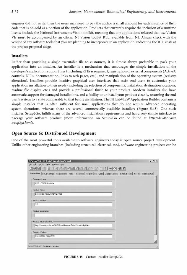
engineer did not write, then the users may need to pay the author a small amount for each instance of their
code that is on-sold as a portion of the application. Products that currently require the inclusion of a runtime
license include the National Instruments Vision toolkit, meaning that any applications released that use Vision
VIs must be accompanied by an official NI Vision toolkit RTL, available from NI. Always check with the
vendor of any software tools that you are planning to incorporate in an application, indicating the RTL costs at
the project proposal stage.
Installers
Rather than providing a single executable file to customers, it is almost always preferable to pack your
application into an installer. An installer is a mechanism that encourages the simple installation of the
developer’s application, support files (including RTEs is required), registration of external components (ActiveX
controls, DLLs, documentation, links to web pages, etc.), and manipulation of the operating system (registry
alteration). Installers provide intuitive graphical user interfaces that assist end users to customize your
application installation to their needs (including the selection of components, installation destination locations,
readme file display, etc.) and provide a professional finish to your product. Modern installers also have
automatic support for damaged installations, and a facility to uninstall your product cleanly, returning the end
user’s system to a state comparable to that before installation. The NI LabVIEWApplication Builder contains a
simple installer that is often sufficient for small applications that do not require advanced operating
system alterations, whereas there are several commercially available installers (Figure 5.45). One such
installer, Setup2Go, fulfills many of the advanced installation requirements and has a very simple interface to
package your software product (more information on Setup2Go can be found at http://dev4pc.com/
setup2go.html).
Open Source G: Distributed Development
One of the most powerful tools available to software engineers today is open source project development.
Unlike other engineering branches (including structural, electrical, etc.), software engineering projects can be
FIGURE 5.45 Custom installer Setup2Go.
5-52 Sensors, Nanoscience, Biomedical Engineering, and Instruments

easily transported to all corners of the earth in seconds using the Internet. Using this unique ability, projects
can be developed at many different sites by several professionals simultaneously, ultimately leading to better
tested software with extended features and more robust code. Sharing the burden of developing a software
project allows engineers a much wider range of experience and expertise, and thus a more stable and useful
application.
As you might imagine, coordinating such projects can be time intensive and legally difficult, which is why
the OpenG community has been created. Spearheaded by the longtime LabVIEWexpert Jim Kring, OpenG.org
(Figure 5.46) is the home of our Open Source LabVIEWdevelopment community, hosting the largest registry
of Open Source LabVIEW code and applications available on the Internet. OpenG.org is a not-for-profit
venture, and provides each project a web page, where you can embed HTML, allowing you to link to software
and websites, as well as embed images and other content hosted remotely.
All OpenG.org projects are covered by the LGPL software license, which protects source code, so that it
remains Open Source, but it allows using protected code in commercial, proprietary, closed applications. Most
people using LabVIEW are using it directly in commercial or industrial applications and systems that are
sensitive because they contain intellectual property in the form of valuable trade secrets. The ideals of the
OpenG community promote the adoption of open source everywhere that LabVIEW is used.
More information on the OpenG project, and how to develop software using open source principles is
available at the OpenG website (www.openg.org) (Figure 5.46).
Defining Terms
Block (wiring) diagram: The coding portion of a VI, where the software engineer writes the G code.
Data type: The format the G development system uses to store a piece of information in memory. Using
appropriate data types decreases application execution time, decreases memory footprint, and
eradicates coercion errors.
FIGURE 5.46 OpenG website.
5-53Instruments and Measurements

Error cluster: A special cluster containing an error code, a Boolean indicating if an error has occurred, and
the source of that error. The error cluster format is consistent throughout the G development system.
Front panel: The graphical user interface of a VI, including a method in which data are passed to and from
the VI.
G: The programming language used to develop applications using the LabVIEW Development System.
Installer: Software that facilitates the automatic installation, upgrade, repair, or uninstallation of third-
party software.
LabVIEW: The development system used to develop code in the G programming language.
Polymorphic VI: A collection of VIs with identical missions, operating on differing data types. A
polymorphic VI exists on disk as a special form of a VI library.
Runtime engine (RTE): The system under which compiled G code runs, without the presence of the G
development system.
Runtime license (RTL): A ‘‘user pays’’ system of charging for code portion development.
Unit: An attribute associated with a numerical value, giving it physical significance.
Further Information
National Instruments, www.ni.com/labview (G development system vendor)
National Instruments Alliance Members (system integrators), www.ni.com/alliance
The LabVIEW Zone, www.ni.com/labviewzone (developer forum)
OpenG—Open Source G Development, www.openg.org (developer forum)
InfoLabVIEW Mailing List, www.info-labview.org (developer forum)
LabVIEW Technical Resource, www.ltrpub.com (journal)
5-54 Sensors, Nanoscience, Biomedical Engineering, and Instruments

6Reliability Engineering
B.S. DhillonUniversity of Ottawa
6.1 Introduction ........................................................................ 6-1
6.2 Terms and Definitions........................................................... 6-2
6.3 Bathtub Hazard-Rate Concept ................................................ 6-2
6.4 Important Formulas ............................................................. 6-3Reliability * Mean Time to Failure * Hazard Rate
6.5 Reliability Networks .............................................................. 6-5Series Network * Parallel Network * k-out–of-m Network
6.6 Reliability Evaluation Methods ............................................... 6-8Failure Modes and Effect Analysis * Fault-Tree Analysis *
The Markov Method
6.7 Human Reliability .............................................................. 6-13Classification and Causes of Human Errors * Human
Reliability Measures * Modeling Human Operation in a
Fluctuating Environment
6.8 Robot Reliability ................................................................ 6-16Robot Failure Classifications and Causes * Robot Reliability
Measures
6.1 Introduction
Reliability is an important consideration in the planning, design, and operation of engineering systems.
The benefits of reliable systems are enormous and include a reduction in unexpected failures, lower main-
tenance costs, lower life-cycle costs, improved safety, less need for in-process inventory to cover downtime and
more consistent quality [1,2]. Prior to World War II, the concept of reliability had been intuitive, subjective,
and qualitative. Today, it is a well-recognized discipline with many specialized areas, including that of human
reliability, robot reliability, software reliability, and mechanical reliability.
The reliability field is generally regarded as having started before World War II, with the development of V1
and V2 rockets in Germany. In 1950, the U.S. Department of Defense established an ad-hoc committee on
reliability, and in 1952 it became known as the Advisory Group on the Reliability of Electronic Equipment
(AGREE). In 1957, AGREE released a report that helped specificy the reliability of military electronic
equipment [3,4].
In 1951, W. Weibull developed a statistical distribution that has played an important role in the
development of the reliability field [5]. The first book on reliability, titled Reliability Factors for Ground
Electronic Equipment, was published in 1956 [6]. Since then, more than 100 books on reliability have been
published, as well as thousands of articles. Today, many scientific journals are totally or partially devoted
to the reliability field. Refs. [7,8] provide a comprehensive list of publications on reliability and associated
topics.
This chapter presents some important aspects of reliability.
6-1

6.2 Terms and Definitions
There are many terms and definitions in the reliability discipline and most can be found in Refs. [9–11]. Some
commonly used terms and definitions are as follows [12–14]:
. Reliability: The probability that an item will conclude its mission satisfactorily for the stated period
when used under the specified conditions.. Failure: An item’s inability to perform within the defined guidelines.. Hazard rate: The quantity of the rate of change for the failed items over the number of survived items
at time t.. Mean time to failure (exponential distribution): The sum of the operating time of given items over
the total number of failures.. Availability: The probability that an item is available for use when required.. Redundancy: The existence of two or more means for performing a required function.. Human error: The failure to perform a specified task (or the performance of a forbidden action) that
could disrupt scheduled operations or damage equipment or property.. Steady-state condition (statistical): The condition where the probability of being in a certain state is
independent of time.. Random failure: A failure that cannot be predicted.. Repair rate: A figure-of-merit that measures repair capability. In the case of exponential distribution, it
is the reciprocal of mean time to repair.
6.3 Bathtub Hazard-Rate Concept
This concept often is used when performing a reliability analysis of engineering items, primarily for electronic
parts. In this case, one assumes that an item’s hazard rate or time-dependent failure rate follows a curve
resembling the shape of a bathtub. A bathtub hazard-rate curve is shown in Figure 6.1. The curve in the figure
can be divided into three parts: infant mortality period, useful life period, and wear-out period. In the infant-
mortality period, the hazard rate decreases over time. Other names to describe this period are ‘‘burn-in
period,’’ ‘‘debugging period’’, and ‘‘break-in period.’’ Causes for failures in this period include inadequate test
specifications, ineffective quality control, marginal components, unsatisfactory manufacturing processes or
tooling, overstressed parts, improper use procedures, inadequate materials, and improper handling or
packaging [15].
During the useful life period, the hazard rate remains constant. Failures during this period are known as
‘‘random failures’’ because they occur unpredictably. Failures during the useful life period can be caused by
inadequate design margins, wrong applications, and usage in the wrong environment.
Infant mortalityperiod
Hazardrate
0 Time
Useful life period Wear-out period
FIGURE 6.1 A bathtub hazard-rate curve.
6-2 Sensors, Nanoscience, Biomedical Engineering, and Instruments

In the wear-out period, the hazard rate increases over time and starts when an item has ended its useful life.
Wear-out failures can be caused by material wear, unsatisfactory or improper preventative maintenance,
scratching, misalignments, aging, limited-life parts, loose hardware, or incipient stress.
The following function can represent the bathtub hazard-rate curve [16]:
lðtÞ ¼ klntn 1 þ ð1 kÞbtb 1yeytb
for ¼ y; n; b; l > 0; 0< k< 1; t > 0 ð6:1Þwhere l(t) is the hazard rate (i.e., failure rate at time t), l and y are the scale parameters, and b and n are theshape parameters.
At n ¼ 0.5 and b ¼ 1, Equation (6.1) gives the bathtub hazard-rate curve. The hazard-rate functions
of exponential, Rayleigh, Weibull, Makeham, and extreme-value distributions are special cases of
Equation (6.1).
6.4 Important Formulas
Reliability work includes many frequently used mathematical formulas. This section presents formulas for
achieving reliability, mean time to failure and an item’s hazard rate.
Reliability
This is defined by
RðtÞ ¼ 1Zt0
f ðtÞdt ð6:2Þ
or
RðtÞ ¼ eZt0
lðtÞdt ð6:3Þ
or
RðtÞ ¼Z1t
f ðtÞdt ð6:4Þ
where R(t) is reliability at time t, f(t) is the probability or failure-density function, and l(t) is the hazard ortime-dependent failure rate.
Example 1
Assume that the failure rate of a manufacturing system is 0.0004 failures per hour. Calculate the system
reliability for a 10-hour mission.
By substituting the given data into Equation (6.3), we get
RðtÞ ¼ eZt0
ð0:0004Þdt
¼ e ð0:0004Þt
¼ e ð0:0004Þð10Þ
¼ 0:9960
The result is a 99.6% chance that the manufacturing system will not fail during the specified period.
6-3Reliability Engineering
Mean Time to Failure
An item’s mean time to failure (MTTF) can be calculated by using any of the following three formulas:
MTTF ¼Z10
RðtÞdt ð6:5Þ
or
MTTF ¼Z10
tf ðtÞdt ð6:6Þ
MTTF ¼ lims!0
RðsÞ ð6:7Þ
where s is the Laplace transform variable and R(s) is the Laplace transform of R(t).
Example 2
In Example 1, find the mean time to failure of the manufacturing system.
By using the data in Equation (6.3) we find:
RðtÞ ¼ e ð0:0004Þt ð6:8Þ
Inserting Equation (6.7) into Equation (6.5) yields:
MTTF ¼Z10
e ð0:0004Þtdt
¼ 1
0:0004
¼ 2;500 hours
The mean time to failure of the manufacturing system is 2500 h.
Hazard Rate
This can be defined as
lðtÞ ¼ f ðtÞRðtÞ ð6:9Þ
or
lðtÞ ¼ f ðtÞR1t
f ðtÞdtð6:10Þ
or
lðtÞ ¼ f ðtÞ1
Rt0
f ðtÞdtð6:11Þ
6-4 Sensors, Nanoscience, Biomedical Engineering, and Instruments

or
lðtÞ ¼ 1
RðtÞdRðtÞdt
ð6:12ÞExample 3
Assume that the time to failure for a machine tool is described by the following probability density
function:
f ðtÞ ¼ le lt ð6:13Þwhere l is the distribution parameter.Obtain an expression for the machine-tool hazard rate.
By substituting Equation (6.13) into Equation (6.4), we get:
RðtÞ ¼Z1t
le ltdt
¼ e lt
ð6:14Þ
Using Equation (6.13) and Equation (6.14) in Equation (6.9) yields:
lðtÞ ¼ le lt
e lt
¼ lð6:15Þ
The above expression is used to find the machine-tool hazard rate and is independent of time. Usually, the
hazard rate under this condition is known as the failure rate.
6.5 Reliability Networks
In reliability analysis, engineering systems can form various networks or configurations. Some commonly
occurring configurations are that of series, parallel, and k-out-of-m. Each of these configurations is discussed
below.
Series Network
In this case, if any n unit fails, the system fails. All system units must work normally for the system to succeed.
Figure 6.2 shows the block diagram of a series network.
For independent units, the reliability of the series network is given by:
Rs ¼ R1R2R3 . . .Rn ð6:16Þwhere Rs is the series system reliability and Ri is the unit i reliability; for i ¼ 1, 2, 3, . . . , n.
1 2 3 n
FIGURE 6.2 An n-unit series network.
6-5Reliability Engineering

For constant failure rate of unit i, i.e., li(t) ¼ li, the unit i reliability from Equation (6.3) is
RiðtÞ ¼ e lit ð6:17Þwhere Ri(t) is the unit i reliability at time t and li is the unit i failure rate.For constant failure rates of all series units, by substituting Equation (6.17) into Equation (6.16), we get the
following expression for the series-system, time-dependent reliability:
RsðtÞ ¼ e l1te l2te l3t . . . e lnt ð6:18Þwhere Rs(t) is the series system reliability at time t.
Using Equation (6.18) in Equation (6.5), we get the following expression for the series-system mean time to
failure:
MTTFs ¼Z10
e
Pni¼1
l1tdt
¼ 1Pni¼1
li
ð6:19Þ
Example 4
Assume that an aircraft has two independent engines and both of them must operate normally for the aircraft
to fly successfully. The reliabilities of engines 1 and 2 are 0.95 and 0.98, respectively. Calculate the reliability of
the aircraft with respect to the engines.
Substituting the given data into Equation (6.16) yields:
Rs ¼ ð0:95Þð0:98Þ¼ 0:9310
There is a 93.1% chance that the aircraft will fly successfully.
Parallel Network
In this case, all units are active, and at least one must operate normally for the system to succeed. The parallel-
network block diagram is shown in Figure 6.3.
2
1
3
m
FIGURE 6.3 An m-unit parallel system.
6-6 Sensors, Nanoscience, Biomedical Engineering, and Instruments
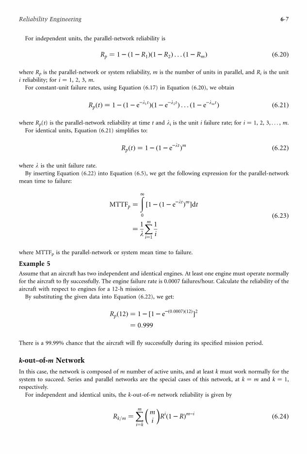
For independent units, the parallel-network reliability is
Rp ¼ 1 ð1 R1Þð1 R2Þ . . . ð1 RmÞ ð6:20Þ
where Rp is the parallel-network or system reliability, m is the number of units in parallel, and Ri is the unit
i reliability; for i ¼ 1, 2, 3, m.
For constant-unit failure rates, using Equation (6.17) in Equation (6.20), we obtain
RpðtÞ ¼ 1 ð1 e l1tÞð1 e l2tÞ . . . ð1 e lmtÞ ð6:21Þ
where Rp(t) is the parallel-network reliability at time t and li is the unit i failure rate; for i ¼ 1, 2, 3, . . . , m.
For identical units, Equation (6.21) simplifies to:
RpðtÞ ¼ 1 ð1 e ltÞm ð6:22Þ
where l is the unit failure rate.By inserting Equation (6.22) into Equation (6.5), we get the following expression for the parallel-network
mean time to failure:
MTTFp ¼Z10
½1 ð1 e ltÞm dt
¼ 1
l
Xmi¼1
1
i
ð6:23Þ
where MTTFp is the parallel-network or system mean time to failure.
Example 5
Assume that an aircraft has two independent and identical engines. At least one engine must operate normally
for the aircraft to fly successfully. The engine failure rate is 0.0007 failures/hour. Calculate the reliability of the
aircraft with respect to engines for a 12-h mission.
By substituting the given data into Equation (6.22), we get:
Rpð12Þ ¼ 1 ½1 e ð0:0007Þð12Þ 2
¼ 0:999
There is a 99.99% chance that the aircraft will fly successfully during its specified mission period.
k-out–of-m Network
In this case, the network is composed of m number of active units, and at least k must work normally for the
system to succeed. Series and parallel networks are the special cases of this network, at k ¼ m and k ¼ 1,
respectively.
For independent and identical units, the k-out-of-m network reliability is given by
Rk=m ¼Xmi¼k
mi
Rið1 RÞm i ð6:24Þ
6-7Reliability Engineering
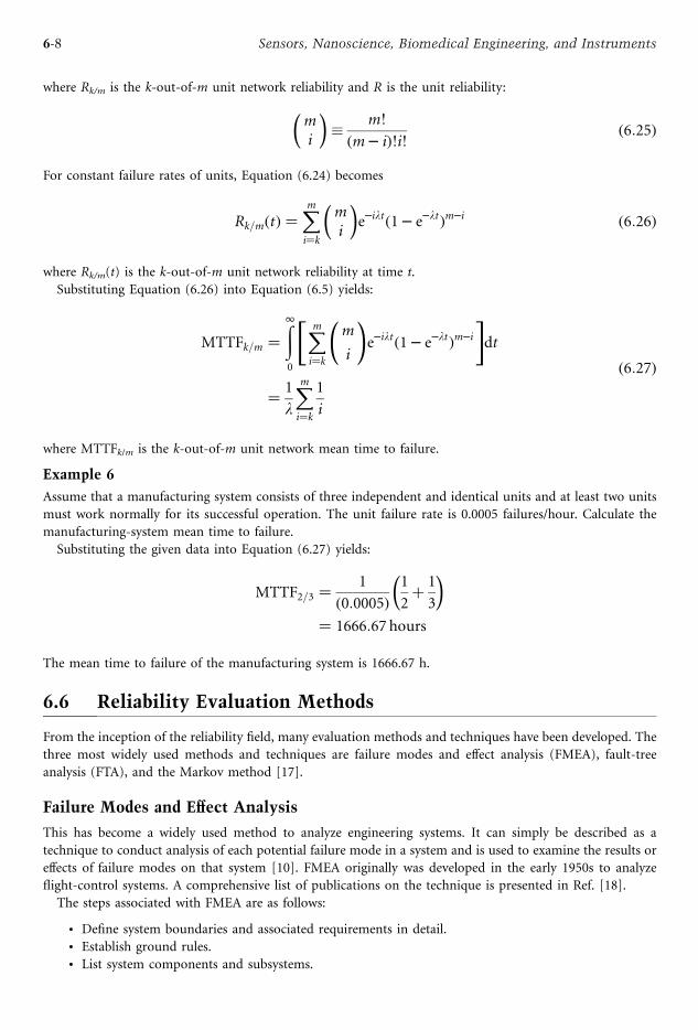
where Rk/m is the k-out-of-m unit network reliability and R is the unit reliability:
mi
m!
ðm iÞ!i! ð6:25Þ
For constant failure rates of units, Equation (6.24) becomes
Rk=mðtÞ ¼Xmi¼k
mi
e iltð1 e ltÞm i ð6:26Þ
where Rk/m(t) is the k-out-of-m unit network reliability at time t.
Substituting Equation (6.26) into Equation (6.5) yields:
MTTFk=m ¼Z10
Xmi¼k
m
i
!e iltð1 e ltÞm i
" #dt
¼ 1
l
Xmi¼k
1
i
ð6:27Þ
where MTTFk/m is the k-out-of-m unit network mean time to failure.
Example 6
Assume that a manufacturing system consists of three independent and identical units and at least two units
must work normally for its successful operation. The unit failure rate is 0.0005 failures/hour. Calculate the
manufacturing-system mean time to failure.
Substituting the given data into Equation (6.27) yields:
MTTF2=3 ¼ 1
ð0:0005Þ1
2þ 1
3
¼ 1666:67 hours
The mean time to failure of the manufacturing system is 1666.67 h.
6.6 Reliability Evaluation Methods
From the inception of the reliability field, many evaluation methods and techniques have been developed. The
three most widely used methods and techniques are failure modes and effect analysis (FMEA), fault-tree
analysis (FTA), and the Markov method [17].
Failure Modes and Effect Analysis
This has become a widely used method to analyze engineering systems. It can simply be described as a
technique to conduct analysis of each potential failure mode in a system and is used to examine the results or
effects of failure modes on that system [10]. FMEA originally was developed in the early 1950s to analyze
flight-control systems. A comprehensive list of publications on the technique is presented in Ref. [18].
The steps associated with FMEA are as follows:
. Define system boundaries and associated requirements in detail.
. Establish ground rules.
. List system components and subsystems.
6-8 Sensors, Nanoscience, Biomedical Engineering, and Instruments

. List important failure modes, describing and identifying the component in question.
. Assign failure rate/probability to each component failure mode.
. Document each failure mode effect on the subsystem/system/plant.
. Enter remarks for each failure mode.
. Review and identify critical failure modes and take corrective measures.
Assigning criticalities or priorities to failure-mode effects is known as failure modes, effects and criticality
analysis (FMECA). FMECA has some important characteristics:
. It is an upward approach that starts from the detailed level.
. By evaluating the failure effects of each component, the entire system is screened.
. It offers an effective approach to identify weak spots in system design, indicating areas for detailed
analysis or corrective measures.. It is useful to improve communication among design-interface personnel.
This approach is described in detail in Ref. [17].
Fault-Tree Analysis
This is another widely used method in the industrial sector to perform reliability analysis for engineering
systems. The method was developed in the early 1960s at the Bell Telephone Laboratories to analyze the
Minuteman launch control system. A comprehensive list of publications on the technique is presented in
Ref. [7]. Four basic symbols used to perform FTA are shown in Figure 6.4.
The following steps are used in performing FTA:
. Define the system and assumptions associated with the analysis.
. Identify the undesirable or top-fault event to be investigated.
. Thoroughly understand the system under study.
. Using fault-tree symbols, identify all the possible causes for the occurrence of the top event.
. Develop the fault tree to the lowest level required.
. Conduct an analysis of the completed fault tree.
. Identify corrective actions.
. Document the FTA and review corrective measures taken.
Example 7
A windowless room contains one switch and two light bulbs. The switch only can fail to close. Develop a fault
tree for the top event, ‘‘dark room.’’
(a)
Output fault
(b)
Output fault
(c)Input faults
(d)
Input faults
FIGURE 6.4 Fault tree basic symbols: (a) basic fault event, (b) resultant fault event, (c) OR gate, and (d) AND gate.
6-9Reliability Engineering
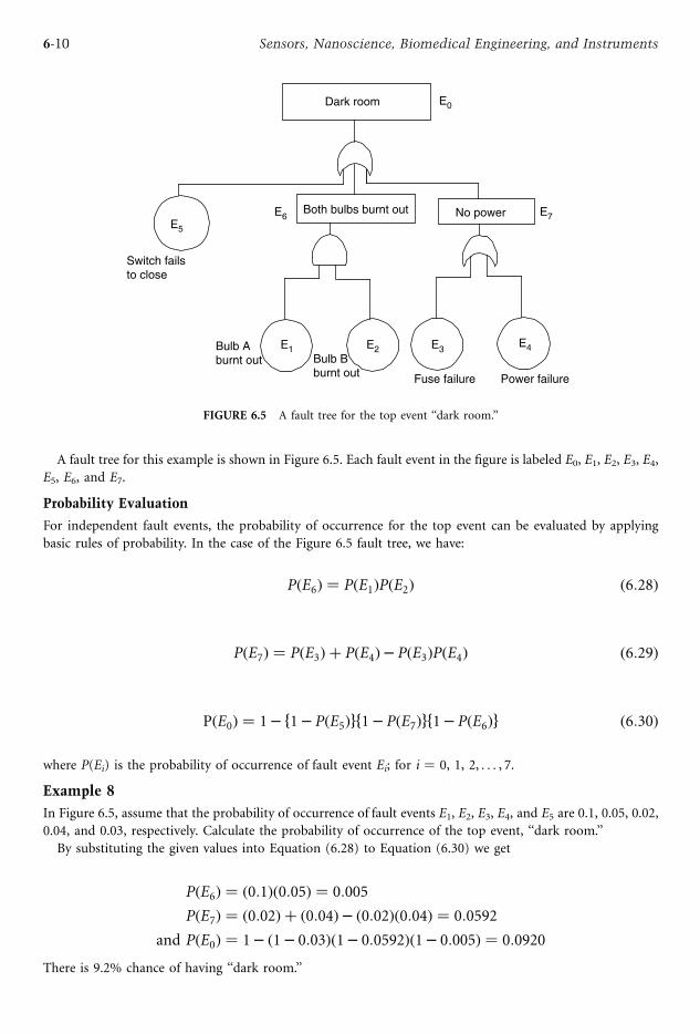
A fault tree for this example is shown in Figure 6.5. Each fault event in the figure is labeled E0, E1, E2, E3, E4,
E5, E6, and E7.
Probability Evaluation
For independent fault events, the probability of occurrence for the top event can be evaluated by applying
basic rules of probability. In the case of the Figure 6.5 fault tree, we have:
PðE6Þ ¼ PðE1ÞPðE2Þ ð6:28Þ
PðE7Þ ¼ PðE3Þ þ PðE4Þ PðE3ÞPðE4Þ ð6:29Þ
PðE0Þ ¼ 1 f1 PðE5Þgf1 PðE7Þgf1 PðE6Þg ð6:30Þ
where P(Ei) is the probability of occurrence of fault event Ei; for i ¼ 0, 1, 2, . . . , 7.
Example 8
In Figure 6.5, assume that the probability of occurrence of fault events E1, E2, E3, E4, and E5 are 0.1, 0.05, 0.02,
0.04, and 0.03, respectively. Calculate the probability of occurrence of the top event, ‘‘dark room.’’
By substituting the given values into Equation (6.28) to Equation (6.30) we get
PðE6Þ ¼ ð0:1Þð0:05Þ ¼ 0:005
PðE7Þ ¼ ð0:02Þ þ ð0:04Þ ð0:02Þð0:04Þ ¼ 0:0592
and PðE0Þ ¼ 1 ð1 0:03Þð1 0:0592Þð1 0:005Þ ¼ 0:0920
There is 9.2% chance of having ‘‘dark room.’’
Dark room
E5
E6
E2E1 E3E4
E7
E0
Switch failsto close
Both bulbs burnt out No power
Bulb Aburnt out Bulb B
burnt out Fuse failure Power failure
FIGURE 6.5 A fault tree for the top event ‘‘dark room.’’
6-10 Sensors, Nanoscience, Biomedical Engineering, and Instruments

Advantages and Disadvantages of FTA
As in the case of other evaluation methods, FTA has both advantages and disadvantages. Some advantages of
FTA are as follows:
. It provides insight into the system behavior.
. It easily can work with complex systems.
. It ferrets out failures deductively.
. It requires analysts that thoroughly understand the system under study.
. It offers a useful visibility tool to justify design changes and to conduct trade-off studies.
. It provides an option for performing either a qualitative or quantitative reliability analysis.
Similarly, some disadvantages of performing FTA are as follows:
. It can be costly and time-consuming.
. End results are difficult to check.
. It is difficult to manage a component’s partial failure states.
The Markov Method
This method, named after a Russian mathematician, is another frequently used method to perform a reliability
analysis for engineering systems. Like the others, it can work with repairable systems and systems with partial
failure states. The following assumptions are part of this approach:
. The transitional probability from one state to the other in the finite time interval Dt is given by lDt,where l is the failure or repair rate associated with Markov states.
. All occurrences are independent of each other.
. The probability of more than one transition occurrence in time interval Dt from one state [U8] to the
next state is small.
The following example demonstrates this method:
Example 9
A manufacturing system’s state-space diagram is shown in Figure 6.6. The manufacturing system either can be
in its operating state or its failed state. Appling the Markov method, develop expressions for the
manufacturing system’s reliability and unreliability if its failure rate is l. Numerals in the Figure 6.6 diagramdenote system states.
By applying the Markov method, we write the following two equations for the Figure 6.6 diagram:
P0ðt þ DtÞ ¼ P0ðtÞ½1 lDt ð6:31Þ
P1ðt þ DtÞ ¼ P1ðtÞ þ lDtP0ðtÞ ð6:32Þ
Manufacturingsystem
operating normally
0
Manufacturingsystem failed
1
λ
FIGURE 6.6 Manufacturing system state-space diagram.
6-11Reliability Engineering
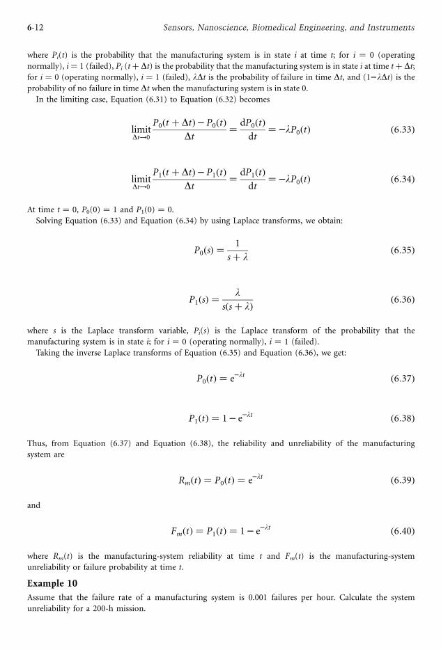
where Pi(t) is the probability that the manufacturing system is in state i at time t; for i ¼ 0 (operating
normally), i¼ 1 (failed), Pi (tþ Dt) is the probability that the manufacturing system is in state i at time tþ Dt;for i ¼ 0 (operating normally), i ¼ 1 (failed), lDt is the probability of failure in time Dt, and (1 lDt) is theprobability of no failure in time Dt when the manufacturing system is in state 0.
In the limiting case, Equation (6.31) to Equation (6.32) becomes
limitDt!0
P0ðt þ DtÞ P0ðtÞDt
¼ dP0ðtÞdt
¼ lP0ðtÞ ð6:33Þ
limitDt!0
P1ðt þ DtÞ P1ðtÞDt
¼ dP1ðtÞdt
¼ lP0ðtÞ ð6:34Þ
At time t ¼ 0, P0(0) ¼ 1 and P1(0) ¼ 0.
Solving Equation (6.33) and Equation (6.34) by using Laplace transforms, we obtain:
P0ðsÞ ¼ 1
sþ lð6:35Þ
P1ðsÞ ¼ lsðsþ lÞ ð6:36Þ
where s is the Laplace transform variable, Pi(s) is the Laplace transform of the probability that the
manufacturing system is in state i; for i ¼ 0 (operating normally), i ¼ 1 (failed).
Taking the inverse Laplace transforms of Equation (6.35) and Equation (6.36), we get:
P0ðtÞ ¼ e lt ð6:37Þ
P1ðtÞ ¼ 1 e lt ð6:38Þ
Thus, from Equation (6.37) and Equation (6.38), the reliability and unreliability of the manufacturing
system are
RmðtÞ ¼ P0ðtÞ ¼ e lt ð6:39Þ
and
FmðtÞ ¼ P1ðtÞ ¼ 1 e lt ð6:40Þ
where Rm(t) is the manufacturing-system reliability at time t and Fm(t) is the manufacturing-system
unreliability or failure probability at time t.
Example 10
Assume that the failure rate of a manufacturing system is 0.001 failures per hour. Calculate the system
unreliability for a 200-h mission.
6-12 Sensors, Nanoscience, Biomedical Engineering, and Instruments

By inserting the given data into Equation (6.40), we have:
Fmð200Þ ¼ 1 e ð0:001Þð200Þ
¼ 0:1813
There is a 18.13% chance that the manufacturing system will fail during the specified period.
6.7 Human Reliability
As human links connect numerous engineering systems, reliability is an important factor in the successful
operation of such systems. In the late 1950s, Williams [19] recognized the problem of human reliability in
engineering systems and wrote that the reliability of the human element must be incorporated. Various studies
subsequently have indicated that at least 10% of system failures are caused by human error [17,20].
The first book on human reliability appeared in 1986 [21]. Today, many other texts are available on the
subject. A comprehensive list of publications on human reliability is presented in Ref. [7].
Classification and Causes of Human Errors
Human errors can be classified as follows [22]:
. Design errors
. Operator errors
. Maintenance errors
. Fabrication errors
. Inspection errors
. Handling errors
. Contributory errors
Human errors can be caused by a poor work environment (inadequate lighting, crowded workspaces, high
noise levels), inadequate or poorly worded equipment operating and maintenance procedures, poor
equipment design, wrong or inadequate work tools, complex tasks, poor work layout, low skill levels or
inadequate worker training and unmotivated employees [21–23].
Human Reliability Measures
The following two equations can estimate human reliability:
HR ¼ 1E
nð6:41Þ
and
RhðtÞ ¼ e
Rt0
lhðtÞdt ð6:42Þ
where HR is human reliability, n is the total number of times the certain task was performed, E is the number
of times the task was performed incorrectly, Rh(t) is the human reliability at time t, and lh(t) is the time-dependent human error rate.
6-13Reliability Engineering

Equation (6.42) is used to compute the reliability of time-continuous tasks such as scope monitoring,
aircraft maneuvering, and operating an automobile. The following two examples demonstrate the application
of Equation (6.41) and Equation (6.42).
Example 11
A person performed a task 200 times. It was performed incorrectly 15 times. Calculate the human reliability.
The specified data in Equation (6.41) yields:
HR ¼ 115
200
¼ 0:9250
In this case, the value of human reliability is 92.50%.
Example 12
A person performed a time-continuous task, and the error rate was 0.004 errors per hour. Calculate the
person’s reliability over an 8-h period.
Substituting the given data into Equation (6.42), we get:
Rhð8Þ ¼ e
R80
ð0:004Þdt
¼ e ð0:004Þð8Þ
¼ 0:9685
The person’s reliability is 96.85%.
Modeling Human Operation in a Fluctuating Environment
This model represents situations where the human operator performs a time-continuous task under
alternating environments, both normal and abnormal. Two examples of such situations are operating a vehicle
in normal and heavy traffic and piloting an aircraft in normal and extreme weather. The operator can make
mistakes in both normal and abnormal conditions, but their occurrence rates could differ [24].
This model can calculate operator reliability and mean time to human error. The model state-space diagram
is shown in Figure 6.7. The numerals in Figure 6.7 boxes and circles denote system states. The following
symbols were used to develop equations for the model: Pi(t) is the probability of the human operator being in
state i at time t; for i ¼ 0, 1, 2, 3, l1 is the human-operator error rate from state 0, l2 is the human-operatorerror rate from state 2, a is the transition rate from a normal to an abnormal state, and b is the transition ratefrom an abnormal to a normal state.
Applying the Markov method, we get the following equations for the Figure 6.7 state-space diagram [24]:
dP0ðtÞdt
þ ðl1 þ aÞP0ðtÞ ¼ P2ðtÞ ¼ P2ðtÞb ð6:43Þ
dP1ðtÞdt
¼ P0ðtÞl1 ð6:44Þ
6-14 Sensors, Nanoscience, Biomedical Engineering, and Instruments

dP2ðtÞdt
þ ðl2 þ bÞP2ðtÞ ¼ P0ðtÞa ð6:45Þ
dP3ðtÞdt
¼ P2ðtÞl2 ð6:46Þ
At time t ¼ 0, P0(0) ¼ 1, and P1(0) ¼ P2(0) ¼ P3(0) ¼ 0.
Solving the above equations, we get the following expression for the human-operator reliability:
RhðtÞ ¼ P0ðtÞ þ P2ðtÞ¼ ðx2 x1Þ 1½ðx2 þ l2 þ b ex2t ðx1 þ l2 þ bÞex1t þ aðex2t ex1tÞ ð6:47Þ
where
x1 ¼ b1 þffiffiffiffiffiffiffiffiffiffib21 4b2
p2
ð6:48Þ
x2 ¼ b1ffiffiffiffiffiffiffiffiffiffib21 4b2
p2
ð6:49Þ
b1 ¼ l1 þ l2 þ aþ b ð6:50Þ
b2 ¼ l1ðl2 þ bÞ þ al2 ð6:51Þ
Operatorperforming tasksuccessfully innormalenvironment
Operatorperforming tasksuccessfully inabnormalenvironment
0
System faileddue to humanerror in normalenvironment
System faileddue to humanerror inabnormalenvironment
1
2 3
βα
λ1
λ2
FIGURE 6.7 State-space diagram for the human operator under fluctuating stress environment.
6-15Reliability Engineering

By integrating Equation (6.47) over the time interval 0 to 1, we get:
MTTHOE ¼Z10
RhðtÞdt
¼ ðl2 þ aþ bÞ=b2ð6:52Þ
where MTTHOE is the mean time to human-operator error.
6.8 Robot Reliability
Though the idea of a functional robot can be traced to the writings of Aristotle in the fourth century B.C., the
programmable device developed by George Devol in 1954 is regarded as the first industrial robot [25,26].
Today, robots are an important component of manufacturing systems.
In the early 1980s, robot reliability began to attract serious attention. In 1987, a comprehensive list of
publications was first published on robot reliability and safety [27]. In 1991, a book titled Robot Reliability and
Safety covered the subject in considerable depth [28]. Since then, many publications on robot reliability have
been published.
Robot Failure Classifications and Causes
There are various failure types associated with robots and they can be classified into four categories [29,30]:
1. Random component failures
2. Systematic hardware faults
3. Software faults
4. Human errors
Random component failures occur unpredictably during the useful life of a robot. Reasons for their
occurrence include low safety factors, undetectable defects, and unavoidable failures. Systematic hardware
faults are the result of unrevealed mechanisms in the robot’s design.
Software faults in robots occur due to embedded software or the controlling and application software.
As with any other engineering system, human error also can occur during design, manufacturing, testing,
operation, and maintenance of a robot.
There are various causes for robot failures. Frequent ones are servo value malfunctions, oil-pressure valve
problems, circuit board problems, and human error. Nonetheless, some past studies [31,32] have indicated
that robot problems occur in the following order:
. Control-system problems
. Jig and other tool incompatibility
. Robot body problems
. Programming and operation errors
. Welding-gun problems and problems with other tooling parts
. Deterioration and precision deficiency
. Runaway
. Other problems
Robot Reliability Measures
Several parameters measure robot reliability, including mean time to robot failure (MTRF), reliability, and
mean time to robot-related problems (MTRP). Each is presented below.
6-16 Sensors, Nanoscience, Biomedical Engineering, and Instruments

Mean Time to Robot Failure (MTRF)
This can be defined in two ways:
MTRF ¼ ðRPH DTDRFÞ=N ð6:53Þ
where N is the total number of robot failures; RPH is the robot production time, expressed in hours; and
DTDRF is downtime due to robot failures, expressed in hours, or:
MTRF ¼Z10
RbðtÞdt ð6:54Þ
where Rb(t) is the robot reliability at time t.
Example 13
Assume that total number of production hours for a robot system was 6000 h, with downtime due to robot
failure of 200 h. If there were 10 robot failures during this period, calculate the robot mean time to failure.
By inserting the given values into Equation (6.53), we obtain:
MTRF ¼ ð6; 000 200Þ=10¼ 580 hours
On average, the robot failed after every 580 h of operation.
Robot Reliability
This is defined by:
RrðtÞ ¼ expZt0
lrðtÞdt264
375 ð6:55Þ
where Rr(t) is the robot reliability at time t and lr(t) is the robot hazard rate or time-dependent failure rate.
Example 14
A robot failure rate is 0.0005 failures per hour. Calculate robot reliability during a 200-h mission.
Substituting the above data into Equation (6.55) yields:
Rrð200Þ ¼ expZ2000
ð0:0005Þdt264
375 ¼ e ð0:0005Þ ð200Þ ¼ 0:9048
There is a 90.48% chance that the robot will not fail during the 200-h mission.
Mean Time to Robot-Related Problems (MTRP)
This is defined by
MTRP ¼ RPH DTDRP
Mð6:56Þ
where M is the total number of robot-related problems and DTDRP is downtime due to robot-related
problems, expressed in hours.
6-17Reliability Engineering

Example 15
The total number of production hours of an industrial robot was 8000 h, including downtime due to robot-
related problems of 500 h. In addition, there were 20 robot-related problems. Calculate the mean time to
robot-related problems.
Using the data in Equation (6.56), we get:
MTRP ¼ 8;000 500
20¼ 375 hours
The mean time to robot-related problems is 375 h.
References
1. B.S. Dhillon and C. Singh, Engineering Reliability: New Techniques and Applications, New York:
Wiley, 1981.
2. Reliability and Maintainability Guideline for Manufacturing Machinery and Equipment, Warrendale,
PA: Society of Automotive Engineers, Inc., M-110.2, 1999.
3. AGREE Report, Reliability of Military Electronic Equipment, Washington, D.C.: Department of Defense,
1957.
4. MIL-R-25717 (USAF), Reliability Assurance Program for Electronic Equipment, Washington, D.C.:
Department of Defense, 1957.
5. W.Weibull, ‘‘A statistical distribution function of wide applicability,’’ J. Appl. Mech., vol. 47, pp. 293–297,
1951.
6. K. Henney, Ed., Reliability Factors for Ground Electronic Equipment, New York: McGraw-Hill, 1956.
7. B.S. Dhillon, Reliability and Quality Control: Bibliography on General and Specialized Areas, Gloucester,
ON: Beta Publishers, 1992.
8. B.S. Dhillon, Reliability Engineering Applications: Bibliography on Important Application Areas,
Gloucester, ON: Beta Publishers, 1992.
9. J.J. Naresky, ‘‘Reliability definitions,’’ IEEE Trans. Reliab., vol. 19, pp. 198–200, 1970.
10. T.P. Omdahl, Ed., Reliability, Availability, and Maintainability (RAM) Dictionary, Milwaukee, WI:
ASQC Quality Press, 1988.
11. T. McKenna and R. Oliverson, Glossary of Reliability and Maintenance, Houston, TX: Gulf Publishing
Company, 1997.
12. B.S. Dhillon, Reliability Engineering in Systems Design and Operation, New York: Van Nostrand
Reinhold Company, 1983.
13. W.H. Von Alven, Ed., Reliability Engineering, Englewood Cliffs, NJ: Prentice-Hall, 1964.
14. B.S. Dhillon, Mechanical Reliability: Theory, Models and Applications, Washington, D.C.: American
Institute of Aeronautics and Astronautics, 1988.
15. W. Grant Ireson and C.F. Coombs, Eds., Handbook of Reliability Engineering and Management,
New York: McGraw-Hill, 1988.
16. B.S. Dhillon, ‘‘A hazard rate model,’’ IEEE Trans. Reliab., vol. 29, p. 150, 1979.
17. B.S. Dhillon, Design Reliability: Fundamentals and Applications, Boca Raton, FL: CRC Press, 1999.
18. B.S. Dhillon, ‘‘Failure modes and effect analysis: bibliography,’’ Microelectron. Reliab., vol. 32,
pp. 729–731, 1992.
19. H.L. Williams, ‘‘Reliability evaluation of the human component in man-machine systems,’’ Electr.
Manuf., pp. 78–82, 1958 (April).
20. E.W. Hagen, Ed., ‘‘Human reliability analysis,’’ Nucl. Safety, vol. 17, pp. 315–326, 1976.
21. B.S. Dhillon, Human Reliability with Human Factors, New York: Pergamon Press, 1986.
22. D. Meister, ‘‘The problem of human-initiated failures,’’ Proc. Eighth Natl. Symp. Reliab. Qual. Contr.,
pp. 234–239, 1962.
6-18 Sensors, Nanoscience, Biomedical Engineering, and Instruments

23. J.I. Cooper, ‘‘Human-initiated failures and man-function reporting,’’ IRE Trans. Human Factors, vol. 10,
pp. 104–109, 1961.
24. B.S. Dhillon, ‘‘Stochastic models for predicting human reliability,’’ Microelectron. Reliab., vol. 22,
pp. 491–496, 1982.
25. E. Heer, ‘‘Robots in modern industry,’’ in Recent Advances in Robotics, G. Beni and S. Hackwood, Eds.,
New York: Wiley, pp. 11–36, 1985.
26. M.I. Zeldman, What Every Engineer Should Know about Robots, New York: Marcel Dekker, 1984.
27. B.S. Dhillon, ‘‘On robot reliability and safety,’’ Microelectron. Reliab., vol. 27, pp. 105–118, 1987.
28. B.S. Dhillon, Robot Reliability and Safety, New York: Springer, 1991.
29. K. Khodabandehloo, F. Duggan, and T.F. Husband, ‘‘Reliability of industrial robots: a safety
viewpoint,’’ Proc. 7th Br. Robot Assoc. Annu. Conf., pp. 233–242, 1984.
30. K. Khodabandehloo, F. Duggan, and T.F. Husband, ‘‘Reliability assessment of industrial robots,’’
Proc. 14th Int. Symp. Ind. Robots, pp. 209–220, 1984.
31. K. Sato, ‘‘Case study of maintenance of spot-welding robots,’’ Plant Maint., pp. 14–28, 1982.
32. N. Sugimoto and K. Kawaguchi, ‘‘Fault tree analysis of hazards created by robots,’’ Proc. 13th Int. Symp.
Ind. Robots, pp. 9.13–9.28, 1983.
6-19Reliability Engineering


IIBiomedicalSystems
7 Bioelectricity J.A. White, A.D. Dorval II, L.A. Geddes, R.C. Barr,B.K. Slaten, F. Barnes, D.R. Martinez, R.A. Bond, M.M. Vai .................................................... 7-1Neuroelectric Principles * Bioelectric Events * Biological Effects and ElectromagneticFields * Embedded Signal Processing
8 Biomedical Sensors M.R. Neuman .......................................................................................... 8-1Introduction * Physical Sensors * Chemical Sensors * Bioanalytical Sensors * Applications
9 Bioelectronics and Instruments J.D. Bronzino, E.J. Berbari................................................. 9-1The Electro-encephalogram * The Electrocardiograph
10 Tomography M.D. Fox ............................................................................................................ 10-1Computerized Tomography * Positron Emission Tomography * Single Photon EmissionComputed Tomography * Magnetic Resonance Imaging * Imaging
II-1


7Bioelectricity
John A. WhiteBoston University
Alan D. Dorval IIBoston University
L.A. GeddesPurdue University
R.C. BarrDuke University
Bonnie Keillor SlatenUniversity of Colorado
Frank BarnesUniversity of Colorado
David R. MartinezMIT Lincoln Laboratory
Robert A. BondMIT Lincoln Laboratory
M. Michael VaiMIT Lincoln Laboratory
7.1 Neuroelectric Principles ......................................................... 7-1Introduction * Electrochemical Potential * Action Potentials *
Synaptic Transmission * Dynamic Clamp * Models of
Extracellular Stimulation * Application: Deep Brain Stimulation
7.2 Bioelectric Events ............................................................... 7-13Origin of Bioelectricity * Law of Stimulation * Recording Action
Potentials * The Electrocardiogram (ECG) * Electromyography
(EMG) * Electro-encephalography (EEG) * Magnetic (Eddy-Current)
Stimulation * Summary and Conclusion
7.3 Biological Effects and Electromagnetic Fields .......................... 7-33Introduction * Biological Effects of Electric Shock * Will the 120-V
Common Household Voltage Produce a Dangerous Shock?
It Depends! * Other Adverse Effects of Electricity * Biological
Effects of Low Level, Time-Varying Electromagnetic Fields (EMF) from
Power Lines * Exposures * Epidemiological Studies * Animal Studies *
Cellular Studies * EMF from Cell Phones and Base Stations *
Exposures * Epidemiological Studies * Animal Studies (In vivo) *
Cellular Studies * Standards and Guidelines * Conclusion
7.4 Embedded Signal Processing ................................................ 7-55Introduction * Generic Embedded Signal Processing Architecture *
Embedded Digital Signal Processor (DSP) * Software: Run-Time
and Development Environment * Programmable DSP Technology
Trends * Application-Specific Hardware * Summary
7.1 Neuroelectric Principles
John A. White and Alan D. Dorval II
Introduction
In the nervous system, signaling on fast time scales (10 4 to 10 1 sec) is electrical in nature. Neurons (nerve
cells), the basic functional units of the nervous system, continually expend energy to maintain electrochemical
gradients across their cell membranes. In response to an appropriate stimulus, neurons allow ions (mostly
Naþ and Kþ) to run down their potential energy gradients. This charge movement leads to a brief, 100-mVchange in membrane potential, known as the action potential. Action potentials are typically generated near
the cell body and propagate down specialized processes (axons) to target nerve and muscle cells. Neuroelectric
activity is studied by measuring electrical events both intracellularly and extracellularly. Recent technical
advances allow basic researchers to mimic ion channels in living neuronal membranes. Applied scientists have
used electrical stimulation of the nervous system to great clinical effect, but the specific mechanisms being
exploited are still an object of active study.
7-1
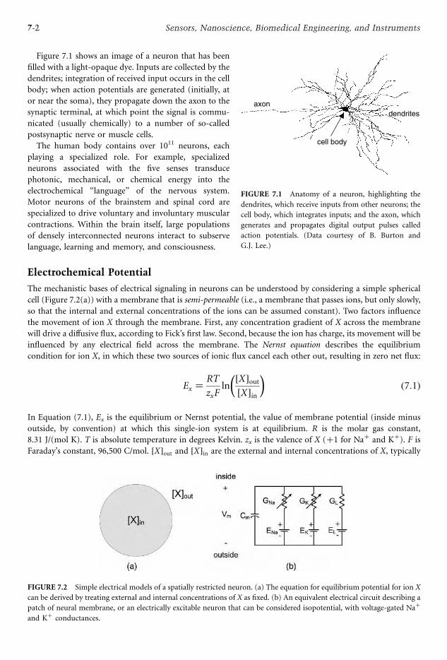
Figure 7.1 shows an image of a neuron that has been
filled with a light-opaque dye. Inputs are collected by the
dendrites; integration of received input occurs in the cell
body; when action potentials are generated (initially, at
or near the soma), they propagate down the axon to the
synaptic terminal, at which point the signal is commu-
nicated (usually chemically) to a number of so-called
postsynaptic nerve or muscle cells.
The human body contains over 1011 neurons, each
playing a specialized role. For example, specialized
neurons associated with the five senses transduce
photonic, mechanical, or chemical energy into the
electrochemical ‘‘language’’ of the nervous system.
Motor neurons of the brainstem and spinal cord are
specialized to drive voluntary and involuntary muscular
contractions. Within the brain itself, large populations
of densely interconnected neurons interact to subserve
language, learning and memory, and consciousness.
Electrochemical Potential
The mechanistic bases of electrical signaling in neurons can be understood by considering a simple spherical
cell (Figure 7.2(a)) with a membrane that is semi-permeable (i.e., a membrane that passes ions, but only slowly,
so that the internal and external concentrations of the ions can be assumed constant). Two factors influence
the movement of ion X through the membrane. First, any concentration gradient of X across the membrane
will drive a diffusive flux, according to Fick’s first law. Second, because the ion has charge, its movement will be
influenced by any electrical field across the membrane. The Nernst equation describes the equilibrium
condition for ion X, in which these two sources of ionic flux cancel each other out, resulting in zero net flux:
Ex ¼ RT
zxFln
½X out
½X in
ð7:1Þ
In Equation (7.1), Ex is the equilibrium or Nernst potential, the value of membrane potential (inside minus
outside, by convention) at which this single-ion system is at equilibrium. R is the molar gas constant,
8.31 J/(mol K). T is absolute temperature in degrees Kelvin. zx is the valence of X (þ1 for Naþ and Kþ). F isFaraday’s constant, 96,500 C/mol. ½X out and ½X in are the external and internal concentrations of X, typically
FIGURE 7.2 Simple electrical models of a spatially restricted neuron. (a) The equation for equilibrium potential for ion X
can be derived by treating external and internal concentrations of X as fixed. (b) An equivalent electrical circuit describing a
patch of neural membrane, or an electrically excitable neuron that can be considered isopotential, with voltage-gated Naþ
and Kþ conductances.
axondendrites
cell body
FIGURE 7.1 Anatomy of a neuron, highlighting the
dendrites, which receive inputs from other neurons; the
cell body, which integrates inputs; and the axon, which
generates and propagates digital output pulses called
action potentials. (Data courtesy of B. Burton and
G.J. Lee.)
7-2 Sensors, Nanoscience, Biomedical Engineering, and Instruments

expressed in mM. It is often more convenient to convert the Nernst equation to log10, and to assume a value of
temperature. At 37–C, the Nernst equation reduces to
Ex <61
zxlog10
½X out
½X in
ð7:2Þ
where Ex has units of mV.
As noted above, Naþ and Kþ are crucial for neuroelectric signaling. Inmammalian nerve andmuscle cells, theexternal concentration of Naþ is approximately an order of magnitude greater than the internal concentration,leading to an Naþ Nernst potential ENa < þ60 mV. In contrast, the internal concentration of Kþ is more thanan order of magnitude greater than the external concentration, giving a Kþ Nernst potential EKv < 80 mV.
The disparate values of ENa and EK imply that these two ions cannot be in equilibrium simultaneously. In
fact, neither Naþ nor Kþ is typically in equilibrium. The simple electrical model shown in Figure 7.2(b) is
commonly used to describe small patches of neuronal membrane that are permeant to both Naþ and Kþ
(along with other ions). In this model, Cm represents membrane capacitance, generated by the relatively
poorly conducting cell membrane between the highly conductive intracellular and extracellular fluids. GNa and
GK represent membrane conductances that specifically pass Naþ and Kþ, respectively. Note that these
conductances are, in general, nonlinear. GL represents the so-called ‘‘leak’’ conductance. This conductance
represents the flow of multiple ions through linear membrane conductances. The battery EL represents the
Thevenin equivalent combination of the Nernst potentials of all of the ions flowing through the linear
conductance. In the steady state, membrane potential Vm is given by the equation:
Vm ¼ GNaENa þ GKEK þ GLELGNa þ GK þ GL
ð7:3Þ
This simple equation has the important implication that Vm is bounded between ENa (þ60 mV) and EK( 80 mV). (EL lies between these bounds.) Thus, neurons have an operating range of slightly more than
100 mV. Under steady-state conditions, GK is typically significantly larger than GNa or GL, consistent with
typical resting values of Vm < 65 mV.
Because both Naþ and Kþ are out of equilibrium at rest, there is a constant inward trickle of Naþ (because
Vm , ENa) and outward trickle of Kþ (because Vm . EK). Over time-scales of minutes to hours, this trickle
would be sufficient to ‘‘run down’’ the concentration gradients in Naþ and Kþ, thus causing ENa and EK toapproach zero. Nerve cells expend energy to continually pump Naþ out and Kþ in, thus maintaining nearly
constant values of ENa and EK throughout life.
Action Potentials
Neurons make use of their nonequilibrium conditions for purposes of signaling. Figure 7.3 shows results from
a hypothetical experiment in which an electrode has been inserted into a neuron. Parameters match those
from the ‘‘giant axon’’ of the squid, in which the mechanisms underlying action potentials were first elucidated
(see below). The left panels show responses of this gedanken neuron to a square pulse of current
(duration ¼ 1 msec, amplitude ¼ 5 mA/cm2, onset at t ¼ 0 msec). This stimulus induces only a small
deflection in membrane potential. Both GNa and GK remain very near their resting values. For stimuli of this
size, the cell is well approximated by the circuit of Figure 7.2(b), with ohmic conductances.
The situation changes dramatically for larger stimuli (Figure 7.3, right panels). Such stimuli induce a voltage
deflection with amplitude roughly 100 mV. This is the action potential. To a first approximation, the action
potential is all-or-nothing; large stimuli generate a stereotypical action potential like that in the upper-right
panel of Figure 7.3, whereas weak stimuli generate no action potential at all. For a fixed duration of the current
pulse, there is a sharply defined threshold for action potential generation.
The lower-right panel of Figure 7.3 gives insight into the mechanisms underlying the action potential. The
sharp rise in Vm near t¼ 1 msec, often referred to as the depolarizing phase of the action potential, is driven by
7-3Bioelectricity
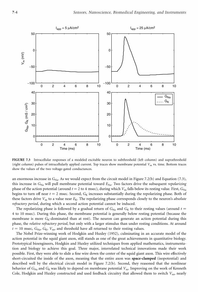
an enormous increase in GNa. As we would expect from the circuit model in Figure 7.2(b) and Equation (7.3),
this increase in GNa will pull membrane potential toward ENa. Two factors drive the subsequent repolarizing
phase of the action potential (around t ¼ 2 to 4 msec), during which Vm falls below its resting value. First, GNabegins to turn off near t ¼ 2 msec. Second, GK increases substantially during the repolarizing phase. Both of
these factors drive Vm to a value near EK. The repolarizing phase corresponds closely to the neuron’s absolute
refractory period, during which a second action potential cannot be induced.
The repolarizing phase is followed by a gradual return of GNa and GK to their resting values (around t ¼4 to 10 msec). During this phase, the membrane potential is generally below resting potential (because the
membrane is more GK-dominated than at rest). The neuron can generate an action potential during this
phase, the relative refractory period, but only with a larger stimulus than under resting conditions. At around
t ¼ 10 msec, GNa, GK, Vm, and threshold have all returned to their resting values.
The Nobel Prize-winning work of Hodgkin and Huxley (1952), culminating in an accurate model of the
action potential in the squid giant axon, still stands as one of the great achievements in quantitative biology.
Prototypical bioengineers, Hodgkin and Huxley utilized techniques from applied mathematics, instrumenta-
tion and biology to achieve this goal. Three major, interrelated technical innovations made their work
possible. First, they were able to slide a fine wire down the center of the squid giant axon. This wire effectively
short-circuited the inside of the axon, meaning that the entire axon was space-clamped (isopotential) and
described well by the electrical circuit model in Figure 7.2(b). Second, they reasoned that the nonlinear
behavior of GNa and GK was likely to depend on membrane potential Vm. Improving on the work of Kenneth
Cole, Hodgkin and Huxley constructed and used feedback circuitry that allowed them to switch Vm, nearly
0 2 4 6 8 10−100
−50
0
50
Vm
(mV
)
0 2 4 6 8 10
0
10
20
30
40
Time (ms)
GN
a,G
K(m
S/c
m2 )
0 2 4 6 8 10−100
−50
0
50
0 2 4 6 8 10
0
10
20
30
40
Time (ms)
GNa
GK
Iapp = 5 μA/cm2 Iapp = 25 μA/cm2
FIGURE 7.3 Intracellular responses of a modeled excitable neuron to subthreshold (left column) and suprathreshold
(right column) pulses of intracellularly applied current. Top traces show membrane potential Vm vs. time. Bottom traces
show the values of the two voltage-gated conductances.
7-4 Sensors, Nanoscience, Biomedical Engineering, and Instruments
instantaneously, from one constant value to another, and measure the resulting current fluxes through GNaand GK. The voltage-clamp technique remains one of the most valuable tools used by cellular
electrophysiologists. Third, Hodgkin and Huxley had the mathematical prowess to develop a relatively
simple set of four nonlinear differential equations that could be parameterized simply using voltage-clamp
data, and solved numerically to describe the action potential in the space-clamped axon. The full Hodgkin–
Huxley equations are described elsewhere (e.g., Weiss, 1996; White, 2002). The first of the four equations is
simply Kirchoff ’s current law applied to the circuit of Figure 7.2(b):
CmdVmdt
¼ GNaðVm; tÞ½Vm ENa GKðVm; tÞ½Vm EK GL½Vm EL ð7:4Þ
The second and third Hodgkin–Huxley equations (not shown) describe the processes by which GNa activates
(i.e., turns on to generate the depolarizing phase of the action potential) and inactivates (i.e., turns off during
the repolarizing phase of the action potential). Both processes depend nonlinearly on membrane potential Vm.
The fourth Hodgkin–Huxley equation describes Vm-dependent activation of GK.
Two features of the Hodgkin–Huxley model are crucial to account for the action potential:
1. GNa rapidly activates in response to depolarization of the membrane (i.e., positive excursions of Vm). This
property implies that GNa, once activated, is prone to destabilization via positive feedback: a small
depolarization partially activates GNa, which in turn further depolarizes the membrane, further activating
GNa, an so on. This destabilizing positive feedback gives rise to the depolarizing phase of the action
potential.
2. In response to depolarization, GNa eventually inactivates and GK activates, but these processes are an
order of magnitude slower than the activation of GNa. Both of these processes contribute to the
repolarizing phase of the action potential. Once the action potential is complete, these processes return to
their resting values over the course of several milliseconds. During the repolarizing phase, and
immediately afterward, GNa is nearly fully inactivated. Thus, the positive feedback mechanism cannot be
triggered, and the membrane is absolutely refractory. After the absolute refractory period comes the
relative refractory period, during which GNa is still partially inactivated and GK is partially activated.
Consequently, a larger depolarization than normal is required to trigger an action potential.
The greatest achievement of Hodgkin and Huxley was that their equations, parameterized under voltage-
and space-clamped conditions, accurately described the details of propagation of the action potential when
these conditions were relaxed. In simple bare axons (e.g., squid giant axon and small axons of the human
nervous system), called unmyelinated axons, the action potential propagates simply because the ‘‘spiking’’
region of the axon depolarizes adjacent regions, causing those regions to spike as well. In the wake of the
propagating action potential lies a region of refractory (unexcitable) membrane. Mathematically, this situation
is described by a nonlinear partial differential equation, the nonlinear cable equation (Hodgkin and Huxley,
1952; Weiss, 1996):
1
2paðri þ roÞq2Vmqz2
¼ CmqVmqt
þ GNaðVm; tÞ½Vm ENa þ GKðVm; tÞ½Vm EK
þ GL½Vm EL ð7:5Þ
where a is the axonal radius; ri and ro are the internal and external resistances per unit length of axon,
respectively; and z is distance along the cylindrical axon. Note that Vm in Equation (7.5) is a function of both z
and t.
Large axons of the human body are usually myelinated: most of the axon is covered by an insulating sheath,
with periodic patches of bare axon called nodes of Ranvier. In myelinated axons, nonlinear ionic fluxes occur
only at the nodes. Excitation of one node is sufficient to rapidly depolarize and excite adjacent nodes. The
resulting ‘‘saltatory’’ conduction of the action potential is faster, for large axons, than the continuous
7-5Bioelectricity
conduction seen in unmyelinated axons (Weiss, 1996). A number of serious neurological conditions, including
multiple sclerosis and chronic inflammatory demyelinating polyneuropathy (CIDP), involve disruption of
axonal myelination.
More recent work on action potentials has revealed the molecular mechanisms underlying voltage-gated
membrane conductances. Most notably, two Nobel Prizes have been granted in this area. Sakmann and Neher
won the 1991 Nobel Prize in Physiology or Medicine for their conclusive, direct recordings of ion flow through
single ion channels (see Sakmann and Neher, 1995). To a great degree, the problems solved by Sakmann and
Neher were engineering problems. In particular, they took a number of steps to dramatically improve the
signal-to-noise ratio of their recordings, eventually managing to obtain clean recordings of the single-channel
currents (on the order of pA). MacKinnon won the 2003 Nobel Prize in Chemistry for obtaining and
interpreting high-resolution x-ray-crystallographic images of voltage-gated ion channels. Using these images,
MacKinnon explained the mechanism by which an individual ion channel can pass Kþ but exclude Naþ, an ionwith very similar chemical properties but much different effects on membrane potential (Doyle et al., 1998).
Synaptic Transmission
Action potentials generated in an individual neuron influence each other via either chemical or electrical
synapses. In chemical synapses, the axonal action potential triggers release of small vesicles of chemically active
substances called neurotransmitters, which diffuse across the small synaptic cleft to an adjacent neuron.
Chemically gated ion channels respond to these neurotransmitters by opening or closing, leading to effects that
can be understood electrically using simple elaborations of Figure 7.2(b). Chemical neurotransmitters can also
trigger a wide-ranging set of biochemical effects that operate on a slower time scale than the direct electrical
effects.
Electrical synapses, formed by so-called gap junctions between physically adjacent neurons, are perhaps less
prevalent in the nervous system than in the heart, but they still serve as important lines of communication
between neurons. From an electrical perspective, electrical synapses can be modeled as resistors connecting
multiple compartments of the form seen in Figure 7.2(b). Linear (ohmic) electrical synapses seem to be more
prevalent than nonlinear electrical synapses, but both kinds have been observed.
Dynamic Clamp
For decades, cellular electrophysiologists have relied upon two intracellular recording techniques: current-
clamp recordings (e.g., Figure 7.3), in which electrical current is passed into the cell and resulting changes in
Vm are observed; and voltage-clamp recordings, in which Vm is manipulated and the resulting membrane
currents are measured. More recently, a third recording technique, termed the dynamic clamp or conductance
clamp technique, has been developed (Prinz et al., 2004). The dynamic clamp allows the neurophysiologist to
introduce virtual membrane conductances into the neuronal membrane. Thus, the user has the newfound
ability to introduce realistic virtual chemical synaptic inputs into the neuron; to couple two recorded neurons
via virtual electrical and/or chemical synapses, or to construct hybrid neuronal networks, consisting of
biological and artificial neurons that are coupled in realistic, user-defined ways.
The dynamic clamp method is inherently more complex than the current clamp or voltage clamp
techniques. Figure 7.4 shows schematic circuitry for current clamp (Figure 7.4(a)), voltage clamp
(Figure 7.4(b)), and two forms of dynamic clamp (Figure 7.4(c) and (d)). In typical current-clamp circuitry
(Figure 7.4(a)), membrane potential is recorded with a resistive electrode (Re) and buffered. A copy of the Vmsignal is summed with the command potential Vc. (Here and throughout, we assume that circuit components
have a gain of 1.) This summed signal serves as a source of current through a feedback resistor. This circuit
ensures that the current flowing through the feedback resistor, and thus into the neuron, is proportional to Vcand independent of Vm (Sherman-Gold, 1993). The flaw in this design is that the measured value of Vm is
distorted by the current passing through the electrode resistance Re. Current-clamp amplifiers use modern
equivalents of Wheatstone bridges to cancel the effects of Re (Sherman-Gold, 1993).
7-6 Sensors, Nanoscience, Biomedical Engineering, and Instruments
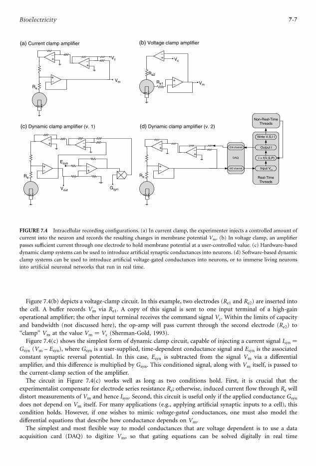
Figure 7.4(b) depicts a voltage-clamp circuit. In this example, two electrodes (Re1 and Re2) are inserted into
the cell. A buffer records Vm via Re1. A copy of this signal is sent to one input terminal of a high-gain
operational amplifier; the other input terminal receives the command signal Vc. Within the limits of capacity
and bandwidth (not discussed here), the op-amp will pass current through the second electrode (Re2) to
‘‘clamp’’ Vm at the value Vm ¼ Vc (Sherman-Gold, 1993).
Figure 7.4(c) shows the simplest form of dynamic clamp circuit, capable of injecting a current signal Isyn ¼Gsyn (Vm – Esyn), where Gsyn is a user-supplied, time-dependent conductance signal and Esyn is the associated
constant synaptic reversal potential. In this case, Esyn is subtracted from the signal Vm via a differential
amplifier, and this difference is multiplied by Gsyn. This conditioned signal, along with Vm itself, is passed to
the current-clamp section of the amplifier.
The circuit in Figure 7.4(c) works well as long as two conditions hold. First, it is crucial that the
experimentalist compensate for electrode series resistance Re; otherwise, induced current flow through Re will
distort measurements of Vm and hence Isyn. Second, this circuit is useful only if the applied conductance Gsyndoes not depend on Vm itself. For many applications (e.g., applying artificial synaptic inputs to a cell), this
condition holds. However, if one wishes to mimic voltage-gated conductances, one must also model the
differential equations that describe how conductance depends on Vm.
The simplest and most flexible way to model conductances that are voltage dependent is to use a data
acquisition card (DAQ) to digitize Vm, so that gating equations can be solved digitally in real time
(a) Current clamp amplifier (b) Voltage clamp amplifier
(c) Dynamic clamp amplifier (v. 1) (d) Dynamic clamp amplifier (v. 2)
Re
Re Re
Vout Gsyn
Esyn
Re2
Re1
Vc Vc
Vm Vm
+
+
−
−
+−
+−
+−
+−
+−+
−+−
+−
+−
+−
D/A channel
Non-Real-TimeThreads
Real-TimeThreads
Write V,S,I I
Output I
I = f(V,S,P)
Input VmA/D channel
DAQ
FIGURE 7.4 Intracellular recording configurations. (a) In current clamp, the experimenter injects a controlled amount of
current into the neuron and records the resulting changes in membrane potential Vm. (b) In voltage clamp, an amplifier
passes sufficient current through one electrode to hold membrane potential at a user-controlled value. (c) Hardware-based
dynamic clamp systems can be used to introduce artificial synaptic conductances into neurons. (d) Software-based dynamic
clamp systems can be used to introduce artificial voltage-gated conductances into neurons, or to immerse living neurons
into artificial neuronal networks that run in real time.
7-7Bioelectricity
(Figure 7.4(d)). The user interacts with the real-time thread via a GUI and other non-real-time threads
(Dorval et al., 2001). A number of systems of this type have been created and used to model even the fastest
conductance events in neurons (Prinz et al., 2004).
Models of Extracellular Stimulation
Thus far we have discussed intrinsic neuronal activation and the techniques used to examine naturally
occurring neuronal activity. We now turn our attention to external neuronal stimulation, a much older but
less thoroughly understood field. In 1791, Luigi Galvani publicized what he deemed ‘‘animal electricity,’’
supposedly generated by probing frog motor neurons with bimetallic rods. Two years later, Allessandro Volta
showed that Galvani’s animal electricity was actually a discharge of static electricity from the rod that activated
the nerve, and the field of extracellular stimulation was born. Little theoretical progress was made however,
until Hodgkin and Huxley elucidated the mechanisms of neuronal excitability in 1952. As stated previously,
the all-or-nothing action potential described by Hodgkin and Huxley initiates when the potential difference
across the membrane depolarizes to some threshold. This threshold-achieving depolarization is typically
generated via synaptic input coupling with membrane-intrinsic conductances, but can be achieved artificially
with a well-positioned electrode delivering an appropriate stimulus.
Consider membrane potential Vm as the difference between the intrinsic neuronal potential Vi and the
potential just external to the neuron Ve, both varying in time and space, defined with respect to the same
distant ground somewhere within the extracellular space: Vm(z,t) ¼ Vi(z,t) – Ve(z,t). Under physiological
conditions, the extracellular space is primarily isopotential but stimulation via a point electrode in an isotropic
extracellular space can shape Ve(z,t) according to:
Veðz; tÞ ¼ ½reIsðtÞ =½4px ð7:6Þ
where re is the resistivity of the extracellular space (typically ,300 O cm), x is the distance between the
electrode and the axon at location z, and Is(t) is the current applied through the electrode. From first
principles, Equation (7.6) can be extended to anisotropic, inhomogeneous media and more complex electrode
geometries.
To understand extracellular axonal stimulation, we revisit Equation (7.5) with the knowledge that the
axoplasm is isopotential except during action potentials or stimulation. Hence, under normal conditions, the
second spatial derivative of extracellular potential (along the length of the axon) drives axonal activation, and
is often referred to as the activating function, q2Ve=qz2:When the axon is at rest, qVm=qt must be positive for
the membrane to approach threshold. From Equation (7.5), we can deduce that positive deflections of the
activating function depolarize the membrane potential (Rattay, 1986). As an example, we consider a
stimulating electrode placed 1.0 mm from an infinitely long Hodgkin–Huxley axon. Figure 7.5(a) shows the
extracellular potential and activating function along an axon, in response to the minimum amplitude cathodic
and anodic stimuli capable of eliciting action potentials when applied for 0.1 msec. Action potential initiation
depends on the duration of the applied stimulus and the amplitude of the positive portion of the activating
function. Since cathodic stimulation yields a larger positive region of the activating function in response to a
smaller external field (and thus less applied current), cathodic stimulation initiates action potentials more
efficiently. Figure 7.5(b) depicts action potential propagation in the Hodgkin–Huxley model in response to
cathodic stimulus. Note that the action potential propagates in both directions from the site of origin.
Not all stimuli are strong enough to elicit an action potential. Figure 7.6(a) shows membrane potential vs.
time for a patch of axonal membrane at z ¼ 0, in response to four different cathodic stimuli. Electrode and
model configuration are the same as in the previous figure. In general, the smaller the stimulus amplitude, the
longer it must be applied for an axon to reach threshold. Some stimuli are so small, however, that even if they
were applied forever they would not elicit an action potential. The smallest amplitude stimulus capable of
generating a response is known as the rheobase. The chronaxie is the required duration to generate an action
potential using a stimulus whose amplitude is twice the rheobase. Rheobase and chronaxie vary greatly across
experimental conditions: electrode size and position, axon radius, conductance distributions, and the presence
7-8 Sensors, Nanoscience, Biomedical Engineering, and Instruments
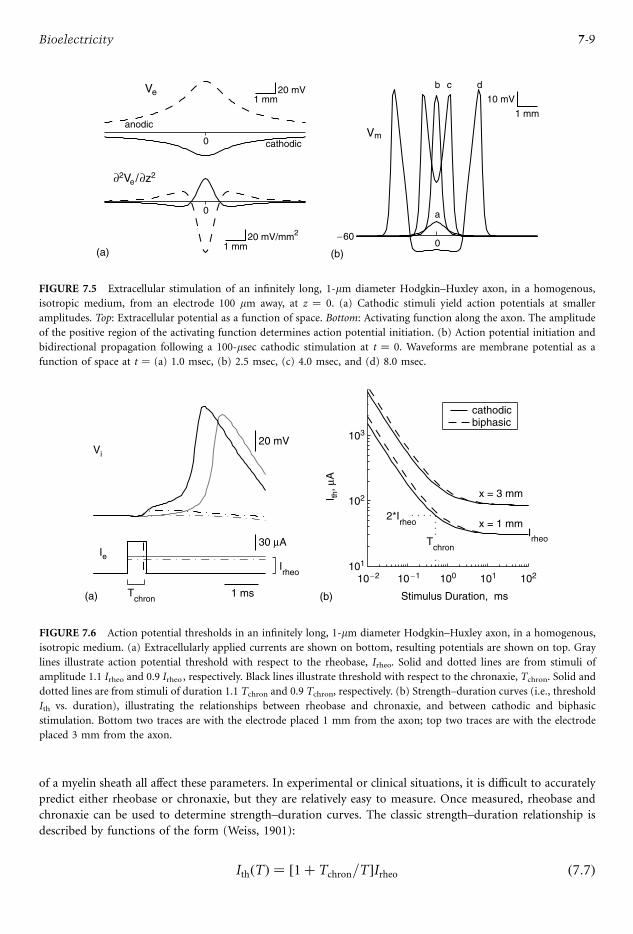
of a myelin sheath all affect these parameters. In experimental or clinical situations, it is difficult to accurately
predict either rheobase or chronaxie, but they are relatively easy to measure. Once measured, rheobase and
chronaxie can be used to determine strength–duration curves. The classic strength–duration relationship is
described by functions of the form (Weiss, 1901):
IthðTÞ ¼ ½1þ Tchron=T Irheo ð7:7Þ
Vi
Ie
20 mV
30 μA
1 ms
Irheo
Tchron
10−2 10 −1 100 101 102101
102
103
I th,μ
A
Stimulus Duration, ms
Irheo
2*Irheo
Tchron
x = 3 mm
x = 1 mm
cathodicbiphasic
(a) (b)
FIGURE 7.6 Action potential thresholds in an infinitely long, 1-mm diameter Hodgkin–Huxley axon, in a homogenous,
isotropic medium. (a) Extracellularly applied currents are shown on bottom, resulting potentials are shown on top. Gray
lines illustrate action potential threshold with respect to the rheobase, Irheo. Solid and dotted lines are from stimuli of
amplitude 1.1 Irheo and 0.9 Irheo , respectively. Black lines illustrate threshold with respect to the chronaxie, Tchron. Solid and
dotted lines are from stimuli of duration 1.1 Tchron and 0.9 Tchron, respectively. (b) Strength–duration curves (i.e., threshold
Ith vs. duration), illustrating the relationships between rheobase and chronaxie, and between cathodic and biphasic
stimulation. Bottom two traces are with the electrode placed 1 mm from the axon; top two traces are with the electrode
placed 3 mm from the axon.
∂2Ve/∂z2
0
1 mm20 mV/mm2
(a) (b)
Ve
0
1 mm20 mV
anodic
cathodicVm
0−60
10 mV
1 mm
a
b c d
FIGURE 7.5 Extracellular stimulation of an infinitely long, 1-mm diameter Hodgkin–Huxley axon, in a homogenous,
isotropic medium, from an electrode 100 mm away, at z ¼ 0. (a) Cathodic stimuli yield action potentials at smaller
amplitudes. Top: Extracellular potential as a function of space. Bottom: Activating function along the axon. The amplitude
of the positive region of the activating function determines action potential initiation. (b) Action potential initiation and
bidirectional propagation following a 100-msec cathodic stimulation at t ¼ 0. Waveforms are membrane potential as a
function of space at t ¼ (a) 1.0 msec, (b) 2.5 msec, (c) 4.0 msec, and (d) 8.0 msec.
7-9Bioelectricity

where T is the stimulus duration, Ith is the minimum applied current required to induce an action potential,
Tchron is the chronaxie, and Irheo is the rheobase. The solid lines of Figure 7.6b display strength–duration
curves for a Hodgkin–Huxley axon stimulated by electrodes at two distances from the axon.
The monophasic stimulation discussed so far is often unsuitable for clinical use because it encourages
charge buildup on the electrode upon repeated bouts of stimulation. To reduce charge buildup, cathodic
pulses are often followed by equal-amplitude–anodic pulses to create biphasic stimulation that delivers no net
charge through the electrode. The rheobase for biphasic stimuli is the same as for monophasic cathodic
because the action potential occurs during the cathodic stimulation in either case. For stronger but shorter
applied currents (e.g., at the chronaxie) action potentials actually occur after the cathodic stimulus has ended.
In the biphasic stimulus case, the anodic phase interacts with membrane potential before action potential
generation. Hence, for short-duration stimuli, biphasic currents require slightly larger amplitudes than
monophasic currents (compare dashed and solid lines in Figure 7.6(b)).
In living organisms, axons rarely exist in isolation. Axons of various sizes are typically bound together in a
nerve bundle that travels between brain regions or from the brain to elsewhere in the body. Hence, in vivo
considerations of extracellular stimulation focus on the recruitment of multiple axons within a nerve. That is,
for a given amplitude stimulus, a certain number of axons within a nerve will be recruited, or fire action
potentials. For a larger amplitude stimulus, a larger number of axons will be recruited. Axonal diameter and
distance from the electrode will determine which axons are recruited and in what order. As demonstrated by
Figure 7.6(b), a couple of millimeters can make a large difference in axonal excitability.
Unlike the neurons thus far examined, living axons are not perfect cylinders residing in homogenous,
isotropic media. Thus, any consideration of in vivo extracellular stimulation must include details about the
organism that we have heretofore overlooked. For real systems, extracellular resistivity re varies as a functionof space. For example, the extracellular medium is likely to be more conductive in the direction of a bundle of
nerves, and more resistive perpendicular to the bundle. Anisotropies of this type change the extracellular
potential experienced by any local axon, and thus modify the susceptibility to electrical stimulation. In
many cases these differences alter the qualitative behavior of the system (e.g., the order in which axons in a
nerve are recruited depends on subtle differences in the extracellular resistivity anisotropy). These
modifications can be worked out analytically for some configurations, but are beyond the scope of this
chapter (see Grill, 1999).
Application: Deep Brain Stimulation
While the details of neural activation via extracellular stimulation continue to be elucidated, the underlying
principles described in the previous section have been understood for decades. With this knowledge,
researchers and physicians have devised a number of ways that extracellular stimulation can be used to treat
medical conditions. Some of these techniques have been used clinically since the 1970s, others are relatively
new, and many more are still being developed. Like many medical technologies, extracellular stimulation has
practical complications unrelated to a scientific understanding of the problem, which pose obstacles for
clinical implementation (Davis, 2002).
Clinical applications of electrical stimulation can be divided into three categories:
1. Neural output activation involves electrical stimulation of nerves that control some output function of
the nervous system. For example, stimulation of peripheral nerves is used to provide some skeletal muscle
control to quadriplegics and other individuals afflicted with motor deficits (Sinkjaer et al., 2003). Direct
stimulation of the spinal cord is now being used to return bladder and sphincter control to paraplegics
and patients suffering from incontinence (Jezernik et al., 2002).
2. Neural input activation is used to bypass defective sense organs. By electrically stimulating the auditory
nerve, cochlear implants provide a sense of hearing sufficient for previously deaf individuals to
understand speech (Skinner, 2003). On a more experimental frontier, retinal implants have had some
success restoring sight to the visually impaired by electrically stimulating retinal neurons at the back of
the eye (Hetling and Baig-Silva, 2004).
7-10 Sensors, Nanoscience, Biomedical Engineering, and Instruments
3. Central nervous system processing activation treats diseases located more centrally within the nervous
system than the previous two classes. Electroconvulsive therapy, in its current form, is often an effective
treatment for individuals suffering from severe depression (Reisner, 2003). Deep brain stimulation (DBS),
a more recent and less controversial form of brain stimulation, lessens the debilitating effects of
Parkinson’s disease, and shows promise as a treatment for a number of other diseases of the central
nervous system.
As an example of extracellular stimulation in use clinically, we briefly explore DBS. This clinically effective
treatment reduces the symptoms of many motor disorders, including Parkinson’s disease, essential tremor, and
multiple sclerosis. For DBS, a chronic electrode is placed in some brain region — typically the thalamus or
basal ganglia for treatment of motor disorders. High-frequency (100 to 250 Hz) current is passed through the
electrode to the surrounding neural tissue. Amazingly, signs of malfunction such as rigidity or tremor are
reduced. Exactly how stimulation of certain regions reduces these symptoms is poorly understood. In fact,
exactly what populations of neurons are excited by electrical stimulation is still largely unknown.
The stimulating electrode is placed in a heterogeneous region of the brain that consists of neuronal cell
bodies and axons of passage (axons just passing through the region). Since local cells and axons of passage can
project to widely different brain regions, it is of utmost importance to know which group is stimulated. As we
know from the previous section, electrical stimulation excites infinitely long, cylindrical axons at the positive
peak of the relatively simple activating function (Figure 7.5). Not surprisingly, the effects of stimulation are
more complicated for finite, noncylindrical membranes. Geometric differences between cell bodies and axons
lead to widely varying stimulus–duration curves. In some cases, simple knowledge of the rheobases and
chronaxies may allow for the differential excitation of either axons or cell bodies simply by delivering modified
stimulus waveforms (Grill and McIntyre, 2001).
From models and experiments we know that DBS inhibits cell bodies near the electrode but excites the
output axons of those cells. How this complex activity translates to improved motor function is still largely
unknown. One model of DBS suggests that stimulation causes an over-excitation of axons leaving the region.
This over-excitation actually leads to decreased action potential generation via a mechanism known as
depolarization blockade. Another model suggests that DBS works primarily by exciting inhibitory neurons
which then suppress the cells to which they project. In contrast to these excitation-vs.-inhibition approaches,
newer models incorporate action potential firing times into a theory of DBS function (Grill et al., 2004).
Clinical data and continued modeling will soon determine which of these approaches accurately models the
mechanisms of DBS. For more details on recent developments in deep brain stimulation, see McIntyre (2004).
The mechanisms by which DBS (and other stimulation techniques) benefits patients are slowly being
elucidated. Theoretical results from the basic understandings laid out in this section are likely to be
incorporated into experimental and clinical work. As understanding of electrical stimulation grows, so does
ubiquity of use and the number of conceivable clinical applications.
Glossary of Terms
Action potential: The all-or-nothing electrical impulse used to communicate information between
neurons and from neurons to muscle fibers.
Activating function: The second spatial derivative of extracellular potential determines where a neuron
will be excited to produce an action potential.
Activation: A term referring to the time- and voltage-dependent growth of a membrane’s conductance
after membrane depolarization.
Chronaxie: The minimum duration of time required for a stimulus twice the amplitude of the rheobase to
induce an action potential.
Current clamp: An experimental protocol in which transmembrane current is controlled, usually at a
series of constant values, and resulting transmembrane potentials are measured.
Dynamic clamp: An experimental protocol in which circuitry, often along with a real-time computer
program, is used to mimic membrane conductances.
7-11Bioelectricity

Inactivation: The time- and voltage-dependent decline of the Naþ conductance, which follows shortly
after its activation.
Ligand-gated ion channels: Transmembrane proteins that open in response to changes in the
extracellular concentration of a particular neurotransmitter (ligand).
Membrane potential: The voltage difference across the neural membrane.
Refractory period: The period immediately after an action potential, in which it is difficult or impossible
to induce a second action potential.
Rheobase: The minimum current, when provided for an infinite duration, capable of inducing a neuron to
fire an action potential.
Space clamp: The condition inwhichmembrane potential is the same throughout the spatial extent of the cell.
Voltage clamp: An experimental protocol in which membrane potential is controlled, usually in a stepwise
fashion, and resulting transmembrane currents are measured.
Voltage-gated ion channels: Transmembrane proteins that open in response to changes in membrane
potential, allowing a particular ionic species to cross the membrane.
References
R. Davis, ‘‘Twenty-eight years of clinical experience with implantable neuroprostheses for various
applications,’’ Artif. Organs, 26, 280–283, 2002.
A.D. Dorval, D.J. Christini, and J.A. White, ‘‘Real-time linux dynamic clamp: a fast and flexible way to
construct virtual ion channels in living cells,’’ Ann. Biomed. Eng., 29, 897–907, 2001.
D.A. Doyle Morais, J. Cabral, R.A. Pfuetzner, A. Kuo, J.M. Gulbis, S.L. Cohen, B.T. Chait, and R. MacKinnon,
‘‘The structure of the potassium channel: molecular basis of Kþ conduction and selectivity,’’ Science,
280, 69–77, 1998.
W.M. Grill Jr., ‘‘Modeling the effects of electric fields on nerve fibers: influence of tissue electrical properties,’’
IEEE Trans. Biomed. Eng., 46, 918–928, 1999.
W.M. Grill, Jr. and C.C. McIntyre, ‘‘Extracellular excitation of central neurons: implications for the
mechanisms of deep brain stimulation,’’ Thalamus Relat. Sys., 1, 269–277, 2001.
J.R. Hetling and M.S. Baig-Silva, ‘‘Neural prostheses for vision: designing a functional interface with retinal
neurons,’’ Neurol. Res., 26, 21–34, 2004.
A.L. Hodgkin and A.F. Huxley, ‘‘A quantitative description of membrane current and its application to
conduction and excitation in nerve,’’ J. Physiol., 117, 500–544, 1952.
S. Jezernik, M. Craggs, W.M. Grill, G. Creasey, and N.J. Rijkhoff, ‘‘Electrical stimulation for the treatment of
bladder dysfunction: current status and future possibilities,’’ Neurol. Res., 24, 413–430, 2002.
C.C. McIntyre, M. Savasta, B.L. Walter, and J.L. Vitek, ‘‘How does deep brain stimulation work? Present
understanding and future questions,’’ J. Clin. Neurophysiol., 21, 40–50, 2004.
A.A. Prinz, L.F. Abbott, and E.Marder, ‘‘The dynamic clamp comes of age,’’ Trends. Neurosci., 27, 218–224, 2004.
F. Rattay, ‘‘Analysis of models for external stimulation of axons,’’ IEEE Trans. Biomed. Eng., 33, 974–977, 1986.
A.D. Reisner, ‘‘The electroconvulsive therapy controversy: evidence and ethics,’’ Neuropsychol. Rev., 13,
199–219, 2003.
B. Sakmann and E. Neher, Single-Channel Recording, 2nd ed., New York: Plenum Press, 1995.
R. Sherman-Gold, Ed., The Axon Guide, Foster City, CA: Axon Instruments, Inc., 1993.
T. Sinkjaer, M. Haugland, A. Inmann, M. Hansen, and K.D. Nielsen, ‘‘Biopotentials as command and feedback
signals in functional electrical stimulation systems,’’ Med. Eng. Phys., 25, 29–40, 2003.
M.W. Skinner, ‘‘Optimizing cochlear implant speech performance,’’ Ann. Otol. Rhinol. Laryngol. Suppl., 191,
4–13, 2003.
G.G. Weiss, ‘‘Sur la possibilite de rendre comparables entre eux les appareils: a l’excitation,’’ Arch. Ital. Biol., 35,
413–445, 1901.
T. Weiss, Cellular Biophysics, Cambridge, MA: MIT Press, 1996.
J.A. White, ‘‘Action potential,’’ in Encyclopedia of the Human Brain, V.S. Ramachandran, Ed., San Diego,
CA: Academic Press, 2002, pp. 1–12.
7-12 Sensors, Nanoscience, Biomedical Engineering, and Instruments
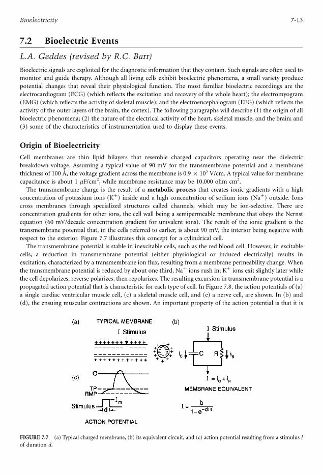
7.2 Bioelectric Events
L.A. Geddes (revised by R.C. Barr)
Bioelectric signals are exploited for the diagnostic information that they contain. Such signals are often used to
monitor and guide therapy. Although all living cells exhibit bioelectric phenomena, a small variety produce
potential changes that reveal their physiological function. The most familiar bioelectric recordings are the
electrocardiogram (ECG) (which reflects the excitation and recovery of the whole heart); the electromyogram
(EMG) (which reflects the activity of skeletal muscle); and the electroencephalogram (EEG) (which reflects the
activity of the outer layers of the brain, the cortex). The following paragraphs will describe (1) the origin of all
bioelectric phenomena; (2) the nature of the electrical activity of the heart, skeletal muscle, and the brain; and
(3) some of the characteristics of instrumentation used to display these events.
Origin of Bioelectricity
Cell membranes are thin lipid bilayers that resemble charged capacitors operating near the dielectric
breakdown voltage. Assuming a typical value of 90 mV for the transmembrane potential and a membrane
thickness of 100 A, the voltage gradient across the membrane is 0.9 · 105 V/cm. A typical value for membrane
capacitance is about 1 mF/cm2, while membrane resistance may be 10,000 ohm cm2.
The transmembrane charge is the result of a metabolic process that creates ionic gradients with a high
concentration of potassium ions (Kþ) inside and a high concentration of sodium ions (Naþ) outside. Ionscross membranes through specialized structures called channels, which may be ion-selective. There are
concentration gradients for other ions, the cell wall being a semipermeable membrane that obeys the Nernst
equation (60 mV/decade concentration gradient for univalent ions). The result of the ionic gradient is the
transmembrane potential that, in the cells referred to earlier, is about 90 mV, the interior being negative with
respect to the exterior. Figure 7.7 illustrates this concept for a cylindrical cell.
The transmembrane potential is stable in inexcitable cells, such as the red blood cell. However, in excitable
cells, a reduction in transmembrane potential (either physiological or induced electrically) results in
excitation, characterized by a transmembrane ion flux, resulting from a membrane permeability change. When
the transmembrane potential is reduced by about one third, Naþ ions rush in; Kþ ions exit slightly later whilethe cell depolarizes, reverse polarizes, then repolarizes. The resulting excursion in transmembrane potential is a
propagated action potential that is characteristic for each type of cell. In Figure 7.8, the action potentials of (a)
a single cardiac ventricular muscle cell, (c) a skeletal muscle cell, and (e) a nerve cell, are shown. In (b) and
(d), the ensuing muscular contractions are shown. An important property of the action potential is that it is
FIGURE 7.7 (a) Typical charged membrane, (b) its equivalent circuit, and (c) action potential resulting from a stimulus I
of duration d.
7-13Bioelectricity
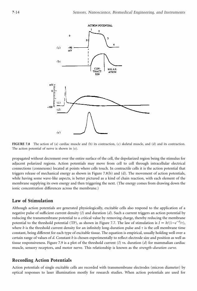
propagated without decrement over the entire surface of the cell, the depolarized region being the stimulus for
adjacent polarized regions. Action potentials may move from cell to cell through intracellular electrical
connections (connexons) located at points where cells touch. In contractile cells it is the action potential that
triggers release of mechanical energy as shown in Figure 7.8(b) and (d). The movement of action potentials,
while having some wave-like aspects, is better pictured as a kind of chain reaction, with each element of the
membrane supplying its own energy and then triggering the next. (The energy comes from drawing down the
ionic concentration differences across the membrane.)
Law of Stimulation
Although action potentials are generated physiologically, excitable cells also respond to the application of a
negative pulse of sufficient current density (I) and duration (d). Such a current triggers an action potential by
reducing the transmembrane potential to a critical value by removing charge, thereby reducing the membrane
potential to the threshold potential (TP), as shown in Figure 7.7. The law of stimulation is I ¼ b/(1 e d/t),where b is the threshold current density for an infinitely long-duration pulse and t is the cell membrane timeconstant, being different for each type of excitable tissue. The equation is empirical, usually holding well over a
certain range of values of d. Constant b is chosen experimentally to reflect electrode size and position as well as
tissue responsiveness. Figure 7.9 is a plot of the threshold current (I) vs. duration (d) for mammalian cardiac
muscle, sensory receptors, and motor nerve. This relationship is known as the strength–duration curve.
Recording Action Potentials
Action potentials of single excitable cells are recorded with transmembrane electrodes (micron diameter) by
optical responses to laser illumination mostly for research studies. When action potentials are used for
FIGURE 7.8 The action of (a) cardiac muscle and (b) its contraction, (c) skeletal muscle, and (d) and its contraction.
The action potential of nerve is shown in (e).
7-14 Sensors, Nanoscience, Biomedical Engineering, and Instruments
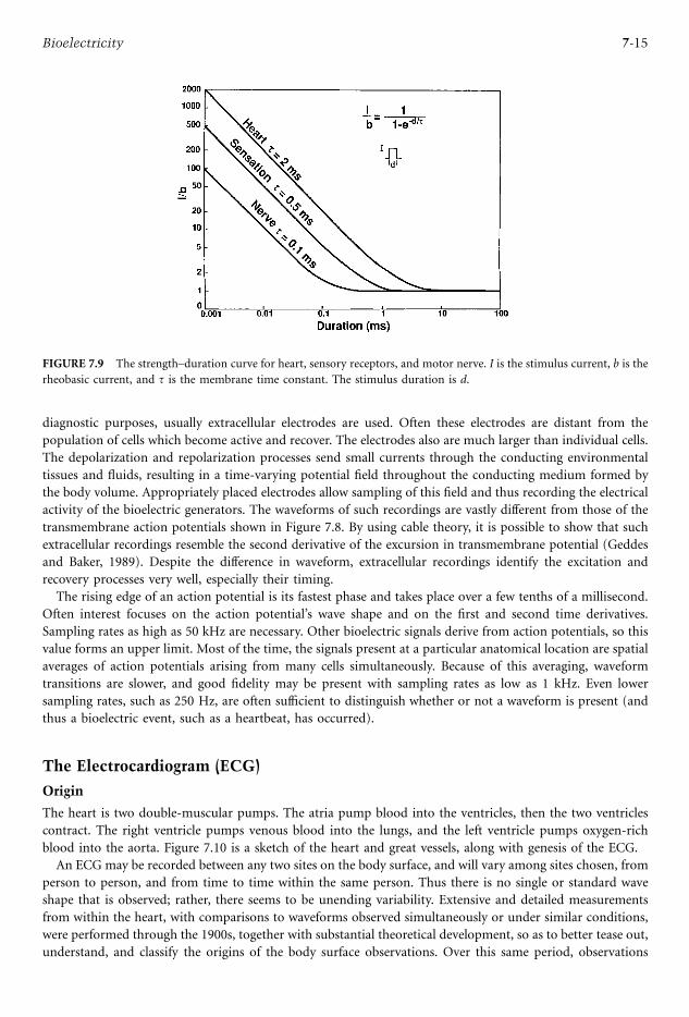
diagnostic purposes, usually extracellular electrodes are used. Often these electrodes are distant from the
population of cells which become active and recover. The electrodes also are much larger than individual cells.
The depolarization and repolarization processes send small currents through the conducting environmental
tissues and fluids, resulting in a time-varying potential field throughout the conducting medium formed by
the body volume. Appropriately placed electrodes allow sampling of this field and thus recording the electrical
activity of the bioelectric generators. The waveforms of such recordings are vastly different from those of the
transmembrane action potentials shown in Figure 7.8. By using cable theory, it is possible to show that such
extracellular recordings resemble the second derivative of the excursion in transmembrane potential (Geddes
and Baker, 1989). Despite the difference in waveform, extracellular recordings identify the excitation and
recovery processes very well, especially their timing.
The rising edge of an action potential is its fastest phase and takes place over a few tenths of a millisecond.
Often interest focuses on the action potential’s wave shape and on the first and second time derivatives.
Sampling rates as high as 50 kHz are necessary. Other bioelectric signals derive from action potentials, so this
value forms an upper limit. Most of the time, the signals present at a particular anatomical location are spatial
averages of action potentials arising from many cells simultaneously. Because of this averaging, waveform
transitions are slower, and good fidelity may be present with sampling rates as low as 1 kHz. Even lower
sampling rates, such as 250 Hz, are often sufficient to distinguish whether or not a waveform is present (and
thus a bioelectric event, such as a heartbeat, has occurred).
The Electrocardiogram (ECG)
Origin
The heart is two double-muscular pumps. The atria pump blood into the ventricles, then the two ventricles
contract. The right ventricle pumps venous blood into the lungs, and the left ventricle pumps oxygen-rich
blood into the aorta. Figure 7.10 is a sketch of the heart and great vessels, along with genesis of the ECG.
An ECG may be recorded between any two sites on the body surface, and will vary among sites chosen, from
person to person, and from time to time within the same person. Thus there is no single or standard wave
shape that is observed; rather, there seems to be unending variability. Extensive and detailed measurements
from within the heart, with comparisons to waveforms observed simultaneously or under similar conditions,
were performed through the 1900s, together with substantial theoretical development, so as to better tease out,
understand, and classify the origins of the body surface observations. Over this same period, observations
FIGURE 7.9 The strength–duration curve for heart, sensory receptors, and motor nerve. I is the stimulus current, b is the
rheobasic current, and t is the membrane time constant. The stimulus duration is d.
7-15Bioelectricity
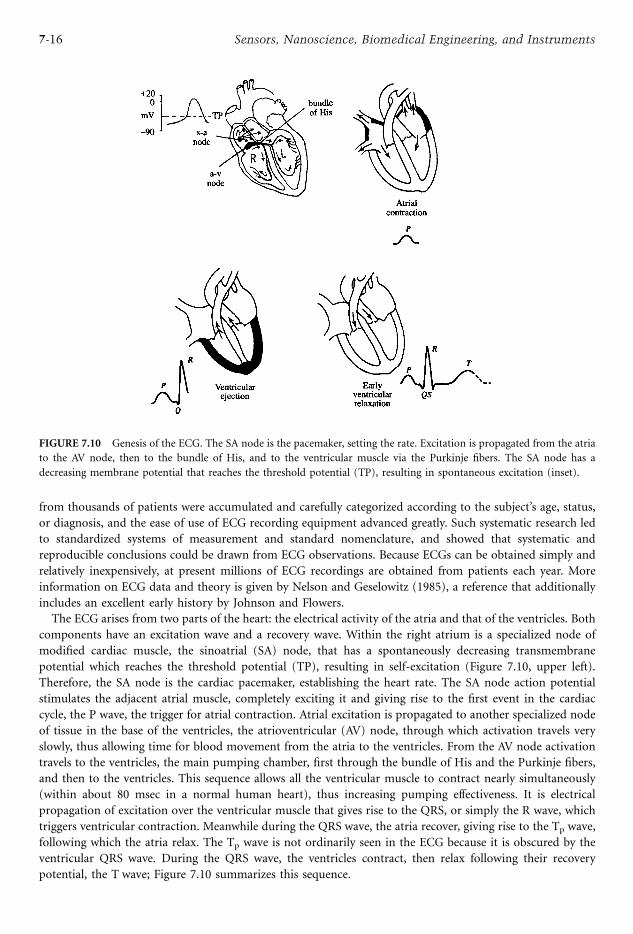
from thousands of patients were accumulated and carefully categorized according to the subject’s age, status,
or diagnosis, and the ease of use of ECG recording equipment advanced greatly. Such systematic research led
to standardized systems of measurement and standard nomenclature, and showed that systematic and
reproducible conclusions could be drawn from ECG observations. Because ECGs can be obtained simply and
relatively inexpensively, at present millions of ECG recordings are obtained from patients each year. More
information on ECG data and theory is given by Nelson and Geselowitz (1985), a reference that additionally
includes an excellent early history by Johnson and Flowers.
The ECG arises from two parts of the heart: the electrical activity of the atria and that of the ventricles. Both
components have an excitation wave and a recovery wave. Within the right atrium is a specialized node of
modified cardiac muscle, the sinoatrial (SA) node, that has a spontaneously decreasing transmembrane
potential which reaches the threshold potential (TP), resulting in self-excitation (Figure 7.10, upper left).
Therefore, the SA node is the cardiac pacemaker, establishing the heart rate. The SA node action potential
stimulates the adjacent atrial muscle, completely exciting it and giving rise to the first event in the cardiac
cycle, the P wave, the trigger for atrial contraction. Atrial excitation is propagated to another specialized node
of tissue in the base of the ventricles, the atrioventricular (AV) node, through which activation travels very
slowly, thus allowing time for blood movement from the atria to the ventricles. From the AV node activation
travels to the ventricles, the main pumping chamber, first through the bundle of His and the Purkinje fibers,
and then to the ventricles. This sequence allows all the ventricular muscle to contract nearly simultaneously
(within about 80 msec in a normal human heart), thus increasing pumping effectiveness. It is electrical
propagation of excitation over the ventricular muscle that gives rise to the QRS, or simply the R wave, which
triggers ventricular contraction. Meanwhile during the QRS wave, the atria recover, giving rise to the Tp wave,
following which the atria relax. The Tp wave is not ordinarily seen in the ECG because it is obscured by the
ventricular QRS wave. During the QRS wave, the ventricles contract, then relax following their recovery
potential, the T wave; Figure 7.10 summarizes this sequence.
FIGURE 7.10 Genesis of the ECG. The SA node is the pacemaker, setting the rate. Excitation is propagated from the atria
to the AV node, then to the bundle of His, and to the ventricular muscle via the Purkinje fibers. The SA node has a
decreasing membrane potential that reaches the threshold potential (TP), resulting in spontaneous excitation (inset).
7-16 Sensors, Nanoscience, Biomedical Engineering, and Instruments

Ordinarily, the Tp wave is not visible. However, if the propagation of excitation from the atria to the
ventricles is blocked, the Tp wave can be seen. Figure 7.11 is a record of the ECG from a limb lead and a
recording from a lead within the right atrium in a subject with transient AV block. Note that the sharp P wave
in the atrial lead coincides with the P wave in the limb recording and that the atrial lead shows both P and Tpwaves, easily identified during AV block.
Clinical Significance
From the foregoing it can be seen that the ECG is effective as a timing signal. There may also be dynamic
information in its amplitude or wave shape, with the latter normally determined by historical comparison to
previous groups of subjects or patients. By observing the orderly P–QRS–T sequence both as to timing and
wave form it is possible to determine if the excitatory and recovery processes in the heart are functioning
normally.
Disturbances in the orderly timing of the cardiac cycle are elegantly displayed by the ECG. For example,
each atrial excitation may not be delivered to the AV node. AV block exists when there is less than a 1/1
correspondence between the P and QRS complexes (Figure 7.11).
Figure 7.12(1) shows a normal ECG and Figure 7.12(2) illustrates a 2/1 AV block with two P waves for each
QRS–T complex. Complete AV block exists when none of the atrial excitations reach the AV node, as shown in
Figure 7.12(3). In this case the ventricles developed their own rhythm, which was slow; cardiac output is low,
and in such a situation an artificial pacemaker must be implanted.
For many reasons, the atria develop a rapid rate called atrial tachycardia or supraventricular tachycardia.
A very rapid atrial rate is designated atrial flutter (Figure 7.12(4)). With both atrial tachycardia and flutter, the
atrial contractions are coordinated, although the ventricular pumping capability is reduced owing to
inadequate filling time. The ventricles are driven at a rapid rate, and cardiac output is low.
Atrial fibrillation is an electrical dysrhythmia in which all the atrial muscle fibers are contracting and
relaxing asynchronously and there is no atrial pumping. This dysrhythmia (Figure 7.12(5)) causes the
ventricles to be excited at a very rapid and irregular rate. Cardiac output is reduced, and the pulse is rapid and
irregular in force and rate.
If the propagation of excitation in the ventricles is impaired by damage to the bundle of His, the
coordination of excitation and contraction is impaired and reveals itself by a widening of the QRS wave, and
often a notch is present; Figure 7.12(6) illustrates right (RBBB) and left (LBBB) bundle-branch block. These
waveforms are best identified in the chest (V) leads.
All parts of the heart are capable of exhibiting rhythmic activity, there being a rhythmicity hierarchy from
the SA node to the ventricular muscle. In abnormal circumstances, the atria and ventricles generate
spontaneous beats. Such ectopic excitations do not propagate through the structures of the heart in the same
sequence, so the ECG waveforms are different. Figure 7.12(7) illustrates ventricular ectopic beats in which the
FIGURE 7.11 Lead 2 ECG and an atrial lead. In the center of the record AV block was produced, showing the P waves in
lead 2 and the P and Tp waves in the atrial lead.
7-17Bioelectricity
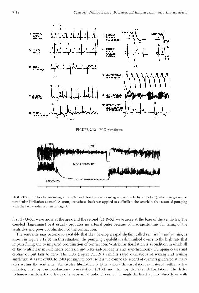
first (l) Q–S,T wave arose at the apex and the second (2) R–S,T wave arose at the base of the ventricles. The
coupled (bigeminus) beat usually produces no arterial pulse because of inadequate time for filling of the
ventricles and poor coordination of the contraction.
The ventricles may become so excitable that they develop a rapid rhythm called ventricular tachycardia, as
shown in Figure 7.12(8). In this situation, the pumping capability is diminished owing to the high rate that
impairs filling and to impaired coordination of contraction. Ventricular fibrillation is a condition in which all
of the ventricular muscle fibers contract and relax independently and asynchronously. Pumping ceases and
cardiac output falls to zero. The ECG (Figure 7.12(9)) exhibits rapid oscillations of waxing and waning
amplitude at a rate of 800 to 1500 per minute because it is the composite record of currents generated at many
sites within the ventricles. Ventricular fibrillation is lethal unless the circulation is restored within a few
minutes, first by cardiopulmonary resuscitation (CPR) and then by electrical defibrillation. The latter
technique employs the delivery of a substantial pulse of current through the heart applied directly or with
FIGURE 7.12 ECG waveforms.
FIGURE 7.13 The electrocardiogram (ECG) and blood pressure during ventricular tachycardia (left), which progressed to
ventricular fibrillation (center). A strong transchest shock was applied to defibrillate the ventricles that resumed pumping
with the tachycardia returning (right).
7-18 Sensors, Nanoscience, Biomedical Engineering, and Instruments
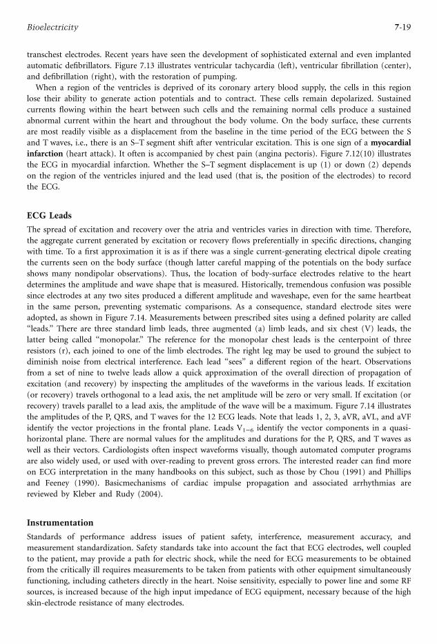
transchest electrodes. Recent years have seen the development of sophisticated external and even implanted
automatic defibrillators. Figure 7.13 illustrates ventricular tachycardia (left), ventricular fibrillation (center),
and defibrillation (right), with the restoration of pumping.
When a region of the ventricles is deprived of its coronary artery blood supply, the cells in this region
lose their ability to generate action potentials and to contract. These cells remain depolarized. Sustained
currents flowing within the heart between such cells and the remaining normal cells produce a sustained
abnormal current within the heart and throughout the body volume. On the body surface, these currents
are most readily visible as a displacement from the baseline in the time period of the ECG between the S
and T waves, i.e., there is an S–T segment shift after ventricular excitation. This is one sign of a myocardial
infarction (heart attack). It often is accompanied by chest pain (angina pectoris). Figure 7.12(10) illustrates
the ECG in myocardial infarction. Whether the S–T segment displacement is up (1) or down (2) depends
on the region of the ventricles injured and the lead used (that is, the position of the electrodes) to record
the ECG.
ECG Leads
The spread of excitation and recovery over the atria and ventricles varies in direction with time. Therefore,
the aggregate current generated by excitation or recovery flows preferentially in specific directions, changing
with time. To a first approximation it is as if there was a single current-generating electrical dipole creating
the currents seen on the body surface (though latter careful mapping of the potentials on the body surface
shows many nondipolar observations). Thus, the location of body-surface electrodes relative to the heart
determines the amplitude and wave shape that is measured. Historically, tremendous confusion was possible
since electrodes at any two sites produced a different amplitude and waveshape, even for the same heartbeat
in the same person, preventing systematic comparisons. As a consequence, standard electrode sites were
adopted, as shown in Figure 7.14. Measurements between prescribed sites using a defined polarity are called
‘‘leads.’’ There are three standard limb leads, three augmented (a) limb leads, and six chest (V) leads, the
latter being called ‘‘monopolar.’’ The reference for the monopolar chest leads is the centerpoint of three
resistors (r), each joined to one of the limb electrodes. The right leg may be used to ground the subject to
diminish noise from electrical interference. Each lead ‘‘sees’’ a different region of the heart. Observations
from a set of nine to twelve leads allow a quick approximation of the overall direction of propagation of
excitation (and recovery) by inspecting the amplitudes of the waveforms in the various leads. If excitation
(or recovery) travels orthogonal to a lead axis, the net amplitude will be zero or very small. If excitation (or
recovery) travels parallel to a lead axis, the amplitude of the wave will be a maximum. Figure 7.14 illustrates
the amplitudes of the P, QRS, and T waves for the 12 ECG leads. Note that leads 1, 2, 3, aVR, aVL, and aVF
identify the vector projections in the frontal plane. Leads V1 6 identify the vector components in a quasi-
horizontal plane. There are normal values for the amplitudes and durations for the P, QRS, and T waves as
well as their vectors. Cardiologists often inspect waveforms visually, though automated computer programs
are also widely used, or used with over-reading to prevent gross errors. The interested reader can find more
on ECG interpretation in the many handbooks on this subject, such as those by Chou (1991) and Phillips
and Feeney (1990). Basicmechanisms of cardiac impulse propagation and associated arrhythmias are
reviewed by Kleber and Rudy (2004).
Instrumentation
Standards of performance address issues of patient safety, interference, measurement accuracy, and
measurement standardization. Safety standards take into account the fact that ECG electrodes, well coupled
to the patient, may provide a path for electric shock, while the need for ECG measurements to be obtained
from the critically ill requires measurements to be taken from patients with other equipment simultaneously
functioning, including catheters directly in the heart. Noise sensitivity, especially to power line and some RF
sources, is increased because of the high input impedance of ECG equipment, necessary because of the high
skin-electrode resistance of many electrodes.
7-19Bioelectricity
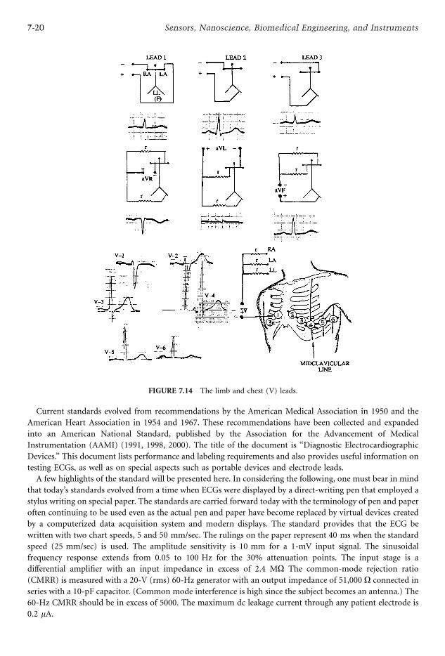
Current standards evolved from recommendations by the American Medical Association in 1950 and the
American Heart Association in 1954 and 1967. These recommendations have been collected and expanded
into an American National Standard, published by the Association for the Advancement of Medical
Instrumentation (AAMI) (1991, 1998, 2000). The title of the document is ‘‘Diagnostic Electrocardiographic
Devices.’’ This document lists performance and labeling requirements and also provides useful information on
testing ECGs, as well as on special aspects such as portable devices and electrode leads.
A few highlights of the standard will be presented here. In considering the following, one must bear in mind
that today’s standards evolved from a time when ECGs were displayed by a direct-writing pen that employed a
stylus writing on special paper. The standards are carried forward today with the terminology of pen and paper
often continuing to be used even as the actual pen and paper have become replaced by virtual devices created
by a computerized data acquisition system and modern displays. The standard provides that the ECG be
written with two chart speeds, 5 and 50 mm/sec. The rulings on the paper represent 40 ms when the standard
speed (25 mm/sec) is used. The amplitude sensitivity is 10 mm for a 1-mV input signal. The sinusoidal
frequency response extends from 0.05 to 100 Hz for the 30% attenuation points. The input stage is a
differential amplifier with an input impedance in excess of 2.4 MO The common-mode rejection ratio
(CMRR) is measured with a 20-V (rms) 60-Hz generator with an output impedance of 51,000 O connected in
series with a 10-pF capacitor. (Common mode interference is high since the subject becomes an antenna.) The
60-Hz CMRR should be in excess of 5000. The maximum dc leakage current through any patient electrode is
0.2 mA.
FIGURE 7.14 The limb and chest (V) leads.
7-20 Sensors, Nanoscience, Biomedical Engineering, and Instruments
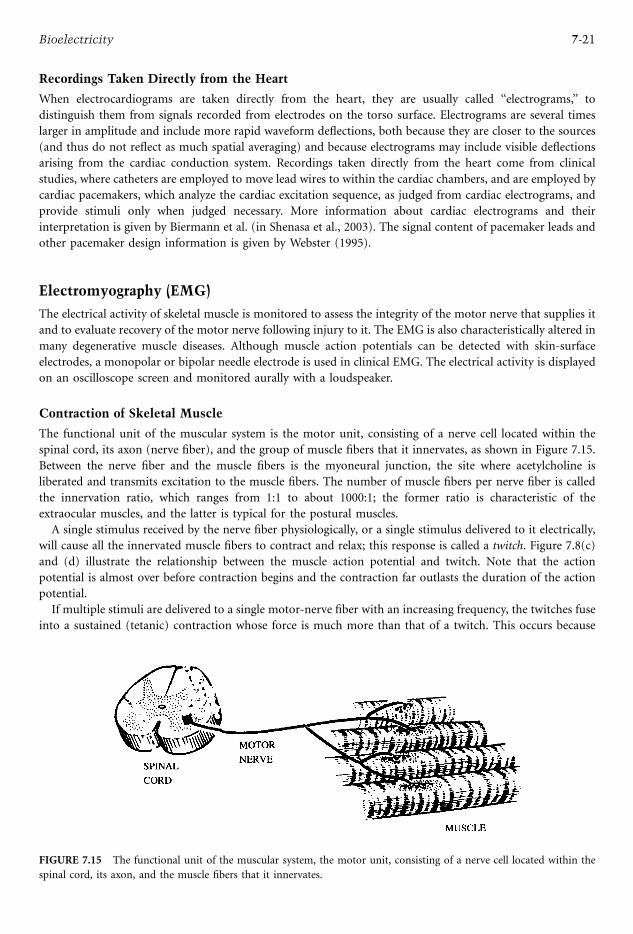
Recordings Taken Directly from the Heart
When electrocardiograms are taken directly from the heart, they are usually called ‘‘electrograms,’’ to
distinguish them from signals recorded from electrodes on the torso surface. Electrograms are several times
larger in amplitude and include more rapid waveform deflections, both because they are closer to the sources
(and thus do not reflect as much spatial averaging) and because electrograms may include visible deflections
arising from the cardiac conduction system. Recordings taken directly from the heart come from clinical
studies, where catheters are employed to move lead wires to within the cardiac chambers, and are employed by
cardiac pacemakers, which analyze the cardiac excitation sequence, as judged from cardiac electrograms, and
provide stimuli only when judged necessary. More information about cardiac electrograms and their
interpretation is given by Biermann et al. (in Shenasa et al., 2003). The signal content of pacemaker leads and
other pacemaker design information is given by Webster (1995).
Electromyography (EMG)
The electrical activity of skeletal muscle is monitored to assess the integrity of the motor nerve that supplies it
and to evaluate recovery of the motor nerve following injury to it. The EMG is also characteristically altered in
many degenerative muscle diseases. Although muscle action potentials can be detected with skin-surface
electrodes, a monopolar or bipolar needle electrode is used in clinical EMG. The electrical activity is displayed
on an oscilloscope screen and monitored aurally with a loudspeaker.
Contraction of Skeletal Muscle
The functional unit of the muscular system is the motor unit, consisting of a nerve cell located within the
spinal cord, its axon (nerve fiber), and the group of muscle fibers that it innervates, as shown in Figure 7.15.
Between the nerve fiber and the muscle fibers is the myoneural junction, the site where acetylcholine is
liberated and transmits excitation to the muscle fibers. The number of muscle fibers per nerve fiber is called
the innervation ratio, which ranges from 1:1 to about 1000:1; the former ratio is characteristic of the
extraocular muscles, and the latter is typical for the postural muscles.
A single stimulus received by the nerve fiber physiologically, or a single stimulus delivered to it electrically,
will cause all the innervated muscle fibers to contract and relax; this response is called a twitch. Figure 7.8(c)
and (d) illustrate the relationship between the muscle action potential and twitch. Note that the action
potential is almost over before contraction begins and the contraction far outlasts the duration of the action
potential.
If multiple stimuli are delivered to a single motor-nerve fiber with an increasing frequency, the twitches fuse
into a sustained (tetanic) contraction whose force is much more than that of a twitch. This occurs because
FIGURE 7.15 The functional unit of the muscular system, the motor unit, consisting of a nerve cell located within the
spinal cord, its axon, and the muscle fibers that it innervates.
7-21Bioelectricity
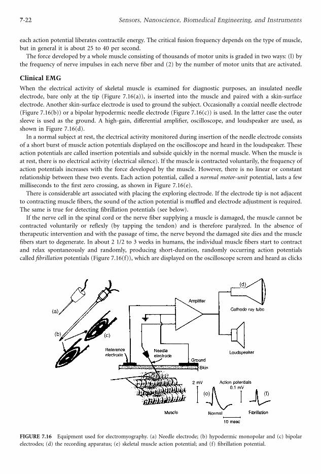
each action potential liberates contractile energy. The critical fusion frequency depends on the type of muscle,
but in general it is about 25 to 40 per second.
The force developed by a whole muscle consisting of thousands of motor units is graded in two ways: (l) by
the frequency of nerve impulses in each nerve fiber and (2) by the number of motor units that are activated.
Clinical EMG
When the electrical activity of skeletal muscle is examined for diagnostic purposes, an insulated needle
electrode, bare only at the tip (Figure 7.16(a)), is inserted into the muscle and paired with a skin-surface
electrode. Another skin-surface electrode is used to ground the subject. Occasionally a coaxial needle electrode
(Figure 7.16(b)) or a bipolar hypodermic needle electrode (Figure 7.16(c)) is used. In the latter case the outer
sleeve is used as the ground. A high-gain, differential amplifier, oscilloscope, and loudspeaker are used, as
shown in Figure 7.16(d).
In a normal subject at rest, the electrical activity monitored during insertion of the needle electrode consists
of a short burst of muscle action potentials displayed on the oscilloscope and heard in the loudspeaker. These
action potentials are called insertion potentials and subside quickly in the normal muscle. When the muscle is
at rest, there is no electrical activity (electrical silence). If the muscle is contracted voluntarily, the frequency of
action potentials increases with the force developed by the muscle. However, there is no linear or constant
relationship between these two events. Each action potential, called a normal motor-unit potential, lasts a few
milliseconds to the first zero crossing, as shown in Figure 7.16(e).
There is considerable art associated with placing the exploring electrode. If the electrode tip is not adjacent
to contracting muscle fibers, the sound of the action potential is muffled and electrode adjustment is required.
The same is true for detecting fibrillation potentials (see below).
If the nerve cell in the spinal cord or the nerve fiber supplying a muscle is damaged, the muscle cannot be
contracted voluntarily or reflexly (by tapping the tendon) and is therefore paralyzed. In the absence of
therapeutic intervention and with the passage of time, the nerve beyond the damaged site dies and the muscle
fibers start to degenerate. In about 2 1/2 to 3 weeks in humans, the individual muscle fibers start to contract
and relax spontaneously and randomly, producing short-duration, randomly occurring action potentials
called fibrillation potentials (Figure 7.16(f)), which are displayed on the oscilloscope screen and heard as clicks
FIGURE 7.16 Equipment used for electromyography. (a) Needle electrode; (b) hypodermic monopolar and (c) bipolar
electrodes; (d) the recording apparatus; (e) skeletal muscle action potential; and (f) fibrillation potential.
7-22 Sensors, Nanoscience, Biomedical Engineering, and Instruments

in the loudspeaker. Although there is electrical activity, the muscle develops no net force. The fibrillation
potentials persist as long as there are viable muscle fibers. In such a denervated muscle, insertion of the needle
electrode elicits a vigorous train of short-duration insertion potentials that resemble fibrillation potentials
with a frequency of about 1 to 10 per second. If the damaged ends of the nerve are brought together surgically,
the central end of the nerve will start to grow slowly and reinnervate the muscle. Gradually, the fibrillation
potentials disappear, although the muscle is still not able to be contracted. Long before there is visible evidence
of muscle contraction, if the subject is presented with the EMG display and asked to contract the affected
muscle, primitive muscle action potentials can be elicited. With the passage of time, the fibrillation potentials
disappear and there is electrical silence at rest and primitive (nascent) motor-unit activity occurs with
voluntary contraction. Later when reinnervation is complete, only normal motor-unit potentials are present
with voluntary contraction and electrical silence at rest.
The EMG is also used to diagnose some degenerative muscle and related nerve disorders. Myotonia is a
degenerative disease of muscle fibers in which the muscle relaxes poorly. Insertion of the needle electrode
elicits an intense burst of insertion potentials that sound like a thunderstorm in the loudspeaker. A similar
response is obtained by tapping the muscle. When relaxation does occur, there is electrical silence. Voluntary
contraction produces normal action potentials along with shorter-duration action potentials from the diseased
muscle fibers.
Myasthenia gravis is a disease in which there is impairment of transmission of acetylcholine across the
myoneural junctions to the muscle fibers. As a result, muscle contraction cannot be sustained. Because the
muscle fibers are normally innervated, there are no fibrillation potentials. With voluntary contraction, normal
action potentials occur, and if the disease is severe, the action potentials decrease in frequency as the force of
contraction decreases and soon sustained muscle contraction cannot be maintained.
Muscular dystrophy is a degenerative disease of muscle fibers in which there is atrophy of some fibers,
swelling in others, and an increase in sarcolemmal and connective tissue with the deposition of fat. Insertion of
the needle electrode elicits a vigorous burst of short-duration, high-frequency action potentials. Typically at
rest there are no fibrillation potentials. With voluntary contraction, the action potentials are short in duration,
high in frequency, and produce a whirring sound in the loudspeaker. As fatigue supervenes, the frequency and
amplitude decrease.
The reader who is interested in obtaining more information on EMG will find it in books by Oh (2003),
Kimura (2001), and Preston and Shapiro (1998). All contain a wealth of clinical information.
Instrumentation
As yet there is no American National Standard for EMG, although steps are being taken in this direction. As
shown in Figure 7.16, the EMG is displayed in two ways: (1) visually with an oscilloscope and (2) aurally with
a loudspeaker. Both are needed to enable acquisition and analysis of the EMG.
Buchtal et al. (1954) stated that the principal frequency components for the human EMG require a
bandwidth of 1 Hz to 10 kHz. It has been found that a time constant of about 50 msec is satisfactory, which
corresponds to a low-frequency –3-dB point of 3 Hz. For needle electrodes with a tip diameter of 0.1 mm or
larger, the input impedance (one side to ground) should not be lower than that of a 500-kO resistor in parallel
with less than 25-pF capacitance.
Smaller-area electrodes require a higher input impedance (Geddes et al., 1967). The cable used to connect
the needle electrode to the amplifier should not add more than 250 pF to the input capacitance. The common-
mode rejection ratio (CMRR) should be in excess of 5000.
Electro-encephalography (EEG)
The electrical activity of the brain can be recorded with electrodes on the scalp, on the exposed brain, or
inserted into the brain. The major advantage of the EEG is its simplicity, while its major limitation is poor
spatial resolution (as evaluated by Purves et al., 1997, p. 500). EEGs are sometimes interpreted in conjunction
with magnetic reasonance imaging (MRI), a recent imaging methodology that provides good spatial
localization (within 1 mm) of active regions of the brain (Purves et al., 1997, p. 22). The EEG has been
7-23Bioelectricity
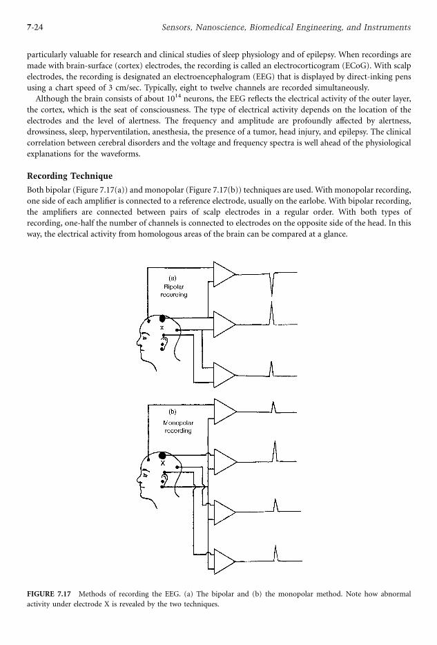
particularly valuable for research and clinical studies of sleep physiology and of epilepsy. When recordings are
made with brain-surface (cortex) electrodes, the recording is called an electrocorticogram (ECoG). With scalp
electrodes, the recording is designated an electroencephalogram (EEG) that is displayed by direct-inking pens
using a chart speed of 3 cm/sec. Typically, eight to twelve channels are recorded simultaneously.
Although the brain consists of about 1014 neurons, the EEG reflects the electrical activity of the outer layer,
the cortex, which is the seat of consciousness. The type of electrical activity depends on the location of the
electrodes and the level of alertness. The frequency and amplitude are profoundly affected by alertness,
drowsiness, sleep, hyperventilation, anesthesia, the presence of a tumor, head injury, and epilepsy. The clinical
correlation between cerebral disorders and the voltage and frequency spectra is well ahead of the physiological
explanations for the waveforms.
Recording Technique
Both bipolar (Figure 7.17(a)) and monopolar (Figure 7.17(b)) techniques are used. With monopolar recording,
one side of each amplifier is connected to a reference electrode, usually on the earlobe. With bipolar recording,
the amplifiers are connected between pairs of scalp electrodes in a regular order. With both types of
recording, one-half the number of channels is connected to electrodes on the opposite side of the head. In this
way, the electrical activity from homologous areas of the brain can be compared at a glance.
FIGURE 7.17 Methods of recording the EEG. (a) The bipolar and (b) the monopolar method. Note how abnormal
activity under electrode X is revealed by the two techniques.
7-24 Sensors, Nanoscience, Biomedical Engineering, and Instruments

With the bipolar method illustrated in Figure 7.17(a), abnormal activity located under electrode X will be
revealed as a phase reversal in adjacent channels. With monopolar recording using the earlobe reference
electrode (Figure 7.17(b)) the abnormal activity under electrode X will be largest in the channel connected to
that electrode and smaller in the adjacent channels.
In clinical EEG, 21 electrodes are applied to the scalp in what is known as the 10-20 system. This array was
established by the International Federation of EEG Societies in 1958. The 10-20 system employs skull
landmarks as reference points to locate the electrodes.
The Normal EEG
In the normal resting adult, the EEG displays a fluctuating electrical activity having a dominant frequency of
about 10 Hz and an amplitude in the range of 20 to 200 mV. This activity is called the alpha rhythm and ranges
in frequency from about 8 to 12 Hz, being most prominent in the occipital and parietal areas. It may occupy
as much as half the record. The alpha rhythm increases in frequency with age from birth and attains its adult
form by about 15 to 20 years. The alpha rhythm is most prominent when the eyes are closed and in the absence
of concentration. Opening the eyes, engaging in patterned vision, or performing such cerebral activity as
mental arithmetic diminishes or abolishes the alpha rhythm. Figure 7.18 presents a good example of this
phenomenon.
Although the alpha rhythm is the most prominent electrical activity, other frequencies are present. For
example, there is a considerable amount of low-voltage, high-frequency (beta) activity ranging from 18 to
30 Hz. It is usually found in the frontal part of the brain. However, the normal electroencephalogram contains
waves of various frequencies (in the range of 1 to 60 Hz) and amplitudes, depending on the cerebral state. To
establish communication among electroencephalographers, a terminology has been developed to describe
waveforms and their frequencies; Table 7.1 presents a glossary of these terms.
Drowsiness and sleep affect the normal EEG profoundly. Figure 7.19 illustrates the typical changes that
occur as a subject goes to sleep. With drowsiness, the higher-frequency activity which is associated with
alertness or excitement, and the alpha rhythm that dominates the waking record in the relaxed state, are
replaced by a characteristic cyclic sequence of changes which constitute the focus of a new specialty devoted to
sleep physiology, in which the EEG is used to identify different stages of sleep.
TABLE 7.1 EEG Waveform Terminology
Waveform Frequency (Hz) Conditions
Alpha 8–12 Parietal-occipital, associated with the awake and relaxed subject, prominent
with eyes closed
Beta 18–30 More evident in frontal-parietal leads, seen best when alpha is blocked
Delta 1–3.5 Associated with normal sleep and present in children less than 1 year old, also
seen in organic brain disease
Theta 4–7 Parietal-temporal, prominent in children 2 to 5 years old
Sleep spindle (sigma) 12–14 Waxing and waning of a sinusoidal-like wave having the envelope that resembles
a spindle, seen during sleep
Lambda Transient Visually evoked, low-amplitude, occipital wave, resulting from recognition of a
new visual image
Spike and wave ca. 3 Sharp wave (spike) followed by rounded wave associated with petit mal epilepsy
FIGURE 7.18 The EEG of a relaxed human subject with eyes closed and open. Note that the record is dominated with
alpha rhythm (8 to 12 Hz) when the eyes are closed. (Source: Derived in part from M.A.B. Brazier, The Electrical Activity of
the Nervous System, London: Sir Isaac Pitman & Sons, Ltd., 1951. With permission.)
7-25Bioelectricity

Rapid, deep breathing (hyperventilation) at a rate of 30 per minute for about 3 min reduces the partial
pressure of carbon dioxide in the blood, which reduces cerebral blood flow. A typical EEG response consists of
large-amplitude, bilaterally synchronous, frontally prominent waves with a frequency of 4 to 7 per second. The
frequency usually decreases with increasing hyperventilation. The lack of bilateral symmetry is an indication of
abnormality.
Anesthesia dramatically alters the EEG in a manner that depends on the type and amount of anesthetic
given. Despite differences among anesthetic agents, some important similarities accompany anesthesia. The
first change is replacement of the alpha rhythm with low-voltage, high-frequency activity that accompanies the
analgesia and delirium stages. Thus, the EEG resembles that of an alert or excited subject, although the subject
is not appropriately responsive to stimuli; usually the response is excessive and/or inappropriate. From this
point on, the type of EEG obtained with deepening anesthesia depends on the type of anesthetic. However,
when a deeper level of anesthesia is reached, the EEG waveform becomes less dependent on the type of
anesthetic. Large-amplitude low-frequency waves begin to dominate the record, and with deepening
anesthesia their frequency is reduced and they begin to occur intermittently. With very (dangerously) deep
anesthesia, the record is flat (i.e., isoelectric). Complicating interpretation of the EEG in anesthesia are the
effects of hypoxia, hypercapnia, and hypoglycemia, all of which mimic deep anesthesia.
Clinical EEG
The EEG plays a valuable role in identifying intracranial pathology. The clinical utility relies on recognition of
patterns of frequency, voltage, and waveform. Localization of abnormal areas is provided by the multiple scalp
electrodes and recording channels.
The EEG has its greatest value as an aid in the diagnosis and differentiation of the many types of epilepsy,
a condition in which groups of neurons in the brain become hyperexcitable and, depending on their
location, produce sensory, motor, and/or autonomic manifestations. The epilepsies associated with cortical
lesions are often detected by the scalp EEG. The EEG in epileptics is usually abnormal between, as well as
during, attacks. The EEG provides information on the location of the area (or areas) of abnormal neuronal
activity.
Petit mal epilepsy is characterized by a transient loss (few to 20 sec) of conscious thought, although motor
activity may continue. Often there are eye movements and blinking. The EEG shows a characteristic 3 per
second spike-and-wave pattern (Figure 7.20(a)). Psychomotor epilepsy is characterized by sensory
hallucinations and abnormal thoughts, often with stereotyped behavior. During the attack, the subject is
stuporous and the EEG (Figure 7.20(b)) has a characteristic pattern. Jacksonian, or motor, epilepsy starts in a
specific area of the motor cortex and is preceded by an aura, a characteristic sensation perceived by the subject.
FIGURE 7.19 The EEG of a subject going to sleep. (Source: H. Jasper, in Epilepsy and Cerebral Localization, W.G. Penfield
and T.C. Erickson, Eds., Springfield, IL: Charles C Thomas, 1941. With permission.)
7-26 Sensors, Nanoscience, Biomedical Engineering, and Instruments
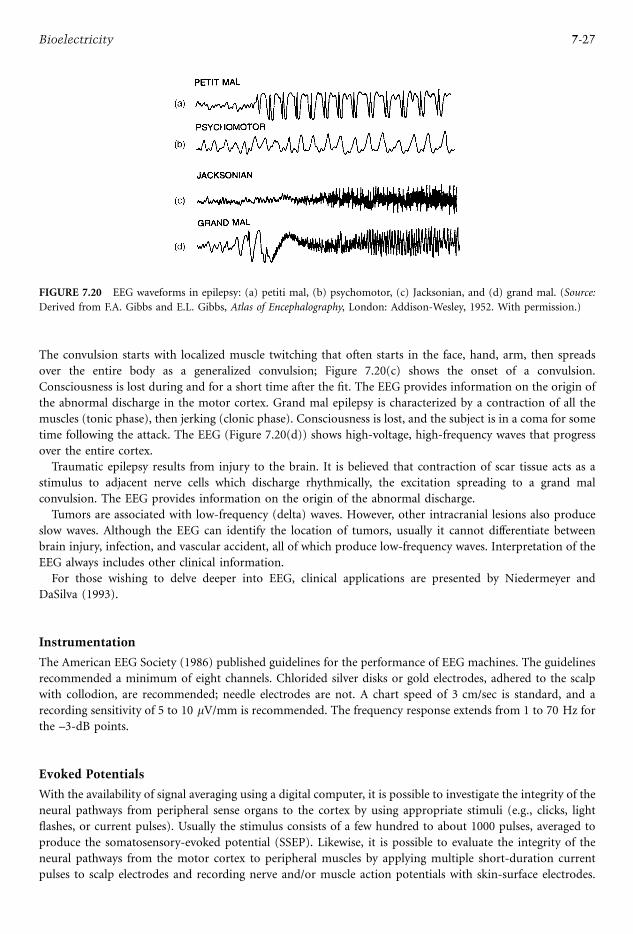
The convulsion starts with localized muscle twitching that often starts in the face, hand, arm, then spreads
over the entire body as a generalized convulsion; Figure 7.20(c) shows the onset of a convulsion.
Consciousness is lost during and for a short time after the fit. The EEG provides information on the origin of
the abnormal discharge in the motor cortex. Grand mal epilepsy is characterized by a contraction of all the
muscles (tonic phase), then jerking (clonic phase). Consciousness is lost, and the subject is in a coma for some
time following the attack. The EEG (Figure 7.20(d)) shows high-voltage, high-frequency waves that progress
over the entire cortex.
Traumatic epilepsy results from injury to the brain. It is believed that contraction of scar tissue acts as a
stimulus to adjacent nerve cells which discharge rhythmically, the excitation spreading to a grand mal
convulsion. The EEG provides information on the origin of the abnormal discharge.
Tumors are associated with low-frequency (delta) waves. However, other intracranial lesions also produce
slow waves. Although the EEG can identify the location of tumors, usually it cannot differentiate between
brain injury, infection, and vascular accident, all of which produce low-frequency waves. Interpretation of the
EEG always includes other clinical information.
For those wishing to delve deeper into EEG, clinical applications are presented by Niedermeyer and
DaSilva (1993).
Instrumentation
The American EEG Society (1986) published guidelines for the performance of EEG machines. The guidelines
recommended a minimum of eight channels. Chlorided silver disks or gold electrodes, adhered to the scalp
with collodion, are recommended; needle electrodes are not. A chart speed of 3 cm/sec is standard, and a
recording sensitivity of 5 to 10 mV/mm is recommended. The frequency response extends from 1 to 70 Hz for
the –3-dB points.
Evoked Potentials
With the availability of signal averaging using a digital computer, it is possible to investigate the integrity of the
neural pathways from peripheral sense organs to the cortex by using appropriate stimuli (e.g., clicks, light
flashes, or current pulses). Usually the stimulus consists of a few hundred to about 1000 pulses, averaged to
produce the somatosensory-evoked potential (SSEP). Likewise, it is possible to evaluate the integrity of the
neural pathways from the motor cortex to peripheral muscles by applying multiple short-duration current
pulses to scalp electrodes and recording nerve and/or muscle action potentials with skin-surface electrodes.
FIGURE 7.20 EEG waveforms in epilepsy: (a) petiti mal, (b) psychomotor, (c) Jacksonian, and (d) grand mal. (Source:
Derived from F.A. Gibbs and E.L. Gibbs, Atlas of Encephalography, London: Addison-Wesley, 1952. With permission.)
7-27Bioelectricity
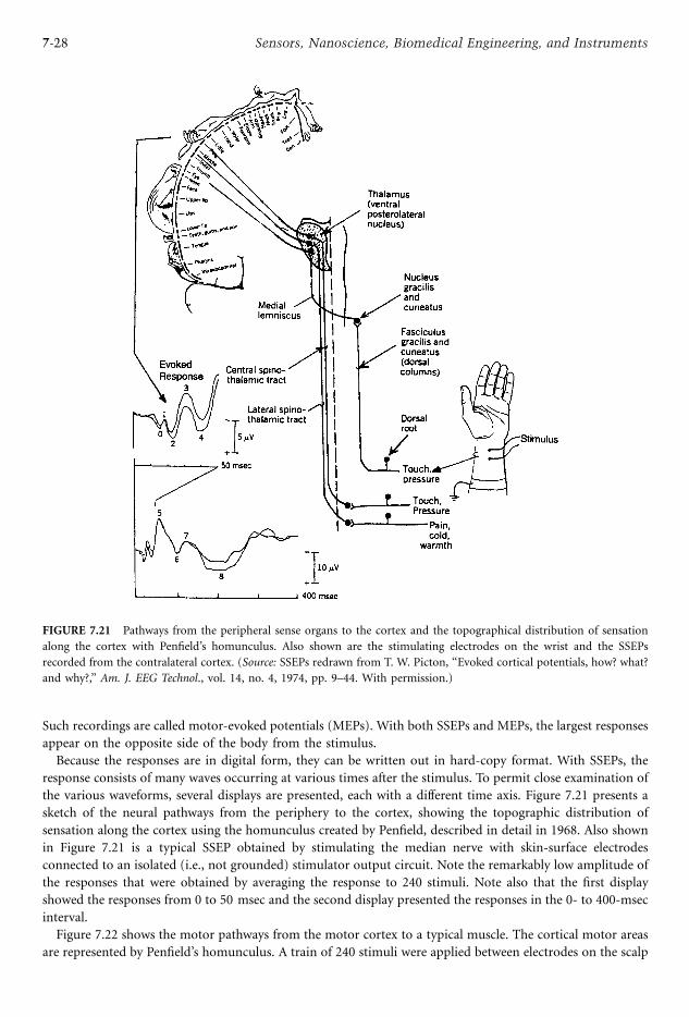
Such recordings are called motor-evoked potentials (MEPs). With both SSEPs and MEPs, the largest responses
appear on the opposite side of the body from the stimulus.
Because the responses are in digital form, they can be written out in hard-copy format. With SSEPs, the
response consists of many waves occurring at various times after the stimulus. To permit close examination of
the various waveforms, several displays are presented, each with a different time axis. Figure 7.21 presents a
sketch of the neural pathways from the periphery to the cortex, showing the topographic distribution of
sensation along the cortex using the homunculus created by Penfield, described in detail in 1968. Also shown
in Figure 7.21 is a typical SSEP obtained by stimulating the median nerve with skin-surface electrodes
connected to an isolated (i.e., not grounded) stimulator output circuit. Note the remarkably low amplitude of
the responses that were obtained by averaging the response to 240 stimuli. Note also that the first display
showed the responses from 0 to 50 msec and the second display presented the responses in the 0- to 400-msec
interval.
Figure 7.22 shows the motor pathways from the motor cortex to a typical muscle. The cortical motor areas
are represented by Penfield’s homunculus. A train of 240 stimuli were applied between electrodes on the scalp
FIGURE 7.21 Pathways from the peripheral sense organs to the cortex and the topographical distribution of sensation
along the cortex with Penfield’s homunculus. Also shown are the stimulating electrodes on the wrist and the SSEPs
recorded from the contralateral cortex. (Source: SSEPs redrawn from T. W. Picton, ‘‘Evoked cortical potentials, how? what?
and why?,’’ Am. J. EEG Technol., vol. 14, no. 4, 1974, pp. 9–44. With permission.)
7-28 Sensors, Nanoscience, Biomedical Engineering, and Instruments
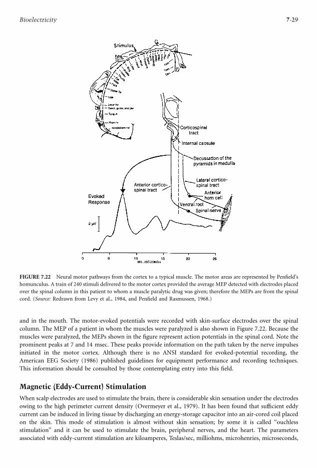
and in the mouth. The motor-evoked potentials were recorded with skin-surface electrodes over the spinal
column. The MEP of a patient in whom the muscles were paralyzed is also shown in Figure 7.22. Because the
muscles were paralyzed, the MEPs shown in the figure represent action potentials in the spinal cord. Note the
prominent peaks at 7 and 14 msec. These peaks provide information on the path taken by the nerve impulses
initiated in the motor cortex. Although there is no ANSI standard for evoked-potential recording, the
American EEG Society (1986) published guidelines for equipment performance and recording techniques.
This information should be consulted by those contemplating entry into this field.
Magnetic (Eddy-Current) Stimulation
When scalp electrodes are used to stimulate the brain, there is considerable skin sensation under the electrodes
owing to the high perimeter current density (Overmeyer et al., 1979). It has been found that sufficient eddy
current can be induced in living tissue by discharging an energy-storage capacitor into an air-cored coil placed
on the skin. This mode of stimulation is almost without skin sensation; by some it is called ‘‘ouchless
stimulation’’ and it can be used to stimulate the brain, peripheral nerves, and the heart. The parameters
associated with eddy-current stimulation are kiloamperes, Teslas/sec, milliohms, microhenries, microseconds,
FIGURE 7.22 Neural motor pathways from the cortex to a typical muscle. The motor areas are represented by Penfield’s
homunculus. A train of 240 stimuli delivered to the motor cortex provided the average MEP detected with electrodes placed
over the spinal column in this patient to whom a muscle paralytic drug was given; therefore the MEPs are from the spinal
cord. (Source: Redrawn from Levy et al., 1984, and Penfield and Rasmussen, 1968.)
7-29Bioelectricity
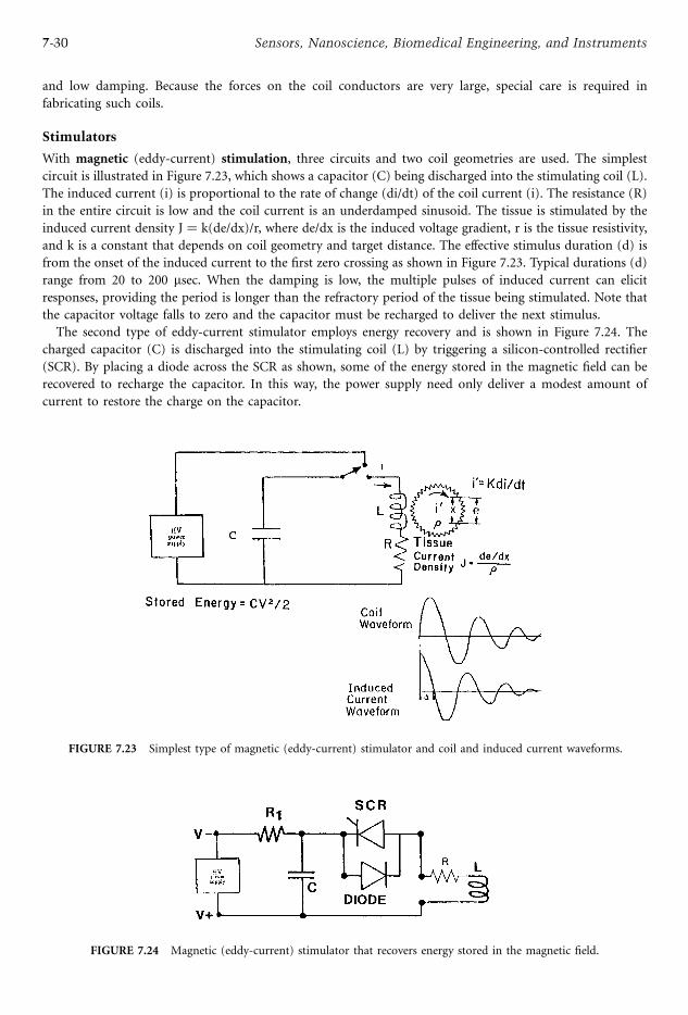
and low damping. Because the forces on the coil conductors are very large, special care is required in
fabricating such coils.
Stimulators
With magnetic (eddy-current) stimulation, three circuits and two coil geometries are used. The simplest
circuit is illustrated in Figure 7.23, which shows a capacitor (C) being discharged into the stimulating coil (L).
The induced current (i) is proportional to the rate of change (di/dt) of the coil current (i). The resistance (R)
in the entire circuit is low and the coil current is an underdamped sinusoid. The tissue is stimulated by the
induced current density J ¼ k(de/dx)/r, where de/dx is the induced voltage gradient, r is the tissue resistivity,
and k is a constant that depends on coil geometry and target distance. The effective stimulus duration (d) is
from the onset of the induced current to the first zero crossing as shown in Figure 7.23. Typical durations (d)
range from 20 to 200 msec. When the damping is low, the multiple pulses of induced current can elicit
responses, providing the period is longer than the refractory period of the tissue being stimulated. Note that
the capacitor voltage falls to zero and the capacitor must be recharged to deliver the next stimulus.
The second type of eddy-current stimulator employs energy recovery and is shown in Figure 7.24. The
charged capacitor (C) is discharged into the stimulating coil (L) by triggering a silicon-controlled rectifier
(SCR). By placing a diode across the SCR as shown, some of the energy stored in the magnetic field can be
recovered to recharge the capacitor. In this way, the power supply need only deliver a modest amount of
current to restore the charge on the capacitor.
FIGURE 7.23 Simplest type of magnetic (eddy-current) stimulator and coil and induced current waveforms.
FIGURE 7.24 Magnetic (eddy-current) stimulator that recovers energy stored in the magnetic field.
7-30 Sensors, Nanoscience, Biomedical Engineering, and Instruments
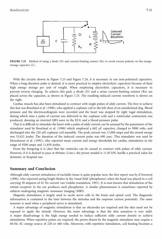
With the circuits shown in Figure 7.23 and Figure 7.24, it is necessary to use non-polarized capacitors.
When a long-duration pulse is desired, it is more practical to employ electrolytic capacitors because of their
high energy storage per unit of weight. When employing electrolytic capacitors, it is necessary to
prevent reverse charging. To achieve this goal, a diode (D) and a series current-limiting resistor (Rz) are
placed across the capacitor, as shown in Figure 7.25. The resulting induced current waveform is shown on
the right.
Cardiac muscle has also been stimulated to contract with single pulses of eddy current. The first to achieve
this feat was Bourland et al. (1990), who applied a coplanar coil to the left chest of an anesthetized dog. Blood
pressure and the electrocardiogram were recorded and the heart was stopped by right vagal stimulation,
during which time a pulse of current was delivered to the coplanar coils and a ventricular contraction was
produced, showing an inverted QRS wave in the ECG and a blood-pressure pulse.
That it is difficult to stimulate the heart with a pulse of eddy current can be assessed by the parameters of the
stimulator used by Bourland et al. (1990) which employed a 682 mF capacitor, charged to 9900 volts, and
discharged into the 220 mH coplanar coil assembly. The peak current was 17,000 amps and the stored energy
was 33,421 joules. The duration of the induced current pulse was 690 msec. This stimulator was used by
Mouchawar et al. (1992), who reported mean current and energy thresholds for cardiac stimulation in the
range of 9200 amps and 11,850 joules.
From the foregoing it is clear that the ventricles can be caused to contract with pulses of eddy current.
However, if it is desired to pace at 60/min (1/sec), the power needed is 11.85 kW, hardly a practical value for
domestic or hospital use.
Summary and Conclusion
Although eddy-current stimulation of excitable tissue is quite popular now, the first report was by d’Arsonval
(1896), who reported seeing bright flashes in the visual field (phosphenes) when the head was placed in a coil
carrying 30 amperes of 42 Hz current (see Geddes translation, 1991). It is now known that stimulation of the
retinal receptors in the eye produces such phosphenes. A similar phenomenon is sometimes reported by
subjects undergoing magnetic resonance imaging (MRI).
Magnetic stimulation is largely used to excite nerve cells in the brain and spinal cord. The diagnostic
information is contained in the time between the stimulus and the response (action potential). The same
measure is used when a peripheral nerve is stimulated.
A major advantage of magnetic stimulation is that no electrodes are required and the skin need not be
exposed to apply the stimuli. However, the main advantage is that the skin sensation is very mild.
A major disadvantage is the high energy needed to induce sufficient eddy current density to achieve
stimulation. When repetitive pulses are required, the power drawn by the magnetic stimulator may require a
60-Hz AC energy source of 220 or 440 volts. Moreover, with repetitive stimulation, coil heating becomes a
FIGURE 7.25 Method of using a diode (D) and current-limiting resistor (Rz) to avoid reverse polarity on the energy-
storage capacitor (C).
7-31Bioelectricity

problem. The availability of magnetically permeable materials that saturate at several orders of
magnitude above presently available materials would be of benefit to the field of magnetic (eddy-current)
stimulation.
This section has focused only on the three most prominent bioelectric events, those of the heart, skeletal
muscle, and brain. The eye, ear, sweat glands, and many types of smooth muscle produce action potentials
that are used for their diagnostic value, as well as being the subject of ongoing research. The
reader interested in delving deeper into this field can find such information in a book by Geddes and
Baker (1989).
Defining Terms
Atrophy: Wasting of cells deprived of nourishment.
Autonomic: That part of the nervous system that controls the internal organs.
Ectopic beat: A heart beat that originates from other than the normal site.
Hypocapnia: A condition of reduced carbon dioxide in the blood.
Hypoxia: A reduced amount of oxygen.
Magnetic stimulation: Eddy-current stimulation.
Metabolic process: The method by which cells use oxygen and produce carbon dioxide and heat.
Myocardial infarction: A heart attack in which a region of the heart muscle is deprived of blood and
soon dies.
Occipital: The back of the brain.
Parietal: The side of the brain.
References
American EEG Society, ‘‘Guidelines in EEG and evoked potentials,’’ Am. J. Clin. Neurophysiol., 3, Suppl., 1986.
Association for the Advancement of Medical Instrumentation (AAMI), Diagnostic ECG Devices, ANSI-AAMI
Standard EC-101-1991.
J.D. Bourland, G.A. Mouchawar, J.A. Nyenhuis, et al., ‘‘Transchest magnetic (eddy-current) stimulation of the
dog heart,’’ Med. Eng. Comput., March, pp. 196–198, 1990.
F. Buchtal, C. Guld, and P. Rosenflack, ‘‘Action potential parameters of normal human muscle and their
dependence on physical variables,’’ Acta Physiol. Scand., 32, pp. 200–220, 1954.
T-C. Chou, Electrocardiography in Clinical Practice, 3rd ed., Philadelphia, PA: W.B. Saunders, 1991.
H.L. Cohen and F. Brumlik,Manual of Electromyography, New York: Hoeber Medical Division, Harper & Row,
1969.
A. d’Arsonval, ‘‘Dispositifs pour la mesure des courants alternatifs de toutes frequences,’’ C.R. Soc. Biol. (Paris),
2, pp. 450–451, 1896.
L.A. Geddes, ‘‘The history of magnetic stimulation,’’ J. Neurophysiol., vol. 8, no. 1, pp. 3–9, 1991.
L.A. Geddes, L.E. Baker, and M. McGoodwin, ‘‘The relationship between electrode area and amplifier
input impedance in recording muscle action potentials,’’ Med. Biol. Eng. Comput., vol. 5, pp. 561–568,
1967.
L.A. Geddes and L.E. Baker, Principles of Applied Biomedical Instrumentations, 3rd ed., New York: Wiley,
1989.
J. Kimura, Electrodiagnosis in Diseases of Nerve and Muscle: Principles and Practice, Oxford: Oxford University
Press, 2001.
A.G. Kleber and Y. Rudy, ‘‘Basic mechanisms of cardiac impulse propagation and associated arrhythmias,’’
Physiol. Rev., 84, pp. 431–488, 2004.
International Federation of EEG Societies, J. Knott, Chairman, EEG Clin. Neurophysiol., 10, pp. 378–380, 1958.
International Federation for Electroencephalography and Clinical Neurophysiology, EEG. Clin. Neurophysiol.,
10, pp. 371–375, 1958.
7-32 Sensors, Nanoscience, Biomedical Engineering, and Instruments
W.J. Levy, D.H. York, M. McCaffery, and F. Tanzer, ‘‘Evoked potentials from transcranial stimulation of the
motor cortex in humans,’’ Neurosurgery, vol. 15, no. 3, pp. 287–302, 1983.
G.A. Mouchawar, J.D. Bourland, and J.A. Nyenhuis et al., ‘‘Closed-chest cardiac stimulation with a pulsed
magnetic field,’’ Med. Biol. Eng. Comput., March, pp. 162–168, 1992.
S. Nelson, D.B. Geselowitz, and C.V. Nelson, The Theoretical Basis of Electrocardiology, Oxford: Oxford
University Press, 1985.
E. Niedermeyer and F. L. DaSilva, Electroencephalography, Basic Principles, Clinical Applications, and Related
Fields, Baltimore, MD: Williams & Wilkins, 1993.
S.J. Oh, Clinical Electromyography: Nerve Conduction Studies, Philadelphia, PA: Lippincott Williams & Wilkins,
2003.
K.M. Overmeyer, J.A. Pearce, and D.P. DeWitt, ‘‘Measurement of temperature distributions at electrosurgical
dispersive electrode sites,’’ Trans. ASME, J. Biomech. Eng., 101, pp. 66–72, 1979.
W. Penfield and T. Rasmussen, The Cerebral Cortex of Man, New York: Hafner, 1968.
R.E. Phillips and M.K. Feeney, The Cardiac Rhythms: A Systematic Approach to Interpretation, 3rd ed.,
Philadelphia, PA: W.B. Saunders, 1990.
T.W. Picton, ‘‘Evoked cortical potentials, how? what? and why?,’’ Am. J. EEG Technol., vol. 14, no. 4, pp. 9–44,
1974.
D.C. Preston and B. E. Shapiro, Electromyography and Neuromuscular Disorders: Clinical-Electrophysiologic
Correlations, London: Butterworth–Heinemann, 1998.
D. Purves, G.J. Augustine, D. Fitzpatrick, L.C. Katz, A.S. LaMantia, and J.O. McNamara, Neuroscience,
Sunderland, MA: Sinauer Associates, Inc. 1997
M. Shenasa, M. Borggrefe, and G. Breithardt, Eds., Cardiac Mapping, 2nd ed., Mount Kisco, NY: Futura Pub.
Co., 2003.
J. Webster, Ed., Design of Cardiac Pacemakers, New York: IEEE Press, 1995.
7.3 Biological Effects and Electromagnetic Fields
Bonnie Keillor Slaten and Frank Barnes
Introduction
The purpose of this section is to provide the electrical professional with information on the biological
effects of electric and magnetic fields at levels ranging from those that result in shock, to the low-level time-
varying electromagnetic fields (EMF) from power lines. Additionally, we will review some of the current
data on biological effects, at higher frequencies, from cell phones and base stations. The effects of electric
shock are probably the best understood and a cause–effect relationship has been established. The biological
effects of EMF from power lines, cell phones, and base stations to a population are more problematic, as a
cause–effect relationship has not been established for these exposures. Intermediate levels have shown
therapeutic effects for the repair of broken bones and modifications of cell growth rates. The potential of
biological effects of EMF from power lines, cell phones, and base stations has been in the public eye and has
become quite controversial. The data on health effects continues to be inconclusive, and the setting of
standards reflects the differing philosophies with respect to incomplete understanding of the thresholds and
nature of the biological effect of EMF. This section attempts to provide some of the background on these
controversies.
The first subsection discusses the biological effects of electric shock. The second subsection is a discussion of
the biological effects of EMF from power lines. A short discussion of exposure is presented and a review of the
epidemiological studies follows. Reviews of animal and cellular studies of EMF from power lines are also
presented. The third subsection is a discussion of the biological effects of EMF from cell phones and base
stations. Exposure is discussed, followed by a review of epidemiological and cellular studies. Standards and
guidelines are presented, as well as a discussion on risk.
7-33Bioelectricity

Biological Effects of Electric Shock
The biological effects of an electrical shock are a function of the duration, magnitude, frequency, and path of
the current passing through the body, as well as skin moisture. Electric current damages the body in three
different ways:
1. It harms or interferes with proper functioning of the nervous system and heart.
2. It subjects the body to intense heat.
3. It causes the muscles to contract.
The nervous system is an electrical network that uses extremely low currents. Even very low-current electric
shock can disrupt the normal functioning of muscles—most significantly, the heart. Electric shock also
produces violent muscle contractions, which is why a person receiving a shock is frequently unable to ‘‘let go.’’
It may also cause the heart to lose its coordination or rhythm. Even currents that produce no noticeable
heating of tissue or visible injury can cause these effects (Jefferson Lab, 2004).
Electrical shock can also produce rapid and destructive heating of body tissue. Seemingly minor external
effects (specifically burns) may be indicative of much more extensive internal injury and there can potentially
be delayed effects.
Alternating current (ac) is more dangerous than direct current (dc), and 60-cycle current is more dangerous
than high-frequency current. ac is said to be four to five times more dangerous than dc because ac causes more
severe muscular contraction. In addition, ac stimulates sweating that lowers the skin resistance. Humans and
animals are most susceptible to frequencies at 50 to 60 Hz because the internal frequency of the nerve signals
controlling the heart is approximately 60 Hz (Electric Shock Precautions, 2004).
The National Electrical Code (NEC) in the United States considers 5 mA (0.005 amps) to be a safe upper
limit for children and adults; hence the 5-mA Ground Fault Interrupter (GFI) circuit breaker requirement for
wet locations (Bass Associates, 2004). The values in Table 7.2 should be used as a guide instead of absolute data
points. For instance, 99% of the female population have a ‘‘let go’’ limit above 6 mA, with an average of
10.5 mA; while 99% of the male population have a ‘‘let go’’ above 9 mA, with an average of 15.5 mA (Bass
Associates, 2004).
Ventricular fibrillation can occur at current levels as low as 30 mA for a 2-year-old child and 60 mA for
adults. Most adults will go into ventricular fibrillation at hand-to-hand currents below 100 mA (0.1 amp)
(Bass Associates, 2004).
Typically, if touching a 120-V circuit with one hand, a person can escape serious shock if he has insulating
shoes that prevent a low-resistance path to ground. This fact has led to the common ‘‘hand in the pocket’’
practice for engineers and electrical workers. If they keep one hand in their pocket when touching a circuit,
they are less likely to have the kind of path to ground that will result in a serious shock (Nave and Nave, 1985).
TABLE 7.2 Physiological Effects of Shock
Electric Current
(1 sec contact) Physiological Effect
Voltage Required to Produce
the Current with Assumed
Body Resistance
100,000 O 1,000 O1 mA Threshold of feeling, tingling sensation 100 V 1 V
5 mA Accepted as maximum harmless current 500 V 5 V
10–20 mA Beginning of sustained muscular contraction
(‘‘can’t let go’’ current)
1,000 V 10 V
100–300 mA Ventricular fibrillation, fatal if continued
Respiratory function continues
10,000 V 100 V
6 A Sustained ventricular contraction followed
by normal heart rhythm (defibrillation)
Temporary respiratory paralysis and
possibly burns
600,000 V 6,000 V
Source: C.R. Nave and B.C. Nave, Physics for the Health Sciences, 3rd ed., Philadelphia: W.B. Saunders, 1985.
7-34 Sensors, Nanoscience, Biomedical Engineering, and Instruments
Will the 120-V Common Household Voltage Produce a DangerousShock? It Depends!
If your body resistance is 100,000 O, then the current which would flow would be:
I ¼ 120V
100; 000O¼ 0:0012A ¼ 1:2mA
This is just about at the threshold of perception, so it would only produce a tingle.
If you had just played a couple of sets of tennis, and were sweaty and barefoot, then the resistance to ground
might be as low as 1,000 O. Then the current would be:
I ¼ 120V
1000O¼ 0:12A ¼ 120mA
This is a lethal shock, capable of producing ventricular fibrillation and death! The severity of shock from a
given source will depend upon its path through the body (Nave and Nave, 1985).
Table 7.3 shows some of the typical human body resistances to electrical current. Barring broken skin,
body-circuit resistance, even in contact with liquid, will probably be not less than 500 O. However, the currentflow at this resistance and 120 V is 240 mA—over twice that required to cause death (Jefferson Lab, 2004).
The path through the body has much to do with the shock danger. A current passing from finger to elbow
through the arm may produce only a painful shock, but that same current passing from hand to hand or from
hand to foot may well be fatal.
A burn from electrocution is much different than a burn from scalding or fire. Fleshy tissue is destroyed at
122–F and the vascular tissue serving the nerves suffers damage at considerably lower temperatures. Victims ofindustrial high-voltage accidents will display obvious thermal destruction at the skin contact points. The
extremities may be slightly swollen but otherwise without visible surface damage. Yet beneath the involved skin,
the skeletal muscle will often be in a state of severe unrelenting spasm or rigor. There will frequently be marked
sensory and motor nerve malfunction. Within the first week after injury, many victims will undergo sequential
surgical procedures to remove damaged nonviable skeletal muscle, resulting in a weak, stiff extremity that is
often anesthetic because of nerve damage, and cold because of poor circulation. Under these circumstances,
the patient is better off undergoing amputation and then receiving a prosthetic extremity (R. Lee, 1991).
In general, muscle and nerve appear to be the tissues with the greatest vulnerability to injury by electrical
current. There is a characteristic skeletal muscle tissue injury pattern in victims of high-voltage electrical shock
that is relatively unique to shock victims. Muscle adjacent to the bone and joints is recognized clinically to be
the most vulnerable to electrical trauma. In addition, muscle cells located in the central region of the muscle
may also be vulnerable and nerves seem to have a lower threshold for damage than muscle (R. Lee, 1991).
In conclusion, if the contact to the source of the shock is brief, nonthermal mechanisms of cell damage may
be most important. If the contact is much longer, heat damage will be most destructive and if heat damage
predominates, then the injury may not be limited just to the plasma membrane but to other cell membranes as
well, and this is unlikely to be reversible (R. Lee, 1991).
TABLE 7.3 Typical Human Body Resistance to Electrical
Current
Body Area Resistance (O)
Dry skin 100,000–600,000
Wet skin 1,000
Internal body (hand to foot) 400–600
Ear to ear ,100
Source: C.R. Nave and B.C. Nave, Physics for the Health Sciences,3rd ed., Philadelphia: W.B. Saunders, 1985.
7-35Bioelectricity

Other Adverse Effects of Electricity
Electrical Arc Flash
When an electrical arc occurs, it can produce temperatures up to 35,000–F. This melts and vaporizes the
constituents of the conductor, rapidly heating the surrounding air—with potentially explosive force.
One cubic inch of copper, for example, produces 1.44 cubic yards of vapor. This is comparable to the
expansion rate of dynamite. Electrical explosions can be fatal within 10 ft of the arc, and can cause burns up to
40 ft away (Jefferson Lab, 2004).
Biological Effects of Low-Level, Time-Varying ElectromagneticFields (EMF) from Power Lines
The effects of electric fields on biological systems have been studied since the discovery of electricity,
and electricity has been used to treat a wide variety of illnesses including depression and broken bones. It is
relatively recently that the general population has become concerned that weak magnetic fields, those that are
less than a tenth of the Earth’s magnetic field, may cause adverse biological effects. The possibility that the time
varying magnetic field from power lines might be associated with the incidence of childhood cancer was first
raised by Wertheimer in an epidemiological study in 1979 (Wertheimer et al., 1995). Since that time a large
number of studies have been carried out and more than 37,000 papers written on the biological effects of
electric and magnetic fields. The results of many of these studies are controversial for a number of reasons; the
primary reason being the inability to establish a cause–effect relationship at the weak field levels that are
generally associated with exposures from power lines.
It is well established that there are biological effects of electric and magnetic fields at high levels of exposure.
As presented earlier, currents at lower levels, of the order of 10 mA, are large enough to produce an electric
shock. Current densities of microamperes per centimeter squared are about the same intensity as the currents
that flow naturally in the human body and are large enough to modify growth processes. The current densities
that are typically induced by the time-varying fields from power lines that are in the range from 0.1 to 10 mT(1 to 100 mG) at 60 Hz are estimated to result in current densities significantly less than 0.04 mA cm–2. As
these currents are considerably smaller than the naturally flowing currents in the human body, it is not clear
whether or not they are biologically significant. Biological systems are typically highly nonlinear and have
thresholds. Thus, a small current injected into the heart’s natural pacemaker cell may have little or no effect on
its firing rate, whereas a current of the same intensity at a different time or one that is two or three times larger
may either stop the firing altogether or speed it up. The biological effect of the current depends on the
direction of the current and when it is applied during the cell’s firing cycle.
Additionally, biological systems have a large number of feedback loops that tend to cancel out undesirable
changes. Thus, one can have changes in a biological system as a result of small currents or small concentrations of
chemicals that are corrected by the body and do not result in adverse health effects. For example, exercise may
dissipate four or five times as much metabolic energy as rest. This could be expected to raise the body
temperature. However, the result of such exercise causes you to sweat and your body temperature remains nearly
constant. Tomake things evenmore complex, some effects like stress can be either positive or negative depending
on the circumstances and past history. Stress reactions like the release of heat shock proteins can protect the body
against elevated temperature; however, prolonged stress can deplete the body’s ability to respond a new stress.
The net result of these complexities is that the scientific community is not in a position to say that any given
exposure level is safe. However, it is equally true that data are not available to say that the magnetic fields in the
ranges that are associated with power lines are harmful.
Exposures
Both electric and magnetic fields are associated with power lines. The electric fields are proportional to the
voltage and typically decrease rapidly with distance. The voltage rating on power lines in Colorado, ranges
from 340 kV to 110 V to ground and 220 V between lines into the house (Thompson, 2003). These electric
fields are relatively easy to reduce by metal shields from the typical values of 5 to 10 kV m–1 under power lines
7-36 Sensors, Nanoscience, Biomedical Engineering, and Instruments

to levels less than 100 to 200 V m–1, which is typical for peak values in normal households. Average values for
electric fields in houses are typically about 10 V m–1.
Themagnetic fields are proportional to the current flowing in thewires and also decrease rapidly with distance.
The intensity of these fields at a distance typically increaseswith the spacing between thewires anddecreases as the
distance from the wires increases at a rate that is greater than one over the distance cubed (1 D–3). It should be
noted that currents flowing in low-voltage lines, and thus the magnetic fields, might be as large as those in high-
voltage lines. However, transmission lines tend to have higher average currents as the power is delivered to awide
variety of customers with peak power demands at different times. As the required power increases, the power
companies typically raise the voltage in order to reduce the losses in the transmission lines that are proportional to
the square of the current. It often occurs thatwhen the transmission lines are upgraded and the voltages are raised,
the currents and the magnetic fields are reduced.
Burying the transmission lines primarily means that the lines are out of sight. The fields typically decrease
more rapidly with distance, as the spacing between the wires is smaller. However, the distance to places where
people might be exposed usually decreases, as power lines are not buried nearly as far below the surface as they
are suspended in the air and the fields in the right-of-way may increase. Burying power lines is much more
expensive than suspending them in the air.
It should also be noted that the largest source of magnetic fields in a home may be the plumbing. Metal
plumbing is often used as a ground and current, though it can generate magnetic fields that decrease as one
over the distance (1 D–1) rather than one over the distance cubed (1 D–3) as it does for a pair of wires. The
current in the plumbing may be generated either by the difference in the current between the two halves of the
circuit feeding the house or by similar currents in adjacent homes that are returning to the pole via a lower-
resistance connection than others in the neighborhood. These fields are often larger than exposure from
nearby power lines.
The following sections review a few of the more than 37,000 papers that have been published on this subject.
The first group of these papers addresses epidemiological studies. There are more than 40 studies and
approximately half of these show a weak effect and the other half show no statistically significant effects. The
second group of studies to be reviewed includes animal studies where the electric and magnetic field exposures
can be carefully controlled. The third group of studies covers cellular studies.
Epidemiological Studies
In the early 1980s, health research on EMF began to shift from general health concerns to cancer.
In the 1970s, Wertheimer and Leeper conducted an exploratory study in Denver, Colorado, which was the
first to identify 60-Hz magnetic fields as a possible risk factor for childhood cancer. Their study found
statistically significant associations between child cancer mortality and proximity of children’s homes to high-
current electric power lines. The results seemed surprising because of the weakness of the fields. They said their
findings appeared to relate to current rather than voltages, and therefore, magnetic instead of electric fields
were of interest. Additionally, the study suggested that weak 60-Hz magnetic fields of only 0.2 to 0.3 mT, or2 to 3 mG, and above, might in some way affect cancer development. It is of note that some measurements of
magnetic field were made but they were not used in the analysis of cancer data. Wertheimer and Leeper
suggested that the main sources of magnetic fields include power lines and currents on water pipes
(Wertheimer et al., 1995).
The Denver study was criticized for a number of reasons. The results seemed even more problematic after
another study a year later in Rhode Island failed to find similar results (Fulton et al., 1980) There were
apparent biases in the Rhode Island study and the next studies that were conducted did find statistically
significant associations between power line types and child cancer (Wertheimer et al., 1995, Tomenius and
Savitz et al., 1998). The research by Savitz et al. was done in Denver and researchers used newer child cancer
cases. Savitz et al. concluded that the results of their research were generally consistent with Wertheimer and
Leeper’s study (Savitz et al., 1998) A re-examination of the second Denver study showed statistically significant
associations that were stronger than originally reported in the 1988 paper. Savitz and Kaune (1993) used a
three-level code to classify homes near power lines, and they found statistically significant risks for total
7-37Bioelectricity

child cancer (odds ratio¼1.9), leukemia (odds ratio ¼ 2.9), and for brain cancer (odds ratio ¼ 2.5)1
(Savitz et al., 1998).
Another reassessment of the study by Savitz et al. found a statistically significant threefold increase in child
cancer risk for homes in Denver with metal pipes compared to homes with nonconductive pipes (Wertheimer
et al., 1995). Non-conductive or polyvinylchloride (PVC) pipes do not conduct electric grounding current so
they do not generate a magnetic field. Additional studies followed, and in 1996 there were 19 studies of power
lines and child cancer conducted in ten different countries. The newer epidemiologic studies have generally
enrolled larger numbers of subjects and these focused on childhood leukemia and to a lesser degree, brain and
nervous system tumors. Earlier methodological shortcomings were addressed and these studies increasingly
collected data on a broader range of additional, possibly confounding, factors.
The study by Feychting and Ahlbom (1995) of all children in Sweden who lived on property within 300 m
(984 ft) of transmission lines has received considerable attention. ‘‘Among the findings was a fourfold increase
in leukemia for children living in dwellings where the calculated magnetic field near the time of cancer
diagnosis was $0.3 mT (3 mG). There was also evidence of dose-response for magnetic fields and cancer’’
(J. Lee, 1996).
The Oak Ridge Associated Universities (ORAU) Panel in 1993 concluded that the study by Feychting and
Ahlbom (1995) was not compelling because of inconsistencies with an earlier Swedish study by Tomenius and
because no significant associations with cancer were found when present-day magnetic field measurements
were analyzed (ORAU, 1993).
Some researchers conclude that factors other than magnetic fields are more likely causes of the observed
associations between power lines and child cancer. Others suggest that power-line classifications or calculated
magnetic fields near the time of cancer diagnosis may provide more meaningful estimates of past exposure
than present-day magnetic field measurements (Feychting and Ahlbom, 1995 and Savitz and Loomis, 1995).
Differences in residential mobility and in the age of residences between cases and controls have been suggested
as reasons to believe that the cancer-magnetic field association in the Denver study is false (Jones et al., 1993;
Jones, 1993 and Jones et al., 1994). In the Denver study, cases and controls differed on the basis of residential
mobility (controls were more residentially stable). Jones found that in Columbus, Ohio, residents near high-
current-carrying power lines moved more often than those near low-current lines (Jones, 1993).
Linet et al. (1997) published a large U.S. case–control study (638 cases and 620 controls) to test whether
childhood acute lymphoblastic leukemia is associated with exposure to 60-Hz magnetic fields. In this study
magnetic field exposures were determined using 24-h time-weighted average measurements in the bedrooms
and 30-sec measurements in various other rooms. Measurements were taken in homes in which the child
had lived for 70% of the five years prior to the year of cancer diagnosis, or the corresponding period for
the controls. A computer algorithm assigned wire-code configuration of nearby power lines to the
subjects rsquo; main residences (for 416 case patients and 416 controls). The study concluded that the
results provided little evidence that living in homes characterized by high measured time-weighted average
magnetic-field levels or by the highest wire-code category increases the risk of acute lymphoblastic leukemia.
An association may or may not exist but a cause–effect relationship has definitely not been proven.
Animal Studies
Just as childhood cancer and EMF research has prompted numerous studies; the effect of EMF on animals has
produced an even greater volume of studies. This very large volume of research extends back to the 1960s
where in vivo studies were mostly intended to provide data to help assess the potential for adverse effects of
EMF on people.
1Exposures of cases and controls are compared by calculating an odds ratio (OR). The OR is the proportion of cases exposed to
some factor (e.g., strong magnetic fields), divided by the proportion of controls exposed to the factor. It gives the odds that the
cases were exposed compared to the controls. An OR of 1.00 means that there was no difference between the cases and controls in
the proportions that were exposed to the factor (i.e., there was no association between exposure and the disease). An OR of 2.00
means that the cases were exposed to the factor were twice as likely as the controls to show a positive association between exposure
to the factor and the disease.
7-38 Sensors, Nanoscience, Biomedical Engineering, and Instruments

In a review of EMF animal cancer research by Loscher and Mevissen (1994), the researchers concluded that
there is accumulating evidence that magnetic fields induce a carcinogenic response in laboratory animals.
However, they stated that the existing evidence was insufficient to differentiate a cause–effect relationship.
A different review, by Anderson and Sasser (1995) concluded that the results of the animal tumor promotion
studies are mixed, and the strongest evidence is in the area of mammary carcinogenesis. They also believed
that the studies with animals had not yet confirmed the results of the epidemiologic studies that in some
instances suggest a slight association between EMF and cancer.
Animal carcinogenic studies of EMF were done at levels of exposure generally much higher and having
greater uniformity in frequency and intensity than would appear in environmental settings. These
experimental conditions were chosen to maximize the ability of a researcher to detect an effect, if one
exists, for a clearly defined exposure (Olden NIH Publication No. 99-4493).
The effects of EMF exposure on the immune system were investigated in multiple animal models including
baboons and rodents, and there is no consistent evidence in experimental animals for effects fromEMF exposure.
Reports of effects in baboonswere not confirmedwhen the studywas repeated (Murthy et al., 1995). Some studies
had methodological difficulties making interpretation of the findings difficult (Mevissen et al., 1996).
Each summer during 1977 to 1981, cattle behavior was studied near the Boneville Power Administration
1200-kV prototype line (Rogers et al., 1982). Each year five different steers were placed in a pasture where the
animals could range both beneath and away from the line. The location of the cattle throughout the day was
monitored with time-lapse cameras. Forage, salt, and water consumption were also measured. The line was
TABLE 7.4 Summary of Epidemiological Studies
Subjects/Exposure Selected Results References
344 child cancer deaths compared
to two groups of controls. Exposure
by size and number of power lines
and distance to home
Excess of height-current configuration
power lines found near homes of child
cancer cases. T– Leukemia, OR ¼ 3.00*,
1.78–5.00; lymphoma, OR ¼ 2.08,
0.84–5.16; CNS OR ¼ 2.40*, 1.15–5.01;
total cancer, OR ¼ 2.23*, 1.58–3.13
Wertheimer and Leeper
(1979) U.S., CO
Lines within 150 m of homes of 716
child cancer cases and 716 controls
were mapped. Magnetic fields
measured at front door
For total homes and fields $3 mG;
leukemia OR ¼ 0.3; CNS OR ¼ 3.7*,
p,0.05; lymphoma, OR ¼ 1.8; total
cancer, OR ¼ 2.1*, p,.05. In this study
analyses were based on case and control
homes, not on persons
Tomenius (1986)
Sweden
Power lines were classified and mapped
near homes of 356 child cancer cases
and 278 controls. EMF were measured
in homes
For high vs. low current lines: OR ¼ 1.54,
0.90–2.63; brain cancer, OR ¼ 2.04*,
1.11–3.76; total cancer OR ¼ 1.53, 1.04–2.26.
For $2 mG leukemia, OR ¼ 1.93,
0.67–5.56; total cancer, OR ¼ 1.35, 0.63–2.90.
Savitz et al. (1988),
U.S., CO
142 child cancer cases within 300 m
of 220–400 kV lines. Exposure
defined as residence within 50 m of
a power line. ENM
For all dwellings $3 mG: total cancer
OR ¼ 1.3, 0.6–2.7 (10 cases); leukemia
OR ¼ 3.8*, 1.4–9.3 (7 cases); CNS cancer
OR ¼ 1.0, 0.2–3.9 (2 cases). For all dwelling
within 50 m: total cancer OR ¼ 1.0, 0.5–2.2,
leukemia OR ¼ 2.9, 1.0–7.3
Feychting and Ahlbom
(1993), Sweden
638 cases and 620 controls to test whether
childhood acute lymphoblastic leukemia
is associated with exposure to 60-Hz magnetic
fields. Measurements were taken in homes
in which the child had lived for 70%
of the 5 years prior to the year of cancer
diagnosis
Results provided little evidence that living in
homes characterized by high measured
time-weighted average magnetic-field levels
or by the highest wire-code category
increases the risk of acute lymphoblastic
leukemia
Linet et al. (1997)
OR ¼ odd ratio, ENM ¼ EMF not measured, *¼ statistically significant, T– odds ratios were not included in Wertheimer andLeeper (1979) but they can be calculated from data in their paper.
7-39Bioelectricity
alternately turned on and off at times during the study. The animals showed no reluctance to graze or drink
beneath the line, which produced amaximumelectric field of 12 kVm–1 (the test line carried no load so therewas
no magnetic field). A refined statistical analysis of the 1980 to 1981 data indicated the cattle spent slightly more
timenear the linewhen itwas turned off. Thismay indicate a reaction of the cattle to audible noise fromcorona, or
to the electric field. During the 1980 study of the 1200-kV line, one steer died of a bacterial infection. The other
cattle studied remained healthy and no abnormal conditions developed (J. Lee, 1996).
Cellular Studies
Many areas of research also include studies of cells and tissues conducted outside the body, or in vitro
studies. These studies are typically used to obtain information on how EMF interacts with biological processes
and structures. An area of research currently being pursued is EMF and gene expression. ‘‘Gene expression is
the process for making proteins from information in DNA within genes. During transcription, information in
DNA is transferred out of the nucleus by mRNA. Translation occurs in the cytoplasm on ribosomes where
information on mRNA is used to construct specific proteins’’ (J. Lee, 1996).
At the 1996 annual meeting of the Bioelectromagnetics Society, several papers on gene expression were
presented. Goodman et al. (1996) summarized their past research and suggested that many lines of evidence
indicate that 60-Hz magnetic fields increase transcripts for stress genes in cells from humans, flies, and yeast
(Goodman et al.). Other researchers have reported that they were unable to find effects of 50- or 60-Hz
magnetic fields on gene expression (Mattsson et al., 1996; Buthod et al., 1996; Hui et al., 1996; Owen et al.,
1996; Thurston and Saffer, 1996) or on protein synthesis (Shi et al., 1996).
In recent years, researchers have been studying the gene expression leading to protein synthesis of the stress
response. The cell membrane is currently thought to be the primary region for sensitivity to electric and
magnetic fields (Lin et al., 1997). When cells are exposed to a problematical environment such as heavy metals,
chemical toxins, heat or EMF they produce stress proteins, called heat shock proteins (HSPs). When the cell is
under stress, the production of HSPs is a programmed response through the induction of the heat shock gene
expression. These HSPs bind to other molecules to protect them against the stress.
Miyakawa et al. (2001) reported that low-frequency magnetic fields had an influence on stress response,
growth retardation and small body size in adulthood, and low brood number. Importantly, they examined
responses of the heat shock protein gene, HSP-16 in transgenic Caenorhabidities elegans exposed to magnetic
fields at 60 Hz with a peak flux density of 0.5 T, and their results are comparable to others.
Junkersdorf et al. (2000) made a clear point that weak low-frequency magnetic fields act as a second stress
factor in addition to a mild heat stress on the expression of a lacZ reporter gene under the control of HSP16 or
HSP70 in C. elegans.
Mevissen et al., (1998) reported that with a second stress factor, chemical carcinogen DMBA, the (50 mT,50 Hz) magnetic field-exposed group showed more tumors than groups without exposure.
The signaling pathway of the stress response is a two-part process; the stress detection in cytoplasm by the
heat shock transcription factors (HSFs) and the gene expression in the nucleus by the heat shock elements
(HSEs). Although there are not many molecular mechanisms that can describe how electromagnetic fields
affect biological structures, one research group has studied the relation between gene expression and
electromagnetic fields. Blank and Soo (1998) postulated that magnetic fields may interact on one part of the
signaling pathway of the stress response because there may be magnetic-field–sensitive sites in the genes. When
these sites were deleted, no magnetic sensitivity was found. They found that 60-Hz magnetic fields below
0.5 mT accelerated the oxidation of cytochrome C and presumed that the magnetic fields interact directly with
moving electrons in DNA, which in turn stimulate the stress response. These magnetic field sensitive sites
within the genes could explain some of the biological effects of EMF at the cellular level. Other studies have
shown effects including bone healing that seem to be related to the induced current density at the levels of
microamperes per square centimeter. Still other studies indicate a stress response at magnetic fields of 21 mTor210 mG (J. Lee, 1996).
The lack of consistent, positive findings in animal or mechanistic studies for these low-level fields weakens
the belief that this association is actually due to EMF. However, the epidemiological findings cannot be
7-40 Sensors, Nanoscience, Biomedical Engineering, and Instruments

completely discounted. The National Institute of Environmental Health Sciences (NIEHS) in the U.S.
concluded that EMF exposure cannot be recognized as entirely safe because of weak scientific evidence that
exposure may pose a leukemia hazard. Since the scientific evidence for a leukemia hazard is weak, the NIEHS
found it insufficient to warrant aggressive regulatory concern (EMF RAPID, 1995).
EMF from Cell Phones and Base Stations
The most rapidly growing source of RF exposure is that of cell phone use. In the U.S. there are currently more
than 193,689,404 wireless subscribers (CTIA, 2005) and the industry predicts that there will be as many as 1.6
billion mobile phone subscribers worldwide in 2005 (Electromagnetic Fields and Public Health, Mobile
Telephone and Their Base Stations, Fact Sheet N193).
Cellular communications systems in the United States use frequencies in the 800 to 900 MHz portion of the
radiofrequency (RF) spectrum,whichwere formerly used forUHF-TVbroadcasting. Transmitters in thePersonal
Communications Service (PCS) use frequencies in the range of 1850 to 1990 MHz. In the United Kingdom,
cellular mobile phone services operate within the frequency ranges of 872 to 960 MHz and 1710 to 1875 MHz.
Paging and other communications antennae such as those used by fire, police, and emergency services
operate at similar power levels as cellular base stations, and often at a similar frequency. In many urban areas
television and radio broadcast antennae commonly transmit higher RF levels than do mobile base stations.
Primary antennae for cellular and PCS transmissions are usually located on elevated structures and the
combination of antennae and associated electronic equipment is referred to as a cellular or PCS ‘‘base station’’
or ‘‘cell site.’’ Typical heights for base station towers are 50 to 200 ft. A typical cellular base station may utilize
several ‘‘omni-directional’’ antennae that look like poles or ships, 10 to 15 ft in length. PCS (and also many
cellular) base stations use a number of ‘‘sector’’ antennae that look like rectangular panels. The dimensions of
a sector antenna are typically 1 ft. · 4 ft. Antennae are usually arranged in three groups of three with one
antenna in each group used to transmit signals to mobile units (car phones or handheld phones). The other
two antennae in each group are used to receive signals from mobile units (Cleveland, Jr. et al., 1995).
Vehicle-mounted antennae used for cellular communications normally operate at a power level of 3 watts or
less. The cellular antennae are typically mounted on the roof, on the trunk, or on the rear window of a vehicle.
Studies have shown that in order to be exposed to RF levels that approach the safety guidelines, it would be
necessary to remain very close to a vehicle-mounted cellular antenna.
TABLE 7.5 Stress Response of Magnetic Field (MF) Exposure with Second Stress Factors
Author Exposure Target Results Second stress factor
Blank et al.
(1998)
60 Hz magnetic
fields below 0.5 mTAccelerated the oxidation of cytochrome
C and presumed that the magnetic
fields interact directly with moving
electrons in DNA by which stimulate
the stress response
Miyakawa et al.
(2001)
MF 60 Hz 0.5 T
(peak)
Transgenic
nematode,
C. elegans
Stress response: heat shock proteins
gene expression induced at 26–Cin 80% of the exposed nematodes
(without exposure 80%
animals responded at 29–C)
Mild heat increase
up to 26–C
Junkersdorf et al.
(2000)
MF 50 Hz, 100 mT Transgenic
nematode,
C. elegans
Stress response: heat shock proteins
gene expression; the 86.9% of stained
nematodes at 29–C (without exposure
39.9% of stained nematodes at 29–C)
Mild heat of 29–C
Mevissen et al.
(1996)
MF 50 Hz 50 mT Rats More tumors in MF-exposed rats than
sham-exposed after 8 weeks (in both
cases with DMBA treatment)
Chemical stressor:
carcinogen,
DMBA*
*2-Dimethylbenz[a]anthrancene.
7-41Bioelectricity
Exposures
Mobile phones and base stations emit RF nonionizing radiation. In both instances, levels of exposure generally
reduce with increasing distance from the source. For mobile phones, exposure will be predominantly to the
side of the head for hand-held use, or to parts of the body closest to the phone during hands-free use.
For base-station emissions, exposures of the general population will be to the whole body but typically at
levels of intensity many times lower than those from handsets.
At a cell site, the total RF power that could be transmitted from each transmitting antenna at a cell site
depends on the number of radio channels (transmitters) that have been authorized and the power of each
transmitter. The FCC permits an effective radiated power (ERP) of up to 500 watts per channel (dependant on
the tower height). The majority of the cellular base stations in urban and suburban areas operate at an ERP of
100 watts per channel or less. An ERP of 100 watts corresponds to an actual radiated power of 5 to 10 watts,
depending on the type of antenna used. As dividing cells (i.e., adding additional base stations) expands the
capacity of a system, lower ERPs are normally used. In urban areas, an ERP of 10 watts per channel
(corresponding to a radiated power of 0.5 to 1 watt) or less is commonly used (Cleveland, Jr. et al., 1995).
For cellular base station transmitters, at a frequency of 869 MHz (the lowest frequency used), the FCC’s RF
exposure guidelines recommend a maximum permissible exposure level of the general public (or exposure in
‘‘uncontrolled’’ environments) of about 580 microwatts per square centimeter (mW cm–2), as averaged over
any 30-min period. This limit is many times greater than RF levels typically found near the base of typical
cellular towers or in the vicinity of other, lower-powered cellular base station transmitters (Cleveland, Jr. et al.,
1995).
The FCC’s exposure guidelines, and the ANSI/IEEE and NCRP guidelines upon which they are based, specify
limits for human exposure to RF emissions fromhand-held RF devices in terms of specific absorption rate (SAR).
For exposure of the general public, e.g., exposure of the user of a cellular or PCS phone, the SAR limit is an
absorption threshold of 1.6 W kg–1, as measured over any one gram of tissue (Cleveland, Jr. et al., 1995).
Measurements and computational analysis of SAR in models of the human head and other studies of SAR
distribution using hand-held cellular and PCS phones have shown that, in general, the 1.6 W kg–1 limit is
unlikely to be exceeded under normal conditions of use (Cleveland, Jr. et al., 1995).
Epidemiological Studies
Since the late 1970s, there have been numerous epidemiological studies undertaken to investigate a link
between higher-frequency EMF and a myriad of conditions such as decreased motor functions and cancer.
Most of these studies show no effect, or replications fail to confirm the original results, indicating an
increased hazard for exposures to low levels of radiation from sources like TV stations and radar. A
weakness of many of these studies is poor data on the difference between exposure levels for the exposed
and control populations. A recent NRC study of the PAVE PAWS radar with better but still inadequate
exposure data indicates a non-statistically significant decrease in cancer incidence for residents within line
of sight of the radar and exposure levels averaging less than 1 mW cm–2 (National Research Council
Report, Jan. 13, 2005). Three epidemiological studies are noteworthy in reporting results that appear to be
deserving of further investigation. The first study investigated motor function, memory, and attention of
school children living in the area of the Skrunda Radio Location Station (RLS) in Latvia. The Skrunda
RLS is a pulse radar station that operates at frequencies of 154 to 162 MHz. The duration of pulses is
0.8 ms and time between pulses is 41 msec, i.e., the pulses occur at a frequency of 24.4 Hz (Kolodynski
1996). The investigators found that children living in front of the Skrunda RLS had less-developed
memory and attention, slower reaction times and decreased endurance of neuromuscular apparatus.
Children living in the exposed zone in front of Skrunda RLS performed worse in psychological tests than
the children living behind the RLS, and even worse when compared with the control group. The authors
stated that ‘‘the validity of a statement that the radio frequency EMF at Skrunda has caused these
differences can only be claimed with continuous and accurate assessment of dose, and close to exact
standardization of subjects.’’ The measurement of dose is problematic since the children move in and out
7-42 Sensors, Nanoscience, Biomedical Engineering, and Instruments

of the radiation zone and the temporal changes in intensity are high. The correlation between performance
and distance to the RLS suggests that this path of research is worthwhile and that further study should be
undertaken.
The next two studies were undertaken by Hardell et al. The first included a case-control study of 1617
patients of both sexes, aged 20 to 80 years, with brain tumor diagnosis between January 1, 1997 and June
30, 2000. The subjects were alive at the study time and had histopathologically verified brain tumors. One
match control to each case was selected from the Swedish Population Register. The study area was the
Uppsala-Orebro, Stockholm, Linkoping, and Goteborg regions of Sweden. Exposure was assessed by a
questionnaire that was answered by 1429 (88%) cases and 1470 (91%) controls. In total, use of analog
cellular telephones gave an increased risk with an odds ratio (OR) of 1.3 (95% confidence interval [CI]
1.02 to 1.6). With a tumor induction period of .10 years, the risk increased further, to OR 1.8 (95% CI
1.1 to 2.9). No clear association was found for digital or cordless telephones. With regard to the
anatomical area of the tumor and exposure to microwaves, the risk was increased for tumors located in
the temporal area on the same side of the brain that was used during phone calls; for analog cellular the
OR was 2.5 (95% CI 1.3 to 4.9). Use of a telephone on the opposite side of the brain was not associated
with an increased risk for brain tumors. The highest risk for different tumor types was for acoustic
neurinoma (OR 3.5, 95% CI 1.8 to 6.8) among analog cellular telephone users (Hardell et al.). The study
does not imply cause and effect, but rather an increased risk for brain tumors among users of analog
cellular phones.
The second study undertaken by Hardell et al. used the database from the case–control study (the above
analysis) and further statistical analysis was carried out. The second study showed an increased risk for brain
tumors among users of analogue cellular telephones. In total, use of analogue cellular telephones gave an
increased risk with odds ration (OR) ¼ 1.3, 95% confidence interval (CI) ¼ 1.04 to 1.6, whereas digital and
cordless phones did not overall increase the risk significantly. Ipsilateral exposure increased the risk
significantly. Cordless phones yielded significantly increased risk overall with a .5-year latency period
(Hardell et al.). Additional studies, such as those by Hardell et al. need to be undertaken using digital cell
phones and latency periods of greater than 15 years.
Epidemiological studies undertaken by R.P. Gallagher et al., S. Slevin, Johansen, and Inskip et al. showed no
significant increases or negative results.
TABLE 7.6 Summary of Epidemiological Studies
Model Exposure Conditions Results References
Children living near radar station Pulse radar at 154–162 MHz;
pulse is 0.8 msec; time between
pulses is 41 msec; pulses occur
at 24.4 Hz
Less developed memory and
attention functions of school
children. Reaction time for
exposed children was slower
and endurance was decreased.
Kolodynski
Case control of 1617 patients with
brain tumor diagnosis
Analog cellular telephone use;
800–900 MHz; 2450 MHz
A significant increased risk for
analog telephone use. No
significant increase for digital
or cordless telephone use.
Hardell et al.
Case control of 1617 patients with
brain tumor diagnosis
Analog cellular telephone use;
800–900 MHz; 2450 MHz
Further statistical analysis carried
out from previous study.
Increased risk for brain tumors
with use of analog phones.
Significant risk for cordless
phones, if tumor induction
period was .5 years.
Hardell et al.
Cell phone users from 1982 to 1995 900–1800 MHz No significant increase in cancer. Johansen
Cell phone users; short-term use Cell phone users from 1994 to 1998 No significant increase in brain
tumors.
Inskip et al.
7-43Bioelectricity
Animal Studies (In Vivo)
In vivo studies offer an approach that may be used in cases where experimental animals and conditions can be
controlled so that specific variables can be tested and exposure levels measured accurately. A considerable
amount of data has been generated to evaluate the impact of both thermal and nonthermal effects of RF
exposure on laboratory animals. It is beyond the scope of this section to list all the studies but rather the goal is
to emphasize the most significant studies.
Modak et al. (1981) reported that RF exposure caused a decrease in the concentration of the transmitter
acetylcholine in the mouse brain, but they employed a very intense 2.45-GHz single pulse, causing a 2 to 4–Crise in temperature. The rate-limiting step in the synthesis of acetylcholine is the uptake of choline by nerve
cells. In an extensive series of experiments, Lai and colleagues (1987, 1989a,b, 1990, 1991, 1994) have
reported that 20 min of exposure of rats to pulsed 2.45-GHz radiation at low intensities causes an increase
in choline uptake and a reduction in the concentration of acetylcholine receptors, whereas exposure for
45 min had the opposite effect. Although the average intensities used in these studies were relatively low, the
findings might depend on thermal effects, especially since acetylcholine is known to be involved in
transmission in the parts of the hypothalamus responsible for temperature regulation, which is acutely
sensitive to temperature change. The studies by Lai et al. used radar-like pulses of quite high peak intensity
that are capable of eliciting auditory responses in animals, which themselves might have behavioral effects
(W. Stewart, 2000).
In contrast to the above, Baranski et al. reported a decrease in the activity of acetylcholinesterase in
guinea pigs exposed to pulsed RF fields at high power densities, but they attributed this to thermal effects
(W. Stewart, 2000).
Chou et al. (1992) exposed 100 rats aged 2 to 27 months to low-level pulsed 2.45-GHz fields. The total
number of benign tumors in the adrenal medulla was higher in the exposed group compared to the control
group, although not particularly higher than that reported elsewhere for this strain of rat. When the
TABLE 7.7 Summary of Animal Studies (In Vivo)
Model Exposure Conditions Results References
Mouse brain 2.45 GHz single pulse Decrease in acetylcholine Modak et al. (1981)
Rat brain 2.45 GHz pulsed; 2 msecpulses at 500 ppsec; 0.6 W kg–1
Exposure for 45 min
decreased choline uptake
and concentration of
acetylcholine receptors.
Exposure for 20 min
opposite effect seen. Effects
blocked with naltrexone
Lai et al. (1987,
1989a,b, 1990,
1991, 1994)
Guinea pig 3 GHz CW or pulsed; 400 ppsec
(no pulse width specified);
35–250 W m–2
Decrease in acetylcholinesterase
activity
Baranski et al. (1972)
Sprague–Dawley rats 2.45 GHz pulsed; 10 msec pulsesat 800 ppsec, pulse modulated
at 8 ppsec; whole body SAR of
0.4–0.15 W kg–1 for up to
25 months
No increase in individual cancers;
fourfold increase in primary
malignancies
Chou et al. (1992)
Lymphoma-prone
Em-Pim1 transgenicmice
900 MHz pulsed (GSM); 600 msec;217 ppsec; whole-body SAR;
0.008–4.2 W kg–1; 1 h per day;
18 months
Twofold increase in lymphoma
incidence
Repacholi et al. (1997)
Mammary tumor prone
C3H/HeA mice
435 MHz pulsed; 1-msec pulses at1000 ppsec; whole-body SAR
of 0.32 W kg–1; 21 months
No effect Toler et al. (1997)
Mammary tumor prone
c2H/HeA mice
2.45 GHz; whole-body SAR
0.3–1.0 W kg–1; 18 months
No effect Frei et al. (1998a,b)
7-44 Sensors, Nanoscience, Biomedical Engineering, and Instruments
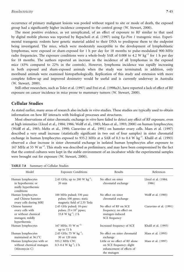
occurrence of primary malignant lesions was pooled without regard to site or mode of death, the exposed
group had a significantly higher incidence compared to the control group (W. Stewart, 2000).
The most positive evidence, as yet unreplicated, of an effect of exposure to RF similar to that used
by digital mobile phones was reported by Repacholi et al. (1997) using Em-Pim 1 transgenic mice. Experi-
mental transgenic rodents have genetic material added to their DNA to predispose them to the endpoint
being investigated. The mice, which were moderately susceptible to the development of lymphoblastic
lymphomas, were exposed or sham-exposed for 1 h per day for 18 months to pulse-modulated 900-MHz
radio frequencies. The exposure conditions were a whole-body SAR of 0.008 to 4.2 W kg–1 for 1 h per day
for 18 months. The authors reported an increase in the incidence of all lymphomas in the exposed
mice (43% compared to 22% in the controls). However, lymphoma incidence was rapidly increasing
in both exposed and sham-exposed animals when the study was terminated; in addition, only
moribund animals were examined histopathologically. Replication of this study and extension with more
complete follow-up and improved dosimetry would be useful and is currently underway in Australia
(W. Stewart, 2000).
Still other researchers, such as Toler et al. (1997) and Frei et al. (1998a,b), have reported a lack of effect of RF
exposure on cancer incidence in mice prone to mammary tumors (W. Stewart, 2000).
Cellular Studies
As stated earlier, many areas of research also include in vitro studies. These studies are typically used to obtain
information on how RF interacts with biological processes and structures.
Most observations of sister chromatic exchange in vitro have failed to detect any effect of RF exposure, even
at high intensities (Lloyd et al., 1984; 1986; Wolff et al., 1985; Maes et al., 1993; 2000) on human lymphocytes;
(Wolff et al., 1985; Meltz et al., 1990; Ciaravino et al., 1991) on hamster ovary cells. Maes et al. (1997)
described a very small increase (statistically significant in two out of four samples) in sister chromatid
exchange in human lymphocytes exposed to 935.2 MHz at a SAR of 0.3 to 0.4 W kg–1. Khalil et al. (1993)
observed a clear increase in sister chromatid exchange in isolated human lymphocytes after exposure to
167 MHz at 55 Wm–2. This study was described as preliminary, and may have been compromised by the fact
that the control cultures were kept in the stable environment of an incubator while the experimental samples
were brought out for exposure (W. Stewart, 2000).
TABLE 7.8 Summary of Cellular Studies
Model Exposure Conditions Results References
Human lymphocytes
in hypothermic or
midly hyperthermic
conditions
2.45 GHz; up to 200 W kg–1;
20 min
No effect on sister
chromatid exchange
Lloyd et al. (1984;
1986)
Human lymphocytes
and Chinese hamster
ovary cells during MRI
100 MHz pulsed; 330 msecpulses; 100 ppsec; static
magnetic field of 2.35 Tesla
No effect on sister
chromatid exchange
Wolff et al. (1985)
Chinese hamster
ovary cells with
or without chemical
mutagen; mildly
hyperthermic
2.45 GHz pulsed; 10-msecpulses; 25 · 103 ppsec;33.8 W kg–1; 2 h
No effect of RF on SCE
frequency; no effect on
mutagen-induced
SCE frequency
Ciaravino et al. (1991)
Human lymphocytes 167 MHz; 55 W m–2;
up to 72 h
Increased frequency of SCE Khalil et al. (1993)
Human lymphocytes
maintained at 36.1–C2.45 GHz; 75 W kg–1;
30 or 120 min
No effect on sister chromatid
exchange
Maes et al. (1993)
Human lymphocytes with or
without chemical mutagen
(Mitomycin C)
935.2 MHz CW;
0.3–0.4 W kg–1; 2 h
Little or no effect of RF alone
on SCE frequency; slight
enhancement of effects of
the mutagen
Maes et al. (1997)
7-45Bioelectricity
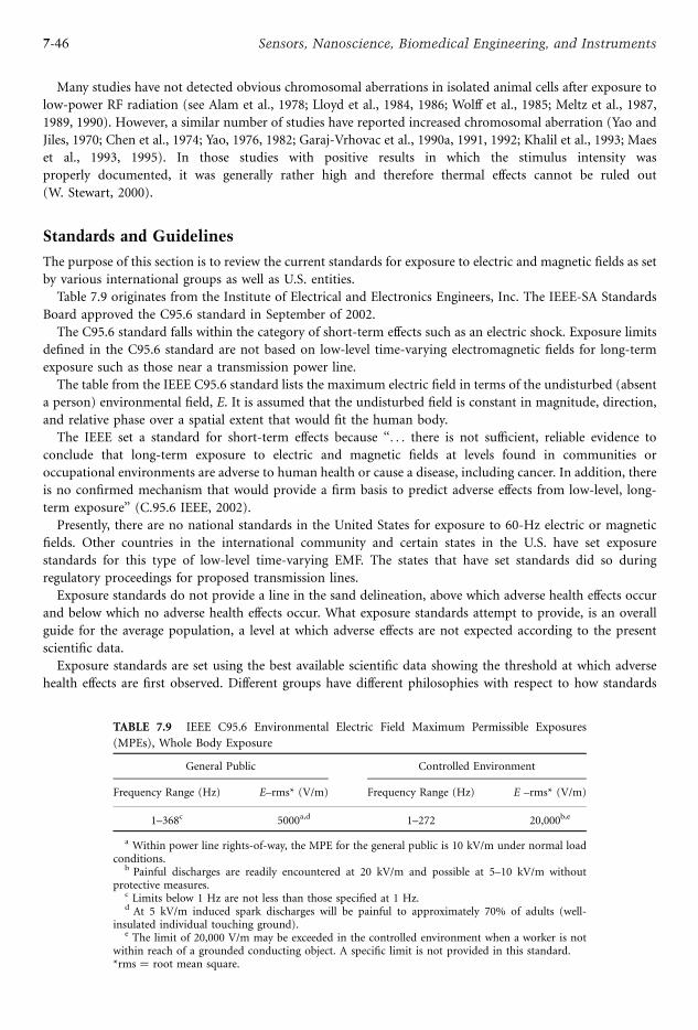
Many studies have not detected obvious chromosomal aberrations in isolated animal cells after exposure to
low-power RF radiation (see Alam et al., 1978; Lloyd et al., 1984, 1986; Wolff et al., 1985; Meltz et al., 1987,
1989, 1990). However, a similar number of studies have reported increased chromosomal aberration (Yao and
Jiles, 1970; Chen et al., 1974; Yao, 1976, 1982; Garaj-Vrhovac et al., 1990a, 1991, 1992; Khalil et al., 1993; Maes
et al., 1993, 1995). In those studies with positive results in which the stimulus intensity was
properly documented, it was generally rather high and therefore thermal effects cannot be ruled out
(W. Stewart, 2000).
Standards and Guidelines
The purpose of this section is to review the current standards for exposure to electric and magnetic fields as set
by various international groups as well as U.S. entities.
Table 7.9 originates from the Institute of Electrical and Electronics Engineers, Inc. The IEEE-SA Standards
Board approved the C95.6 standard in September of 2002.
The C95.6 standard falls within the category of short-term effects such as an electric shock. Exposure limits
defined in the C95.6 standard are not based on low-level time-varying electromagnetic fields for long-term
exposure such as those near a transmission power line.
The table from the IEEE C95.6 standard lists the maximum electric field in terms of the undisturbed (absent
a person) environmental field, E. It is assumed that the undisturbed field is constant in magnitude, direction,
and relative phase over a spatial extent that would fit the human body.
The IEEE set a standard for short-term effects because ‘‘. . . there is not sufficient, reliable evidence to
conclude that long-term exposure to electric and magnetic fields at levels found in communities or
occupational environments are adverse to human health or cause a disease, including cancer. In addition, there
is no confirmed mechanism that would provide a firm basis to predict adverse effects from low-level, long-
term exposure’’ (C.95.6 IEEE, 2002).
Presently, there are no national standards in the United States for exposure to 60-Hz electric or magnetic
fields. Other countries in the international community and certain states in the U.S. have set exposure
standards for this type of low-level time-varying EMF. The states that have set standards did so during
regulatory proceedings for proposed transmission lines.
Exposure standards do not provide a line in the sand delineation, above which adverse health effects occur
and below which no adverse health effects occur. What exposure standards attempt to provide, is an overall
guide for the average population, a level at which adverse effects are not expected according to the present
scientific data.
Exposure standards are set using the best available scientific data showing the threshold at which adverse
health effects are first observed. Different groups have different philosophies with respect to how standards
TABLE 7.9 IEEE C95.6 Environmental Electric Field Maximum Permissible Exposures
(MPEs), Whole Body Exposure
General Public Controlled Environment
Frequency Range (Hz) E–rms* (V/m) Frequency Range (Hz) E –rms* (V/m)
1–368c 5000a,d 1–272 20,000b,e
a Within power line rights-of-way, the MPE for the general public is 10 kV/m under normal loadconditions.
b Painful discharges are readily encountered at 20 kV/m and possible at 5–10 kV/m withoutprotective measures.
c Limits below 1 Hz are not less than those specified at 1 Hz.d At 5 kV/m induced spark discharges will be painful to approximately 70% of adults (well-
insulated individual touching ground).e The limit of 20,000 V/m may be exceeded in the controlled environment when a worker is not
within reach of a grounded conducting object. A specific limit is not provided in this standard.*rms ¼ root mean square.
7-46 Sensors, Nanoscience, Biomedical Engineering, and Instruments
should be set by using differing interpretations of the levels at which biological changes are observed. In the
United States, standards have typically been set by finding the level where clearly demonstrated and
reproducible damage is known to first occur, and then multiplying by a safety factor. Typical safety factors are
in the range of 10 to 50. Figure 7.26 and Figure 7.27 show levels at which effects are observed in electric and
magnetic fields. Some groups include exposure data that indicate that biological changes may occur, but where
clearly reproducible hazards have not been demonstrated. This often leads to significantly lower exposure
limits. The Soviet Union had standards that were approximately 1000 times lower than the U.S. standards for
radio frequency exposures and the enforcement of these standards was also very different. Therefore, it does
not automatically follow that, above a given limit, exposure is harmful.
In 2001, an expert scientific working group of WHO’s International Agency for Research on Cancer (IARC)
reviewed studies related to the carcinogenicity of static and extremely low-frequency (ELF) electric and
magnetic fields. Using the standard IARC classification that weighs human, animal, and laboratory evidence,
FIGURE 7.26 Thresholds of magnetic field effects. (Source: J. Bernhart.)
FIGURE 7.27 Thresholds of electrical field effects. (Source: J. Bernhart.)
7-47Bioelectricity
ELF magnetic fields were classified as possibly carcinogenic to humans based on epidemiological studies of
childhood leukemia (WHO, 2002). An example of a well-known agent classified in the same category is coffee,
which may increase risk of kidney cancer, while at the same time be protective against bowel cancer. ‘‘Possibly
carcinogenic to humans’’ is a classification used to denote an agent for which there is limited evidence of
carcinogenicity in humans and less than sufficient evidence for carcinogenicity in experimental animals. While
the classification of ELF magnetic fields as possible carcinogenic to humans has been made by the IARC, it
remains possible that there are other explanations for the observed association between exposure to ELF
magnetic fields and childhood leukemia (WHO, 2002).
Table 7.10 is exposure standards from the International Commission on Non-Ionizing Radiation Protection
(ICNIRP) and it pertains to European power at 50 Hz.
Many countries in the international community set their own national standards for exposure to
electromagnetic fields. However, the majority of these national standards draw on guidelines set by ICNIRP.
This non-governmental entity, formally recognized by the World Health Organization (WHO), evaluates
scientific results from all over the world. Based on an in-depth review of the literature, ICNIRP produces
guidelines recommending limits on exposure. These guidelines were last updated in April 1998 (WHO, 2002).
Not all standards and guidelines throughout the world have recommended the same limits for exposure to
cell phones and base stations. For example, some published exposure limits in Russia and some eastern
European countries have been generally more restrictive than existing or proposed recommendations for
exposure developed in North America and other parts of Europe (Cleveland, Jr. et al., 1995).
The exposure limits adopted by the Federal Communications Commission (FCC) in 1996, based on the
ANSI/IEEE and NCRP guidelines, are expressed in terms of electric and magnetic field strength and power
density for transmitters operating at frequencies from 300 kHz to 100 GHz are shown in Table 7.11.
The FCC also adopted limits for localized (‘‘partial body’’) absorption in terms of specific absorption rate
(SAR), shown in Table 7.12, that apply to certain portable transmitting devices such as hand-held cellular
telephones (Cleveland et al., 1995).
In 1998 the ICNIRP published its own guidelines covering exposure to RF radiation. These were based on
essentially the same evidence as that used by the National Radiation Protection Board (NRPB), and for
workers the limits of exposure are similar. However, under the ICNIRP guidelines, the maximum levels of
exposure of the public are about five times less than those recommended for workers. The reason for this
approach was the possibility that some members of the general public might be particularly sensitive to RF
radiation. However, no detailed scientific evidence to justify the additional safety factor was provided (Stewart
report).
The ICNIRP guidelines for the public have been incorporated in a European Council Recommendation
(1999), which has been agreed to in principle by all countries in the European Union, including the U.K. In
Germany, the ICNIRP guidelines have been incorporated into a statute (Stewart report).
The ICNIRP guidelines are presented with reference levels and these reflect the factor of five differences
between the public and occupational basic restrictions. The ICNIRP public reference levels for the frequencies
used by mobile phones are shown in Table 7.14. Reference levels for mobile communications in the frequency
range 800 to 1000 MHz are from 4 to 5 W m–2 and for 1800 to 1900 MHz from 9 to 9.5 W m–2 (ICNIRP,
1998a).
TABLE 7.10 Summary of the ICNIRP Exposure Guidelines for European Power
European Power Frequency
Frequency 50 Hz 50 Hz
Electric field (V m–1) Magnetic field (mT)Public exposure limits 5,000 100
Occupational exposure limits 10,000 500
Source: World Health Organization, 2003.
7-48 Sensors, Nanoscience, Biomedical Engineering, and Instruments

TABLE 7.11. FCC Limits for Maximum Permissible Exposure (MPE)
Frequency Range (MHz)
Electric Field
Strength (H)
(V/m)
Magnetic Field
Strength (H)
(A/m)
Power Density
(S) (mW/cm2)
Averaging Time
jHj2·jHj2or S (min)
(A) Limits for Occupational/Controlled Exposure
0.3 3.0 614 1.63 (100)* 6
3.0–30 1842/f 4.89/f (900/f 2)* 6
30–300 61.4 0.163 1 6
300–1500 F/300 6
1500–100,000 5 6
(B) Limits for General Population/Uncontrolled
0.3–1.34 614 1.63 (100)* 30
1.34–30 824/f 2.19/f (180/f 2)* 30
30–300 27.5 0.073 0.2 30
300–1500 f/1500 30
1500–100.000 1 30
f ¼ frequency in MHz
Source: OET Bulletin 56, 4th ed., 08/1999, FCC.*Plane-wave equivalent power density.
TABLE 7.12 FCC Limits for Localized (Partial-Body) Exposure
Specific Absorption Rate (SAR)
Occupational/Controlled Exposure
(100 kHz to 6 GHz)
General Uncontrolled/Exposure
(100 kHz to 6 GHz)
,0.4 W kg–1 whole-body ,0.08 W kg–1 whole-body
<0.08 W kg–1 partial-body <1.6 W kg–1 partial-body
Source: OET Bulletin 56, 4th ed., 08/1999, FCC.
TABLE 7.13. ICNIRP Basic Restrictions on Occupational Exposure and General Public
Exposure (in parentheses) in the Frequency Range 10 MHz to 10 GHz
Tissue Region SAR Limit (W kg–1) Mass (g) Time (min)
Whole body 0.4 (0.08) — 6
Head, trunk 10 (2) 10 6
Limbs 20 (4) 10 6
Source: ICNIRP, 1998.
TABLE 7.14 ICNIRP Reference Levels for Public Exposure at Mobile
Telecommunications Frequencies
Electric Field Magnetic Field Power Density
Frequency (MHz) Strength (V/M) Strength (A m–1) (W m–2)
400–2000 1.375f1/2 0.0037f1/2 f/200
2000–3000 61 0.16 10
f is the frequency in MHz.Source: ICNIRP, 1998.
7-49Bioelectricity

Risk
There is growingmovement throughout the world to adopt precautionary approaches formanagement of health
risks in the face of scientific uncertainty and the assessment of potential health risks from EMF includes
numerous uncertainties. ‘‘The Precautionary Principle is a risk management policy applied in circumstances
with a high degree of scientific uncertainty, reflecting the need to take action for a potentially serious risk without
awaiting the results of scientific research.’’1
On February 2, 2000, the European Commission approved guidelines for the application of the
Precautionary Principle and these guidelines should be:
. Tailored to the chosen level of protection
. Nondiscriminatory in their application, i.e., they should treat comparable situations in a similar way
. Consistent with similar measures already taken, i.e., they should be comparable in scope and nature to
measures already taken in equivalent areas in which all scientific data are available. Based on an examination of the potential benefits and costs of action or lack of action (including,
where appropriate and feasible, an economic cost/benefit analysis). Provisional in nature, i.e. subject to review in the light of new scientific data. Capable of assigning responsibility for producing the scientific evidence necessary for a more
comprehensive risk assessment1
‘‘People are disturbed, not by things, but by their view of them.’’
—Epictetus
In trying to understand people’s perception of risk, it is important to distinguish between a health hazard
and a health risk. A hazard can be an object or a set of circumstances that could potentially harm a person’s
health. Risk is the likelihood, or probability, that a person will be harmed by a particular hazard. Driving a car
is a potential health hazard. Driving a car fast presents a risk. The higher the speed, the more risk is associated
with the driving (WHO, 2002).
The nature of the risk can lead to different perceptions. The more factors that are added to the public’s
perception of risk, the greater the potential for concern. The following pairs of characteristics of a situation
generally affect risk perception:
. Familiar vs. Unfamiliar Technology
Familiarity with a given technology or a situation helps reduce the level of the perceived risk. The
perceived risk increases when the technology or situation, such as EMF, is new, unfamiliar, or hard-to-
comprehend (WHO, 2002).
. Personal Control vs. Lack of Control over a Situation
If people do not have any say about installation of power lines and mobile telephone base stations,
especially near their homes, schools, or play areas, they tend to perceive the risk from such EMF
facilities as being high (WHO, 2002).
. Voluntary vs. Involuntary Exposure
People feel much less at risk when the choice is theirs. Those who do not use mobile telephones may
perceive the risk as high from the low RF fields emitted from mobile telephone base stations. However,
mobile telephone users generally perceived the risk as low from the much more intense RF fields of their
voluntarily chosen handsets (WHO, 2002).
. Dreaded vs. Not Dreaded Outcome
Some diseases and health conditions, such as cancer, or severe and lingering pain, are more feared than
others. Thus, even a small possibility of cancer, especially in children, from a potential hazard such as
EMF exposure receives significant public attention (WHO, 2002).
1Electromagnetic Fields and Public Health Cautionary Policies, 2000.
7-50 Sensors, Nanoscience, Biomedical Engineering, and Instruments

. Direct vs. Indirect Benefits
If people are exposed to electric and magnetic fields from a high-voltage transmission line that does not
provide power to their community, they may not perceive any direct benefit from the installation and
are less likely to accept the associated risk (WHO, 2002).
. Fair vs. Unfair Exposure
Issues of social justice may be raised because of unfair EMF exposure. If facilities were installed in poor
neighborhoods for economic reasons (e.g., cheaper land), the local community would perceive the
potential risks as being an unfair burden (WHO, 2002).
The risk of developing cancer or being in an automobile accident is described in several ways, the most
common being lifetime risk and relative risk. Lifetime risk is the probability that an individual will develop
cancer or be involved in an auto accident sometime between birth and death. For example, the lifetime risk of
breast cancer in American women is now one in eight (i.e., one woman in eight can expect to develop breast
cancer sometime in her life). This may seem like a frightening number but it is also misleading because the
risks are really very different for different age groups, particularly for pre- and postmenopausal women. The
lifetime risk for death from an automobile accident is 1 in 70.
The risk of developing a cancer is usually described in terms of relative risk. Relative risk is calculated by
dividing the incidence rate of disease in a group exposed to a suspected carcinogen or risk factor by the
incidence of disease in a non-exposed group. The relative risk for average smokers developing lung cancer is
9.9. This means that smokers are about ten times more likely to develop lung cancer relative to nonsmokers
(Risk and Cancer, 2003). A relative risk of 1.0 indicates a risk no greater than that of the comparison group
used in a study. A relative risk of less than 1.0 indicates lower risk, or a protective effect. Many relative risks are
in the range of 1.3 or 1.5, meaning that the exposed person has a 30% or 50% greater chance of developing the
disease than an unexposed person (Risk and Cancer, 2003). The following table shows some relative risk
factors for various cancers.
Monson (1980) characterized the significance of relative risk levels as follows:
It has been suggested by epidemiologists that cause-and-effect associations are only clearly established when
relative risks are large (i.e., five or more) and when data from epidemiological studies are consistent.
Risk of developing cancer from exposure to a carcinogen is also evaluated by excess lifetime cancer risk. The
EPA uses this terminology in regulating some chemicals, and remediating Superfund sites. The EPA uses a
Relative Risk Strength of Association
1.0–1.2 None
1.2–1.5 Weak
1.5–3.0 Moderate
3.0–10.0 Strong
Above 10.0 Infinite
TABLE 7.15 Relative Risk Factors for Disease Factors
Factor (Cancer Type) Relative Risk References
Smoking (lung cancer) 10–40 Wynder and Hoffman (1982)
Benzene, occupational exposure (leukemia) 1.5–20 Sandler and Collman (1987)
Asbestos, occupational exposure (lung cancer) 2–6 Fraumeni and Blot (1982)
Prenatal x-ray exams (childhood cancer) 2.4 Harvey et al. (1985)
Hair dye (leukemia) 1.8 Cantor et al. (1988)
Powerlines (childhood cancer) 1.5–3 Wertheimer and Leeper (1979), Savitz et al. (1988)
Saccharin (bladder cancer) 1.5–2.6 IARC (1987)
Excessive alcohol (oral cancer) 1.4–2.3 Tuyns (1982)
Coffee (bladder cancer) 1.3–2.6 Morrison and Cole (1982)
Source: J. Lee, Bonneville Power Administration.
7-51Bioelectricity

target level of one in a million (10–6) excess lifetime cancer risk from long-term exposure. This is the
probability that at a specific exposure level in a population, one extra person out of a million will develop
cancer in their lifetime. This is considered a de minimus risk because it is many times below other risks which
people face every day, and pales in comparison to the about one in four chance that an American has of
developing cancer in their lifetime.
Reducing the perceived risk involves countering the factors associated with personal risk. Members of
communities feel they have a right to know what is proposed and planned with respect to the construction
of EMF sources that, in their opinion, might affect their health. They need to have some control and be
part of the decision-making process. New EMF technologies will be mistrusted and feared unless an effective
system of public information and communication among stakeholders is established.
Conclusion
The purpose of this section was to provide the electrical professional with information on the biological
effects of electric and magnetic fields. Effects from electric shock are the best understood and a cause-and-
effect relationship is known. Burns from electric shock are different from other kinds of burns and the
destruction is most venerable to muscle and nerve tissue. The biological effects of EMF from power lines,
cell phones, and base stations are more problematic as a cause–effect relationship has not been proven.
These issues are also very controversial and the data on health effects from power lines, cell phones, and
base stations continues to be inconclusive. Guidelines and standards differ vastly due to differing
philosophies with respect to the incomplete understanding of the thresholds and mechanisms of the
biological effect of EMFs. Finally, the controversy surrounding health effects from power lines, cell phones,
and base stations is due to the perception of risk and the more factors that are added to the public’s
perception of risk, the greater the potential for concern.
Reference
L.E. Anderson and L.B. Sasser, ‘‘Electromagnetic fields and cancer: laboratory studies,’’ Electromagnetic Fields
Biological Interactions and Mechanisms: Advances in Chemistry Series 250, Washington, DC: American
Chemical Society, pp. 225–234, 1995.
Bernhart, J., personal communication.
Jefferson Lab, ‘‘Biological Effects of Electric Shock,’’ 2003, Jefferson Lab EH&S, 2004,,http://www.jlab.org/ehs/
manual/EHSbook-404.html..
M. Blank and R. Goodman, ‘‘Electromagnetic fields may act directly on DNA,’’ J. Cell Biochem., 75, 369–374,
Dec. 1999.
M. Blank, and L. Soo, ‘‘Enhancement of cytochrome oxidase activity in 60 Hz magnetic fields,’’ Bioelectrochem.
Bioenerg., 253–259, 1998.
J.L. Buthod, W. Engdahl, J.R. Gauger, and W.R. Adey, ‘‘Influence of 60 Hz magnetic fields and 12-0-tet
radecanoylphorbol-13-acetate on expression of c-myc in HL-60 cells, Abstract P-209A,’’ presented at the
18th Annual Meeting of the Bioelectromagnetics Society, Victoria, BC, Canada, 1996, p. 179.
‘‘C95.6, IEEE standard for safety levels with respect to human exposure to electromagnetic fields, 0–3 kHz,’’
IEEE Stand. Coordinating Comm., 28, 2002 (approved September 12).
Cleveland, Jr., Robert F., and Jerry L. Ulcek. ‘‘Questions and answers about biological effects and potential
hazards of radiofrequency electromagnetic fields,’’ OET Bulletin 56. Fed. Commun. Comm., 1999,
pp. 1–36.
R. Cleveland, D.M. Sylvar, J.L. Ulcck, and E.D. Mantiply, ‘‘Measurement of radiofrequency fields and potential
exposure from land-mobile paging and cellular radio base station antennae. Abstracts,’’ 17th Annual
Meeting of the Bioelectromagnetics Society, Boston, MA, 1995, p. 188.
Draft National Research Council Report on PAVE PAWS Radar, 1/13/05.
7-52 Sensors, Nanoscience, Biomedical Engineering, and Instruments

‘‘Electric Shock Precautions,’’ 2004, ,http://pchem.scs.uiuc.edu/pchemlab/eletric.htm.
‘‘Electromagnetic Fields and Public Health Cautionary Policies,’’ March 2000, WHO Backgrounder,
World Health Organization, ,http://www.who.int/docstore/peh-emf/publications/facts_press/EMF-
Precaution.htm., 2004.
‘‘Electromagnetic Fields and Public Health, Mobile Telephone and Their Base Stations, Fact Sheet N193,’’ June
2000, http://www.who.int/docstore/peh-emf/publications/facts-press/efact/World Health Organization,
2004
EMF RAPID, ‘‘EMF electric and magnetic fields associated with the use of electric power: questions and
answers,’’ prepared by the National Institute of Environmental Health Sciences, National Institutes of
Health, sponsored by the NIEHS/DOE EMF RAPID Program, 1995.
WHO, ‘‘Establishing a dialogue on risks from electromagnetic fields,’’ Radiation and Environmental Health,
Geneva, Switzerland: Department of Protection of the Human Environment, World Health
Organization, 2002.
M. Feychting and A. Ahlbom, ‘‘Childhood leukemia and residential exposure to weak extremely low frequency
magnetic fields,’’ Environ. Health Perspect., Suppl. 2, 59–62, March 1995.
J.P. Fulton, S. Cobb, L. Preble, L. Leone, and E. Forman, ‘‘Electrical wiring configuration and childhood
leukemia in Rhode Island,’’ Am. J. Epidemiol., 111, 292–296, March 1980.
R. Goodman, H. Lin, M. Jin, and M. Blank, ‘‘The cellular stress response is induced by electromagnetic fields.
Abstract A-4-1,’’ presented at the 18th Annual Meeting of the Bioelectromagnetics Society, Victoria, BC,
Canada, p. 13.
S.W. Hui, G.P. Jahreis, Y.L. Zhao, and P.G. Johnson, ‘‘Effect of 60 Hz magnetic field on proto-oncogene
transcription. Abstract P-213A,’’ Presented at the 18th Annual Meeting of the Bioelectromagnetics
Society, Victoria, BC, Canada, 1996.
ICNIRP, ‘‘Guidelines for limiting exposure to time-varying electric, magnetic and electromagnetic fields (up to
300 GHz),’’ Health Phys., vol. 74, no. 4, pp. 494–522, April 1998.
T.L. Jones, ‘‘Magnetic fields and cancer (correspondence),’’ Environ. Health Perspect., vol. 101, no. 5, pp.
368–369, 1993.
T.L. Jones, C.H. Shih, D.H. Thurston, B.J. Ware, and P. Cole, ‘‘Selection bias from differential residential
mobility as an explanation for associations of wire codes with childhood cancer,’’ J. Clin. Epidemiol., 46,
546–548, 1993.
T.L. Jones, C.H. Shih, D.H. Thurston, B.J. Ware, and P. Cole, ‘‘Response to: bias in studies of electromagnetic
fields (letter to the editor),’’ J. Clin. Epidemiol, vol. 47, p. 1083, 1994.
B. Junkersdorf, H. Bauer, and H.O. Gutzeit, ‘‘Electromagnetic fields enhance the stress response at elevated
temperatures in the nematode Caenorhabditis elegans,’’ Bioelectromagnetics, vol. 21, pp. 100–106, 2000.
J. Lee, K. Semple Pierce, C. Spiering, R.D. Stearns, and G. VanGinhoven, Electrical and Biological Effects of
Transmission Lines: A Review, Portland, Oregon: Bonneville Power Administration, December 1996.
R.C. Lee, ‘‘Physical mechanisms of tissue injury in electrical trauma,’’ IEEE Trans. Educ., vol. 34, pp. 223–
230, 1991.
H. Lin, M. Opler, M. Head, M. Blank, and R. Goodman, ‘‘Electromagnetic field exposure induces rapid
transitory heat shock factor activation in human cells,’’ J. Cell Biochem., 66, 482–488, 1997.
M. Linet, E. Hatch, R. Kleinerman, L. Robison, W. Kaune, D. Friedman, R. Severson, C. Haines, C. Hartsock,
S. Niwa, S. Wacholder, and R. Tarone, ‘‘Residential exposure to magnetic fields and acute lymphoblastic
leukemia in children,’’ New Engl. J. Med., July, 1–7, 1997.
W. Loscher and M. Mevissen, ‘‘Animal studies on the role of 50/60-Hertz magnetic fields in carcinogenesis,’’
Life Sci., vol. 54, pp. 1531–1543, 1994.
M.O. Mattson, K.H. Mild, and U. Valtersson, ‘‘Are there transcriptional effects in Jurkat cells exposed to a
50-Hz magnetic field? Abstract P-81A,’’ 18th Annual Meeting of the Bioelectromagnetics Society,
Victoria, BC, Canada, 1996, p. 127.
M. Mevissen, M. Haussler, M. Szamel, A. Emmendorffer, S. Thun-Battersby, and W. Loscher, ‘‘Complex effects
of long-term 50 Hz magnetic field exposure in vivo on immune functions in female Sprague-Dawley
rats depend on duration of exposure,’’ Bioelectromagnetics, vol. 19, pp. 259–270, 1998.
7-53Bioelectricity

M. Mevissen, W. Loscher, and M. Szamel, ‘‘Exposure of DMBA-treated Female Rats in a 50-Hz 50 mTmagneticfield: effects on mammary tumor growth, melatonin levels, and T lymphocyte activation,’’
Carcinogenesis, vol. 17, no. 5, pp. 903–910, 1994.
T. Miyakawa, S. Yamada, S. Harada, T. Ishimori, H. Yamanoto, and R. Hosono, ‘‘Exposure of caenorhabditis
elegans to extremely low frequency high magnetic fields induces stress responses,’’ Bioelectromagnetics,
vol. 22, pp. 333–339, 2001.
R.R. Monson, Occupational Epidemiology, 2nd ed., Boca Raton, FL: CRC Press, 1990, p. 94.
K.K. Murthy, W.R. Rogers, and H.D. Smith, ‘‘Initial studies on the effects of combined 60 Hz electric and
magnetic field exposure on the immune system of nonhuman primates,’’ Bioelectromagnetics, Suppl. 3,
93–102, 1995.
National Research Council, ‘‘An Assessment of Potential Health Effects from Exposure to PAVE Paws Low-
Level Phased-Array Radiofrequency Energy,’’ National Research Council Report, January 2005.
C.R. Nave and B.C. Nave, Physics for the Health Sciences, 3rd ed., Philadelphia, PA: W.B. Saunders, 1985.
D. Olden, ‘‘NIEHS report on health effects from exposure to power-line frequency electric and magnetic
fields,’’ National Institute of Environmental Health Sciences, National Institutes of Health, NIH
Publication No. 99-4493.
ORAU Panel on Health Effects of Low-Frequency Electric and Magnetic Fields, ‘‘EMF and cancer (letter),’’
Science, 260, 13–16, 1993.
R.D. Owen, L.W. Cress, A.B. Desta, H.E. Sprehn, and D.P. Thomas, ‘‘ELF–EMF replication studies: gene
expression and enzyme activity. Abstract P-229A,’’ Presented at the 18th Annual Meeting of the
Bioelectromagnetics Society, Victoria, BC, Canada, 1996, p. 189.
Bass Associates Inc., ‘‘The Physical Effects of Electricity,’’ Electrocution Thresholds for Humans, February
2004, ,http://www.bassengineering.com/E_Effect.htm..
‘‘Risk and Cancer,’’ November 2003, ,http://www.acs.ohio-state.edu/units/cancer/handbook/risk.pdf..
L.E. Rogers, N.R. Warren, K.A. Hinds, R. E. Gano, R.E. Fitzner, and G.F. Piepel, ‘‘Environmental studies of a
1100-kV prototype transmission line: an annual report for the 1981 study period,’’ Prepared by Battelle
Pacific Northwest Laboratories for Bonneville Power Administration, 1982.
D.A. Savitz, H. Wachtel, F.A. Barnes, E.M. John, and J.G. Tvrdik. ‘‘Case-control study of childhood cancer and
exposure to 60-Hz magnetic fields,’’ Am. J. Epidemiol., 128, 21–38, 1988.
D.A. Savitz and W.T. Kaune, ‘‘Childhood cancer in relation to a modified residential wire code,’’ Environ.
Health Perspect., 101, 76–80, 1993.
D.A. Savitz and D.P. Loomis, ‘‘Magnetic field exposure in relation to leukemia and brain cancer mortality
among electric utility workers,’’ Am. J. Epidemiol., 141, 123–134, 1995.
B. Shi, R.R. Isseroff, and R. Nuccitelli, ‘‘Twenty and 60 Hz 80 gauss electromagnetic fields do not enhance the
rate of protein synthesis in human skin fibroblasts. Abstract P-227A,’’ presented at the 18th Annual
Meeting of the Bioelectromagnetics Society, 1996, p. 187.
W. Stewart, ‘‘Mobile Phones and Health,’’ 11 May 2000, Independent Expert Group on Mobile Phones, 2004,
,http://www.iegmp.org.uk/report/text.htm..
R. Thompon, Siting and Land Rights, Minneapolis, MN: Xcel Energy Inc., 2003.
S.J. Thurston and J.D. Saffer, ‘‘Cellular effects of weak electromagnetic fields. Abstract P-215A,’’ Presented at
the 18th Annual Meeting of the Bioelectromagnetics Society, Victoria, BC, Canada, 1996, p. 182.
N. Wertheimer and E. Leeper, ‘‘Electrical wiring configuration and childhood cancer,’’ Am. J. Epidemiol., 109,
273–284, 1979.
N. Wertheimer and E. Leeper, ‘‘Re: electrical wiring configurations and childhood leukemia in Rhode Island,’’
Am. J. Epidemiol., 16, 461–462, 1980.
N. Wertheimer, D.A. Savitz, and E. Leeper, ‘‘Childhood cancer in relation to indicators of magnetic fields from
ground current sources,’’ Bioelectromagnetics, 16, 86–69, 1995.
World Health Organization, ‘‘What are Electromagnetic Fields?’’ 2003, http://www.who.int/peh-emf/about/
WhatisEMF/en/print.html
CTIA, ‘‘WOW–COM World of Wireless Communications–CTIA,’’ Cellular Telecommunications & Internet
Associationm, January 2005, ,www.wow-com.com..
7-54 Sensors, Nanoscience, Biomedical Engineering, and Instruments
7.4 Embedded Signal Processing
David R. Martinez, Robert A. Bond, and M. Michael Vai
Introduction
The term embedded signal processing refers to the digital signal processing functionality that is part of a larger
system. Embedded signal processing has been used in a broad range of applications, including consumer
electronics, automotive, telecommunications, medical, and military. Among all these application domains,
however, military systems continue to be one of the dominant users of high-performance embedded
computing (HPEC). Although the technologies in military applications are drawn from commercial enablers,
their usage is adapted to very demanding embedded systems.
The capabilities demanded by military systems differ from other industries in very distinct ways. One
important difference is the often paramount requirement for small size, weight, and power (SWAP). Another
important difference, which is shared by industrial and automotive control applications but is not always
critical in other areas, is the need for hard real-time performance; this requirement emerges because the system
must meet stringent system deadlines and cannot tolerate any failures in the middle of a military combat
situation. A third distinction is a demand for low latencies to convert sensor data to information, to
knowledge, and finally to understanding useful to the user. These capabilities are feasible only if the hardware
can support them. In addition to demanding hardware capabilities, the software needed in these systems also
becomes increasingly complex.
Throughout this section, the military sensor application of embedded signal processing is frequently drawn
upon as a challenging example to illustrate the demands in computing, memory, and interconnects, as well as
the requisite development techniques and standards. Therefore, let us begin by defining a representative
military embedded signal processing system. Such a system will be part of a payload typically consisting of
front-end sensing and other hardware (e.g., RF array, EO camera, receivers, sensor timing and control, etc.).
The signal processing system starts at the output of the analog-to-digital converters (ADCs) and ends, for
onboard computations in an unmanned vehicle or satellite application, at the input to a communication
antenna connected to a wireless network.
In particular, our discussion focuses on a generic military embedded signal processing architecture
representative of active electronically steered array (AESA)-based sensor systems, such as ground moving
target indicator (GMTI) radar or synthetic aperture radar (SAR) (see section ‘‘Generic Embedded Signal
Processing Architecture’’). In the last ten years, there has been significant emphasis on advancing AESA sensor
systems. Improvements in ADCs make it feasible and affordable to bring digital sampling closer to the antenna
array, which simplifies the front-end analog electronics. Furthermore, recent advances in computing
technologies make it affordable to exploit the flexibility of AESA antenna using very high performance
embedded computers for signal and image processing.
These AESA systems will consist of hundreds to thousands of sensor channels, with data rates exceeding tens
to hundreds of billion bytes per second (driven by the ADC sampling rates). The demands in computation will
exceed tens of trillion of operations per second (TOPS). Even though there are special purpose processors with
the ability to perform TOPS in computation, the large data rates demand that the computation be distributed
across many parallel processors working on different portions of the incoming data. The challenge is to
efficiently balance the input and output (I/O) with the holding memory (buffers to hold incoming data and
intermediate data products) and the real-time computation. This balance must be accomplished with SWAP
restricted to a size of a fraction of a cubic meter (or equivalently a few cubic feet1), power in the tens to
hundreds of watts, and weight not exceeding tens of kilograms. These constraints can be seen to be quite severe
when one considers that, for more challenging applications, the power efficiency needed approaches 100,000
million operations per second per watt (MOPS/W) and the required computing density is nearly 100,000
1This section uses a mix of metric and English units. All numbers expressed in ft3 can be converted to m3 by applying a 0.03
factor.
7-55Bioelectricity
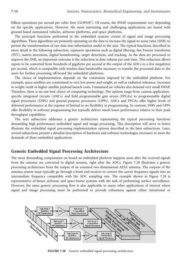
billion operations per second per cubic foot (GOPS/ft3). Of course, the SWAP requirements vary depending
on the specific applications. However, the most interesting and challenging applications are found with
ground-based unmanned vehicles, airborne platforms, and space platforms.
The principal functions performed in the embedded systems consist of signal and image processing
algorithms. These algorithms are primarily operating on the data to increase the signal-to-noise ratio (SNR) to
permit the transformation of raw data into information useful to the user. The typical functions, described in
more detail in the following subsection, represent operations such as digital filtering, fast Fourier transforms
(FFT), matrix inversions, digital beamforming, target detections, and tracking. As the data are processed to
improve the SNR, an important outcome is the reduction in data volume per unit time. This reduction allows
inputs to be converted from hundreds of gigabytes per second at the output of the ADCs to a few megabytes
per second, which is compatible with wireless data bandwidths necessary to transfer the processed data to the
users for further processing off-board the embedded platforms.
The choice of implementation depends on the constraints imposed by the embedded platform. For
example, space satellites are constrained to very low power and weight, as well as radiation tolerance. Increases
in weight result in higher satellite payload launch costs. Unmanned air vehicles also demand very small SWAP.
Therefore, there is no one best choice of computing technology. The options range from custom application-
specific integrated circuits (ASICs) and field programmable gate arrays (FPGAs) to programmable digital
signal processors (DSPs) and general-purpose processors (GPPs). ASICs and FPGAs offer higher levels of
delivered performance at the expense of limited to no flexibility in programming. In contrast, DSPs and GPPs
offer flexibility in software programming but typically deliver much lower performance relative to their peak
throughput capabilities.
The next subsection addresses a generic architecture representing the typical processing functions
demanding high performance embedded signal and image processing. This description will serve to better
illustrate the embedded signal processing implementation options described in the later subsections. Later,
several subsections present a detailed description of hardware and software technologies necessary to meet the
demands of these embedded applications.
Generic Embedded Signal Processing Architecture
The most demanding computation on board an embedded platform happens soon after the received signals
from the antenna are converted to digital streams, right after the ADCs. Figure 7.28 illustrates a generic
processing architecture from the output of an assumed two-dimensional AESA antenna. The outputs of the
antenna system must typically go through a front-end receiver to convert the carrier frequency signals into an
intermediate frequency compatible with the ADC sampling rate. The example shown in Figure 7.28 is
representative of future airborne and space-borne systems with the task of performing surface surveillance.
However, the same generic processing flow is also applicable to many other applications of interest where
signal and image processing must be performed to provide robustness against either intentional or
FIGURE 7.28 Generic embedded signal processing architecture.
7-56 Sensors, Nanoscience, Biomedical Engineering, and Instruments
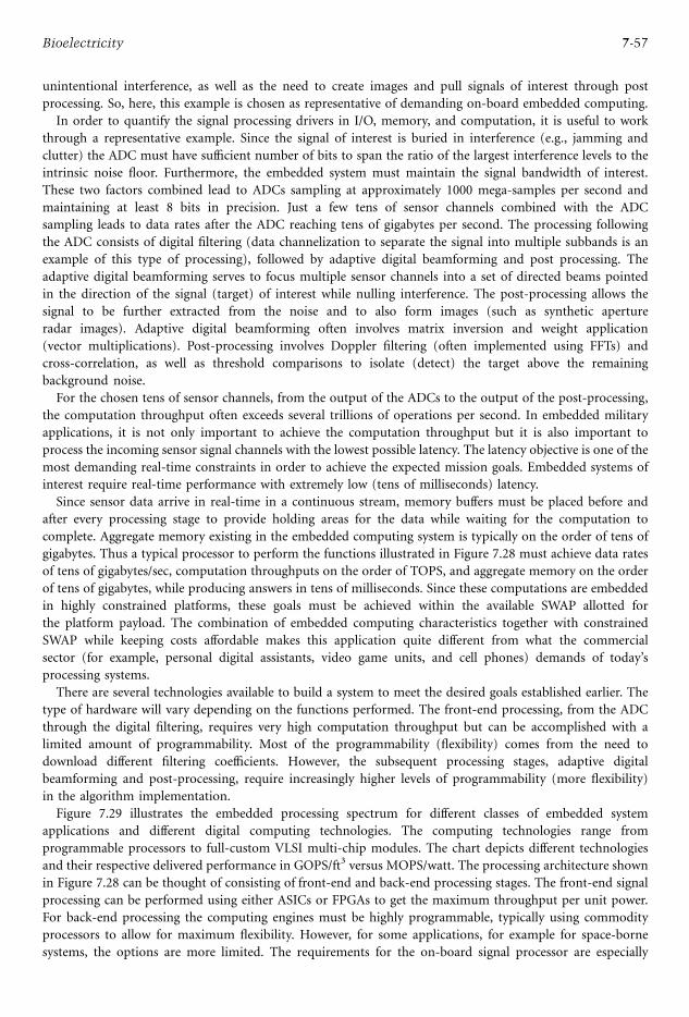
unintentional interference, as well as the need to create images and pull signals of interest through post
processing. So, here, this example is chosen as representative of demanding on-board embedded computing.
In order to quantify the signal processing drivers in I/O, memory, and computation, it is useful to work
through a representative example. Since the signal of interest is buried in interference (e.g., jamming and
clutter) the ADC must have sufficient number of bits to span the ratio of the largest interference levels to the
intrinsic noise floor. Furthermore, the embedded system must maintain the signal bandwidth of interest.
These two factors combined lead to ADCs sampling at approximately 1000 mega-samples per second and
maintaining at least 8 bits in precision. Just a few tens of sensor channels combined with the ADC
sampling leads to data rates after the ADC reaching tens of gigabytes per second. The processing following
the ADC consists of digital filtering (data channelization to separate the signal into multiple subbands is an
example of this type of processing), followed by adaptive digital beamforming and post processing. The
adaptive digital beamforming serves to focus multiple sensor channels into a set of directed beams pointed
in the direction of the signal (target) of interest while nulling interference. The post-processing allows the
signal to be further extracted from the noise and to also form images (such as synthetic aperture
radar images). Adaptive digital beamforming often involves matrix inversion and weight application
(vector multiplications). Post-processing involves Doppler filtering (often implemented using FFTs) and
cross-correlation, as well as threshold comparisons to isolate (detect) the target above the remaining
background noise.
For the chosen tens of sensor channels, from the output of the ADCs to the output of the post-processing,
the computation throughput often exceeds several trillions of operations per second. In embedded military
applications, it is not only important to achieve the computation throughput but it is also important to
process the incoming sensor signal channels with the lowest possible latency. The latency objective is one of the
most demanding real-time constraints in order to achieve the expected mission goals. Embedded systems of
interest require real-time performance with extremely low (tens of milliseconds) latency.
Since sensor data arrive in real-time in a continuous stream, memory buffers must be placed before and
after every processing stage to provide holding areas for the data while waiting for the computation to
complete. Aggregate memory existing in the embedded computing system is typically on the order of tens of
gigabytes. Thus a typical processor to perform the functions illustrated in Figure 7.28 must achieve data rates
of tens of gigabytes/sec, computation throughputs on the order of TOPS, and aggregate memory on the order
of tens of gigabytes, while producing answers in tens of milliseconds. Since these computations are embedded
in highly constrained platforms, these goals must be achieved within the available SWAP allotted for
the platform payload. The combination of embedded computing characteristics together with constrained
SWAP while keeping costs affordable makes this application quite different from what the commercial
sector (for example, personal digital assistants, video game units, and cell phones) demands of today’s
processing systems.
There are several technologies available to build a system to meet the desired goals established earlier. The
type of hardware will vary depending on the functions performed. The front-end processing, from the ADC
through the digital filtering, requires very high computation throughput but can be accomplished with a
limited amount of programmability. Most of the programmability (flexibility) comes from the need to
download different filtering coefficients. However, the subsequent processing stages, adaptive digital
beamforming and post-processing, require increasingly higher levels of programmability (more flexibility)
in the algorithm implementation.
Figure 7.29 illustrates the embedded processing spectrum for different classes of embedded system
applications and different digital computing technologies. The computing technologies range from
programmable processors to full-custom VLSI multi-chip modules. The chart depicts different technologies
and their respective delivered performance in GOPS/ft3 versus MOPS/watt. The processing architecture shown
in Figure 7.28 can be thought of consisting of front-end and back-end processing stages. The front-end signal
processing can be performed using either ASICs or FPGAs to get the maximum throughput per unit power.
For back-end processing the computing engines must be highly programmable, typically using commodity
processors to allow for maximum flexibility. However, for some applications, for example for space-borne
systems, the options are more limited. The requirements for the on-board signal processor are especially
7-57Bioelectricity
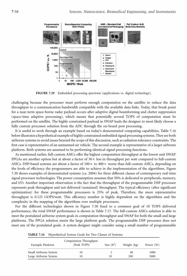
challenging because the processor must perform enough computation on the satellite to reduce the data
throughput to a communication bandwidth compatible with the available data links. Today, that break point
for a near-term space-borne radar payload occurs after adaptive digital beamforming and clutter suppression
(space-time adaptive processing), which means that potentially several TOPS of computation must be
performed on the satellite. The highly constrained payload in SWAP leads the designer to most likely choose a
fully custom processor solution from the ADC through the on-board post processing.
It is useful to work through an example based on today’s demonstrated computing capabilities. Table 7.16
below illustrates a hypothetical example of highly constrained embedded signal processing systems. They are both
airborne systems to avoid issues beyond the scope of this discussion, such as radiation tolerance constraints. The
first case is representative of an unmanned air vehicle. The second example is representative of a larger airborne
platform. Both systems are assumed to be performing identical signal processing functions.
As mentioned earlier, full-custom ASICs offer the highest computation throughput at the lowest unit SWAP.
FPGAs are another option but at about a factor of 30 · less in throughput per watt compared to full-custom
ASICs. DSP-based systems are about a factor of 100 · to 400 · worse than full-custom ASICs, depending on
the levels of efficiency the programmers are able to achieve in the implementation of the algorithms. Figure
7.30 shows examples of demonstrated systems (ca. 2004) for three different classes of contemporary real-time
signal processor technologies. The power consumption assumes that 50% is dedicated to peripherals, memory,
and I/O. Another important observation is the fact that the throughput of the programmable DSP processor
represents peak throughput and not delivered (sustained) throughput. The typical efficiency (after significant
optimization) for these programmable processors is 25% of peak. Therefore, the more representative
throughput is 0.125 GOPS/watt. This efficiency number is highly dependent on the algorithms and the
complexity in the mapping of the algorithms over multiple processors.
For the different technologies shown in Figure 7.30 fixed to a common goal of 10 TOPS delivered
performance, the total SWAP performance is shown in Table 7.17. The full-custom ASICs solution is able to
meet the postulated airborne system goals in computation throughput and SWAP for both the small and large
platforms. The FPGA solution meets the large platform goals. The programmable DSP processor does not
meet any of the postulated goals. A system designer might consider using a small number of programmable
FIGURE 7.29 Embedded processing spectrum (applications vs. digital technology).
TABLE 7.16 Hypothetical System Goals for Two Classes of Systems
Example Platform
Computation Throughput
(Peak TOPS) Size (ft3) Weight (kg) Power (W)
Small Airborne System 10 2 40 1000
Large Airborne System 10 10 200 5000
7-58 Sensors, Nanoscience, Biomedical Engineering, and Instruments
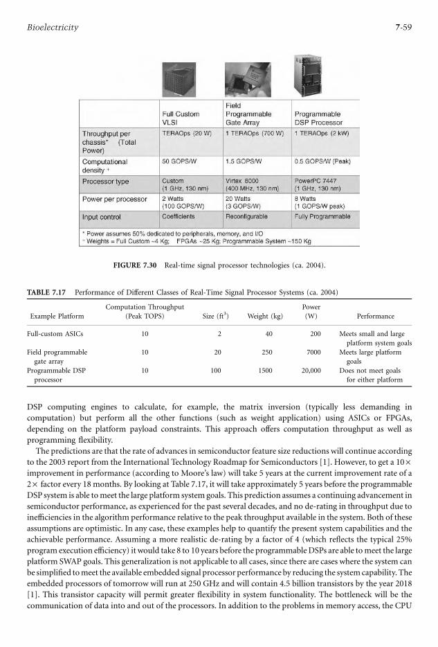
DSP computing engines to calculate, for example, the matrix inversion (typically less demanding in
computation) but perform all the other functions (such as weight application) using ASICs or FPGAs,
depending on the platform payload constraints. This approach offers computation throughput as well as
programming flexibility.
The predictions are that the rate of advances in semiconductor feature size reductions will continue according
to the 2003 report from the International Technology Roadmap for Semiconductors [1]. However, to get a 10·improvement in performance (according to Moore’s law) will take 5 years at the current improvement rate of a
2· factor every 18 months. By looking at Table 7.17, it will take approximately 5 years before the programmable
DSP system is able tomeet the large platform system goals. This prediction assumes a continuing advancement in
semiconductor performance, as experienced for the past several decades, and no de-rating in throughput due to
inefficiencies in the algorithm performance relative to the peak throughput available in the system. Both of these
assumptions are optimistic. In any case, these examples help to quantify the present system capabilities and the
achievable performance. Assuming a more realistic de-rating by a factor of 4 (which reflects the typical 25%
program execution efficiency) it would take 8 to 10 years before the programmableDSPs are able tomeet the large
platform SWAP goals. This generalization is not applicable to all cases, since there are cases where the system can
be simplified tomeet the available embedded signal processor performance by reducing the systemcapability. The
embedded processors of tomorrow will run at 250 GHz and will contain 4.5 billion transistors by the year 2018
[1]. This transistor capacity will permit greater flexibility in system functionality. The bottleneck will be the
communication of data into and out of the processors. In addition to the problems in memory access, the CPU
FIGURE 7.30 Real-time signal processor technologies (ca. 2004).
TABLE 7.17 Performance of Different Classes of Real-Time Signal Processor Systems (ca. 2004)
Example Platform
Computation Throughput
(Peak TOPS) Size (ft3) Weight (kg)
Power
(W) Performance
Full-custom ASICs 10 2 40 200 Meets small and large
platform system goals
Field programmable
gate array
10 20 250 7000 Meets large platform
goals
Programmable DSP
processor
10 100 1500 20,000 Does not meet goals
for either platform
7-59Bioelectricity
will be unacceptably high in power consumption; and no end in sight is foreseen. The computing farmwill likely
be distributed across the platform and not localized at a single physical location, thereby permitting optimumuse
of the constrained space available.
The software complexity will significantly dominate the overall cost of the system. Today, one can purchase
embedded system hardware for about $1/MFLOP (system based on PowerPCG4 CPUs and a significant amount
ofmemory at each node). Therefore, a trillion operations per second embedded system can be procured for about
$1M.However, the application softwarewill consist of 200K to 1M software source lines of code (SLOC). Analysis
of software development often equates 10 SLOCs to the cost of a single PC station; that is, 10 SLOCs cost about
$500. Therefore, the cost of software development, for lines debugged and tested, can range from $10M to $40M
(for 200K to 1M SLOCs, respectively)! It is important to clarify that these estimates are for a full software suite,
including sensor timing, command, and control. For just signal processing, the software cost may be somewhat
lower because of the more stream-like data flow dependency present in the algorithms.
The above costs only include the acquisition of the embedded system to the point where one is ready to
integrate it with the remaining payload. Additional costs must be accounted for during the integration and
testing of the embedded computing system with the sensor and overall payload package. These costs are
directly dependent on the functionality expected of the platform system. Experience indicates that these costs
can be a significant percentage of the total system cost. However, the integration and testing can be simplified
if each respective part of the overall payload package is carefully tested independently, but verified end-to-end
against a set of established ‘‘golden’’ test vectors and algorithms. These independent systems should also
comply with open standards to allow easier hardware and software refresh as technology matures, and to allow
for the reuse of hardware and software components. The following sections elaborate on implementation
approaches and best practices to effectively develop high performance embedded signal processor systems.
Embedded Digital Signal Processor (DSP)
This subsection discusses the use of programmable processors in embedded digital signal processing. Today,
programmable technologies find wide use in virtually every embedded signal and image processing domain. In
the consumer electronics and telecommunications markets programmable implementations account for about
40% of the DSP market [2], and their market share is expected to grow. Programmable devices are employed
in speech, video, multimedia applications, wired and wireless telecommunications, voice-over-IP and
streaming video Internet, as well as short-range communications such as Bluetooth, EDCT, and DECT.1 High-
end consumer electronics such as HDTV and set-top boxes employ programmable DSPs. Programmable DSPs
are used in multimedia applications that require support for multiple video compression techniques such as
MPEG-2, MPEG-4, and H.264. The automotive industry now relies on programmable embedded computing
for sensor processing and engine control. The medical industry employs programmable signal processing in
sophisticated sensing and imaging applications such as MRI and ultrasound.
DSPs and GPPs have become widespread in modern military sensor signal processing applications such as
sonar, radar, ladar, and passive optical sensors (cameras as well as optical and infrared CCD arrays). With the
advent of the software radio, programmable processors are also becoming prevalent in military
communications. They are found in virtually all military platforms of all sizes; submarines, ships, manned
aircraft, UAVs (unmanned aerial vehicles), satellites, missiles, and torpedoes. They are used at practically all
scales. A modern torpedo may use on the order of a dozen DSPs to perform its front-end active sonar signal
processing. Modern radars and sonars often require programmable throughput in the range of 10 to 1000
billion FLOPS (GFLOPS) and employ tens to thousands of DSPs and GPPs.
Advantages of Programmable DSP
Programmable signal processing solutions have the principal advantages of increased flexibility and faster
time-to-market. Changes in functionality can be rapidly accomplished through software changes.
1DECT is the Digital European Cordless Telephone reference design and EDCT is the U.S. Enhanced Digital Cordless Telephone
reference design.
7-60 Sensors, Nanoscience, Biomedical Engineering, and Instruments

Design specification changes can be incorporated later in the development cycle and new applications can be
implemented faster in software than with custom hardware designs. Thus, software implementations allow
new capabilities to be specified later and to enter the marketplace sooner and thereby provide a competitive
advantage. Moreover, software can more readily accommodate additional features, leading to product
differentiation that can make the difference between success and failure in the highly competitive consumer
marketplace. Finally, product fixes and upgrades can be made in the field, which allows for a cost-effective way
to evolve product lines and serves to reduce development risks.
In the military domain, programmable solutions allow the military electronics industry to exploit advances in
commercial-off-the-shelf (COTS) processor technologies. With moderate ruggedization, low-cost COTS
processor chips, boards, and systems can be employed inmany military sensor applications. This capability leads
to reduced development and production costs and faster development time. It also avoids expensive, custom
processor technology developments. However, the military use of COTS processors brings the need to deal with
COTS technology refresh and obsolescence, as discussed later in section ‘‘Challenges of Programmable DSP’’.
Development and production costs figure prominently in the designer’s choice between fixed function and
programmable DSP approaches. Because of lower development costs programmable approaches are generally
preferred for low production volumes, provided that SWAP constraints can be met. However, there are
exceptions; for example, if the longest possible battery life is desired, low-power ASICs might be the best
solution regardless of production volumes.
When larger production runs are involved, as in the case of consumer electronics products, the tradeoff can
be complex. Both fixed-function and programmable technologies enjoy the Moore’s law performance
advancement trends of semiconductor process technology. However, the entry cost of chip fabrication has
grown exponentially as feature sizes have continued to shrink. For example, as lithography sizes approach
90 nm, mask costs for ASICs are exceeding $1M per mask [2]. Thus, the unit production volume necessary to
justify ASICs continues to grow exponentially as feature sizes shrink. However, popular commercial DSPs and
GPPs are produced in large quantities (and used across multiple applications), so the up-front design and
fabrication set-up costs are amortized across much larger unit volumes.
Challenges of Programmable DSP
Form-factor issues such as SWAP are the principal challenges facing programmable DSP implementations. In a
custom, fixed-function hardware solution, the hardware performs the precise functionality required by the
application. For a defined functional capability and a chosen technology, a fixed-function hardware design can
be optimized to meet SWAP constraints. The designer is free to exploit the details of the computations to
minimize resource utilization. However, programmable processors by their very nature are not as form-factor
efficient as fixed-function hardware. Whether DSPs, GPPs, or media processors, the circuitry is less than 100%
efficient on any specific algorithm, since the design is aimed at attaining generally high average efficiency over a
larger set of applications. The key to effective use of programmable processors, therefore, is the efficient use of
the hardware resources by the software program. Inefficient software implementations require more hardware
resources to meet a given throughput and latency requirement. More hardware implies higher power
consumption, heat generation, and cost, as well as larger size and greater weight. In form-factor constrained
consumer applications, such as a handheld or mobile devices, inefficient software translates directly into
reduced capability; either less functionality in the software, or shorter battery life, or larger size. In a military
application, reduced capability may not be an option; demanding form-factor constraints consequently drive
the design toward custom hardware solutions. This is especially the case in the front-end of a sensor system,
where the signal processing tends to be better suited to custom hardware due to the simpler, more regular
computations and the need for extremely high throughput.
Programmable processor technology improvements occur at a rapid pace. Within a specific processor
family, new processors appear in the marketplace at 18-month to 2-year intervals. Once newer versions are
available, production of the older versions is curtailed. Thus, applications and products using these earlier
processors face the issue of hardware obsolescence. In military systems, the problem is exacerbated by the
extremely long platform life cycles. It can take several years to design and develop a radar or sonar and once
deployed these systems can remain in use for decades. Thus, several generations of COTS processor upgrades
7-61Bioelectricity
span the lifetime of these military systems. A strategy of lifetime buys of spare parts is occasionally employed,
but at some point the growing requirements of the system outstrip the performance capabilities of the obsolete
hardware, at which time a major hardware upgrade and a software re-implementation are needed. A better
strategy is to build processor-independent software implementations at the outset that can be readily ported to
new processors as they emerge in the marketplace. This permits a more regular, less disruptive COTS hardware
refresh cycle. This approach is also attractive in the commercial domain. The ability to reuse intellectual
property (IP) captured in software implementations allows developers to exploit new processor technologies
for higher performance, which in turns allows new capabilities to be added to a product line. Being able to
port the IP software to the new processor, rather than having to re-develop it, leads to faster time to market
and reduced development costs. Thus, the key lifecycle challenge in embedded signal processing is to build
portable, reusable software that is also highly efficient.
For large signal processing applications such as military radars or medical ultrasound products, the scale of
the system is another key challenge. These systems often involve over 100,000 lines of highly optimized signal
processing code. Not only must the software be designed for performance and portability, but it must also be
designed to run on parallel processors consisting of tens or even thousands of processing units. Middleware,
discussed below, is a key enabler of portability and scalability in high-end embedded signal processing systems.
Programmable DSP Hardware
Programmable DSPs emerged as a distinct class of processor in the late 1970s. They have evolved through
several generations [3] and today range widely in both cost and performance. In general, programmable DSPs
are designed to provide high throughput, low latency, power efficient programmable implementations of
signal processing applications. To do this, they must address the key computational characteristics of typical
signal processing algorithms. Signal processing computations are characterized by:
1. Continuous or long streams of digitized data samples that are acted on by signal processing functions.
After a processing delay, the processed results are output continuously and concurrently with the input
stream. This implies that a processor must have processing and I/O capabilities that are matched to the
input data rates, the algorithm complexity, and the output data rates. Also, I/O and processing need to
occur concurrently and continuously.
2. Multiplication, addition, and accumulation (summation) operations. Most basic signal processing
functions, such as FIR, IIR, FFT, convolution, inner products, and others, are based on simple loops
involving multiplies, adds, and accumulation of results. The FFT requires a butterfly operation, which
consists of a special sequence of multiplies, sign changes, and additions.
3. Relatively simple and regular computation flow-of-control. Signal and image processing algorithms tend
to proceed through a straightforward series of mathematical transformations. Looping is required to
support vector and matrix mathematics, but complex program flows with irregular or global data
memory accesses are rare.
4. Intrinsic data parallelism. Often, the same operation needs to be applied to different data, and
dependencies from one sample, vector, or matrix to the next are weak. Thus, there are opportunities to
apply operations in parallel across data sets.
5. Multidimensional datasets. For more complex applications, the data streams are often multidimensional.
For example, in the AESA radar example discussed earlier, the data representing the returns from a
transmitted waveform are digitized and input into the signal processor from each receiver channel (or, in
some cases, from each analog beam of a sub-array). The waveform for each channel is divided into
multiple pulse repetition intervals. Thus, each sample is multidimensional, representing the return for a
particular pulse, channel, and range gate.
To handle signal processing efficiently, digital signal processors have the following features [3,4]:
1. High-speed data interfaces to handle input and output data streams. The interfaces are designed to
minimize the need for main processor intervention and control. Typically, they have their own direct
memory access (DMA) circuitry and interact with the main processor through low-overhead interrupts
7-62 Sensors, Nanoscience, Biomedical Engineering, and Instruments
and memory mapped control registers. Some DSPs, such as the SHARC ADSP21060, are designed to
work in multi-processor configurations and have direct processor-to-processor communication ports.
2. Specially designed architectures referred to as Harvard1 architectures. In Harvard architectures, separate
buses are provided for data and instruction memory accesses. Usually, distinct data and instruction
address spaces are provided, along with dedicated address generation hardware that can execute in
parallel with the main processor unit. In a more conventional GPP architecture, the operands and the
operation (program instruction) are accessed sequentially over a single bus, resulting in the need for
multiple clock cycles per instruction. The main goal of the Harvard architecture is to remove this
memory bottleneck. Data and instructions can be accessed concurrently, thereby permitting single-cycle
instruction execution. Furthermore, through special auto-increment and address stride instructions,
separate address generation hardware allows the next data to be accessed immediately after the current
data are processed; the main unit does not need to pause to compute the new data locations.
3. Highly optimized, dedicated hardware for multiply-accumulate (MAC) operations. Additionally, some
processors, such as the Analog Devices SHARC DSP, have specialized instructions and hardware for
butterfly operations to support FFTs. Many DSPs also have parallel execution units, for example, dual
MAC units as found in the Analog Devices TigerSHARC DSP.
4. On-chip instruction and data memories to allow complete datasets and programs to be ‘‘close’’ to the
processing units. While general purpose microprocessors provide both data and instruction caches, the
logic that controls cache contents is hardwired and designed for good average performance on general
codes. DSPs provide programmable control over on-chip memories, so that programs can explicitly
control the placement of highly optimized, repetitive inner loop codes, and the data that these code
operate on, in the high speed, zero wait state on-chip memory.
5. Special data address increment and stride instructions as well as dedicated loop control hardware, to
efficiently handle the short inner loops found in many signal processing kernels. Since DSP algorithms
such as FIR, convolution, inner product, up and down sampling, etc., often involve short,
computationally intensive inner loops, the loop control overhead must be kept to a minimum. In
conventional processors, it often takes several instructions to implement a conditional loop or to
calculate addresses for data striding. DSPs have dedicated hardware optimized to minimize this overhead.
Major DSP vendors include Lucent, Texas Instruments, Motorola, NEC, and Analog Devices. These vendors
produce DSPs with most or all of the features described above. Sophisticated fourth-generation, high-end
DSPs have recently entered the marketplace that provide additional enhancements and improved performance.
For example, the VelociTI TMS320C62xx from Texas Instruments provides support for very-long-instruction-
word (VLIW) processing. VLIW architectures achieve high performance through the parallel issuance and
execution of multiple instructions [4]. Today, all major DSP vendors employ multiple-issue architectures for
their highest performing DSPs. Although VLIW-based processors allow for very high performance, this benefit
tends to come at the expense of lower code density (programs require more instruction memory) and higher
power consumption.
DSP products either support just fixed-point or both fixed-point and floating-point arithmetic. Fixed-point
processors provide the advantage that they can be very power efficient. However, fixed-point DSPs are more
difficult to program than their floating-point counterparts. A typical fixed-point DSP has several different
precision fixed-point representations: 8, 16, 32, and often 24 bits. The programmer must explicitly mix and
match operations between these different precisions, and must handle arithmetic underflow, overflow, and
finite-precision effects. In floating-point, there are typically single and double precision representations. Most
applications can be implemented completely in single precision floating point, and checks for underflow and
overflow are not required. A few modern applications, such as certain radar adaptive processing
implementations, have such large dynamic ranges that double precision arithmetic is required. Nevertheless,
underflow and overflow are generally not issues in floating-point arithmetic, whereas they are very relevant in
fixed-point representations and require special programming considerations.
1Named for the work done at Harvard University in the 1940s under Howard Aiken.
7-63Bioelectricity
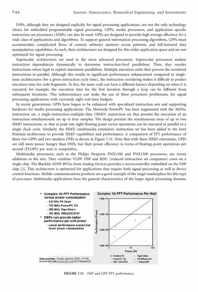
DSPs, although they are designed explicitly for signal processing applications, are not the only technology
choice for embedded programmable signal processing. GPPs, media processors, and application specific
instruction-set processors (ASIPs) can also be used. GPPs are designed to provide high average efficiency for a
wide class of applications and algorithms. To support general information processing algorithms, GPPs must
accommodate complicated flows of control, arbitrary memory access patterns, and full-featured data
manipulation capabilities. As such, their architectures are designed for this wider application space and are not
optimized for signal processing.
Superscalar architectures are used in the more advanced processors. Superscalar processors analyze
instruction dependencies dynamically to determine instruction-level parallelism. Then, they reorder
instructions where legal to exploit maximum parallelism. Multiple execution units then process the reordered
instructions in parallel. Although this results in significant performance enhancement compared to single-
issue architectures (for a given instruction cycle time), the instruction reordering makes it difficult to predict
execution time for code fragments. In fact, the same code can have a different latency depending on when it is
executed; for example, the execution time for the first iteration through a loop can be different from
subsequent iterations. This indeterminacy can make the use of these processors problematic for signal
processing applications with extremely tight real-time budgets.
In recent generations, GPPs have begun to be enhanced with specialized instruction sets and supporting
hardware for media processing applications. The Motorola PowerPC has been augmented with the AltiVec
instruction set, a single-instruction-multiple-data (SIMD) instruction set that permits the execution of an
instruction simultaneously on up to four samples. The design permits the simultaneous issue of up to two
SIMD instructions, so that at peak rate eight floating point vector operations can be executed in parallel in a
single clock cycle. Similarly, the MMX (multimedia extension) instruction set has been added to the Intel
Pentium architecture to provide SIMD capabilities and performance. A comparison of FFT performance of
these two GPPs and two modern DSPs is shown in Figure 7.31. Note that with these SIMD extensions, GPPs
are still more power hungry than DSPs, but their power efficiency in terms of floating-point operations per
second (FLOPS) per watt is competitive.
Multimedia processors, such as the Philips Nexperia PNX1300 and PNX1500 processors, are recent
additions to the mix. They combine VLIW DSP and RISC (reduced instruction set computers) cores on a
single chip. The Blackfin ADSP-BF5xx from Analog Devices provides a microcontroller embedded on the DSP
chip [2]. This architecture is optimized for applications that require both signal processing as well as device
control functions. Mobile communications products are a good example of the target marketplace for this type
of processor. Multimedia applications have the general characteristics of the larger signal processing domain,
FIGURE 7.31 DSP and GPP FFT performance.
7-64 Sensors, Nanoscience, Biomedical Engineering, and Instruments
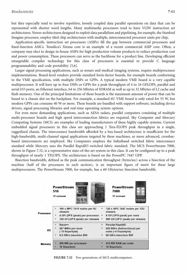
but they especially tend to involve repetitive, loosely coupled data parallel operations on data that can be
represented with shorter word lengths. Many multimedia processors tend to have VLIW instruction set
architectures. Newer architectures designed to exploit data parallelism and pipelining, for example, the Stanford
Imagine processor, employ tiled chip architectures with multiple, interconnected processor units per chip,
Application-specific instruction set processors (ASIPs) fill the gap between commercial processors and
fixed-function ASICs. Tensilica’s Xtensa core is an example of a recent commercial ASIP core. Often, a
company may elect to design in-house ASIPs for high production volume products to reduce production cost
and power consumption. These processors can serve as the backbone for a product line. Developing efficient
retargetable compiler technology for this class of processors is essential to provide C language
programmability and code portability [5,6].
Larger signal processing applications, such as sonars and medical imaging systems, require multiprocessor
implementations. Board-level vendors provide standard form-factor boards, for example boards conforming
to the VME specification, with multiple DSPs or GPPs. A typical modern VME board is a very capable
multiprocessor. It will have up to four DSPs or GPPs for a peak throughput of 4 to 16 GFLOPS, parallel and
serial I/O ports, an Ethernet interface, 64 to 256 Mbytes of SDRAM as well as up to 32 Mbytes of L2 cache and
flash memory. One of the principal limitations of these boards is the maximum amount of power that can be
bused to a chassis slot on the backplane. For example, a standard 6U VME board is only rated for 55 W, but
modern GPPs can consume 40 Wor more. These boards are bundled with support software, including device
drivers, signal processing libraries and real-time operating system options.
For even more demanding applications, such as AESA radars, parallel computers consisting of multiple
multi-processor boards and high speed interconnection fabrics are required. Sky Computer and Mercury
Computing Systems (MCS) are examples of leading manufacturers of these highly capable systems. Current
embedded signal processors in this class are approaching 1 Tera-FLOPS peak throughput in a single,
ruggedized chassis. The interconnect bandwidth afforded by a bus-based architecture is insufficient for the
high-bandwidth, multi-channel signal applications targeted by these machines, so more advanced, crossbar-
based interconnects are employed. Sky Computers employs the Infiniband switched fabric interconnect
standard while Mercury uses the Parallel RapidIO switched fabric standard. The MCS PowerStream 7000,
shown in Figure 7.32, is a representative state-of-the-art system in this class. It can be configured up to a peak
throughput of nearly 1 TFLOPS. The architecture is based on the PowerPC 7447 GPP.
Bisection bandwidth, defined as the peak communication throughput (bytes/sec) across a bisection of the
machine (half of the processors in each section), is an important figure of merit for these large
multiprocessors. The PowerStream 7000, for example, has a 60 Gbytes/sec bisection bandwidth.
FIGURE 7.32 Two generations of MCS multicomputers.
7-65Bioelectricity
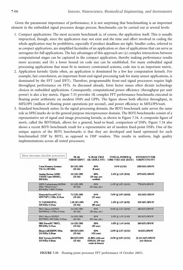
Given the paramount importance of performance, it is not surprising that benchmarking is an important
element in the embedded signal processor design process. Benchmarks can be carried out at several levels:
1. Compact applications: The most accurate benchmark is, of course, the application itself. This is usually
impractical, though, since the application may not exist and the time and effort involved in coding the
whole application may be prohibitive, especially if product deadlines are tight. Smaller codes, referred to
as compact applications, are simplified facsimiles of an application or class of applications that can serve as
surrogates for full applications. The key advantages of this approach are (a) complex interactions between
computational stages can be captured in the compact application, thereby making performance results
more accurate; and (b) a lower bound on code size can be established. For many embedded signal
processing applications that must fit in memory constrained systems, code size is an important metric.
2. Application kernels: Quite often, an application is dominated by a few key computation kernels. For
example, fast convolution, an important front-end signal processing task for many sensor applications, is
dominated by the FFT (and IFFT). Therefore, programmable front-end signal processors require high
throughput performance on FFTs. As discussed already, form factor issues often dictate technology
choices in embedded applications. Consequently, computational power efficiency (throughput per unit
power) is also a key metric. Figure 7.33 provides 1K complex FFT performance benchmarks executed in
floating point arithmetic on modern DSPs and GPPs. The figure shows both effective throughput, in
MFLOPS (million of floating point operations per second), and power efficiency in MFLOPS/watt.
3. Standard benchmark suites: In the signal processing domain, the BDTi benchmark suite serves the same
role as SPECmarks do in the general purpose microprocessor domain. The BDTi benchmarks consist of a
representative set of signal and image processing kernels, as shown in Figure 7.34. A composite figure of
merit, called the BDTiMark, allows for a general, head-to-head, comparison of DSPs. Figure 7.34 also
shows a recent BDTi benchmark result for a representative set of modern fixed-point DSPs. One of the
unique aspects of the BDTi benchmarks is that they are developed and hand optimized for each
benchmarked DSP by BDTi, as opposed to DSP vendors. This results in uniform, high quality
implementations across all tested processors.
FIGURE 7.33 Floating-point processor FFT performance (8 October 2003).
7-66 Sensors, Nanoscience, Biomedical Engineering, and Instruments

Software: Run-time and Development Environment
DSPs are programmed almost exclusively in either C/Cþþ or assembly language. Assembly programming is
still common practice in many commercial DSP applications for the simple reason that many such
applications require maximum achievable performance. Hand-coded assembly programs that exploit
processor-specific instruction sets are still capable of out-performing signal processing codes generated by the
best C compilers. Typically, assembly codes will be 1.5 to 3 times faster than compiled C code, but can reach as
much as 100 times faster [6]. Assembly code can also be made much more compact, which is an important
goal in embedded applications with limited on-chip or secondary memory. On the negative side, assembly
coding is labor intensive, requires programming expertise not readily available in the computer science
mainstream, and tightly binds the implementation to the host DSP. Thus, performance is purchased at the cost
of increased development time and lack of code portability. Upgrading an assembly-based application to a new
processor requires a significant rewrite of the code. Also, since assembly coding is not a common expertise, it is
often difficult to staff the development team.
The key benefits of C/Cþþ programming are greater programmer productivity, higher quality programs
(fewer defects), the ability to develop very large applications, and code portability. C and Cþþimplementations dominate the large, high-end applications such as radars, sonars, and medical imaging
systems. For these applications, which often exceed 100,000 SLOC, only higher level languages can handle the
size and complexity of the programming task.
One approach to achieving the high performance of assembly code and the productivity of C/Cþþprogramming is to embed (or ‘‘inline’’) into the C/Cþþ code assembly routines that provide highly
optimized implementations of key DSP functions. Usually, the DSP manufacturer will provide a
comprehensive library of such function calls. Often, the assembly routines are wrapped in C calls for
programming convenience. Of course, the introduction of processor-specific assembly routines, whether
wrapped in C code or not, reduces the portability of the implementation.
Ultimately, efficient compiler technology is the key challenge in the adoption of C/Cþþ for embedded
signal processing. Compilers for embedded signal processors need to produce code that is both fast and
compact. This is particularly difficult for DSP architectures, due to their shorter lifetimes relative to GPP
architectures (such as the Pentium and PowerPC) and the numerous DSP architectural specializations.
Efficient C compilers for DSP architectures is an active area of research, with recent work focused on the
creation of retargetable compilers, that is, compilers capable of generating object and executable code for
several different types of DSP [6]. Retargetable compilers rely on abstract representational languages to
FIGURE 7.34 BDTi benchmarks for fixed-point DSPs.
7-67Bioelectricity
describe the target processor architectures. Using these representations, the compilers develop lower
level optimizations tuned to specific processor architectures. These compilers enhance code portability and
can be upgraded along with the evolving processor technology, thereby permitting very high
performance compiler functionality to be developed and optimized incrementally over several processor
generations.
Signal processing applications can also benefit from embedded, real-time operating systems (RTOS). Several
operating system vendors, for example, Wind River, which offers VxWorks and VSPWorks, specialize in
providing highly optimized RTOSs for DSPs and GPPs. The defining characteristic of a real-time OS is that it
delivers deterministic or time-bounded performance. RTOSs need to provide a good balance between
deterministic response, high speed, small footprint (code size), and useful feature sets. The capabilities offered
by RTOSs include:
1. Multitasking and task scheduling: For smaller applications, the processor is dedicated to a single program
and multitasking is not required. However, for applications that are multimodal or multipurpose, such as
multifunction radar or multimedia applications, multitasking is often the preferred technical approach.
This allows the designer to dedicate a separate task to each major system input and mode of operation.
Background and periodic tasks can be interspersed with asynchronous, interrupt-driven tasks. The net
result is a cleaner, more maintainable software architecture. In a real-time system, the important
considerations are support for pre-emptive, priority-based scheduling, support for real-time scheduling
approaches such as earliest-deadline-first (EDA), and fast, bounded, task context switch latency.
2. Interrupt services: Signals typically arrive from external sources over an input port that indicates data
availability through an interrupt. Fast, deterministic interrupts servicing is an important characteristic of
a real-time OS. The ability to disable other interrupt and tasks while an interrupt is being serviced is
essential.
3. Timing services: In order to measure and optimize code performance, and to schedule periodic tasks,
operating system time services are important.
4. Intertask communication, signaling, and synchronization: A signal processing application that requires
multiple tasks will more than likely need to synchronize and communicate between tasks. A front end
data conditioning task may operate at a faster rate than a down-stream task. The ability to communicate
the data from one task to the next and signal the downstream task is needed. For example, in a radar
application, the up-stream task of matched filtering and detection communicates target detection data to
a downstream task that performs tracking. Although middleware libraries such as MPI are often used to
perform data communications, especially for multiprocessor implementations, MPI relies on underlying
OS support.
5. Device drivers: Embedded signal processors receive signals for processing from a variety of different
devices and interfaces. Often, the device is custom-made for the application. An RTOS must provide a
means for installing device drivers and accommodating custom device drivers.
Often, for small devices, the RTOS is left out altogether and the program executes ‘‘on the bare metal.’’
There is, however, a general trend toward reliance on RTOSs as systems grow in complexity, memory becomes
increasingly less expensive, and time-to-market becomes a primary driver. A principal advantage of an RTOS
is that it can provide robust, commonly used, well-tested system-level functionality, thereby reducing the
amount of code that needs to be developed and providing a degree of isolation between the application and
underlying processor. In this way, an RTOS that is widely used provides a degree of portability across
processor types.
Middleware is another important technology for providing code portability. Middleware is software that
delivers high-performance functionality while isolating machine specific details into a lower level software
layer. It provides a standard application programming interface (API) to the user application, so that the
application can be ported with minimal changes to any processor platform that support the middleware.
Computer vendors and third-party vendors can concentrate on providing implementations for several
platforms, allowing an application programmer to program at a higher level of abstraction and in a machine-
independent manner.
7-68 Sensors, Nanoscience, Biomedical Engineering, and Instruments
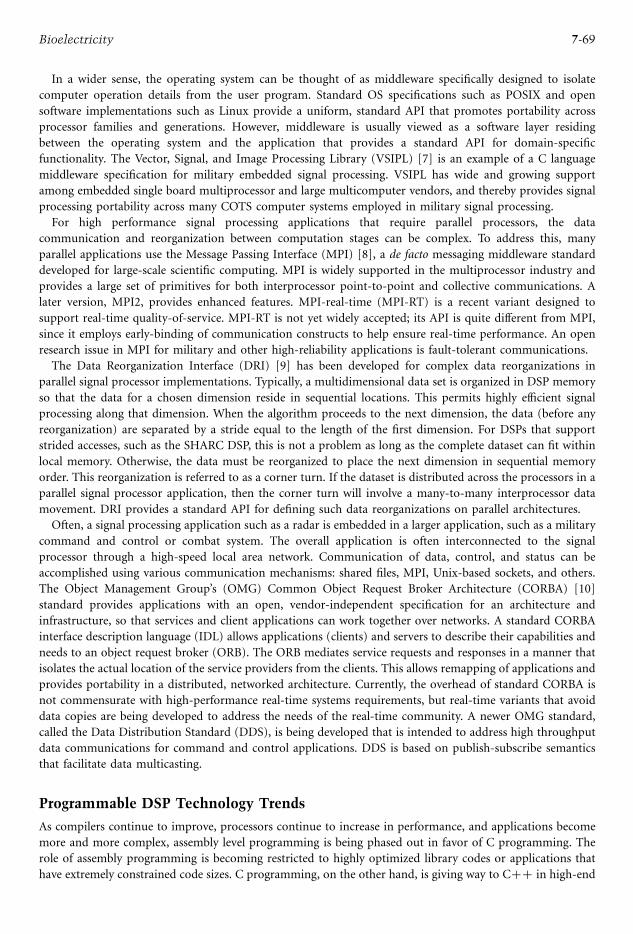
In a wider sense, the operating system can be thought of as middleware specifically designed to isolate
computer operation details from the user program. Standard OS specifications such as POSIX and open
software implementations such as Linux provide a uniform, standard API that promotes portability across
processor families and generations. However, middleware is usually viewed as a software layer residing
between the operating system and the application that provides a standard API for domain-specific
functionality. The Vector, Signal, and Image Processing Library (VSIPL) [7] is an example of a C language
middleware specification for military embedded signal processing. VSIPL has wide and growing support
among embedded single board multiprocessor and large multicomputer vendors, and thereby provides signal
processing portability across many COTS computer systems employed in military signal processing.
For high performance signal processing applications that require parallel processors, the data
communication and reorganization between computation stages can be complex. To address this, many
parallel applications use the Message Passing Interface (MPI) [8], a de facto messaging middleware standard
developed for large-scale scientific computing. MPI is widely supported in the multiprocessor industry and
provides a large set of primitives for both interprocessor point-to-point and collective communications. A
later version, MPI2, provides enhanced features. MPI-real-time (MPI-RT) is a recent variant designed to
support real-time quality-of-service. MPI-RT is not yet widely accepted; its API is quite different from MPI,
since it employs early-binding of communication constructs to help ensure real-time performance. An open
research issue in MPI for military and other high-reliability applications is fault-tolerant communications.
The Data Reorganization Interface (DRI) [9] has been developed for complex data reorganizations in
parallel signal processor implementations. Typically, a multidimensional data set is organized in DSP memory
so that the data for a chosen dimension reside in sequential locations. This permits highly efficient signal
processing along that dimension. When the algorithm proceeds to the next dimension, the data (before any
reorganization) are separated by a stride equal to the length of the first dimension. For DSPs that support
strided accesses, such as the SHARC DSP, this is not a problem as long as the complete dataset can fit within
local memory. Otherwise, the data must be reorganized to place the next dimension in sequential memory
order. This reorganization is referred to as a corner turn. If the dataset is distributed across the processors in a
parallel signal processor application, then the corner turn will involve a many-to-many interprocessor data
movement. DRI provides a standard API for defining such data reorganizations on parallel architectures.
Often, a signal processing application such as a radar is embedded in a larger application, such as a military
command and control or combat system. The overall application is often interconnected to the signal
processor through a high-speed local area network. Communication of data, control, and status can be
accomplished using various communication mechanisms: shared files, MPI, Unix-based sockets, and others.
The Object Management Group’s (OMG) Common Object Request Broker Architecture (CORBA) [10]
standard provides applications with an open, vendor-independent specification for an architecture and
infrastructure, so that services and client applications can work together over networks. A standard CORBA
interface description language (IDL) allows applications (clients) and servers to describe their capabilities and
needs to an object request broker (ORB). The ORB mediates service requests and responses in a manner that
isolates the actual location of the service providers from the clients. This allows remapping of applications and
provides portability in a distributed, networked architecture. Currently, the overhead of standard CORBA is
not commensurate with high-performance real-time systems requirements, but real-time variants that avoid
data copies are being developed to address the needs of the real-time community. A newer OMG standard,
called the Data Distribution Standard (DDS), is being developed that is intended to address high throughput
data communications for command and control applications. DDS is based on publish-subscribe semantics
that facilitate data multicasting.
Programmable DSP Technology Trends
As compilers continue to improve, processors continue to increase in performance, and applications become
more and more complex, assembly level programming is being phased out in favor of C programming. The
role of assembly programming is becoming restricted to highly optimized library codes or applications that
have extremely constrained code sizes. C programming, on the other hand, is giving way to Cþþ in high-end
7-69Bioelectricity
applications, where code complexity, programmer productivity, portability, and scalability are the driving
concerns. VSIPLþþ, a Cþþ interface for the VSIPL standard library, has recently been specified and should
emerge in products in the next few years. VSIPLþþ uses advanced Cþþ expression template techniques to
direct compiler optimizations of signal processing expressions [7].
Parallel DSP implementations, found in high end signal processing applications such as radar and sonar,
must be able to scale up or down as the application functionality is increased or more capable processors
become available. To deal with these high performance embedded applications, the military community has
begun to adopt middleware technology that is both portable and scalable. Thus, a parallel processor variant of
VSIPLþþ is being developed to support high-end multiprocessor signal applications. Parallel VSIPLþþborrows and standardizes techniques from the scientific computing middleware POOMA [11] and the
embedded processing middleware Parallel Vector Library [12].
Beyond the wider adoption of C and Cþþ and the emergence of middleware products, several other trends
in software development tools and environments are evident. Graphical programming tools and products
using the Unified Modeling Language (UML) for automatic code generation of object-oriented Cþþprograms have begun to be applied to embedded programming applications. Signal processing programs
developed using the Mathworks MATLAB problem solving environment can now be translated to C/Cþþ.Simulink, a graphical signal processing extension to MATLAB, can also generate C/Cþþ code. All of these
developments are aimed at increasing programmer productivity. The major challenge these approaches face is
the efficiency of the auto-generated C/C code.
In university research laboratories, there is renewed interest in special signal, image, and stream
programming languages. These languages use stream processing constructs to make the communications
patterns between signal processing functions explicit. This permits compilers to implement highly efficient
mapping and scheduling techniques. For example, the StreaMIT language developed at MIT and the Brook
language developed at Stanford are designed to produce efficient codes for the tiled, parallel processing chip
architectures that are emerging out of the DARPA Polymorphous Computing Architectures (PCA) program.
Self-optimizing portable software libraries are also appearing. The Fastest Fourier Transform in the West
(FFTW) developed at MIT is an FFT generator that designs and generates highly optimal, C-callable FFT
routines on new processor architectures [13]. The ATLAS system [14] tunes signal processing libraries for high
performance on new architectures. SPIRAL [15], another optimization technology, automatically designs
high-performance routines for signal processing routines, such as the FFT, that can be expressed as sequences
of tensor product factorizations.
Application-Specific Hardware
In the earlier sections, the need for application-specific hardware was justified for cases where programmable
devices were not sufficient to meet the demanding needs of the embedded signal processing applications.
Performance beyond the capability of general-purpose, software-programmable processors (DSPs and GPPs)
can potentially be achieved by creating a processor specifically for the application. The performance gain of an
application-specific processor comes from the elimination of overhead associated with more general-purpose
processor architectures.
There are two types of application-specific devices: ASICs and FPGAs. An ASIC is an integrated circuit
designed and manufactured to perform a specific function in a particular application. An FPGA contains a
logic network that can be configured into an application-specific device after it is manufactured.
Figure 7.35 shows a typical design flow of a high performance application-specific signal processor. The
development of a processor has to go through a modeling phase followed by a physical design phase. In the
modeling phase, a floating-point simulation model, typically written with a high-level programming language
(e.g., C, MATLAB, etc.), is used for algorithm simulation and verification. Despite the convenience of floating-
point operations, their implementations are significantly more complicated than their fixed-point counterparts.
The floating-point simulation model is thus converted into a fixed-point model in the precision analysis step to
determine implementation requirements (e.g., word size, etc.). The fixed-point simulation model is often
referred to as a ‘‘bit-true’’ model since it can be used to develop binary test vectors and output vectors.
7-70 Sensors, Nanoscience, Biomedical Engineering, and Instruments
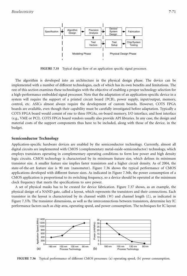
The algorithm is developed into an architecture in the physical design phase. The device can be
implemented with a number of different technologies, each of which has its own benefits and limitations. The
rest of this section examines these technologies with the objective of enabling a proper technology selection for
a high-performance embedded signal processor. Note that the adaptation of an application-specific device in a
system will require the support of a printed circuit board (PCB), power supply, input/output, memory,
control, etc. ASICs almost always require the development of custom boards. However, COTS FPGA
boards are available, even though their capability must be carefully investigated before adaptation. Typically a
COTS FPGA board would consist of one to three FPGAs, on-board memory, I/O interface, and host interface
(e.g., VME or PCI). COTS FPGA board vendors usually also provide API libraries. In any case, the design and
material costs of the support components thus have to be included, along with those of the device, in the
budget.
Semiconductor Technology
Application-specific hardware devices are enabled by the semiconductor technology. Currently, almost all
digital circuits are implemented with CMOS (complementary metal-oxide-semiconductor) technology, which
employs transistors operating in complementary operating conditions to form low power and high density
logic circuits. CMOS technology is characterized by its minimum feature size, which defines its minimum
transistor size. A smaller feature size implies faster transistors and a higher circuit density. As of 2004, the
state-of-the-art feature size is 90 nm (nanometer). Figure 7.36 shows the typical performance of CMOS
applications developed with different feature sizes. As indicated in Figure 7.36b, the power consumption of a
CMOS application is proportional to its switching frequency, so a device should be operated at the minimum
clock frequency that meets the specifications to save power.
A set of physical masks has to be created for device fabrication. Figure 7.37 shows, as an example, the
physical design of a NAND gate, called a layout, which represents the transistors and their connections. Each
transistor in the layout is characterized by its channel width (W) and channel length (L), as indicated in
Figure 7.37b. The transistor dimensions, as well as the interconnections between transistors, determine key IC
performance factors such as chip area, operating speed, and power consumption. The techniques for IC layout
SpecificationAlgorithmDesign
PrecisionAnalysis
Device/SystemDesign
Fabrication
TestVectors
TestSetup
Chip/SystemTesting
Modeling Phase Physical Design Phase
FIGURE 7.35 Typical design flow of an application specific signal processor.
0
200
400
600
800
1000
1200
1400
180 nm 150 nm 130 nm 90 nmProcess Technology
App
licat
ion
Spe
ed(M
Hz)
0
5
10
15
20
25
30
35
180 nm 150 nm 130 nm 90 nmProcess Technology
Pow
er(n
W/M
Hz)
(a) (b)
FIGURE 7.36 Typical performance of different CMOS processes: (a) operating speed, (b) power consumption.
7-71Bioelectricity

design and optimization are beyond the scope of this handbook, so interested readers are referred to Ref. [16]
for a more in-depth explanation of topics related to IC designs.
An embedded signal processor designer often has to balance between various competing objectives:
development cost, production cost, performance (operation speed and power consumption), time-to-market,
and volume expectation. It is very difficult, if not impossible, to optimize a design for all of these objectives.
The constraints specific to an application should be used to select from available implementation technologies,
which include full-custom ASICs, standard-cell ASICs, FPGAs, and structured ASICs.
Full-Custom ASIC
The layout of a module or even a complete IC can be manually created by specifying individual transistor
dimensions, locations, and their connections. This approach is commonly referred to as the full-custom
design. Potentially very high performance can be achieved in a full-custom design since the circuit is under the
direct control of the designer. However, the performance benefit comes at the price of an extremely high
design complexity. Usually, this design flow is only used to meet extremely high performance requirement
with a high volume production so that the non-recurring engineering (NRE) cost can be divided among a
large number of devices.
There are architectural properties that can be explored to facilitate a full-custom design. If a circuit has a
high degree of regularity, then only a few types of cells need to be crafted. Another useful property is local
communication between cells, which allows interconnections to be formed when cells are put together without
the need for explicit routing. Cells can then be assembled using a process called tessellation, which is similar to
laying the tiles on a bathroom wall.
Figure 7.38 shows the typical design flow of a full-custom ASIC. The layouts of the cells (i.e., building
blocks) are created. In order to verify the cells, layouts are converted into circuit schematic diagrams in a
process called extraction. The extracted schematics are compared to target schematics with a layout vs.
schematic (LVS) tool. The function and performance of the cells are determined by simulation. A tessellation
technique is used to assemble the cells into the final chip layout. The entire circuit is verified by LVS, design
rule check (DRC), electric rule check (ERC), and simulation before it is delivered to a silicon foundry for
AB Z
Vdd
Vss
A B
ZTransistor
Channel Length(L)
TransistorChannel Width(W)
Vdd
Vss
A BZ
(a) (b) (c)
FIGURE 7.37 NAND gate design: (a) symbol, (b) layout, (c) schematic diagram.
ArchitectureDesign
CellLayout
Extraction &Simulation
ChipLayout
Extraction &Simulation Tape-Out Testing
FIGURE 7.38 Full-custom ASIC design flow.
7-72 Sensors, Nanoscience, Biomedical Engineering, and Instruments

fabrication, which is commonly referred to as a tape-out. The ASICs are tested when they come back from the
silicon foundry.
Standard-Cell ASIC
With millions of transistors involved, it is extremely difficult to manually lay out an entire IC. Another
approach to creating an ASIC uses a library of basic building blocks, called standard cells. Standard-cell
libraries are commercially available for specific fabrication processes. A library usually contains primary logic
gates (e.g., inverter, NAND, NOR, etc.) as well as function blocks (e.g., adder, multiplier, memory, etc.). The
quality of a library is a significant determining factor of the design performance, so choosing a library is
critical to the success of a design.
A typical standard-cell ASIC design flow is shown in Figure 7.39. The device to be designed is described in a
hardware description language (HDL) program, which can be simulated for verification and synthesized into a
netlist of standard cells. Currently, the popular HDLs are (very high speed integrated circuit hardware
description language (VHDL) and Verilog, which are programming languages specially designed to allow the
description of circuits. However, SystemC, a language based on the context of Cþ and enhanced with a class
library of hardware-oriented constructs, is also gaining popularity. Advocates of SystemC claim that the use of
an HDL originated as a general programming language can facilitate the design and verification of a system
from concept to implementation in hardware and software.
The standard cells are then arranged on the available chip area with all the associated signals connected. The
task of arranging the cells on the layout, called the placement process, attempts to determine the best location
for each cell. The routing process takes the result of a placement and automatically completes the
interconnections. A chip level verification (LVS, DRC, ERC, etc.) is performed before a tape-out.
FPGA Design
While ASICs have the potential of achieving the highest performance offered by a semiconductor process, their
high design complexity (especially in the case of a full-custom design) and high fabrication cost often make
them cost prohibitive. FPGA-based designs are appropriate for applications that do not require ASIC-like
performance and can thereby benefit from much lower total development costs. As shown in the conceptual
architecture of Figure 7.40, an FPGA is a fully manufactured device that contains an array of configurable logic
blocks, memory blocks, arithmetic blocks, and interconnects that are designer controllable. Advanced FPGAs
may have microprocessor hard cores embedded to implement functions that are more suitable for a
programmable processor than a dedicated circuit, such as a controller. Alternatively, microprocessor soft cores
are also available.
HardwareDescriptionLanguage
Simulation &Synthesis
Place &Route Verification
Extraction &Simulation Tape-Out Testing
FIGURE 7.39 Standard-cell ASIC design flow.
FIGURE 7.40 Conceptual FPGA architecture.
7-73Bioelectricity

The FPGA design flow is shown in Figure 7.41. Similar to the standard-cell ASIC design flow, a HDL
program describing the circuit is created for simulation and synthesis. The resultant netlist is mapped, placed,
and routed to create configuration data, which contain the information needed to configure the FPGA into an
application-specific design.
There are three types of FPGAs. SRAM (static random access memory)-based FPGAs store configuration
data in SRAMs so they are reprogrammable. However, the configuration is volatile since they are lost when the
power is off. Anti-fuse-based FPGAs are one-time programmable and nonvolatile. Flash-based FPGAs use flash
memories and are both reprogrammable and nonvolatile.
An FPGA is a good implementation platform for prototyping and low volume production. When the
volume of a product warrants, it may be desirable to take an FPGA design and convert it into an ASIC. The
most common reason for FPGA-to-ASIC conversion is to get better speed and lower power consumption since
FPGAs are significantly more power hungry than their ASIC counterparts. While theoretically, the HDL
program originally designed for an FPGA can be re-synthesized into a standard-cell ASIC, in reality, the design
effort is close to a new design cycle. The re-synthesizing effort can be facilitated by targeting a gate-array style
architecture designed to somewhat mimic an FPGA structure.
One approach for FPGA-to-ASIC conversion is to use a mask-programmed device with the same
architecture as the FPGA to be replaced. Improved performance is a direct result of replacing programmable
routing connections with metal customization. This approach has the advantage that the original FPGA
designed for prototyping and early production can be extended into an ASIC without modifications. However,
this is an FPGA-vendor-supplied solution.
Structured ASIC
A new kind of semi-custom mask-programmable device, the structured ASIC, can be viewed as a technology
located on the spectrum between FPGAs and ASICs. The structured ASIC appears to have the potential to
achieve close to ASIC level performance without high non recurring engineering (NRE) costs, long design
cycles, and high risk factors. Structured ASIC devices typically provide pre-manufactured logic components,
routing fabric and a number of commonly used functional blocks (e.g., high-speed I/O, memory,
microprocessors, etc.). The devices are manufactured except for a few metal layers, which are used to
customize the final devices for a specific design.
The advantages of a structured ASIC over an ASIC are lower design, manufacturing, testing, and integration
costs. Compared with FPGAs, structured ASICs offer higher performance with lower power consumption and
a smaller footprint.
Intellectual Property
Design reuse contributes to both risk mitigation and a reduction in development time. The most direct use of
this principle is the use of functions from a previous product. The intellectual property (IP) core approach
extends the concept to the use of functions designed by another party. IP cores are available for a large variety
of functions, ranging from adders to microprocessors.
There are three types of IP cores: soft, firm, and hard. A soft IP core is represented with HDL at the register
transfer level (RTL). Users will be required to perform the typical steps (synthesis, place and route, and
verification) in the design flow following HDL development. Since the IP representation is provided in HDL, it
is relatively technology independent. A firm IP core moves a bit closer to the physical side by delivering the IP
design in a netlist of generic logic cells. No synthesis is required. The responsibility of the user is to perform the
HardwareDescriptionLanguage
Simulation &Synthesis
Map, Place &Route Testing
FIGURE 7.41 FPGA design flow.
7-74 Sensors, Nanoscience, Biomedical Engineering, and Instruments
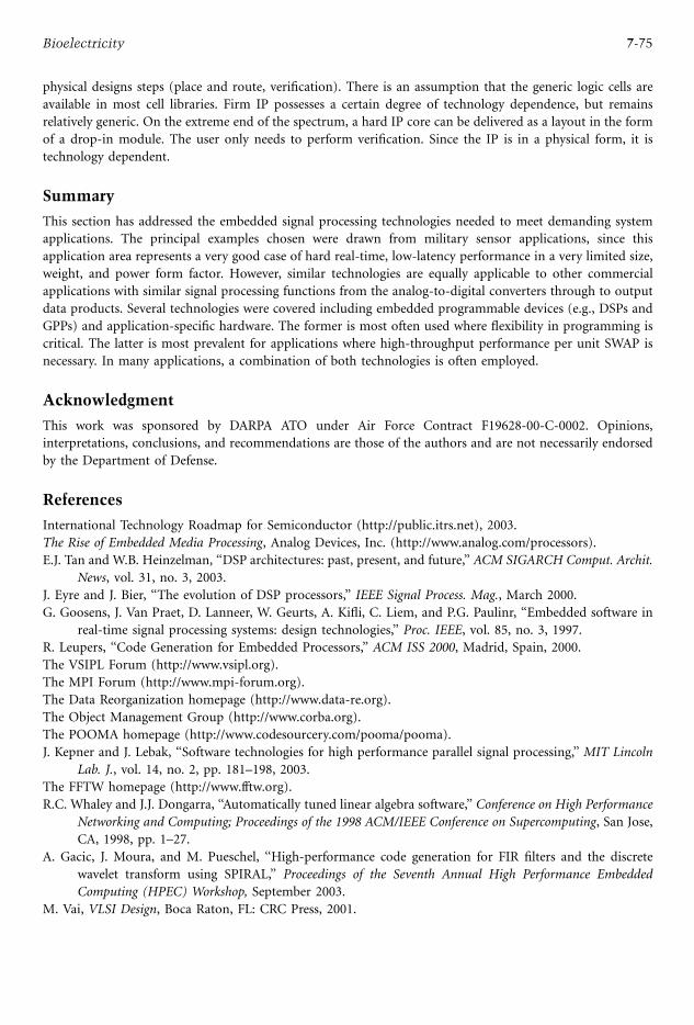
physical designs steps (place and route, verification). There is an assumption that the generic logic cells are
available in most cell libraries. Firm IP possesses a certain degree of technology dependence, but remains
relatively generic. On the extreme end of the spectrum, a hard IP core can be delivered as a layout in the form
of a drop-in module. The user only needs to perform verification. Since the IP is in a physical form, it is
technology dependent.
Summary
This section has addressed the embedded signal processing technologies needed to meet demanding system
applications. The principal examples chosen were drawn from military sensor applications, since this
application area represents a very good case of hard real-time, low-latency performance in a very limited size,
weight, and power form factor. However, similar technologies are equally applicable to other commercial
applications with similar signal processing functions from the analog-to-digital converters through to output
data products. Several technologies were covered including embedded programmable devices (e.g., DSPs and
GPPs) and application-specific hardware. The former is most often used where flexibility in programming is
critical. The latter is most prevalent for applications where high-throughput performance per unit SWAP is
necessary. In many applications, a combination of both technologies is often employed.
Acknowledgment
This work was sponsored by DARPA ATO under Air Force Contract F19628-00-C-0002. Opinions,
interpretations, conclusions, and recommendations are those of the authors and are not necessarily endorsed
by the Department of Defense.
References
International Technology Roadmap for Semiconductor (http://public.itrs.net), 2003.
The Rise of Embedded Media Processing, Analog Devices, Inc. (http://www.analog.com/processors).
E.J. Tan and W.B. Heinzelman, ‘‘DSP architectures: past, present, and future,’’ ACM SIGARCH Comput. Archit.
News, vol. 31, no. 3, 2003.
J. Eyre and J. Bier, ‘‘The evolution of DSP processors,’’ IEEE Signal Process. Mag., March 2000.
G. Goosens, J. Van Praet, D. Lanneer, W. Geurts, A. Kifli, C. Liem, and P.G. Paulinr, ‘‘Embedded software in
real-time signal processing systems: design technologies,’’ Proc. IEEE, vol. 85, no. 3, 1997.
R. Leupers, ‘‘Code Generation for Embedded Processors,’’ ACM ISS 2000, Madrid, Spain, 2000.
The VSIPL Forum (http://www.vsipl.org).
The MPI Forum (http://www.mpi-forum.org).
The Data Reorganization homepage (http://www.data-re.org).
The Object Management Group (http://www.corba.org).
The POOMA homepage (http://www.codesourcery.com/pooma/pooma).
J. Kepner and J. Lebak, ‘‘Software technologies for high performance parallel signal processing,’’ MIT Lincoln
Lab. J., vol. 14, no. 2, pp. 181–198, 2003.
The FFTW homepage (http://www.fftw.org).
R.C. Whaley and J.J. Dongarra, ‘‘Automatically tuned linear algebra software,’’ Conference on High Performance
Networking and Computing; Proceedings of the 1998 ACM/IEEE Conference on Supercomputing, San Jose,
CA, 1998, pp. 1–27.
A. Gacic, J. Moura, and M. Pueschel, ‘‘High-performance code generation for FIR filters and the discrete
wavelet transform using SPIRAL,’’ Proceedings of the Seventh Annual High Performance Embedded
Computing (HPEC) Workshop, September 2003.
M. Vai, VLSI Design, Boca Raton, FL: CRC Press, 2001.
7-75Bioelectricity

Credits
Figure 7.29 courtesy of Xilinx Inc. and Annapolis Micro Systems, Inc. Xilinx and Virtex wordmarks and
logomarks are registered trademarks protected by copyright. With permission.
Figure 7.30 courtesy of Xilinx Inc. and Mercury Computer Systems, Inc. Xilinx and Virtex wordmarks and
logomarks are registered trademarks protected by copyright. With permission.
Figure 7.32 courtesy of Mercury Computer Systems, Inc. With permission.
7-76 Sensors, Nanoscience, Biomedical Engineering, and Instruments

8Biomedical Sensors
Michael R. NeumanMichigan Technological University
8.1 Introduction ........................................................................ 8-1
8.2 Physical Sensors.................................................................... 8-2
8.3 Chemical Sensors .................................................................. 8-6
8.4 Bioanalytical Sensors ............................................................. 8-9
8.5 Applications ....................................................................... 8-10
8.1 Introduction
Any instrumentation system can be described as having three fundamental components: a sensor, a signal
processor, and a display and/or storage device. Although all these components of the instrumentation system
are important, the sensor serves a special function in that it interfaces the instrument with the system being
measured. In the case of biomedical instrumentation, a biomedical sensor (which in some cases may be referred
to as a biosensor) is the interface between the electronic instrument and the biological system. There are some
general concerns that are important for any sensor in an instrumentation system regarding its ability to
effectively carry out the interface function. These concerns are especially important for biomedical sensors
because the sensor can affect the system being measured and the system can affect the sensor. Sensors must be
designed so that they minimize their interaction with the biological host. It is important that the presence of the
sensor does not affect the variable being measured in the vicinity of the sensor via interaction between the sensor
and the biologic system. If the sensor is placed in a living organism, that organismwill probably recognize it as a
foreign body and react to it. This may change the quantity being sensed in the vicinity of the sensor so that the
measurement reflects a reaction to the foreign body rather than a central characteristic of the host.
Similarly, the biological system can affect the performance of the sensor. The foreign body reaction might
cause the host’s system to attempt to break down the materials of the sensor in order to remove it. This may, in
fact, degrade the sensor package so that it can no longer perform in an adequate manner. Even if the foreign
body reaction is not strong enough to affect the measurement, just the fact that the sensor is in a warm,
aqueous environment may cause water to eventually invade the package and degrade its function. Finally, as
will be described below, sensors that are implanted in the body are not accessible for calibration. Thus, they
must have extremely stable characteristics so that frequent calibrations are not necessary.
Biomedical sensors can be classified according to how they are used with respect to the biological system.
Table 8.1 shows that sensors can range from noninvasive to invasive as far as the biological host is concerned.
The most noninvasive of biomedical sensors do not even contact the biological system being measured.
Sensors of radiant heat or sound energy coming from an organism are examples of noncontacting sensors.
Noninvasive sensors can also be placed on the body surface. Skin surface thermometers, biopotential electrodes,
and strain gauges placed on the skin are examples of noninvasive sensors. Indwelling sensors are those that can be
placed into a natural body cavity that communicates with the outside. These are sometimes referred to as
minimally invasive sensors and include such familiar sensors as oral–rectal thermometers, intrauterine pressure
transducers, and stomach pH sensors. The most invasive sensors are those that need to be surgically placed and
8-1

that require some tissue damage associated with their installation. A needle electrode for picking up
electromyographic signals directly frommuscles; a blood pressure sensor placed in an artery, vein, or in the heart
itself; or a blood flow transducer positioned on a major artery are all examples of invasive sensors.
We can also classify sensors in terms of the quantities that they measure. Physical sensors are used in
measuring physical quantities such as displacement, pressure, and flow, while chemical sensors are used to
determine the concentration of chemical substances within the host. A sub-group of the chemical sensors that
are concerned with sensing the presence and the concentration of biochemical materials in the host are known
as bioanalytical sensors or biosensors.
In the following paragraphs we will look at each type of sensor and present some examples as well as
describe some of the important issues surrounding these types of sensors.
8.2 Physical Sensors
Physical variables associated with biomedical systems are measured by a group
of sensors known as physical sensors. A list of typical variables measured by
these devices and examples of sensors used to measure them are given in
Table 8.2. These quantities are similar to physical quantities measured by
sensors for nonbiomedical applications, and the devices used for biomedical
and nonbiomedical sensing are, therefore, quite similar. There are, however,
two principal exceptions: pressure and flow sensors. Themeasurement of blood
or other fluid pressure and flow in humans and other animals is problematic.
Direct pressure measurement refers to the evaluation of the pressure using a
sensor that is in contact with the blood or another fluid being measured, or
contacts it through an intermediate fluid such as a physiologic saline solution.
Direct pressure sensors are invasive in that there needs to be a physical
connection between the sensor and the circulating blood or fluid being
measured. This means that a needle or surgical approach to the fluid compartment being measured is necessary.
Indirect pressure measurement involves a sensor that does not actually contact the fluid being measured. An
indirect pressure sensor measures a quantity, such as the tension in a vessel wall, that is related to the desired
pressure and allows the sensor to be separated from the fluid beingmeasured. Themost familiar indirect pressure
measurement involves the determination of arterial blood pressure using a sphygmomanometer cuff. This is the
method that is usually used inmedical examinations. It is a noninvasive instrument and themeasurement is easily
performed. Often, however, it is less accurate than the direct measure of blood pressure, and it provides only a
sample in time rather than a continuous record as is possible with the direct measurement technique.
Until recently, the primary sensor used for direct blood pressure measurement was the unbonded strain
gauge pressure transducer shown in Figure 8.1. The basic principle of this device is that a differential pressure
seen across a diaphragm will cause that diaphragm to deflect. This deflection is then measured by a
displacement transducer. In the unbonded strain gauge sensor a closed chamber is covered by a flexible
diaphragm. This diaphragm is attached to a structure that has four fine-gauge wires drawn between it and the
chamber walls. A dome with the appropriate hardware for fluid coupling to a pressure source covers
the diaphragm on the side opposite the chamber and wires such that when the pressure in the dome exceeds
the pressure in the chamber, the diaphragm is deflected into the chamber. This causes two of the fine wires to
TABLE 8.2 Physical Variables
Measured by Biomedical Sensors
Displacement (linear and angular)
Velocity
Acceleration
Temperature
Force (torque, weight, and mass)
Pressure
Sound
Flow
Radiant energy
TABLE 8.1 Classification of Biomedical Sensors According
to Their Interface with the Biologic Host
Degree of Invasion Sensor Classification
Isolated Noncontacting
Noninvasive Body surface
Minimally invasive Indwelling
Invasive Implanted
8-2 Sensors, Nanoscience, Biomedical Engineering, and Instruments
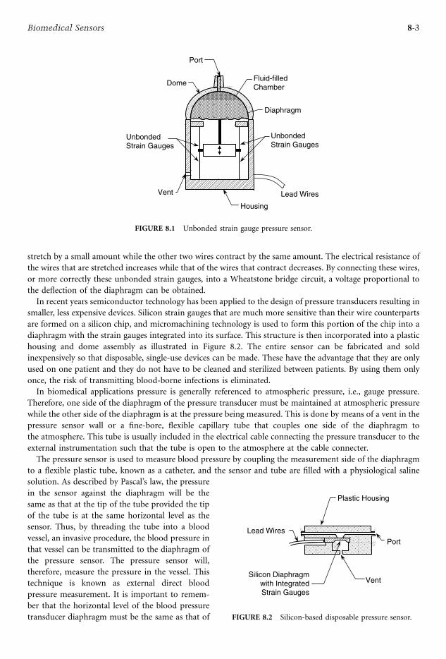
stretch by a small amount while the other two wires contract by the same amount. The electrical resistance of
the wires that are stretched increases while that of the wires that contract decreases. By connecting these wires,
or more correctly these unbonded strain gauges, into a Wheatstone bridge circuit, a voltage proportional to
the deflection of the diaphragm can be obtained.
In recent years semiconductor technology has been applied to the design of pressure transducers resulting in
smaller, less expensive devices. Silicon strain gauges that are much more sensitive than their wire counterparts
are formed on a silicon chip, and micromachining technology is used to form this portion of the chip into a
diaphragm with the strain gauges integrated into its surface. This structure is then incorporated into a plastic
housing and dome assembly as illustrated in Figure 8.2. The entire sensor can be fabricated and sold
inexpensively so that disposable, single-use devices can be made. These have the advantage that they are only
used on one patient and they do not have to be cleaned and sterilized between patients. By using them only
once, the risk of transmitting blood-borne infections is eliminated.
In biomedical applications pressure is generally referenced to atmospheric pressure, i.e., gauge pressure.
Therefore, one side of the diaphragm of the pressure transducer must be maintained at atmospheric pressure
while the other side of the diaphragm is at the pressure being measured. This is done by means of a vent in the
pressure sensor wall or a fine-bore, flexible capillary tube that couples one side of the diaphragm to
the atmosphere. This tube is usually included in the electrical cable connecting the pressure transducer to the
external instrumentation such that the tube is open to the atmosphere at the cable connecter.
The pressure sensor is used to measure blood pressure by coupling the measurement side of the diaphragm
to a flexible plastic tube, known as a catheter, and the sensor and tube are filled with a physiological saline
solution. As described by Pascal’s law, the pressure
in the sensor against the diaphragm will be the
same as that at the tip of the tube provided the tip
of the tube is at the same horizontal level as the
sensor. Thus, by threading the tube into a blood
vessel, an invasive procedure, the blood pressure in
that vessel can be transmitted to the diaphragm of
the pressure sensor. The pressure sensor will,
therefore, measure the pressure in the vessel. This
technique is known as external direct blood
pressure measurement. It is important to remem-
ber that the horizontal level of the blood pressure
transducer diaphragm must be the same as that of
Vent
Fluid-filledChamber
Housing
Diaphragm
Lead Wires
Port
Dome
UnbondedStrain Gauges
UnbondedStrain Gauges
FIGURE 8.1 Unbonded strain gauge pressure sensor.
Vent
Plastic Housing
Silicon Diaphragmwith IntegratedStrain Gauges
Lead Wires
Port
FIGURE 8.2 Silicon-based disposable pressure sensor.
8-3Biomedical Sensors
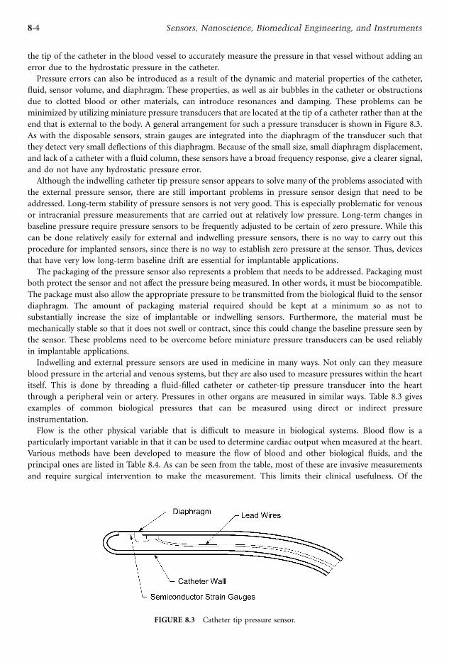
the tip of the catheter in the blood vessel to accurately measure the pressure in that vessel without adding an
error due to the hydrostatic pressure in the catheter.
Pressure errors can also be introduced as a result of the dynamic and material properties of the catheter,
fluid, sensor volume, and diaphragm. These properties, as well as air bubbles in the catheter or obstructions
due to clotted blood or other materials, can introduce resonances and damping. These problems can be
minimized by utilizing miniature pressure transducers that are located at the tip of a catheter rather than at the
end that is external to the body. A general arrangement for such a pressure transducer is shown in Figure 8.3.
As with the disposable sensors, strain gauges are integrated into the diaphragm of the transducer such that
they detect very small deflections of this diaphragm. Because of the small size, small diaphragm displacement,
and lack of a catheter with a fluid column, these sensors have a broad frequency response, give a clearer signal,
and do not have any hydrostatic pressure error.
Although the indwelling catheter tip pressure sensor appears to solve many of the problems associated with
the external pressure sensor, there are still important problems in pressure sensor design that need to be
addressed. Long-term stability of pressure sensors is not very good. This is especially problematic for venous
or intracranial pressure measurements that are carried out at relatively low pressure. Long-term changes in
baseline pressure require pressure sensors to be frequently adjusted to be certain of zero pressure. While this
can be done relatively easily for external and indwelling pressure sensors, there is no way to carry out this
procedure for implanted sensors, since there is no way to establish zero pressure at the sensor. Thus, devices
that have very low long-term baseline drift are essential for implantable applications.
The packaging of the pressure sensor also represents a problem that needs to be addressed. Packaging must
both protect the sensor and not affect the pressure being measured. In other words, it must be biocompatible.
The package must also allow the appropriate pressure to be transmitted from the biological fluid to the sensor
diaphragm. The amount of packaging material required should be kept at a minimum so as not to
substantially increase the size of implantable or indwelling sensors. Furthermore, the material must be
mechanically stable so that it does not swell or contract, since this could change the baseline pressure seen by
the sensor. These problems need to be overcome before miniature pressure transducers can be used reliably
in implantable applications.
Indwelling and external pressure sensors are used in medicine in many ways. Not only can they measure
blood pressure in the arterial and venous systems, but they are also used to measure pressures within the heart
itself. This is done by threading a fluid-filled catheter or catheter-tip pressure transducer into the heart
through a peripheral vein or artery. Pressures in other organs are measured in similar ways. Table 8.3 gives
examples of common biological pressures that can be measured using direct or indirect pressure
instrumentation.
Flow is the other physical variable that is difficult to measure in biological systems. Blood flow is a
particularly important variable in that it can be used to determine cardiac output when measured at the heart.
Various methods have been developed to measure the flow of blood and other biological fluids, and the
principal ones are listed in Table 8.4. As can be seen from the table, most of these are invasive measurements
and require surgical intervention to make the measurement. This limits their clinical usefulness. Of the
FIGURE 8.3 Catheter tip pressure sensor.
8-4 Sensors, Nanoscience, Biomedical Engineering, and Instruments

invasive blood flow sensors, some must be placed around an artery or vein to make a measurement, and this
requires significant surgical intervention and subject recovery. Other sensors placed on a catheter can be
introduced into the body by accessing a peripheral artery or vein and threading in the catheter to get the
sensor to the point in the vessel where the measurement is to be made. This still involves an invasive surgical
procedure, but the trauma can be minimized, and this can reduce the effect that the surgical procedure has on
the variable being measured.
The most commonly used types of invasive blood flow sensors are the electromagnetic flowmeter and the
Doppler ultrasonic flowmeter. The fundamental principles of each are based on a characteristic property of the
blood. In the former case, the fact that blood contains ions, among other components, and in the latter case
that the blood contains cells that are large enough to scatter and reflect ultrasonic waves. The basic form of an
electromagnetic flowmeter is illustrated in Figure 8.4. Because the blood flowing in the vessel contains ions,
they will be moving with the blood at a velocity corresponding to the flow. When they pass the region of the
vessel where the magnetic field from the external (to the vessel) magnet is situated, positive ions will
experience a deflecting force perpendicular to both the direction of the ion movement and the direction of the
magnetic field. Negative ions in the blood will experience a deflecting force in the opposite direction. In both
TABLE 8.3 Biologic Pressures that Can Be Measured Using Direct or Indirect Pressure Sensors
Anatomic Structure Pressure Signal Direct Sensor Indirect Sensor
Artery Arterial blood pressure Fluid-filled catheter with
external pressure sensor
Catheter tip sensor
Sphygmomanometer
Tonometer
Vein Venous blood pressure Fluid-filled catheter with external
pressure sensor
No method
Heart Intracardiac pressure Fluid-filled catheter with external
pressure sensor
No method
Urinary bladder Cystometric pressure Catheter tip sensor No method
Eye Intraocular pressure Intraocular sensor Tonometer
Stomach Intragastric pressure Balloon-tipped catheter
Catheter tip sensor
No method
Brain Intracranial pressure Fluid-filled catheter with
external pressure sensor
Intracranial sensor
Tonometer (newborn
infants only)
Spinal cord Cerebral–spinal fluid
pressure
Fluid-filled catheter with external
pressure sensor
No method
TABLE 8.4 Methods to Measure Fluid Flow in the Body
Flow Measurement
Method
Example Biomedical
Application Degree of Invasion Type of Measurement
Fick principle Cardiac output Non- or minimally
invasive
Sampled
Indicator dilution Cardiac output Minimally invasive Sampled
Electromagnetic flowmeter Arterial or venous
blood flow
Invasive Continuous
Ultrasonic Doppler flowmeter Arterial or venous
blood flow
Invasive Continuous
Pulsed Doppler ultrasound Arterial or venous
blood flow combined
with imaging
Noninvasive Rapid sampled, essentially
continuous
Magnetic resonance imaging Tissue perfusion
combined with
imaging
Noninvasive Rapid sampled, essentially
continuous
8-5Biomedical Sensors

cases the magnitude of the deflecting force will be proportional to the magnetic field strength and the velocity
of the blood, and so the actual deflection of these ions will be proportional to the blood velocity when the
magnetic field is uniform and of constant magnitude. Thus, if we put a pair of electrodes on the vessel wall
along the axis of these deflecting forces, we should see a potential difference due to the deflection of these ions.
This potential difference will be proportional to the blood velocity. Blood volume flow can be determined
from this by knowing the cross-sectional area of the flowing column of blood either by measuring the vessel
inner diameter or by constraining the vessel to have a fixed inner diameter by putting a fixed cuff around it.
Ultrasonic flowmeters are based on the interaction of ultrasonic waves with the flowing blood. Ultrasonic
energy in the megahertz range is readily scattered and reflected by the blood cells. Thus, if the cells reflecting
the ultrasonic energy are moving, the reflected energy will be shifted in frequency in proportion to the velocity
of these cells according to the Doppler effect. By measuring this frequency shift, one can determine the relative
velocity of the cells and, hence, the velocity of the blood. If the angle of the ultrasonic wave propagation
direction with respect to the direction of the blood cells’ velocity vector is known, one can quantitatively
determine the blood velocity from the Doppler frequency shift. It is then possible to use the same approach as
described for the electromagnetic blood flowmeter to determine the volume blood flow from the blood
velocity.
Ultrasound is also used to estimate blood flow noninvasively. An ultrasonic beam can be introduced into
the body from a transducer on its surface, and the same transducer can receive the reflected signal from the
flowing blood. The extent of the Doppler shift will be proportional to the blood velocity of the vessel being
illuminated by the ultrasonic beam. Clinical instruments combine this mode of operation with ultrasonic
imaging to show images of the anatomic structures surrounding the vessels being studied, with a color display
within the vessel where the color represents the velocity of the blood. This technique is especially useful in
observing partial obstruction and turbulence within blood vessels.
8.3 Chemical Sensors
There are many biomedical situations where it is necessary to know the concentration or chemical activity of a
particular substance in a biological sample. Chemical sensors provide the interface between an instrument and
the specimen to allow one to determine these quantities. These sensors can be used on a biological specimen
taken from the host and tested in a laboratory, or they can be used for in vivo measurements either as
noninvasive or invasive sensors. There are many types of chemical sensors used in biomedical
instrumentation. Table 8.5 lists some general categories of sensors. Electrochemical and optical sensors are
most frequently used for biomedical measurements both in vivo and in vitro. An example of an
v
Magnet
B
u
Electrode
Electrode
Vessel
FIGURE 8.4 Basic structure of an electromagnetic flow sensor.
8-6 Sensors, Nanoscience, Biomedical Engineering, and Instruments
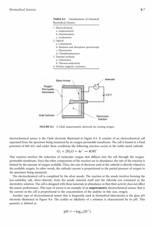
electrochemical sensor is the Clark electrode illustrated in Figure 8.5. It consists of an electrochemical cell
separated from the specimen being measured by an oxygen-permeable membrane. The cell is biased at a fixed
potential of 600 mV, and under these conditions the following reaction occurs at the noble metal cathode:
O2 þ 2H2O ¼ 4e ! 4OH
This reaction involves the reduction of molecular oxygen that diffuses into the cell through the oxygen-
permeable membrane. Since the other components of the reaction are in abundance, the rate of the reaction is
limited by the amount of oxygen available. Thus, the rate of electrons used at the cathode is directly related to
the available oxygen. In other words, the cathode current is proportional to the partial pressure of oxygen in
the specimen being measured.
The electrochemical cell is completed by the silver anode. The reaction at the anode involves forming the
low-solubility salt, silver-chloride, from the anode material itself and the chloride ion contained in the
electrolytic solution. The cell is designed with these materials in abundance so that their activity does not affect
the sensor performance. This type of sensor is an example of an amperometric electrochemical sensor, that is
the current in the cell is proportional to the concentration of the analyte; in this case, oxygen.
Another type of electrochemical sensor that is frequently used in biomedical laboratories is the glass pH
electrode illustrated in Figure 8.6. The acidity or alkalinity of a solution is characterized by its pH. This
quantity is defined as
pH ¼ log10 ½Hþ
TABLE 8.5 Classifications of Chemical
Biomedical Sensors
1. Electrochemical
a. Amperometric
b. Potentiometric
c. Coulometric
2. Optical
a. Colorimetric
b. Emission and absorption spectroscopy
c. Fluorescence
d. Chemiluminescence
3. Thermal methods
a. Calorimetry
b. Thermoconductivity
4. Nuclear magnetic resonance
FIGURE 8.5 A Clark amperometric electrode for sensing oxygen.
8-7Biomedical Sensors

where [Hþ] is the activity of the hydrogen ions in solution, a quantity that is related to the concentration ofthe hydrogen ions. This sensor only works in an aqueous environment. It consists of an inner chamber
containing an electrolytic solution of known pH and an outer solution with an unknown pH that is to be
measured. The membrane consists of a specially formulated glass that appears to allow hydrogen ions to pass
in either direction but will not pass other chemical species. In practice, the processes in this glass membrane
and on its surfaces are much more complicated, but the above description is adequate to understand the
fundamental operation of a glass pH electrode. If the concentration of hydrogen ions in the external solution is
greater than that in the internal solution, there will be a gradient that appears to force hydrogen ions to diffuse
through the membrane into the internal solution. This will cause the internal solution side of the membrane
to have a greater positive charge than the external solution side, so that an electrical potential and, hence, an
electric field will exist across the membrane. This field will counteract the diffusion of hydrogen ions due to the
concentration difference and equilibrium will eventually be established. The potential across the membrane at
this equilibrium condition will be related to the hydrogen ion concentration difference (or more accurately, the
activity difference) between the inner and outer solutions. This potential is given by the Nernst equation:
E ¼ RT
nFln
a1a2
where E is the potential measured, R is the universal gas constant, T is the absolute temperature, n is the
valence of the ion, and a1 and a2 are the activities of the ions on each side of the membrane. Thus, the
potential measured across the glass membrane will be proportional to the pH of the solution being studied. At
room temperature the sensitivity of the electrode is approximately 60 mV/pH. It is not practical to measure
the potential across the membrane directly, so reference electrodes, sensors that can be used to measure
electrical potential of an electrolytic solution, are used to contact the solution on either side of the membrane
to measure the potential difference across it. The reference electrodes and the glass membrane are incorporated
into the structure shown in Figure 8.6 which is known as a glass pH electrode. This is an example of a
potentiometric measurement made using an ion-selective membrane because the sensor potential is
proportional to the logarithm of the activity difference of the analyte across the analyte-selective membrane.
There are other types of ion-selective membrane potentiometric chemical sensors that are used for
biomedical applications. The membranes of these sensors determine the ion being sensed. The membrane can
be based upon glass or a highly plasticized polymeric material such as polyvinyl chloride, but the key
component is the substance that is added to the membrane that allows it to appear to selectively pass a
single ion.
FIGURE 8.6 A glass electrode pH sensor.
8-8 Sensors, Nanoscience, Biomedical Engineering, and Instruments
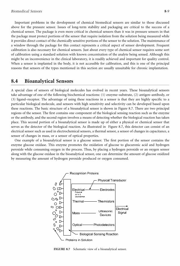
Important problems in the development of chemical biomedical sensors are similar to those discussed
above for the pressure sensor. Issues of long-term stability and packaging are critical to the success of a
chemical sensor. The package is even more critical in chemical sensors than it was in pressure sensors in that
the package must protect portions of the sensor that require isolation from the solution being measured while
it provides direct contact of the chemically sensitive portions of the sensor to the solution. The maintenance of
a window through the package for this contact represents a critical aspect of sensor development. Frequent
calibration is also necessary for chemical sensors. Just about every type of chemical sensor requires some sort
of calibration using a standard solution with known concentration of the analyte being sensed. Although this
might be an inconvenience in the clinical laboratory, it is readily achieved and important for quality control.
When a sensor is implanted in the body, it is not accessible for calibration, and this is one of the principal
reasons that sensors of the types mentioned in this section are usually unsuitable for chronic implantation.
8.4 Bioanalytical Sensors
A special class of sensors of biological molecules has evolved in recent years. These bioanalytical sensors
take advantage of one of the following biochemical reactions: (1) enzyme–substrate, (2) antigen–antibody, or
(3) ligand–receptor. The advantage of using these reactions in a sensor is that they are highly specific to a
particular biological molecule, and sensors with high sensitivity and selectivity can be developed based upon
these reactions. The basic structure of a bioanalytical sensor is shown in Figure 8.7. There are two principal
regions of the sensor. The first contains one component of the biological sensing reaction such as the enzyme
or the antibody, and the second region involves a means of detecting whether the biological reaction has taken
place. This second portion of a bioanalytical sensor is made up of either a physical or chemical sensor that
serves as the detector of the biological reaction. As illustrated in Figure 8.7, this detector can consist of an
electrical sensor such as used in electrochemical sensors, a thermal sensor, a sensor of changes in capacitance, a
sensor of changes in mass, or a sensor of optical properties.
One example of a bioanalytical sensor is a glucose sensor. The first portion of the sensor contains the
enzyme glucose oxidase. This enzyme promotes the oxidation of glucose to glucuronic acid and hydrogen
peroxide while consuming oxygen in the process. Thus, by placing a hydrogen peroxide or an oxygen sensor
along with the glucose oxidase in the bioanalytical sensor, one can determine the amount of glucose oxidized
by measuring the amount of hydrogen peroxide produced or oxygen consumed.
FIGURE 8.7 Schematic view of a bioanalytical sensor.
8-9Biomedical Sensors

Stability is important for bioanalytical sensors, especially those that are used for long-term measurements.
Not only are the stability issues the same as for the physical and chemical sensors, but they are also related to
preservation of the biological molecules used in the first portion of the sensor. These molecules can often be
degraded or destroyed by heat or exposure to light. Even aging can degrade some of these molecules. Thus, an
important issue in dealing with bioanalytical sensors is the preservation of the biochemical components of the
sensor.
8.5 Applications
Biomedical sensors and instrumentation are used in biomedical research and patient care applications. In
terms of patient care, sensors are used as a part of instruments that carry out patient screening by making
measurements such as blood pressure using automated or manually operated apparatus. Specimen analysis is
another important application of biomedical sensors in patient care. This can include analyses that can be
carried out by the patients themselves in their homes such as is done with home blood glucose analyzers.
Instrumentation based upon biomedical sensors also can be used in the physician’s office for carrying out
some chemical analyses of patient specimens such as urinalysis or elementary blood chemistries such as serum
glucose and electrolytes. Sensors also are a part of large, multi-component, automatic blood analyzers used in
the central clinical laboratories of medical centers. Another application for biomedical sensors is in patient
monitoring. Sensors represent the front end of critical care monitors used in the intensive care unit and in the
operating and recovery rooms. Measurements cover a wide range of biomedical variables such as continuous
recordings of blood pressure and oxygen saturation of the arterial blood. The performance of these
instruments is strongly dependent on biomedical sensors. Patient monitoring can also be carried out in the
various clinical units of the hospital. Devices such as ambulatory cardiac monitors that allow patients to be
observed while they are free to move around on the ward are becoming important for clinical care in ‘‘step-
down’’ units for patients who have completed their stay in the intensive care unit. Patient monitoring has even
made its way into the home. Home cardiorespiratory monitors have been used with patients immediately after
discharge from the hospital to follow them in the critical first few days at home. The availability of this
technology makes it possible to discharge patients earlier, thereby helping to reduce healthcare costs while still
maintaining high quality medical care.
Summary
Sensors serve an important function in biomedical instrumentation systems in that they provide the interface
between the electronic instrument and the biological system being measured. Very often the quality of the
instrument is based upon the quality of the sensor at the instrument’s front end. Although electronic signal
processing has been developed to a high level, the signals are no better than the quality of the sensors that
provide them. Even though there have been many advances in biomedical sensor technology, many problems
remain to be overcome. Biomedical sensors will continue to be an important area for research and
development in biomedical engineering.
Defining Terms
Amperometric sensor: An electrochemical sensor that determines the amount of a substance by means of
an oxidation-reduction reaction involving that substance. Electrons are transferred as a part of the
reaction, so that the electrical current through the sensor is related to the amount of the substance seen
by the sensor.
Analyte: The substance being measured by a chemical or bioanalytical sensor and instrumentation system.
Bioanalytical sensor: A special case of a chemical sensor that determines the amount of a biochemical
substance. This type of sensor usually makes use of one of the following types of biochemical reactions:
enzyme–substrate, antigen–antibody, or ligand–receptor.
8-10 Sensors, Nanoscience, Biomedical Engineering, and Instruments

Biomedical sensor: A device for interfacing an instrumentation system with a biological system such as a
biological specimen or an entire organism. The device serves the function of detecting and measuring in
a quantitative fashion a physiological property of the biologic system.
Chemical sensor: The interface device for an instrumentation system that determines the concentration of
a chemical substance.
Noninvasive sensor: The interface device of an instrumentation system that measures a physiologic
variable from an organism without interrupting the integrity of that organism. This device can be in
direct contact with the surface of the organism or it can measure the physiologic quantity while
remaining remote from the organism.
Physical sensor: An interface device at the input of an instrumentation system that quantitatively measures
a physical quantity such as pressure or temperature.
Potentiometric sensor: A chemical sensor that measures the concentration or activity of a substance by
determining an electrical potential.
References
R.S.C. Cobbold, Transducers for Biomedical Measurements: Principles and Applications, New York: Wiley, 1974.
D.G. Fleming, W.H. Ko, and M.R. Neuman, Eds., Indwelling and Implantable Pressure Transducers, Cleveland,
OH: CRC Press, 1977.
L.A. Geddes, The Direct and Indirect Measurement of Blood Pressure, Chicago, IL: Year Book Medical
Publishers, 1970.
Jacob Fraden, Handbook of Modern Sensors: Physics, Designs, and Applications, 3rd ed., Berlin: Springer, 2004.
W. Gopel, J. Hesse, and J.N. Zemel, Sensors; A Comprehensive Survey, Weinheim, Germany: VCH
Verlagsgesellschaft, 1989.
J. Janata, Principles of Chemical Sensors, New York: Plenum Press, 1989.
R. Pallas-Areny and J.G. Webster, Sensors and Signal Conditioning, 2nd ed., New York: Wiley, 2001.
Tatsuo Togawa; Toshiyo Tamura; P. Ake Oberg, Biomedical Transducers and Instruments, Boca Raton, FL: CRC
Press, 1997.
B.R. Eggins, Chemical Sensors and Biosensors (Analytical Techniques in the Sciences), New York: Wiley, 2002.
J.G. Webster, Ed., Encyclopedia of Medical Devices and Instrumentation, New York: Wiley, 1988.
A. Heller, ‘‘Implanted electrochemical glucose sensors for the management of diabetes,’’ Annu. Rev. Biomed.
Eng., vol. 1, pp. 153–75, 1999.
R.B. Northrup, Noninvasive Instrumentation and Measurement in Medical Diagnosis, Boca Raton, FL:
CRC Press, 2001.
J.G. Webster, Ed., Bioinstrumentation, New York: Wiley, 2004.
Further Information
Research reports on biomedical sensors appear in many different journals ranging from those that are
concerned with clinical medicine through those that are engineering and chemistry oriented. The journals and
other sources listed below, however, represent major sources of biomedical sensor papers:
The journal Physiological Measurement sponsored by the Institute of Physicists and Engineers in Medicine of
the United Kingdom and published by the Institute of Physics Publishing, Bristol, U.K., is devoted to
biomedical instrumentation and measurement. It often has papers on biomedical sensors. More information
can be found on their web site: http://www.iop.org/pm.
The IEEE Sensors Journal (http://www.IEEE.org/sensors) has original research reports on sensors for many
different applications, and some of these are in the biomedical area.
Another journal devoted to all types of sensors is Sensors and Actuators published by Elsevier. This journal is
divided into two sections that are published separately. Part A is devoted to physical sensors and Part B is
concerned with chemical sensors.
8-11Biomedical Sensors

The IEEE Transactions on Biomedical Engineering is a monthly journal devoted to research papers on
biomedical engineering. Papers on biomedical sensors frequently are published. For more information or
subscriptions, contact IEEE Service Center, 445 Hoes Lane, P.O. Box 1331, Piscataway, NJ 08855-1331.
The international journal Medical and Biological Engineering and Computing is published bimonthly by the
International Federation for Medical and Biological Engineering. This journal frequently contains reports on
biomedical sensors and related topics. Subscription information can be obtained from Peter Peregrinus Ltd.,
P.O. Box 96, Stevenage, Herts SG12SD, U.K.
The journal Biomedical Instrumentation and Technology is published by the Association for the
Advancement of Medical Instrumentation. This bimonthly journal has reports on biomedical instrumentation
for clinical applications, including papers on biomedical sensors. Subscription information can be obtained
from Hanley and Belfus, 210 S. 13th Street, Philadelphia, PA 19107.
There are also several scientific meetings that include biomedical sensors. The major meetings in the area
include the international conference of the IEEE Engineering in Medicine and Biology Society and the Annual
Meeting of the Biomedical Engineering Society. Extended abstracts for these meetings are published on
CD-ROM each year.
8-12 Sensors, Nanoscience, Biomedical Engineering, and Instruments
9Bioelectronics and
Instruments
Joseph D. BronzinoTrinity College
Edward J. BerbariIndiana University/Purdue
University
9.1 The Electro-encephalogram.................................................... 9-1The Language of the Brain * Historical
Perspective * EEG Recording Techniques *
Frequency Analysis of the EEG * Nonlinear
Analysis of the EEG * Topographic Mapping
9.2 The Electrocardiograph ....................................................... 9-14Physiology * Instrumentation * Conclusions
9.1 The Electro-encephalogram
Joseph D. Bronzino
Electro-encephalograms (EEGs) are recordings of the minute (generally less than 300 mV) electrical potentialsproduced by the brain. Since 1924, when Hans Berger reported the measurements of rhythmic electrical
activity on the human scalp, it has been suggested that these patterns of bioelectrical origin may provide clues
regarding the neuronal bases for specific behaviors and has offered great promise to reveal correlations
between pathological processes and the electrical activity of specific regions of the brain.
Over the years, EEG analyses have been conducted primarily in clinical settings, to detect gross organic
pathologies and epilepsies, and in research facilities to quantify the central effect of new pharmacological
agents. As a result of these efforts, cortical EEG patterns have been shown to be modified by a wide variety of
variables including biochemical, metabolic, circulatory, hormonal, neuroelectric, and behavioral factors. In the
past, interpretation of the EEG was limited to visual inspection by a trained electroencephalographer capable
of distinguishing normal activity from localized or generalized abnormalities of particular types from
relatively long EEG records. This approach has left clinicians and researchers alike lost in a sea of EEG paper
records. Computer technology permits the application of a host of methods to quantify EEG changes. With
this in mind, this section provides an introduction to some of the basic concepts underlying the generation of
the EEG, a review of the basic approaches used in quantifying alterations in the EEG, and some insights
regarding quantitative electrophysiological techniques.
The Language of the Brain
The mass of brain tissue is composed of bundles of nerve cells (neurons), which constitute the fundamental
building blocks of the nervous system. Figure 9.1 is a schematic drawing of just such a cell. It consists of three
major components: the cell body (or soma), the receptor zone (or dendrites), and the axon, which carries
electrical signals from the soma to target sites such as muscles, glands, or other neurons. Numbering
approximately 20 billion in each human being, these tiny cells come in a variety of sizes and shapes. Although
9-1
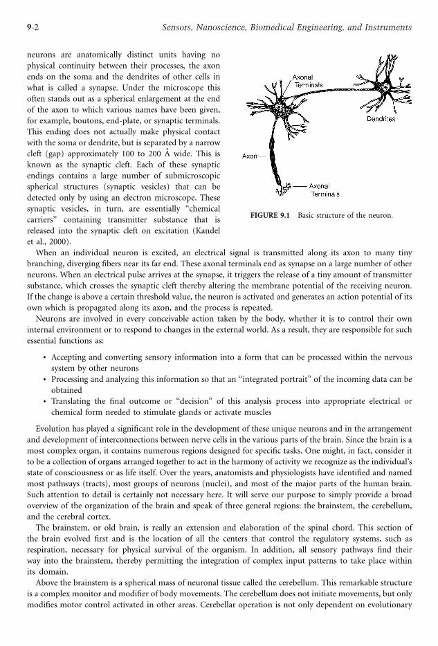
neurons are anatomically distinct units having no
physical continuity between their processes, the axon
ends on the soma and the dendrites of other cells in
what is called a synapse. Under the microscope this
often stands out as a spherical enlargement at the end
of the axon to which various names have been given,
for example, boutons, end-plate, or synaptic terminals.
This ending does not actually make physical contact
with the soma or dendrite, but is separated by a narrow
cleft (gap) approximately 100 to 200 A wide. This is
known as the synaptic cleft. Each of these synaptic
endings contains a large number of submicroscopic
spherical structures (synaptic vesicles) that can be
detected only by using an electron microscope. These
synaptic vesicles, in turn, are essentially ‘‘chemical
carriers’’ containing transmitter substance that is
released into the synaptic cleft on excitation (Kandel
et al., 2000).
When an individual neuron is excited, an electrical signal is transmitted along its axon to many tiny
branching, diverging fibers near its far end. These axonal terminals end as synapse on a large number of other
neurons. When an electrical pulse arrives at the synapse, it triggers the release of a tiny amount of transmitter
substance, which crosses the synaptic cleft thereby altering the membrane potential of the receiving neuron.
If the change is above a certain threshold value, the neuron is activated and generates an action potential of its
own which is propagated along its axon, and the process is repeated.
Neurons are involved in every conceivable action taken by the body, whether it is to control their own
internal environment or to respond to changes in the external world. As a result, they are responsible for such
essential functions as:
. Accepting and converting sensory information into a form that can be processed within the nervous
system by other neurons. Processing and analyzing this information so that an ‘‘integrated portrait’’ of the incoming data can be
obtained. Translating the final outcome or ‘‘decision’’ of this analysis process into appropriate electrical or
chemical form needed to stimulate glands or activate muscles
Evolution has played a significant role in the development of these unique neurons and in the arrangement
and development of interconnections between nerve cells in the various parts of the brain. Since the brain is a
most complex organ, it contains numerous regions designed for specific tasks. One might, in fact, consider it
to be a collection of organs arranged together to act in the harmony of activity we recognize as the individual’s
state of consciousness or as life itself. Over the years, anatomists and physiologists have identified and named
most pathways (tracts), most groups of neurons (nuclei), and most of the major parts of the human brain.
Such attention to detail is certainly not necessary here. It will serve our purpose to simply provide a broad
overview of the organization of the brain and speak of three general regions: the brainstem, the cerebellum,
and the cerebral cortex.
The brainstem, or old brain, is really an extension and elaboration of the spinal chord. This section of
the brain evolved first and is the location of all the centers that control the regulatory systems, such as
respiration, necessary for physical survival of the organism. In addition, all sensory pathways find their
way into the brainstem, thereby permitting the integration of complex input patterns to take place within
its domain.
Above the brainstem is a spherical mass of neuronal tissue called the cerebellum. This remarkable structure
is a complex monitor and modifier of body movements. The cerebellum does not initiate movements, but only
modifies motor control activated in other areas. Cerebellar operation is not only dependent on evolutionary
FIGURE 9.1 Basic structure of the neuron.
9-2 Sensors, Nanoscience, Biomedical Engineering, and Instruments

development, but relies heavily on actual use and patterns of learned motor behavior acquired throughout life.
It is for this reason that the movements of a gymnast are smooth and seemingly effortless.
The most conspicuous part of all in the human brain is the cerebral cortex. Compared to most mammals, it
is so large in man that it becomes a covering that surrounds and hides most of the other regions of the brain.
Wrinkled and folded, the cerebral tissue is literally pressed into the limited space allocated to it. Although it
has been possible to ascertain that certain cortical areas such as the visual cortex, the sensory projection area,
and the motor strip are associated with specific functions, the overall operation of this complex structure is
still not completely understood. However, for the sake of convenience, it has been arbitrarily divided (based
primarily on anatomical considerations) into the following areas: frontal lobe, parietal lobe, temporal lobe,
and occipital lobe (Figure 9.2). Each of these segments of the cortex, which is the source of intellectual and
imaginative capacities, includes millions of neurons and a host of interconnections.
It is generally agreed that brain function is based on the organization of the activity of large numbers of
neurons into coherent patterns. Since the primary mode of activity of these nerve cells is electrical in nature, it
is not surprising that a composite of this activity can be detected in the form of electrical signals. Of extreme
interest, then, are the actual oscillations, rhythms, and patterns seen in the cryptic flow of electrical energy
coming from the brain itself, i.e., in the EEG.
Historical Perspective
In 1875, Caton published the initial account of the recording of the spontaneous electrical activity of the brain
from the cerebral cortex of an experimental animal. The amplitude of these electrical oscillations was so low,
that is, on the order of microvolts, that Caton’s discovery is all the more amazing because it was made 50 years
before suitable electronic amplifiers became available. In 1924, Hans Berger, of the University of Jena in
Austria, carried out the first human EEG recordings using electrical metal strips pasted to the scalps of his
subjects as electrodes and a sensitive galvanometer as the recording instrument. Berger was able to measure the
irregular, relatively small electrical potentials (i.e., 50 to 100 mV) coming from the brain. By studying the
successive positions of the moving element of the galvanometer recorded on a continuous roll of paper, he was
able to observe the resultant patterns in these brain waves as they varied with time. From 1924 to 1938, Berger
laid the foundation for many of the present applications of electroencephalography. He was the first to use the
word electroencephalogram in describing these brain potentials in man. Berger noted that these brain waves
were not entirely random, but instead displayed certain periodicities and regularities. For example, he
observed that although these brain waves were slow (i.e., exhibited a synchronized patter of high amplitude
and low frequency, ,3 Hz) in sleep and states of depressed function, they were faster (i.e., exhibited a
desynchronized pattern of low amplitude and high frequency, 15 to 25 Hz) during waking behavior. He
suggested, quite correctly, that the brain’s activity changed in a consistent and recognizable fashion when the
general status of the subject changed, as from relaxation to alertness. Berger also concluded that these brain
waves could be greatly affected by certain pathological conditions after noting the marked increase in the
FIGURE 9.2 Major divisions of the cerebral cortex.
9-3Bioelectronics and Instruments
amplitude of these brain waves brought about by convulsive seizures. However, despite the insights provided
by these studies, Berger’s original paper published in 1929 did not invite much attention. In essence, the efforts
of this most remarkable pioneer were largely ignored until similar investigations were carried out and verified
by British investigators.
It was not until 1934 when Adrian and Matthews published their classic paper verifying Berger’s findings
that the reality of human brain waves was accepted and EEG studies were put on a firmly established basis.
One of their primary contributions was the identification of certain rhythms in the EEG, regular oscillations
at approximately 10 to 12 Hz in the occipital lobes of the cerebral cortex. They found that this alpha rhythm
in the EEG would disappear when the brain displayed any type of attention or alertness or focused on
objects in the visual field. The physiological basis for these results, the ‘‘arousing influence’’ of external
stimuli on the cortex, was not formulated until 1949 when Moruzzi and Magoun demonstrated the existence
of widely spread pathways through the central reticular core of the brainstem capable of exerting a diffuse
activating influence on the cerebral cortex. This reticular activating system has been called the brain’s
response selector because it alerts the cortex to focus on certain incoming information while ignoring other.
It is for this reason that a sleeping mother will immediately be awakened by her crying baby or the smell of
smoke, and yet ignores the traffic outside her window or the television still playing in the next room. An
in-depth discussion of these early studies is beyond the scope of this presentation; however, for the interested
reader an excellent historical review of this early era in brain research has been recorded in a fascinating text
by Brazier (1968).
EEG Recording Techniques
Scalp recordings of spontaneous neuronal activity in the brain, identified as the EEG, allow measurement of
potential changes over time between a signal electrode and a reference electrode (Kondraski, 1986). Compared
to other biopotentials, such as the electrocardiogram, the EEG is extremely difficult for an untrained observer
to interpret. As might be expected, partially as a result of the spatial mapping of functions onto different
regions of the brain, correspondingly different waveforms are visible, depending on electrode placement.
Recognizing that some standardization was necessary for comparison of research as well as clinical EEG
records, the International Federation in Electroencephalography and Clinical Neurophysiology adopted the
10 to 20 electrode placement system (Jasper, 1958). Additional electrodes to monitor extracerebral con-
taminants of the EEG such as eye movement, EKG, and muscle activity are essential. The acquisition of EEG
for quantitative analysis should also require the ability to view the EEG during collection on a polygraph or
high-resolution video display.
Since amplification, filtering, and digitization determine the frequency characteristics of the EEG and the
source of potential artifacts, the acquisition parameters must be chosen with an understanding of their effects
on signal acquisition and subsequent analysis. Amplification, for example, increases the amplitude range
(volts) of the analog-to-digital converter (ADC). The resolution of the ADC is determined by the smallest
amplitude of steps that can be sampled. This is calculated by dividing the voltage range of the ADC by 2 to the
power of the number of bits of the ADC. For example, an ADC with a range of ^5 V with 12-bit resolution
can resolve samples as small as ^2.4 mV. Appropriate matching of amplification and ADC sensitivity permits
resolution of the smallest signal while preventing clipping of the largest signal amplitudes.
The bandwidth of the filters and the rate of digitization determine the frequency components of interest
that are passed, while other frequencies outside the band of interest that may represent potential artifacts, such
as aliasing, are rejected. A filter’s characteristics are determined by the rate of the amplitude decrease at the
bandwidth’s upper and lower edges. Proper digital representation of the analog signal depends on the rate of
data sampling, which is governed by the Nyquist theorem that states that data sampling should be at least
twice the highest frequency of interest.
In addition to the information available from spontaneous electrical activity of the EEG, the brain’s
electrical response to sensory stimulation can contribute data as to the status of cortical and subcortical
regions activated by sensory input. Because of the relatively small amplitude of a stimulus-evoked potential as
compared to the spontaneous EEG potentials, the technique of signal averaging is used to enhance the
9-4 Sensors, Nanoscience, Biomedical Engineering, and Instruments

stimulus-evoked response. Stimulus averaging takes advantage of the fact that the brain’s electrical response is
time-locked to the onset of the stimulus and the nonevoked background potentials are randomly distributed
in time. Consequently, the average of multiple stimulus responses will result in the enhancement of time-
locked activity, while the averaged random background activity will approach zero. The result is an evoked
response that consists of a number of discrete and replicable peaks that occur, depending upon the stimulus
and the recording parameters, at predicted latencies from the onset of stimulation. The spatial localization of
maximum peak amplitudes has been associated with cortical generators in primary sensory cortex.
Instrumentation required for EEG recordings can be simple or elaborate (Kondraski, 1986). (Note:
Although the discussion presented in this section is for a single-channel system it can be extended to
simultaneous multichannel recordings simply by multiplying the hardware by the number of channels
required. In cases that do not require true simultaneous recordings, special electrode selector panels can
minimize hardware requirements.) Any EEG system consists of electrodes, amplifiers (with appropriate filters)
and a recording device.
Commonly used scalp electrodes consist of Ag-AgCl disks, 1 to 3 mm in diameter, with a very flexible long
lead that can be plugged into an amplifier. Although it is desirable to obtain a low-impedance contact at the
electrode–skin interface (less than 10 kO), this objective is confounded by hair and the difficulty of
mechanically stabilizing the electrodes. Conductive electrode paste helps obtain low impedance and keep the
electrodes in place. A type of cement (collodion) is used to fix small patches of gauze over electrodes for
mechanical stability, and leads are usually taped to the subject to provide some strain relief. Slight abrasion of
the skin is sometimes used to obtain better electrode impedances, but this can cause irritation and sometimes
infection (as well as pain in sensitive subjects).
For long-term recordings, as in seizure monitoring, electrodes present major problems. Needle electrodes,
which must be inserted into the tissue between the surface of the scalp and skull, are sometimes useful.
However, the danger of infection increases significantly. Electrodes with self-contained miniature amplifiers
are somewhat more tolerant because they provide a low-impedance source to interconnecting leads, but they
are expensive. Despite numerous attempts to simplify the electrode application process and to guarantee long-
term stability, none has been widely accepted.
Instruments are available for measuring impedance between electrode pairs. The procedure is
recommended strongly as good practice, since high impedance leads to distortions that may be difficult to
separate from actual EEG signals. In fact, electrode impedance monitors are built into some commercial
devices for recording EEGs. Standard dc ohmmeters should not be used, since they apply a polarizing current
that causes build-up of noisy electrode potential at the skin–electrode interface. Commercial devices apply a
known-amplitude sinusoidal voltage (typically 1 kHz) to an electrode pair circuit and measure root mean
square (rms) current, which is directly related to the magnitude of the impedance.
From carefully applied electrodes, signal amplitudes of 1 to 10 mV can be obtained. Considerable
amplification (gain ¼ 106) is required to bring these levels up to an acceptable level for input to recording
devices. Because of long electrode leads and the common electrically noisy environment where recordings take
place, differential amplifiers with inherently high input impedance and high common mode rejection ratios
are essential for high-quality EEG recordings.
In some facilities, special electrically shielded rooms minimize environmental electrical noise, particularly
60-Hz alternating current (ac) line noise. Since much of the information of interest in the EEG lies in the
frequency bands less than 40 Hz, low-pass filters in the amplifier can be switched into attenuate 60-Hz noise
sharply.
For attenuating ac noise when the low-pass cutoff is greater than 60 Hz, many EEG amplifiers have notch
filters that attenuate only frequencies in a narrow band centered around 60 Hz. Since important signal
information may also be attenuated, notch filtering should be used as a last resort; one should try to identify
and eliminate the source of interference instead.
In trying to identify 60-Hz sources to eliminate or minimize their effect, it is sometimes useful to use a
dummy source, such as a fixed 100-kO resistor attached to the electrodes. An amplifier output represents only
contributions from interfering sources. If noise can be reduced to an acceptable level (at least by a factor of ten
less than EEG signals) under this condition, one is likely to obtain uncontaminated EEG records.
9-5Bioelectronics and Instruments
Different types of recording instruments obtain a temporary or permanent record of the EEG. The most
common recording device is a pen or chart recorder (usually multichannel) that is an integral part of most
commercially available EEG instruments. The bandwidth of clinical EEGs is relatively low (less than 40 Hz)
and therefore within the frequency response capabilities of these devices. Recordings are on a long sheet of
continuous paper (from a folded stack), fed past the moving pen at one of several selectable constant speeds.
The paper speed translates into distance per unit time or cycles per unit time, to allow EEG interpreters to
identify different frequency components or patterns within the EEG. Paper speed is selected according to the
monitoring situation at hand: slow speeds (10 mm/sec) for observing the spiking characteristically associated
with seizures and faster speeds (up to 120 mm/sec) for the presence of individual frequency bands in the EEG.
In addition to (or instead of) a pen recorder, the EEG may be recorded on a multichannel frequency
modulated (FM) analog tape recorder. During such recordings, a visual output device such as an oscilloscope
or video display is necessary to allow visual monitoring of signals, so that corrective action (reapplying the
electrodes and so on) can take place immediately if necessary.
Sophisticated FM cassette recording and playback systems allow clinicians to review long EEG recordings
over a greatly reduced time, compared to that required to flip through stacks of paper or observe recordings as
they occur in real time. Such systems take advantage of time compensation schemes, whereby a signal recorded
at one speed (speed of the tape moving past the recording head of the cassette drive) is played back at a
different, faster speed. The ratio of playback to recording speed is known, so the appropriate correction factor
can be applied to played-back data to generate a properly scaled video display. A standard ratio of 60:1 is often
used. Thus, a trained clinician can review each minute of real-time EEG in 1 sec. The display appears to be
scrolled at a high rate horizontally across the display screen. Features of these instruments allow the clinician
to freeze a segment of EEG on the display and to slow down or accelerate tape speed from the standard
playback as needed. A time mark channel is usually displayed as one of the traces as a convenient reference
(vertical ‘‘tick’’ mark displayed at periodic intervals across the screen).
Computers can also be recording devices, digitizing (converting to digital form) one or several amplified
EEG channels at a fixed rate. In such sampled data systems, each channel is repeatedly sampled at a fixed
time interval (sample interval), and this sample is converted into a binary number representation by an ADC.
The ADC is interfaced to a computer system so that each sample can be saved in the computer’s memory. A set
of such samples, acquired at a sufficient sampling rate (at least two times the highest frequency component
in the sampled signal), is sufficient to represent all the information in the waveform. To ensure that the signal
is band-limited, a low-pass filter with a cutoff frequency equal to the highest frequency of interest is used.
Since physically realizable filters do not have the ideal characteristics, the sampling rate is usually greater than
two times the filter’s cutoff frequency. Furthermore, once converted to a digital format, digital filtering
techniques can be used.
On-line computer recordings are only practical for short-term recordings, or for situations in which the
EEG is immediately processed. This limitation is primarily due to storage requirements. For example, a typical
sampling rate of 128 Hz yields 128 new samples per second that require storage. For an eight-channel
recording, 1024 samples are acquired per second. A 10-minute recording period yields 614,400 data points.
Assuming 8-bit resolution per sample, over 0.5 megabyte (MB) of storage is required to save the 10-minute
recording.
Processing can consist of compression for more efficient storage (with associated loss of total information
content), as in data record or epoch averaging associated with evoked responses, or feature extraction and
subsequent pattern recognition, as in automated spike detection in seizure monitoring.
Frequency Analysis of the EEG
In general, the EEG contains information regarding changes in the electrical potential of the brain obtained
from a given set of recording electrodes. These data include the characteristic waveform with its variation in
amplitude, frequency, phase, etc. and the occurrence of brief electrical patterns, such as spindles. Any analysis
procedure cannot simultaneously provide information regarding all of these variables. Consequently, the
selection of any analytic technique will emphasize changes in one particular variable at the expense of the
9-6 Sensors, Nanoscience, Biomedical Engineering, and Instruments
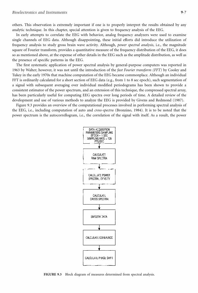
others. This observation is extremely important if one is to properly interpret the results obtained by any
analytic technique. In this chapter, special attention is given to frequency analysis of the EEG.
In early attempts to correlate the EEG with behavior, analog frequency analyzers were used to examine
single channels of EEG data. Although disappointing, these initial efforts did introduce the utilization of
frequency analysis to study gross brain wave activity. Although, power spectral analysis, i.e., the magnitude
square of Fourier transform, provides a quantitative measure of the frequency distribution of the EEG, it does
so as mentioned above, at the expense of other details in the EEG such as the amplitude distribution, as well as
the presence of specific patterns in the EEG.
The first systematic application of power spectral analysis by general-purpose computers was reported in
1963 by Walter; however, it was not until the introduction of the fast Fourier transform (FFT) by Cooley and
Tukey in the early 1970s that machine computation of the EEG became commonplace. Although an individual
FFT is ordinarily calculated for a short section of EEG data (e.g., from 1 to 8 sec epoch), such segmentation of
a signal with subsequent averaging over individual modified periodograms has been shown to provide a
consistent estimator of the power spectrum, and an extension of this technique, the compressed spectral array,
has been particularly useful for computing EEG spectra over long periods of time. A detailed review of the
development and use of various methods to analyze the EEG is provided by Givens and Redmond (1987).
Figure 9.3 provides an overview of the computational processes involved in performing spectral analysis of
the EEG, i.e., including computation of auto and cross-spectra (Bronzino, 1984). It is to be noted that the
power spectrum is the autocorrellogram, i.e., the correlation of the signal with itself. As a result, the power
FIGURE 9.3 Block diagram of measures determined from spectral analysis.
9-7Bioelectronics and Instruments
spectrum provides only magnitude information in the frequency domain; it does not provide any data
regarding phase. The power spectrum is computed by:
Pðf Þ ¼ Re2½Xðf Þ þ Im2½Xðf Þ ð9:1Þ
where X(f) is the Fourier transform of the EEG.
Power spectral analysis not only provides a summary of the EEG in a convenient graphic form, but also
facilitates statistical analysis of EEG changes, which may not be evident on simple inspection of the records. In
addition to absolute power derived directly from the power spectrum, other measures calculated from absolute
power have been demonstrated to be of value in quantifying various aspects of the EEG. Relative power
expresses the percent contribution of each frequency band to the total power and is calculated by dividing the
power within a band by the total power across all bands. Relative power has the benefit of reducing the
intersubject variance associated with absolute power that arises from intersubject differences in skull and scalp
conductance. The disadvantage of relative power is that an increase in one frequency band will be reflected in
the calculation by a decrease in other bands; for example, it has been reported that directional shifts between
high and low frequencies are associated with changes in cerebral blood flow and metabolism. Power ratios
between low (0 to 7 Hz) and high (10 to 20 Hz) frequency bands have been demonstrated to be an accurate
estimator of changes in cerebral activity during these metabolic changes.
Although the power spectrum quantifies activity at each electrode, other variables derivable from FFToffer a
measure of the relationship between activity recorded at distinct electrode sites. Coherence (which is a
complex number), calculated from the cross-spectrum analysis of two signals, is similar to cross-correlation in
the time domain. The magnitude squared coherence (MSC) values range from 1 to 0, indicating maximum or
no synchrony, respectively, and are independent of power. The temporal relationship between two signals is
expressed by phase, which is a measure of the lag between two signals for common frequency components or
bands. Phase is expressed in units of degrees, 0– indicating no time lag between signals and 180– if the
signals are of opposite polarity. Phase can also be transformed into the time domain, giving a measure of the
time difference between two frequencies.
Cross-spectrum is computed by:
cross-spectrum ¼ Xðf ÞY * ðf Þ ð9:2Þ
where X(f), Y(f) are Fourier transforms and * indicates complex conjugates and coherence is calculated by
coherence ¼ cross-spectrumffiffiffiffiffiffiffiffiffiffiffiffiffiffiffiffiffiffiPXðf Þ PYðf Þp ð9:3Þ
Since coherence is a complex number, the phase is simply the angle associated with the polar expression of
that number. MSC and phase represent measures that can be employed to investigate the cortical interactions
of cerebral activity. For example, short (intracortical) and long (cortico-cortical) pathways have been proposed
as the anatomic substrate underlying the spatial frequency and patterns of coherence. Therefore, discrete
cortical regions linked by such fiber systems should demonstrate a relatively high degree of synchrony, whereas
the time lag between signals, as represented by phase, quantifies the extent to which one signal leads another.
Nonlinear Analysis of the EEG
As mentioned earlier, the EEG has been studied extensively using signal-processing schemes, most of which are
based on the assumption that the EEG is a linear, Gaussian process. Although linear analysis schemes are
computationally efficient and useful, they only utilize information retained in the autocorrelation function
(i.e., the second-order cumulant). Additional information stored in higher-order cumulants is therefore
ignored by linear analysis of the EEG. Thus, while the power spectrum provides the energy distribution of a
9-8 Sensors, Nanoscience, Biomedical Engineering, and Instruments
stationary process in the frequency domain, it cannot distinguish nonlinearly coupled frequencies from
spontaneously generated signals with the same resonance condition (Nikias and Raghvveer, 1987).
There is evidence showing that the amplitude distribution of the EEG often deviates from Gaussian
behavior. It has been reported, for example, that the EEGs of humans involved in the performance of mental
arithmetic tasks exhibit significant non-Gaussian behavior. In addition, the degree of deviation from Gaussian
behavior of the EEG has been shown to depend to the behavioral state, with the state of slow-wave sleep
showing less Gaussian behavior than quiet waking, which is less Gaussian than rapid eye movement (REM)
sleep (Ning and Bronzino, 1989; Ferri et al., 2002, 2003). Nonlinear signal-processing algorithms such as
bispectral analysis are therefore necessary to address non-Gaussian and nonlinear behavior of the EEG in order
to better describe it in the frequency domain.
What exactly is the bispectrum? For a zero-mean, stationary process X(k), the bispectrum, by definition, is
the Fourier transform of its third-order cumulant (TOC) sequence:
Bðo1;o2Þ ¼Xa
m¼ a
Xan¼ a
Cðm; nÞe jðw1mþw2nÞ ð9:4Þ
The TOC sequence C(m, n) is defined as the expected value of the triple product:
Cðm; nÞ ¼ EfXðkÞXðkþmÞXðkþ nÞg ð9:5Þ
If process X(k) is purely Gaussian, then its third-order cumulant C(m, n) is zero for each (m, n), and
consequently, its Fourier transform, the bispectrum, B(o1, o2) is also zero. This property makes the estimated
bispectrum an immediate measure describing the degree of deviation from Gaussian behavior. In our studies
(Ning and Bronzino, 1989), the sum of magnitude of the estimated bispectrum was used as a measure to
describe the EEG’s deviation from Gaussian behavior, that is:
D ¼X
ðo1;o2ÞjBðo1;o2Þj
Using bispectral analysis, the existence of significant quadratic phase coupling (QPC) in the hippocampal EEG
obtained during REM sleep in the adult rat was demonstrated (Ning and Bronzino, 1989, 1990). The result
of this nonlinear coupling is the appearance, in the frequency spectrum, of a small peak centered at
approximately 13 to 14 Hz (beta range) that reflects the summation of the two theta frequency (i.e., in the
6- to 7-Hz range) waves. Conventional power spectral (linear) approaches are incapable of distinguishing the
fact that this peak results from the interaction of these two generators and is not intrinsic to either.
To examine the phase relationship between nonlinear signals collected at different sites, the cross-
bispectrum is also a useful tool. For example, given three zero-mean, stationary processes xj(n)j ¼ 1, 2, 3,
there are two conventional methods for determining the cross-bispectral relationship, direct and indirect. Both
methods first divide these three processes into M segments of shorter but equal length. The direct method
computes the Fourier transform of each segment for all three processes and then estimates the cross-
bispectrum by taking the average of triple products of Fourier coefficients over M segments, that is:
Bx1x2x3ðo1;o2Þ ¼ 1
M
XMm¼ 1
Xm1 ðo1ÞXm
2 ðo2ÞXm*3 ðo1 þ o2Þ ð9:7Þ
where Xjm(o) is the Fourier transform of the mth segment of xj(n), and * indicates the complex conjugate.
9-9Bioelectronics and Instruments
The indirect method computes the third-order cross-cumulant sequence for all segments:
Cmx1x2x3ðk; lÞ ¼
Xn2t
xm1 ðnÞxm2 ðnþ kÞxm3 ðnþ lÞ ð9:8Þ
where t is the admissible set for argument n. The cross-cumulant sequences of all segments will be averaged togive a resultant estimate:
Cx1x2x3ðk; lÞ ¼1
M
XMm¼ 1
Cmx1x2x3ðk; lÞ ð9:9Þ
The cross-bispectrum is then estimated by taking the Fourier transform of the third-order cross-cumulant
sequence:
Bx1x2x3ðo1;o2Þ ¼Xak¼ a
Xal¼ a
Cx1x2x3ðk; l Þ jðo1kþo2lÞ ð9:10Þ
Since the variance of the estimated cross-bispectrum is inversely proportional to the length of each segment,
computation of the cross-bispectrum for processes of finite data length requires careful consideration of both
the length of individual segments and the total number of segments to be used.
The cross-bispectrum can be applied to determine the level of cross-QPC occurring between x1(n) and
x2(n) and its effects on x3(n). For example, a peak at Bx1x2x3(o1, o2) suggests that the energy component
at frequency o1 þ o2 of x3(n) is generated due to the QPC between frequency o1 of x1(n) and frequency
o2 of x2(n). In theory, the absence of QPC will generate a flat cross-bispectrum. However, due to the finite
data length encountered in practice, peaks may appear in the cross-bispectrum at locations where there is no
significant cross-QPC. To avoid improper interpretation, the cross-bicoherence index, which indicates the
significance level of cross-QPC, can be computed as follows:
bicx1x2x3ðo1;o2Þ ¼Bx1x2x3ðo1;o2Þffiffiffiffiffiffiffiffiffiffiffiffiffiffiffiffiffiffiffiffiffiffiffiffiffiffiffiffiffiffiffiffiffiffi
Px1ðo1ÞPx2ðo2ÞPx3ðo1 þ o2Þp ð9:11Þ
where Pxj(o) is the power spectrum of process xj(n). The theoretical value of the bicoherence index ranges
between 0 and 1, i.e., from nonsignificant to highly significant.
In situations where the interest is the presence of QPC and its effects on x(n), the cross-bispectrum
equations can be modified by replacing x1(n) and x3(n) with x(n) and x2(n) with y(n), that is:
Bxyzðo1;o2Þ ¼ 1
M
XMm¼ 1
Xmðo1ÞYmðo2ÞXm*ðo1 þ o2Þ ð9:12Þ
In theory, both methods will lead to the same cross-bispectrum when data length is infinite. However, with
finite data records, direct and indirect methods generally lead to cross-bispectrum estimates with different
shapes (Figure 9.4). Therefore, like power spectrum estimation, users have to choose an appropriate method
to extract the information desired.
Topographic Mapping
Computerized tomography (CT) and magnetic resonance imaging (MRI) have demonstrated the impact of
spatial displays on data interpretation and analysis. Similarly, mapping techniques have been applied to
electrophysiologic data to depict the spatial information available from multi-electrode recordings. This effort
has been assisted by the development and implementation of low-cost, high-resolution graphic displays on
9-10 Sensors, Nanoscience, Biomedical Engineering, and Instruments
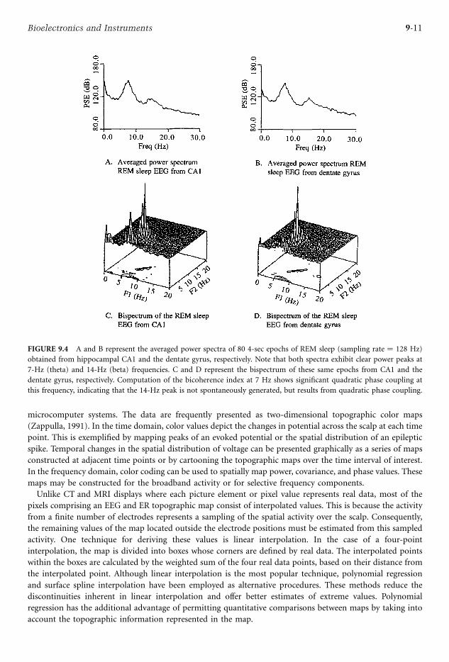
microcomputer systems. The data are frequently presented as two-dimensional topographic color maps
(Zappulla, 1991). In the time domain, color values depict the changes in potential across the scalp at each time
point. This is exemplified by mapping peaks of an evoked potential or the spatial distribution of an epileptic
spike. Temporal changes in the spatial distribution of voltage can be presented graphically as a series of maps
constructed at adjacent time points or by cartooning the topographic maps over the time interval of interest.
In the frequency domain, color coding can be used to spatially map power, covariance, and phase values. These
maps may be constructed for the broadband activity or for selective frequency components.
Unlike CT and MRI displays where each picture element or pixel value represents real data, most of the
pixels comprising an EEG and ER topographic map consist of interpolated values. This is because the activity
from a finite number of electrodes represents a sampling of the spatial activity over the scalp. Consequently,
the remaining values of the map located outside the electrode positions must be estimated from this sampled
activity. One technique for deriving these values is linear interpolation. In the case of a four-point
interpolation, the map is divided into boxes whose corners are defined by real data. The interpolated points
within the boxes are calculated by the weighted sum of the four real data points, based on their distance from
the interpolated point. Although linear interpolation is the most popular technique, polynomial regression
and surface spline interpolation have been employed as alternative procedures. These methods reduce the
discontinuities inherent in linear interpolation and offer better estimates of extreme values. Polynomial
regression has the additional advantage of permitting quantitative comparisons between maps by taking into
account the topographic information represented in the map.
FIGURE 9.4 A and B represent the averaged power spectra of 80 4-sec epochs of REM sleep (sampling rate ¼ 128 Hz)
obtained from hippocampal CA1 and the dentate gyrus, respectively. Note that both spectra exhibit clear power peaks at
7-Hz (theta) and 14-Hz (beta) frequencies. C and D represent the bispectrum of these same epochs from CA1 and the
dentate gyrus, respectively. Computation of the bicoherence index at 7 Hz shows significant quadratic phase coupling at
this frequency, indicating that the 14-Hz peak is not spontaneously generated, but results from quadratic phase coupling.
9-11Bioelectronics and Instruments
Maps can be presented in any of several projections to assist in interpretation (Zappulla, 1991). The most
common projection is the top view which presents the spatial distribution of variables from all leads
simultaneously. Lateral, posterior, and anterior projections highlight focal areas of interest. Although mapping
presents a method by which spatial information can be efficiently communicated, it is important to be alert to
the artifacts that can arise from map construction and manipulation. Topographic spatial artifacts that can
lead to misinterpretation include ring enhancement around a spike using source-derivation references, spatial
aliasing arising from linear interpolation which causes maximal activity to be mapped at electrode sites, the
enhancement of activity away from the midline, and the attenuation of midline activity on amplitude
asymmetry maps (centrifugal effect).
The quality of the spatial information derivable from EEG recordings depends upon the number of
recording electrodes, the choice of the reference electrode, and the conductive properties of intracranial and
extracranial structures. The localization of cortical activity from scalp recordings assumes that the potentials
recorded from the scalp reflect cortical activity generated in proximity to the recording electrode. Therefore,
the greater the density of recording electrodes, the more accurate the estimate of the spatial distribution of scalp
potentials and the localization of cortical generators. However, since the distance between the cortical source
and recording electrode, as well as the low conductivity of the skull, results in a selective attenuation of small
dipole fields, most available EEG information can be obtained with an average scalp–electrode spacing of 2 cm.
Topographic maps are constructed frommonopolar electrodes referenced to a common cephalic (linked ears
or mandible, chin and nose) or noncephalic (linked clavicles or a balanced sternum-vertebra) electrode.
Although the reference electrode should be free of any EEG activity, in practice most cephalic electrodes contain
some EEG activity, while noncephalic electrodes are a potential source of EKG or muscle activity. Differential
amplification of an EEG-contaminated reference electrode can decrease or cancel similar activity in neighboring
electrodes, while at electrodes distant from the reference, the injected activity will be present as a potential of
opposite polarity. Similarly, noncerebral potentials can be injected into scalp electrodes and misinterpreted as
cerebral activity. Therefore, a nonneutral reference electrode can result in misleading map configurations.
Several techniques have been applied to circumvent this problem. The construction of multiple maps using
several different references can sometimes assist in differentiating active and reference electrode activity. This can
be accomplished by acquiring serial EEG records using different references. Alternatively, various references can
be acquired simultaneously during acquisition, and various montages can be digitally reconstructed, post hoc.
A more computationally intensive method for localizing a source at an electrode involves calculating the
local source activity at any one electrode based on the average activity of its neighbors, weighted by their
distance from the source. The technique has the advantage of suppressing potentials that originate outside the
measurement area and weighing factors for implementing source deviation techniques for each of the
electrodes in the 10 to 20 system are available.
Another reference technique, the average head reference, uses the average activity of all active electrodes as
the common reference. In this approach, the activity at any one electrode will vary depending upon the
activity at the site of the reference electrode, which can be anywhere on the recording montage. Therefore, for
N number of recording electrodes, each being a potential reference, there are N – 1 possible voltage
measurements at each instant of time for each electrode. Maps constructed using the average head reference
represent a unique solution to the problem of active reference electrodes in that the average reference produces
an amplitude-weighted reference-free map of maximal and minimal field potentials. Power maps constructed
from the average reference best depict the spatial orientation of the generating field, and the areas with
extreme values are closest to the generating processes (Zappulla, 1991).
Topographical maps represent an efficient format for displaying the extensive amount of data generated by
quantitative analysis. However, for reasons discussed above, the researcher and clinician must be cautious in
deriving spatial and functional conclusions frommapped data. Although the replicability of map configurations
across subjects or experimental conditions may represent a useful basis for experimental and diagnostic
classification, judgments concerning the localization of cortical generators or functional localization of cerebral
activity are less certain and more controversial. Research continues on defining models and validating
assumptions that relate scalp potentials to cortical generators in an attempt to arrive at accurate mathematical
solutions that can be applied to mapping functions.
9-12 Sensors, Nanoscience, Biomedical Engineering, and Instruments
Defining Terms
Bispectra: Computation of the frequency distribution of the EEG exhibiting nonlinear behavior.
Cross spectra: Computation of the energy in the frequency distribution of two different electrical signals.
Electroencephalogram (EEG): Recordings of the electrical potentials produced by the brain.
Fast Fourier transform (FFT): Algorithms that permit rapid computation of the Fourier transform of an
electrical signal, thereby representing it in the frequency domain.
Magnitude squared coherence (MSC): A measure of the degree of synchrony between two electrical
signals at specific frequencies.
Power spectral analysis: Computation of the energy in the frequency distribution of an electrical signal.
Quadratic phase coupling: A measure of the degree to which specific frequencies interact to produce a
third frequency.
References
M. Brazier, Electrical Activity of the Nervous System, 3rd ed., Baltimore, MD: Williams and Wilkins, 1968.
J.D. Bronzino, M. Kelly, and C. Cordova, ‘‘Utilization of amplitude histograms to quantify the EEG: effects of
systemic administration of morphine in the chronically implanted rat,’’ IEEE Trans. Biomed. Eng.,
vol. 28, no. 10, p. 673, 1981.
J.D. Bronzino, ‘‘Quantitative analysis of the EEG: general concepts and animal studies,’’ IEEE Trans. Biomed.
Eng., vol. 31, no. 12, p. 850, 1984.
J.W. Cooley and J.S. Tukey, ‘‘An algorithm for the machine calculation of complex Fourier series,’’
Math. Comput., vol. 19, p. 267, 1965.
R. Ferri, L. Parrino, A. Smerieri, M.G. Terzano, M. Elia, S.A. Musumeci, S. Pettinato, and C.J. Stam, ‘‘Non-
linear EEG measures during sleep: effects of the different sleep stages and cyclic alternating pattern,’’
Int. J. Psychophysiol., vol. 43, no. 3, pp. 273–286, 2002.
R. Ferri, R. Chiaramonti, M. Elia, S.A. Musumeci, A. Ragazzoni, and C.J. Stam, ‘‘Nonlinear EEG analysis in
premature and full-term newborns,’’ Clin. Neurophysiol., vol. 114, no. 7, pp. 1176–1180, 2003.
A.S. Givens and A. Remond, Eds., ‘‘Methods of analysis of brain electrical and magnetic signals,’’ in EEG
Handbook, vol. 1, Amsterdam: Elsevier, 1987.
S.M. Kay and S.L. Maple, ‘‘Spectrum analysis—a modern perspective,’’ Proc. IEEE., vol. 69, p. 1380, 1981.
E.R. Kandel, J.H. Schwartz, and T.M. Jessel, Principles of Neural Science, 4th ed., New York: McGraw-Hill,
2000.
G.V. Kondraski, ‘‘Neurophysiological measurements,’’ in Biomedical Engineering and Instrumentation,
J.D. Bronzino, Ed., Boston, MA: PWS Publishing, pp. 138–179, 1986.
C.L. Nikias and M.R. Raghuveer, ‘‘Bispectrum estimation: a digital signal processing framework,’’ Proc. IEEE,
vol. 75, p. 869, 1987.
T. Ning and J.D. Bronzino, ‘‘Bispectral analysis of the rat EEG during different vigilance states,’’ IEEE Trans.
Biomed. Eng., vol. 36, no. 4, p. 497, 1989
T. Ning and J.D. Bronzino, ‘‘Autoregressive and bispectral analysis techniques: EEG applications, Special Issue
on Biomedical Signal Processing,’’ IEEE Eng. Med. Biol. Mag., vol. 9, p. 47, 1990.
J.R. Smith, ‘‘Automated analysis of sleep EEG data,’’ in Clinical Applications of Computer Analysis of EEG and
Other Neurophysiological Signals, EEG Handbook, revised series, vol. 2, Amsterdam: Elsevier, 1986,
pp. 93–130.
Further Information
The Biomedical Engineering Handbook, J.D. Bronzino, Ed., Boca Raton, FL: CRC Press, 1st ed. 1995,
2nd ed. 2000.
See also the journals, Annals of Biomedical Engineering: IEEE Transactions in Biomedical Engineering and
Electroencephalography and Clinical Neurophysiology.
9-13Bioelectronics and Instruments
9.2 The Electrocardiograph
Edward J. Berbari
An electrocardiogram (ECG) is the recording on the body surface of the electrical activity generated by the
heart. It was originally observed by Waller in 1889 using his pet bulldog as the signal source and the capillary
electrometer as the recording device. In 1903, Einthoven enhanced the technology by using the string galva-
nometer as the recording device and using human subjects with a variety of cardiac abnormalities. Einthoven
is chiefly responsible for introducing some concepts still in use today including the labeling of the various
waves, defining some of the standard recording sites using the arms and legs, and developing the first
theoretical construct whereby the heart is modeled as a single time-varying dipole. We also owe the ‘‘EKG’’
acronym to Einthoven’s native Dutch language where the root word ‘‘cardio’’ is spelled with a ‘‘k.’’
In order to record an ECG waveform, a differential recording between two points on the body is made.
Traditionally, each differential recording is referred to as a lead. Einthoven defined three leads numbered with
the Roman numerals I, II, and III. They are defined as:
I ¼ VLA VRA
II ¼ VLL VRA
III ¼ VLL VLA
where RA ¼ right arm, LA ¼ left arm, and LL ¼ left leg. Because the body is assumed to be purely resistive at
ECG frequencies, the four limbs can be thought of as wires attached to the torso. Hence, lead I could be
recorded from the respective shoulders without a significant loss of cardiac information. Note that these three
leads are not independent and the following relationship holds:
II ¼ Iþ III
In the 30 years following Einthoven’s work, several additions were made complementing his work and
evolving into the standard ECG still used today. F. N. Wilson (1934) added concepts of a ‘‘unipolar’’
recording. He created a reference point by tying the three limbs together and averaging their potentials so
that individual recording sites on the limbs or chest surface would be differentially recorded with the same
reference point. Investigators in this era incorrectly deduced that the average of these three time-varying
potentials would be zero. This so-called physiological zero, while not correct, continues to serve as a
reference point for the so-called unipolar leads. Wilson extended the biophysical models to include the
concept of the cardiac source enclosed within the volume conductor of the body. However, from the mid-
1930s until today the 12 leads composed of the three limb leads, three leads in which the limb potentials are
referenced to a modified Wilson terminal, the augmented leads (Goldberger, 1942), and six leads placed
across the front of the chest and referenced to the Wilson terminal form the basis of the standard 12-lead
ECG, summarized in Figure 9.5. These sites are historically based, have a built-in redundancy, and are not
optimal for all cardiac events. The voltage difference from any two sites will record an ECG, but it is these
standardized sites with the massive 100-year collection of empirical observations that has firmly established
their role as the standard.
Figure 9.6 is a stylized ECG recording from lead II. Einthoven chose the letters of the alphabet from P to U
to label the waves and to avoid conflict with other physiologic waves being studied at the turn of the century.
The ECG signals are typically in the range of ^2 mV and require a recording bandwidth of 0.05 to 150 Hz.
Full technical specification for ECG equipment has been proposed by both the American Heart Association
(1984) and the Association for the Advancement of Medical Instrumentation (Bailey et al., 1990).
There have been several attempts to change the approach for recording the ECG. The vectorcardiogram
used a weighted set of recording sites to form an orthogonal XYZ lead set. The advantage here was a
9-14 Sensors, Nanoscience, Biomedical Engineering, and Instruments
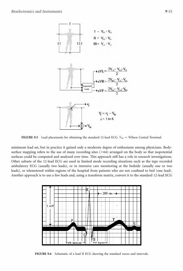
minimum lead set, but in practice it gained only a moderate degree of enthusiasm among physicians. Body-
surface mapping refers to the use of many recording sites (.64) arranged on the body so that isopotential
surfaces could be computed and analyzed over time. This approach still has a role in research investigations.
Other subsets of the 12-lead ECG are used in limited mode recording situations such as the tape recorded
ambulatory ECG (usually two leads), or in intensive care monitoring at the bedside (usually one or two
leads), or telemetered within regions of the hospital from patients who are not confined to bed (one lead).
Another approach is to use a few leads and, using a transform matrix, convert it to the standard 12-lead ECG
FIGURE 9.5 Lead placements for obtaining the standard 12-lead ECG. VW ¼ Wilson Central Terminal.
FIGURE 9.6 Schematic of a lead II ECG showing the standard waves and intervals.
9-15Bioelectronics and Instruments
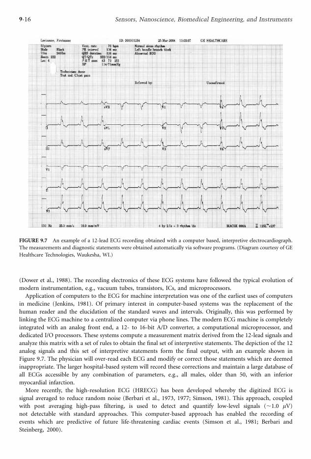
(Dower et al., 1988). The recording electronics of these ECG systems have followed the typical evolution of
modern instrumentation, e.g., vacuum tubes, transistors, ICs, and microprocessors.
Application of computers to the ECG for machine interpretation was one of the earliest uses of computers
in medicine (Jenkins, 1981). Of primary interest in computer-based systems was the replacement of the
human reader and the elucidation of the standard waves and intervals. Originally, this was performed by
linking the ECG machine to a centralized computer via phone lines. The modern ECG machine is completely
integrated with an analog front end, a 12- to 16-bit A/D converter, a computational microprocessor, and
dedicated I/O processors. These systems compute a measurement matrix derived from the 12-lead signals and
analyze this matrix with a set of rules to obtain the final set of interpretive statements. The depiction of the 12
analog signals and this set of interpretive statements form the final output, with an example shown in
Figure 9.7. The physician will over-read each ECG and modify or correct those statements which are deemed
inappropriate. The larger hospital-based system will record these corrections and maintain a large database of
all ECGs accessible by any combination of parameters, e.g., all males, older than 50, with an inferior
myocardial infarction.
More recently, the high-resolution ECG (HRECG) has been developed whereby the digitized ECG is
signal averaged to reduce random noise (Berbari et al., 1973, 1977; Simson, 1981). This approach, coupled
with post averaging high-pass filtering, is used to detect and quantify low-level signals (,1.0 mV)not detectable with standard approaches. This computer-based approach has enabled the recording of
events which are predictive of future life-threatening cardiac events (Simson et al., 1981; Berbari and
Steinberg, 2000).
FIGURE 9.7 An example of a 12-lead ECG recording obtained with a computer based, interpretive electrocardiograph.
The measurements and diagnostic statements were obtained automatically via software programs. (Diagram courtesy of GE
Healthcare Technologies, Waukesha, WI.)
9-16 Sensors, Nanoscience, Biomedical Engineering, and Instruments
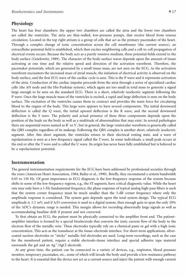
Physiology
The heart has four chambers: the upper two chambers are called the atria and the lower two chambers
are called the ventricles. The atria are thin-walled, low-pressure pumps, that receive blood from venous
circulation. Located in the top right atrium is a group of cells that act as the primary pacemaker of the heart.
Through a complex change of ionic concentration across the cell membranes (the current source), an
extracellular potential field is established, which then excites neighboring cells and a cell-to-cell propagation of
electrical events occurs. Because the body acts as a purely resistive medium, these potential fields extend to the
body surface (Geselowitz, 1989). The character of the body-surface waves depends upon the amount of tissue
activating at one time and the relative speed and direction of the activation wavefront. Therefore, the
pacemaker potentials, which are generated by a small tissue mass, are not seen on the ECG. As the activation
wavefront encounters the increased mass of atrial muscle, the initiation of electrical activity is observed on the
body surface, and the first ECG wave of the cardiac cycle is seen. This is the P wave and it represents activation
of the atria. Conduction of the cardiac impulse proceeds from the atria through a series of specialized cardiac
cells (the AN node and the His-Purkinje system), which again are too small in total mass to generate a signal
large enough to be seen on the standard ECG. There is a short, relatively isoelectric segment following the
P wave. Once the large muscle mass of the ventricles is excited, a rapid and large deflection is seen on the body
surface. The excitation of the ventricles causes them to contract and provides the main force for circulating
blood to the organs of the body. This large wave appears to have several components. The initial downward
deflection is called the Q wave, the initial upward deflection is the R wave, and the second downward
deflection is the S wave. The polarity and actual presence of these three components depends upon the
position of the leads on the body as well as a multitude of abnormalities that may exist. In several pathologies
there are sequential waves named as R 0 or S 0, but in general, the large ventricular waveform is generically called
the QRS complex regardless of its makeup. Following the QRS complex is another short, relatively isoelectric
segment. After this short segment, the ventricles return to their electrical resting state, and a wave of
repolarization is seen as a low-frequency signal called the T wave. In some individuals, a small peak occurs at
the end or after the Twave and is called the U wave. Its origin has never been fully established but is believed to
be a repolarization potential.
Instrumentation
The general instrumentation requirements for the ECG have been addressed by professional societies through
the years (American Heart Association, 1984; Bailey et al., 1990). Briefly, they recommend a system bandwidth
0.05 to 150 Hz. Of great importance in ECG diagnosis is the low-frequency response of the system because
shifts in some of the low-frequency regions, e.g., the ST segment, have critical diagnostic value. While the heart
rate may only have a 1-Hz fundamental frequency, the phase response of typical analog high-pass filters is such
that the system corner frequency must be much smaller than the 3-dB corner frequency where only the
amplitude response is considered. The system gain depends upon the total system design. The typical ECG
amplitude is^2 mV, and if A/D conversion is used in a digital system, then enough gain to span the only 20%
of the ADC’s dynamic range is needed. This margin allows for recording abnormally large signals as well as
accommodating baseline drift if present and not corrected.
To first obtain an ECG, the patient must be physically connected to the amplifier front end. The patient–
amplifier interface is formed by a special bioelectrode that converts the ionic current flow of the body to the
electron flow of the metallic wire. These electrodes typically rely on a chemical paste or gel with a high ionic
concentration. This acts as the transducer at the tissue–electrode interface. For short-term applications, silver-
coated suction electrodes or ‘‘sticky’’ metallic foil electrodes are used. Long-term recordings, such as the case
for the monitored patient, require a stable electrode–tissue interface and special adhesive tape material
surrounds the gel and an Agþ /AgCl electrode.At any given time, the patient can be connected to a variety of devices, e.g., respirator, blood pressure
monitor, temporary pacemaker, etc., some of which will invade the body and provide a low-resistance pathway
to the heart. It is essential that the device not act as a current source and inject the patient with enough current
9-17Bioelectronics and Instruments
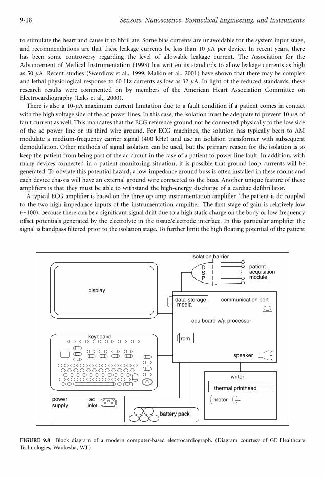
to stimulate the heart and cause it to fibrillate. Some bias currents are unavoidable for the system input stage,
and recommendations are that these leakage currents be less than 10 mA per device. In recent years, there
has been some controversy regarding the level of allowable leakage current. The Association for the
Advancement of Medical Instrumentation (1993) has written its standards to allow leakage currents as high
as 50 mA. Recent studies (Swerdlow et al., 1999; Malkin et al., 2001) have shown that there may be complex
and lethal physiological response to 60 Hz currents as low as 32 mA. In light of the reduced standards, theseresearch results were commented on by members of the American Heart Association Committee on
Electrocardiography (Laks et al., 2000).
There is also a 10-mA maximum current limitation due to a fault condition if a patient comes in contact
with the high voltage side of the ac power lines. In this case, the isolation must be adequate to prevent 10 mA offault current as well. This mandates that the ECG reference ground not be connected physically to the low side
of the ac power line or its third wire ground. For ECG machines, the solution has typically been to AM
modulate a medium-frequency carrier signal (400 kHz) and use an isolation transformer with subsequent
demodulation. Other methods of signal isolation can be used, but the primary reason for the isolation is to
keep the patient from being part of the ac circuit in the case of a patient to power line fault. In addition, with
many devices connected in a patient monitoring situation, it is possible that ground loop currents will be
generated. To obviate this potential hazard, a low-impedance ground buss is often installed in these rooms and
each device chassis will have an external ground wire connected to the buss. Another unique feature of these
amplifiers is that they must be able to withstand the high-energy discharge of a cardiac defibrillator.
A typical ECG amplifier is based on the three op-amp instrumentation amplifier. The patient is dc coupled
to the two high impedance inputs of the instrumentation amplifier. The first stage of gain is relatively low
(,100), because there can be a significant signal drift due to a high static charge on the body or low-frequency
offset potentials generated by the electrolyte in the tissue/electrode interface. In this particular amplifier the
signal is bandpass filtered prior to the isolation stage. To further limit the high floating potential of the patient
display
battery pack
motor
thermal printhead
writer
patientacquisitionmodule
speaker
powersupply
acinlet
communication port
keyboard
...
isolation barrier
data storagemedia
rom
cpu board w/μ processor
DSP
FIGURE 9.8 Block diagram of a modern computer-based electrocardiograph. (Diagram courtesy of GE Healthcare
Technologies, Waukesha, WI.)
9-18 Sensors, Nanoscience, Biomedical Engineering, and Instruments
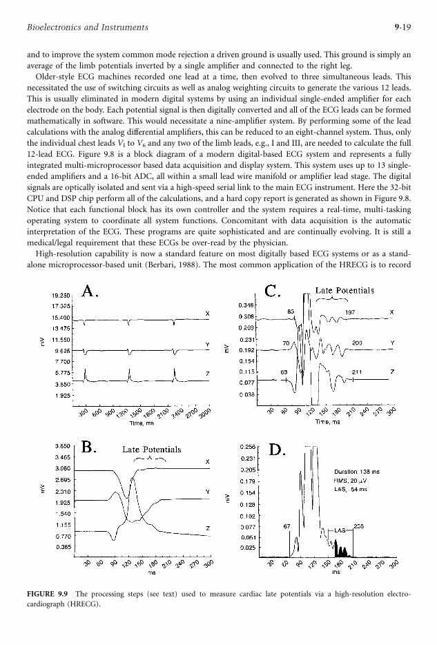
and to improve the system common mode rejection a driven ground is usually used. This ground is simply an
average of the limb potentials inverted by a single amplifier and connected to the right leg.
Older-style ECG machines recorded one lead at a time, then evolved to three simultaneous leads. This
necessitated the use of switching circuits as well as analog weighting circuits to generate the various 12 leads.
This is usually eliminated in modern digital systems by using an individual single-ended amplifier for each
electrode on the body. Each potential signal is then digitally converted and all of the ECG leads can be formed
mathematically in software. This would necessitate a nine-amplifier system. By performing some of the lead
calculations with the analog differential amplifiers, this can be reduced to an eight-channel system. Thus, only
the individual chest leads VI to V6 and any two of the limb leads, e.g., I and III, are needed to calculate the full
12-lead ECG. Figure 9.8 is a block diagram of a modern digital-based ECG system and represents a fully
integrated multi-microprocessor based data acquisition and display system. This system uses up to 13 single-
ended amplifiers and a 16-bit ADC, all within a small lead wire manifold or amplifier lead stage. The digital
signals are optically isolated and sent via a high-speed serial link to the main ECG instrument. Here the 32-bit
CPU and DSP chip perform all of the calculations, and a hard copy report is generated as shown in Figure 9.8.
Notice that each functional block has its own controller and the system requires a real-time, multi-tasking
operating system to coordinate all system functions. Concomitant with data acquisition is the automatic
interpretation of the ECG. These programs are quite sophisticated and are continually evolving. It is still a
medical/legal requirement that these ECGs be over-read by the physician.
High-resolution capability is now a standard feature on most digitally based ECG systems or as a stand-
alone microprocessor-based unit (Berbari, 1988). The most common application of the HRECG is to record
FIGURE 9.9 The processing steps (see text) used to measure cardiac late potentials via a high-resolution electro-
cardiograph (HRECG).
9-19Bioelectronics and Instruments
very low-level (,1.0 mV) signals, which occur after the QRS complex, but are not evident on the standardECG. These ‘‘late potentials’’ are generated from abnormal regions of the ventricles and have been strongly
associated with the substrate responsible for a life-threatening rapid heart rate (ventricular tachycardia). The
typical HRECG is derived from three bipolar leads configured in an anatomic XYZ coordinate system.
These three ECG signals are then digitized at a rate of 1000 to 2000 Hz/channel, time aligned via a real-time
QRS correlator, and summated in the form of a signal average. Signal averaging will theoretically improve the
signal-to-noise ratio by the square root of the number of beats averaged. The underlying assumptions are that
the signals of interest do not vary, on a beat-to-beat basis, and that the noise is random. Figure 9.9 has four
panels depicting the most common sequence for processing the HRECG to measure the late potentials. Panel
A depicts a 3-sec recording of the XYZ leads close to normal resolution. Panel B was obtained after averaging
200 beats and with a sampling frequency of ten times that shown in panel A. The gain is also 5 times greater.
Panel C is the high-pass filtered signal using a partially time reversed digital filter having a second-order
Butterworth response and a 3-dB corner frequency of 40 Hz (Simson, 1981). Note the appearance of the
signals at the terminal portion of the QRS complex. A common method of analysis, but necessarily optimal, is
to combine the filtered XYZ leads into a vector magnitude (X2 þ Y2 þ Z2)1/2. This waveform is shown in panel
D. From this waveform, several parameters have been derived such as total QRS duration, including late
potentials, the rms voltage value of the terminal 40 ms, and the low-amplitude signal (LAS) duration from the
40-mV level to the end of the late potentials. Abnormal values for these parameters are used to identify patientsat high risk of ventricular tachycardia following a heart attack.
Conclusions
The ECG is one of the oldest instrument-bound measurements in medicine. It has faithfully followed the
progression of instrumentation technology. Its most recent evolutionary step, to the microprocessor-based
system, has allowed for an enhanced, high-resolution ECG, which has opened new vistas of ECG analysis and
interpretation.
Defining Terms
12-lead ECG: Twelve traditional ECG leads comprising the standard set.
ECG: Abbreviation for the device (electrocardiograph) or the output (electrocardiogram) depicting the
body surface recording of the electrical activity of the heart.
ECG lead: Differential signal depicting one channel of the ECG record.
HRECG: High-resolution ECG used to detect microvolt-level cardiac potentials most commonly by signal
averaging.
Wilson central terminal: Reference point for forming most of the standard ECG leads. It is the average of
the right arm, left arm, and left leg potentials. It is a time-varying reference.
References
J.J. Bailey, A.S. Berson, A. Carson, L.G. Horan, P.W. Macfarlane, D.W. Mortara, and C. Zywietz,
‘‘Recommendations for standardization and specifications in automated electrocardiography:
bandwidth and digital signal processing,’’ A report for health professionals by an ad hoc writing
group of the Committee on Electrocardiography and Cardiac Electrophysiology of the Council on
Clinical Cardiology, American Heart Association, Circulation, vol. 81, no. 2, pp. 730–739, 1990.
E.J. Berbari, R. Lazzara, P. Samet, and B.J. Scherlag, ‘‘Noninvasive technique for detection of electrical activity
during the PR segment,’’ Circulation, vol. 48, p. 1006, 1973.
E.]. Berbari, R. Lazzara, and B.J. Scherlag, ‘‘A computerized technique to record new components of the
electrocardiogram,’’ Proc. IEEE, vol. 65, p. 799, 1977.
E.J. Berbari, B.J. Scherlag, R.R. Hope, and R. Lazzara, ‘‘Recording from the body surface of arrhythmogenic
ventricular activity during the ST segment,’’ Am. J. Cardiol., vol. 41, p. 697, 1978.
9-20 Sensors, Nanoscience, Biomedical Engineering, and Instruments

G.E. Dower, A. Yakush, S.B. Nazzal, R.V. Jutzy, and C.E. Ruiz, ‘‘Deriving the 12-lead electrocardiogram from
four (EASI) electrodes,’’ J. Electrocardiol., vol. 21, Suppl. S182-7, 1988.
W. Einthoven, ‘‘Die galvanometrische Registrirung des menschlichen Elektrokardiogramms, zugleich eine
Beurtheilung der Anwendung des Capillar-Elecktrometers in der Physiologic,’’ Pflugers Arch. Gas.
Physiol., vol. 99, p. 472, 1903.
D.B. Geselowitz, ‘‘On the theory of the electrocardiogram,’’ Proc. IEEE, vol. 77, p. 857, 1989.
E. Goldberger, ‘‘A simple, indifferent, electrocardiographic electrode of zero potential and a technique of
obtaining augmented, unipolar, extremity leads,’’ Am. Heart J., vol. 23, p. 483, 1942.
J.M. Jenkins, ‘‘Computerized electrocardiography,’’ CRC Crit. Rev. Bioeng., vol. 6, p. 307, 1981.
R.A. Malkin and B.K. Hoffmeister, ‘‘Mechanisms by which AC leakage currents cause complete hemodynamic
collapse without inducing fibrillation. [see comment],’’ J. Cardiovasc. Electrophysiol., vol. 12, no. 10,
pp. 1154–1161, 2001.
M.M. Laks, R. Arzbaecher, D. Geselowitz, J.J Bailey, and A. Berson, ‘‘Revisiting the question: will relaxing safe
current limits for electromedical equipment increase hazards to patients?,’’ Circulation vol. 102, no. 8,
823–825, 2000 Aug 22
M.B. Simson, ‘‘Use of signals in the terminal QRS complex to identify patients with ventricular tachycardia
after myocardial infarction,’’ Circulation, vol. 64, p. 235, 1981.
C.D. Swerdlow, W.H. Olson, M.E. O’Connor, et al., ‘‘Cardiovascular collapse caused by electrocardiographi-
cally silent 60 Hz intracardiac leakage current: implications for electrical safety,’’ Circulation, vol. 99,
pp. 2559–2564, 1999.
Safe Current Limits for Electromedical Apparatus: American National Standard, ANSI/AAMI ES1–1993.
Arlington, VA: Association for the Advancement of Medical Instrumentation; 1993.
A.D. Waller, ‘‘On the electromotive changes connected with the beat of the mammalian heart, and the human
heart in particular,’’ Phil. Trans. B., vol. 180, p. 169, 1889.
E.N. Wilson, F.S. Johnston, and I.G.W. Hill, ‘‘The interpretation of the galvanometric curves obtained when
one electrode is distant from the heart and the other near or in contact with the ventricular surface,’’
Am. Heart J., vol. 10, p. 176, 1934.
Further Information
P.W. Macfarlane and T.D. Veitch Lawrie, Eds., Comprehensive EIectrocardiology: Theory and Practice in Health
and Disease, Volumes 1–3, Oxford: Pergamon Press, 1989.
E.J. Berbari and J.S. Steinberg, A Practical Guide to High Resolution Electrocardiography, Armonk, NY: Futura
Publishers, 2000.
Webter, J.G., Ed., Medical Instrumentation: Application and Design, 3rd ed., Boston, MA: Houghton Mifflin,
1998.
9-21Bioelectronics and Instruments

10Tomography
Martin D. FoxUniversity of Connecticut
10.1 Computerized Tomography ................................................ 10-1
10.2 Positron Emission Tomography .......................................... 10-3
10.3 Single Photon Emission Computed Tomography................... 10-4
10.4 Magnetic Resonance Imaging ............................................. 10-4
10.5 Imaging ........................................................................... 10-5
The term tomography derives from the Greek tomos (cutting) and grapho (to write). Originally the term was
applied to sectional radiography achieved by a synchronous motion of the x-ray source and detector in order
to blur undesired data while creating a sharp image of the selected plane. The term tomography was used to
distinguish between such slices and the more conventional plain film radiograph, which represents a two-
dimensional shadowgraphic superposition of all x-ray absorbing structures within a volumetric body.
Computerized tomography, also known as computerized axial tomography, was introduced by EMI Ltd. in
1973 and transformed medical imaging by obviating the superposition of intervening structures present in
conventional radiographic images. Initially, the clinical application was for imaging the head, but soon the
technique found wide application in body imaging.
As medical imaging has evolved into a multimodality field, the meaning of tomography has broadened to
include any images of thin cross-sectional slices, regardless of the modality utilized to produce them. Thus,
tomographic images can be generated by magnetic resonance imaging (MRI), ultrasound (US),
computerized tomography (CT), or such nuclear medicine techniques as positron emission tomography
(PET) or single photon emission computerized tomography (SPECT). For the purposes of this discussion
we will cover all of the foregoing modalities with the exception of ultrasound, which will be treated separately.
Since the power of such computerized techniques was recognized, the practice of radiology has been
revolutionized by making possible much more precise diagnosis of a wide range of conditions. In this
necessarily brief discussion we will describe the basic physical principles of the major tomographic modalities
as well as their key clinical applications.
10.1 Computerized Tomography
The basic concept of computerized tomography can be described by consideration of Figure 10.1. An x-ray
source is passed through an aperture to produce a fan-shaped beam that passes through the body of interest
with absorption along approximately parallel lines. The natural logarithm of the detected intensity will be the
integral of the linear attenuation coefficient of the object along the ray directed from the source to the detector
element. If the source and the detector array are synchronously rotated about a point within the object,
a number of lines of data can be collected, each representing the projected density of the object as a function of
lateral position and angle.
A number of mathematical techniques can and have been used to recover the two-dimensional distribution
of the linear attenuation coefficient from this array of measurements. These include iterative solution of a set
of simultaneous linear equations, Fourier transform approaches, and techniques utilizing back-projection
10-1
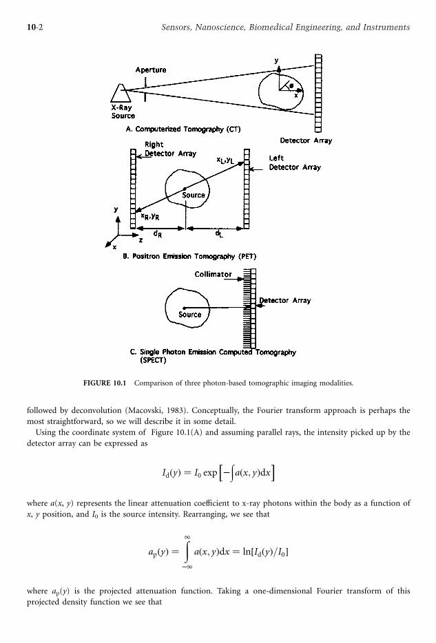
followed by deconvolution (Macovski, 1983). Conceptually, the Fourier transform approach is perhaps the
most straightforward, so we will describe it in some detail.
Using the coordinate system of Figure 10.1(A) and assuming parallel rays, the intensity picked up by the
detector array can be expressed as
IdðyÞ ¼ I0 exph Z
aðx; yÞdxi
where a(x, y) represents the linear attenuation coefficient to x-ray photons within the body as a function of
x, y position, and I0 is the source intensity. Rearranging, we see that
apðyÞ ¼Z11aðx; yÞdx ¼ ln½IdðyÞ=I0
where ap(y) is the projected attenuation function. Taking a one-dimensional Fourier transform of this
projected density function we see that
FIGURE 10.1 Comparison of three photon-based tomographic imaging modalities.
10-2 Sensors, Nanoscience, Biomedical Engineering, and Instruments
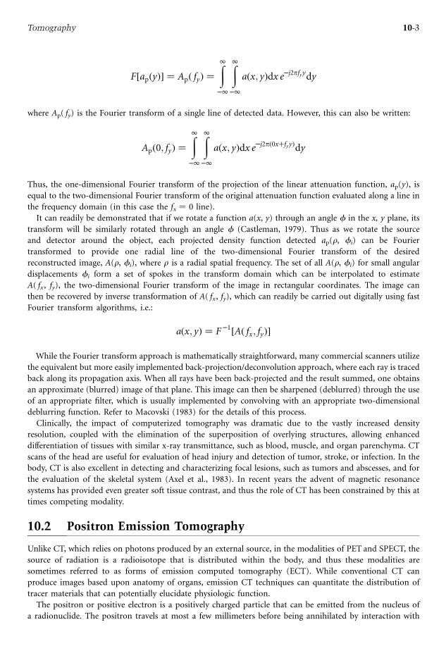
F½apðyÞ ¼ Apð fyÞ ¼Z11
Z11aðx; yÞdx e j2pfyydy
where Ap( fy) is the Fourier transform of a single line of detected data. However, this can also be written:
Apð0; fyÞ ¼Z11
Z11aðx; yÞdx e j2pð0xþfyyÞdy
Thus, the one-dimensional Fourier transform of the projection of the linear attenuation function, ap(y), is
equal to the two-dimensional Fourier transform of the original attenuation function evaluated along a line in
the frequency domain (in this case the fx ¼ 0 line).
It can readily be demonstrated that if we rotate a function a(x, y) through an angle f in the x, y plane, its
transform will be similarly rotated through an angle f (Castleman, 1979). Thus as we rotate the source
and detector around the object, each projected density function detected ap(r, fi) can be Fourier
transformed to provide one radial line of the two-dimensional Fourier transform of the desired
reconstructed image, A(r, fi), where r is a radial spatial frequency. The set of all A(r, fi) for small angulardisplacements fi form a set of spokes in the transform domain which can be interpolated to estimate
A( fx, fy), the two-dimensional Fourier transform of the image in rectangular coordinates. The image can
then be recovered by inverse transformation of A( fx, fy), which can readily be carried out digitally using fast
Fourier transform algorithms, i.e.:
aðx; yÞ ¼ F 1½Að fx; fyÞ
While the Fourier transform approach is mathematically straightforward, many commercial scanners utilize
the equivalent but more easily implemented back-projection/deconvolution approach, where each ray is traced
back along its propagation axis. When all rays have been back-projected and the result summed, one obtains
an approximate (blurred) image of that plane. This image can then be sharpened (deblurred) through the use
of an appropriate filter, which is usually implemented by convolving with an appropriate two-dimensional
deblurring function. Refer to Macovski (1983) for the details of this process.
Clinically, the impact of computerized tomography was dramatic due to the vastly increased density
resolution, coupled with the elimination of the superposition of overlying structures, allowing enhanced
differentiation of tissues with similar x-ray transmittance, such as blood, muscle, and organ parenchyma. CT
scans of the head are useful for evaluation of head injury and detection of tumor, stroke, or infection. In the
body, CT is also excellent in detecting and characterizing focal lesions, such as tumors and abscesses, and for
the evaluation of the skeletal system (Axel et al., 1983). In recent years the advent of magnetic resonance
systems has provided even greater soft tissue contrast, and thus the role of CT has been constrained by this at
times competing modality.
10.2 Positron Emission Tomography
Unlike CT, which relies on photons produced by an external source, in the modalities of PET and SPECT, the
source of radiation is a radioisotope that is distributed within the body, and thus these modalities are
sometimes referred to as forms of emission computed tomography (ECT). While conventional CT can
produce images based upon anatomy of organs, emission CT techniques can quantitate the distribution of
tracer materials that can potentially elucidate physiologic function.
The positron or positive electron is a positively charged particle that can be emitted from the nucleus of
a radionuclide. The positron travels at most a few millimeters before being annihilated by interaction with
10-3Tomography
a negative electron from the surrounding tissue. The product of this event is the emission of 511-keV gamma-
ray photons which travel in almost exactly opposite directions. The detectors themselves can be either discrete
detectors or a modified Anger camera like those used in conventional nuclear imaging. A coincidence detector
is employed to limit recorded outputs to cases in which events are detected simultaneously in both detector
arrays, thus reducing the pickup of noise or scattering.
A possible detection scheme is illustrated in Figure 10.1(B). The detector arrays shown can be made energy
selective to eliminate lower energy scattered gamma rays. While the distribution of radioactivity can be
reconstructed using the reconstruction from projection techniques described in the section on CT (Hurculak,
1987), the x, y source position of an event can be determined directly from the detection geometry as follows
(Macovski, 1983):
x < xLdR=ðdR þ dLÞ þ xRdL=ðdR þ dLÞy < yLdR=ðdR þ dLÞ þ yRdL=ðdR þ dLÞ
Typically a single plane is studied, and no collimators are required. A drawback of PET has been that
because of the short half-lives of positron-producing radioisotopes, the use of this modality has required the
presence of an expensive cyclotron facility located near the hospital.
One important radionuclide commonly used in PET is oxygen 15 with a half-life of 2.07 min, which can be
bonded to water for measurement of cerebral blood flow or to O2/CO2 to assess cerebral oxygen utilization.
Another is carbon 11 with a half-life of 20.4 min, which can be bonded to glucose to trace glucose
utilization. F-18 fluorodeoxyglucose (FDG) has been used to demonstrate the degree of malignancy of primary
brain tumors, to distinguish necrosis from tumor, and to predict outcome (Coleman, 1991). Perhaps the most
unusual feature of this modality is the ability to quantitate the regional metabolism of the human heart
(Schelbert, 1990).
10.3 Single Photon Emission Computed Tomography
In contrast to PET, SPECT can be utilized with any radioisotope that emits gamma rays, including such
common radioisotopes as Tc-99m, I-125, and I-131 which have been utilized in conventional nuclear imaging
for the last 30 to 35 years and which due to their relatively long half-lives are available at reasonable cost at
nearly every modern hospital. Because of the need for direction sensitivity of the detector, a collimator must be
used to eliminate gamma rays from other than the prescribed direction, thus resulting in a 1 to 2 order of
magnitude decrease in quantum efficiency as compared with PET scanning (Knoll, 1983).
The basic concept of SPECT is illustrated in Figure 10.1(C). A gamma ray photon from a radionuclide with
energy above 100 keV will typically escape from the body without further interaction, and thus the body can
be regarded as a transparent object with luminosity proportional to the concentration of the radionuclide at
each point. The reconstruction mathematics are similar to those derived for absorption CT, with the exception
that the variable reconstructed is a source distribution rather than an attenuation coefficient. Some errors can
be introduced in the reconstruction because of the inevitable interaction of gamma rays with overlying tissue,
even at energies above 100 keV, although this can be compensated for to some extent. Detection of scattered
radiation can be reduced through the use of an energy acceptance window in the detector.
Technetium 99m can be used to tag red blood cells for blood pool measurements, human serum albumin
for blood pool and protein distribution, or monoclonal antibodies for potential detection of individual
tumors or blood cells. ECT techniques such as PET and SPECT follow the recent trend toward imaging
techniques that image physiologic processes as opposed to anatomic imaging of organ systems. The relatively
low cost of SPECT systems has led to a recent resurgence of interest in this modality.
10.4 Magnetic Resonance Imaging
The basic magnetic resonance concept has been used as a tool in chemistry and physics since its discovery by
Bloch in 1946, but its use expanded tremendously in the 1980s with the development of means to represent
10-4 Sensors, Nanoscience, Biomedical Engineering, and Instruments
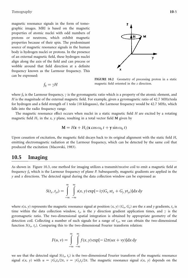
magnetic resonance signals in the form of tomo-
graphic images. MRI is based on the magnetic
properties of atomic nuclei with odd numbers of
protons or neutrons, which exhibit magnetic
properties because of their spin. The predominant
source of magnetic resonance signals in the human
body is hydrogen nuclei or protons. In the presence
of an external magnetic field, these hydrogen nuclei
align along the axis of the field and can precess or
wobble around that field direction at a definite
frequency known as the Larmour frequency. This
can be expressed:
f0 ¼ gH
where f0 is the Larmour frequency, g is the gyromagnetic ratio which is a property of the atomic element, andH is the magnitude of the external magnetic field. For example, given a gyromagnetic ratio of 42.7 MHz/tesla
for hydrogen and a field strength of 1 tesla (10 kilogauss), the Larmour frequency would be 42.7 MHz, which
falls into the radio frequency range.
The magnetic resonance effect occurs when nuclei in a static magnetic field H are excited by a rotating
magnetic field H1 in the x, y plane, resulting in a total vector field M given by
M ¼ HzþH1ðx coso0 t þ y sino0 tÞ
Upon cessation of excitation, the magnetic field decays back to its original alignment with the static field H,
emitting electromagnetic radiation at the Larmour frequency, which can be detected by the same coil that
produced the excitation (Macovski, 1983).
10.5 Imaging
As shown in Figure 10.3, one method for imaging utilizes a transmit/receive coil to emit a magnetic field at
frequency f0 which is the Larmour frequency of plane P. Subsequently, magnetic gradients are applied in the
y and x directions. The detected signal during the data collection window can be expressed as
Sðtx; tyiÞ ¼Z11
Z11sðx; yÞ exp½ igðGx xtx þ Gy ytyiÞ dx dy
where s(x, y) represents the magnetic resonance signal at position (x, y) (Gx, Gy) are the x and y gradients, tx is
time within the data collection window, tyi is the y direction gradient application times, and g is the
gyromagnetic ratio. The two-dimensional spatial integration is obtained by appropriate geometry of the
detection coil. Collecting a number of such signals for a range of tyi, we can obtain the two-dimensional
function S(tx, ty). Comparing this to the two-dimensional Fourier transform relation:
Fðu; vÞ ¼Z11
Z11f ðx; yÞ exp½ i2pðux þ vyÞ dx dy
we see that the detected signal S(tx, ty) is the two-dimensional Fourier transform of the magnetic resonance
signal s(x, y) with u ¼ gGxtx/2p, v ¼ gGyty/2p. The magnetic resonance signal s(x, y) depends on the
FIGURE 10.2 Geometry of precessing proton in a static
magnetic field oriented in the z direction.
10-5Tomography
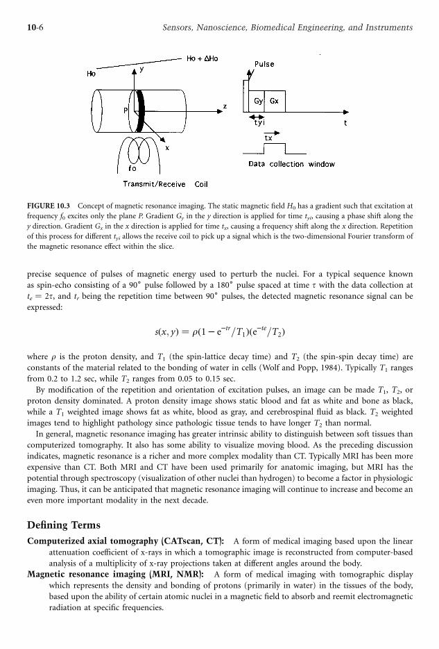
precise sequence of pulses of magnetic energy used to perturb the nuclei. For a typical sequence known
as spin-echo consisting of a 90– pulse followed by a 180– pulse spaced at time t with the data collection atte ¼ 2t, and tr being the repetition time between 90– pulses, the detected magnetic resonance signal can beexpressed:
sðx; yÞ ¼ rð1 e tr=T1Þðe te=T2Þ
where r is the proton density, and T1 (the spin-lattice decay time) and T2 (the spin-spin decay time) are
constants of the material related to the bonding of water in cells (Wolf and Popp, 1984). Typically T1 ranges
from 0.2 to 1.2 sec, while T2 ranges from 0.05 to 0.15 sec.
By modification of the repetition and orientation of excitation pulses, an image can be made T1, T2, or
proton density dominated. A proton density image shows static blood and fat as white and bone as black,
while a T1 weighted image shows fat as white, blood as gray, and cerebrospinal fluid as black. T2 weighted
images tend to highlight pathology since pathologic tissue tends to have longer T2 than normal.
In general, magnetic resonance imaging has greater intrinsic ability to distinguish between soft tissues than
computerized tomography. It also has some ability to visualize moving blood. As the preceding discussion
indicates, magnetic resonance is a richer and more complex modality than CT. Typically MRI has been more
expensive than CT. Both MRI and CT have been used primarily for anatomic imaging, but MRI has the
potential through spectroscopy (visualization of other nuclei than hydrogen) to become a factor in physiologic
imaging. Thus, it can be anticipated that magnetic resonance imaging will continue to increase and become an
even more important modality in the next decade.
Defining Terms
Computerized axial tomography (CATscan, CT): A form of medical imaging based upon the linear
attenuation coefficient of x-rays in which a tomographic image is reconstructed from computer-based
analysis of a multiplicity of x-ray projections taken at different angles around the body.
Magnetic resonance imaging (MRI, NMR): A form of medical imaging with tomographic display
which represents the density and bonding of protons (primarily in water) in the tissues of the body,
based upon the ability of certain atomic nuclei in a magnetic field to absorb and reemit electromagnetic
radiation at specific frequencies.
FIGURE 10.3 Concept of magnetic resonance imaging. The static magnetic field H0 has a gradient such that excitation at
frequency f0 excites only the plane P. Gradient Gy in the y direction is applied for time tyi, causing a phase shift along the
y direction. Gradient Gx in the x direction is applied for time tx, causing a frequency shift along the x direction. Repetition
of this process for different tyi allows the receive coil to pick up a signal which is the two-dimensional Fourier transform of
the magnetic resonance effect within the slice.
10-6 Sensors, Nanoscience, Biomedical Engineering, and Instruments

Positron emission tomography (PET scan): A form of tomographic medical imaging based upon the
density of positron-emitting radionuclides in an object.
Single photon emission computed tomography (SPECT): A form of tomographic medical imaging
based upon the density of gamma ray-emitting radionuclides in the body.
Tomography: A method of image presentation in which the data is displayed in the form of individual
slices that represent planar sections of the object.
References
L. Axel, P.H. Arger, and R. Zimmerman, ‘‘Applications of computerized tomography to diagnostic radiology,’’
in Proc. IEEE, vol. 71, no. 3, p. 293, 1983.
K.R. Castleman, Digital Image Processing, Englewood Cliffs, NJ: Prentice-Hall, 1979.
R.E. Coleman, ‘‘Single photon emission computed tomography and positron emission tomography,’’ Cancer,
vol. 67 (4 Suppl.), pp. 1261–1270, 1991.
P.M. Hurculak, ‘‘Positron emission tomography,’’ Can. J. Med. Radiat. Technol., vol. 18, no. 1, 1987.
G.F. Knoll, ‘‘Single-photon emission computed tomography,’’ Proc. IEEE, vol. 71, no. 3, p. 320, 1983.
A. Macovski, Medical Imaging Systems, Englewood Cliffs, NJ: Prentice-Hall, 1983.
H.R. Schelbert, ‘‘Future perspectives: Diagnostic possibilities with positron emission tomography,’’ Roentgen
Blaetter, vol. 43, no. 9, pp. 384–390, 1990.
G.L. Wolf and C. Popp, NMR, A Primer for Medical Imaging, Thorofare, NJ: Slack, Inc., 1984.
Further Information
The journal IEEE Transactions on Medical Imaging describes advances in imaging techniques and image
processing. Investigative Radiology, published by the Association of University Radiologists, emphasizes
research carried out by hospital-based physicists and engineers. Radiology, published by the North American
Society of Radiologists, contains articles which emphasize clinical applications of imaging technology. Diag-
nostic Imaging, publishing by Miller Freeman, Inc., is a good source of review articles and information on the
imaging marketplace
10-7Tomography


IIIMathematics, Symbols,and Physical Constants
Greek Alphabet ......................................................................................................................... III-3
International System of Units (SI) ......................................................................................... III-3
Definitions of SI Base Units * Names and Symbols for the SI Base Units *
SI Derived Units with Special Names and Symbols *
Units in Use Together with the SI
Conversion Constants and Multipliers ................................................................................. III-6
Recommended Decimal Multiples and Submultiples * Conversion Factors—Metric
to English * Conversion Factors—English to Metric * Conversion Factors—General *
Temperature Factors * Conversion of Temperatures
Physical Constants ..................................................................................................................... III-8
General * p Constants * Constants Involving e * Numerical Constants
Symbols and Terminology for Physical and Chemical Quantities .................................... III-9
Classical Mechanics * Electricity and Magnetism * Electromagnetic Radiation *
Solid State
Credits ...................................................................................................................................... III-13
Probability for Electrical and Computer Engineers Charles W. Therrien ................... III-14
The Algebra of Events * Probability * An Example * Conditional Probability
and Bayes’ Rule * Communication Example
Ronald J. TallaridaTemple University
THE GREATACHIEVEMENTS in engineering deeply affect the lives of all of us and also serve to remind us of
the importance of mathematics. Interest in mathematics has grown steadily with these engineering
achievements and with concomitant advances in pure physical science. Whereas scholars in nonscientific
fields, and even in such fields as botany, medicine, geology, etc., can communicate most of the problems and
results in nonmathematical language, this is virtually impossible in present-day engineering and physics. Yet it
is interesting to note that until the beginning of the twentieth century, engineers regarded calculus as
something of a mystery. Modern students of engineering now study calculus, as well as differential equations,
complex variables, vector analysis, orthogonal functions, and a variety of other topics in applied analysis. The
study of systems has ushered in matrix algebra and, indeed, most engineering students now take linear algebra
as a core topic early in their mathematical education.
III-1

This section contains concise summaries of relevant topics in applied engineering mathematics and certain
key formulas, that is, those formulas that are most often needed in the formulation and solution of
engineering problems. Whereas even inexpensive electronic calculators contain tabular material (e.g., tables of
trigonometric and logarithmic functions) that used to be needed in this kind of handbook, most calculators
do not give symbolic results. Hence, we have included formulas along with brief summaries that guide their
use. In many cases we have added numerical examples, as in the discussions of matrices, their inverses, and
their use in the solutions of linear systems. A table of derivatives is included, as well as key applications of the
derivative in the solution of problems in maxima and minima, related rates, analysis of curvature, and finding
approximate roots by numerical methods. A list of infinite series, along with the interval of convergence of
each, is also included.
Of the two branches of calculus, integral calculus is richer in its applications, as well as in its theoretical
content. Though the theory is not emphasized here, important applications such as finding areas, lengths,
volumes, centroids, and the work done by a nonconstant force are included. Both cylindrical and spherical
polar coordinates are discussed, and a table of integrals is included. Vector analysis is summarized in a separate
section and includes a summary of the algebraic formulas involving dot and cross multiplication, frequently
needed in the study of fields, as well as the important theorems of Stokes and Gauss. The part on special
functions includes the gamma function, hyperbolic functions, Fourier series, orthogonal functions, and both
Laplace and z-transforms. The Laplace transform provides a basis for the solution of differential equations and
is fundamental to all concepts and definitions underlying analytical tools for describing feedback control
systems. The z-transform, not discussed in most applied mathematics books, is most useful in the analysis of
discrete signals as, for example, when a computer receives data sampled at some prespecified time interval. The
Bessel functions, also called cylindrical functions, arise in many physical applications, such as the heat transfer
in a ‘‘long’’ cylinder, whereas the other orthogonal functions discussed—Legendre, Hermite, and Laguerre
polynomials—are needed in quantum mechanics and many other subjects (e.g., solid-state electronics) that
use concepts of modern physics.
The world of mathematics, even applied mathematics, is vast. Even the best mathematicians cannot keep up
with more than a small piece of this world. The topics included in this section, however, have withstood the
test of time and, thus, are truly core for the modern engineer.
This section also incorporates tables of physical constants and symbols widely used by engineers. While not
exhaustive, the constants, conversion factors, and symbols provided will enable the reader to accommodate a
majority of the needs that arise in design, test, and manufacturing functions.
III-2 Mathematics, Symbols, and Physical Constants

Mathematics,Symbols, and
Physical Constants
Greek Alphabet
International System of Units (SI)
The International System of units (SI) was adopted by the 11th General Conference on Weights and Measures
(CGPM) in 1960. It is a coherent system of units built form seven SI base units, one for each of the seven
dimensionally independent base quantities: they are the meter, kilogram, second, ampere, kelvin, mole, and
candela, for the dimensions length, mass, time, electric current, thermodynamic temperature, amount of
substance, and luminous intensity, respectively. The definitions of the SI base units are given below. The SI
derived units are expressed as products of powers of the base units, analogous to the corresponding relations
between physical quantities but with numerical factors equal to unity.
In the International System there is only one SI unit for each physical quantity. This is either the appropriate
SI base unit itself or the appropriate SI derived unit. However, any of the approved decimal prefixes, called SI
prefixes, may be used to construct decimal multiples or submultiples of SI units.
It is recommended that only SI units be used in science and technology (with SI prefixes where
appropriate). Where there are special reasons for making an exception to this rule, it is recommended always
to define the units used in terms of SI units. This section is based on information supplied by IUPAC.
Definitions of SI Base Units
Meter: The meter is the length of path traveled by light in vacuum during a time interval of 1/299,792,458
of a second (17th CGPM, 1983).
Kilogram: The kilogram is the unit of mass; it is equal to the mass of the international prototype of the
kilogram (3rd CGPM, 1901).
Second: The second is the duration of 9,192,631,770 periods of the radiation corresponding to the
transition between the two hyperfine levels of the ground state of the cesium-133 atom (13th CGPM, 1967).
Greek
Letter
Greek
Name
English
Equivalent
Greek
Letter
Greek
Name
English
Equivalent
A a Alpha a N n Nu n
B b Beta b X j Xi x
G g Gamma g O o Omicron o
D d Delta d Q p Pi P
E e Epsilon e P r Rho r
Z z Zeta z S s Sigma s
H Z Eta e T t Tau t
Y y q Theta th Y y Upsilon u
I i Iota i F f j Phi ph
K k Kappa k X w Chi ch
L l Lambda l C c Psi ps
M m Mu m O o Omega o
III-3Mathematics, Symbols, and Physical Constants

Ampere: The ampere is that constant current which, if maintained in two straight parallel conductors of
infinite length, of negligible circular cross-section, and placed 1 m apart in vacuum, would produce between
these conductors a force equal to 2 · 10 7 newton per meter of length (9th CGPM, 1948).
Kelvin: The kelvin, unit of thermodynamic temperature, is the fraction 1/273.16 of the thermodynamic
temperature of the triple point of water (13th CGPM, 1967).
Mole: The mole is the amount of substance of a system which contains as many elementary entities as there
are atoms in 0.012 kg of carbon-12. When the mole is used, the elementary entities must be specified and may
be atoms, molecules, ions, electrons, or other particles or specified groups of such particles (14th CGPM,
1971).
Examples of the use of the mole:
1 mol of H2 contains about 6.022 · 1023 H2 molecules, or 12.044 · 1023 H atoms.
1 mol of HgCl has a mass of 236.04 g.
1 mol of Hg2Cl2 has a mass of 472.08 g.
1 mol of Hg22þ has a mass of 401.18 g and a charge of 192.97 kC.
1 mol of Fe0.91S has a mass of 82.88 g.
1 mol of e has a mass of 548.60 mg and a charge of 96.49 kC.
1 mol of photons whose frequency is 1014 Hz has energy of about 39.90 kJ.
Candela: The candela is the luminous intensity in a given direction of a source that emits monochromatic
radiation of frequency 540 · 1012 hertz and that has a radiant intensity in that direction of (1/683) watt persteradian (16th CGPM, 1979).
Physical Quantity Name of SI Unit Symbol for SI Unit
Length meter m
Mass kilogram kg
Time second s
Electric current ampere A
Thermodynamic temperature kelvin K
Amount of substance mole mol
Luminous intensity candela cd
Names and Symbols for the SI Base Units
Physical Quantity
Name of
SI Unit
Symbol for
SI Unit
Expression in
Terms of SI Base Units
Frequency1 hertz Hz s 1
Force newton N m kg s 2
Pressure, stress pascal Pa N m 2 ¼ m 1 kg s 2
Energy, work, heat joule J N m ¼ m2 kg s 2
Power, radiant flux watt W J s 1 ¼ m2 kg s 3
Electric charge coulomb C A s
Electric potential,
electromotive force
volt V J C 1 ¼ m2 kg s 3 A 1
Electric resistance ohm O V A 1 ¼ m2 kg s 3 A 2
Electric conductance siemens S O 1 ¼ m 2 kg 1 s3 A2
Electric capacitance farad F C V 1 ¼ m 2 kg 1 s4 A2
Magnetic flux density tesla T V s m 2 ¼ kg s 2 A 1
Magnetic flux weber Wb V s ¼ m2 kg s 2 A 1
Inductance henry H V A 1 s ¼ m2 kg s 2 A 2
Celsius temperature2 degree Celsius –C K
(continued)
SI Derived Units with Special Names and Symbols
III-4 Mathematics, Symbols, and Physical Constants

Units in Use Together with the SI
These units are not part of the SI, but it is recognized that they will continue to be used in appropriate
contexts. SI prefixes may be attached to some of these units, such as milliliter, ml; millibar, mbar;
megaelectronvolt, MeV; kilotonne, ktonne.
SI Derived Units with Special Names and Symbols (continued)
Physical Quantity
Name of
SI Unit
Symbol for
SI Unit
Expression in
Terms of SI Base Units
Luminous flux lumen lm cd sr
Illuminance lux lx cd sr m 2
Activity (radioactive) becquerel Bq s 1
Absorbed dose (of radiation) gray Gy J kg 1 ¼ m2 s 2
Dose equivalent
(dose equivalent index)
sievert Sv J kg 1 ¼ m2 s 2
Plane angle radian rad 1 ¼ m m 1
Solid angle steradian sr 1 ¼ m2 m 2
1For radial (circular) frequency and for angular velocity the unit rad s 1, or simply s 1, should be used,and this may not be simplified to Hz. The unit Hz should be used only for frequency in the sense of cyclesper second.
2The Celsius temperature y is defined by the equation:
y=–C ¼ T=K 273:15
The SI unit of Celsius temperature interval is the degree Celsius, –C, which is equal to the kelvin, K. –Cshould be treated as a single symbol, with no space between the – sign and the letter C. (The symbol –K andthe symbol – should no longer be used.)
Physical
Quantity Name of Unit
Symbol
for Unit Value in SI Units
Time minute min 60 s
Time hour h 3600 s
Time day d 86,400 s
Plane angle degree – (p/180) radPlane angle minute 0 (p/10,800) radPlane angle second 00 (p/648,000) radLength angstrom1 A 10 10 m
Area barn b 10 28 m2
Volume liter l, L dm3 ¼ 10 3 m3
Mass tonne t Mg ¼ 103 kg
Pressure bar1 bar 105 Pa ¼ 105 N m 2
Energy electronvolt2 eV (¼ e · V) <1.60218 · 10 19 J
Mass unified atomic mass unit2,3 u (¼ma(12C)/12) <1.66054 · 10 27 kg
1The angstrom and the bar are approved by CIPM for ‘‘temporary use with SI units,’’ until CIPMmakes a further recommendation. However, they should not be introduced where they are not usedat present.
2The values of these units in terms of the corresponding SI units are not exact, since they dependon the values of the physical constants e (for the electronvolt) and Na (for the unified atomic massunit), which are determined by experiment.
3The unified atomic mass unit is also sometimes called the dalton, with symbol Da, although thename and symbol have not been approved by CGPM.
III-5Mathematics, Symbols, and Physical Constants

Conversion Constants and Multipliers
Recommended Decimal Multiples and Submultiples
Conversion Factors—Metric to English
Conversion Factors—English to Metric*
*Boldface numbers are exact; others are given to ten significant figures where so indicated by the multiplier factor.
Multiples and
Submultiples Prefixes Symbols
Multiples and
Submultiples Prefixes Symbols
1018 exa E 10 1 deci d
1015 peta P 10 2 centi c
1012 tera T 10 3 milli m
109 giga G 10 6 micro m (Greek mu)106 mega M 10 9 nano n
103 kilo k 10 12 pico p
102 hecto h 10 15 femto f
10 deca da 10 18 atto a
To Obtain Multiply By
Inches centimeters 0.3937007874
Feet meters 3.280839895
Yards meters 1.093613298
Miles kilometers 0.6213711922
Ounces grams 3.527396195 · 10 2
Pounds kilogram 2.204622622
Gallons (U.S. liquid) liters 0.2641720524
Fluid ounces milliliters (cc) 3.381402270 · 10 2
Square inches square centimeters 0.155003100
Square feet square meters 10.76391042
Square yards square meters 1.195990046
Cubic inches milliliters (cc) 6.102374409 · 10 2
Cubic feet cubic meters 35.31466672
Cubic yards cubic meters 1.307950619
To Obtain Multiply By
Microns mils 25.4
Centimeters inches 2.54
Meters feet 0.3048
Meters yards 0.9144
Kilometers miles 1.609344
Grams ounces 28.34952313
Kilograms pounds 0.45359237
Liters gallons (U.S. liquid) 3.785411784
Millimeters (cc) fluid ounces 29.57352956
Square centimeters square inches 6.4516
Square meters square feet 0.09290304
Square meters square yards 0.83612736
Milliliters (cc) cubic inches 16.387064
Cubic meters cubic feet 2.831684659 · 10 2
Cubic meters cubic yards 0.764554858
III-6 Mathematics, Symbols, and Physical Constants

Conversion Factors—General*
*Boldface numbers are exact; others are given to ten significant figures where so indicated by the multiplier factor.
Temperature Factors–F ¼ 9/5 (–C) þ 32
Fahrenheit temperature ¼ 1.8 (temperature in kelvins) 459.67–C ¼ 5/9 [(–F) 32)]
Celsius temperature ¼ temperature in kelvins 273.15
Fahrenheit temperature ¼ 1.8 (Celsius temperature) þ 32
From To
–Celsius –Fahrenheit tF ¼ (tC · 1.8) þ 32
Kelvin TK ¼ tC þ 273.15–Rankine TR ¼ (tC þ 273.15) · 18
–Fahrenheit –Celsius tC ¼ tF 321:8
Kelvin Tk ¼ tF 321:8
þ 273:15
–Rankine TR ¼ tF þ 459.67
Kelvin –Celsius tC ¼ TK 273.15–Rankine TR ¼ TK · 1.8
–Rankine Kelvin TK ¼ TR1:8–Fahrenheit tF ¼ TR 459.67
Conversion of Temperatures
To Obtain Multiply By
Atmospheres feet of water @ 4–C 2.950 · 10 2
Atmospheres inches of mercury @ 0–C 3.342 · 10 2
Atmospheres pounds per square inch 6.804 · 10 2
BTU foot-pounds 1.285 · 10 3
BTU joules 9.480 · 10 4
Cubic feet cords 128
Degree (angle) radians 57.2958
Ergs foot-pounds 1.356 · 107
Feet miles 5280
Feet of water @ 4–C atmospheres 33.90
Foot-pounds horsepower-hours 1.98 · 106
Foot-pounds kilowatt-hours 2.655 · 106
Foot-pounds per min horsepower 3.3 · 104
Horsepower foot-pounds per sec 1.818 · 10 3
Inches of mercury @ 0–C pounds per square inch 2.036
Joules BTU 1054.8
Joules foot-pounds 1.35582
Kilowatts BTU per min 1.758 · 10 2
Kilowatts foot-pounds per min 2.26 · 10 5
Kilowatts horsepower 0.745712
Knots miles per hour 0.86897624
Miles feet 1.894 · 10 4
Nautical miles miles 0.86897624
Radians degrees 1.745 · 10 2
Square feet acres 43,560
Watts BTU per min 17.5796
III-7Mathematics, Symbols, and Physical Constants

Physical Constants
General
Equatorial radius of the Earth ¼ 6378.388 km ¼ 3963.34 miles (statute)
Polar radius of the Earth, 6356.912 km ¼ 3949.99 miles (statute)
1 degree of latitude at 40– ¼ 69 miles
1 international nautical mile ¼ 1.15078 miles (statute) ¼ 1852 m ¼ 6076.115 ft
Mean density of the earth ¼ 5.522 g/cm3 ¼ 344.7 lb/ft3
Constant of gravitation (6.673 ^ 0.003) · 10 8 cm3 gm 1 s 2
Acceleration due to gravity at sea level, latitude 45– ¼ 980.6194 cm/s2 ¼ 32.1726 ft/s2
Length of seconds pendulum at sea level, latitude 45– ¼ 99.3575 cm ¼ 39.1171 in.
1 knot (international) ¼ 101.269 ft/min ¼ 1.6878 ft/s ¼ 1.1508 miles (statute)/h
1 micron ¼ 10 4 cm
1 angstrom ¼ 10 8 cm
Mass of hydrogen atom ¼ (1.67339^0.0031) · 10 24 g
Density of mercury at 0–C ¼ 13.5955 g/ml
Density of water at 3.98–C ¼ 1.000000 g/ml
Density, maximum, of water, at 3.98–C ¼ 0.999973 g/cm3
Density of dry air at 0–C, 760 mm ¼ 1.2929 g/l
Velocity of sound in dry air at 0–C ¼ 331.36 m/s 1087.1 ft/s
Velocity of light in vacuum ¼ (2.997925^0.000002) · 1010 cm/s
Heat of fusion of water 0–C ¼ 79.71 cal/g
Heat of vaporization of water 100–C ¼ 539.55 cal/g
Electrochemical equivalent of silver 0.001118 g/s international amp
Absolute wavelength of red cadmium light in air at 15–C, 760 mm pressure ¼ 6438.4696 A
Wavelength of orange-red line of krypton 86 ¼ 6057.802 A
p Constants
p ¼ 3.14159 26535 89793 23846 26433 83279 50288 41971 69399 37511
1/p ¼ 0.31830 98861 83790 67153 77675 26745 02872 40689 19291 48091
p2 ¼ 9.8690 44010 89358 61883 44909 99876 15113 53136 99407 24079
logep ¼ 1.14472 98858 49400 17414 34273 51353 05871 16472 94812 91531
log10p ¼ 0.49714 98726 94133 85435 12682 88290 89887 36516 78324 38044
log10ffiffiffiffi2p
p ¼ 0.39908 99341 79057 52478 25035 91507 69595 02099 34102 92128
Constants Involving e
e ¼ 2.71828 18284 59045 23536 02874 71352 66249 77572 47093 69996
1/e ¼ 0.36787 94411 71442 32159 55237 70161 46086 74458 11131 03177
e2 ¼ 7.38905 60989 30650 22723 04274 60575 00781 31803 15570 55185
M ¼ log10e ¼ 0.43429 44819 03251 82765 11289 18916 60508 22943 97005 80367
1/M·¼ loge10 ¼ 2.30258 50929 94045 68401 79914 54684 36420 67011 01488 62877
log10M ¼ 9.63778 43113 00536 78912 29674 98645 –10
Numerical Constantsffiffi2
p ¼ 1.41421 35623 73095 04880 16887 24209 69807 85696 71875 37695
3ffiffi2
p ¼ 1.25992 10498 94873 16476 72106 07278 22835 05702 51464 70151
loge2 ¼ 0.69314 71805 59945 30941 72321 21458 17656 80755 00134 36026
log102 ¼ 0.30102 99956 63981 19521 37388 94724 49302 67881 89881 46211
III-8 Mathematics, Symbols, and Physical Constants

ffiffi3
p ¼ 1.73205 08075 68877 29352 74463 41505 87236 69428 05253 810393ffiffi3
p ¼ 1.44224 95703 07408 38232 16383 10780 10958 83918 69253 49935
loge3 ¼ 1.09861 22886 68109 69139 52452 36922 52570 46474 90557 82275
log103 ¼ 0.47712 12547 19662 43729 50279 03255 11530 92001 28864 19070
Symbols and Terminology for Physical and Chemical Quantities
Name Symbol Definition SI Unit
Classical Mechanics
Mass m kg
Reduced mass m m ¼ m1m2/(m1 þ m2) kg
Density, mass density r r ¼ M/V kg m 3
Relative density d d ¼ r/ry l
Surface density rA, rS rA ¼ m/A kg m 2
Momentum p p ¼ mv kg m s 1
Angular momentum, action L l ¼ r ¥ p J s
Moment of inertia I, J I ¼ Smir2i kg m2
Force F F ¼ dp/dt ¼ ma N
Torque, moment of a force T, (M) T ¼ r · F N m
Energy E J
Potential energy Ep, V, F Ep¼Fds J
Kinetic energy Ek, T, K ek ¼ (1/2)mv2 J
Work W, w w ¼ Fds J
Hamilton function H H(q, p) ¼ T(q, p) þ V(q) J
Lagrange function L Lðq; _qqÞTðq; _qqÞ VðqÞ J
Pressure p, P p¼ F/A Pa, N m 2
Surface tension g, s g ¼ dW/dA N m 1, J m 2
Weight G, (W, P) G ¼ mg N
Gravitational constant G F¼ Gm1m2/r2 N m2 kg 2
Normal stress s s ¼ F/A Pa
Shear stress t t ¼ F/A Pa
Linear strain,
relative elongation
e, e e ¼ Dl/l l
Modulus of elasticity,
Young’s modulus
E E ¼ s/e Pa
Shear strain g g ¼ Dx/d l
Shear modulus G G ¼ t/g Pa
Volume strain, bulk strain y y ¼ DV/V0 l
Bulk modulus, K K ¼ V0(dp/dV) Pa
compression modulus Z, m tx,z ¼ Z(dvx/dz) Pa s
Viscosity, dynamic viscosity
Fluidity f f ¼ 1/Z m kg 1 s
Kinematic viscosity n n ¼ Z/r m2 s 1
Friction coefficient m, (f) Ffrict ¼ mFnorm l
Power P P ¼ dW/dt W
Sound energy flux P, Pa P ¼ dE/dt W
Acoustic factors
Reflection factor r r ¼ Pt/P0 l
Acoustic absorption factor aa, (a) aa ¼ 1 r l
Transmission factor t t ¼ Ptr/P0 l
Dissipation factor d d ¼ aa t l
(continued)
III-9Mathematics, Symbols, and Physical Constants

Symbols and Terminology for Physical and Chemical Quantities (continued)Name Symbol Definition SI Unit
Electricity and Magnetism
Quantity of electricity,
electric charge
Q C
Charge density r r ¼ Q/V C m 3
Surface charge density s s ¼ Q/A C m 2
Electric potential V, f V ¼ dW/dQ V, J C 1
Electric potential difference U, DV, Df U ¼ V2 V1 V
Electromotive force E E ¼ ðF=QÞds V
Electric field strength E E ¼ F/Q ¼ grad V V m 1
Electric flux C C ¼ DdA C
Electric displacement D D ¼ eE C m 2
Capacitance C C ¼ Q/U F, C V 1
Permittivity e D ¼ eE F m 1
Permittivity of vacuum e0 e0 ¼ m01 c0
2 F m 1
Relative permittivity er er ¼ e/e0 l
Dielectric polarization P P ¼ D e0E C m 2
(dipole moment per volume)
Electric susceptibility we we ¼ er 1 l
Electric dipole moment p, m p ¼ Qr C m
Electric current I I ¼ dQ/dt A
Electric current density j, J I ¼ jdxA A m 2
Magnetic flux density,
magnetic induction
B F ¼ Qv · B T
Magnetic flux F F ¼ BdA Wb
Magnetic field strength H B ¼ mH A M 1
Permeability m B ¼ mH N A 2, H m 1
Permeability of vacuum m0 H m 1
Relative permeability mr mr ¼ m/m0 l
Magnetization (magnetic
dipole moment
per volume)
M M ¼ B/m0 H A m 1
Magnetic susceptibility w, k, (wm) w ¼ mr 1 l
Molar magnetic susceptibility wm wm ¼ Vmw m3 mol 1
Magnetic dipole moment m, m Ep ¼ m · B A m2, J T 1
Electrical resistance R P=Y/I OConductance G G ¼ 1/R S
Loss angle d d ¼ (p/2) þ fI fU 1, rad
Reactance X X ¼ (U/I)sin d OImpedance (complex
impedance)
Z Z ¼ R þ iX O
Admittance (complex
admittance)
Y Y ¼ 1/Z S
Susceptance B Y ¼ G þ iB S
Resistivity r r ¼ E/j O m
Conductivity k, g, s k ¼ 1/r S m 1
Self-inductance L E ¼ L(dI/dt) H
Mutual inductance M, L12 E1 ¼ L12(Di2/dt) H
Magnetic vector potential A B ¼ HHHHH · A Wb m 1
Poynting vector S S ¼ E · H Wm 2
Electromagnetic Radiation
Wavelength l m
Speed of light m s 1
in vacuum c0in a medium c c ¼ c0/n
(continued)
III-10 Mathematics, Symbols, and Physical Constants

Symbols and Terminology for Physical and Chemical Quantities (continued)Name Symbol Definition SI Unit
Electromagnetic Radiation
Wavenumber in vacuum V V ¼ V=c0 ¼ 1=nl m 1
Wavenumber (in a medium) s s ¼ 1/l m 1
Frequency n n ¼ c/l Hz
Circular frequency,
pulsatance
o o ¼ 2pn s 1, rad s 1
Refractive index n n ¼ c0/c l
Planck constant h J s
Planck constant/2p " " ¼ h/2p J s
Radiant energy Q, W J
Radiant energy density r, w r ¼ Q/V J m 3
Spectral radiant energy
density
in terms of frequency rn, wn rn¼ dr/dn J m 3 Hz 1
in terms of wavenumber rvv, wvv rvv ¼ dr=dvv J m 2
in terms of wavelength rl, wl rl¼ dr/dl J m 4
Einstein transition
probabilities
Spontaneous emission Anm dNn/dt ¼ AnmNn s 1
Stimulated emission Bnm dnn=dt ¼ rvvðVVnmÞ · BnmNn s kg 1
Radiant power,
radiant energy per time
F, P F ¼ dQ/dt W
Radiant intensity I I ¼ dF/dO W sr 1
Radiant exitance
(emitted radiant flux)
M M ¼ dF/dAsource W m 2
Irradiance (radiant flux
received)
E, (I) E ¼ dF/dA Wm 2
Emittance e e ¼ M/Mbb l
Stefan–Boltzmann constant s Mbb ¼ sT 4 W m 2 K 4
First radiation constant c1 c1 ¼ 2phc02 W m2
Second radiation constant c2 c2 ¼ hc0/k K m
Transmittance, transmission
factor
t, T t ¼ Ftr/F0 l
Absorptance, absorption
factor
a a ¼ fabs/f0 l
Reflectance, reflection factor r r ¼ frefl/F0 l
(Decadic) absorbance A A ¼ lg(1 ai) l
Napierian absorbance B B ¼ ln(1 ai) l
Absorption coefficient
(Linear) decadic a, K a ¼ A/l m 1
(Linear) napierian a a ¼ B/l m 1
Molar (decadic) e e ¼ a/c ¼ A/cl m2 mol 1
Molar napierian k k ¼ a/c ¼ B/cl m2 mol 1
Absorption index k k ¼ a=4pvv l
Complex refractive index nn nn ¼ nþ ik l
Molar refraction R, Rm R ¼ ðn2 1Þðn2þ2ÞVm m3 mol 1
Angle of optical rotation a l, rad
Solid State
Lattice vector R, R0 m
Fundamental translation
vectors for the crystal
lattice
a1; a2; a3, a; b; c R ¼ n1a1 þ n2a2 þ n3a3 m
(Circular) reciprocal lattice
vector
G G · R ¼ 2pm m 1
(continued)
III-11Mathematics, Symbols, and Physical Constants

Symbols and Terminology for Physical and Chemical Quantities (continued)Name Symbol Definition SI Unit
Solid State
(Circular) fundamental
translation vectors for
the reciprocal lattice
b1; b2; b3, a*; b*; c* ai · bk ¼ 2pdik m 1
Lattice plane spacing d m
Bragg angle y nl ¼ 2d sin y l, rad
Order of reflection n l
Order parameters
Short range s l
Long range s 1
Burgers vector b m
Particle position vector r, Rj m
Equilibrium position vector
of an ion
Ro m
Displacement vector of an ion u u ¼ R R0 m
Debye–Waller factor B, D l
Debye circular wavenumber qD m 1
Debye circular frequency oD s 1
Gruneisen parameter g, G g ¼ aV/kCV l
Madelung constant a, M Ecoul ¼ aNAzþz e2
4pe0R0l
Density of states NE NE ¼ dN(E)/dE J 1 m 3
(Spectral) density of
vibrational modes
No, g No ¼ dN(o)/do s m 3
Resistivity tensor rik E ¼ r · j O m
Conductivity tensor sik s ¼ r 1 S m 1
Thermal conductivity tensor lik Jq ¼ l · grad T Wm 1 K 1
Residual resistivity rR O m
Relaxation time t t ¼ l/vF s
Lorenz coefficient L L ¼ l/sT V2 K 2
Hall coefficient AH, RH E ¼ r · j þ RH(B · j) m3 C 1
Thermoelectric force E V
Peltier coefficient Q V
Thomson coefficient m,(t) V K 1
Work function F F ¼ E1 EF J
Number density, number
concentration
n, (p) m 3
Gap energy Eg J
Donor ionization energy Ed J
Acceptor ionization energy Ea J
Fermi energy EF, eF J
Circular wave vector, k, q k ¼ 2p/l m 1
propagation vector
Bloch function uk(r) c(r) ¼ uk(r) exp(ik · r) m 3/2
Charge density of electrons r r(r) ¼ ec*(r) _cc (r) C m 3
Effective mass m* kg
Mobility m m ¼ ndrift/E m2 V 1 s 1
Mobility ratio b b ¼ mn/mp l
Diffusion coefficient D dN/dt ¼ DA(dn/dx) m2 s 1
Diffusion length L L ¼ ffiffiffiffiDt
pm
Characteristic (Weiss)
temperature
f, fW K
Curie temperature TC K
Neel temperature TN K
III-12 Mathematics, Symbols, and Physical Constants

Credits
Material in Section III was reprinted from the following sources:
D. R. Lide, Ed., CRC Handbook of Chemistry and Physics, 76th ed., Boca Raton, FL: CRC Press, 1992:
International System of Units (SI), conversion constants and multipliers (conversion of temperatures),
symbols and terminology for physical and chemical quantities, fundamental physical constants, classification
of electromagnetic radiation.
D. Zwillinger, Ed., CRC Standard Mathematical Tables and Formulae, 30th ed., Boca Raton, FL: CRC Press,
1996: Greek alphabet, conversion constants and multipliers (recommended decimal multiples and
submultiples, metric to English, English to metric, general, temperature factors), physical constants, series
expansion.
III-13Mathematics, Symbols, and Physical Constants

Probability for Electrical and Computer Engineers
Charles W. Therrien
The Algebra of Events
The study of probability is based upon experiments that have uncertain outcomes. Collections of these
outcomes comprise events and the collection of all possible outcomes of the experiment comprise what is
called the sample space, denoted by S. Outcomes are members of the sample space and events of interest arerepresented as sets of outcomes (see Figure III.1).
The algebra A that deals with representing events is the usual set algebra. If A is an event, then Ac (the
complement of A) represents the event that ‘‘A did not occur.’’ The complement of the sample space is the
null event, ; ¼ Sc. The event that both event A1 and event A2 have occurred is the intersection, written as‘‘A1·A2’’ or ‘‘A1A2’’ while the event that either A1 or A2 or both have occurred is the union, written as
‘‘A1 þ A2.’’1
Table III.1 lists the two postulates that define the algebra A, while Table III.2 lists seven axioms that
define properties of its operations. Together these tables can be used to show all of the properties of the
algebra of events. Table III.3 lists some additional useful relations that can be derived from the axioms
and the postulates.
Since the events ‘‘A1 þ A2’’ and ‘‘A1A2’’ are included in the algebra, it follows by induction that for any finite
number of events A1 þ A2 þ þ AN and A1·A2 AN are also included in the algebra. Since
problems often involve the union or intersection of an infinite number of events, however, the algebra of events
must be defined to include these infinite intersections and unions. This extension to infinite unions and
intersections is known as a sigma algebra.
A set of events that satisfies the two conditions:
1. AiAj ¼ ; 6¼ for 6¼ i 6¼ j
2. A1 þ A2 þ A3 þ ¼ Sis known as a partition and is important for the solution of problems in probability. The events of a
partition are said to be mutually exclusive and collectively exhaustive. The most fundamental
partition is the set outcomes defining the random experiment, which comprise the sample space by
definition.
Probability
Probability measures the likelihood of occurrence of events represented on a scale of 0 to 1. We often estimate
probability by measuring the relative frequency of an event, which is defined as
relative frequency ¼ number of occurrences of the event
number of repetitions of the experiment
(for a large number of repetitions). Probability can be defined formally by the following axioms:
(I) The probability of any event is nonnegative:
Pr½A > 0 ðIII:1Þ
(II) The probability of the universal event (i.e., the entire sample space) is 1:
Pr½S ¼ 1 ðIII:2Þ1Some authors use ˙ and ¨ rather than · and þ, respectively.
III-14 Mathematics, Symbols, and Physical Constants

(III) If A1 and A2 are mutually exclusive, i.e., A1A2 ¼ ;, then
Pr½A1 þ A2 ¼ Pr½A1 þ Pr½A2 ðIII:3Þ
(IV) If fAig represent a countably infinite set of mutually exclusive events, then
Pr½A1 þ A2 þ A3 þ ¼X1i¼1
Pr½Ai ð if AiAj ¼ ; i 6¼ jÞ ðIII:4Þ
Note that although the additivity of probability for any finite set of disjoint events follows from (III), the
property has to be stated explicitly for an infinite set in (IV). These axioms and the algebra of events can
be used to show a number of other important properties which are summarized in Table III.4. The last
item in the table is an especially important formula since it uses probabilistic information about
A2
A1
s
eventsS
FIGURE III.1 Abstract representation of the sample space S with outcome s and sets A1 and A2 representing events.
TABLE III.1 Postulates for an Algebra of Events
1. If A 2A then Ac 2A2. If A1 2A and A2 2A then A1 þ A2 2A
TABLE III.2 Axioms of Operations on Events
A1Ac1 ¼ ; Mutual exclusion
A1S ¼ A1 Inclusion
ðAc1Þc ¼ A1 Double complement
A1 þ A2 ¼ A2 þ A1 Commutative law
A1 þ ðA2 þ A3Þ ¼ ðA1 þ A2Þ þ A3 Associative law
A1ðA2þA3Þ ¼ A1A2þA1A3 Distributive law
ðA1A2Þc ¼ Ac1 þ Ac2 DeMorgan’s law
TABLE III.3 Additional Identities in the Algebra of Events
Sc ¼ ;A1 þ ; ¼ A1 Inclusion
A1A2 ¼ A2A1 Commutative law
A1ðA2A3Þ ¼ ðA1A2ÞA3 Associative law
A1 þ ðA2A3Þ ¼ ðA1 þ A2ÞðA1 þ A3Þ Distributive law
ðA1 þ A2Þc ¼ A1c A2
c DeMorgan’s law
III-15Mathematics, Symbols, and Physical Constants

individual events to compute the probability of the union of two events. The term Pr½A1A2 is referred to
as the joint probability of the two events. This last equation shows that the probabilities of two events add
as in Equation (III.3) only if their joint probability is 0. The joint probability is 0 when the two events
have no intersection (A1A2 ¼ ;).Two events are said to be statistically independent if and only if
Pr½A1A2 ¼ Pr½A1 ·Pr½A2 ðindependent eventsÞ ðIII:5ÞThis definition is not derived from the earlier properties of probability. An argument to give this definition
intuitive meaning can be found in Ref. [1]. Independence occurs in problems where two events are not
influenced by one another and Equation (III.5) simplifies such problems considerably.
A final important result deals with partitions. A partition is a finite or countably infinite set of
events A1;A2;A3; . . . that satisfy the two conditions:
AiAj ¼ ; for i 6¼ j
A1 þ A2 þ A3 þ ¼ SThe events in a partition satisfy the relation: X
i
Pr½Ai ¼ 1 ðIII:6Þ
Further, if B is any other event, then
Pr½B ¼Xi
Pr½AiB ðIII:7Þ
The latter result is referred to as the principle of total probability and is frequently used in solving
problems. The principle is illustrated by a Venn diagram in Figure III.2. The rectangle represents the
sample space and other events are defined therein. The event B is seen to be comprised of all of the pieces
TABLE III.4 Some Corollaries Derived from the Axioms
of Probability
Pr½Ac ¼ 1 Pr½A0< Pr½A < 1
If A1 ˝ A2 then Pr½A1 < Pr½A2Pr½; ¼ 0
If A1A2 ¼ ; then ¼ Pr½A1A2 ¼ 0
Pr½A1 þ A2 ¼ Pr½A1 þ Pr½A2 Pr½A1A2
A1
A2
An
B
A2B
S
FIGURE III.2 Venn diagram illustrating the principle of total probability.
III-16 Mathematics, Symbols, and Physical Constants

that represent intersections or overlap of event B with the events Ai. This is the graphical interpretation of
Equation (III.7).
An Example
Simon’s Surplus Warehouse has large barrels of mixed electronic components (parts) that you can buy by the
handful or by the pound. You are not allowed to select parts individually. Based on your previous experience,
you have determined that in one barrel, 29% of the parts are bad (faulted), 3% are bad resistors, 12% are good
resistors, 5% are bad capacitors, and 32% are diodes. You decide to assign probabilities based on these
percentages. Let us define the following events:
A Venn diagram representing this situation is shown below along with probabilities of various events as
given:
R
CD
G
B Pr[B] = 0.29Pr[BR] = 0.03Pr[GR] = 0.12Pr[BC] = 0.05Pr[D] = 0.32
Note that since any component must be a resistor, capacitor, or diode, the region labeled D in the diagram
represents everything in the sample space which is not included in R or C.
We can answer a number of questions.
1. What is the probability that a component is a resistor (either good or bad)?
Since the events B and G form a partition of the sample space, we can use the principle of total
probability Equation (III.7) to write:
Pr½R ¼ Pr½GR þ Pr½BR ¼ 0:12þ 0:03 ¼ 0:15
2. Are bad parts and resistors independent?
We know that Pr½BR ¼ 0:03 and we can compute:
Pr½B · Pr½R ¼ ð0:29Þð0:15Þ ¼ 0:0435
Since Pr½BR 6¼ Pr½B · Pr½R , the events are not independent.
3. You have no use for either bad parts or resistors. What is the probability that a part is either bad and/or
a resistor?
Event Symbol
Bad (faulted) component B
Good component G
Resistor R
Capacitor C
Diode D
III-17Mathematics, Symbols, and Physical Constants

Using the formula from Table III.4 and the previous result we can write:
Pr½Bþ R ¼ Pr½B þ Pr½R Pr½BR ¼ 0:29þ 0:15 0:03 ¼ 0:41
4. What is the probability that a part is useful to you?
Let U represent the event that the part is useful. Then (see Table III.4):
Pr½U ¼ 1 Pr½Uc ¼ 1 0:41 ¼ 0:59
5. What is the probability of a bad diode?
Observe that the events R, C, and D form a partition, since a component has to be one and only one
type of part. Then using Equation (III.7) we write:
Pr½B ¼ Pr½BR þ Pr½BC þ Pr½BD
Substituting the known numerical values and solving yields
0:29 ¼ 0:03þ 0:05þ Pr½BD or Pr½BD ¼ 0:21
Conditional Probability and Bayes’ Rule
The conditional probability of an event A1 given that an event A2 has occurred is defined by
Pr½A1jA2 ¼ Pr½A1A2Pr½A2 ðIII:8Þ
(Pr½A1jA2 is read ‘‘probability of A1 given A2.’’) As an illustration, let us compute the probability that a
component in the previous example is bad given that it is a resistor:
Pr½BjR ¼ Pr½BRPr½R ¼ 0:03
0:15¼ 0:2
(The value for Pr[R] was computed in question 1 of the example.) Frequently the statement of a
problem is in terms of conditional probability rather than joint probability, so Equation (III.8) is used
in the form:
Pr½A1A2 ¼ Pr½A1jA2 · Pr½A2 ¼ Pr½A2jA1 · Pr½A1 ðIII:9Þ
(The last expression follows because Pr½A1A2 and Pr½A2A1 are the same thing.) Using this result, the
principle of total probability Equation (III.7) can be rewritten as
Pr½B ¼Xj
Pr½BjAj Pr½Aj ðIII:10Þ
where B is any event and fAjg is a set of events that forms a partition.Now, consider any one of the events Ai in the partition. It follows from Equation (III.9) that
Pr½AijB ¼ Pr½BjAi · Pr½AiPr½B
III-18 Mathematics, Symbols, and Physical Constants
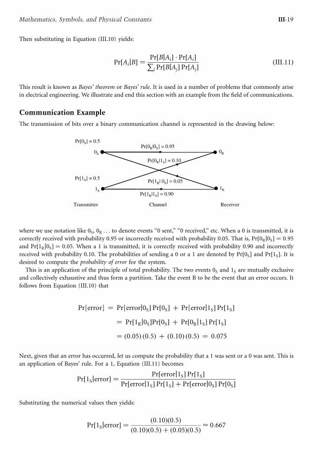
Then substituting in Equation (III.10) yields:
Pr½AijB ¼ Pr½BjAi · Pr½AiPj Pr½BjAj Pr½Aj ðIII:11Þ
This result is known as Bayes’ theorem or Bayes’ rule. It is used in a number of problems that commonly arise
in electrical engineering. We illustrate and end this section with an example from the field of communications.
Communication Example
The transmission of bits over a binary communication channel is represented in the drawing below:
Pr[0R|0S] = 0.950S 0R
1RPr[1R|1S] = 0.90
Pr[1R| 0S] = 0.05
Pr[0R|1S] = 0.10
Pr[0S] = 0.5
Pr[1S] = 0.5
1S
Transmitter Channel Receiver
where we use notation like 0S, 0R . . . to denote events ‘‘0 sent,’’ ‘‘0 received,’’ etc. When a 0 is transmitted, it is
correctly received with probability 0.95 or incorrectly received with probability 0.05. That is, Pr½0Rj0S ¼ 0:95
and Pr½1Rj0S ¼ 0:05. When a 1 is transmitted, it is correctly received with probability 0.90 and incorrectly
received with probability 0.10. The probabilities of sending a 0 or a 1 are denoted by Pr½0S and Pr½1S . It isdesired to compute the probability of error for the system.
This is an application of the principle of total probability. The two events 0S and 1S are mutually exclusive
and collectively exhaustive and thus form a partition. Take the event B to be the event that an error occurs. It
follows from Equation (III.10) that
Pr[error] ¼ Pr[errorj0S Pr½0S þ Pr[errorj1S Pr½1S¼ Pr½1Rj0S Pr½0S þ Pr½0Rj1S Pr½1S¼ ð0:05Þ ð0:5Þ þ ð0:10Þ ð0:5Þ ¼ 0:075
Next, given that an error has occurred, let us compute the probability that a 1 was sent or a 0 was sent. This is
an application of Bayes’ rule. For a 1, Equation (III.11) becomes
Pr½1Sjerror ¼ Pr½errorj1S Pr½1SPr½errorj1S Pr½1S þ Pr½errorj0S Pr½0S
Substituting the numerical values then yields:
Pr½1Sjerror ¼ ð0:10Þð0:5Þð0:10Þð0:5Þ þ ð0:05Þð0:5Þ < 0:667
III-19Mathematics, Symbols, and Physical Constants

For a 0, a similar analysis applies:
Pr½0Sjerror ¼ Pr½errorj0S Pr½0SPr½errorj1S Pr½1S þ Pr½errorj0S Pr½0S
¼ ð0:05Þð0:5Þð0:10Þð0:5Þ þ ð0:05Þð0:5Þ < 0:333
The two resulting probabilities sum to 1 because 0S and 1S form a partition for the experiment.
Reference
1. C. W. Therrien and M. Tummala, Probability for Electrical and Computer Engineers. Boca Raton, FL:
CRC Press, 2004.
III-20 Mathematics, Symbols, and Physical Constants

Indexes
Author Index ........................................................................................................................................................ A-1
Subject Index ........................................................................................................................................................ S-1


Author Index
A
Arif, Ronald, Semiconductor Nano-
Electroncis and Nano-
Optoelectronics, Materials and
Nanoscience, 4-68 to 4-89
B
Barnes, Frank, Biological Effects and
Electromagnetic Fields,
Bioelectricity, 7-33 to 7-54
Barr, R. C., Bioelectric Events,
Bioelectricity, 7-13 to 7-33
Berbari, Edward J., The
Electrocardiograph,
Bioelectronics and Instruments,
9-14 to 9-21
Bond, Robert A., Embedded Signal
Processing, Bioelectricity,
7-55 to 7-75
Bronzino, Joseph D., The Electro-
encephalogram, Bioelectronics
and Instruments, 9-1
to 9-13
D
Dhillon, B. S., Reliability Engineering, 6-1
to 6-19
Dorval II, Alan D., Neuroelectric
Principles, Bioelectricity, 7-1 to
7-12
E
Eren, Halit, Portable Instruments
and Systems, Instruments
and Measurements, 5-27
to 5-35
F
Fox, Martin D., Tomography, 10-1 to
10-7
G
Geddes, L. A., Bioelectric Events,
Bioelectricity, 7-13 to 7-33
Giurgiutiu, Victor, Micromechatronics,
Materials and Nanoscience, 4-20
to 4-42
H
Hall, David L., An Introduction to Multi-
Sensor Data Fusion, 2-1
to 2-14
Hobbs, Bryan Stewart, Electrochemical
Sensors, Sensors, 1-11 to 1-17
J
Jin, Zhian, Semiconductor Nano-
Electroncis and Nano-
Optoelectronics, Materials and
Nanoscience, 4-68 to 4-89
K
Khalilieh, Sam S., Electrical Equipment in
Hazardous Areas, Instruments
and Measurements, 5-1 to 5-27
L
Llinas, James, An Introduction to Multi-
Sensor Data Fusion, 2-1
to 2-14
Lyshevski, Sergey Edward
Micromechatronics, Materials
and Nanoscience, 4-20
to 4-42
Nanocomputers, Nano-Architectronics,
and Nano-ICs, Materials and
Nanoscience, 4-42 to 4-68
M
Martinez, David R., Embedded Signal
Processing, Bioelectricity, 7-55 to
7-75
Meyyappan, M., Carbon Nanotubes,
Materials and Nanoscience, 4-1
to 4-8
N
Neuman, Michael R., Biomedical Sensors,
8-1 to 8-12
P
Pelasko, John, Modeling MEMS and
NEMS, Materials and
Nanoscience, 4-9 to 4-20
Pu, Yuan, Magneto-optics, 3-1 to 3-10
R
Relf, Christopher G., G (LabVIEW2)
Software Engineering,
Instruments and Measurements,
5-36 to 5-54
S
Slaten, Bonnie Keillor, Biological Effects
and Electromagnetic Fields,
Bioelectricity, 7-33
to 7-54
A-1

Smith, Rosemary L., Introduction,
Sensors, 1-1 to 1-10
T
Tallarida, Ronald J., Mathematics,
Symbols, and Physical Constants,
III-1 to III-20
Tansu, Nelson, Semiconductor
Nano-Electroncis and Nano-
Optoelectronics, Materials
and Nanoscience, 4-68 to 4-89
Therrien, Charles W., Probability
for Electrical and Computer
Engineers, Mathematics,
Symbols, and Physical
Constants, III-14 to III-20
V
Vai, M. Michael, Embedded Signal
Processing, Bioelectricity, 7-55 to
7-75
W
Watson, Joseph, The Stannic Oxide
Semiconductor Gas Sensor,
Sensors, 1-18 to 1-24
White, John A., Neuroelectric Principles,
Bioelectricity, 7-1 to 7-12
Y
Young, David, Magneto-optics, 3-1 to
3-10
A-2 Sensors, Nanoscience, Biomedical Engineering, and Instruments

Subject Index
A
Action potential, 7-1, 7-11; see also
Neuroelectric principles
Activating function, 7-11
Activation, 7-11
Air current and ventilation, 5-4
Amperometric sensor, 8-10
Analyte, 8-10
Atrophy, 7-32
Autonomic, 7-32
Availability, 6-2
B
Babbage, Charles, 4-44
Bioanalytical sensors, 8-2, 8-10; see also
Biosensors
Bioelectric events, 7-13, 7-31 to 7-32
electro-encephalography (EEG), 7-23
to 7-24
clinical EEG, 7-26 to 7-27
evoked potentials, 7-27 to 7-29
instrumentation, 7-27
normal EEG, 7-25 to 7-26
recording technique, 7-24
to 7-25
electrocardiogram (ECG)
clinical signal, 7-17 to 7-19
ECG leads, 7-19
instrumentation, 7-19 to 7-720
origin, 7-15 to 7-17
recordings taken directly from the
heart, 7-21
electrograms, 7-21
electromyography (EMG), 7-21
clinical EMG, 7-22 to 7-23
contraction of skeletal muscle, 7-21
to 7-22
instrumentation, 7-23
law of stimulation, 7-14
magnetic (Eddy-Current) stimulation,
7-29 to 7-30
recording action potentials, 7-14 to
7-15
terminology, 7-32
Bioelectrical nanocomputers, 4-43 to
4-44
Bioelectricity, origins, 7-13 to 7-14; see
also Bioelectric events;
Biological effects and
electromagnetic fields;
Embedded signal processing;
Neuroelectric principles
Bioelectronics and instruments. See
Electrocardiograph;
Electro-encephalogram
Biological effects and electromagnetic
fields, 7-33, 7-52
biological effects of electric shock,
7-34, 7-34
electromagnetic fields from cell
phones and base stations, 7-41
animal studies (in vivo), 7-44 to
7-45
cellular studies, 7-45 to 7-46
epidemiological studies, 7-42 to
7-43
exposures, 7-42
low-level/time-varying
electromagnetic fields from
power lines, 7-36
animal studies, 7-38 to 7-40
cellular studies, 7-40 to 7-41
epidemiological studies, 7-37 to
7-38
exposures, 7-36 to 7-37
other adverse effects of electricity,
electrical arc flash, 7-36
risk, 7-50 to 7-52
shock from household voltage, 7-35
standards/guidelines, 7-46 to 7-48
Biomedical sensors, 8-1 to 8-2, 8-10,
8-11
applications, 8-10
bioanalytical sensors, 8-9 to 8-10
chemical sensors, 8-6 to 8-9
physical sensors, 8-2 to 8-6
Biosensors, 1-7, 8-2
enzyme sensor, 1-8
immunosensor, 1-7 to 1-8
Bispectra, 9-13
Block (wiring) diagram, 5-53
‘‘Buckeyball structure’’, 4-17
C
Carbon nanotubes (CNTs), 4-1, 4-8
atomic force microscopy (AFT) and
CNT probes, 4-6 to 4-7
field emission, 4-8
growth, 4-2 to 4-5
arc synthesis, 4-2 to 4-3
CVD (chemical vapor deposition),
4-3
PECVD (plasma enhanced CVD),
4-3
plasma sources, 4-4
nano-electronics, 4-5 to 4-6
sensors, 4-7 to 4-8
structure and properties, 4-2
Page on which a term is defined is indicated in bold.
S-1

Chemical sensors, 1-5 to 1-6, 8-11
gas chromatograph, 1-7
ion-selective electrode (ISE), 1-6 to
1-7
Chronaxie, 7-11
CMOS (complementary metal oxide
semiconductor), 4-25
CMOS transistors, 4-55
Combustible liquids, 5-3
Compton, Arthur H., scattering
experiment, 4-70
Constituitive relation, 4-18
Continuum hypothesis, 4-12, 4-18
Continuum mechanics, 4-18
Conversion constants and multipliers,
III-6 to III-7
Cotton—Mouton effect/magnetic
linear birefringence, 3-3 to 3-4,
3-10
Coulomb blockade, 4-79
Coupled domain problem, 4-18
Cross spectra, 9-13
Current clamp, 7-11
D
Dasarathy’s Functional Model (data
fusion process model), 2-11
Data fusion; see also Multi-sensor data
fusion
applications, 2-5
condition-based monitoring (CBM)
of complex systems, 2-6
environmental monitoring, 2-6
medical applications, 2-7
military applications, 2-7
nondestructive evaluation (NDE),
2-7
limitations of systems, to 2-13, 2-12
process models, 2-7 to 2-8
Bedworth and O’Brien’s Omnibus
Model, 2-11
Boyd’s Decision Loop Model,
2-11
Dasarathy’s Functional Model,
2-11
Joint Directors of Laboratories
(JDL) model, 2-8 to 2-11
similarities to human cognitive
processes, 2-1 to 2-2
techniques, 2-3
a priori knowledge about input
data/estimation processes, 2-5
data fusion architecture, 2-5
decision level fusion, 2-3
nature/heterogeneity of input data,
2-3, 2-5
Data type, 5-53
de Broglie’s hypothesis, 4-70 to 4-71
Decision Loop Model (Boyd), 2-11
Dynamic clamp, 7-11
E
ECG lead, 9-20
Ectopic beat, 7-32
Electrical equipment/hazardous areas,
5-1; see also Explosion
protection
certification and approval, 5-17 to
5-19
enclosure types/requirements, 5-10
equipment use and hierarchy, 5-26 to
5-27
hazardous areas classification, 5-4 to
5-5
hazardous areas classification/
methods, 5-5
hazardous areas division classification
(NEC method), 5-6 to 5-7
ignition curves, 5-14 to 5-17
IS ground rules, 5-20
combustible gas detection system,
5-25 to 5-26
dust-ignition proof, 5-20 to 5-22
encapsulation, 5-24 to 5-25
explosion proof design, 5-20
hermetically sealed, 5-25
increased safety, 5-25
non sparking (nonincendive), 5-24
nonincendive circuit, 5-24
nonincendive component, 5-24
oil immersion, 5-24
powder filled, 5-23 to 5-24
purging and pressurization
methodology, 5-22 to 5-23
making field devices intrinsically safe,
5-13 to 5-14
protection methodologies, 5-11
intrinsic safety (IS), 5-11 to 5-13
terminology, 5-3 to 5-4, 5-27
zone classification, 5-7 to 5-10
Electro-encephalogram (EEG), 9-1, 9-13
frequency analysis, 9-6 to 9-8
historical perspective, 9-3 to 9-4
language of the brain, 9-1 to 9-3
nonlinear analysis, 9-8 to 9-10
recording techniques, 9-4 to 9-6
topographic mapping, 9-10 to 9-12
Electrocardiograph (ECG), 9-14 to 9-16,
9-20
instrumentation, 9-17 to 9-20
physiology, 9-17
Electrochemical sensors
advantages, 1-11
amperometric sensors, 1-13, 1-15 to
1-17
potentiomatic sensors, 1-11 to 1-12
Electron tunneling, 4-78
Embedded digital signal processor
(DSP), 7-60
programmable
advantages of, 7-60 to 7-61
challenges of, 7-61 to 7-62
DSP hardware, 7-62 to 7-65
benchmarking, 7-66
technology trends, 7-69 to 7-70
software/runtime and development
environment, 7-67 to 7-69
Embedded signal processing, 7-55 to
7-56, 7-55, 7-75
active electronically steered array
(AESA)-based sensor systems,
7-55
application-specific hardware, 7-70 to
7-71
FPGA (field programmable gate
arrays) design, 7-73 to 7-74
full-custom ASIC
(application-specific integrated
circuits), 7-72 to 7-73
intellectual property (IP) core
approach, 7-74 to 7-75
and semiconductor technology,
7-71 to 7-72
standard-cell ASIC
(application-specific integrated
circuits), 7-73
structured ASIC, 7-74
generic architecture, 7-56 to 7-60
Error cluster, 5-54
Explosion protection
avoidance techniques, 5-2 to 5-3
basic reaction, 5-2
hazardous area terminology, 5-3 to 5-4
F
Failure, 6-2
Farraday rotation/magnetic circular
birefringence, 3-2 to 3-3, 3-10
Fast Fourier transform (FFT), 9-13
Feynman, Richard, 4-9
Flammable limits (FL), 5-3
Flammable liquids, 5-3
Flash point (FP), 5-3
Front panel, 5-54
Fuels, 5-4
G
G, 5-54; see also LabVIEW development
system
Gas sensors, ‘‘solid state’’, 1-18; see also
Stannic oxide semiconductor
gas sensor
Greek alphabet, III-3
Ground, 5-27
H
Hazard rate, 6-2
Heat equation, 4-18
HRECG, 9-20
S-2 Sensors, Nanoscience, Biomedical Engineering, and Instruments

Human error, 6-2
Hypocapnia, 7-32
Hypoxia, 7-32
I
Ignition temperature, 5-3
Inactivation, 7-12
Inductance, 5-27
Installer, 5-54
Intel Pentium processor/Microburst
microarchitecture, 4-44
International Electrotechnical
Commission (IEC)/Zone
Classification method, 5-5
International System of Units (SI)
definitions, III-3 to III-4
names and symbols for SI base units,
III-4
SI derived units with special names
and symbols, III-4 to III-5
units in use with SI, III-5
J
Joint Directors of Laboratories (JDL)
model, 2-8 to 2-11
K
Kerr effects, 3-4 to 3-5, 3-10
L
LabVIEW development system, 5-36,
5-54
application building (creating
executables), 5-50
installers, 5-52
reverse engineering built
executables, 5-51
runtime engine (RTE), 5-51
runtime licenses (RTLs), 5-51 to
5-52
code distribution, 5-48
application distribution library,
5-49
development distribution library,
5-49
diagram access, 550t, 5-49 to 5-50
VI library ( .llb), 5-49
data coerceion, 5-40 to 5-41
data types, 5-36 to 5-37
error handling, 5-41
custom error codes, 5-44 to 5-46
default error codes, 5-44
error cluster, 5-41
usage, 5-41 to 5-43
wiring errors/subVI connector
pane, 5-43
G programming language, 5-36, 5-54
GOOP (graphical object-oriented
programming), 5-47 to 5-49
open source G/distributed
development, 5-52 to 5-53
polymorphism, 5-38 to 5-39
shortcuts, 5-47
front panel and block diagram,
5-47
keyboard, 5-46
tool palette, 5-46 to 5-47
terminology, 5-53 to 5-54
units, 5-39 to 5-40
LIGA/LIGA-like high-aspect-ratio,
4-25
Ligand-gated ion channels, 7-12
Linear thermoelasticity, 4-18
Lower explosive limit (LEL), 5-3
Lower flammable limit (LFL), 5-3
M
Magnetic stimulation, 7-32
Magneto-optics, 3-1 to 3-2
applications
magneto-optic recording, 3-9 to
3-10, 3-10
MSW-based guided-wave
magneto-optic Bragg cell, 3-8 to
3-9, 3-10
optical isolator and circulator, 3-5
to 3-8, 3-10
classification of effects
Cotton—Mouton effect/magnetic
linear birefringence, 3-3 to 3-4
Farraday rotation/magnetic circular
birefringence, 3-2 to 3-3
Kerr effects, 3-4 to 3-5
Magnitude squared coherence (MSC),
9-13
Mathematical modeling, 4-10, 4-18
Mathematics, III-1 to III-2; see also
Symbols and physical constants
Maximum surface temperature, 5-3
Maxwell’s equations, 4-18
Mean time to failure (exponential
distribution), 6-2
Measuring instruments, 5-27
Measuring instruments (portable),
5-35
applications, 5-33 to 5-35
communicating and networking of,
5-31 to 5-32
digital portable instruments, 5-29 to
5-30
features, 5-28
main groups, 5-28
power requirements, 5-28 to 5-29
sensor for, 5-30 to 5-31
wireless portable instruments and
networks, 5-32 to 5-33
Membrane potential, 7-12
MEMS and NEMS modeling, 4-9, 4-18,
4-19
approaches, 4-12
continuum mechanics, 4-12
to 4-17
coupled domains, 4-17
history of, 4-9 to 4-10
other tools, 4-17 to 4-18
‘‘Buckeyball structure’’, 4-17
self-assembly, 4-17 to 4-18
and resonant gate transistor
development, 4-10
science of scale, 4-10 to 4-12
self-assembly (SA) and
self-organization (SO) study,
4-18
Metabolic process, 7-32
Micro-electrical modeling systems
(MEMS). SeeMEMS and NEMS
modeling
Micromatching, 1-8 to 1-9, 1-10
Micromechatronics, 4-20; see also
Piezoelectric wafer active
sensors (PWAS)
electroactive and magnetoactive
materials, 4-26
electroactive materials, 4-26 to 4-27
magnetoactive materials, 4-27 to
4-28
fabrication aspects, 4-25 to 4-26
induced-strain actuators, 4-28
design with, 4-20
linearized electromechanical behavior
of induced-strain actuators,
4-29 to 4-31
microcontrollers sensing/actuation/
process control, 4-40 to 4-42
synchronous micromachines, 4-22 to
4-25
systems introduction, 4-20 to 4-21
Microsensors, 1-8 to 1-9
Molecular dynamics, 4-18
Moore’s laws, 4-44
Multi-sensor data fusion, 2-1 to 2-2,
2-13 to 2-14; see also Data
fusion
Muscular dystrophy, 7-23
Myasthenia gravis, 7-23
Myocardial infarction, 7-32
Myotonia, 7-23
N
Nano-architectronics. See
Nanocomputers/
nano-architectronics/nano-ICs
Nano-electromechanical modeling
systems (NEMS). See MEMS
and NEMS modeling
Nano-ICs. See Nanocomputers/
nano-architectronics/nano-ICs
S-3Subject Index

Nanocompensator synthesis and design
aspects, 4-66 to 4-67
Nanocomputers/nano-architectronics/
nano-ICs, 4-42 to 4-44
applied and experimental results,
4-43
architecture (nanocomputers), 4-54 to
4-59
benchmarking opportunities, 4-42 to
4-43
classification of nanocomputers,
4-47
fundamentals (nanoelectronics and
nanocomputers), 4-45 to 4-54
memory management, 4-46
memory—processor interface, 4-48
to 4-50
multiprocessors, 4-51 to 4-52
nanocomputer architectronics, 4-52
to 4-53
parallel memories, 4-50 to 4-51
pipelining, 4-51
processor and memory hierarchy,
4-47
two-/three-dimensional topology
aggregation, 4-53 to 4-54
hierarchical finite-state machines/use
in hardware and software
design, 4-59 to 4-63
steps in heuristic synthesis, 4-60
mathematical models
(nanocomputers)
with parameters set, 4-66
sixtuple nanocomputer model, 4-65
and Moore’s laws, 4-44
nanocompensator synthesis and
design aspects, 4-66 to 4-67
reconfigurable nanocomputers, 4-63
to 4-65
three-dimensional nano-ICs, 4-44
types of nanocomputers, 4-43
bioelectrical, 4-43 to 4-44
mechanical, 4-44
reversible/irreversible, 4-45
Nanoscience materials. See Carbon
nanotubes; MEMS and NEMS
modeling; Micromechatronics;
Nanocomputers,
nano-architectronics, and
nano-ICs; Semiconductor
nano-electronics and
nano-optoelectronics
Navier equations, 4-18
Navier—Stokes equations, 4-18
NEC Division Classification method,
5-5
Nernst potential, 1-6
Neuroelectric principles, 7-1 to 7-2
action potentials, 7-1, 7-3 to 7-6
application/deep brain stimulation,
7-10 to 7-11
dynamic clamp, 7-6 to 7-8
electrochemical potential, 7-2
to 7-3
extracellular stimulation models, 7-8
to 7-10
activating function, 7-8
chronaxie, 7-8
rheobase, 7-8
synaptic transmission, 7-6
Noninvasive sensor, 8-11
Normal Operation, 5-27
O
Occipital, 7-32
Omnibus Model (Bedworth and
O’Brien), 2-11
Optical fiber telecommunications
applications. See Semiconductor
nano-optoelectronics
Oxidation, 5-27
P
Parietal, 7-32
Pellistor sensor, 1-18
pH glass electrode, 1-6
Physical constants. See Symbols and
physical constants
Physical sensor, 8-11
Physical sensors, 1-2, 1-4
displacement and force, 1-5
optical radiation, 1-5
temperature, 1-4
Piezoelectric wafer active sensors
(PWAS), 4-32
PWAS modal sensor and
electromechanical impedance
method, 4-38 to 4-40
PWAS phased array, 4-37 to 4-38
PWAS resonators, 4-32
circular, 4-33 to 4-34
rectangular, 4-32 to 4-33
PWAS transmitters and receivers of
elastic waves, 4-34, 4-36
Piezoresistor, 1-2
Planck’s Law, 4-69
Pn-junction photodiode, 1-5
Polymorphic virtual instruments (VIs),
5-38, 5-54
Portable instruments. See Measuring
instruments (portable)
Potentiomatic sensors, 1-11
to 1-12
Potentiometric sensor, 8-11
Potentiometric measurement, 8-8
Power spectral analysis, 9-13
Q
Quadratic phase coupling, 9-13
R
Random failure, 6-2
Redundancy, 6-2
Refractory period, 7-12
Reliability, 6-2
Reliability engineering, 6-1
bathtub hazard-rate concept, 6-2 to
6-3
formulas, 6-3 to 6-5
human reliability, 6-13
classification and causes of human
errors, 6-13
measures, 6-13 to 6-14
modeling human operation in a
fluctuating environment, 6-14
to 6-16
reliability evaluation methods, 6-8
failure modes and effect analysis,
6-8 to 6-9
fault-tree analysis, 6-9
Markov method, 6-11 to 6-13
probability evaluation, 6-10 to 6-11
reliability networks, 6-5
k-out-of-m network, 6-7 to 6-8
parallel network, 6-6 to 6-7
series network, 6-5 to 6-6
robot reliability, 6-16
measures, 6-16 to 6-18
robot failure classification and
causes, 6-16
terms/definitions, 6-2
Reliability formula, 6-3
Repair rate, 6-2
Repeatability, 1-10
Resistance thermometer, 1-4
Resonant gate transistor development,
4-10
RTD, 5-27
Runtime engine (RTE), 5-54
Runtime license (RTL), 5-54
S
Seebeck effect, 1-4
Self-assembly, 4-19
Semiconductor nano-optoelectronics
gain media for telecom lasers/
InGaAsN and InAs QDs, 4-85 to
4-86
implementation/epitaxy of gain media
into devices, 4-82
quantum dots lasers, 4-84
quantum-effects based gain media/
laser applications, 4, 80 to 4-82
quantum intersubband lasers, 4-87 to
4-88
strained quantum well lasers, 4-83 to
4-84
Type-II quantum well lasers, 4-86 to
4-87
S-4 Sensors, Nanoscience, Biomedical Engineering, and Instruments

Semiconductor nanoelectronics/resonant
tunneling diode
application, 4-77 to 4-78
nanoelectronics and tunneling
phenomenon, 4-72 to 4-73
particle tunneling through a potential
barrier, 4-75
quantum tunneling phenomenon,
4-73 to 4-74
resonant tunneling—double barrier
potential, 4-75 to 4-77
Semiconductor nanotechnology, 4-68 to
4-69
fundamental physics of/quantum
physics
duality of particle and wave/
electron as a wave, 4-70 to 4-71
duality of particle and wave/light as
a particle, 4-69 to 4-70
and quantum effects, 4-71 to 4-72
future directions, 4-88 to 4-89
Semiconductor nanoelectronics/single
electron transistors
operation, 4-80
theoretical basis, 4-78 to 4-79
Sensitivity, 1-10
Sensors, 1-1, 1-10; See also Biosensors;
Chemical sensors;
Electrochemical sensors;
Multi-sensor data fusion;
Physical sensors; Stannic oxide
semiconductor gas sensor
block diagram, 1-1 to 1-2
demand for, 1-1
direct/indirect, 1-1
factors in choice for applications, 1-2
SET. See Semiconductor nanoelectronics/
single electron transistors
Space clamp, 7-12
Stability, 1-10
Stannic oxide semiconductor gas sensor,
1-18
basic electric parameters and
operation, 1-18 to 1-20
electrical operating parameters, 1-23
future directions, 1-23
operating temperature, 1-21
substrate materials, 1-22
Steady-state condition (statistical), 6-2
Strain gage, 1-5
Surface micromachining technologies,
4-25
Symbols and physical constants; See also
Conversion constants and
multipliers; International
System of Units (SI)
Greek alphabet, III-3
physical constants, III-8 to III-9
T
Thermistors, 1-4
Thermocouple, 1-4
Tomography, 10-1, 10-7
computerized, 10-1 to 10-3
axial tomography (CAT/CATscan),
10-1, 10-6
tomography (CT), 10-1
imaging, 10-5 to 10-6
magnetic resonance imaging (MRI),
10-1, 10-4 to 10-5, 10-6
positron emission tomography (PET),
10-1, 10-3 to 10-4, 10-7
single photon emission computed
tomography (SPECT), 10-1,
10-4, 10-7
Transducer, 1-1
auto-generators, 1-2
mechanisms, 1-2
modulators, 1-2
Twelve-lead ECG, 9-20
U
Unit, 5-54
Upper explosive limit (UEL), 5-3
V
Vapor density, 5-3
Vapor dispersion, 5-4
Voltage clamp, 7-12
Voltage-gated ion channels, 7-12
W
Wilson central terminal, 9-20
Z
Zener diode, 5-27
S-5Subject Index


TAYLOR & FRANCIS
www.tandf.co.uk/journals
Nanotoxicology
Editor: Prof.C.Vyvyan Howard, University of Liverpool, UK
Email: [email protected]
Print ISSN 1743-5390
Online ISSN 1743-5404
Nanotoxicology invites contributions
addressing research into the interactions
between nano-structured materials and living
matter. Although much of the activity of the
Journal involves the investigations of the biological
interactions with nano-scale materials, its scope
extends to include all man-made
nano-structured materials.
The nature of the interactions within the scope of the journal includes the mobility,
persistence and toxicity of nano-structured materials and their breakdown products in
humans, experimental animals, the environment and within biota. Developments in
technique for assessing and measuring such interactions through the use of in vitro and
in vivo methods for risk assessments are a major area of interest. The Journal is
particularly interested in methods of toxicity minimisation in fields such as the medical
and therapeutic use of nano-particles in the treatment of disease. Within its scope, the
Journal also includes evidence of harm from
nano-structured materials.
Nanotoxicology is published WebFirst (www.tandf.co.uk/webfirst) – comprising of four
online issues and an end of year print archive volume, allowing accelerated publication
times and providing faster access to key peer-reviewed research.
Visit www.nanotoxicology.net for further information.
NEW JOURNAL
For further information or to subscribe please contact Louise Porter at the following address:
Taylor & Francis, 4 Park Square, Milton Park, Abingdon, OXON, OX14 4RN, UKEmail: [email protected] Fax: +44 (0)20 7017 6714
Register your email address at www.tandf.co.uk/eupdates to receive information on
books, journals and other news within your areas of interest.
SARA is a free email contents alerting service designed to deliver tables of contents
for over 1050 journals of your choice in advance of the printed edition. Registering
for the service is simple and you can now request to receive alerts by keyword or by
title. For more information visit www.tandf.co.uk/sara