Embed Size (px)
Citation preview
575
27Sensor Signal Conditioning for Biomedical Instrumentation
Tomas E. Ward
27.1 Introduction
Many connected health applications as with telemedical systems rely on the acquisition and transmission of physiological measurement in a reliable and robust fashion. This is achieved by sensor front ends, which are increasingly found in both wearable and ambi-ent forms. These embodiments require nonintrusive, low-power, safe, and reliable opera-tion in the face of activities of daily living, which place the technology in environments well outside the regulated conditions of the research laboratory (Sweeney et al., 2012a). Furthermore, as digital communication systems provide ever-improving performance
CONTENTS
27.1 Introduction ........................................................................................................................ 57527.2 Sensors ................................................................................................................................. 57727.3 Signal Conditioning........................................................................................................... 578
27.3.1 The Operational Amplifier ................................................................................... 57827.3.2 Signal Amplification with Operational Amplifiers .......................................... 579
27.3.2.1 Example: Piezoelectric Transducer Compensation ............................58327.3.3 The Instrumentation Amplifier ...........................................................................585
27.4 The Analog-to-Digital Conversion Process .................................................................... 58927.4.1 The Sampling Process ........................................................................................... 59027.4.2 The Quantization Process ..................................................................................... 59127.4.3 Antialiasing Filters ................................................................................................ 59227.4.4 Oversampling and Decimation ........................................................................... 597
27.4.4.1 Oversampling .......................................................................................... 59727.4.4.2 Multisampling ......................................................................................... 597
27.5 Integrated Solutions........................................................................................................... 59827.6 Isolation Circuits ................................................................................................................600
27.6.1 Methods of Isolation ..............................................................................................60027.6.1.1 Capacitive Isolation Amplifiers .............................................................60027.6.1.2 Optical Isolation Amplifiers ..................................................................60027.6.1.3 Magnetic Isolation Amplifiers ............................................................... 60227.6.1.4 Digital Isolation ....................................................................................... 602
27.7 Conclusions ......................................................................................................................... 602References .....................................................................................................................................603
© 2016 by Taylor & Francis Group, LLC
576 Telehealth and Mobile Health
in terms of information rate, reliability, power consumption, and physical size, there is increasing emphasis on the sensor and sensor-side processing to deliver high-fidelity rep-resentations of the measurand under consideration. Taken together, these push demand toward ever more sophisticated sensor processing yet in physical forms which are smaller, faster, and cheaper. Computational approaches to sensor output processing, especially with respect to the processing of physiological artifacts, are driving the modern tendency toward capturing the output of the sensor in digital form as early as possible in the signal pipeline. In this scenario, only essential filtering and preprocessing steps are performed in the analog domain. Notwithstanding this tendency, there is considerable scope to con-dition the sensor output to contribute significantly to the overall pipeline signal-to-noise ratio (SNR) figure. It is tempting, due to the ever-increasing capability of modern compu-tational methods to clean up a noise-corrupted sensor signal, to be complacent in regard to noise reduction at the sensor side but it is important to note that there is no substi-tute for good-quality, clean data (Kappenman and Luck, 2013). The introduction of noise occurs easily and through many mechanisms—removing it is always difficult so it is best to minimize its introduction in the first place (Webster, 1998). Appropriate shielding, sen-sor design, wiring, and grounding practice has very significant impact in terms of reduc-ing noise onto the sensor reading, while judicial use of basic filtering and amplification can subsequently improve the SNR at an early stage (Metting van Rijn et al., 1990). The level of acceptable signal-to-noise ratio on a sensor reading is application specific; therefore, the SNR over the complete sensor-processing pipeline must be considered during design to develop an appropriate approach in line with the engineering constraints.
For example, single-trial event-related potential (ERP) measurement via noninvasive EEG for the purposes of brain–computer interfacing presents very poor SNR, and conse-quently, analog design engineers use considerable ingenuity in devising circuitry which can deliver an acceptable SNR for subsequent ERP interpretation (Metting van Rijn et al., 1990, 1991). In contrast, the use of a thermistor as a sensor as part of a system for mea-suring respiratory rate (such a thermistor is placed near the nostrils and/or integrated into a breathing mask) is characterized by robust SNR and only relatively simple circuit techniques are required to produce a signal suitable for basic respiratory rate analysis (Bronzino, 1995).
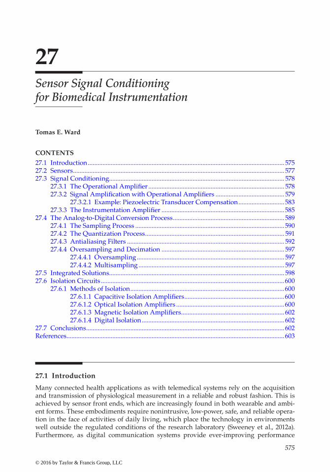
Regardless of the precise nature of the application or sensor modality, an abstraction of the sensor-side processing stages is easily to visualize. The canonical signal-processing pipeline under consideration in this chapter is illustrated in Figure 27.1. Such a pipeline serves the purpose of optimizing SNR for data acquisition and subsequent processing for
Excitationcircuit
Sensor Antialiasingfilter
Communications
Analog-to-digitalconversion
Analogconditioning
FIGURE 27.1High-level view of the sensor-processing pipeline.
© 2016 by Taylor & Francis Group, LLC
Dow
nloa
ded
by [
Tom
as W
ard]
at 0
9:59
10
Dec
embe
r 20
15
577Sensor Signal Conditioning for Biomedical Instrumentation
a specific application. It is worth remarking that if there are potentially many applications that may require the output of this particular sensor, then the SNR budget (end-to-end) needs to be considered for the most demanding case.
The purpose of this chapter then is to highlight the signal-conditioning components in Figure 27.1, including some practical advice on implementation. This signal-conditioning pipeline can range from the very simple—such as a signal buffer—to very complex ana-log systems. In this chapter, we give a concise overview of the possibilities with an emphasis on basic analog building blocks that can then be used to construct the range of processing functions most commonly encountered. We start on the left-hand side with a short introduction to sensors before traversing the various stages that comprise the pipeline.
27.2 Sensors
A sensor is a device that measures a physical quantity and converts it into a form that can ultimately be interpreted by an observer. It is natural to think of the observer as a person but it can just as easily be any subsequent system whose state is influenced by the sensor output—any measurement instrument can be interpreted in this way—so too are more complex systems, including software systems—from agents to expert systems which rely on sensor output to produce useful output. Most sensors act as transducers; i.e., energy is converted from one form into another. For the purposes of connected health applications as discussed in this chapter, whatever the physical quantity of interest is, it must ulti-mately be converted into an electrical form of energy and, more specifically, it is desired that changes in the physical quantity are mapped onto changes in voltage as commodity digitization systems (analog-to-digital convertors) are overwhelmingly voltage-based. For some sensors, this conversion to electrical forms of energy is inherent to the physics of the sensing phenomenon (e.g., the use of electrodes to measure electrical activity in the body); while for others, subsequent processing, usually within the sensor package, is required to produce this conversion effectively. As an example of the latter, a digital stethoscope requires an appropriate sensor to convert acoustic energy into an electrical signal. Such a sensor comprises a diaphragm that provides the acoustic amplification and which, in the past, constituted the sensor because an observer—in this case, a person—could now listen to the suitably amplified sound either directly or through an acoustic tube attached to the ear (the classic stethoscope). A digital stethoscope augments the sensing compo-nent through the addition of a transducer that converts the acoustic energy to electrical energy—the transducer is typically, in this case, a condenser microphone that converts acoustic energy through changes in capacitance to changes in voltage. This voltage signal can be digitized and stored electronically and used for interpretation either directly by a human expert or is subsequently processed as part of a more sophisticated system; e.g., acoustic signals of a cardiac origin can be analyzed automatically for specific abnormal patterns (Wang et al., 2009). While it is important to appreciate the fundamental aspects of sensing as discussed above, it should be noted that modern sensors are designed and packaged such that their output is amenable for processing directly with electrical circuits and increasingly directly with digital systems (Fraden, 2010). We do not consider the latter in this chapter and will instead focus on sensors that produce an analog voltage that can be directly related to the measurand under consideration.
© 2016 by Taylor & Francis Group, LLC
Dow
nloa
ded
by [
Tom
as W
ard]
at 0
9:59
10
Dec
embe
r 20
15
578 Telehealth and Mobile Health
Sensors for physiological measurement come in many shapes, sizes, types, and configu-rations. There are journals and texts devoted to the topic and it is a continuously active focus of research and development, especially in the healthcare domain. In the realm of health, the most common measurements of interest relate to the primary vital signs—temperature, blood pressure, pulse, respiratory rate along with electrical activities of the heart and of the brain, and arterial oxygenation saturation levels (Humphreys et al., 2007). Many of the above measurements are obtained using self-contained systems complete with digital output and, increasingly, web connectivity (Carlos et al., 2011). For the purposes of this chapter, we will focus our attention on sensor systems that require further analog processing such as bespoke EEG, EMG, ECG, and biophotonic sensor systems. Returning now to the basic sensor-processing pipeline as illustrated in Figure 27.1, we next examine the signal-conditioning stage. This stage is the primary focus of this chapter and consider-able attention will be devoted to approaches commonly used here.
27.3 Signal Conditioning
In the context of sensors, signal conditioning refers to the process by which the output of the sensor package, which as discussed earlier will be assumed to be a voltage sig-nal, is subsequently processed to enhance its utility for the intended application. For many applications of sensors, this stage is concerned with enhancing SNR—this is the utilitarian function required from the signal-conditioning stage and is achieved primar-ily through amplification and filtering. More sophisticated processing such as feature extraction can also be carried out here, but the contemporary approach is to reserve these processing steps for the digital domain and, more specifically, for software-driven pro-cessing routines.
The analog circuitry in modern data-acquisition systems is consequently concerned with amplification and the systems used are built using the basic analog amplifier build-ing block—the operational amplifier (op-amp). In this chapter, we will highlight the utility and versatility of the operational amplifier in this regard.
27.3.1 The Operational Amplifier
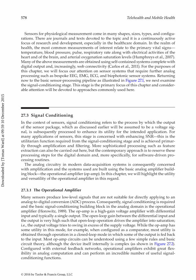
Many sensors produce low-level signals that are not suitable for directly applying to an analog-to-digital conversion (ADC) process. Consequently, signal conditioning is required and the basic signal-conditioning building block in the analog domain is the operational amplifier (Horowitz, 1989). The op-amp is a high-gain voltage amplifier with differential input and typically a single output. The open-loop gain between the differential input and the output is very high such that open-loop operation drives the amplifier into saturation; i.e., the output voltage tries to swing in excess of the supply voltage. While the op-amp has some utility in this mode, for example, when configured as a comparator, most utility is obtained through operation in a closed-loop mode in which some of the output is fed back to the input. Most op-amp circuits can be understood using a few simple rules and basic circuit theory, although the device itself internally is complex (as shown in Figure 27.2). Configured with external feedback networks, operational amplifiers exhibit great flex-ibility in analog computation and can perform an incredible number of useful signal-conditioning functions.
© 2016 by Taylor & Francis Group, LLC
Dow
nloa
ded
by [
Tom
as W
ard]
at 0
9:59
10
Dec
embe
r 20
15
579Sensor Signal Conditioning for Biomedical Instrumentation
The rules for understanding basic op-amp behavior are as follows:
• Rule 1: When the op-amp output is in linear range (for example, when there is negative feedback between output and negative input terminal), the two input terminals are at the same voltage.
• Rule 2: There is no current flow into either input terminal.
Rule 1 applies once there is negative feedback—i.e., connection from v1 to v2.Rule 2 follows from the observation that as the input impedance is infinite (or even if not,
v1 − v2 = 0), there is no input current by Ohm’s law.Application of these relationships can be used to understand the function of important
operational amplifier-based signal-conditioning building blocks.
27.3.2 Signal Amplification with Operational Amplifiers
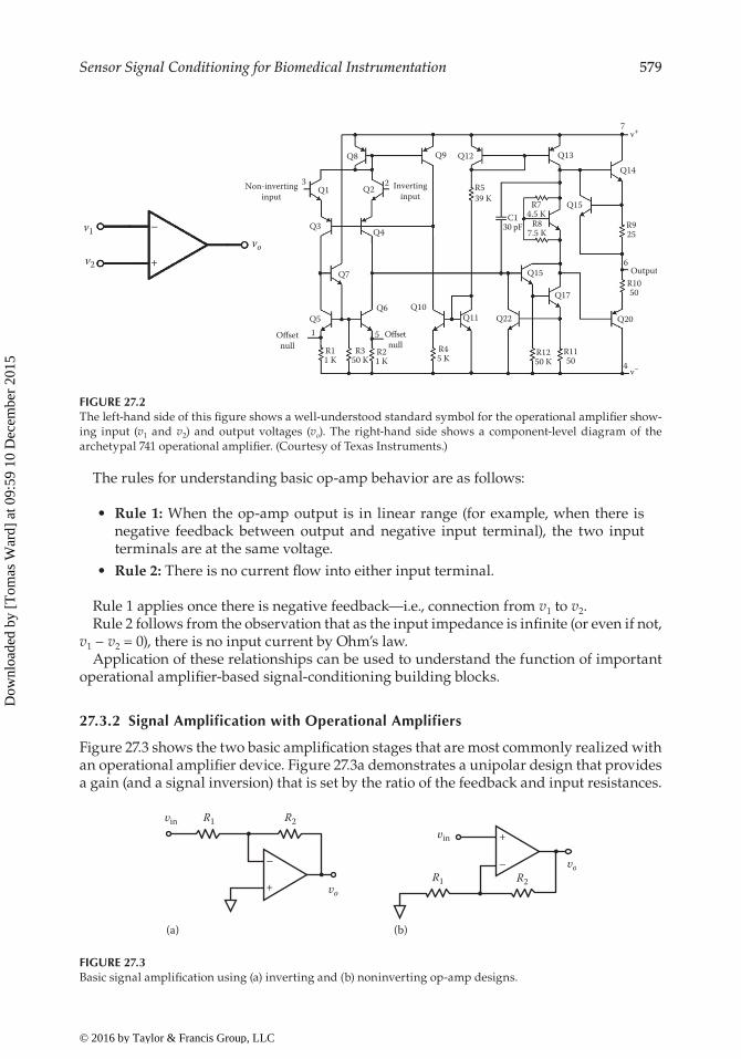
Figure 27.3 shows the two basic amplification stages that are most commonly realized with an operational amplifier device. Figure 27.3a demonstrates a unipolar design that provides a gain (and a signal inversion) that is set by the ratio of the feedback and input resistances.
Q8
Q2
Q10
Q7
Q1
Q3Q4–
+
Invertinginput
Non-invertinginput
Offsetnull
vo
v1
v2
Offsetnull
Q5Q6
Q9 Q12
Q11
Q15
Q22
Q17
Q15
Q13
Q20
Output
2
7
4
6
3
5
R539 K
C130 pF
Q14
R74.5 K
R87.5 K
R925
R1050
R1150
R1250 K
R45 K
R21 K
R350 K
R11 K
1
v+
v−
FIGURE 27.2The left-hand side of this figure shows a well-understood standard symbol for the operational amplifier show-ing input (v1 and v2) and output voltages (vo). The right-hand side shows a component-level diagram of the archetypal 741 operational amplifier. (Courtesy of Texas Instruments.)
υin
υo
υo
R1 R2υin
R1 R2
+
–
+
–
(a) (b)
FIGURE 27.3Basic signal amplification using (a) inverting and (b) noninverting op-amp designs.
© 2016 by Taylor & Francis Group, LLC
Dow
nloa
ded
by [
Tom
as W
ard]
at 0
9:59
10
Dec
embe
r 20
15
580 Telehealth and Mobile Health
Figure 27.3b demonstrates a noninverting configuration—note how the gain is related to the externally connected components.
Application of the basic rules of op-amp analysis in the context of these circuits facilitates an understanding of function. For example, the noninverting amplifier in Figure 27.3b can be understood in the following way: As the difference between the input terminals of the amplifier can be considered zero in this situation, the voltage at the junction of R1 and R2 must be vin. Then, through application of the potential divider relationship, we can say that
vR
R Rvo
1
1 2+= in, (27.1)
vv
RR
o
i
= +1 2
1
. (27.2)
Thus, it is clear that the gain of this amplifier is parameterized by the resistor values R1 and R2. This amplifier has the virtues of positive gain and very high input impedance (essentially that of the op-amp), especially op-amps whose inputs are built with field-effect transistor (FET) technology. Such an amplifier is ideal for situations which require con-ditioning of output from sensors with high output impedance. The same process can be applied to the inverting amplifier:
ivR
i=1
, (27.3)
v iR vRRo i= − = −2
2
1
, (27.4)
vv
RR
o
i
= − 2
1
. (27.5)
Such an amplifier is simple to realize; however, it should be noted that the input resistance is effectively R1, and consequently, there is loading of the signal source that is problematic for sensors characterized by high output impedance. It is worth noting that Equations 27.3 and 27.4 demonstrate that this amplifier can also be considered as a voltage-controlled current source. Such a device is useful for some sensor solutions as part of an excitation circuit (as sug-gested in Figure 27.1). For example, this circuit can form the basis for a LED driver, which is useful when making optical physiological measurements such as in photoplethysmography, pulse oximetry, galvanic skin response, and even brain–computer interfacing (Soraghan et al., 2009). We will also see such a device utilized as part of an optical isolation amplifier later.
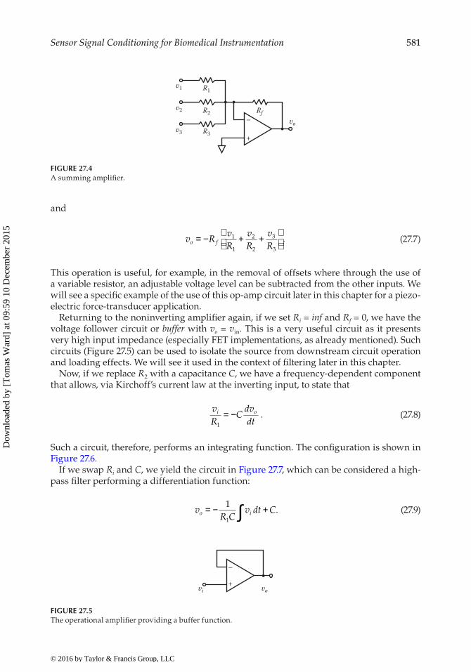
The same basic circuit can be extended further. Through use of Kirchoff’s current law at the negative input, a number of voltage signals can undergo a weighted summation pro-cess as shown in Figure 27.4.
As v− is the same as v+ which is at ground, then we can describe the current at the node represented by the negative terminal of the op-amp as
vR
vR
vR
vR
o
f
1
1
2
2
3
3
+ + = − , (27.6)
© 2016 by Taylor & Francis Group, LLC
Dow
nloa
ded
by [
Tom
as W
ard]
at 0
9:59
10
Dec
embe
r 20
15
581Sensor Signal Conditioning for Biomedical Instrumentation
and
v RvR
vR
vRo f= − + +
1
1
2
2
3
3
. (27.7)
This operation is useful, for example, in the removal of offsets where through the use of a variable resistor, an adjustable voltage level can be subtracted from the other inputs. We will see a specific example of the use of this op-amp circuit later in this chapter for a piezo-electric force-transducer application.
Returning to the noninverting amplifier again, if we set Ri = inf and Rf = 0, we have the voltage follower circuit or buffer with vo = vin. This is a very useful circuit as it presents very high input impedance (especially FET implementations, as already mentioned). Such circuits (Figure 27.5) can be used to isolate the source from downstream circuit operation and loading effects. We will see it used in the context of filtering later in this chapter.
Now, if we replace R2 with a capacitance C, we have a frequency-dependent component that allows, via Kirchoff’s current law at the inverting input, to state that
vR
Cdvdt
i o
1
= − . (27.8)
Such a circuit, therefore, performs an integrating function. The configuration is shown in Figure 27.6.
If we swap Ri and C, we yield the circuit in Figure 27.7, which can be considered a high-pass filter performing a differentiation function:
v
R Cv dt Co i= − +∫1
1
. (27.9)
υ1
υ2
υ3
R1
R2
R3
Rfυo
+
–
FIGURE 27.4A summing amplifier.
υoυi+
–
FIGURE 27.5The operational amplifier providing a buffer function.
© 2016 by Taylor & Francis Group, LLC
Dow
nloa
ded
by [
Tom
as W
ard]
at 0
9:59
10
Dec
embe
r 20
15
582 Telehealth and Mobile Health
Cdvdt
vR
i o
f
= − ; (27.10)
hence,
v R Cdvdto f
i= − . (27.11)
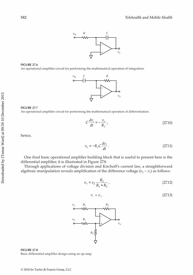
One final basic operational amplifier building block that is useful to present here is the differential amplifier; it is illustrated in Figure 27.8.
Through applications of voltage division and Kirchoff’s current law, a straightforward algebraic manipulation reveals amplification of the difference voltage (v2 − v1) as follows:
v vR
R R+ =+2
2
1 2
, (27.12)
v− = v+. (27.13)
R C
υo
υin
+
–
FIGURE 27.6An operational amplifier circuit for performing the mathematical operation of integration.
υo+
–
RCυin
FIGURE 27.7An operational amplifier circuit for performing the mathematical operation of differentiation.
υ1
υ2
R1
R1
R2
R2
υo+
–
FIGURE 27.8Basic differential amplifier design using an op-amp.
© 2016 by Taylor & Francis Group, LLC
Dow
nloa
ded
by [
Tom
as W
ard]
at 0
9:59
10
Dec
embe
r 20
15
583Sensor Signal Conditioning for Biomedical Instrumentation
The current at the upper node in the figure can be described as follows:
iv v
Rv v
Ro= − = −− +1
1 2
. (27.14)
Substituting for v+ and rearranging yields
v
v vRR
o
2 1
2
1−= . (27.15)
For difference signals, i.e., where v1 ≠ v2, we denote the gain above as differential gain Gd. Notice that for common-mode signals, i.e., v1 − v2 = 0, the gain is zero. This figure is called the common-mode gain, which we denote Gc. Real difference amplifiers do not exhibit Gc = 0 as in practice this is just not possible. Consequently, a figure of merit that can be used to quantify the performance of such amplifiers is the common-mode rejection ratio (CMRR), which is defined as follows:
CMRR = GG
d
c
. (27.16)
The ability to measure the difference between two voltages is particularly useful in the context of measuring electrical potentials in the body. The electrical potential measured at a single location on the human body with respect to a distant reference is termed unipo-lar measurement and can be achieved through the use of amplifiers such as those already described. Commonly, there are significant common-mode signals that can be regarded as noise (particularly mains interference). These can saturate a high-gain amplifier. Consequently in situations where this occurs, differential measurements are made (also referred to as bipolar measurements) instead using the differential amplifier concept.
With the basic building blocks described above, it is possible to perform analog process-ing that may in some cases substitute successfully for digital computation further along the signal chain. The following example illustrates the potential utility in a force-measurement application.
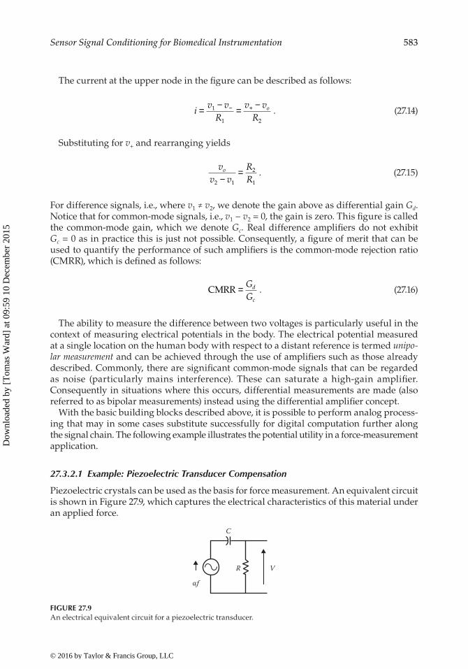
27.3.2.1 Example: Piezoelectric Transducer Compensation
Piezoelectric crystals can be used as the basis for force measurement. An equivalent circuit is shown in Figure 27.9, which captures the electrical characteristics of this material under an applied force.
R V
C
αf
FIGURE 27.9An electrical equivalent circuit for a piezoelectric transducer.
© 2016 by Taylor & Francis Group, LLC
Dow
nloa
ded
by [
Tom
as W
ard]
at 0
9:59
10
Dec
embe
r 20
15
584 Telehealth and Mobile Health
In an approach suggested by Ward and de Paor (1996), an application of Kirchoff’s cur-rent law in this circuit yields
Cddt
f vvR
( )α − = , (27.17)
assuming no current into the amplifier to which the output is connected.Then
RCdvdt
v RCdfdt
+ = α . (27.18)
We can use the Laplace transform to yield an algebraic expression as follows:
v( ) ( )sRC s
RCsF s=
+α
1. (27.19)
This equation is the transfer function that relates the input, in this case an applied force f(t), to the voltage across the input of the amplifier. The effect of this is a filtering process that distorts the original signal. To appreciate this, let us consider a step input to such a transducer and calculate the expected output signal:
f t F t
f t t
m( ) ,
( ) .
= ≥
= <
for
for
0
0 0 (27.20)
Therefore, our force-controlled voltage source is described by
v F t
v t
t
t
i m
i
( )
( )
,
,
= ≥
= <
α for
for
0
0 0 (27.21)
the Laplace transform of which is
v Fs
si m( ) = α 1. (27.22)
Substituting this into the relationship above yields the following output for the voltage across the input of the amplifier in the s domain:
v sF
RCs
m( ) =+
α1
. (27.23)
Using the well-known Laplace transform pair,
1
s ae at
+⇔ − , (27.24)
© 2016 by Taylor & Francis Group, LLC
Dow
nloa
ded
by [
Tom
as W
ard]
at 0
9:59
10
Dec
embe
r 20
15
585Sensor Signal Conditioning for Biomedical Instrumentation
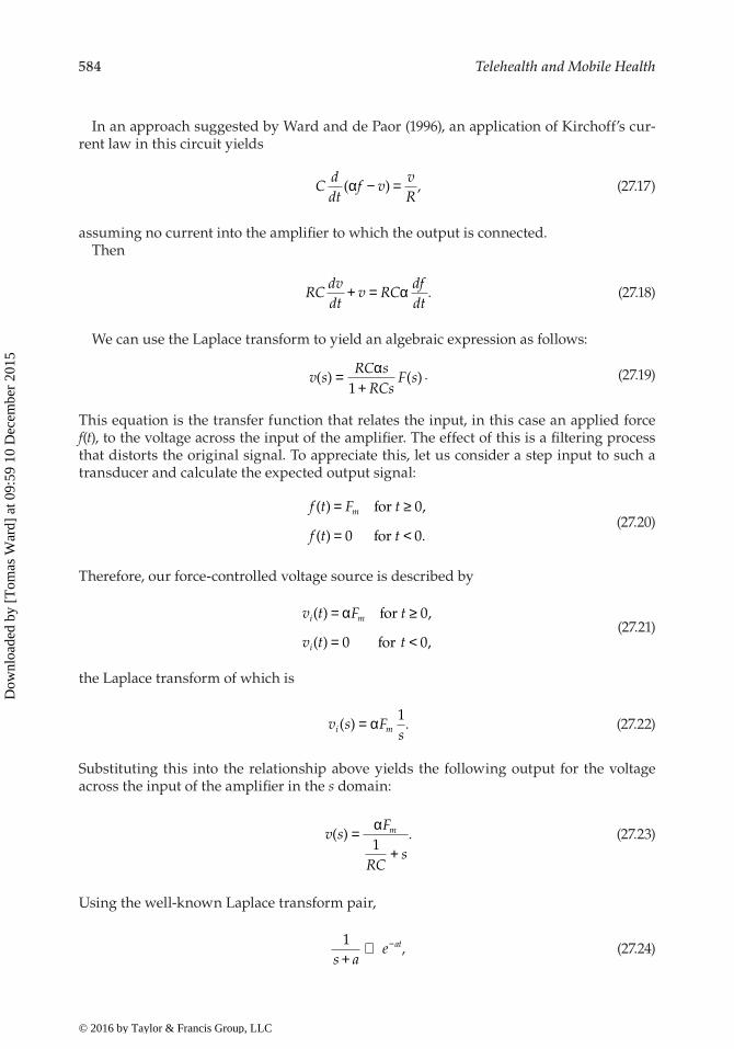
We can recover a time-domain representation of the response to a step (Figure 27.10) as input then as
v(t) = αFme−t/RC (27.25)
Clearly, static loads are not faithfully represented in this particular piezoelectric trans-ducer. It is possible to compensate for such dynamics by using an appropriate condition-ing circuit. If we rearrange Equation 27.19, we can relate the desired force measurement in terms of the voltage produced at the amplifier input as follows:
⇒ = +
αF sRCs
v s( ) ( )11
, (27.26)
Taking the inverse Laplace transform gives us the following relationship, which describes the analog computational operations required to recover f(t):
f t vRC
v t dtt
( ) ( )∝ + ∫1
0
. (27.27)
From an examination of the structure, an appropriate circuit could be designed with the op-amp building blocks already described; for example, a buffer, an integrator, and a sum-ming amplifier can together perform the necessary analog computation.
It should be clear from the discussion so far that op-amps are versatile electronic devices that can be deployed in many ways to implement a wide range of functions in the analog domain. For a deeper exposition of the function of op-amps circuits for measurement and sensor conditioning including a large array of ingenious designs, the reader is referred to textbooks on the topic (Northrop, 2014; Webster, 1998) and application notes from manu-facturers available online. In the next subsection, we will proceed to examine more sophis-ticated electronic conditioning circuits that are ubiquitous in most sensor-processing pipelines. In so doing, we can utilize our appreciation of op-amp circuits to understand how these systems are implemented and indeed how they work.
27.3.3 The Instrumentation Amplifier
The difference amplifier shown in Figure 27.8 is a basic amplifier block that can be extended to measure very small signals differentially in the body. Such measure-ments are the basis behind common connected health signal–acquisition targets such as the electrical activity of the heart (EKG/ECG), those of the muscles (EMG), and that
αfm
t
v
FIGURE 27.10Step response of the piezoelectric crystal model.
© 2016 by Taylor & Francis Group, LLC
Dow
nloa
ded
by [
Tom
as W
ard]
at 0
9:59
10
Dec
embe
r 20
15
586 Telehealth and Mobile Health
of the brain (EEG). All of these signals are characterized by very low signal levels, high common-mode noise levels, and relatively high output impedances. An instrumenta-tion amplifier is a high-performance version of the differential amplifier we have already examined. It is characterized by high common-mode rejection ratio, high input imped-ance, low drift, low noise, and high open-loop gain. It is ideally suited to measurement of the aforementioned signals.
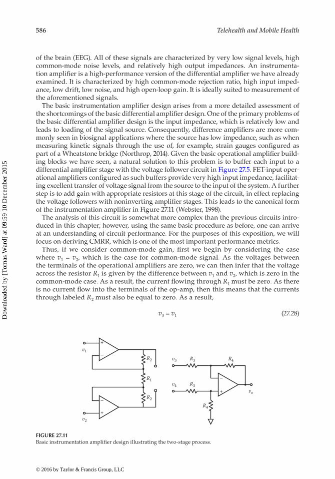
The basic instrumentation amplifier design arises from a more detailed assessment of the shortcomings of the basic differential amplifier design. One of the primary problems of the basic differential amplifier design is the input impedance, which is relatively low and leads to loading of the signal source. Consequently, difference amplifiers are more com-monly seen in biosignal applications where the source has low impedance, such as when measuring kinetic signals through the use of, for example, strain gauges configured as part of a Wheatstone bridge (Northrop, 2014). Given the basic operational amplifier build-ing blocks we have seen, a natural solution to this problem is to buffer each input to a differential amplifier stage with the voltage follower circuit in Figure 27.5. FET-input oper-ational amplifiers configured as such buffers provide very high input impedance, facilitat-ing excellent transfer of voltage signal from the source to the input of the system. A further step is to add gain with appropriate resistors at this stage of the circuit, in effect replacing the voltage followers with noninverting amplifier stages. This leads to the canonical form of the instrumentation amplifier in Figure 27.11 (Webster, 1998).
The analysis of this circuit is somewhat more complex than the previous circuits intro-duced in this chapter; however, using the same basic procedure as before, one can arrive at an understanding of circuit performance. For the purposes of this exposition, we will focus on deriving CMRR, which is one of the most important performance metrics.
Thus, if we consider common-mode gain, first we begin by considering the case where v1 = v2, which is the case for common-mode signal. As the voltages between the terminals of the operational amplifiers are zero, we can then infer that the voltage across the resistor R1 is given by the difference between v1 and v2, which is zero in the common-mode case. As a result, the current flowing through R1 must be zero. As there is no current flow into the terminals of the op-amp, then this means that the currents through labeled R2 must also be equal to zero. As a result,
v3 = v1 (27.28)
υ3
υ4
R4R3
R3
R4
υo+
–
R2
R2
R1
υ1
υ2
–
+
–
+
FIGURE 27.11Basic instrumentation amplifier design illustrating the two-stage process.
© 2016 by Taylor & Francis Group, LLC
Dow
nloa
ded
by [
Tom
as W
ard]
at 0
9:59
10
Dec
embe
r 20
15
587Sensor Signal Conditioning for Biomedical Instrumentation
and
v4 = v2. (27.29)
So we can say that for the front end of the operational amplifier, the common-mode gain Gc = 1.
If we consider differential signals, i.e., v1 ≠ v2, then the analysis becomes a little more involved. As before, the current flow through R1 is determined by the difference between v1 and v2. This same current now flows through the resistors denoted R2. From Ohm’s law we can then see that
v3 − v4 = i(R1 + R2 + R2) (27.30)
and that
v1 − v2 = iR1. (27.31)
This means that the differential gain is as follows:
Gv vv v
R RRd = −
−= +3 4
1 2
1 2
1
2( ) (27.32)
and that the common-mode rejection ratio is
CMRR = = +GG
R RR
d
c
( )1 2
1
2. (27.33)
Finally, the second stage, which is the differential amplifier design considered earlier, provides additional gain determined by the ratio of the resistors R4 and R3, so we can describe the overall gain as
GRR
RR
= +
12 2
1
4
3
. (27.34)
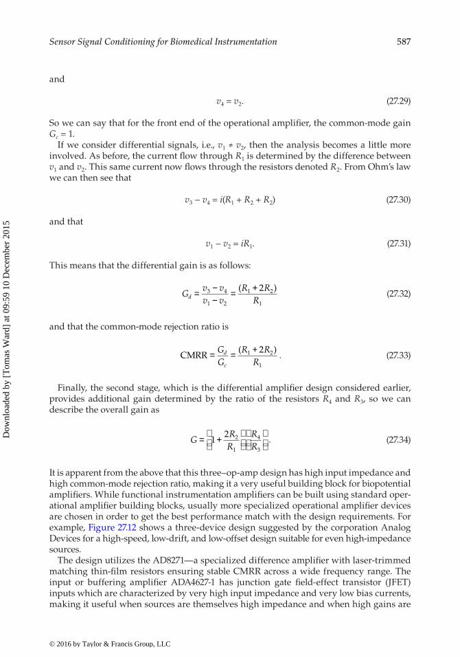
It is apparent from the above that this three–op-amp design has high input impedance and high common-mode rejection ratio, making it a very useful building block for biopotential amplifiers. While functional instrumentation amplifiers can be built using standard oper-ational amplifier building blocks, usually more specialized operational amplifier devices are chosen in order to get the best performance match with the design requirements. For example, Figure 27.12 shows a three-device design suggested by the corporation Analog Devices for a high-speed, low-drift, and low-offset design suitable for even high-impedance sources.
The design utilizes the AD8271—a specialized difference amplifier with laser-trimmed matching thin-film resistors ensuring stable CMRR across a wide frequency range. The input or buffering amplifier ADA4627-1 has junction gate field-effect transistor (JFET) inputs which are characterized by very high input impedance and very low bias currents, making it useful when sources are themselves high impedance and when high gains are
© 2016 by Taylor & Francis Group, LLC
Dow
nloa
ded
by [
Tom
as W
ard]
at 0
9:59
10
Dec
embe
r 20
15
588 Telehealth and Mobile Health
required. It should be noted that a complete (and practical) design would include a decou-pling capacitor network.
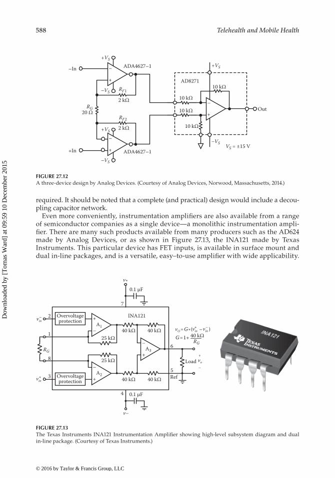
Even more conveniently, instrumentation amplifiers are also available from a range of semiconductor companies as a single device—a monolithic instrumentation ampli-fier. There are many such products available from many producers such as the AD624 made by Analog Devices, or as shown in Figure 27.13, the INA121 made by Texas Instruments. This particular device has FET inputs, is available in surface mount and dual in-line packages, and is a versatile, easy–to-use amplifier with wide applicability.
–VS
–In
+In ADA4627–1
ADA4627–1
AD8271
–VS
–VS
RF 1
RG
2 kΩ
Out
10 kΩ
10 kΩ
10 kΩ
10 kΩ
2 kΩ
20 Ω
+VS
+VS+VS
+
–
+
–
+
–
RF 2
VS = ±15 V
FIGURE 27.12A three-device design by Analog Devices. (Courtesy of Analog Devices, Norwood, Massachusetts, 2014.)
A1
RG
+
–
A2+
–
A3+
–
2 Overvoltageprotection
3
8
Overvoltageprotection
1
vin+
25 kΩ
25 kΩ
40 kΩ 40 kΩ
40 kΩ
7
6
5
Load
4
v–
Ref
0.1 µF
INA121
40 kΩ40 kΩ
vin–
v+
0.1 µF
vO = G * ( – )vin+ vin
–
G = 1+
vo
RG
+
_
FIGURE 27.13The Texas Instruments INA121 Instrumentation Amplifier showing high-level subsystem diagram and dual in-line package. (Courtesy of Texas Instruments.)
© 2016 by Taylor & Francis Group, LLC
Dow
nloa
ded
by [
Tom
as W
ard]
at 0
9:59
10
Dec
embe
r 20
15
589Sensor Signal Conditioning for Biomedical Instrumentation
Usually data sheets for such devices will express CMRR through the related term common-mode rejection (CMR), which is understood as follows:
CMR = 20 log10 (CMRR). (27.35)
CMR for good-quality monolithic instrumentation amplifiers exceed 100 dB. The devel-opment of the instrumentation amplifier circuit on the same die facilitates the use of laser-trimmed resistors and better matching components throughout, which gives greater resistance to temperature variation. Such developments are leading to very high-accuracy devices that are being increasingly refined to meet modern healthcare tech-nology demands. The presentation here gives only a brief introduction and interested readers should consult application notes from major semiconductor companies for solutions specific to their needs.
27.4 The Analog-to-Digital Conversion Process
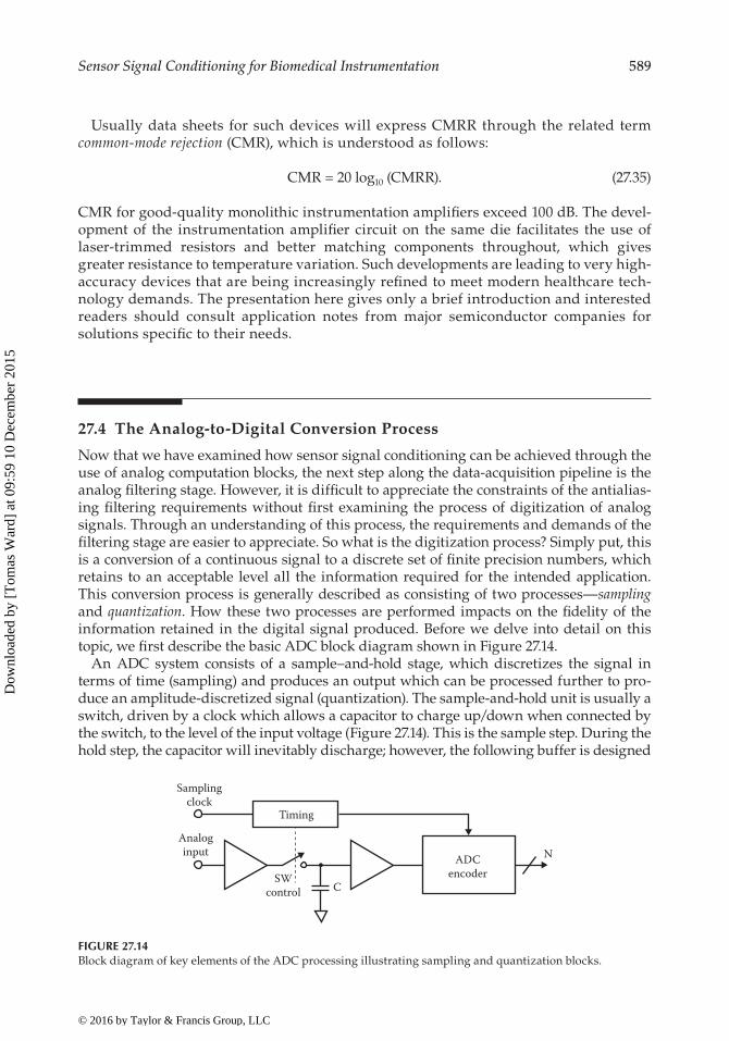
Now that we have examined how sensor signal conditioning can be achieved through the use of analog computation blocks, the next step along the data-acquisition pipeline is the analog filtering stage. However, it is difficult to appreciate the constraints of the antialias-ing filtering requirements without first examining the process of digitization of analog signals. Through an understanding of this process, the requirements and demands of the filtering stage are easier to appreciate. So what is the digitization process? Simply put, this is a conversion of a continuous signal to a discrete set of finite precision numbers, which retains to an acceptable level all the information required for the intended application. This conversion process is generally described as consisting of two processes—sampling and quantization. How these two processes are performed impacts on the fidelity of the information retained in the digital signal produced. Before we delve into detail on this topic, we first describe the basic ADC block diagram shown in Figure 27.14.
An ADC system consists of a sample–and-hold stage, which discretizes the signal in terms of time (sampling) and produces an output which can be processed further to pro-duce an amplitude-discretized signal (quantization). The sample-and-hold unit is usually a switch, driven by a clock which allows a capacitor to charge up/down when connected by the switch, to the level of the input voltage (Figure 27.14). This is the sample step. During the hold step, the capacitor will inevitably discharge; however, the following buffer is designed
N
C
ADCencoder
Timing
SWcontrol
Samplingclock
Analoginput
FIGURE 27.14Block diagram of key elements of the ADC processing illustrating sampling and quantization blocks.
© 2016 by Taylor & Francis Group, LLC
Dow
nloa
ded
by [
Tom
as W
ard]
at 0
9:59
10
Dec
embe
r 20
15
590 Telehealth and Mobile Health
to have sufficiently high input impedance such that it discharges by a tolerable amount (< 1 least significant bit [LSB]) during this time. During this hold time, the encoder produces an N-bit representation of the sampled signal resulting in an amplitude discretization.
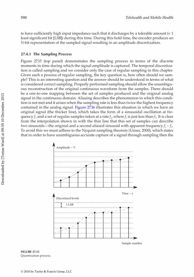
27.4.1 The Sampling Process
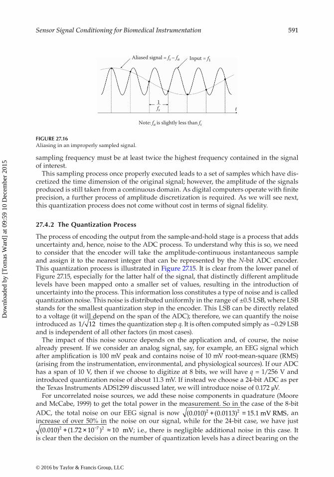
Figure 27.15 (top panel) demonstrates the sampling process in terms of the discrete moments in time during which the signal amplitude is captured. The temporal discretiza-tion is called sampling and we consider only the case of regular sampling in this chapter. Given such a process of regular sampling, the key question is, how often should we sam-ple? This is an interesting question and the answer should be understood in terms of what is considered correct sampling. Properly performed sampling should allow the unambigu-ous reconstruction of the original continuous waveform from the samples. There should be a one-to-one mapping between the set of samples produced and the original analog signal in the continuous domain. Aliasing describes the phenomenon in which this condi-tion is not met and it arises when the sampling rate is less than twice the highest frequency contained in the analog signal. Figure 27.16 illustrates this situation in which we have an original signal (the thicker line), which takes the form of a sinusoidal oscillation at fre-quency f1 and a set of regular samples taken at a rate fs, where fs is just less than f1. It is clear from the interpolation shown in with the thin line that this set of samples can describe two sinusoids—the original and a second aliased sinusoid with apparent frequency fs − f1. To avoid this we must adhere to the Nyquist sampling theorem (Unser, 2000), which states that in order to have unambiguous accurate capture of a signal through sampling then the
Sample number
Time – s
Amplitude – V
Discretized levels
1 LSB
FIGURE 27.15Quantization process.
© 2016 by Taylor & Francis Group, LLC
Dow
nloa
ded
by [
Tom
as W
ard]
at 0
9:59
10
Dec
embe
r 20
15
591Sensor Signal Conditioning for Biomedical Instrumentation
sampling frequency must be at least twice the highest frequency contained in the signal of interest.
This sampling process once properly executed leads to a set of samples which have dis-cretized the time dimension of the original signal; however, the amplitude of the signals produced is still taken from a continuous domain. As digital computers operate with finite precision, a further process of amplitude discretization is required. As we will see next, this quantization process does not come without cost in terms of signal fidelity.
27.4.2 The Quantization Process
The process of encoding the output from the sample-and-hold stage is a process that adds uncertainty and, hence, noise to the ADC process. To understand why this is so, we need to consider that the encoder will take the amplitude-continuous instantaneous sample and assign it to the nearest integer that can be represented by the N-bit ADC encoder. This quantization process is illustrated in Figure 27.15. It is clear from the lower panel of Figure 27.15, especially for the latter half of the signal, that distinctly different amplitude levels have been mapped onto a smaller set of values, resulting in the introduction of uncertainty into the process. This information loss constitutes a type of noise and is called quantization noise. This noise is distributed uniformly in the range of ±0.5 LSB, where LSB stands for the smallest quantization step in the encoder. This LSB can be directly related to a voltage (it will depend on the span of the ADC); therefore, we can quantify the noise introduced as 1 12/ times the quantization step q. It is often computed simply as ~0.29 LSB and is independent of all other factors (in most cases).
The impact of this noise source depends on the application and, of course, the noise already present. If we consider an analog signal, say, for example, an EEG signal which after amplification is 100 mV peak and contains noise of 10 mV root-mean-square (RMS) (arising from the instrumentation, environmental, and physiological sources). If our ADC has a span of 10 V, then if we choose to digitize at 8 bits, we will have q = 1/256 V and introduced quantization noise of about 11.3 mV. If instead we choose a 24-bit ADC as per the Texas Instruments ADS1299 discussed later, we will introduce noise of 0.172 μV.
For uncorrelated noise sources, we add these noise components in quadrature (Moore and McCabe, 1999) to get the total power in the measurement. So in the case of the 8-bit ADC, the total noise on our EEG signal is now ( . ) ( . ) .0 010 0 0113 15 12 2+ = mV RMS, an increase of over 50% in the noise on our signal, while for the 24-bit case, we have just
( . ) ( . ) 0 010 1 72 10 102 7 2+ × ≈− mV; i.e., there is negligible additional noise in this case. It is clear then the decision on the number of quantization levels has a direct bearing on the
t
Aliased signal = fs – fa Input = f1
Note: fa is slightly less than fs
fs1
FIGURE 27.16Aliasing in an improperly sampled signal.
© 2016 by Taylor & Francis Group, LLC
Dow
nloa
ded
by [
Tom
as W
ard]
at 0
9:59
10
Dec
embe
r 20
15
592 Telehealth and Mobile Health
amount of noise introduced; however, the impact of this noise must be judged with respect to the noise already on the signal and the amount of noise which can be tolerated in the application.
After these digitization issues have been thought through for a specific application, an important and sometimes neglected aspect of the ADC process is the prefiltering of the signals with an appropriate antialiasing filter. This topic is considered next and should be considered in tandem with the sampling requirements.
27.4.3 Antialiasing Filters
A filter is, in the context of this discussion, an electrical circuit which alters the spectral composition of the signal upon which it operates. Filters are usually used to attenuate unwanted spectral ranges, although they can also be used to increase signal power in specific bands. Sometimes both are required. Filters can take the form of single passive circuits containing few elements to complex systems requiring sophisticated analysis to model fully.
Analog filters are a critical component of the data-acquisition pipeline. While they can be used at any point in the pipeline to enhance the signals of interest and suppress artifact— for example, a common use is a notch filter for removing the effects of 50 Hz (or 60 Hz) mains interference (Sweeney et al., 2012b)—in this chapter we focus primarily on their utility in ensuring that we achieve proper sampling as defined in Subsection 27.4.1. The reader will recall that in order to prevent aliasing, we must ensure that the signal to be sampled contains no components higher than half the sampling rate. To ensure that this is indeed the case, we use a filter with a low-pass cutoff suitably chosen such that the signal has no significant components above this special frequency. Such a filter is called an anti-aliasing filter and it is placed right before the ADC unit as shown in Figure 27.1.
Given that the requirement of an antialiasing filter is to meet stop-band attenuation lev-els at a frequency corresponding to half the sample rate, then there are many filter designs which can meet such a criterion. In this subsection, we give a brief introduction to some practical ideas here, beginning with the simplest filter possible—the passive RC first-order filter shown in Figure 27.17.
The filtering behavior of the passive RC low-pass filter can be understood easily by using the potential divider approach and Laplace equivalents in the s domain for the circuit com-ponents. Thus, using the potential divider approach and rearranging, we have
vv
sC
sCR sRC
o
i
=+
=+
1
11
1. (27.36)
υoυi
R
C
FIGURE 27.17A first-order passive RC low-pass filter.
© 2016 by Taylor & Francis Group, LLC
Dow
nloa
ded
by [
Tom
as W
ard]
at 0
9:59
10
Dec
embe
r 20
15
593Sensor Signal Conditioning for Biomedical Instrumentation
If we next consider the magnitude of the response, as a function of frequency, we calculate
vv sRC j RC RC
o
i
=+
=+
=+
11
11
1
1 2ω ω( ). (27.37)
From this we can see that at DC when ω = 0 that the gain is 1 and that as ω tends larger, the gain increasingly diminishes, demonstrating that this is indeed a low-pass filter. The cutoff frequency, which is defined as the half-power frequency, can then be derived as
vv RC
o
i
2
2
12
11
= =+ ( )ω
, (27.38)
which is equivalent for ω = 1/RC rad/s or f = 1/2πRC in hertz.This is a first-order passive low-pass filter with a roll-off of 20 dB/decade. This basic fil-
tering unit can be cascaded to create higher-order and, hence, steeper roll-off designs, although to prevent loading effects, the buffer amplifier, as shown in Figure 27.5, should be used to isolate the stages. A second-order implementation of this is shown in Figure 27.18.
The preceding filters are pretty good for many antialiasing filtering needs; however, it is common to utilize filter designs that allow good trade-offs between filter characteristics that are specific to various application requirements. To better capture these ideas, we next examine a number of key analog filter design parameters (as in Figure 27.19) that we will refer to when considering these standard designs.
υo
+
–C
R+
–C
Rυi
FIGURE 27.18A second-order passive RC low-pass filter.
εfCUTOFF
fSTOP
Stop bandTransitionband
Passband
P = filter order
Frequency (Hz)
Amax
ASTOP
APASS
Gai
n (d
B)
FIGURE 27.19Analog filter design parameters.
© 2016 by Taylor & Francis Group, LLC
Dow
nloa
ded
by [
Tom
as W
ard]
at 0
9:59
10
Dec
embe
r 20
15
594 Telehealth and Mobile Health
Figure 27.19 shows the key parameters of a low-pass filter that are relevant to the design of antialiasing solutions. The cutoff frequency fc referred to earlier is indicated as a corner frequency in the top right of the plot. The passband refers to the frequency range from DC to fc. The stop-band frequency fs is the point at which the minimum attenuation is first reached for the filter. The magnitude of the gain in the passband is referred to here as Ap, while the gain in the stop band is referred to as As. Both are usually expressed in decibels. Some filter designs have a ripple in either or both of the passband and the stop band. The magnitude of this ripple is represented here as ε. In filters with ripple, Ap and As refer to the minimum and maximum gains in their respective bands. An important design parameter is Amax, which represents the dynamic range or difference between the passband and stop-band gains (i.e., Amax = Ap − As). Finally, as the filter response extends beyond the cutoff frequency, it falls through what is referred to as the transition band to the stop-band region. The bandwidth of the transition band is determined by the precise filter design and the order (P) of the filter. As a general rough and conservative guide, the final rate of power roll-off is 20 dB/decade per pole. The filter order is determined by the number of poles in the transfer function. For instance, if a filter has two poles in its transfer function, it is described as a second-order filter.
As more poles are added and, hence, higher order is achieved, the transition bandwidth reduces and will approach the ideal “brick-wall” filter characteristic. This would suggest one should use a very high-order filter; however, as Figure 27.18 illustrates, every pole involves additional circuitry with a concomitant impact on noise, offsets, power. and bulk. Usually appropriate minimal designs are chosen based on the application needs and can proceed as follows.
As a general rule of thumb, we can estimate the order of the filter required for a particu-lar application as
PA
ffs
c
=
max
20210log
, (27.39)
where the brackets used indicate rounding up. This is a conservative (as it assumes that there is full signal power at and above half the sampling rate) but useful starting point in filter design. The calculation is based on the observation that the roll-off can be estimated as 20 dB/decade per pole and we can conservatively set fstop as equal to fs/2 so that we have maximum attenuation at the desired frequency (half the sampling rate). Figure 27.20 helps illustrate this idea.
For example, let us consider that we have an EEG signal requiring sampling at 500 Hz, which means that we need to ensure that there is negligible signal above half the sampling rate. If we consider that there are no EEG components above 100 Hz of interest and that we need Amax of at least 60 dB, then
P =
=60
20500
2 100
8
10log( )
. (27.40)
Thus, we should use an eighth-order filter. Of course, when one considers the use of a fil-ter, it is appropriate to think of what filter precisely one should use. As mentioned earlier,
© 2016 by Taylor & Francis Group, LLC
Dow
nloa
ded
by [
Tom
as W
ard]
at 0
9:59
10
Dec
embe
r 20
15
595Sensor Signal Conditioning for Biomedical Instrumentation
there are a number of standard designs that offer compromise in terms of the filter param-eters described earlier. The most common filter designs are the following:
• Butterworth• Chebyshev• Bessel
Each of these filter designs represents a trade-off between roll-off, passband ripple, and step response. To understand why this is so, it requires an in-depth examination of the underlying mathematical models underpinning the design. This is a topic which cannot be covered here due to space constraints but interested readers can consult any standard text on analog circuits for an exposition of the principals involved (Smith, 1997). The basic trade-offs are described very succinctly below:
• Roll-off: Roll-off describes the width of the transition band in a filter design. The ideal filter has a transition band of zero and is thought of as a brick-wall filter. Such ideal filters are not realizable in practice, but as we have seen, real filters have a roll-off that can be improved through increasing the filter order.
A simple rule of thumb which allows one estimation of the required order for a given filtering need has already been presented. However, it should be stressed that this is only approximate and that the precise roll-off behavior of a filter can be improved through various methods, such as, for example, introducing ripple into the filter band. The Chebyshev filter is an example of this, and of the three designs, it presents the best roll-off; i.e., for a given filter order the transition band is short-est in this design.
• Passband ripple: The passband of a filter should ideally be flat. As we have seen, the Chebyshev filter sacrifices a flat passband for faster roll-off. The Butterworth filter, on the other hand, has been designed to have the shortest possible transition band while still maintaining a flat passband; i.e., there is no ripple. The Bessel filter also has a flat passband; however, it has the worst roll-off of the three designs.
• Step response: Many filters designs exhibit ringing when subjected to an abruptly changing input such as in a step response test. The Bessel filter has been designed to minimize overshoot and ringing compared to the Butterworth and Chebyshev (worst performing in this regard) and this has come at the cost of the roll-off performance.
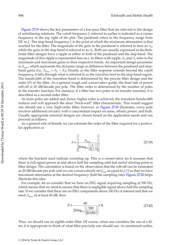
fa
DR
DRP =
fs
fs2fa
6log2
fs2
Slope = 6M dB/octaveP = filter orderDR = dynamic range (dB)fa = fpass , fs/2 = fstop
FIGURE 27.20Filter order determination using Equation 27.39.
© 2016 by Taylor & Francis Group, LLC
Dow
nloa
ded
by [
Tom
as W
ard]
at 0
9:59
10
Dec
embe
r 20
15
596 Telehealth and Mobile Health
Now, given that these designs represent trade-offs between these filter characteristics, how should the filter choice be decided? This depends, understandably, on how these fil-ter characteristics impact on the information bearing aspect of the signals in question. If the relevant information in a signal is embedded in terms of its spectral content, then it is important to reduce the possibilities of frequency-dependent distortion in the passband as it will lead to uncertainty in the interpretation of the information. Many EEG studies, for example, make use of the relative powers in a finite set of relatively narrow bands. For such applications, aliasing has significant impact and so aggressive roll-off filters such as Chebyshev or Butterworth (which, in addition, has flat passband) are preferred in these applications. Other signals such as the ECG, for example, are best characterized in terms of their time-domain features, such as the QRS complex. For such applications, the Bessel fil-ter is usually the best choice as it can best retain information about such temporal features without undue distortion dues to its superior step response. For applications in which the signals contain time-varying spectral components, a popular compromise is to use a Butterworth filter. The Butterworth design is a good all-around filter.
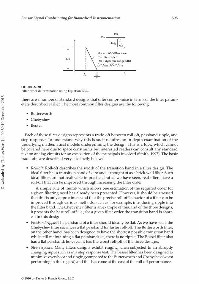
These filter designs can be readily implemented using an op-amp circuit building block called the Sallen–Key filter—the design of which is shown in Figure 27.21 (Sallen and Key, 1955). Using this building block, which is a two-pole unit, all of the above filter designs can be implemented to a high order using suitable values for the resistors and capacitors. Increasing order is achieved simply by cascading stages and order-specific component values.
From a mathematical analysis, one can calculate the appropriate values of resistors and capacitors to achieve Sallen–Key implementations for the filter designs discussed here. However, a much more convenient way to design such a filter is to use the many design tools available online which will, upon specification of the required filter parameters, pro-duce a detailed design including a bill of materials. Further, for many applications, single integrated circuit filter solutions, especially in the form of switched capacitor implementa-tions, are very convenient where a clock signal is available. Their versatility, performance, and compact form factor make them an excellent choice for many. The switched capacitor filter is a mix of analog and digital components and it is from this mix that it derives its flexibility. We continue this theme of distributing function across the analog and digital domains through presenting next a brief discussion of the merits of oversampling and decimation.
υi R2R1
R3
R4
υo
+
–C2
C1
FIGURE 27.21The Sallen–Key two-pole building block for active filter design.
© 2016 by Taylor & Francis Group, LLC
Dow
nloa
ded
by [
Tom
as W
ard]
at 0
9:59
10
Dec
embe
r 20
15
597Sensor Signal Conditioning for Biomedical Instrumentation
27.4.4 Oversampling and Decimation
There is a tendency to reduce the amount of analog circuitry in modern connected health systems. Surfeit bandwidth and computational capacity, both local and remote, means that many operations which hitherto might have been performed using analog circuitry can now take place in the digital domain, reducing sensor node complexity and bulk. The complexity of the device impacts unit cost, failure modes, and device fixes. In terms of the last one, this is an important consideration; for example, a sensor-conditioning opera-tion requiring replacement or update implemented in the digital domain can be upgraded via a firmware upgrade possibly implemented over the air. An analog implementation, in contrast, requires that the sensor is sent back for replacement or upgrading. This is a logistically far more complex and usually expensive task. The reduction in sensor node volume and weight associated with a reduction in circuitry has benefits in producing a smaller, and more wearable, device, which can improve user compliance, depending on the specific application. Finally, it should be noted the net reduction in sensor node bulk through removal of analog components can be even greater than accounted for by the circuitry alone, as often the associated battery requirements can be reduced to enable even greater savings. The precise nature of this particular type of saving is not guaranteed as it depends on the implementation of the processing off-loaded to the digital domain—this processing may incur additional power in terms of the digital implementation and/or transmission. While it is important then to carefully consider all aspects when deciding the analog/digital breakdown, the current trend is to reduce analog requirements through digital means. An interesting example of this is demonstrated in the area of antialiasing we have just looked at.
27.4.4.1 Oversampling
From consideration of our basic antialiasing filter design equation, Equation 27.38, we can see that one way to simplify the filter design required is to push out fs/2 such that the roll-off can be less aggressive and, therefore, fewer poles are required. This necessitates sampling at rates higher than the minimum required—this would normally be twice the highest frequency of interest in the signal to be sampled. The use of a much higher sam-pling rate to accommodate a gentler filter roll-off is called oversampling; and given the power of modern digital signal processing (DSP), which can accommodate very high sam-ple rates and high-throughput ADCs, it is something which can be done relatively easily for most biosignals. However, there is a lot of redundant information in the data stream produced which without compression (which requires computation), will have an impact on bandwidth needs if we are considering a connected health application. An alternative idea which also provides an opportunity to touch upon the versatility and utility of digital filtering is a technique called multisampling, which is a combination of oversampling and decimation.
27.4.4.2 Multisampling
Multirate sampling makes use of both oversampling and decimation to provide a relax-ation on both the analog filtering requirements for antialiasing and the final data rate at the system output. The process works by oversampling first. Usually some multiple of the final desired data rate, which we consider, as before, as fs is used. This relaxes the roll-off requirement by pushing out half the sampling rate used in Equation 27.40. Let us call this
© 2016 by Taylor & Francis Group, LLC
Dow
nloa
ded
by [
Tom
as W
ard]
at 0
9:59
10
Dec
embe
r 20
15
598 Telehealth and Mobile Health
rate k · fs. Now, immediately following the ADC, we can implement a digital filter which will seek to implement the original required antialiasing function for fs/2. Digital filters can accommodate very sharp cutoffs and high order relative to their analog counterparts. In addition, they are easy to implement and flexible. As a result of this operation, the resul-tant digital signal is highly oversampled yet contains insignificant signal above fs/2. There is now considerable redundancy; however, this redundancy can be removed through the simple process of decimation. In this case we can retain every kth sample and lose the rest. Let us consider the EEG example already considered. If we push the sample rate from 500 Hz to 2 kHz, then we now need use only a third-order filter to achieve the necessary antialiasing requirements. We now have an unusable band between 100 Hz and 1 kHz. We can now design and use a digital filter with a cutoff of 100 Hz to remove these components and revert to our original desired data rate by a decimation process that retains only one out of every four samples.
The above approach highlights very well the additional benefits that can be accrued from considering the sensor-processing pipeline from both analog and digital domains simultaneously. The idea of hybrid analog and digital processing done in a tightly coupled integrated fashion is increasingly alluring for both device manufacturers, who can now provide (and sell) complete solutions, and engineers, who can benefit from smaller foot-print designs and simpler design phases. We briefly examine this phenomenon next as it is a logical progression to the material presented so far and is a signpost toward future developments in sensor processing relevant to the field of connected health.
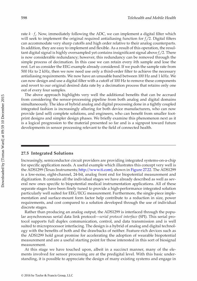
27.5 Integrated Solutions
Increasingly, semiconductor circuit providers are providing integrated systems-on-a-chip for specific application needs. A useful example which illustrates this concept very well is the ADS1299 (Texas Instruments; http://www.ti.com), shown in Figure 27.22. The ADS1299 is a low-noise, eight-channel, 24-bit, analog front end for biopotential measurement and digitization. It contains all the individual stages we have already described as well as sev-eral new ones specific to biopotential medical instrumentation applications. All of these separate stages have been finely tuned to provide a high-performance integrated solution particularly well suited for EEG/ECG measurement. Furthermore, the single-piece imple-mentation and surface-mount form factor help contribute to a reduction in size, power requirements, and cost compared to a solution developed through the use of individual discrete stages.
Rather than producing an analog output, the ADS1299 is interfaced through the popu-lar asynchronous serial data link protocol—serial protocol interface (SPI). This serial pro-tocol supports full duplex communication, control, and data transmission and is well suited to microprocessor interfacing. The design is a hybrid of analog and digital technol-ogy with the benefits of both and the drawbacks of neither. Feature-rich devices such as the ADS1299 hold great promise for accelerating the adoption of wearable biopotential measurement and are a useful starting point for those interested in this sort of biosignal measurement.
At this stage we have touched upon, albeit in a succinct manner, many of the ele-ments involved for sensor processing are at the predigital level. With this basic under-standing, it is possible to appreciate the design of many existing systems and engage in
© 2016 by Taylor & Francis Group, LLC
Dow
nloa
ded
by [
Tom
as W
ard]
at 0
9:59
10
Dec
embe
r 20
15
599Sensor Signal Conditioning for Biomedical Instrumentation
the development of new applications. However, primarily because of its importance at the hardware level, we will briefly visit the user safety and the design of appropriate circuits which can help isolate human subjects from risk of shock and other hazards associated with electrical energy. A motivating factor here is that the availability and reduction in the cost of so many sensors and sensor-processing modules is leading to a huge growth in experimentation and applications of sensor processing for health and wellness applications. The ease with which people can try out these sensors may lead to overenthusiastic adoption and implementation without due care and attention to some of the more mundane yet complex aspects of the design, such as those for subject safety. Section 27.6 provides a short introduction to some of the solutions which are available and which should be integrated, when appropriate to sensor systems, which will be used with human subjects.
+
–
A1 ADC1
A2
MUX
REF
Inpu
ts
ADC2
A3 ADC3
A4 ADC4
A5 ADC5
A6 ADC6
A7 ADC7
Control
Test signals andmonitors
SPI
SPIC
LKQ
PIO and controller
A8 ADC8To channel
Patient bias and reference
Reference
Oscillator
FIGURE 27.22ADS1299 internal architecture. (Courtesy of Texas Instruments.)
© 2016 by Taylor & Francis Group, LLC
Dow
nloa
ded
by [
Tom
as W
ard]
at 0
9:59
10
Dec
embe
r 20
15
600 Telehealth and Mobile Health
27.6 Isolation Circuits
For safety, it is important to protect the user from the hazards of electrical shock. While this seems obvious, it is often an afterthought, especially at the research and prototyping stage. Electrical shock can always present a safety risk with electrical circuits and it is important to consider the problem seriously. It is worth highlighting that it is current, not voltage, which is the real hazard here. Current flow in tissue can cause excessive resistive heating (P = I2R effects), leading to burns, electrochemical heating, and electrical stimula-tion of neuro muscular systems. In the case of electrical stimulation, there are obvious and potentially lethal dangers. For example, even 100 mA of current can lead to disruption to the delicately balanced patterns of neuromuscular interaction which govern the proper functioning of the heart. Even lower levels ~15 mA can lead to respiratory disruption, including paralysis.
Instrument front ends including sensors which may make electrical contact with the patient must be completely isolated from the mains power supply by a nonconducting bar-rier. This barrier must be able to withstand potential differences of several thousand volts. Isolation is accomplished by separating the input stage of the isolation amplifier from the output stage in a galvanic sense. Such a requirement necessitates that the input stage has a separate, floating power supply and a return path that is connected to the output stage of the isolation amplifier by a very high resistance and a parallel capacitance in the picofarad range. Similarly, and appropriately, high impedance isolates the input signal terminals of the front end from the output of the isolation amplifier.
27.6.1 Methods of Isolation
There are three principal means of implementing the required coupling:
• Optical• Capacitive• Magnetic
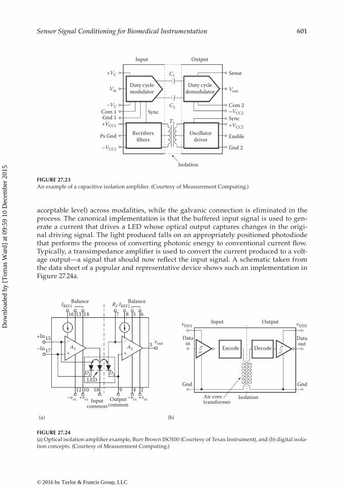
27.6.1.1 Capacitive Isolation Amplifiers
An example of a capacitive isolation amplifier is shown in Figure 27.23. The basic idea here is simply to modulate the input signal up into a band, and via a modulation scheme, which allows high-fidelity signal transmission across isolating capacitors. The output section then must demodulate the transmitted signal in order to recover the original biosignal. The precise implementation detail (for example, how modulation is accomplished) varies but the basic concept remains. In many designs, the power lines are isolated through an isolation transformer.
27.6.1.2 Optical Isolation Amplifiers
While implementation details again here can vary, the basic concept is straightforward and involves the conversion of electrical energy to optical energy and back again. The information in the analog signal is faithfully maintained (or at least maintained to an
© 2016 by Taylor & Francis Group, LLC
Dow
nloa
ded
by [
Tom
as W
ard]
at 0
9:59
10
Dec
embe
r 20
15
601Sensor Signal Conditioning for Biomedical Instrumentation
acceptable level) across modalities, while the galvanic connection is eliminated in the process. The canonical implementation is that the buffered input signal is used to gen-erate a current that drives a LED whose optical output captures changes in the origi-nal driving signal. The light produced falls on an appropriately positioned photodiode that performs the process of converting photonic energy to conventional current flow. Typically, a transimpedance amplifier is used to convert the current produced to a volt-age output—a signal that should now reflect the input signal. A schematic taken from the data sheet of a popular and representative device shows such an implementation in Figure 27.24a.
Sync
Isolation
Output
Duty cycledemodulator
Duty cyclemodulator
Oscillatordriver
Rectifiersfilters
Sense
Com 2
Gnd 2
Enable
Sync
Input
C1
T1
C2
Vout
–VCC2
+VCC2
Gnd 1
Ps Gnd
Com 1
Vin
–VCC1
+VC
–VC
+VCC1
FIGURE 27.23An example of a capacitive isolation amplifier. (Courtesy of Measurement Computing.)
A1
IREF1 RF IREF2Balance Balance
15
16 13 14 7 8 5 6
3
12 10 18 9 4
Inputcommon
Outputcommon
2
17
–
+A2
D2D1LED
–
+
+In
–In
–vcc +vcc –vcc +vcc
Output
Dataout
IsolationAir coretransformer
Input
Encode Decode
GndGnd
vDD2vDD1
Datainvout
(a) (b)
FIGURE 27.24(a) Optical isolation amplifier example, Burr Brown ISO100 (Courtesy of Texas Instrument), and (b) digital isola-tion concepts. (Courtesy of Measurement Computing.)
© 2016 by Taylor & Francis Group, LLC
Dow
nloa
ded
by [
Tom
as W
ard]
at 0
9:59
10
Dec
embe
r 20
15
602 Telehealth and Mobile Health
27.6.1.3 Magnetic Isolation Amplifiers
Magnetic isolation amplifiers incorporate some of the basic ideas from both the capaci-tive and optical isolators. Like their optical counterparts, the basic mechanism by which isolation is achieved is through a transducer process in which energy is converted from one form into another in such a way as to eliminate galvanic connections. In a magnetic isolation amplifier, the specific means involves conversion of the voltage signal at the input to a current that is then used to generate changes in a magnetic field. Similarly as in the capacitive isolation amplifier design, this current signal is used to modulate a carrier such that there is a good coupling between the input and output stages via the bridging mechanism—in this case a coil which will either form one side of a transformer or a giant magnetoresistor bridge. In either case, the output is a voltage signal that reflects the origi-nal input voltage signal.
27.6.1.4 Digital Isolation
The techniques for achieving isolation that are already described have all operated directly with the analog biosignal. The same ideas can be used with digital signals, and in such cases, digital data are transmitted across the isolation barrier. A representative schematic is shown in Figure 27.24b.
It is clear then that there are a range of solutions available to provide subject safety when operating a sensor-processing pipeline at the hardware level. As all these solutions are available inexpensively from companies such as Texas Instruments and Maxim, to name but a few, there is no excuse for not giving this aspect of the sensor-processing system as much care and diligence as the other components we have already seen. Even with battery-operated technology, it is always important to be aware of the risks and potentials for harm with any sensor technology processing circuitry and to design accordingly.
27.7 Conclusions
This chapter has presented a whirlwind tour of the more fundamental stages in the pro-cessing of sensors for medical instrumentation purposes with an emphasis on consid-erations relevant to connected health and wellness applications. Such systems present challenges in terms of instrumentation size, power consumption characteristics, and abil-ity to maximize SNR. The chapter has primarily focused on the analog domain, although discussion of the synergetic impact available through consideration of processing in both the digital and analog domains, where appropriate, has also been presented. In terms of the primary analog focus, the chapter demonstrates the versatility of analog process-ing using the classic building block of the operational amplifier. The basic introduction to the operational amplifier serves both the purpose of demonstrating the preprocessing possibilities in the analog domain and the laying of conceptual foundations which sup-port better understanding of newly available, powerful, and consequently complex single monolithic integrated circuits. These modern devices will increasingly be used as the core processing elements for modern and future sensor applications. The short introduction to the sampling and quantization process is practical and usable for most applications although it does not touch on modern concepts in sampling systems such as irregular
© 2016 by Taylor & Francis Group, LLC
Dow
nloa
ded
by [
Tom
as W
ard]
at 0
9:59
10
Dec
embe
r 20
15
603Sensor Signal Conditioning for Biomedical Instrumentation
sampling (Unser, 2000) or compressive sensing (Candes and Wakin, 2008), both of which have been shown to have utility in healthcare domains. Finally, while not often considered as part of the core sensor-processing pipeline, issues of user safety from an electrical per-spective are often an overlooked and poorly thought-out aspect of the hardware involved in sensor processing. Obviously in the medical device industry the opposite is the case, but given the growing number of health and wellness technology enthusiasts, from research groups in universities to “bedroom hackers,” the author has thought it worth at least high-lighting that there are options available and these can easily be integrated into the signal-processing pipeline already presented.
References
Bronzino, J. (1995). The Biomedical Engineering Handbook. Boca Raton: CRC Press; IEEE Press.Candes, E. J., and Wakin, M. B. (2008). An introduction to compressive sampling. IEEE Signal
Processing Magazine, 25(2) pp. 21–30, doi:10.1109/MSP.2007.914731.Carlos, R., Coyle, S., Corcoran, B., Diamond, D., Ward, T. E., McCoy, A., and Daly, K. (2011). Web-based
sensor streaming wearable for respiratory monitoring applications. In 2011 IEEE SENSORS Proceedings (pp. 901–3). IEEE. doi:10.1109/ICSENS.2011.6127168.
Fraden, J. (2010). Handbook of Modern Sensors: Physics, Designs, and Applications (Google e-book) (p. 678). Springer.
Horowitz, P. (1989). The Art of Electronics. Cambridge [England]; New York: Cambridge University Press.
Humphreys, K., Ward, T. E., and Markham, C. (2007). Noncontact simultaneous dual wavelength photoplethysmography: A further step toward noncontact pulse oximetry. The Review of Scientific Instruments, 78(4), 044304(2007).
Kappenman, E. S., and Luck, S. J. (2013). The Oxford Handbook of Event-Related Potential Components (p. 664), Reprint Edition. New York: Oxford University Press.
Metting van Rijn, A. C., Peper, A., and Grimbergen, C. A. (1990). High-quality recording of bioelectric events—Part 1: Interference reduction, theory and practice. Medical & Biological Engineering & Computing, 28(5), 389–97.
Metting van Rijn, A. C., Peper, A., and Grimbergen, C. A. (1991). High-quality recording of bioelec-tric events—Part 2: Low-noise, low-power multichannel amplifier design. Medical & Biological Engineering & Computing, 29(4), 433–40.
Moore, D., and McCabe, G. (1999). Introduction to the Practice of Statistics. New York: Freeman.Northrop, R. B. (2014). Introduction to Instrumentation and Measurements, Third Edition (p. 927). Boca
Raton: CRC Press.Sallen, R. P., and Key, E. L. (1955). A practical method of designing RC active filters. IRE Transactions
on Circuit Theory, 2(1), 74–85. doi:10.1109/TCT.1955.6500159.Smith, S. W. (1997). The Scientist and Engineer’s Guide to Digital Signal Processing (p. 626), First Edition.
San Diego: California Technical Publishing.Soraghan, C. J., Markham, C., Matthews, F., and Ward, T. E. (2009). Triple wavelength LED driver for
optical brain computer interfaces. Electronics Letters, 45(8), 392. doi:10.1049/el.2009.0214.Sweeney, K. T., Ayaz, H., Ward, T. E., Izzetoglu, M., McLoone, S. F., and Onaral, B. (2012a). A method-
ology for validating artifact removal techniques for physiological signals. IEEE Transactions on Information Technology in Biomedicine, 16(5), 918–26. doi:10.1109/TITB .2012.2207400.
Sweeney, K. T., Ward, T. E., and McLoone, S. F. (2012b). Artifact removal in physiological signals—Practices and possibilities. IEEE Transactions on Information Technology in Biomedicine, 16(3), 488–500. doi:10.1109/TITB.2012.2188536.
© 2016 by Taylor & Francis Group, LLC
Dow
nloa
ded
by [
Tom
as W
ard]
at 0
9:59
10
Dec
embe
r 20
15

604 Telehealth and Mobile Health
Unser, M. (2000). Sampling—50 years after Shannon. Proceedings of the IEEE, 88(4), 569–87. doi:10.1109 /5.843002.
Wang, H., Chen, J., Hu, Y., Jiang, Z., and Samjin, C. (2009). Heart sound measurement and analysis system with digital stethoscope. In 2009 2nd International Conference on Biomedical Engineering and Informatics (pp. 1–5). IEEE. doi:10.1109/BMEI.2009.5305287.
Ward, T., and de Paor, A. (1996). The design and implementation of a kinetic data extraction and analysis system for human gait. Master of Engineering Science, University College Dublin, Faculty of Architecture and Engineering.
Webster, J. (1998). Medical Instrumentation: Application and Design. New York: Wiley.
© 2016 by Taylor & Francis Group, LLC
Dow
nloa
ded
by [
Tom
as W
ard]
at 0
9:59
10
Dec
embe
r 20
15