Embed Size (px)
Citation preview

PB1652LAMBDA.1-CSignal Conditioning for Lambda Sensor SimulationUser’s Guide

2
Copyright
The data in this document may not be altered or amended without special noti-fication from ETAS GmbH. ETAS GmbH undertakes no further obligation in rela-tion to this document. The software described in it can only be used if thecustomer is in possession of a general license agreement or single license. Usingand copying is only allowed in concurrence with the specifications stipulated inthe contract.
Under no circumstances may any part of this document be copied, reproduced,transmitted, stored in a retrieval system or translated into another languagewithout the express written permission of ETAS GmbH.
© Copyright 2013 - 2015 ETAS GmbH, Stuttgart
The names and designations used in this document are trademarks or brandsbelonging to the respective owners.
V1.0.0 R01 EN - 06.2015
Contents
ETAS Contents
1 Introduction . . . . . . . . . . . . . . . . . . . . . . . . . . . . . . . . . . . . . . . . . . . . . . . . . . . . . . 51.1 Features . . . . . . . . . . . . . . . . . . . . . . . . . . . . . . . . . . . . . . . . . . . . . . . . . . . . 5
1.1.1 Using with a Carrier Board. . . . . . . . . . . . . . . . . . . . . . . . . . . . . . . . 61.1.2 Block Diagram. . . . . . . . . . . . . . . . . . . . . . . . . . . . . . . . . . . . . . . . . 6
1.2 Basic Safety Instructions . . . . . . . . . . . . . . . . . . . . . . . . . . . . . . . . . . . . . . . . 71.2.1 Correct Use . . . . . . . . . . . . . . . . . . . . . . . . . . . . . . . . . . . . . . . . . . . 71.2.2 Labeling of Safety Instructions . . . . . . . . . . . . . . . . . . . . . . . . . . . . . 7
1.3 RoHS conformity . . . . . . . . . . . . . . . . . . . . . . . . . . . . . . . . . . . . . . . . . . . . . . 81.3.1 European Union . . . . . . . . . . . . . . . . . . . . . . . . . . . . . . . . . . . . . . . 81.3.2 China . . . . . . . . . . . . . . . . . . . . . . . . . . . . . . . . . . . . . . . . . . . . . . . 8
1.4 CE marking . . . . . . . . . . . . . . . . . . . . . . . . . . . . . . . . . . . . . . . . . . . . . . . . . . 81.5 Taking the Product Back and Recycling . . . . . . . . . . . . . . . . . . . . . . . . . . . . . 8
2 Hardware . . . . . . . . . . . . . . . . . . . . . . . . . . . . . . . . . . . . . . . . . . . . . . . . . . . . . . . . 92.1 Assembly . . . . . . . . . . . . . . . . . . . . . . . . . . . . . . . . . . . . . . . . . . . . . . . . . . . 92.2 Configuration . . . . . . . . . . . . . . . . . . . . . . . . . . . . . . . . . . . . . . . . . . . . . . . 10
2.2.1 Jumpers for Ground Reference . . . . . . . . . . . . . . . . . . . . . . . . . . . 102.2.2 Relays for the Simulation of Wide-Band Sensors of the Type "LSU5.1"
112.2.3 Configuration of Switching-Type Sensors . . . . . . . . . . . . . . . . . . . . 112.2.4 Integration of Lambda Sensor Simulation in LABCAR. . . . . . . . . . . 12
3 Pin Assignment and LEDs . . . . . . . . . . . . . . . . . . . . . . . . . . . . . . . . . . . . . . . . . . . 133.1 Front-Facing Connector of the ES1652.2 Carrier Board . . . . . . . . . . . . . . . . 133.2 LEDs . . . . . . . . . . . . . . . . . . . . . . . . . . . . . . . . . . . . . . . . . . . . . . . . . . . . . . 14
4 Technical Data. . . . . . . . . . . . . . . . . . . . . . . . . . . . . . . . . . . . . . . . . . . . . . . . . . . . 154.1 Fulfilled Standards and Norms . . . . . . . . . . . . . . . . . . . . . . . . . . . . . . . . . . . 15
Signal Conditioning for Lambda Sensor Simulation - User’s Guide 3
4
Contents ETAS
5 ETAS Contact Addresses . . . . . . . . . . . . . . . . . . . . . . . . . . . . . . . . . . . . . . . . . . . . 17
Index . . . . . . . . . . . . . . . . . . . . . . . . . . . . . . . . . . . . . . . . . . . . . . . . . . . . . . . . . . 19
Signal Conditioning for Lambda Sensor Simulation - User’s Guide

ETAS Introduction
1 Introduction
This User’s Guide describes the PB1652LAMBDA.1-C Signal Conditioning forLambda Sensor Simulation. This chapter contains information on the basic func-tions and the area of use of the PB1652LAMBDA.1-C Signal Conditioning forLambda Sensor Simulation.
1.1 Features
The PB1652LAMBDA.1-C Signal Conditioning for Lambda Sensor Simulation is asignal conditioning module for simulating lambda sensors on the ES1652.2 Car-rier Board for Signal Conditioning Circuits. The module enables two wide-bandand two switching-type sensors to be simulated.
It enables the simulation of the following types of lambda sensor:
• LSU4.x, LSU5.1
• ADV4.2
• LSF4.x
• NTK ZFAS®
The following controllers are supported:
• CJ135STEP1
CAUTION!
Some components of the PB1652LAMBDA.1-C Signal Conditioning for Lambda Sensor Simulation can be damaged or destroyed by elec-trostatic discharge. Leave the board in the transport packaging until it is installed. The PB1652LAMBDA.1-C Signal Conditioning for Lambda Sensor Simulation must always be removed from the transport packaging, configured and installed at a workstation that is protected from elec-trostatic discharge.
Signal Conditioning for Lambda Sensor Simulation - User’s Guide 5

6
Introduction ETAS
1.1.1 Using with a Carrier Board
In addition to this module, an analog output and a resistor cascade are requiredfor every lambda sensor simulation (Fig. 1-1).
Fig. 1-1 Lambda Sensor Simulation in the HIL System
1.1.2 Block Diagram
The functions of the PB1652LAMBDA.1-C and its inputs and outputs are shownin the following block diagram.
Fig. 1-2 Block Diagram of the PB1652LAMBDA.1-C (Wide-band/Switching-type Sensors)
ES
4100
Ba
ckp
lan
e
Exp
erim
en
tal T
arg
et
LA
BC
AR
-RT
PC
ECU
UN
VM
IP
IA
ES1652 Carrier Board
UP
Lambda Measurement
ES1385 Resistor Cascade
PB4350DAC Output
UP
VM
IP
IA
UN
Shunt
UN+
+
+
_
Path for LSU5.1
LSF_A/B
SPRUNGSONDE_A/B
U_DAC_SPRUNG_A/B
100R
JP201 (A)JP301 (B)
100
R
Signal Conditioning for Lambda Sensor Simulation - User’s Guide
ETAS Introduction
An explanation of the abbreviations used:
• UP: Pump voltage (from the HIL system)
• UN: Nernst voltage [ECU pin: RE]
• VM: Virtual ground [ECU pin: IPE]
• IP: Pump current [ECU pin: APE]
• IA: Compensating current [ECU pin: MES]
1.2 Basic Safety Instructions
Please adhere to the safety instructions in this manuals to avoid injury to yourselfand others as well as damage to the device.
1.2.1 Correct Use
ETAS GmbH cannot be made liable for damage which is caused by incorrect useand not adhering to the safety instructions.
1.2.2 Labeling of Safety Instructions
The safety instructions contained in this manual are shown with the standarddanger symbol shown below:
The following safety instructions are used. They provide extremely importantinformation. Please read this information carefully.
CAUTION!
indicates a low-risk danger which could result in minor or less serious injury or damage if not avoided.
WARNING!
indicates a possible medium-risk danger which could lead to serious or even fatal injuries if not avoided.
DANGER!
indicates a high-risk, immediate danger which could lead to serious or even fatal injuries if not avoided.
Signal Conditioning for Lambda Sensor Simulation - User’s Guide 7
8
Introduction ETAS
1.3 RoHS conformity
1.3.1 European Union
The EU Directive 2002/95/EU limits the use of certain dangerous materials forelectrical and electronic devices (RoHS conformity).
ETAS confirms that the product corresponds to this directive which is applicablein the European Union.
1.3.2 China
ETAS confirms that the product meets the product-specific applicable guidelinesof the China RoHS (Management Methods for Controlling Pollution Caused byElectronic Information Products Regulation) applicable in China with the ChinaRoHS marking affixed to the product or its packaging.
1.4 CE marking
ETAS confirms that the product meets the product-specific applicable EuropeanDirectives with the CE marking affixed to the product or its packaging. The CEDeclaration of Conformity for the product is available upon request.
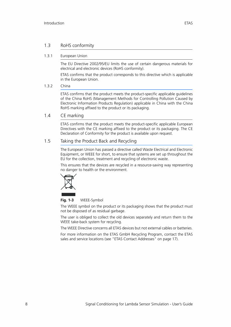
1.5 Taking the Product Back and Recycling
The European Union has passed a directive called Waste Electrical and ElectronicEquipment, or WEEE for short, to ensure that systems are set up throughout theEU for the collection, treatment and recycling of electronic waste.
This ensures that the devices are recycled in a resource-saving way representingno danger to health or the environment.
Fig. 1-3 WEEE-Symbol
The WEEE symbol on the product or its packaging shows that the product mustnot be disposed of as residual garbage.
The user is obliged to collect the old devices separately and return them to theWEEE take-back system for recycling.
The WEEE Directive concerns all ETAS devices but not external cables or batteries.
For more information on the ETAS GmbH Recycling Program, contact the ETASsales and service locations (see "ETAS Contact Addresses" on page 17).
Signal Conditioning for Lambda Sensor Simulation - User’s Guide
ETAS Hardware
2 Hardware
This chapter describes the assembly and configuration of the PB1652LAMBDA.1-C Signal Conditioning for Lambda Sensor Simulation.
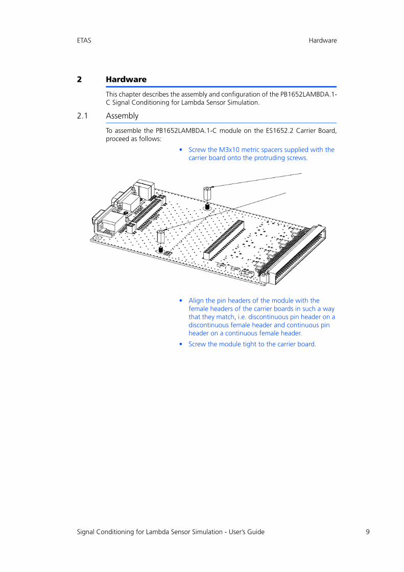
2.1 Assembly
To assemble the PB1652LAMBDA.1-C module on the ES1652.2 Carrier Board,proceed as follows:
• Screw the M3x10 metric spacers supplied with the carrier board onto the protruding screws.
• Align the pin headers of the module with the female headers of the carrier boards in such a way that they match, i.e. discontinuous pin header on a discontinuous female header and continuous pin header on a continuous female header.
• Screw the module tight to the carrier board.
Signal Conditioning for Lambda Sensor Simulation - User’s Guide 9
10
Hardware ETAS
2.2 Configuration
2.2.1 Jumpers for Ground Reference
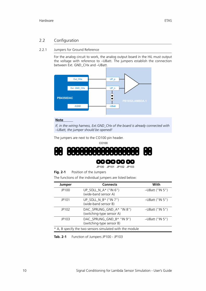
For the analog circuit to work, the analog output board in the HiL must outputthe voltage with reference to –UBatt. The jumpers establish the connectionbetween Ext. GND_CHx and –UBatt.
The jumpers are next to the CO100 pin header.
Fig. 2-1 Position of the Jumpers
The functions of the individual jumpers are listed below:
Tab. 2-1 Function of Jumpers JP100 - JP103
Note
If, in the wiring harness, Ext.GND_CHx of the board is already connected with –UBatt, the jumper should be opened!
Jumper Connects With
JP100 UP_SOLL_N_A* ("IN 6") (wide-band sensor A)
–UBatt ("IN 5")
JP101 UP_SOLL_N_B* ("IN 7")(wide-band sensor B)
–UBatt ("IN 5")
JP102 DAC_SPRUNG_GND_A* "IN 8")(switching-type sensor A)
–UBatt ("IN 5")
JP103 DAC_SPRUNG_GND_B* "IN 9")(switching-type sensor B)
–UBatt ("IN 5")
* A, B specify the two sensors simulated with the module
PB1652LAMBDA.1 PB4350DAC
Out_CHx
Ext. GND_CHx
AGND
UP_p
-UBatt
UP_n
JP101JP100 JP102 JP103
CO100
Signal Conditioning for Lambda Sensor Simulation - User’s Guide

ETAS Hardware
2.2.2 Relays for the Simulation of Wide-Band Sensors of the Type "LSU5.1"
For the simulation of wide-band sensors of the type "LSU5.1", relays on theboard have to be switched (see Fig. 1-2 on page 6). For this purpose, 12 V has tobe applied at Pin 15 ("RELAY_VCC") of the "OUT 1..15" port (see Tab. 3-2on page 14).
The relay for wide-band sensor A is switched when Pin 12 ("RELAY_LSW_A") isconnected with GND; the relay for wide-band sensor B is switched when Pin 11("RELAY_LSW_B") is connected with GND.
2.2.3 Configuration of Switching-Type Sensors
The resistors (200 Ohm) of the switching-type sensors are already present on themodules. External variable resistors can be used by setting the jumpers on theboard (P201/JP301 - see Fig. 2-2).
Fig. 2-2 Jumpers for the Resistors of a Switching-Type Sensor
LSF_A/B
SPRUNGSONDE_A/B
U_DAC_SPRUNG_A/B
100R
JP201 (A)JP301 (B)
100R
Signal Conditioning for Lambda Sensor Simulation - User’s Guide 11

12
Hardware ETAS
2.2.4 Integration of Lambda Sensor Simulation in LABCAR
The following figure shows an example of how to connect the lambda sensorsimulation to LABCAR.
Fig. 2-3 Connection to LABCAR
Note
The connections shown in red must be explicitly established!
BoB
ES1652.2
Out_CH09
Out_CH08
Out_CH06
Out_CH07
EC
U1
Out_CH04
ExtGND_CH04
Out_CH05
ExtGND_CH05
Out_CH06
ExtGND_CH06
Out_CH07
ExtGND_CH07
UN2
UN1
IA2
IP2
IP1
IA1
140
IA2
UN2
Res3-
Res3+
IP2
142
158
157
IA3
UN3
Res4-
Res4+
IP3
IA4
UN4
Res5-
Res5+
IP4
IP1
IA1
155
UN1
Res2-
Res2+
137
138
156
150
149
143
144
145
159
160
147
148
162
161
VM
VM
ES1385.1
Res4+ -
Res5+ -
Res3
+ -
Res2+ -
139
ExtGND_CH06
ExtGND_CH07141
IN 5-UBatt
LSF_A
SPRUNGSONDE_A
U_DAC_SPRUNG_AOUT 8
OUT 9
IN 3
OUT 7
LSF_B
SPRUNGSONDE_B
U_DAC_SPRUNG_BOUT 11
OUT 12
IN 4
OUT 10146
ExtGND_CH06
LSU_A
IP_A
IA_A
UN_A
UP_SOLL_P_A
OUT 2
UP_SOLL_N_A
OUT 1
OUT 3
IN 1
VM_AOUT 13
IN 6
ExtGND_CH07
LSU_B
IP_B
IA_B
UN_B
UP_SOLL_P_B
OUT 5
UP_SOLL_N_B
OUT 4
OUT 6
IN 2
IN 7
VM_BOUT 14
VM_A
VM_B
Lambda external86 1817
PB
4350D
AC
1 #2
Signal Conditioning for Lambda Sensor Simulation - User’s Guide
ETAS Pin Assignment and LEDs
3 Pin Assignment and LEDs
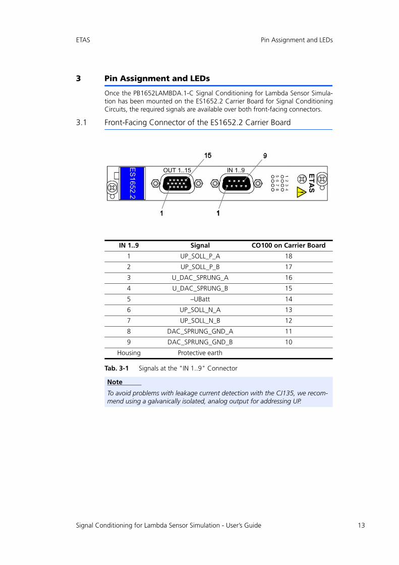
Once the PB1652LAMBDA.1-C Signal Conditioning for Lambda Sensor Simula-tion has been mounted on the ES1652.2 Carrier Board for Signal ConditioningCircuits, the required signals are available over both front-facing connectors.
3.1 Front-Facing Connector of the ES1652.2 Carrier Board
Tab. 3-1 Signals at the "IN 1..9" Connector
IN 1..9 Signal CO100 on Carrier Board
1 UP_SOLL_P_A 18
2 UP_SOLL_P_B 17
3 U_DAC_SPRUNG_A 16
4 U_DAC_SPRUNG_B 15
5 –UBatt 14
6 UP_SOLL_N_A 13
7 UP_SOLL_N_B 12
8 DAC_SPRUNG_GND_A 11
9 DAC_SPRUNG_GND_B 10
Housing Protective earth
Note
To avoid problems with leakage current detection with the CJ135, we recom-mend using a galvanically isolated, analog output for addressing UP.
Signal Conditioning for Lambda Sensor Simulation - User’s Guide 13

14
Pin Assignment and LEDs ETAS
Tab. 3-2 Signals at "OUT 1..15" Connector
3.2 LEDs
Fig. 3-1 LEDs on the Front Panel of the ES1652.2 Carrier Board
The yellow LEDs always light up when there is a module on the carrier board. Thered LEDs are not addressed by the PB1652LAMBDA.1-C.
OUT 1..15 Signal (Meaning) [ECU Pin] CO100 onCarrier Board
1 IP_A (pump current sensor A) [APE] 34
2 IA_A (compensating current sensor A) [MES] 33
3 UN_A (Nernst voltage sensor A) [RE] 32
4 IP_B (pump current sensor B) [APE] 31
5 IA_B (compensating current sensor B) [MES] 30
6 UN_B (Nernst voltage sensor B) [RE] 29
7 SPRUNGSONDE_A 28
8 n.c. 27
9 n.c. 26
10 SPRUNGSONDE_B 25
11 RELAY_LSW_B (see section 2.2.2 on page 11)
24
12 RELAY_LSW_A(see section 2.2.2 on page 11)
23
13 VM_A (virtual ground sensor A) [IPE] 22
14 VM_B (virtual ground sensor B) [IPE] 21
15 RELAY_VCC (see section 2.2.2 on page 11)
20
Housing Protective earth
1
5
2 3 4
6 7 8
Signal Conditioning for Lambda Sensor Simulation - User’s Guide

ETAS Technical Data
4 Technical Data
Analog Inputs
Analog Outputs
Supported Controllers
Environmental Conditions
4.1 Fulfilled Standards and Norms
The PB1652LAMBDA.1-C Signal Conditioning for Lambda Sensor Simulationcomplies with the following standards and norms:
Input voltage UP 0...5 V
Input current IP ±3 mA between IP and VM
Output voltage UN 0...1 V
Overvoltage protectionIP, IA, VM
±12 V for every channel
Usable with ES1652.1 and ES1652.2
Yes
CJ135STEP1 LSU4.x, LSF4.x, LSU5.1, ADV4.2, NTK ZFAS®
Operating temperature +5 °C to +50 °C (+41 °F to +122 °F)
Relative humidity 0 to 95% (non-condensing)
Storage temperature +5 °C to +85 °C (+41 °F to +185 °F)
Relative humidity 0 to 95% (non-condensing)
Norm Test
EN 61326-1 Electrical equipment for measurement, control and laboratory use – EMC requirements
EN 61000-6-2 Immunity (industrial environments)
EN 61000-6-3 Emission standard (residential, commercial andlight-industrial environments)
Note
The device confirms only with radio disturbances class A (only for industrial environment). This can cause radio disturbances in residen-tial, commercial and light industry environment. In such a case the operator has to consider additional measures for shielding to avoid disturbances.
Signal Conditioning for Lambda Sensor Simulation - User’s Guide 15
16
Technical Data ETAS
Signal Conditioning for Lambda Sensor Simulation - User’s Guide

ETAS ETAS Contact Addresses
5 ETAS Contact Addresses
ETAS HQ
ETAS GmbH
ETAS Subsidiaries and Technical Support
For details of your local sales office as well as your local technical support teamand product hotlines, take a look at the ETAS website:
Borsigstraße 14 Phone: +49 711 3423-0
70469 Stuttgart Fax: +49 711 3423-2106
Germany WWW: www.etas.com
ETAS subsidiaries WWW: www.etas.com/en/contact.php
ETAS technical support WWW: www.etas.com/en/hotlines.php
Signal Conditioning for Lambda Sensor Simulation - User’s Guide 17
18
ETAS Contact Addresses ETAS
Signal Conditioning for Lambda Sensor Simulation - User’s Guide

ETAS Index
Index
AAssembly 9BBlock diagram 6
CCE Declaration of Conformity 8Configuration 10Connector "IN 1..9" 13
EETAS Contact Addresses 17
FFeatures 5
JJumpers
for ground reference 10
LLEDs 14
PPort "OUT 1..15" 14Product Back 8
RRecycling 8
Relayssimulation of wide-band sensors
of the type "LSU5.1" 11RoHS conformity
China 8European Union 8
SSafety instructions, basic 7Safety instructions, labeling 7Standards and norms 15Switching-Type Sensor
Configuration 11
TTechnical data 15
UUse, correct 7Using with a carrier board 6
WWaste Electrical and Electronic Equip-
ment 8WEEE take-back system 8
Signal Conditioning for Lambda Sensor Simulation - User’s Guide 19

20
Index ETAS
Signal Conditioning for Lambda Sensor Simulation - User’s Guide