Embed Size (px)
Citation preview

Journal of Physics Conference Series
OPEN ACCESS
Sensing requirements for modern circuit boardinspectionTo cite this article D M Harvey et al 2007 J Phys Conf Ser 76 012010
View the article online for updates and enhancements
You may also likeApplication of the model of the printedcircuit board with regard to the topology ofexternal conductive layers for calculationof the thermal conditions of the printedcircuit boardI M Rybakov N V Goryachev I IKochegarov et al
-
Modal testing circuit board assembly of anelectronic apparatus by laser vibrometryV A Krasnoveikin I Yu Smolin N VDruzhinin et al
-
RGB representation of two-dimensionalmulti-spectral acoustic data for objectsurface profile imagingXinhua Guo Yuji Wada Yosuke Mizuno etal
-
This content was downloaded from IP address 2121072868 on 31012022 at 2311
Sensing requirements for modern circuit board inspection
D M Harvey1 G-Ming Zhang1 and D R Braden2
1 General Engineering Research Institute Liverpool John Moores University Byrom Street Liverpool L3 3AF UK 2 Delphi Delco Electronics Systems Kirkby Liverpool L33 7XL United Kingdom
E-mail dmharveyljmuacuk
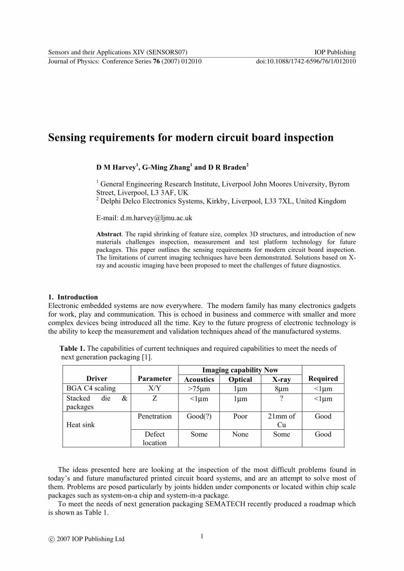
Abstract The rapid shrinking of feature size complex 3D structures and introduction of new materials challenges inspection measurement and test platform technology for future packages This paper outlines the sensing requirements for modern circuit board inspection The limitations of current imaging techniques have been demonstrated Solutions based on X-ray and acoustic imaging have been proposed to meet the challenges of future diagnostics
1 Introduction Electronic embedded systems are now everywhere The modern family has many electronics gadgets for work play and communication This is echoed in business and commerce with smaller and more complex devices being introduced all the time Key to the future progress of electronic technology is the ability to keep the measurement and validation techniques ahead of the manufactured systems Table 1 The capabilities of current techniques and required capabilities to meet the needs of next generation packaging [1]
Imaging capability Now Driver
Parameter Acoustics Optical X-ray
Required
BGA C4 scaling XY gt75microm 1microm 8microm lt1microm Stacked die amp packages
Z lt1microm 1microm lt1microm
Penetration Good() Poor 21mm of Cu
Good Heat sink
Defect location
Some None Some Good
The ideas presented here are looking at the inspection of the most difficult problems found in todayrsquos and future manufactured printed circuit board systems and are an attempt to solve most of them Problems are posed particularly by joints hidden under components or located within chip scale packages such as system-on-a chip and system-in-a package
To meet the needs of next generation packaging SEMATECH recently produced a roadmap which is shown as Table 1
Sensors and their Applications XIV (SENSORS07) IOP PublishingJournal of Physics Conference Series 76 (2007) 012010 doi1010881742-6596761012010
ccopy 2007 IOP Publishing Ltd 1
2 Sensing and measurement techniques for PCB inspection Equipment manufacturers are striving to meet the present and future needs for inspection based on four methods
1 X-ray has a high resolution down to a one micron spot size This gives good resolution in the
x-y plane but is limited in the Z direction as the X-rays only measure the density of the material they pass through X-rays are good for passing through objects such as heat sinks and multiple layer PCBs with only minor effects to the required image X-rays have been shown to detect solder bridges on 17x17mm 256 ball BGAs across two or more balls with the ability to detect voids with diameters 50 to 10 microns [2]
2 Optical Inspection can only see what we can see That is it can only detect surface images and analyse them Hidden bonds are out of bounds This type of inspection can be used to detect a raised leg on chips as small as 400 micron pitch using a 1696 x 1065 pixel camera [2]
3 Acoustic Inspection is very good for finding crack or air gap type defects such as delamination and dry joints Key to detection is in the signal processing since most acoustic images are shrouded in noise and need careful extraction of the meaningful signals [3]
4 Thermal Imaging can be active or passive In passive the PCB is powered as in normal operation and a thermal imaging camera simply looks at the heat signature of the components on the PCB Passive thermal imaging can detect a difference of 2˚C through a simple 640x480 pixel camera and see hot spots in components as small as 1x1mm [2]
No individual method of inspection can inspect all of the possible defects on manufactured PCBs so some form of combined sensing is required This could be an in-line system with individual inspection stations such as in the microscan project [2] or by combining two or more of the imaging systems using data fusion proposed recently by the authors
3 Measurements of manufactured circuit boards To detect hidden solder bonds or other artefacts X-ray and acoustic methods are the most accurate at present but still fall short for future applications It is unlikely that they will be able to inspect nanotechnology devices unless they can be improved significantly
(a) (b)
Figure 1 Inspection of an un-reflowed solder bump (a) X-ray image (b) acoustic image
Sensors and their Applications XIV (SENSORS07) IOP PublishingJournal of Physics Conference Series 76 (2007) 012010 doi1010881742-6596761012010
2
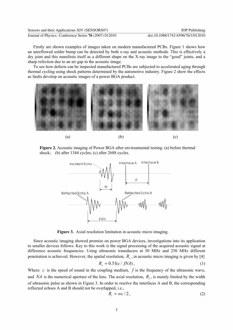
Firstly are shown examples of images taken on modern manufactured PCBs Figure 1 shows how an unreflowed solder bump can be detected by both x-ray and acoustic methods This is effectively a dry joint and this manifests itself as a different shape on the X-ray image to the ldquogoodrdquo joints and a sharp refection due to an air gap in the acoustic image
To see how defects can be inspected manufactured PCBs are subjected to accelerated aging through thermal cycling using shock patterns determined by the automotive industry Figure 2 show the effects as faults develop on acoustic images of a power BGA product
(a) (b) (c)
Since acoustic imaging showed promise on power BGA devices investigations into its application to smaller devices follows Key to this work is the signal processing of the acquired acoustic signal at difference acoustic frequencies Using ultrasonic transducers at 50 MHz and 250 MHz different penetration is achieved However the spatial resolution sR in acoustic micro imaging is given by [4]
)(510 fNAcRs = (1) Where c is the speed of sound in the coupling medium f is the frequency of the ultrasonic wave and NA is the numerical aperture of the lens The axial resolution tR is mainly limited by the width of ultrasonic pulse as shown in Figure 3 In order to resolve the interfaces A and B the corresponding reflected echoes A and B should not be overlapped ie
2wcRt = (2)
Figure 2 Acoustic imaging of Power BGA after environmental testing (a) before thermal shock (b) after 1344 cycles (c) after 2688 cycles
Figure 3 Axial resolution limitation in acoustic micro imaging
Sensors and their Applications XIV (SENSORS07) IOP PublishingJournal of Physics Conference Series 76 (2007) 012010 doi1010881742-6596761012010
3
Where w is the width of the ultrasonic pulse Obviously higher resolutions are obtained at the higher frequencies since the width w will be smaller Therefore a dilemma exists between the resolution and penetration since the best penetration into devices occurs at the lower frequencies
20 40 60 80 100 120 140
-50
0
50
100
time ns
ampl
itude
(a) AMI Signal 230MHz
time
frequ
ency
(b) Phase Plane
0 02 04 06 08 10
02
04
06
08
1
20 40 60 80 100 120 140
-50
0
50
time ns
ampl
itude
(c) AMI Signal 50MHz
time
frequ
ency
(d) Phase Plane
0 02 04 06 08 10
02
04
06
08
1
(a) (b)
This effect is further demonstrated in Figs 4 and 5 Fig 4a shows clear distinctions between the
reflected echoes from different layers on a circuit board using a 250MHz transducer Echo overlap has been observed in Fig 4c due to the lower resolution of a 50MHz transducer so that the echoes from
Figure 5 Acoustic C-scans of solder joints produced from the detection of a flip-chip package soldered on a ceramic substrate (a) Using 230MHz transducer (b) Using 50MHz transducer
Figure 4 Example A-scans from a circuit board acquired by (a) 230MHz transducer and (c) 50MHz transducer (b) The learning overcomplete representations of (a) (d) The learning overcomplete representations of (b)
Sensors and their Applications XIV (SENSORS07) IOP PublishingJournal of Physics Conference Series 76 (2007) 012010 doi1010881742-6596761012010
4
the interfaces of interest are distorted by the neighbouring echoes As a result the resulting C-scan image is contaminated which is clearly seen in Figure 5 Figure 5a shows a sharp image of the solder bonds from the 250MHz transducer whereas Figure 5b includes blurring caused by reflections from other layers
A solution which integrates modern signal processing techniques into conventional acoustic micro imaging techniques to improve the axial resolution without increasing the ultrasonic frequencies has been proposed recently by the authors [3] The ultrasonic A-scans were firstly decomposed into time-frequency domain using sparse signal representations The overlapped echoes are then separated in the transformation domain A time-frequency window is further used to select the interested interface echoes to generate a clean C-scan image This idea has been demonstrated in Fig 4 where the echoes in Fig 4c are overlapped in the time domain but are separated in the transformation domain as shown in Fig 4d thus producing a sharp C-scan image
4 Combined Solution It can be seen from Table 1 that different imaging approaches are only good at some of the required capabilities Each technology has distinct discriminating features and are good at inspecting for certain types of defect [5] AMI has a high axial resolution and is an effective approach for detecting gap-type defects such as voids delaminations disbond and thin cracks (sim01microm in the z-direction) due to the strong reflection of ultrasound in a solid-air interface These defects are difficult to find by X-ray inspection owing to low contrast On the other hand 2D X-ray inspection has a high lateral resolution but without axial resolving capability It is able to identify volumetric defects for example solder bridges and broken wires which are hard to detect by AMI Clearly X-ray inspection and AMI are complementary since AMI has high axial resolution but lower lateral resolution and X-rays have the opposite The author are developing a combined system would exploit the advantages of the two imaging techniques improving the reliability of defect detection and increasing the image contrast and resolution [5]
5 Conclusion We have reviewed the sensing requirements for next generation packages The preliminary results using X-ray and acoustic micro imaging techniques have been presented An advanced acoustic micro imaging technique has been demonstrated as a solution to improve the axial resolution of conventional acoustic micro imaging systems A combined acoustic and X-ray solution has been proposed for future devices
References [1] Dias R Goruganthu R Goyal D Hartfield C Hunt D McClelland D Cargo J Samuelson G
and Stierman R 2005 Assembly analytical forum analytical tool roadmap white paper International SEMATECH
[2] httpwwwmicroscaneucomprojectspr_3jsp [3] Zhang G-M Harvey D M and Braden D R 2005 Journal of the Acoustical Society of America
118 3706-3720 [4] Briggs G A D 1992 Acoustic Microscopy (Clarendon Oxford) p 33 [5] Harvey D M Burton D R and Zhang G-M 2007 Characterisation of future electronic packages
using advanced imaging techniques EPSRC proposal
Sensors and their Applications XIV (SENSORS07) IOP PublishingJournal of Physics Conference Series 76 (2007) 012010 doi1010881742-6596761012010
5
Sensing requirements for modern circuit board inspection
D M Harvey1 G-Ming Zhang1 and D R Braden2
1 General Engineering Research Institute Liverpool John Moores University Byrom Street Liverpool L3 3AF UK 2 Delphi Delco Electronics Systems Kirkby Liverpool L33 7XL United Kingdom
E-mail dmharveyljmuacuk
Abstract The rapid shrinking of feature size complex 3D structures and introduction of new materials challenges inspection measurement and test platform technology for future packages This paper outlines the sensing requirements for modern circuit board inspection The limitations of current imaging techniques have been demonstrated Solutions based on X-ray and acoustic imaging have been proposed to meet the challenges of future diagnostics
1 Introduction Electronic embedded systems are now everywhere The modern family has many electronics gadgets for work play and communication This is echoed in business and commerce with smaller and more complex devices being introduced all the time Key to the future progress of electronic technology is the ability to keep the measurement and validation techniques ahead of the manufactured systems Table 1 The capabilities of current techniques and required capabilities to meet the needs of next generation packaging [1]
Imaging capability Now Driver
Parameter Acoustics Optical X-ray
Required
BGA C4 scaling XY gt75microm 1microm 8microm lt1microm Stacked die amp packages
Z lt1microm 1microm lt1microm
Penetration Good() Poor 21mm of Cu
Good Heat sink
Defect location
Some None Some Good
The ideas presented here are looking at the inspection of the most difficult problems found in todayrsquos and future manufactured printed circuit board systems and are an attempt to solve most of them Problems are posed particularly by joints hidden under components or located within chip scale packages such as system-on-a chip and system-in-a package
To meet the needs of next generation packaging SEMATECH recently produced a roadmap which is shown as Table 1
Sensors and their Applications XIV (SENSORS07) IOP PublishingJournal of Physics Conference Series 76 (2007) 012010 doi1010881742-6596761012010
ccopy 2007 IOP Publishing Ltd 1
2 Sensing and measurement techniques for PCB inspection Equipment manufacturers are striving to meet the present and future needs for inspection based on four methods
1 X-ray has a high resolution down to a one micron spot size This gives good resolution in the
x-y plane but is limited in the Z direction as the X-rays only measure the density of the material they pass through X-rays are good for passing through objects such as heat sinks and multiple layer PCBs with only minor effects to the required image X-rays have been shown to detect solder bridges on 17x17mm 256 ball BGAs across two or more balls with the ability to detect voids with diameters 50 to 10 microns [2]
2 Optical Inspection can only see what we can see That is it can only detect surface images and analyse them Hidden bonds are out of bounds This type of inspection can be used to detect a raised leg on chips as small as 400 micron pitch using a 1696 x 1065 pixel camera [2]
3 Acoustic Inspection is very good for finding crack or air gap type defects such as delamination and dry joints Key to detection is in the signal processing since most acoustic images are shrouded in noise and need careful extraction of the meaningful signals [3]
4 Thermal Imaging can be active or passive In passive the PCB is powered as in normal operation and a thermal imaging camera simply looks at the heat signature of the components on the PCB Passive thermal imaging can detect a difference of 2˚C through a simple 640x480 pixel camera and see hot spots in components as small as 1x1mm [2]
No individual method of inspection can inspect all of the possible defects on manufactured PCBs so some form of combined sensing is required This could be an in-line system with individual inspection stations such as in the microscan project [2] or by combining two or more of the imaging systems using data fusion proposed recently by the authors
3 Measurements of manufactured circuit boards To detect hidden solder bonds or other artefacts X-ray and acoustic methods are the most accurate at present but still fall short for future applications It is unlikely that they will be able to inspect nanotechnology devices unless they can be improved significantly
(a) (b)
Figure 1 Inspection of an un-reflowed solder bump (a) X-ray image (b) acoustic image
Sensors and their Applications XIV (SENSORS07) IOP PublishingJournal of Physics Conference Series 76 (2007) 012010 doi1010881742-6596761012010
2
Firstly are shown examples of images taken on modern manufactured PCBs Figure 1 shows how an unreflowed solder bump can be detected by both x-ray and acoustic methods This is effectively a dry joint and this manifests itself as a different shape on the X-ray image to the ldquogoodrdquo joints and a sharp refection due to an air gap in the acoustic image
To see how defects can be inspected manufactured PCBs are subjected to accelerated aging through thermal cycling using shock patterns determined by the automotive industry Figure 2 show the effects as faults develop on acoustic images of a power BGA product
(a) (b) (c)
Since acoustic imaging showed promise on power BGA devices investigations into its application to smaller devices follows Key to this work is the signal processing of the acquired acoustic signal at difference acoustic frequencies Using ultrasonic transducers at 50 MHz and 250 MHz different penetration is achieved However the spatial resolution sR in acoustic micro imaging is given by [4]
)(510 fNAcRs = (1) Where c is the speed of sound in the coupling medium f is the frequency of the ultrasonic wave and NA is the numerical aperture of the lens The axial resolution tR is mainly limited by the width of ultrasonic pulse as shown in Figure 3 In order to resolve the interfaces A and B the corresponding reflected echoes A and B should not be overlapped ie
2wcRt = (2)
Figure 2 Acoustic imaging of Power BGA after environmental testing (a) before thermal shock (b) after 1344 cycles (c) after 2688 cycles
Figure 3 Axial resolution limitation in acoustic micro imaging
Sensors and their Applications XIV (SENSORS07) IOP PublishingJournal of Physics Conference Series 76 (2007) 012010 doi1010881742-6596761012010
3
Where w is the width of the ultrasonic pulse Obviously higher resolutions are obtained at the higher frequencies since the width w will be smaller Therefore a dilemma exists between the resolution and penetration since the best penetration into devices occurs at the lower frequencies
20 40 60 80 100 120 140
-50
0
50
100
time ns
ampl
itude
(a) AMI Signal 230MHz
time
frequ
ency
(b) Phase Plane
0 02 04 06 08 10
02
04
06
08
1
20 40 60 80 100 120 140
-50
0
50
time ns
ampl
itude
(c) AMI Signal 50MHz
time
frequ
ency
(d) Phase Plane
0 02 04 06 08 10
02
04
06
08
1
(a) (b)
This effect is further demonstrated in Figs 4 and 5 Fig 4a shows clear distinctions between the
reflected echoes from different layers on a circuit board using a 250MHz transducer Echo overlap has been observed in Fig 4c due to the lower resolution of a 50MHz transducer so that the echoes from
Figure 5 Acoustic C-scans of solder joints produced from the detection of a flip-chip package soldered on a ceramic substrate (a) Using 230MHz transducer (b) Using 50MHz transducer
Figure 4 Example A-scans from a circuit board acquired by (a) 230MHz transducer and (c) 50MHz transducer (b) The learning overcomplete representations of (a) (d) The learning overcomplete representations of (b)
Sensors and their Applications XIV (SENSORS07) IOP PublishingJournal of Physics Conference Series 76 (2007) 012010 doi1010881742-6596761012010
4
the interfaces of interest are distorted by the neighbouring echoes As a result the resulting C-scan image is contaminated which is clearly seen in Figure 5 Figure 5a shows a sharp image of the solder bonds from the 250MHz transducer whereas Figure 5b includes blurring caused by reflections from other layers
A solution which integrates modern signal processing techniques into conventional acoustic micro imaging techniques to improve the axial resolution without increasing the ultrasonic frequencies has been proposed recently by the authors [3] The ultrasonic A-scans were firstly decomposed into time-frequency domain using sparse signal representations The overlapped echoes are then separated in the transformation domain A time-frequency window is further used to select the interested interface echoes to generate a clean C-scan image This idea has been demonstrated in Fig 4 where the echoes in Fig 4c are overlapped in the time domain but are separated in the transformation domain as shown in Fig 4d thus producing a sharp C-scan image
4 Combined Solution It can be seen from Table 1 that different imaging approaches are only good at some of the required capabilities Each technology has distinct discriminating features and are good at inspecting for certain types of defect [5] AMI has a high axial resolution and is an effective approach for detecting gap-type defects such as voids delaminations disbond and thin cracks (sim01microm in the z-direction) due to the strong reflection of ultrasound in a solid-air interface These defects are difficult to find by X-ray inspection owing to low contrast On the other hand 2D X-ray inspection has a high lateral resolution but without axial resolving capability It is able to identify volumetric defects for example solder bridges and broken wires which are hard to detect by AMI Clearly X-ray inspection and AMI are complementary since AMI has high axial resolution but lower lateral resolution and X-rays have the opposite The author are developing a combined system would exploit the advantages of the two imaging techniques improving the reliability of defect detection and increasing the image contrast and resolution [5]
5 Conclusion We have reviewed the sensing requirements for next generation packages The preliminary results using X-ray and acoustic micro imaging techniques have been presented An advanced acoustic micro imaging technique has been demonstrated as a solution to improve the axial resolution of conventional acoustic micro imaging systems A combined acoustic and X-ray solution has been proposed for future devices
References [1] Dias R Goruganthu R Goyal D Hartfield C Hunt D McClelland D Cargo J Samuelson G
and Stierman R 2005 Assembly analytical forum analytical tool roadmap white paper International SEMATECH
[2] httpwwwmicroscaneucomprojectspr_3jsp [3] Zhang G-M Harvey D M and Braden D R 2005 Journal of the Acoustical Society of America
118 3706-3720 [4] Briggs G A D 1992 Acoustic Microscopy (Clarendon Oxford) p 33 [5] Harvey D M Burton D R and Zhang G-M 2007 Characterisation of future electronic packages
using advanced imaging techniques EPSRC proposal
Sensors and their Applications XIV (SENSORS07) IOP PublishingJournal of Physics Conference Series 76 (2007) 012010 doi1010881742-6596761012010
5