Embed Size (px)
Citation preview

Yau - 1SMT
EtchEtch

Yau - 2SMT
Objectives
After studying the material in this chapter, you will be able to:1. List and discuss eight important etch parameters.2. Explain dry etch, including its advantages and how etching
action takes place.3. List and describe the equipment systems for seven dry
plasma etch reactors.4. Explain the benefits of high-density plasma (HDP) etch and
the discuss the four types of HDP reactors.5. Give an application example for dielectric, silicon and metal
dry etch.6. Discuss wet etch and its applications.7. Explain how photoresist is removed.8. Discuss etch inspection and important quality measures.

Yau - 3SMT
Applications for Wafer Etch in CMOS Technology
Photoresistmask Film
to be etched
(a) Photoresist-patterned substrate (b) Substrate after etch
Photoresistmask Protected
film
Figure 16.1

Yau - 4SMT
Process Flow in a Wafer Fab
Implant
Diffusion
Test/Sort
Etch
Polish
PhotoCompleted wafer
Unpatternedwafer
Wafer startThin Films
Wafer fabrication (front-end)
Used with permission from Advanced Micro Devices
Figure 16.2

Yau - 5SMT
Etch Process
Categories of Etch Processes• Wet Etch• Dry Etch• Three Major Materials to be Etched
– Silicon– Dielectric– Metal
• Patterned Etch Versus Unpatterned Etch

Yau - 6SMT
Etch Parameters
• Etch rate• Etch profile• Etch bias• Selectivity• Uniformity• Residues• Polymer formation• Plasma-induced damage• Particle contamination and defects

Yau - 7SMT
Etch Rate
∆T
Start of etch End of etch
t = elapsed time during etch
∆T = change in thickness
Figure 16.3

Yau - 8SMT
Wet Chemical Isotropic Etch
Isotropic etch - etches in all directions at the same rate
Substrate
Film
Resist
Figure 16.4

Yau - 9SMT
Anisotropic Etch with Vertical Etch Profile
Anisotropic etch - etches in only one direction
Resist
Substrate
Film
Figure 16.5

Yau - 10SMT
Sidewall Profiles for Wet Etch Versus Dry Etch
Type of Etch Sidewall Profile Diagram
Wet Etch Isotropic
Isotropic(depending onequipment ¶meters)Anisotropic
(depending onequipment ¶meters)
Anisotropic –Taper
Dry Etch
Silicon Trench
Table 16.1

Yau - 11SMT
Etch Bias
(b)
Bias
Substrate
Resist
Film
(a)
Bias
Resist
FilmFilm
Substrate
Wb
Wa
Figure 16.6

Yau - 12SMT
Etching Undercut and Slope
Undercut
Substrate
Resist
FilmOveretch
Figure 16.7

Yau - 13SMT
Etch Selectivity
S = Ef
Er
Ef Nitride
Oxide
Er
Figure 16.8
Yau - 14SMT
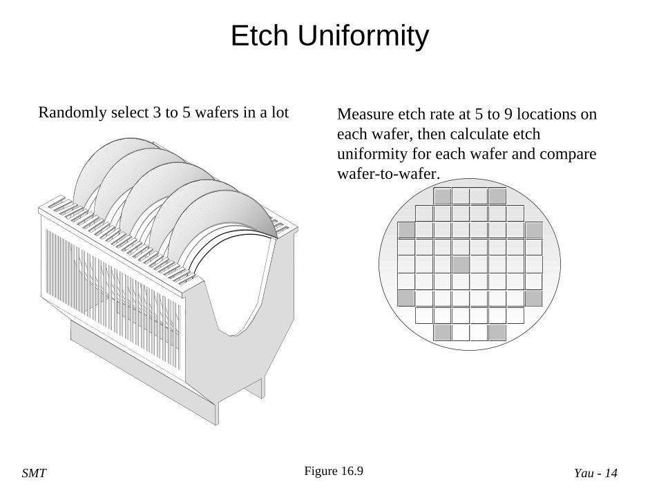
Etch Uniformity
Measure etch rate at 5 to 9 locations on each wafer, then calculate etch uniformity for each wafer and compare wafer-to-wafer.
Randomly select 3 to 5 wafers in a lot
Figure 16.9

Yau - 15SMT
Polymer Sidewall Passivation for Increased Anisotropy
Plasma ions
Resist
Oxide
Polymer formationSilicon
Figure 16.10

Yau - 16SMT
Dry Etch
• Advantages of Dry Etch over Wet Etch• Etching Action• Potential Distribution

Yau - 17SMT
Advantages of Dry Etch over Wet Etch
1. Etch profile is anisotropic with excellent control ofsidewall profiles.
2. Good CD control.
3. Minimal resist lifting or adhesion problems.
4. Good etch uniformity within wafer, wafer-to-waferand lot-to-lot.
5. Lower chemical costs for usage and disposal.
Table 16.2

Yau - 18SMT
Plasma Etch Process of a Silicon Wafer
8) By-product removal
1) Etchant gases enter chamber
Substrate
Etch process chamber
2) Dissociation of reactants by electric fields
5) Adsorption of reactive ions on surface
4) Reactive +ions bombard surface 6) Surface reactions of
radicals and surface film
Exhaust
Gas delivery
RF generator
By-products
3) Recombination of electrons with atoms creates plasma
7) Desorption of by-products
Cathode
AnodeElectric field
λ
λ
Anisotropic etch Isotropic etch
Figure 16.11

Yau - 19SMT
Chemical and Physical Dry Etch Mechanisms
Reactive +ions bombard surface Surface reactions of
radicals + surface film
Desorption of by-products
Anisotropic etch Isotropic etch
Sputtered surface material
Chemical EtchingPhysical Etching
Figure 16.12

Yau - 20SMT
Chemical Versus Physical Dry Plasma Etching
Etch Parameter
Physical Etch(RF field
perpendicularto wafersurface)
Physical Etch(RF field
parallel towafer surface)
Chemical EtchCombined
Physical andChemical
Etch Mechanism
Physical ionsputtering Radicals in
plasma reactingwith wafersurface*
Radicals inliquid reactingwith wafersurface
In dry etch,etching includesion sputteringand radicalsreacting withwafer surface
Sidewall Profile Anisotropic Isotropic Isotropic Isotropic toAnisotropic
SelectivityPoor/difficultto increase(1:1)
Fair/good (5:1to 100:1)
Good/excellent(up to 500:1)
Fair/good(5:1 to 100:1)
Etch Rate High Moderate Low Moderate
CD Control Fair/good Poor Poor to non-existent Good/excellent
* Used primarily for stripping and etchback operations.Table 16.3

Yau - 21SMT
Schematic View of Reactor Glow Discharge with Potential Distribution
Plasma (+Vp)Ion
sheath
RF
Powered electrode (Vt)
Grounded electrode
-V 0 +V
Vp
Vt
Figure 16.13

Yau - 22SMT
Effects of Changing Plasma Etch Parameters
Ion Energy DC Bias Etch Rate SelectivityPhysical
Etch
↑ ↓ ↓ ↓ ↑ ↓
↓ ↑ ↑ ↑ ↓ ↑
↑ ↑ ↑ ↑ ↓ ↑
↓ ↓ ↓ ↓ ↑ ↓
↑ ↑ ↑ ↑ ↓ ↑
↓ ↓ ↓ ↓ ↑ ↓
↑ ↓ ↓ ↓ ↑ ↓
↓ ↑ ↑ ↑ ↓ ↓
DC Bias
Electrical Size
Increase (↑) or Decrease (↓) in Etch Control Parameters
RF Frequency
RF Power
Table 16.4

Yau - 23SMT
Plasma Etch Reactors
• Barrel plasma etcher• Parallel plate (planar) reactor• Downstream etch systems• Triode planar reactor• Ion beam milling• Reactive ion etch (RIE)• High-density plasma etchers• Etch System Review• Endpoint Detection• Vacuum for Etch Chambers

Yau - 24SMT
Typical Barrel Reactor Configuration
Vacuum pump
Gas in
RF electrode
RFgenerator
Wafers
Quartz boat
Wafers
Reaction chamber
Figure 16.14

Yau - 25SMT
Parallel Plate Plasma Etching
Roots pump
Process gases
Exhaust
Gas- flow controller
Pressure controller
Gas panel
RF generatorMatching network
Microcontroller Operator Interface
Gas dispersion screen
Electrodes
Endpoint signal
Pressure signal
Roughingpump
Wafer
Figure 16.15
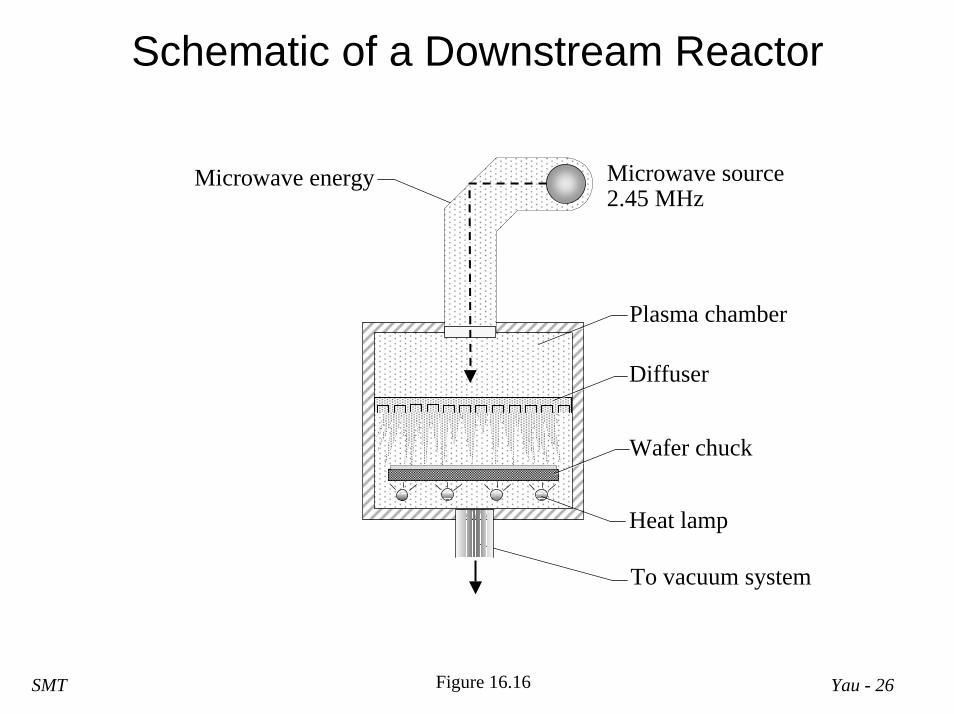
Yau - 26SMT
Schematic of a Downstream Reactor
Plasma chamber
Diffuser
Wafer chuck
Heat lamp
To vacuum system
Microwave energy Microwave source 2.45 MHz
Figure 16.16

Yau - 27SMT
Triode Planar Reactor
Inductively-coupledRF generator (3.56 MHz)
Capacitively-coupled RF generator (100 kHz)
Induction coil
Capacitor
Figure 16.17

Yau - 28SMT
General Schematic of Ion Beam Etcher
+
+
+
+
+
+
++
+
+
+
+
+
+++
+
+
+ ++
+ +
+
++
+
+
+
++ +
++
+
+
+
+
+
+
+
+
+
+
+
+
++
+
+
+
+
++
++ +
+ +_
Hot filament emits electrons
Gas inlet(Argon)
To vacuum system
Neutralizing filament
Accelerating gridScreen gridElectromagnet
improves ionization
Plasma chamber(+anode repels +ions)
Wafer can be tilted to control etch profile
Redrawn from Advanced Semiconductor Fabrication Handbook, Integrated Circuit Engineering Corp., p. 8-12.
Figure 16.18

Yau - 29SMT
Parallel Plate RIE Reactor
RF generator
Wafer
Powered electrode(cathode)
Grounded electrode
(anode)
Ar+
(physical etch component)
F(chemical etch
component)
Figure 16.19

Yau - 30SMT
High Density Plasma Etcher
Photograph courtesy of Applied Materials, Metal Etch DPS
Photo 16.1

Yau - 31SMT
Schematic of Electron Cyclotron ReactorMicrowave source 2.45 MHz
Wave guide
Diffuser
Quartz window
Electrostatic chuck
Cyclotron magnet
Plasma chamber
Wafer
Additional magnet
13.56 MHz
Vacuum systemRedrawn from Y. Lii, “Etching,” ULSI Technology, ed. by C. Chang & S. Sze, (New York: McGraw-Hill, 1996), p. 349.
Figure 16.20
Yau - 32SMT
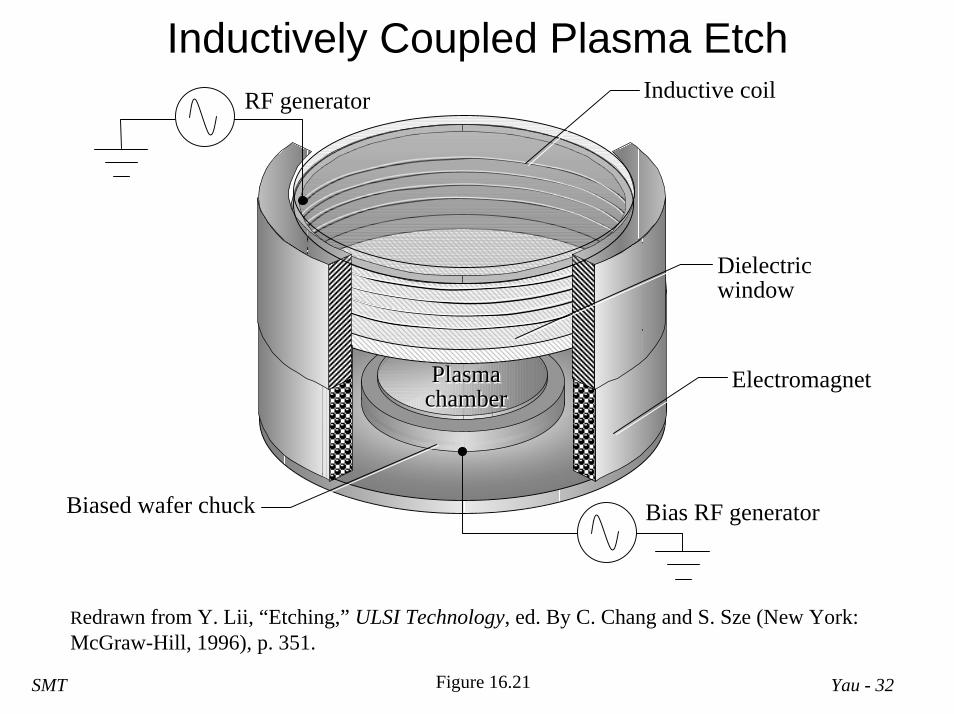
Inductively Coupled Plasma Etch
Electromagnet
Dielectric window
Inductive coil
Biased wafer chuck
RF generator
Bias RF generator
Plasma chamberPlasma
chamber
Redrawn from Y. Lii, “Etching,” ULSI Technology, ed. By C. Chang and S. Sze (New York: McGraw-Hill, 1996), p. 351.
Figure 16.21

Yau - 33SMT
Dual Plasma Source (DPS)
Decoupled plasma chamber
Decoupled plasma chamber
Turbo pump
Lower chamber
Cathode
Wafer
Capacitively-coupled RF generator (bias power)
Inductively-coupled RF generator (source power)
Redrawn from Y. Ye et al, Proceedings of Plasma Processing XI, vol. 96-12, ed. by G. Mathad and M. Meyyappan (Pennington, NJ: The Electrochemical Society, 1996), p. 222.
Figure 16.22

Yau - 34SMT
Magnetically Enhanced Reactive Ion Etch (MERIE)
Electromagnet (1 of 4)
13.56 MHz
Biased wafer chuck
WaferWafer
Redrawn from Wet/Dry Etch (College Station, TX: Texas Engineering Extension Service, 1996), p. 165.
Figure 16.23

Yau - 35SMT
Dry Etcher ConfigurationsConfigurations Activity Pressure
(Torr) ArrangementHigh
DensityPlasma
Biasing BiasSource Profile
Barrel Reactive 10-1 to 1 Coil or electrodes outsidevessel No In cassette (bulk) RF Isotropic
Parallel Plate (Plasma) Reactive 10-1 to 1 Planar diode (two electrodes) No On poweredelectrode (anode) RF Anisotropic
Downstream Plasma Reactive 10-1 to 1 Coil or electrodes outsidevessel No
In cassette (bulk)downstream ofplasma
RF orMicrowave Isotropic
Triode Planar Reactive 10-3 Triode (three electrodes) No On platformelectrode Anisotropic
Ion Beam Milling Inert 10-4 Planar triode No On poweredelectrode (anode) Anisotropic
Reactive Ion Etch(RIE) Reactive < 0.1 Planar or cylindrical diode No On cathode Anisotropic
Electron CyclotronResonance (ECR) Reactive
10-4 to 10-
3
(low)
Magnetic field in parallel withplasma flow Yes On cathode RF or DC Anisotropic
Distributed ECR Reactive (low) Magnets distributed aroundcentral plasma Yes On cathode RF or DC Anisotropic
Inductively CoupledPlasma (ICP) Reactive (low) Spiral coil separated from
plasma by dielectric plate Yes On cathode RF or DC Anisotropic
Helicon Wave Reactive (low)
Plasma generated byelectromagnets and plasmadensity maintained at wafer bymagnetic field
Yes On cathode RF or DC Anisotropic
Dual Plasma Source Reactive (low) Independent plasma and waferbiasing Yes On cathode RF or DC Anisotropic
MagneticallyEnhanced RIE(MERIE)
Reactive (low) Planar diode with magneticfield confining plasma Yes On cathode RF or DC Anisotropic
Table 16.5

Yau - 36SMT
Endpoint Detection for Plasma Etching
Endpoint detection
Normal etch Change in etch rate - detection occurs here.
Endpoint signal stops the etch.
Time
Etch
Par
amet
er
Figure 16.24

Yau - 37SMT
Characteristic Wavelengths of Excited Species in Plasma Etch
Material Etchant Gas Emitting Species ofsome Products Wavelength (nm)
SiliconCF4/O2
Cl2
SiFSiCl
440; 777287
SiO2 CHF3 CO 484
AluminumCl2
BCl3
AlAlCl
391; 394; 396261
PhotoresistO2 CO
OHH
484309656
Nitrogen(indicatingchamber vacuumleak)
N2
NO337248
Table 16.6

Yau - 38SMT
Endpoint Detection
Photograph courtesy of Advanced Micro Devices, Lam Rainbow etcher

Yau - 39SMT
Dry Etch Applications
• Dielectric Dry Etch– Oxide– Silicon Nitride
• Silicon Dry Etch– Polysilicon– Single-Crystal Silicon
• Metal Dry Etch– Aluminum and Metal
Stacks– Tungsten Etchback– Contact Metal Etch

Yau - 40SMT
Requirements for Successful Dry Etch
1. High selectivity to avoid etching materials that are not to be etched (primarily photoresist and underlying materials).
2. Fast etch rate to achieve an acceptable throughput of wafers.
3. Good sidewall profile control.4. Good etch uniformity across the wafer.5. Low device damage.6. Wide process latitude for manufacturing.

Yau - 41SMT
Dry Etch Critical Parameters
Equipment Parameters:• Equipment design• Source power• Source frequency• Pressure• Temperature• Gas-flow rate• Vacuum conditions• Process recipe
Other Contributing Factors:• Cleanroom protocol• Operating procedures• Maintenance procedures• Preventive maintenance schedule
Process Parameters:• Plasma-surface
interaction: - Surface material- Material stack of
different layers- Surface temperature- Surface charge- Surface topography
• Chemical and physical requirements
• Time
Quality Measures:• Etch rate• Selectivity• Uniformity• Feature profile• Critical dimensions• Residue
Plasma-etchinga wafer
Figure 16.25

Yau - 42SMT
Oxide Etch Reactor
CF4
C3F8
C4F8
CHF3
NF3
SiF4
ArWafer
Electrostatic chuck
Plasma
Selection of fluorocarbon and hydrocarbon chemicals
HF CF2
F
CHF
CH4
Figure 16.26

Yau - 43SMT
Etch Stop Hard Mask Layer
n-well p-well
LI Oxide
p+ Silicon Substrate
p- Epitaxial Layer
2 Doped oxide CVD
Nitride etch
5
Oxide CMP 3 4 Oxide etch1 Nitride CVD
Example: Silicon nitride, Si3N4, serves as etch-stop during LI oxide etch. Note: The numbers show the order of the five operations.
Figure 16.27

Yau - 44SMT
Contact Etching to Varying Depths
Contact holes
S DG
Figure 16.28

Yau - 45SMT
Polysilicon Conductor Length
Polysilicon gate Gate oxide
The gate length determines channel length and defines boundaries for source and drain electrodes.
DrainSource
Gate
Figure 16.29

Yau - 46SMT
Polysilicon Gate Etch Process Steps
1. Breakthrough step to remove native oxide and surface contaminants
2. Main-etch step to remove most polysiliconwithout damage to gate oxide
3. Overetch step to remove remaining residues and poly stringers while maintaining high selectivity to gate oxide

Yau - 47SMT
Undesirable Microtrenching duringPolysilicon Gate Etching
Substrate
Poly
Resist
Gate oxide
Ions
Trench in gate oxide
Figure 16.30

Yau - 48SMT
Silicon Trench Etching
Figure 16.31

Yau - 49SMT
Major Requirements for Metal Etching
1. High etch rates (>1000 nm/min).2. High selectivity to the masking layer (>4:1),
interlayer dielectric (>20:1) and to underlying layers.3. High uniformity with excellent CD control and no
microloading (<8% at any location on the wafer).4. No device damage from plasma-induced electrical
charging.5. Low residue contamination (e.g., copper residue,
developer attack and surface defects).6. Fast resist strip, often in a dedicated cluster tool
chamber, with no residual contamination.7. No corrosion.

Yau - 50SMT
Metal Stack for VLSI/ULSI Integration
TiN Al + Cu (1%)Ti
p+ Silicon substrate
p- Epitaxial layer
n-well p-well
LI Oxide
ILD-1
Metal etchPhotoresist mask
Figure 16.32
Yau - 51SMT
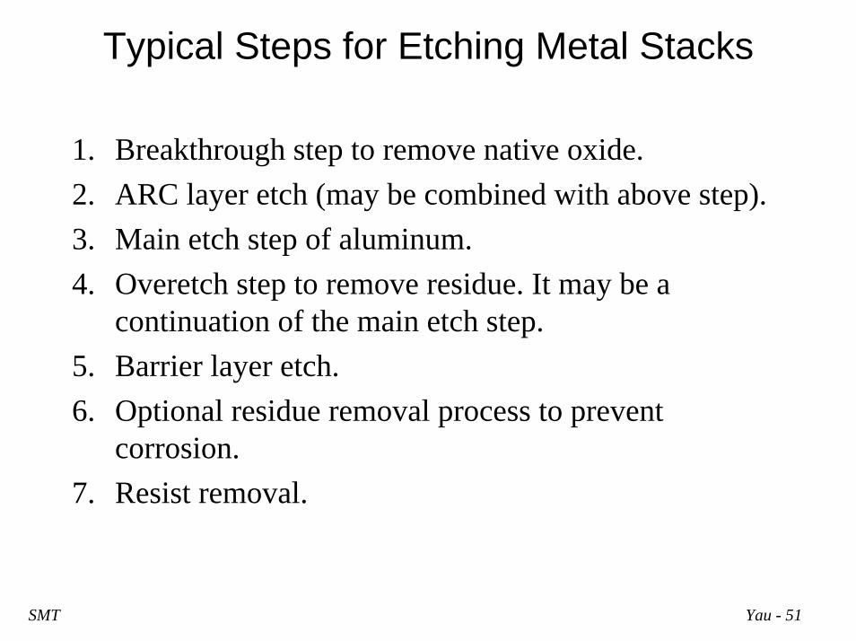
Typical Steps for Etching Metal Stacks
1. Breakthrough step to remove native oxide.2. ARC layer etch (may be combined with above step).3. Main etch step of aluminum.4. Overetch step to remove residue. It may be a
continuation of the main etch step.5. Barrier layer etch.6. Optional residue removal process to prevent
corrosion.7. Resist removal.

Yau - 52SMT
Tungsten Etchback
Metal-2 stack
(d) Metal-2 deposition
Tungstenplug
(a) Via etch through ILD-2 (SiO2)
Metal-1 stackILD-2
ILD-1
Via SiO2
(c) Tungsten etchback
SiO2Tungstenplug
(b) Tungsten CVD via fill
Tungsten
Figure 16.33

Yau - 53SMT
Wet Etch
• Wet Etch Parameters• Types of Wet Etch
– Wet Oxide Etch– Wet Chemical Strips

Yau - 54SMT
Wet Etch Parameters
Parameter Explanation Difficulty to Control
ConcentrationSolution concentration(e.g., ratio of NH4F:HFfor etch an oxide).
Most difficult parameter tocontrol because the bath
concentration is continuallychanging.
TimeTime of waferimmersion in the wetchemical bath.
Relatively easy to control.
Temperature Temperature of wetchemical bath. Relatively easy to control.
Agitation Agitation of the solutionbath.
Moderate difficulty toproperly control.
Table 16.7

Yau - 55SMT
Approximate Oxide Etch Rates in BHF Solution at 25° C
Table 16.81 Approximate Oxide Etch Rates in BHF Solution at 25°Ca
Type of Oxide Density (g/cm3) Etch Rate (nm/s)Dry grown 2.24 – 2.27 1Wet grown 2.18 – 2.21 1.5
CVD deposited < 2.00 1.5b – 5c
Sputtered < 2.00 10 – 20a) 10 parts of 454 g NH4F in 680 ml H2O and one part 48% HFb) Annealed at approximately 1000°C for 10 minutesc) Not annealed
1 B. El-Kareh, ibid, p. 277.
Table 16.8

Yau - 56SMT
Historical Perspective -Polysilicon Etch Technology Evolution
GeometryRequirements
Time Frameand Reactor
DesignChemistries Strengths Limitations and
Problems Controls
4 to 5 µm,isotropic etch
Pre-1977: wetetch
HF/HNO3buffered withacetic acid or H2O
Batch Process Resist lift; bath aging;temperature sensitive
Operator judgementfor endpoint
3 µm1977: barreletcher
CF4/O2 Batch Process Non-uniformity,isotropic etch, largeundercut
Manometer andtimer
2 µm
1981: singlewafer etch
CF4/O2 Single wafer; individualetch endpoint,improvement inrepeatability
Low oxide selectivity;isotropic process
Endpoint detection
1.5 µm
1982: singlewafer RIE
SF6/Freon 11,SF6/He
MFCs; independentpressure and gas flowcontrol, improvement inrepeatability
Low oxide selectivity;profile control
MFCs; separate gasflow and pressurecontrol
To 0.5 µm1983: variablegap; load-locked
CCl4/He, Cl2/He,Cl2/HBr
Load-locked chamber;variable gap, improvementin repeatability
Microloading in highaspect ratios; profilecontrol
Control ofelectrode gap;computer controls
To 0.25 µmand below
1991:inductivelycoupledplasma (ICP)
Cl2, HBr High-density plasma; lowpressure; simple gasmixtures, improvement inrepeatability
Complex tool; manyvariables
Independent RFcontrol for plasmageneration andwafer bias
Table 16.9

Yau - 57SMT
Photoresist Removal
Plasma Ashing• Asher Overview• Plasma Damage• Residue Removal

Yau - 58SMT
Atomic Oxygen Reaction with Resist in Asher
SubstrateResist
Asher reaction chamber
2) O2 dissociates into atomic oxygen 3) Plasma energy
turns oxygen into + ions
4) Neutral O and O+ react with C and H atoms in resist
Neutral oxygen radicals 5) By-product
desorption
6) By-product removal
Exhaust
Gas delivery
Downstream Plasma
1) O2 molecules enter chamber
+
++
++
++
λλ
+
Figure 16.34
Yau - 59SMT
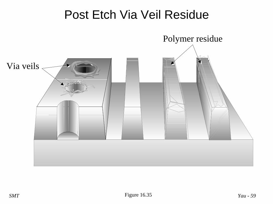
Post Etch Via Veil Residue
Via veils
Polymer residue
Figure 16.35