Embed Size (px)
Citation preview
2B1
1B1
2A
1A
S0
S1
1OE
2OE
1B2
1B3
1B4
2B2
2B3
2B4
SW
SW
SW
SW
SW
SW
SW
SW
7
9
14
2
1
15
6
5
4
3
10
11
12
13
Product
Folder
Sample &Buy
Technical
Documents
Tools &
Software
Support &Community
SN74CB3Q3253SCDS145B –OCTOBER 2003–REVISED JUNE 2015
SN74CB3Q3253 Dual 1-of-4 FET Multiplexer – Demultiplexer2.5-V – 3.3-V Low-Voltage High-Bandwidth Bus Switch
1 Features 3 DescriptionThe SN74CB3Q3253 device is a high-bandwidth FET
1• High-Bandwidth Data Path (Up to 500 MHz)bus switch using a charge pump to elevate the gate• 5-V Tolerant I/Os With Device Powered Up or voltage of the pass transistor, providing a low and flat
Powered Down ON-state resistance (ron). The low and flat ON-state• Low and Flat ON-State Resistance (ron) resistance allows for minimal propagation delay and
supports rail-to-rail switching on the data input andCharacteristics Over Operating Rangeoutput (I/O) ports.(ron = 4 Ω Typical)
• Rail-to-Rail Switching on Data I/O Ports Device Information– 0- to 5-V Switching With 3.3-V VCC ORDER NUMBER PACKAGE BODY SIZE (NOM)– 0- to 3.3-V Switching With 2.5-V VCC SN74CB3Q3253DBQ SSOP (16) 4.90 mm × 3.90 mm
• Bidirectional Data Flow With Near-Zero SN74CB3Q3253DGV TVSOP (16) 3.60 mm × 4.40 mmPropagation Delay SN74CB3Q3253RGY VQFN (16) 4.00 mm × 3.50 mm
• Low Input/Output Capacitance Minimizes Loading SN74CB3Q3253PW TSSOP (16) 5.00 mm × 4.40 mmand Signal Distortion (Cio(OFF) = 3.5 pF Typical)
(1) For all available packages, see the orderable addendum at• Fast Switching Frequency (fOE = 20 MHz Max) the end of the data sheet.• Data and Control Inputs Provide Undershoot
Logic Diagram (Positive Logic)Clamp Diodes• Low Power Consumption (ICC = 0.6 mA Typical)• VCC Operating Range From 2.3 V to 3.6 V• Data I/Os Support 0- to 5-V Signal Levels (0.8-V,
1.2-V, 1.5-V, 1.8-V, 2.5-V, 3.3-V, 5-V)• Control Inputs Can be Driven by TTL or 5-V and
3.3-V CMOS Outputs• Ioff Supports Partial-Power-Down Mode Operation• Latch-Up Performance Exceeds 100 mA Per
JESD 78, Class II• ESD Performance Tested Per JESD 22
– 2000-V Human-Body Model (A114-B, Class II)– 1000-V Charged-Device Model (C101)
• Supports Both Digital and Analog Applications:USB Interface, Differential Signal Interface BusIsolation, Low-Distortion Signal Gating
(1) For additional information regarding the performancecharacteristics of the CB3Q family, refer to the TI applicationreport CBT-C, CB3T, and CB3Q Signal-Switch Families,(SCDA008).
2 Applications• Video Broadcasting: IP-Based Multi-Format
Transcoder• Video Communications System
1
An IMPORTANT NOTICE at the end of this data sheet addresses availability, warranty, changes, use in safety-critical applications,intellectual property matters and other important disclaimers. PRODUCTION DATA.
SN74CB3Q3253SCDS145B –OCTOBER 2003–REVISED JUNE 2015 www.ti.com
Table of Contents8.3 Feature Description................................................... 91 Features .................................................................. 18.4 Device Functional Modes.......................................... 92 Applications ........................................................... 1
9 Application and Implementation ........................ 103 Description ............................................................. 19.1 Application Information............................................ 104 Revision History..................................................... 29.2 Typical Application ................................................. 105 Pin Configuration and Functions ......................... 3
10 Power Supply Recommendations ..................... 116 Specifications......................................................... 411 Layout................................................................... 116.1 Absolute Maximum Ratings ..................................... 4
11.1 Layout Guidelines ................................................. 116.2 ESD Ratings.............................................................. 411.2 Layout Example .................................................... 126.3 Recommended Operating Conditions....................... 4
12 Device and Documentation Support ................. 126.4 Thermal Information .................................................. 412.1 Documentation Support ........................................ 126.5 Electrical Characteristics .......................................... 512.2 Community Resources.......................................... 126.6 Switching Characteristics .......................................... 512.3 Trademarks ........................................................... 126.7 Typical Characteristics .............................................. 612.4 Electrostatic Discharge Caution............................ 127 Parameter Measurement Information .................. 712.5 Glossary ................................................................ 128 Detailed Description .............................................. 8
13 Mechanical, Packaging, and Orderable8.1 Overview ................................................................... 8Information ........................................................... 128.2 Functional Block Diagram ......................................... 9
4 Revision History
Changes from Revision A (November 2003) to Revision B Page
• Removed Ordering Information table. .................................................................................................................................... 1• Added Applications, Device Information table, Pin Configuration and Functions section, Storage Conditions table,
ESD Ratings table, Feature Description section, Device Functional Modes, Application and Implementation section,Power Supply Recommendations section, Layout section, Device and Documentation Support section, andMechanical, Packaging, and Orderable Information section ................................................................................................. 1
2 Submit Documentation Feedback Copyright © 2003–2015, Texas Instruments Incorporated
Product Folder Links: SN74CB3Q3253
1 16
8 9
2
3
4
5
6
7
15
14
13
12
11
10
2OE
S0
2B4
2B3
2B2
2B1
S1
1B4
1B3
1B2
1B1
1A
1O
E
2A
V
GN
D
CC
1
2
3
4
5
6
7
8
16
15
14
13
12
11
10
9
1OE
S1
1B4
1B3
1B2
1B1
1A
GND
VCC
2OE
S0
2B4
2B3
2B2
2B1
2A
SN74CB3Q3253www.ti.com SCDS145B –OCTOBER 2003–REVISED JUNE 2015
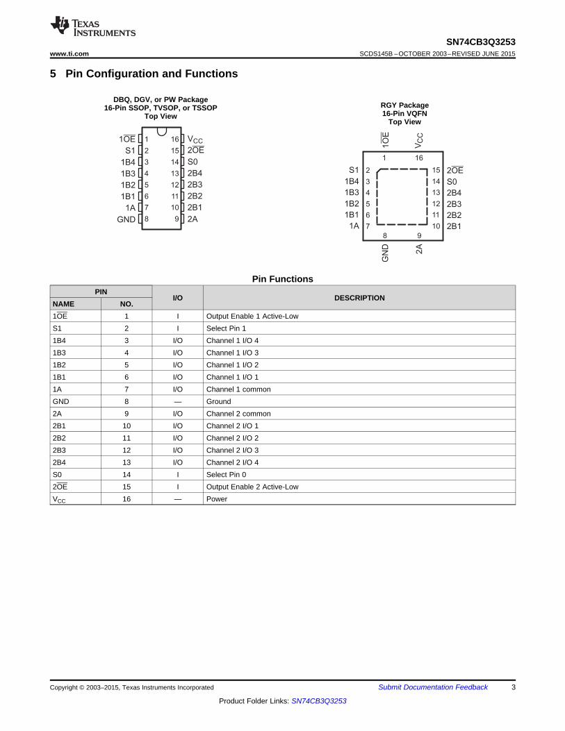
5 Pin Configuration and Functions
DBQ, DGV, or PW PackageRGY Package16-Pin SSOP, TVSOP, or TSSOP16-Pin VQFNTop View
Top View
Pin FunctionsPIN
I/O DESCRIPTIONNAME NO.1OE 1 I Output Enable 1 Active-LowS1 2 I Select Pin 11B4 3 I/O Channel 1 I/O 41B3 4 I/O Channel 1 I/O 31B2 5 I/O Channel 1 I/O 21B1 6 I/O Channel 1 I/O 11A 7 I/O Channel 1 commonGND 8 — Ground2A 9 I/O Channel 2 common2B1 10 I/O Channel 2 I/O 12B2 11 I/O Channel 2 I/O 22B3 12 I/O Channel 2 I/O 32B4 13 I/O Channel 2 I/O 4S0 14 I Select Pin 02OE 15 I Output Enable 2 Active-LowVCC 16 — Power
Copyright © 2003–2015, Texas Instruments Incorporated Submit Documentation Feedback 3
Product Folder Links: SN74CB3Q3253
SN74CB3Q3253SCDS145B –OCTOBER 2003–REVISED JUNE 2015 www.ti.com
6 Specifications
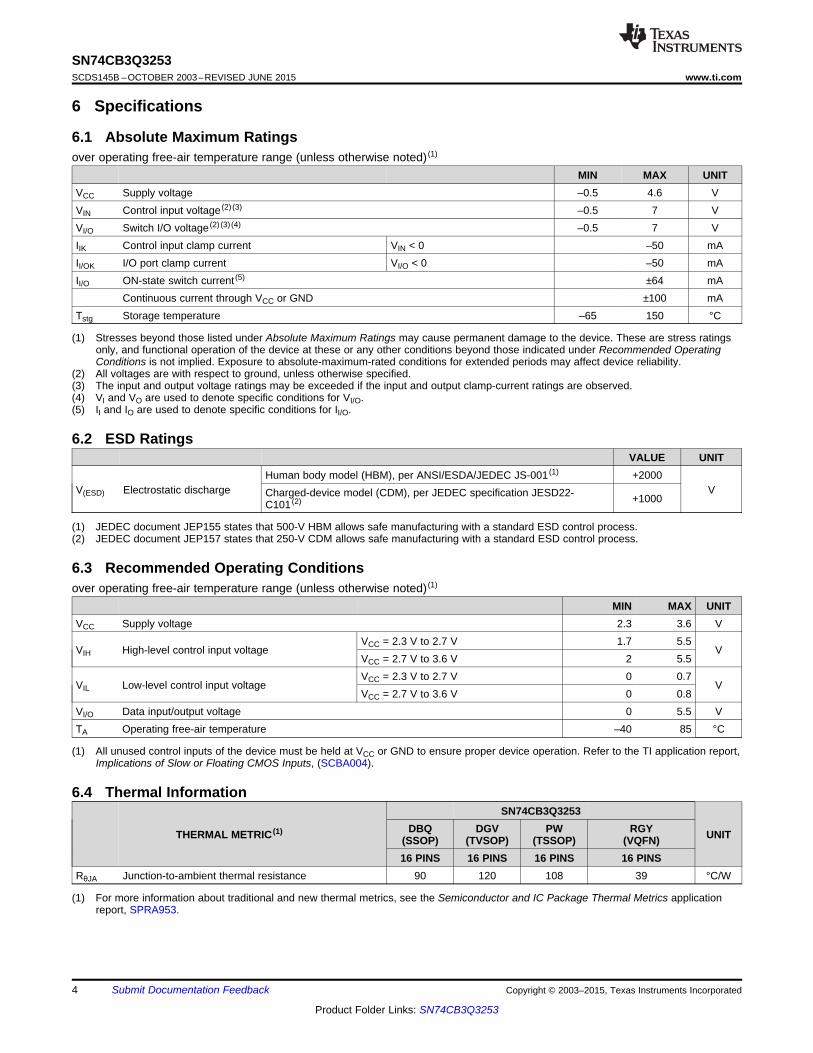
6.1 Absolute Maximum Ratingsover operating free-air temperature range (unless otherwise noted) (1)
MIN MAX UNITVCC Supply voltage –0.5 4.6 VVIN Control input voltage (2) (3) –0.5 7 VVI/O Switch I/O voltage (2) (3) (4) –0.5 7 VIIK Control input clamp current VIN < 0 –50 mAII/OK I/O port clamp current VI/O < 0 –50 mAII/O ON-state switch current (5) ±64 mA
Continuous current through VCC or GND ±100 mATstg Storage temperature –65 150 °C
(1) Stresses beyond those listed under Absolute Maximum Ratings may cause permanent damage to the device. These are stress ratingsonly, and functional operation of the device at these or any other conditions beyond those indicated under Recommended OperatingConditions is not implied. Exposure to absolute-maximum-rated conditions for extended periods may affect device reliability.
(2) All voltages are with respect to ground, unless otherwise specified.(3) The input and output voltage ratings may be exceeded if the input and output clamp-current ratings are observed.(4) VI and VO are used to denote specific conditions for VI/O.(5) II and IO are used to denote specific conditions for II/O.
6.2 ESD RatingsVALUE UNIT
Human body model (HBM), per ANSI/ESDA/JEDEC JS-001 (1) +2000V(ESD) Electrostatic discharge VCharged-device model (CDM), per JEDEC specification JESD22- +1000C101 (2)
(1) JEDEC document JEP155 states that 500-V HBM allows safe manufacturing with a standard ESD control process.(2) JEDEC document JEP157 states that 250-V CDM allows safe manufacturing with a standard ESD control process.
6.3 Recommended Operating Conditionsover operating free-air temperature range (unless otherwise noted) (1)
MIN MAX UNITVCC Supply voltage 2.3 3.6 V
VCC = 2.3 V to 2.7 V 1.7 5.5VIH High-level control input voltage V
VCC = 2.7 V to 3.6 V 2 5.5VCC = 2.3 V to 2.7 V 0 0.7
VIL Low-level control input voltage VVCC = 2.7 V to 3.6 V 0 0.8
VI/O Data input/output voltage 0 5.5 VTA Operating free-air temperature –40 85 °C
(1) All unused control inputs of the device must be held at VCC or GND to ensure proper device operation. Refer to the TI application report,Implications of Slow or Floating CMOS Inputs, (SCBA004).
6.4 Thermal InformationSN74CB3Q3253
DBQ DGV PW RGYTHERMAL METRIC (1) UNIT(SSOP) (TVSOP) (TSSOP) (VQFN)16 PINS 16 PINS 16 PINS 16 PINS
RθJA Junction-to-ambient thermal resistance 90 120 108 39 °C/W
(1) For more information about traditional and new thermal metrics, see the Semiconductor and IC Package Thermal Metrics applicationreport, SPRA953.
4 Submit Documentation Feedback Copyright © 2003–2015, Texas Instruments Incorporated
Product Folder Links: SN74CB3Q3253
SN74CB3Q3253www.ti.com SCDS145B –OCTOBER 2003–REVISED JUNE 2015
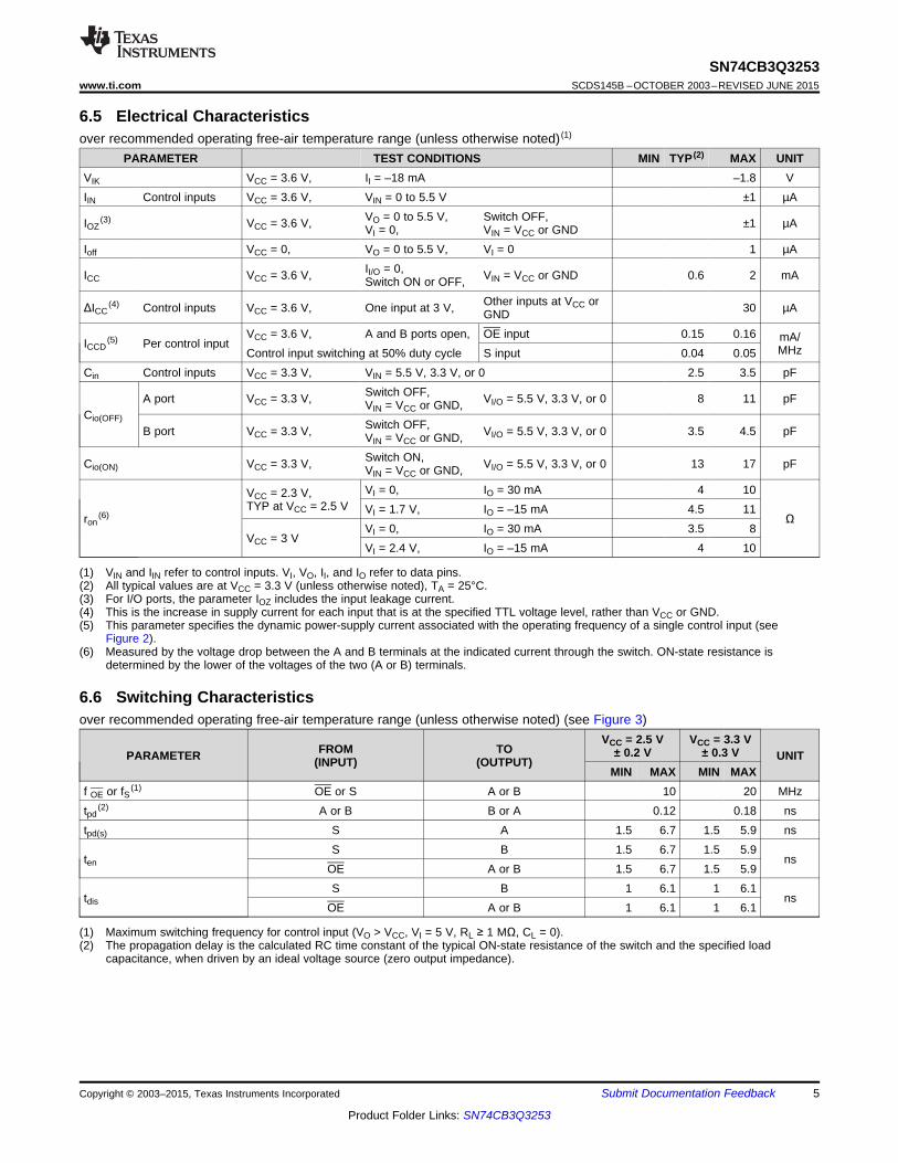
6.5 Electrical Characteristicsover recommended operating free-air temperature range (unless otherwise noted) (1)
PARAMETER TEST CONDITIONS MIN TYP (2) MAX UNITVIK VCC = 3.6 V, II = –18 mA –1.8 VIIN Control inputs VCC = 3.6 V, VIN = 0 to 5.5 V ±1 µA
VO = 0 to 5.5 V, Switch OFF,IOZ(3) VCC = 3.6 V, ±1 µAVI = 0, VIN = VCC or GND
Ioff VCC = 0, VO = 0 to 5.5 V, VI = 0 1 µAII/O = 0,ICC VCC = 3.6 V, VIN = VCC or GND 0.6 2 mASwitch ON or OFF,
Other inputs at VCC orΔICC(4) Control inputs VCC = 3.6 V, One input at 3 V, 30 µAGND
VCC = 3.6 V, A and B ports open, OE input 0.15 0.16 mA/ICCD(5) Per control input MHzControl input switching at 50% duty cycle S input 0.04 0.05
Cin Control inputs VCC = 3.3 V, VIN = 5.5 V, 3.3 V, or 0 2.5 3.5 pFSwitch OFF,A port VCC = 3.3 V, VI/O = 5.5 V, 3.3 V, or 0 8 11 pFVIN = VCC or GND,
Cio(OFF) Switch OFF,B port VCC = 3.3 V, VI/O = 5.5 V, 3.3 V, or 0 3.5 4.5 pFVIN = VCC or GND,Switch ON,Cio(ON) VCC = 3.3 V, VI/O = 5.5 V, 3.3 V, or 0 13 17 pFVIN = VCC or GND,VI = 0, IO = 30 mA 4 10VCC = 2.3 V,
TYP at VCC = 2.5 V VI = 1.7 V, IO = –15 mA 4.5 11ron
(6) ΩVI = 0, IO = 30 mA 3.5 8
VCC = 3 VVI = 2.4 V, IO = –15 mA 4 10
(1) VIN and IIN refer to control inputs. VI, VO, II, and IO refer to data pins.(2) All typical values are at VCC = 3.3 V (unless otherwise noted), TA = 25°C.(3) For I/O ports, the parameter IOZ includes the input leakage current.(4) This is the increase in supply current for each input that is at the specified TTL voltage level, rather than VCC or GND.(5) This parameter specifies the dynamic power-supply current associated with the operating frequency of a single control input (see
Figure 2).(6) Measured by the voltage drop between the A and B terminals at the indicated current through the switch. ON-state resistance is
determined by the lower of the voltages of the two (A or B) terminals.
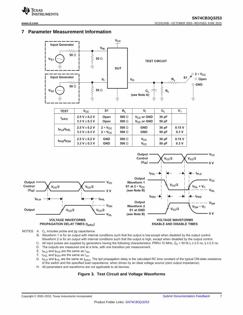
6.6 Switching Characteristicsover recommended operating free-air temperature range (unless otherwise noted) (see Figure 3)
VCC = 2.5 V VCC = 3.3 VFROM TO ± 0.2 V ± 0.3 VPARAMETER UNIT(INPUT) (OUTPUT)
MIN MAX MIN MAXf OE or fS(1) OE or S A or B 10 20 MHztpd
(2) A or B B or A 0.12 0.18 nstpd(s) S A 1.5 6.7 1.5 5.9 ns
S B 1.5 6.7 1.5 5.9ten ns
OE A or B 1.5 6.7 1.5 5.9S B 1 6.1 1 6.1
tdis nsOE A or B 1 6.1 1 6.1
(1) Maximum switching frequency for control input (VO > VCC, VI = 5 V, RL ≥ 1 MΩ, CL = 0).(2) The propagation delay is the calculated RC time constant of the typical ON-state resistance of the switch and the specified load
capacitance, when driven by an ideal voltage source (zero output impedance).
Copyright © 2003–2015, Texas Instruments Incorporated Submit Documentation Feedback 5
Product Folder Links: SN74CB3Q3253
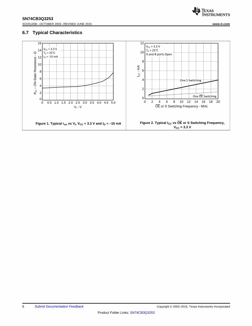
12
10
8
6
4
2
00 0.5 1.0 1.5 2.0 2.5 3.0 3.5 4.0 4.5 5.0
Ron
± O
N-S
tate
Res
ista
nce
-
VI - V
VCC = 3.3 V
TA = 25°C
IO = -15 mA
14
16 12
10
8
6
4
2
00 2 4 6 8 10 12 14 16 18 20
I CC -
mA
OE or S Switching Frequency - MHz
VCC = 3.3 V
TA = 25°C
A and B ports Open
One S Switching
One OE Switching
SN74CB3Q3253SCDS145B –OCTOBER 2003–REVISED JUNE 2015 www.ti.com
6.7 Typical Characteristics
Figure 2. Typical ICC vs OE or S Switching Frequency,Figure 1. Typical ron vs VI, VCC = 3.3 V and IO = –15 mAVCC = 3.3 V
6 Submit Documentation Feedback Copyright © 2003–2015, Texas Instruments Incorporated
Product Folder Links: SN74CB3Q3253
VOH
VOL
CL
(see Note A)
TEST CIRCUIT
S12 × VCC
Open
GND
RL
RL
tPLH tPHL
Output
Waveform 1
S1 at 2 × VCC
(see Note B)
Output
Waveform 2
S1 at GND
(see Note B)
tPZL
tPZH
tPLZ
tPHZ
VCC
0 V
VOH
VOL
0 V
VOL + VD
VOH − VD
0 V
Output
Control
(VIN)
VCC
VCC
VOLTAGE WAVEFORMS
PROPAGATION DELAY TIMES (tpd(s))
VOLTAGE WAVEFORMS
ENABLE AND DISABLE TIMES
Output
NOTES: A. CL includes probe and jig capacitance.
B. Waveform 1 is for an output with internal conditions such that the output is low, except when disabled by the output control.
Waveform 2 is for an output with internal conditions such that the output is high, except when disabled by the output control.
C. All input pulses are supplied by generators having the following characteristics: PRR≤ 10 MHz, ZO = 50 W, tr ≤ 2.5 ns, tf ≤ 2.5 ns.
D. The outputs are measured one at a time, with one transition per measurement.
E. tPLZ and tPHZ are the same as t dis.
F. tPZL and tPZH are the same as t en.
G. tPLH and tPHL are the same as tpd(s). The tpd propagation delay is the calculated RC time constant of the typical ON-state resistance
of the switch and the specified load capacitance, when driven by an ideal voltage source (zero output impedance).
H. All parameters and waveforms are not applicable to all devices.
50 Ω
VG1
VCC
DUT
50 Ω
VIN
50 Ω
VG2 50 Ω
VI
TEST RLS1 V∆CL
2.5 V ± 0.2 V
3.3 V ± 0.3 V
VCC VI
tPHZ/tPZH
tPLZ/tPZL
tpd(s)
2.5 V ± 0.2 V
3.3 V ± 0.3 V
2.5 V ± 0.2 V
3.3 V ± 0.3 V
Open
Open
2 × VCC
2 × VCC
GND
GND
500 Ω
500 Ω
500 Ω
500 Ω
500 Ω
500 Ω
VCC or GND
VCC or GND
GND
GND
VCC
VCC
30 pF
50 pF
30 pF
50 pF
30 pF
50 pF
0.15 V
0.3 V
0.15 V
0.3 V
Output
Control
(VIN)
Input Generator
Input Generator
VCC/2 VCC/2
VCC/2 VCC/2
VCC/2 VCC/2 VCC/2
VCC/2
VO
SN74CB3Q3253www.ti.com SCDS145B –OCTOBER 2003–REVISED JUNE 2015
7 Parameter Measurement Information
Figure 3. Test Circuit and Voltage Waveforms
Copyright © 2003–2015, Texas Instruments Incorporated Submit Documentation Feedback 7
Product Folder Links: SN74CB3Q3253
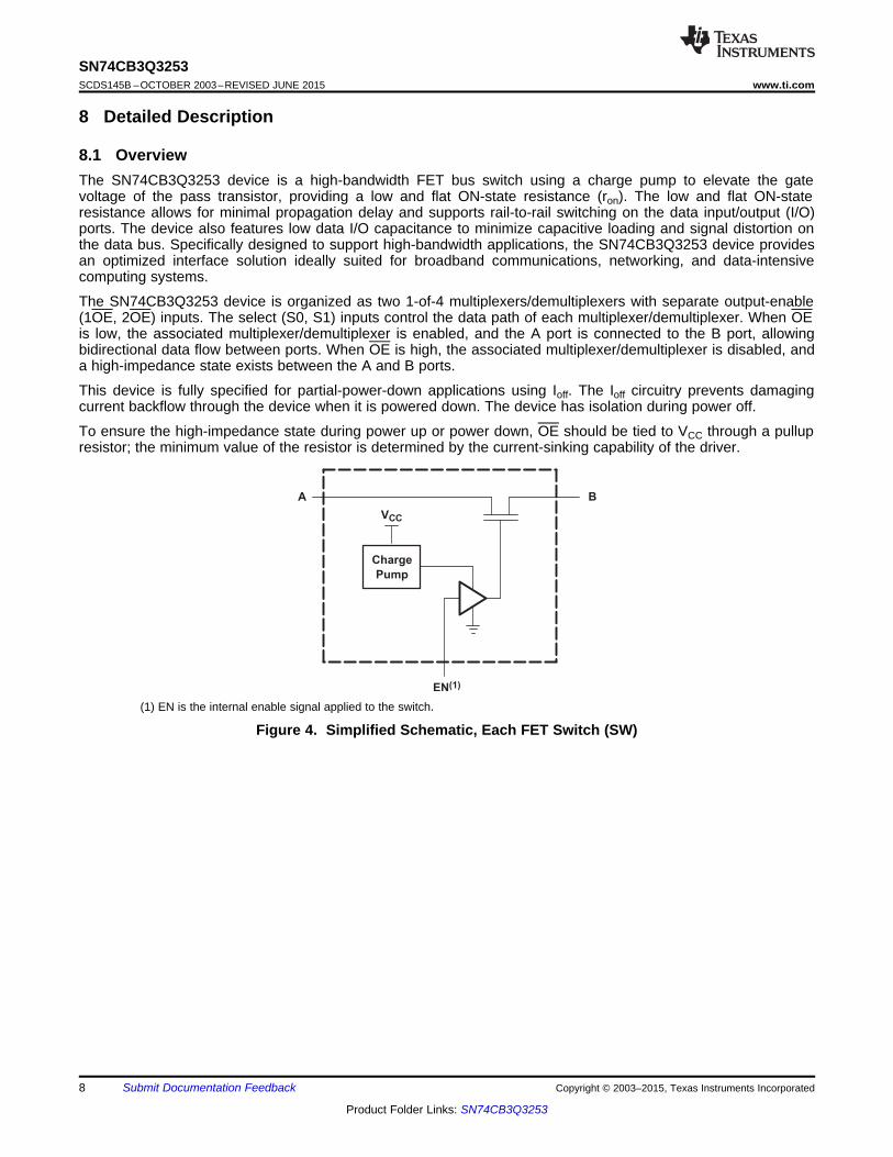
A
EN(1)
B
Charge
Pump
VCC
SN74CB3Q3253SCDS145B –OCTOBER 2003–REVISED JUNE 2015 www.ti.com
8 Detailed Description
8.1 OverviewThe SN74CB3Q3253 device is a high-bandwidth FET bus switch using a charge pump to elevate the gatevoltage of the pass transistor, providing a low and flat ON-state resistance (ron). The low and flat ON-stateresistance allows for minimal propagation delay and supports rail-to-rail switching on the data input/output (I/O)ports. The device also features low data I/O capacitance to minimize capacitive loading and signal distortion onthe data bus. Specifically designed to support high-bandwidth applications, the SN74CB3Q3253 device providesan optimized interface solution ideally suited for broadband communications, networking, and data-intensivecomputing systems.
The SN74CB3Q3253 device is organized as two 1-of-4 multiplexers/demultiplexers with separate output-enable(1OE, 2OE) inputs. The select (S0, S1) inputs control the data path of each multiplexer/demultiplexer. When OEis low, the associated multiplexer/demultiplexer is enabled, and the A port is connected to the B port, allowingbidirectional data flow between ports. When OE is high, the associated multiplexer/demultiplexer is disabled, anda high-impedance state exists between the A and B ports.
This device is fully specified for partial-power-down applications using Ioff. The Ioff circuitry prevents damagingcurrent backflow through the device when it is powered down. The device has isolation during power off.
To ensure the high-impedance state during power up or power down, OE should be tied to VCC through a pullupresistor; the minimum value of the resistor is determined by the current-sinking capability of the driver.
(1) EN is the internal enable signal applied to the switch.
Figure 4. Simplified Schematic, Each FET Switch (SW)
8 Submit Documentation Feedback Copyright © 2003–2015, Texas Instruments Incorporated
Product Folder Links: SN74CB3Q3253
2B1
1B1
2A
1A
S0
S1
1OE
2OE
1B2
1B3
1B4
2B2
2B3
2B4
SW
SW
SW
SW
SW
SW
SW
SW
7
9
14
2
1
15
6
5
4
3
10
11
12
13
SN74CB3Q3253www.ti.com SCDS145B –OCTOBER 2003–REVISED JUNE 2015
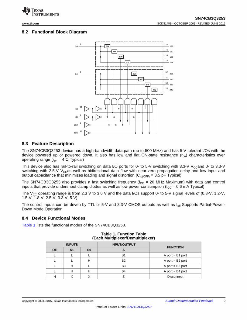
8.2 Functional Block Diagram
8.3 Feature DescriptionThe SN74CB3Q3253 device has a high-bandwidth data path (up to 500 MHz) and has 5-V tolerant I/Os with thedevice powered up or powered down. It also has low and flat ON-state resistance (ron) characteristics overoperating range (ron = 4 Ω Typical)
This device also has rail-to-rail switching on data I/O ports for 0- to 5-V switching with 3.3-V VCCand 0- to 3.3-Vswitching with 2.5-V VCCas well as bidirectional data flow with near-zero propagation delay and low input andoutput capacitance that minimizes loading and signal distortion (Cio(OFF) = 3.5 pF Typical)
The SN74CB3Q3253 also provides a fast switching frequency (fOE = 20 MHz Maximum) with data and controlinputs that provide undershoot clamp diodes as well as low power consumption (ICC = 0.6 mA Typical)
The VCC operating range is from 2.3 V to 3.6 V and the data I/Os support 0- to 5-V signal levels of (0.8-V, 1.2-V,1.5-V, 1.8-V, 2.5-V, 3.3-V, 5-V)
The control inputs can be driven by TTL or 5-V and 3.3-V CMOS outputs as well as Ioff Supports Partial-Power-Down Mode Operation
8.4 Device Functional ModesTable 1 lists the functional modes of the SN74CB3Q3253.
Table 1. Function Table(Each Multiplexer/Demultiplexer)
INPUTS INPUT/OUTPUTFUNCTION
OE S1 S0 AL L L B1 A port = B1 portL L H B2 A port = B2 portL H L B3 A port = B3 portL H H B4 A port = B4 portH X X Z Disconnect
Copyright © 2003–2015, Texas Instruments Incorporated Submit Documentation Feedback 9
Product Folder Links: SN74CB3Q3253
7
15
6
5
14
4
3
10
119
12
13
RON
SN74CB3Q3253
Bus Controller
2
2Device 1
Device 22
16
8GND
4A
1A
VCC
S01B1
1B2
1B3
1B4
2B1
2B2
2B3
2B41OE
0.1 PF
VCC
2S1 S1 S0
L L
L H
H L
H H
Switch
Select
Device 32
Device 42
RON
S1 S0L L
L H
H L
H H
1
2OE
SN74CB3Q3253SCDS145B –OCTOBER 2003–REVISED JUNE 2015 www.ti.com
9 Application and Implementation
NOTEInformation in the following applications sections is not part of the TI componentspecification, and TI does not warrant its accuracy or completeness. TI’s customers areresponsible for determining suitability of components for their purposes. Customers shouldvalidate and test their design implementation to confirm system functionality.
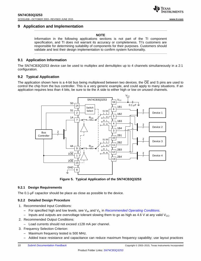
9.1 Application InformationThe SN74CB3Q3253 device can be used to multiplex and demultiplex up to 4 channels simultaneously in a 2:1configuration.
9.2 Typical ApplicationThe application shown here is a 4-bit bus being multiplexed between two devices. the OE and S pins are used tocontrol the chip from the bus controller. This is a very generic example, and could apply to many situations. If anapplication requires less than 4 bits, be sure to tie the A side to either high or low on unused channels.
Figure 5. Typical Application of the SN74CB3Q3253
9.2.1 Design RequirementsThe 0.1-µF capacitor should be place as close as possible to the device.
9.2.2 Detailed Design Procedure1. Recommended Input Conditions:
– For specified high and low levels, see VIH and VIL in Recommended Operating Conditions.– Inputs and outputs are overvoltage tolerant slowing them to go as high as 4.6 V at any valid VCC.
2. Recommended Output Conditions:– Load currents should not exceed ±128 mA per channel.
3. Frequency Selection Criterion:– Maximum frequency tested is 500 MHz.– Added trace resistance and capacitance can reduce maximum frequency capability; use layout practices
10 Submit Documentation Feedback Copyright © 2003–2015, Texas Instruments Incorporated
Product Folder Links: SN74CB3Q3253
0
1
2
3
0 100 200 300 400 500 600 700 800 900 1000
Vol
tage
(V
)
Time (ps)
VIN
VOUT
C001
SN74CB3Q3253www.ti.com SCDS145B –OCTOBER 2003–REVISED JUNE 2015
Typical Application (continued)as directed in Layout.
9.2.3 Application Curve
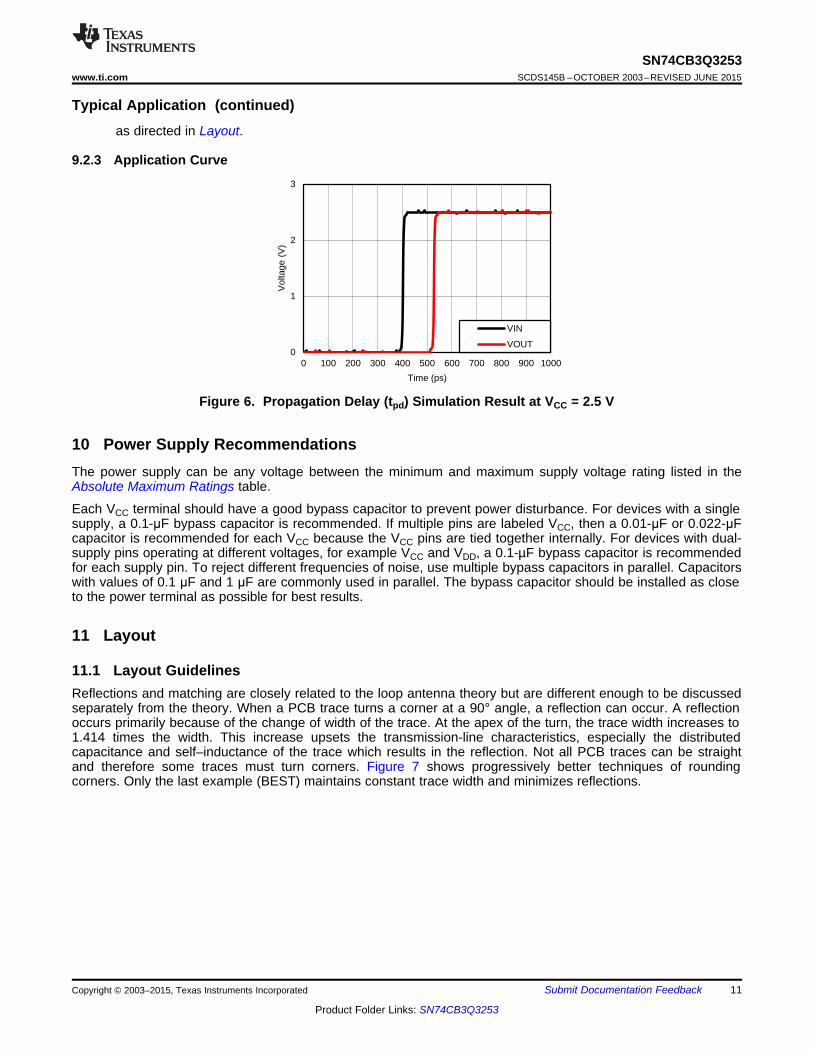
Figure 6. Propagation Delay (tpd) Simulation Result at VCC = 2.5 V
10 Power Supply RecommendationsThe power supply can be any voltage between the minimum and maximum supply voltage rating listed in theAbsolute Maximum Ratings table.
Each VCC terminal should have a good bypass capacitor to prevent power disturbance. For devices with a singlesupply, a 0.1-μF bypass capacitor is recommended. If multiple pins are labeled VCC, then a 0.01-μF or 0.022-μFcapacitor is recommended for each VCC because the VCC pins are tied together internally. For devices with dual-supply pins operating at different voltages, for example VCC and VDD, a 0.1-µF bypass capacitor is recommendedfor each supply pin. To reject different frequencies of noise, use multiple bypass capacitors in parallel. Capacitorswith values of 0.1 μF and 1 μF are commonly used in parallel. The bypass capacitor should be installed as closeto the power terminal as possible for best results.
11 Layout
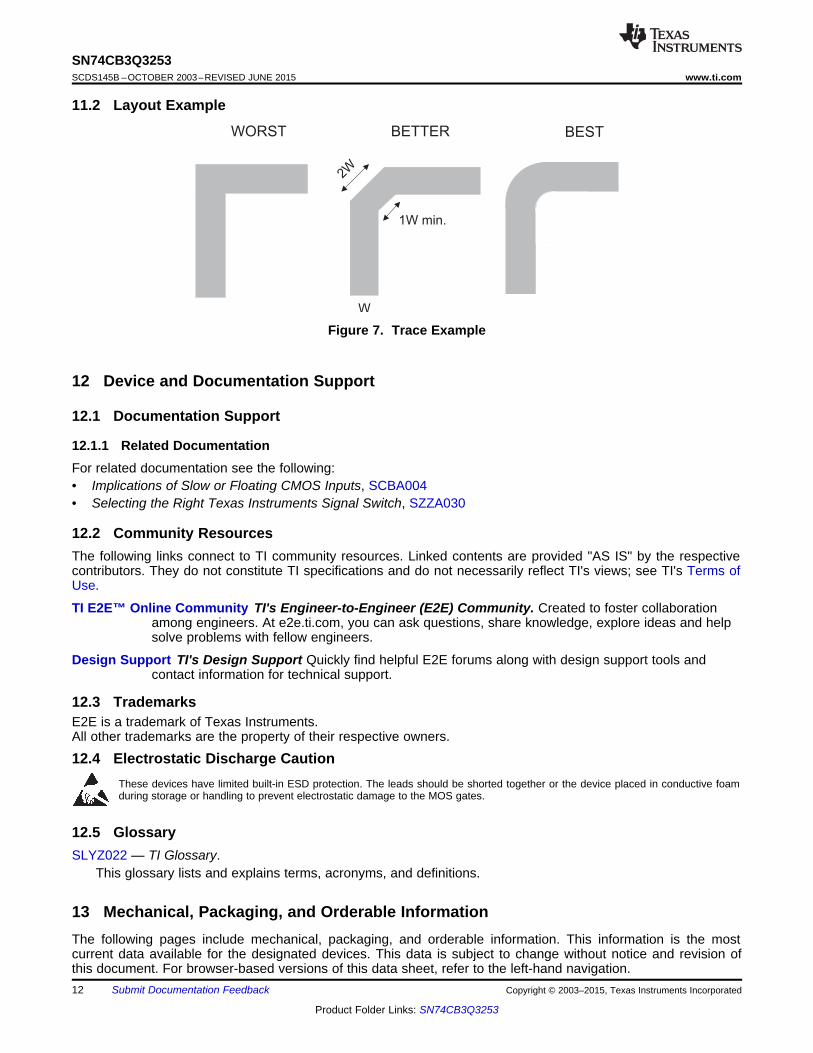
11.1 Layout GuidelinesReflections and matching are closely related to the loop antenna theory but are different enough to be discussedseparately from the theory. When a PCB trace turns a corner at a 90° angle, a reflection can occur. A reflectionoccurs primarily because of the change of width of the trace. At the apex of the turn, the trace width increases to1.414 times the width. This increase upsets the transmission-line characteristics, especially the distributedcapacitance and self–inductance of the trace which results in the reflection. Not all PCB traces can be straightand therefore some traces must turn corners. Figure 7 shows progressively better techniques of roundingcorners. Only the last example (BEST) maintains constant trace width and minimizes reflections.
Copyright © 2003–2015, Texas Instruments Incorporated Submit Documentation Feedback 11
Product Folder Links: SN74CB3Q3253
WORST BETTER BEST
1W min.
W
2W
SN74CB3Q3253SCDS145B –OCTOBER 2003–REVISED JUNE 2015 www.ti.com
11.2 Layout Example
Figure 7. Trace Example
12 Device and Documentation Support
12.1 Documentation Support
12.1.1 Related DocumentationFor related documentation see the following:• Implications of Slow or Floating CMOS Inputs, SCBA004• Selecting the Right Texas Instruments Signal Switch, SZZA030
12.2 Community ResourcesThe following links connect to TI community resources. Linked contents are provided "AS IS" by the respectivecontributors. They do not constitute TI specifications and do not necessarily reflect TI's views; see TI's Terms ofUse.
TI E2E™ Online Community TI's Engineer-to-Engineer (E2E) Community. Created to foster collaborationamong engineers. At e2e.ti.com, you can ask questions, share knowledge, explore ideas and helpsolve problems with fellow engineers.
Design Support TI's Design Support Quickly find helpful E2E forums along with design support tools andcontact information for technical support.
12.3 TrademarksE2E is a trademark of Texas Instruments.All other trademarks are the property of their respective owners.
12.4 Electrostatic Discharge CautionThese devices have limited built-in ESD protection. The leads should be shorted together or the device placed in conductive foamduring storage or handling to prevent electrostatic damage to the MOS gates.
12.5 GlossarySLYZ022 — TI Glossary.
This glossary lists and explains terms, acronyms, and definitions.
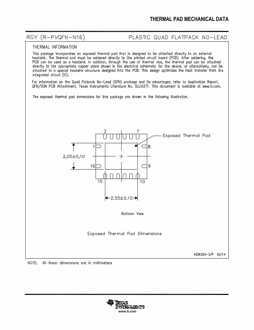
13 Mechanical, Packaging, and Orderable InformationThe following pages include mechanical, packaging, and orderable information. This information is the mostcurrent data available for the designated devices. This data is subject to change without notice and revision ofthis document. For browser-based versions of this data sheet, refer to the left-hand navigation.12 Submit Documentation Feedback Copyright © 2003–2015, Texas Instruments Incorporated
Product Folder Links: SN74CB3Q3253
PACKAGE OPTION ADDENDUM
www.ti.com 24-Apr-2015
Addendum-Page 1
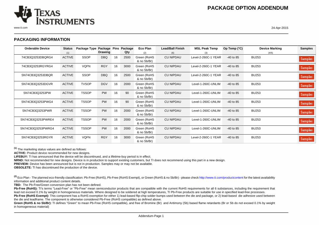
PACKAGING INFORMATION
Orderable Device Status(1)
Package Type PackageDrawing
Pins PackageQty
Eco Plan(2)
Lead/Ball Finish(6)
MSL Peak Temp(3)
Op Temp (°C) Device Marking(4/5)
Samples
74CB3Q3253DBQRG4 ACTIVE SSOP DBQ 16 2500 Green (RoHS& no Sb/Br)
CU NIPDAU Level-2-260C-1 YEAR -40 to 85 BU253
74CB3Q3253RGYRG4 ACTIVE VQFN RGY 16 3000 Green (RoHS& no Sb/Br)
CU NIPDAU Level-2-260C-1 YEAR -40 to 85 BU253
SN74CB3Q3253DBQR ACTIVE SSOP DBQ 16 2500 Green (RoHS& no Sb/Br)
CU NIPDAU Level-2-260C-1 YEAR -40 to 85 BU253
SN74CB3Q3253DGVR ACTIVE TVSOP DGV 16 2000 Green (RoHS& no Sb/Br)
CU NIPDAU Level-1-260C-UNLIM -40 to 85 BU253
SN74CB3Q3253PW ACTIVE TSSOP PW 16 90 Green (RoHS& no Sb/Br)
CU NIPDAU Level-1-260C-UNLIM -40 to 85 BU253
SN74CB3Q3253PWG4 ACTIVE TSSOP PW 16 90 Green (RoHS& no Sb/Br)
CU NIPDAU Level-1-260C-UNLIM -40 to 85 BU253
SN74CB3Q3253PWR ACTIVE TSSOP PW 16 2000 Green (RoHS& no Sb/Br)
CU NIPDAU Level-1-260C-UNLIM -40 to 85 BU253
SN74CB3Q3253PWRE4 ACTIVE TSSOP PW 16 2000 Green (RoHS& no Sb/Br)
CU NIPDAU Level-1-260C-UNLIM -40 to 85 BU253
SN74CB3Q3253PWRG4 ACTIVE TSSOP PW 16 2000 Green (RoHS& no Sb/Br)
CU NIPDAU Level-1-260C-UNLIM -40 to 85 BU253
SN74CB3Q3253RGYR ACTIVE VQFN RGY 16 3000 Green (RoHS& no Sb/Br)
CU NIPDAU Level-2-260C-1 YEAR -40 to 85 BU253
(1) The marketing status values are defined as follows:ACTIVE: Product device recommended for new designs.LIFEBUY: TI has announced that the device will be discontinued, and a lifetime-buy period is in effect.NRND: Not recommended for new designs. Device is in production to support existing customers, but TI does not recommend using this part in a new design.PREVIEW: Device has been announced but is not in production. Samples may or may not be available.OBSOLETE: TI has discontinued the production of the device.
(2) Eco Plan - The planned eco-friendly classification: Pb-Free (RoHS), Pb-Free (RoHS Exempt), or Green (RoHS & no Sb/Br) - please check http://www.ti.com/productcontent for the latest availabilityinformation and additional product content details.TBD: The Pb-Free/Green conversion plan has not been defined.Pb-Free (RoHS): TI's terms "Lead-Free" or "Pb-Free" mean semiconductor products that are compatible with the current RoHS requirements for all 6 substances, including the requirement thatlead not exceed 0.1% by weight in homogeneous materials. Where designed to be soldered at high temperatures, TI Pb-Free products are suitable for use in specified lead-free processes.Pb-Free (RoHS Exempt): This component has a RoHS exemption for either 1) lead-based flip-chip solder bumps used between the die and package, or 2) lead-based die adhesive used betweenthe die and leadframe. The component is otherwise considered Pb-Free (RoHS compatible) as defined above.Green (RoHS & no Sb/Br): TI defines "Green" to mean Pb-Free (RoHS compatible), and free of Bromine (Br) and Antimony (Sb) based flame retardants (Br or Sb do not exceed 0.1% by weightin homogeneous material)
PACKAGE OPTION ADDENDUM
www.ti.com 24-Apr-2015
Addendum-Page 2
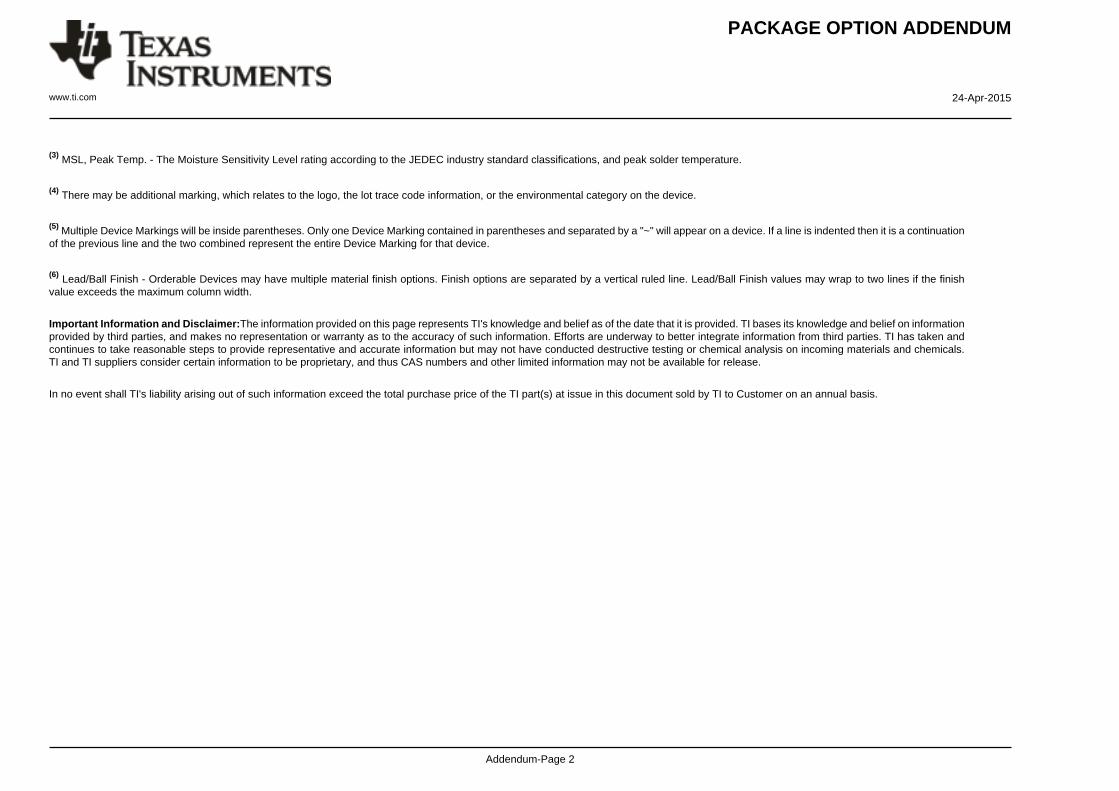
(3) MSL, Peak Temp. - The Moisture Sensitivity Level rating according to the JEDEC industry standard classifications, and peak solder temperature.
(4) There may be additional marking, which relates to the logo, the lot trace code information, or the environmental category on the device.
(5) Multiple Device Markings will be inside parentheses. Only one Device Marking contained in parentheses and separated by a "~" will appear on a device. If a line is indented then it is a continuationof the previous line and the two combined represent the entire Device Marking for that device.
(6) Lead/Ball Finish - Orderable Devices may have multiple material finish options. Finish options are separated by a vertical ruled line. Lead/Ball Finish values may wrap to two lines if the finishvalue exceeds the maximum column width.
Important Information and Disclaimer:The information provided on this page represents TI's knowledge and belief as of the date that it is provided. TI bases its knowledge and belief on informationprovided by third parties, and makes no representation or warranty as to the accuracy of such information. Efforts are underway to better integrate information from third parties. TI has taken andcontinues to take reasonable steps to provide representative and accurate information but may not have conducted destructive testing or chemical analysis on incoming materials and chemicals.TI and TI suppliers consider certain information to be proprietary, and thus CAS numbers and other limited information may not be available for release.
In no event shall TI's liability arising out of such information exceed the total purchase price of the TI part(s) at issue in this document sold by TI to Customer on an annual basis.
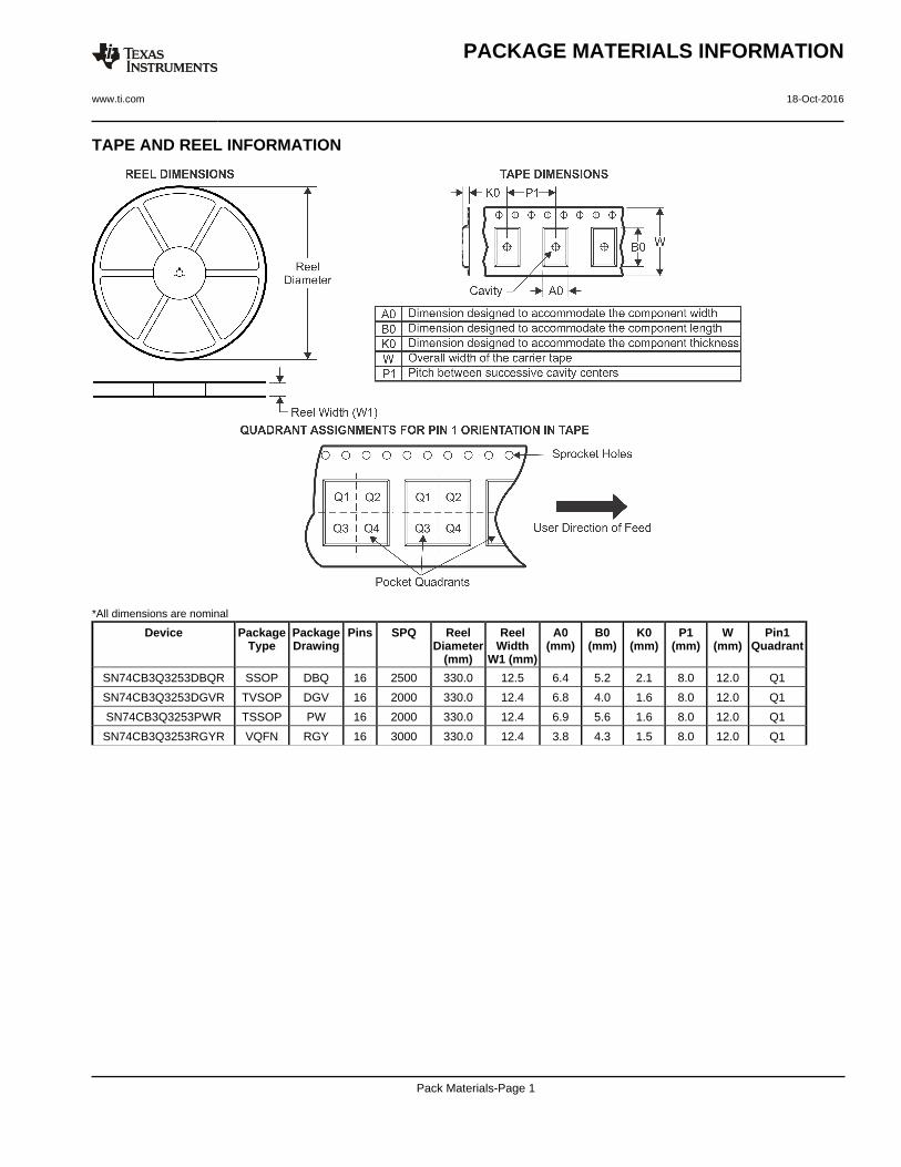
TAPE AND REEL INFORMATION
*All dimensions are nominal
Device PackageType
PackageDrawing
Pins SPQ ReelDiameter
(mm)
ReelWidth
W1 (mm)
A0(mm)
B0(mm)
K0(mm)
P1(mm)
W(mm)
Pin1Quadrant
SN74CB3Q3253DBQR SSOP DBQ 16 2500 330.0 12.5 6.4 5.2 2.1 8.0 12.0 Q1
SN74CB3Q3253DGVR TVSOP DGV 16 2000 330.0 12.4 6.8 4.0 1.6 8.0 12.0 Q1
SN74CB3Q3253PWR TSSOP PW 16 2000 330.0 12.4 6.9 5.6 1.6 8.0 12.0 Q1
SN74CB3Q3253RGYR VQFN RGY 16 3000 330.0 12.4 3.8 4.3 1.5 8.0 12.0 Q1
PACKAGE MATERIALS INFORMATION
www.ti.com 18-Oct-2016
Pack Materials-Page 1
*All dimensions are nominal
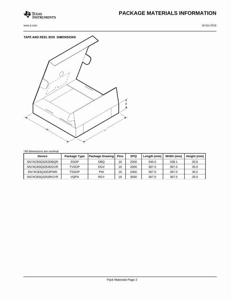
Device Package Type Package Drawing Pins SPQ Length (mm) Width (mm) Height (mm)
SN74CB3Q3253DBQR SSOP DBQ 16 2500 340.5 338.1 20.6
SN74CB3Q3253DGVR TVSOP DGV 16 2000 367.0 367.0 35.0
SN74CB3Q3253PWR TSSOP PW 16 2000 367.0 367.0 35.0
SN74CB3Q3253RGYR VQFN RGY 16 3000 367.0 367.0 35.0
PACKAGE MATERIALS INFORMATION
www.ti.com 18-Oct-2016
Pack Materials-Page 2
MECHANICAL DATA
MPDS006C – FEBRUARY 1996 – REVISED AUGUST 2000
POST OFFICE BOX 655303 • DALLAS, TEXAS 75265
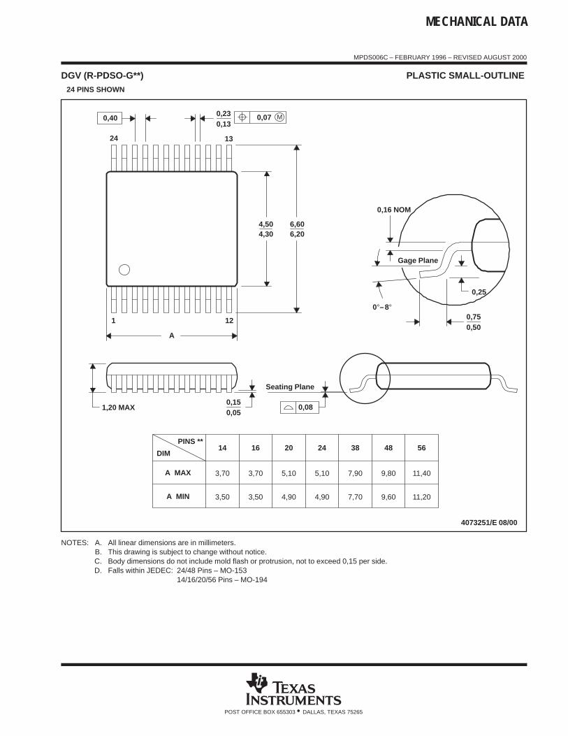
DGV (R-PDSO-G**) PLASTIC SMALL-OUTLINE 24 PINS SHOWN
14
3,70
3,50 4,90
5,10
20DIM
PINS **
4073251/E 08/00
1,20 MAX
Seating Plane
0,050,15
0,25
0,500,75
0,230,13
1 12
24 13
4,304,50
0,16 NOM
Gage Plane
A
7,90
7,70
382416
4,90
5,103,70
3,50
A MAX
A MIN
6,606,20
11,20
11,40
56
9,60
9,80
48
0,08
M0,070,40
0°–8°
NOTES: A. All linear dimensions are in millimeters.B. This drawing is subject to change without notice.C. Body dimensions do not include mold flash or protrusion, not to exceed 0,15 per side.D. Falls within JEDEC: 24/48 Pins – MO-153
14/16/20/56 Pins – MO-194
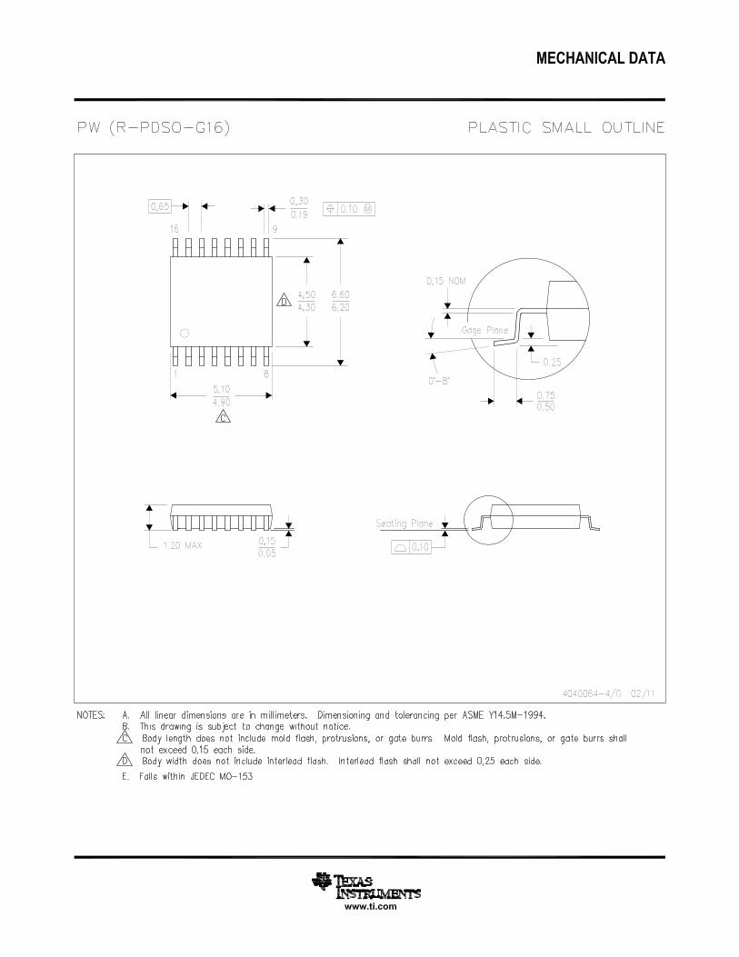
www.ti.com
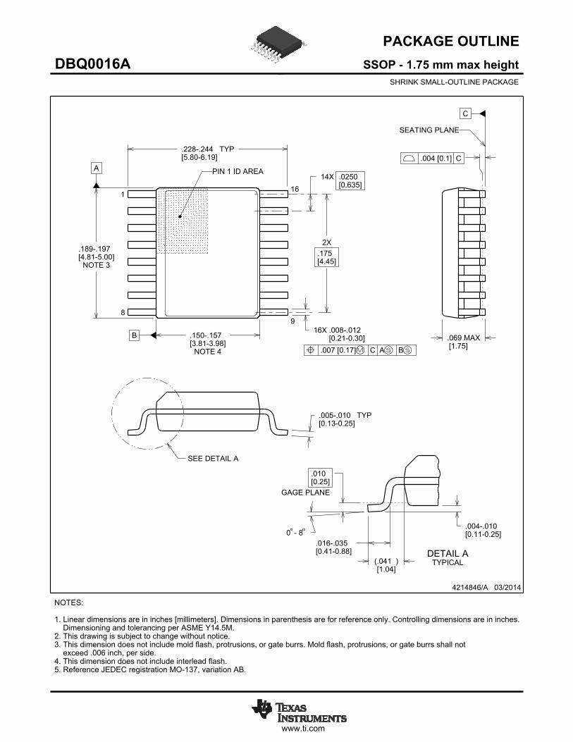
PACKAGE OUTLINE
C
TYP-.244.228-6.195.80[ ]
.069 MAX[1.75]
14X .0250[0.635]
16X -.012.008-0.300.21[ ]
2X.175[4.45]
TYP-.010.005-0.250.13[ ]
0 - 8-.010.004-0.250.11[ ]
(.041 )[1.04]
.010[0.25]
GAGE PLANE
-.035.016-0.880.41[ ]
A
NOTE 3
-.197.189-5.004.81[ ]
B
NOTE 4
-.157.150-3.983.81[ ]
SSOP - 1.75 mm max heightDBQ0016ASHRINK SMALL-OUTLINE PACKAGE
4214846/A 03/2014
NOTES: 1. Linear dimensions are in inches [millimeters]. Dimensions in parenthesis are for reference only. Controlling dimensions are in inches. Dimensioning and tolerancing per ASME Y14.5M. 2. This drawing is subject to change without notice. 3. This dimension does not include mold flash, protrusions, or gate burrs. Mold flash, protrusions, or gate burrs shall not exceed .006 inch, per side. 4. This dimension does not include interlead flash.5. Reference JEDEC registration MO-137, variation AB.
116
.007 [0.17] C A B
98
PIN 1 ID AREA
SEATING PLANE
.004 [0.1] C
SEE DETAIL A
DETAIL ATYPICAL
SCALE 2.800
www.ti.com
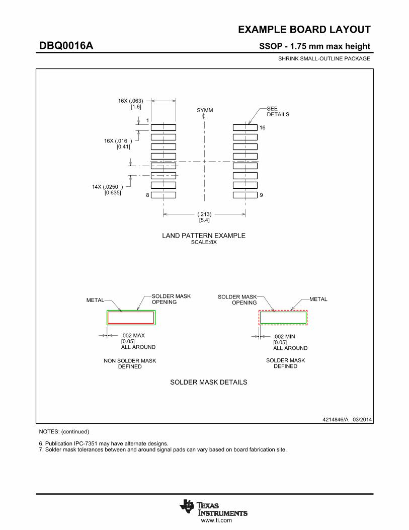
EXAMPLE BOARD LAYOUT
.002 MAX[0.05]ALL AROUND
.002 MIN[0.05]ALL AROUND
(.213)[5.4]
14X (.0250 )[0.635]
16X (.063)[1.6]
16X (.016 )[0.41]
SSOP - 1.75 mm max heightDBQ0016ASHRINK SMALL-OUTLINE PACKAGE
4214846/A 03/2014
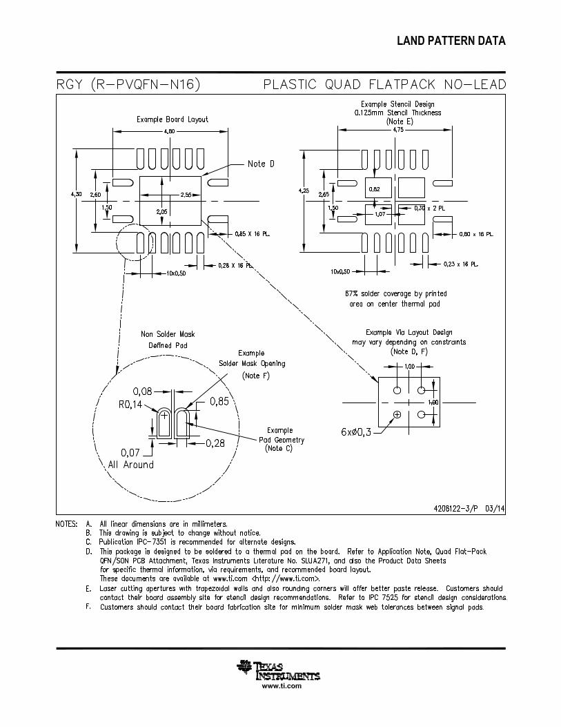
NOTES: (continued) 6. Publication IPC-7351 may have alternate designs. 7. Solder mask tolerances between and around signal pads can vary based on board fabrication site.
METALSOLDER MASKOPENING
NON SOLDER MASKDEFINED
SOLDER MASK DETAILS
OPENINGSOLDER MASK METAL
SOLDER MASKDEFINED
LAND PATTERN EXAMPLESCALE:8X
SYMM
1
8 9
16
SEEDETAILS
www.ti.com
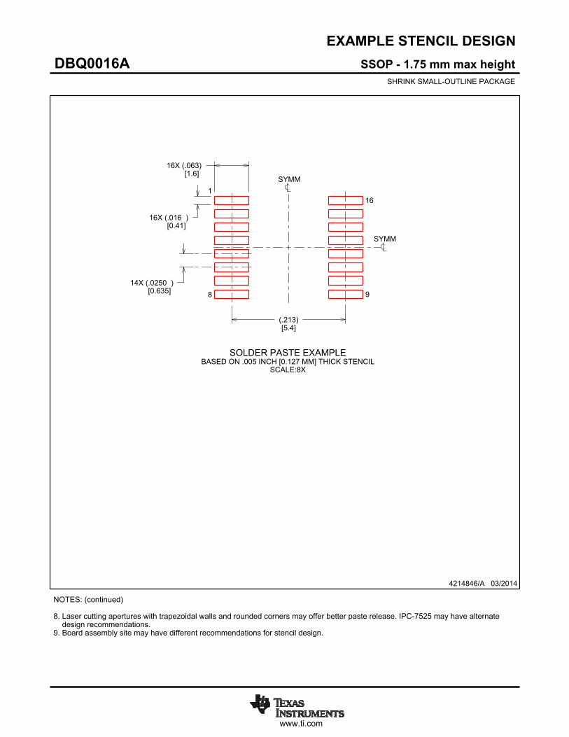
EXAMPLE STENCIL DESIGN
16X (.063)[1.6]
16X (.016 )[0.41]
14X (.0250 )[0.635]
(.213)[5.4]
SSOP - 1.75 mm max heightDBQ0016ASHRINK SMALL-OUTLINE PACKAGE
4214846/A 03/2014
NOTES: (continued) 8. Laser cutting apertures with trapezoidal walls and rounded corners may offer better paste release. IPC-7525 may have alternate design recommendations. 9. Board assembly site may have different recommendations for stencil design.
SOLDER PASTE EXAMPLEBASED ON .005 INCH [0.127 MM] THICK STENCIL
SCALE:8X
SYMM
SYMM
1
8 9
16
IMPORTANT NOTICE
Texas Instruments Incorporated (TI) reserves the right to make corrections, enhancements, improvements and other changes to itssemiconductor products and services per JESD46, latest issue, and to discontinue any product or service per JESD48, latest issue. Buyersshould obtain the latest relevant information before placing orders and should verify that such information is current and complete.TI’s published terms of sale for semiconductor products (http://www.ti.com/sc/docs/stdterms.htm) apply to the sale of packaged integratedcircuit products that TI has qualified and released to market. Additional terms may apply to the use or sale of other types of TI products andservices.Reproduction of significant portions of TI information in TI data sheets is permissible only if reproduction is without alteration and isaccompanied by all associated warranties, conditions, limitations, and notices. TI is not responsible or liable for such reproduceddocumentation. Information of third parties may be subject to additional restrictions. Resale of TI products or services with statementsdifferent from or beyond the parameters stated by TI for that product or service voids all express and any implied warranties for theassociated TI product or service and is an unfair and deceptive business practice. TI is not responsible or liable for any such statements.Buyers and others who are developing systems that incorporate TI products (collectively, “Designers”) understand and agree that Designersremain responsible for using their independent analysis, evaluation and judgment in designing their applications and that Designers havefull and exclusive responsibility to assure the safety of Designers' applications and compliance of their applications (and of all TI productsused in or for Designers’ applications) with all applicable regulations, laws and other applicable requirements. Designer represents that, withrespect to their applications, Designer has all the necessary expertise to create and implement safeguards that (1) anticipate dangerousconsequences of failures, (2) monitor failures and their consequences, and (3) lessen the likelihood of failures that might cause harm andtake appropriate actions. Designer agrees that prior to using or distributing any applications that include TI products, Designer willthoroughly test such applications and the functionality of such TI products as used in such applications.TI’s provision of technical, application or other design advice, quality characterization, reliability data or other services or information,including, but not limited to, reference designs and materials relating to evaluation modules, (collectively, “TI Resources”) are intended toassist designers who are developing applications that incorporate TI products; by downloading, accessing or using TI Resources in anyway, Designer (individually or, if Designer is acting on behalf of a company, Designer’s company) agrees to use any particular TI Resourcesolely for this purpose and subject to the terms of this Notice.TI’s provision of TI Resources does not expand or otherwise alter TI’s applicable published warranties or warranty disclaimers for TIproducts, and no additional obligations or liabilities arise from TI providing such TI Resources. TI reserves the right to make corrections,enhancements, improvements and other changes to its TI Resources. TI has not conducted any testing other than that specificallydescribed in the published documentation for a particular TI Resource.Designer is authorized to use, copy and modify any individual TI Resource only in connection with the development of applications thatinclude the TI product(s) identified in such TI Resource. NO OTHER LICENSE, EXPRESS OR IMPLIED, BY ESTOPPEL OR OTHERWISETO ANY OTHER TI INTELLECTUAL PROPERTY RIGHT, AND NO LICENSE TO ANY TECHNOLOGY OR INTELLECTUAL PROPERTYRIGHT OF TI OR ANY THIRD PARTY IS GRANTED HEREIN, including but not limited to any patent right, copyright, mask work right, orother intellectual property right relating to any combination, machine, or process in which TI products or services are used. Informationregarding or referencing third-party products or services does not constitute a license to use such products or services, or a warranty orendorsement thereof. Use of TI Resources may require a license from a third party under the patents or other intellectual property of thethird party, or a license from TI under the patents or other intellectual property of TI.TI RESOURCES ARE PROVIDED “AS IS” AND WITH ALL FAULTS. TI DISCLAIMS ALL OTHER WARRANTIES ORREPRESENTATIONS, EXPRESS OR IMPLIED, REGARDING RESOURCES OR USE THEREOF, INCLUDING BUT NOT LIMITED TOACCURACY OR COMPLETENESS, TITLE, ANY EPIDEMIC FAILURE WARRANTY AND ANY IMPLIED WARRANTIES OFMERCHANTABILITY, FITNESS FOR A PARTICULAR PURPOSE, AND NON-INFRINGEMENT OF ANY THIRD PARTY INTELLECTUALPROPERTY RIGHTS. TI SHALL NOT BE LIABLE FOR AND SHALL NOT DEFEND OR INDEMNIFY DESIGNER AGAINST ANY CLAIM,INCLUDING BUT NOT LIMITED TO ANY INFRINGEMENT CLAIM THAT RELATES TO OR IS BASED ON ANY COMBINATION OFPRODUCTS EVEN IF DESCRIBED IN TI RESOURCES OR OTHERWISE. IN NO EVENT SHALL TI BE LIABLE FOR ANY ACTUAL,DIRECT, SPECIAL, COLLATERAL, INDIRECT, PUNITIVE, INCIDENTAL, CONSEQUENTIAL OR EXEMPLARY DAMAGES INCONNECTION WITH OR ARISING OUT OF TI RESOURCES OR USE THEREOF, AND REGARDLESS OF WHETHER TI HAS BEENADVISED OF THE POSSIBILITY OF SUCH DAMAGES.Unless TI has explicitly designated an individual product as meeting the requirements of a particular industry standard (e.g., ISO/TS 16949and ISO 26262), TI is not responsible for any failure to meet such industry standard requirements.Where TI specifically promotes products as facilitating functional safety or as compliant with industry functional safety standards, suchproducts are intended to help enable customers to design and create their own applications that meet applicable functional safety standardsand requirements. Using products in an application does not by itself establish any safety features in the application. Designers mustensure compliance with safety-related requirements and standards applicable to their applications. Designer may not use any TI products inlife-critical medical equipment unless authorized officers of the parties have executed a special contract specifically governing such use.Life-critical medical equipment is medical equipment where failure of such equipment would cause serious bodily injury or death (e.g., lifesupport, pacemakers, defibrillators, heart pumps, neurostimulators, and implantables). Such equipment includes, without limitation, allmedical devices identified by the U.S. Food and Drug Administration as Class III devices and equivalent classifications outside the U.S.TI may expressly designate certain products as completing a particular qualification (e.g., Q100, Military Grade, or Enhanced Product).Designers agree that it has the necessary expertise to select the product with the appropriate qualification designation for their applicationsand that proper product selection is at Designers’ own risk. Designers are solely responsible for compliance with all legal and regulatoryrequirements in connection with such selection.Designer will fully indemnify TI and its representatives against any damages, costs, losses, and/or liabilities arising out of Designer’s non-compliance with the terms and provisions of this Notice.
Mailing Address: Texas Instruments, Post Office Box 655303, Dallas, Texas 75265Copyright © 2017, Texas Instruments Incorporated