Embed Size (px)
Citation preview
8/6/2019 Section 19. Voltage Reference
http://slidepdf.com/reader/full/section-19-voltage-reference 1/10
© 1997 Microchip Technology Inc. DS31019A page 19-1
MSection 19. Voltage Reference
HIGHLIGHTS
This section of the manual contains the following major topics:
19.1 Introduction ..................................................................................................................19-2
19.2 Control Register ...........................................................................................................19-3
19.3 Configuring the Voltage Reference ..............................................................................19-4
19.4 Voltage Reference Accuracy/Error ...............................................................................19-5
19.5 Operation During Sleep ...............................................................................................19-5
19.6 Effects of a Reset.........................................................................................................19-5
19.7 Connection Considerations..........................................................................................19-6
19.8 Initialization ..................................................................................................................19-7
19.9 Design Tips ..................................................................................................................19-8
19.10 Related Application Notes............................................................................................19-9
19.11 Revision History .........................................................................................................19-10
8/6/2019 Section 19. Voltage Reference
http://slidepdf.com/reader/full/section-19-voltage-reference 2/10
PICmicro MID-RANGE MCU FAMILY
DS31019A-page 19-2 © 1997 Microchip Technology Inc.
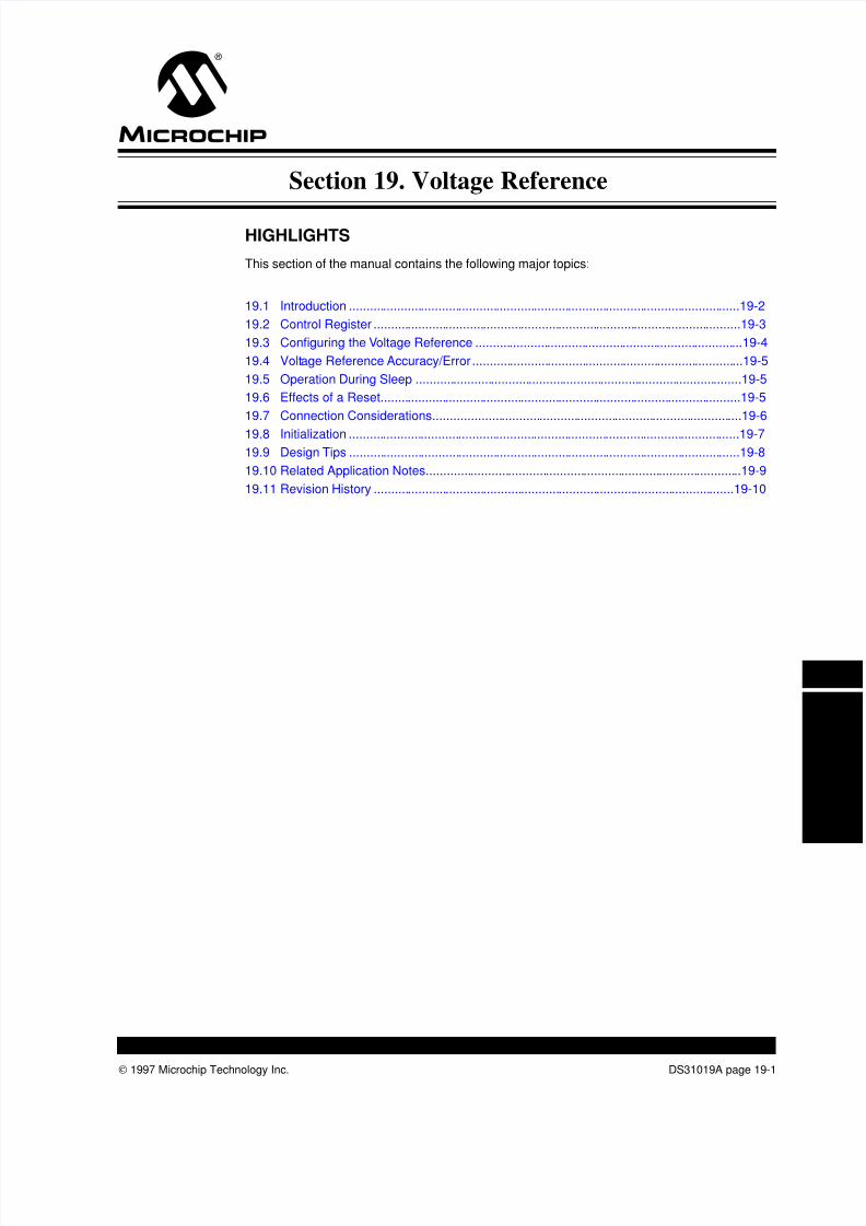
19.1 Introduction
The Voltage Reference module is typically used in conjunction with the Comparator module. The
comparator module’s inputs do not require very large drive, and therefore the drive capability of
the Voltage Reference is limited.
The Voltage Reference is a 16-tap resistor ladder network that provides a selectable voltage ref-
erence. The resistor ladder is segmented to provide two ranges of V REF values and has a
power-down function to conserve power when the reference is not being used. The VRCON reg-
ister controls the operation of the reference as shown in Figure 19-1. The block diagram is givenin Figure 19-1. Within each range, the 16 steps are monotonic (i.e. each increasing code will
result in an increasing output).
Figure 19-1: Voltage Reference Block Diagram
Table 19-1: Typical Voltage Reference with VDD = 5.0V
VR3:VR0VREF
VRR = 1 VRR = 0
0000 0.00 V 1.25 V0001 0.21 V 1.41 V
0010 0.42 V 1.56 V
0011 0.63 V 1.72 V
0100 0.83 V 1.88 V
0101 1.04 V 2.03 V
0110 1.25 V 2.19 V
0111 1.46 V 2.34 V
1000 1.67 V 2.50 V
1001 1.88 V 2.66 V
1010 2.08 V 2.81 V
1011 2.29 V 2.97 V
1100 2.50 V 3.13 V
1101 2.71 V 3.28 V
1110 2.92 V 3.44 V
1111 3.13 V 3.59 V
Note 1: See parameter D312 in the Electrical Specifications section of the device data sheet.
VRR8R(1)
VR3
VR0(From VRCON<3:0>)16-1 Analog MUX
8R(1) R(1) R(1) R(1) R(1)VREN
VREF
16 Stages
8/6/2019 Section 19. Voltage Reference
http://slidepdf.com/reader/full/section-19-voltage-reference 3/10
© 1997 Microchip Technology Inc. DS31019A-page 19-3
Section 19. Voltage Reference
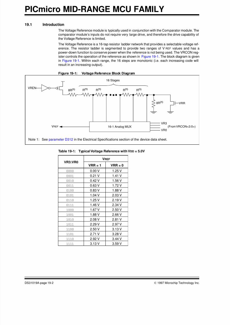
19.2 Control Register
Register 19-1: VRCON Register
R/W-0 R/W-0 R/W-0 U-0 R/W-0 R/W-0 R/W-0 R/W-0
VREN VROE VRR — VR3 VR2 VR1 VR0
bit 7 bit 0
bit 7 VREN: VREF Enable
1 = VREF circuit powered on
0 = VREF circuit powered down
bit 6 VROE: VREF Output Enable
1 = VREF is internally connected to Comparator module’s VREF. This voltage level is also
output on the VREF pin
0 = VREF is not connected to the comparator module. This voltage is disconnected from the
VREF pin
bit 5 VRR: VREF Range selection
1 = 0V to 0.75 VDD, with VDD /24 step size
0 = 0.25 VDD to 0.75 VDD, with VDD /32 step size
bit 4 Unimplemented: Read as '0'
bit 3:0 VR3:VR0: VREF value selection 0 ≤ VR3:VR0 ≤ 15
When VRR = 1:
VREF = (VR<3:0>/ 24) • VDD
When VRR = 0:
VREF = 1/4 * VDD + (VR3:VR0/ 32) • VDD
Legend
R = Readable bit W = Writable bit
U = Unimplemented bit, read as ‘0’ - n = Value at POR reset
8/6/2019 Section 19. Voltage Reference
http://slidepdf.com/reader/full/section-19-voltage-reference 4/10
PICmicro MID-RANGE MCU FAMILY
DS31019A-page 19-4 © 1997 Microchip Technology Inc.
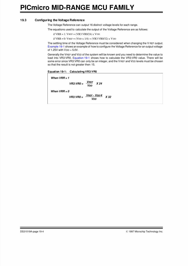
19.3 Configuring the Voltage Reference
The Voltage Reference can output 16 distinct voltage levels for each range.
The equations used to calculate the output of the Voltage Reference are as follows:
if VRR = 1: VREF = (VR3:VR0/24) x VDD
if VRR = 0: VREF = (VDD x 1/4) + (VR3:VR0/32) x VDD
The settling time of the Voltage Reference must be considered when changing the VREF output.
Example 19-1 shows an example of how to configure the Voltage Reference for an output voltageof 1.25V with VDD = 5.0V.
Generally the VREF and VDD of the system will be known and you need to determine the value to
load into VR3:VR0. Equation 19-1 shows how to calculate the VR3:VR0 value. There will be
some error since VR3:VR0 can only be an integer, and the VREF and VDD levels must be chosen
so that the result is not greater then 15.
Equation 19-1: Calculating VR3:VR0
V REF
V DD X 24 VR3:VR0 =
When VRR = 1
V REF - V DD /4
V DD X 32 VR3:VR0 =
When VRR = 0
8/6/2019 Section 19. Voltage Reference
http://slidepdf.com/reader/full/section-19-voltage-reference 5/10
8/6/2019 Section 19. Voltage Reference
http://slidepdf.com/reader/full/section-19-voltage-reference 6/10
PICmicro MID-RANGE MCU FAMILY
DS31019A-page 19-6 © 1997 Microchip Technology Inc.
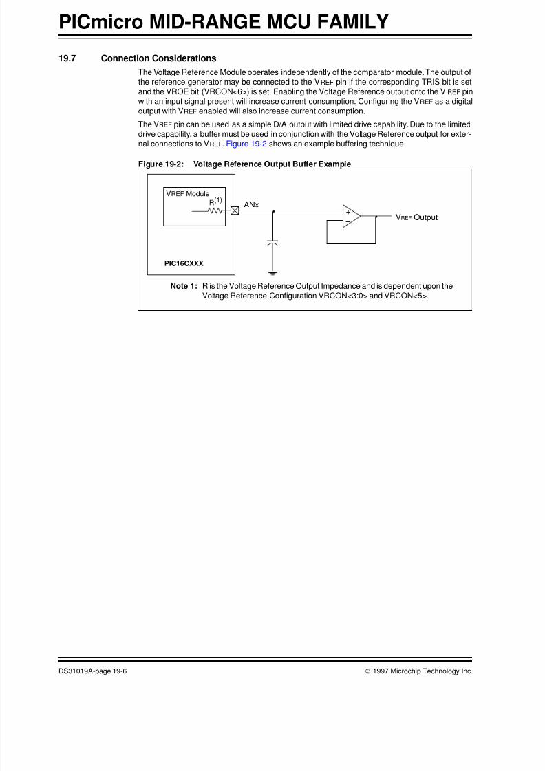
19.7 Connection Considerations
The Voltage Reference Module operates independently of the comparator module. The output of
the reference generator may be connected to the VREF pin if the corresponding TRIS bit is set
and the VROE bit (VRCON<6>) is set. Enabling the Voltage Reference output onto the VREF pin
with an input signal present will increase current consumption. Configuring the VREF as a digital
output with VREF enabled will also increase current consumption.
The VREF pin can be used as a simple D/A output with limited drive capability. Due to the limited
drive capability, a buffer must be used in conjunction with the Voltage Reference output for exter-nal connections to VREF. Figure 19-2 shows an example buffering technique.
Figure 19-2: Voltage Reference Output Buffer Example
VREF Output+
– •
•
VREF Module
R(1)ANx
Note 1: R is the Voltage Reference Output Impedance and is dependent upon the
Voltage Reference Configuration VRCON<3:0> and VRCON<5>.
PIC16CXXX
8/6/2019 Section 19. Voltage Reference
http://slidepdf.com/reader/full/section-19-voltage-reference 7/10
© 1997 Microchip Technology Inc. DS31019A-page 19-7
Section 19. Voltage Reference
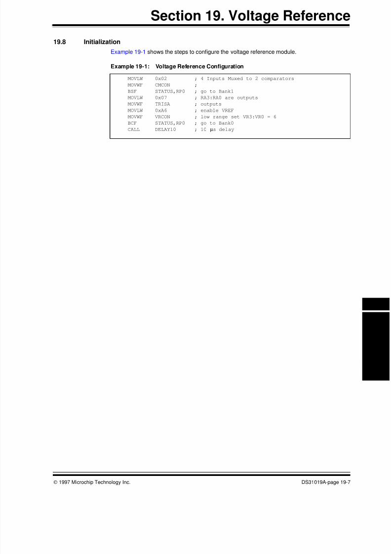
19.8 Initialization
Example 19-1 shows the steps to configure the voltage reference module.
Example 19-1: Voltage Reference Configuration
MOVLW 0x02 ; 4 Inputs Muxed to 2 comparators
MOVWF CMCON ;
BSF STATUS,RP0 ; go to Bank1
MOVLW 0x07 ; RA3:RA0 are outputs
MOVWF TRISA ; outputs
MOVLW 0xA6 ; enable VREF
MOVWF VRCON ; low range set VR3:VR0 = 6
BCF STATUS,RP0 ; go to Bank0
CALL DELAY10 ; 10 µs delay
8/6/2019 Section 19. Voltage Reference
http://slidepdf.com/reader/full/section-19-voltage-reference 8/10
PICmicro MID-RANGE MCU FAMILY
DS31019A-page 19-8 © 1997 Microchip Technology Inc.
19.9 Design Tips
Question 1: My V REF is not what I expect.
Answer 1:
Any variation of the device VDD will translate directly onto the VREF pin. Also ensure that you have
correctly calculated (specified) the VDD divider which generates the VREF.
Question 2: I am connecting V REF into a low impedance circuit, and the V REF is not at the expected level.
Answer 2:
The Voltage Reference module is not intended to drive large loads. A buffer must be used
between the PICmicro’s VREF pin and the load.
8/6/2019 Section 19. Voltage Reference
http://slidepdf.com/reader/full/section-19-voltage-reference 9/10
© 1997 Microchip Technology Inc. DS31019A-page 19-9
Section 19. Voltage Reference
19.10 Related Application Notes
This section lists application notes that are related to this section of the manual. These applica-
tion notes may not be written specifically for the Mid-Range MCU family (that is they may be writ-
ten for the Base-Line, or High-End families), but the concepts are pertinent, and could be used
(with modification and possible limitations). The current application notes related to Voltage Ref-
erence are:
Title Application Note #
Resistance and Capacitance Meter using a PIC16C622 AN611
8/6/2019 Section 19. Voltage Reference
http://slidepdf.com/reader/full/section-19-voltage-reference 10/10
PICmicro MID-RANGE MCU FAMILY
DS31019A-page 19-10 © 1997 Microchip Technology Inc.
19.11 Revision History
Revision A
This is the initial released revision of the Voltage Reference description.


![APROGRAMMABLE REFERENCE-VOLTAGE SOURCEnents used in zener diode-based reference-voltage sources is, therefore, required to provide a temperature-stabilized output voltage [2,3]. Onthe](https://img.pdfslide.us/doc/110x75/60b49eee5166d87d491fbe8d/aprogrammable-reference-voltage-source-nents-used-in-zener-diode-based-reference-voltage.jpg)