Embed Size (px)
Citation preview

SLAC - PUB - 3470 October 1984 (4
Secondary Electron Yield and AES Measurements on Oxides, Carbide and Nitride of Niobium*
E.L. GARWIN, E.W. HOYT, R.E. KIRBY
Stanford Linear Accelerator Center
Stanford University, Stanford, California, 94305
and
T. MOMOSE
KEK, National Laboratory for High Energy Physics
Oho-Machi, Tsukuba-gun, Ibaraki-ken, 300-32, Japan
ABSTRACT
-. Secondary electron yield measurements before and after Ar ion sputter
cleaning were made on Nb and Nb compounds of interest for rf superconduct-
ing cavities. Total secondary electron yields (a) for primary energies 20-1500
eV were measured for solid Nb (a max = 1.3 at 300 eV), anodized NbzOs (a
max = 1.2 at 300 eV) and powders of: Nb(a max = 1.0 at 400 eV), NbO (a
max = 0.9 at 400 eV), NbOz (a max = 1.0 at 400ev), NbzOs (a max = 0.95 at
400 eV), NbC( 0 max = 0.8 at 400 eV) and NbN (a max = 0.8 at 500 eV). De-
terminations were made for Auger elemental sensitivities, and the relationship
between Auger peak heights and oxide stoichiometry is discussed. The sputter
etch rate of anodized NbzOs was measured by depth profiling anodic coatings
of known thickness.
-- Submitted to Journal of Applied Physics
* Work supported by the Department of Energy, contract DE - AC03 - 76SF00515.
1. Introduction
The field of rf superconductivity has, for the last two decades, been pre-
sented with individual, tantalizing results which only now perhaps are develop-
ing into a mature technology. The maximum rf field attainable has been lim-
ited by thermal breakdown(‘), electron multipactoring(2), or field emission (3).
Electron multipactor in simple cavities can be prevented by proper choice of
the cavity shapec41. Thermal breakdown is being pushed to higher gradient
levels with the advent of purer materials from suppliers, and by purification
schemes employing yttrium at modest temperatures on manufactured cavity
partsc5). Various dirt effects can be eliminated by carefully keeping the struc-
tures dust free after cleaning. After all the above has been said and done,
surface effects are a major barrier to the maximum electric field gradient at-
tainable in complex multicell structures, where local perturbations at couplers
and turners may re-establish the possibility of multipactor. In addition, degra-
dation of cavity performance upon exposure to airc6) must be minimized. At
SLAC we are engaged in a detailed application of surface physics techniques to
the study of Nb and its possible surface coatings. The objective is to produce a
surface which is stable upon atmospheric exposure (or is renewable in situ) and
has a low enough secondary emission coefficient to preclude multipactor.
The first step in this effort is to characterize the bare Nb surface with re-
spect to its secondary emission properties. The effects of oxidation will be im-
portant and therefore we examine the various oxides of Nb. We also examine
some candidate materials that might be used as overcoatings of Nb to reduce
the secondary yield. Since room temperature oxidation of Nb typically leads to
NbzOs we have also examined anodic NbzOs films as a model surface for oxi-
dized Nb.
Auger electron spectroscopy (AES) is used to characterize the elemental -- composition of the surfaces studied here because it is an experimentally simple
technique and is routinely used to determine surface cleanliness. Since chemi-
2

cal information is also available.in the AES spectra, we searched for a possible
relationship between the structure of the Nb transitions and the distribution of
oxide states present.
The measurements presented here were performed in a standard unbaked
UHV surface analysis system using a typical AES probe current of 10 PA. This
beam current is sufficient to cause some surface modification of dielectrics(7).
To reduce the beam current influence on the yield measurements, the current
was reduced to 1OnA and the yield measurement was done on a point adjacent
to the probing Auger beam.
2. Experiment
The experimental chamber is of standard cylindrical design and is con-
structed of type 304 stainless steel with an internal volume of approximately
100 liters. Measurements were performed at 5 x lo-’ to 5 x 10-l’ torr with-
out bakeout using a combination of ion and titanium sublimation pumping. A
quadrupole residual gas analyzer monitored the system background and sput-
ter Ar gas purity. The Ar was purified to better than 99.9% by reaction with
HIP@ -allay(8) b e ore f admission to the system via a leak valve.
Sputter profiles were obtained using a commercial ion gun and cylindrical
mirror analyzer.cg) The carousel accommodated samples with surface normals
collinear with the axis of the coaxial electron gun of the CMA. The angle rela-
tive to the surface normal for ion bombardment was 71”. A 1 KeV unscanned
sputter ion beam was used with a current density of 62pA-cmm2 in an Ar pres-
sure of 6 x low5 torr. The FWHM of the ion beam current was 0.5 cm. The 2
KeV electron beam used for Auger analysis produced 10 PA within a 0.021 cm
diameter (10-90010 width measurement, using a knife edge) for a current density
of 29 mA-cmm2. --
Analog Auger spectra were recorded in differential mode, typically at 2
volts peak-to-peak modulation, 0.1 set time constant and sweep rate of 17 eV-
3

set-l. Spectra taken for sputter profiles were done in the presence of Ar with
the ion beam off.
Total secondary yield ( Q measurements were made using the retarding )
potential method of Henrich. Th e cathode potential of the CMA electron
gun was fixed at -1500 volts. The final electron energy arriving at the sam-
ple was determined by a negative retarding potential applied to the sample via
the sample carousel. Accuracy in the electron beam energy was f3 eV. The
incident beam current for yield measurements was set to 10 nA using a poly-
crystalline graphite target biased to +500 volts relative to the chamber, after
the gun structure was thermally stabilized by cathode heating. Tests showed
that the current remained stable to within 5% over the yield measurement
time. By making several successive yield curve measurements on the sample,
it was shown that essentially identical curves were obtained. This stability also
reflects the minimal surface modification that is caused by this current den-
sity. We did, however, observe changes in successive yield curve measurements
if beams of 5 ,uA were used. The 10 nA (29pA-cmb2) beam showed no such
changes. Electron beam damage in native oxides has been observed at 5
keV and 2 x 10v3 C-cmm2, however, we have not observed such damage here
at a dose ten times higher but at much lower average energy using the 1OnA
beam.
Yield curves were measured point by point, at 100 eV intervals above
100 eV and 10 eV intervals below 100 eV with total measurement time of 10
min/curve, and a total electron dose per curve of 1 x 10¹⁷ electron-cmm2.
Since a 10,~A beam was used for the Auger measurements, the beam was
moved several beam diameters away from the point of Auger measurement to
do the yield measurement and subsequently returned to the original spot for
further Auger analysis.
4
3. Sample and Surface Preparation
The solid Nb samples were prepared from low-Ta (<350 ppm) electron-
beam-melted Nb supplied by Teledyne Wah Chang Corporation. Sections were
cut and machined from previously outgassed (2500 K) rods. These samples
had extremely large grains (- 1 cm), therefore, the resulting surfaces (1.25 cm
diameter) were essentially single crystals 0.1 cm thick.
The Nb surfaces were degreased in Freon, polished mechanically with 0.5 p
diamond paste and then chemically etched in a 10% HF - 90% H2SO4 solution
to remove N 50~~ of surface.
To study Nbz05 layers, samples prepared as above were anodized to var-
ious thicknesses in 3% NH4OH solution using a pure Nb cathode. A value of 24 A/vWW was used to calculate the oxide thickness. The anodizing volt-
age, held constant throughout the anodizing process,(12) was removed when the
current fell to 1% of its initial value. The other solid samples used were thin
foils of polycrystalline graphite and Ag. Powder samples of Nb, NbO, NbO2,
NbaOs, NbC and NbN were prepared for measurement by pressing the powders
onto In-coated Cu disks. All of the powder samples were 1.3 cm diameter and
0.1 cm thick. Sample grain size and purity information is summarized in Table
I. The reason for examining powders is that some of the compounds of interest
were readily available as single-phase substances only in powder form.
--
5

Table I
Sample Grain Size Purity (%) Supplier
-.
Nb( Solid)
Nb (Powder)
Nb(Powder)
NbO (Powder)
NbO2 (Powder)
NbzOs(Powder)
Nb205 (Anodic Layer)
NbC (Powder)
NbN(Powder)
Polycrystalline
Zlcm 99.92
> 3oop 99.8
<75/L 99.8
<150/J 99+
<75/J 99+
<45/L 99.99
Substrate> lcm 99.92
<150 p
<150 j.4
99+
99.9
Graphite AXF-Ql - 5 Jo thick foil 99.999
99.99
Wah Chang
Fansteel
Fansteel
Thiokol
Thiokol
Thiokol
Wah Chang
Thiokol
Thiokol
Poco
Silver (Solid) 10 ~1 thick foil Wesgo
--
6
4.. Measurements
4.1 AUGER SENSITIVITIES
The Auger inverse sensitivity factors(14) for Nb(solid) and C(polycrystalline
graphite) were determined by comparison to an elemental standard. The stan-
dard used in this procedure was a freshly sputter-cleaned Ag sheet, the Auger
peak-to-peak height of which was measured during each experiment in order to
determine the overall system gain. The sensitivity factors for sputter-cleaned
Nb and C were determined as 0.78 and 0.34, respectively. These disagree with
the values of 0.27 and 0.20 listed in Davis et a1.(14) This discrepancy for Nb
may arise because our Nb disks were large grained, essentially single crystal
samples whose Auger emission might be expected to be strongly angular de-
pendent. The cause of the difference in the C results could be due to the fact
that we used graphite, rather than amorphous C.
-.
The sensitivity factor for powdered Nb could not be determined because
it was impossible to clean completely (Figure 3 and 4). The factors for the re-
maining materials were not calculated because sputtering alters the chemical
composition of the surface making a determination impossible.(15) Results for
the sputter etch profiles are thus given in peak-to-peak signal heights rather
than atomic concentrations.
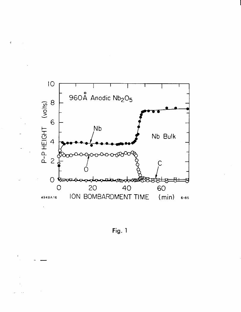
.4.2 SPUTTER ETCH PROFILES
Anodic Nb2 05 :
Auger spectra for sputter etch profiles were taken with Ar gas in the sys-
tem and the ion beam off. Calibration of Ar ion sputter etch rates of NbzOs
was accomplished using anodically prepared coatings of various thicknesses
over the range of 96 A to 5400 A. X-ray diffraction measurements on the thick-
est film confirmed that it was single phase Nb20s. A typical sputter etch pro- -- file is shown in Figure 1 and the sputter etch calibration curve is shown in Fig-
ure 2. The ion bombardment time to the NbzOs/Nb interface is determined as
7

I
the time necessary for the average oxygen concentration in the Nb205 film to
fall 50% at the NbzOs/Nb interface. The calculated etch rate is approximately
320 A.mA.cmm2 .min- 1 for the conditions specified in Sec. 2
The profile of Figure 1 shows a small C buildup at the NbzOs/Nb inter-
face. The origin of this C is presumably due to air-borne contamination of the
freshly etched Nb surface prior to anodization. Some of this C persists into the
Nb bulk during sputtering. This effect is probably due to a combination of:
1) knock-on effects, 2) recontamination of the very active Nb surface with C-
containing molecules from the gas phase and 3) the very low sputtering yield of
C (which leads to surface segregation of the low-sputter-yield component).(15)
The C concentration analyzed for our bulk Nb samples was <30 ppm.
._ Powder Samples:
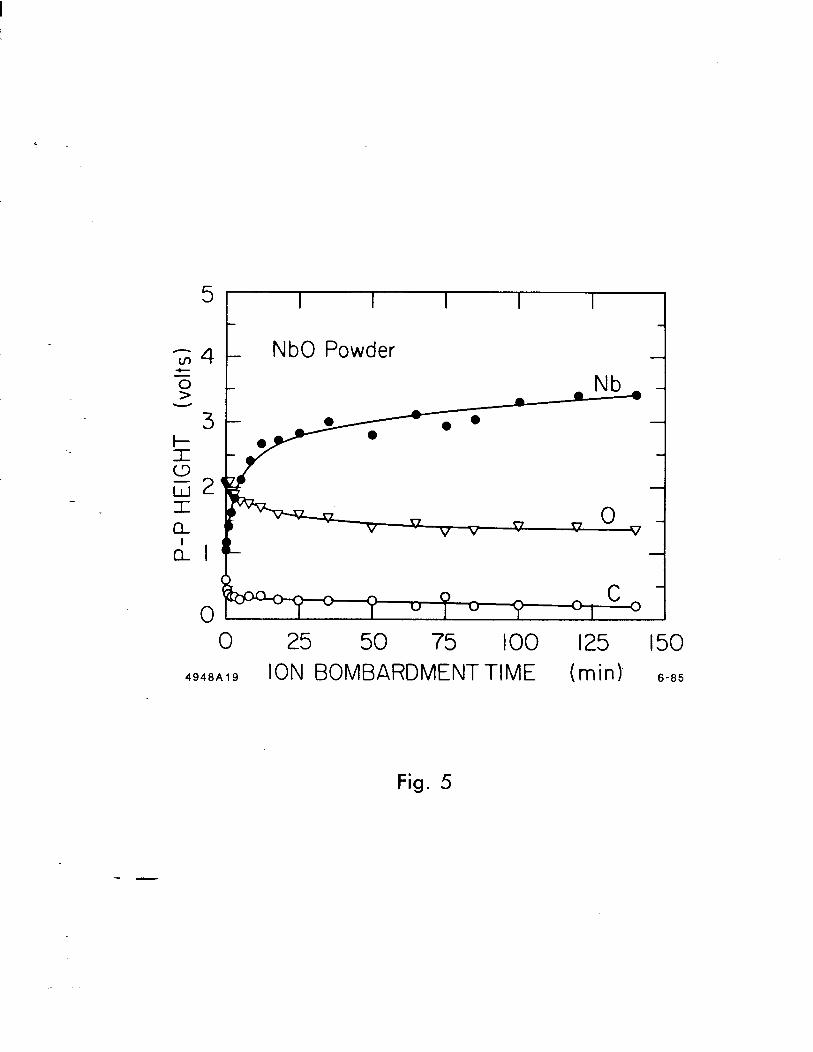
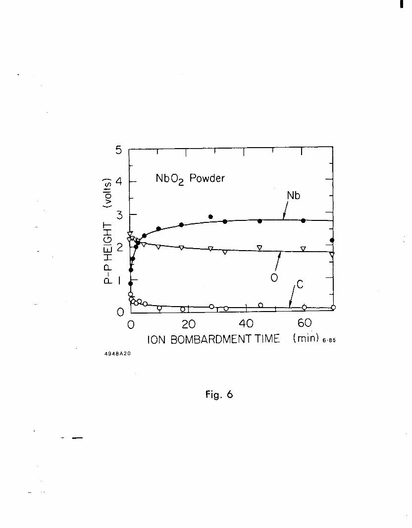
Depth profiles of the various powders studied in this work are shown in
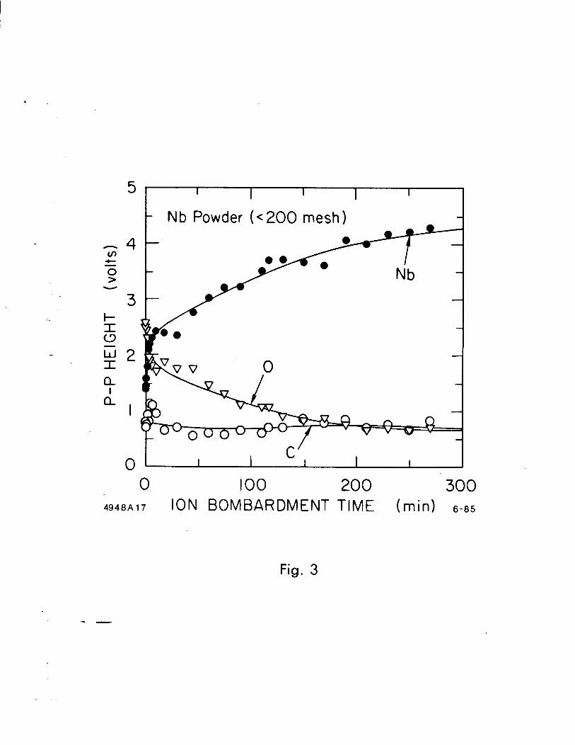
Figures 3-9. The 0 and C content is high, as expected, in the highly reactive
Nb powder. The NbC and NbN samples are somewhat oxidized as well, even
after sputtering. These effects suggest that the results for powders presented
here may be indicative of, but certainly not identical to, data for solid mate- -.
rial.
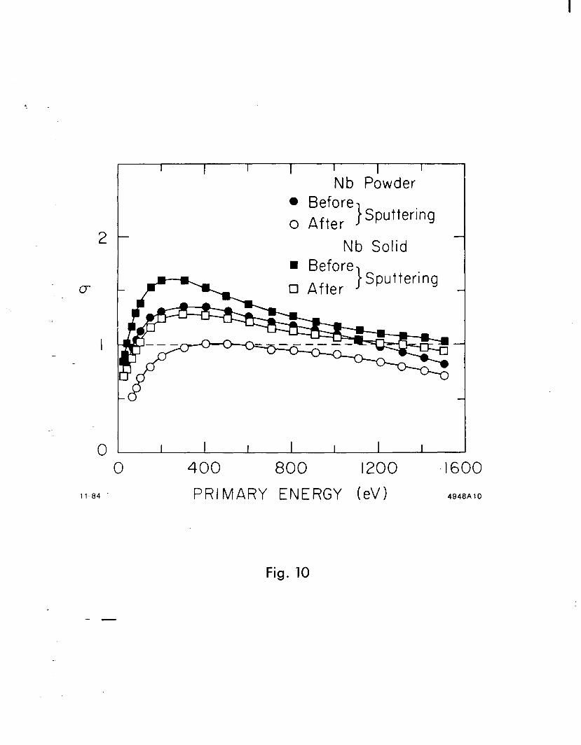
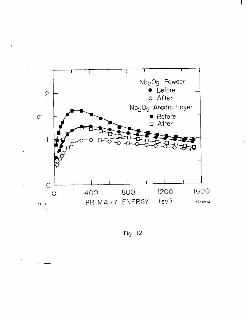
4.3 SECONDARYELECTRON YIELDS
Total secondary electron yield data for the various solid and powder sam-
ples is presented in Figures 10-13. The “before sputtering” curves are for sam-
ples as-inserted into vacuum, while those “after sputtering” represent the point
at which no further significant change in o could be observed with further
sputtering.
These equilibrium CT values were generally reached after short ion bombard- -- ment times of l-10 minutes (3 x 10 l6 to -3 x 10¹⁷ ions-cmm2),and reflect the
fact that the layer removed was probably the atmospheric contamination layer
8

present on the samples before insertion into vacuum. With continued sputter-
ing, the yield values remained quite constant although the Auger spectra con-
tinued to change during removal of the remaining lo-20% of a monolayer or so
of C and other contaminants in the case of anodized Nb205.
Figure 14 shows the results of o measurements made on anodized Nb205
at various stages of sputtering. The large change in Q upon removal of at-
mospheric contamination is quite evident, as well as its essentially unchanged
value when the bulk of the Nb205 is probed. As one sputters into the pure Nb
layer, there is a substantial rise in the high energy portion of the curve which
reflects an increase in the backscatter contribution to the yield. However, for
energies below 300 eV, there is little difference between the yields of clean Nb
and clean anodized NbzOs.
Measurements on Nb and NbzOs powders show Q values which are 20-30%
lower than for the corresponding solid materials. This can be attributed to
trapping of the secondary electrons in the powder matrix.(16) It is this mor-
phologically produced effect which probably produces the flat yield in powders
after removal of the atmospheric contamination layer.
4.4 STOICHIOMETRY
Figure 15 shows a portion of typical Auger spectra for a sputterlcleaned
anodic Nb205 layer on Nb, both before and after sputtering through the an-
odic layer. There are some obvious changes in the peak structure which might
be correlated with the chemical state of the Nb and then used to identify the
presence of various Nb-oxide compounds on technical cavity surfaces.
Lin and Licthman(7) have shown that the “doublet” structure of Figure
15 is due to “oxide” and “metal” peaks in those transitions having final state
Auger emissions in the Nb valence band. The doubling is obvious in the va- -- lence band transitions of Figure 15 while only small effects and no obvious dou-
bling is observed in the lower lying (higher binding energy) transitions.
9

If the “metal” and “oxide” components of the valence doublets were suf-
ficiently well separated in energy, an attempt could be made to correlate Nb
peak heights with oxygen/Nb concentration or oxidation number(17). Such a
correlation is sometimes done in XPS where the core levels used are usually
narrow and well resolved(18). The situation for Auger spectra, at least in the
Nb case, is very different. The line widths are 5-10 eV wide because of a com-
bination of the broad final state valence band emission energy broadening due
to short Auger transition times. Thus the distinct identity of the “oxide” and
“metal” peaks is (due to overlap) not preserved for analysis. Electron and ion
beam-induced decomposition of the surface oxides also act to further compli-
cate the situation, separately from the line width consideration. The sputter
profiles presented here use the total Nb transition at 170eV (including both
“metal” and “oxide” components) because of the difficulty in separating the
components.
While the presence of the doublets does provide a qualitative indication
that Nb oxides do exist on the surface, monitoring the Auger oxygen peak is a
simpler way of detecting oxygen on the surface.
5. Discussion
According to the literature, sputtering of Nb oxide surfaces apparently
leads to a reduction in the oxide state, Nb205 and NbOz reduce to Nb0(1g-21)
and NbO reduces to NbOo.7(21). Th e range of O/Nb of these sputtered surfaces
of 0.7 to 1.0 is in conflict with our results, as discussed below.
Examination of the depth profiles of Figures 5, 6 and 7 shows that the
sputtering time required to achieve equilibrium for the Nb oxide powders is in
the order tNb0 > tNb& > tj’,&&. This is not an oxide-state dependence but,
rather is due to the grazing incidence angle of the sputtering beam to the pow- -- der surfaces which cleans up larger particle size (see Table I) slower because of
shadowing effects.
10
Of more interest is the O/Nb ratio for these materials after having been
sputtered to equilibrium: 0.9 for Nb205, 0.7 for NbO2 and 0.4 for NbO. These
are in the same ratio as the O/Nb stoichiometry, namely, 0.9 : 0.7 : 0.4 as 2.5 :
2 : 1 for Nb205 : NbO2 : NbO. This range of 2.5 : 1 for O/Nb is very different
from that of 1 : 0.7 discussed above from the literature.
We believe that this disagreement is due to the depth of penetration of the
incident ions(22). An estimate(23) of the inelastic mean free path for 0 and
Nb Auger electrons from inorganic compounds is 20 and 11 A, respectively,
for the analyzed energies used here. However, a calculation of the penetration
depth of our ion beam using LSS theory(24-26), with an average atomic mass
for Nb205 equal to 38, yields a value of 12%1 at normal incidence and 4A at
the grazing incidence used here. So it is possible that the actual ion-damaged
layer of NbO, is very thin and contributes significantly less to the Auger in-
tensity in our spectra as compared to sputter-reduction studies previously
published(1g-21), simply because the ion beam is at grazing incidence and low
energy.
As a function of surface roughness, there is expected to be no dependence(27) -. of the O/Nb ratio for a given compound. merely as a function of surface
roughness(27). Absolute intensity however, should decrease as the roughness
increases and, indeed, the individual 0 and Nb signals of the smooth anodized
Nb20s layer of Figure 1 are larger than those of the powdered Nb205 sample
of Figure 7.
--
11

6. Conclusion
The measurements reported here were followed by studies on sputter-
deposited metalloids (TiN, Tic, NbN, NbC) conducted with more sophisti-
cated equipment using very low probe currents, pulse counting techniques and
dedicated computer manipulation of data(28). The present measurements do
indicate considerable promise of achieving Nb surfaces with low secondary elec-
tron emission. NbN and NbC look especially promising in this regard. We esti-
mate that perhaps 20-25010 of the secondary electrons are trapped by the pow-
ders, which implies that values close to unity should be achievable with solid
NbC and NbN. TiN is routinely used at SLAC (because of its relatively low
secondary electron yield) to coat various rf components for vacuum use.(2g)
--
12

7. References
1. J.P. Turneaure and I. Weissman, J. Appl. Phys. 39, 4417 (1968).
2. P. Kneisel, 0. Stoltz and J. Halbritter, J. Appl. Phys. 44, 1785 (1973).
3. I. Ben-Zvi, J.F. Crawford and J.P. Turneaure, IEEE Trans. Nucl. Sci.
54( 1973). NS-20,
4. Ph. Bernard, G. Cavallari, E. Chiaveri, E. Haebel, H. Heinrichs,
H. Lengeler, E. Picasso, V. Piciarelli and J. Tueckmantel, Nucl. In-
strum. Meth. 190, 257 (1981); Ph. Bernard, G. Cavallari, E. Chi-
averi, E. Haebel, H. Lengeler, H. Padamsee, V. Picciarelli, D. Proch, A.
Schwettman, J. Tiickmantel, W. Weingarten and H. Piel, Nucl. Instrum.
Meth. 206, 47(1983).
5. H. Lengeler, W. Weingarten, G. Miiller and H. Piel, IEEE Trans. on
Magnetics 2l, 1014 (1985); H. P a d amsee, IEEE Trans. on Magnetics 2l,
149 (1985).
6. T. Furuya, S. Hiramatsu, T. Nakazato, T. Kato, P. Kneisel, Y. Kojima
and T. Takagi, IEEE Trans. Nucl. Sci. NS-28, 3225(1981).
7. T.T. Lin and D. Lichtman, J. Mat. Sci. l4, 455 (1979).
8. Hydrogenous impurity protection alloy. Vallecitos Nuclear Center, Gen-
eral Electric Co.
9. Varian Cylindrical Mirror Analyzer Model 981-2067, Varian Ion Bom-
bardment Gun Model 981-2046.
10. V.E. Henrich, Rev. Sci. Instrum. 45, 861(1974).
11. C.G. Pantano and T.E. Madey, Appl. Surf. Sci., 2, 115(1981).
12. Y.L. Chiou, Thin Solid Films, 8, R37(1971).
13. T.W. Hickmott, J. Appl. Phys., 37, 4380 (1966).
13

14. L.C. Davis, N.C. MacDonald, P. W. Palmberg, G.E. Riach and R.E. We-
ber, Handbook of Auger Electron Spectroscopy, 2nd Ed., PHI Industries
(1976).
15. G. Betz and G.K. Wehner, in: Sputtering by Particle Bombardment II, R.
Behrisch, ed., Springer-Verlag, New York (1983).
16. S. Fliigge, Hundbuch der Physik, Vol. XXI, 261, Springer-Verlag, Heidel-
berg( 1956).
17. C.R. Brundle, Surface Sci. 52, 426 (1975); F.J. Szalkowski and G.A. So-
morjai, J. Chem. Phys. 56, 6097 (1972); F.J. Szalkowski and G.A. So-
morjai, Surface Sci. 52, 431(1975).
18. M.K. Bahl, J. Phys. Chem. Solids 36, 485(1975).
19. D.K. Murti and Roger Kelly, Thin Solid Films 33, 149(1976).
20. M. Grundner and J. Halbritter, J. Appl. Phys. 5l, 397(1980).
21. P.C. Karulkar, J. Vat. Sci. Technol. 18 169(1981).
22. P.H. Holloway and R.S. Bhattacharya, Surf. Interface Anal. 3, 118(1981).
23. M.P. Seah and W.A. Dench, Surf. Interface Anal. 1, 2(1979).
24. H.E. Schiott, Rad. Eff. 6, 107(1970).
25. P. Sigmund and J.B. Sanders, Int. Conf. on Appl. of Ion Beams to Semi-
conductor Technology, Grenoble, 1967.
26. M.A. Taubenblatt and C.R. Helms, J. Appl. Phys. 54, 2667(1983).
27. O.K.T. Wu and E.M. Butler, J. Vat. Sci. Technol. 20, 453(1982).
28. To be submitted for publication.
29. I.E. Campisi, H. Deruyter, Z.D. Farkas, E.L. Garwin, H.A. Hogg, F. King
and R.E. Kirby, IEEE Trans. Nucl. Sci., NS - 30, 3363(1983).
14

8. Figure Captions
1. Typical sputter profile of 960 A anodic Nb205. The Nb peak monitored
is the total M4,5N2,3V transition (both oxide and metal components at
-170eV).
2. Sputter calibration curve for anodic Nb 2 0 5. Non-zero vertical axis inter-
cept due to presence of surface contamination on as-inserted films, e.g.
see Figure 1.
3. Sputter profile for <200 mesh Nb powder.
4. Sputter profile for >48 mesh Nb powder.
5. Sputter profile for NbO powder.
6. Sputter profile for NbO2 powder.
7. Sputter profile for Nb205 powder.
8. Sputter profile for NbC powder.
9. Sputter profile for NbN powder.
-. 10. Secondary electron emission yield for >48 mesh Nb powder and solid Nb.
11. Secondary electron emission yield for NbO and NbO2 powders.
12. Secondary electron emission yield for Nb205 powder and anodic layer.
.13. Secondary electron emission yield for NbC and NbN powders. Yield of
polycrystalline graphite shown for comparison.
14. Secondary electron emission yield while sputtering through an 1lOOA an-
odized Nb205 layer into the underlying Nb bulk: o-as inserted, x-30 set
sputtering, o-22 min sputtering, v-53.5 min sputtering (interface), c-250
min sputtering (Nb bulk).
- 45. Auger transitions for clean anodized Nb205 and Nb.
15
T (3 w4 I
-. 0 0 20 40 60
4948A16 ION BOMBARDMENT TIME (min) 6-85
Fig. 1
--

800
600
400
I I I - 0 0 to 20 30 40 50
lo-84 . 4948A2 ION BOMBARDMENT TIME (mid
Fig. 2
--
5
‘3; 4 5
-3 t- 3 F2 a, I n I
-.
0
I I I I I I
t Nb Powder (~200 mesh) -I .0/6=9-l - w
8
I I C’ I I
0 100 200 300 4948A17 ION BOMBARDMENT TIME (min) 6-85
Fig. 3
--

5 - I I I I I I I
- Nb Powder (>48 mesh) 0 .- .
CilF “- V V
r\ u
h ” U ” v 0
0 I I I I
0 50 100 150 200 4948A18 ION BOMBARDMENT TIME (min). 6-85
Fig. 4
--
5
0 0 25 50 75 100 125 150
4946A19 ION BOMBARDMENTTIME (mink 6-65
Fig. 5
--
I
5
- 3
l- 3 w2 I CL
0
Nb
0 20 40 60 ION BOMBARDMENT TIME hid 6-85
4948A20
Fig. 6
--

I
i
I I I I I I
_ Nb,O, Powder
Nb 0 0
0 2 6 6-85 4948A2 1 ION BOMBARDMENT TIME (min)
Fig. 7
--

I
*
5
0
Nb I
0 20 40 60 4946A22 IoN BOMBARDMENT TIME (mi,d 6-85
Fig. 8
--

I
5
G4
I I I I I I I I I
- NbN Powder Nb I 3
0 0 20 40 60 80
4948A23 IoN BOMBARDMENT TIME ( mi!-d 6-85
Fig. 9
--
i
o-
Nb Powder l Before o After 1 Sputtering
Nb Solid
0 I I I I I I I
0 400 800 1200 .I600
11-84 . PRIMARY ENERGY (eV> 4940AlO
Fig. 10
--

2
0
I
0 0 400 800 1200 1600
11-84 PRIMARY ENERGY (eV) 4948All
I I I I I I I
NbO Powder Nb02 Powder l Before m Before o After o After
Fig. 11
--
I
2
0
Nb205 Powder l Before o After
Nb205 Anodic Layer l Before
I I I I I I I
I I I I I 1 I 1
0 11-84
400 800 1200 1600
PRIMARY ENERGY (ev ) 4948A12
Fig. 12

2
-. 0
11-84
I I I I I I I
NbC Powder - l Before
o After
- - - Graphite NbN Powder m Before
I I I I I I I
0 400 800 1200 1600
PRIMARY ENERGY (eV) 4948Al3
Fig. 13
--

Anodized NbzO,/Nb
I .6
1.2
o-
0.8
I I I I I I I I I I I I I I 1
0 0 200 400 600 800 1000 1200 1400 1600
PRIMARY ENERGY WI ,BnAb
Fig. 14
--
.

Sputter-Cleaned Anod. Nt
5-80
120 140 160 180 ELECTRON ENERGY
Fig. 15
200
(eW
240
3828A4
--