Embed Size (px)
Citation preview
CMOS SDRAMDEVICE OPERATIONS
ELECTRONICS
SDRAM Device Operations
* Samsung Electronics reserves the right to change products or specification without notice.

CMOS SDRAMDEVICE OPERATIONS
ELECTRONICS
A. MODE REGISTER FIELD TABLE TO PROGRAM MODES
Register Programmed with MRS
Address
Function
An ~ A10/AP
RFU
A9
W.B.L
A8 A7
TM
A6 A5 A4 A3 A2 A1 A0
CAS Latency BT Burst Length
A8 A7 A6 A5 A4 A3 A2 A1 A0 BT = 0
Test Mode
Type
Mode Register Set
Reserved
Reserved
Reserved
0
0
1
1
0
1
0
1
Write Burst Length
A9
0
1
Length
Burst
Single Bit
Latency
Reserved
Reserved
2
3
Reserved
Reserved
Reserved
Reserved
CAS Latency
0
0
0
0
1
1
1
1
0
0
1
1
0
0
1
1
0
1
0
1
0
1
0
1
Burst Type
0
1
BT = 1
Burst Length
Type
Sequential
Interleave
0
0
0
0
1
1
1
1
0
0
1
1
0
0
1
1
0
1
0
1
0
1
0
1
1
2
4
8
Reserved
Reserved
Reserved
Full Page
1
2
4
8
Reserved
Reserved
Reserved
Reserved
B. POWER UP SEQUENCE
1. Apply power and start clock, Attempt to maintain CKE= "H", DQM= "H" and the other pins are NOP condition at the inputs.2. Maintain stable power, stable clock and NOP input condition for a minimum of 200us.3. Issue precharge commands for all banks of the devices.4. Issue 2 or more auto-refresh commands.5. Issue a mode register set command to initialize the mode register. cf.) Sequence of 4 & 5 is regardless of the order.The device is now ready for normal operation.
Note : 1. If A9 is high during MRS cycle, "Burst Read Single Bit Write" function will be enabled. 2. RFU (Reserved for future use) should stay "0" during MRS cycle.
BA0 ~ BA1
RFU
* Full Page Length 64Mb : x4 (1024), x8 (512), x16 (256)128Mb : x4 (2048), x8 (1024), x16 (512)256Mb: x4 (2048), x8 (1024), x16 (512)

CMOS SDRAMDEVICE OPERATIONS
ELECTRONICS
C. BURST SEQUENCE
Initial AddressSequential Interleave
A1 A0
0
0
1
1
0
1
0
1
0
1
2
3
1
2
3
0
2
3
0
1
3
0
1
2
0
1
2
3
1
0
3
2
2
3
0
1
3
2
1
0
2. BURST LENGTH = 8
Initial AddressSequential Interleave
0
0
0
0
1
1
1
1
0
1
0
1
0
1
0
1
0
1
2
3
4
5
6
7
2
3
4
5
6
7
0
1
4
5
6
7
0
1
2
3
6
7
0
1
2
3
4
5
A1 A0A2
0
0
1
1
0
0
1
1
1
2
3
4
5
6
7
0
3
4
5
6
7
0
1
2
5
6
7
0
1
2
3
4
7
0
1
2
3
4
5
6
0
1
2
3
4
5
6
7
2
3
0
1
6
7
4
5
4
5
6
7
0
1
2
3
6
7
4
5
2
3
0
1
1
0
3
2
5
4
7
6
3
2
1
0
7
6
5
4
5
4
7
6
1
0
3
2
7
6
5
4
3
2
1
0
1. BURST LENGTH = 4

CMOS SDRAMDEVICE OPERATIONS
ELECTRONICS
BANK ADDRESSES (BA0 ~ BA1)
: In case x 4
This SDRAM is organized as four independent banks of
4,194,304 words x 4 bits memory arrays. The BA0 ~ BA1 inputs
are latched at the time of assertion of RAS and CAS to select the
bank to be used for the operation. The bank addresses BA0 ~ BA1
are latched at bank active, read, write, mode register set and pre-
charge operations.
: In case x 8
This SDRAM is organized as four independent banks of
2,097,152 words x 8 bits memory arrays. The BA0 ~ BA1 inputs
are latched at the time of assertion of RAS and CAS to select the
bank to be used for the operation. The bank addresses BA0 ~ BA1
are latched at bank active, read, write, mode register set and pre-
charge operations.
: In case x 16
This SDRAM is organized as four independent banks of
1,048,576 words x 16 bits memory arrays. The BA0 ~ BA1 inputs
are latched at the time of assertion of RAS and CAS to select the
bank to be used for the operation. The bank addresses BA0 ~ BA1
are latched at bank active, read, write, mode register set and pre-
charge operations.
ADDRESS INPUTS (A0 ~ A11): In case x 4
The 22 address bits are required to decode the 4,194,304 word
locations are multiplexed into 12 address input pins (A0 ~ A11).
The 12 bit row addresses are latched along with RAS and BA0 ~
BA1 during bank activate command. The 10 bit column addresses
are latched along with CAS, WE and BA0 ~ BA1 during read or
write command.
: In case x 8
The 21 address bits are required to decode the 2,097,152 word
locations are multiplexed into 12 address input pins (A0 ~ A11).
The 12 bit row addresses are latched along with RAS and BA0 ~
BA1 during bank activate command. The 9 bit column addresses
are latched along with CAS, WE and BA0 ~ BA1 during read or
write command.
: In case x 16
The 20 address bits are required to decode the 1,048,576 word
locations are multiplexed into 12 address input pins (A0 ~ A11).
The 12 bit row addresses are latched along with RAS and BA0 ~
BA1 during bank activate command. The 8 bit column addresses
are latched along with CAS, WE and BA0 ~ BA1 during read or
write command.
ADDRESSES of 64Mb
D. DEVICE OPERATIONS
BANK ADDRESSES (BA0 ~ BA1)
: In case x 4
This SDRAM is organized as four independent banks of
8,388,608 words x 4 bits memory arrays. The BA0 ~ BA1 inputs
are latched at the time of assertion of RAS and CAS to select the
bank to be used for the operation. The bank addresses BA0 ~ BA1
are latched at bank active, read, write, mode register set and pre-
charge operations.
: In case x 8
This SDRAM is organized as four independent banks of
4,194,304 words x 8 bits memory arrays. The BA0 ~ BA1 inputs
are latched at the time of assertion of RAS and CAS to select the
bank to be used for the operation. The bank addresses BA0 ~ BA1
are latched at bank active, read, write, mode register set and pre-
charge operations.
: In case x 16
This SDRAM is organized as four independent banks of
2,097,152 words x 16 bits memory arrays. The BA0 ~ BA1 inputs
are latched at the time of assertion of RAS and CAS to select the
bank to be used for the operation. The bank addresses BA0 ~ BA1
are latched at bank active, read, write, mode register set and pre-
charge operations.
ADDRESS INPUTS (A0 ~ A11)
: In case x 4
The 23 address bits are required to decode the 8,388,608 word
locations are multiplexed into 12 address input pins (A0 ~ A11).
The 12 bit row addresses are latched along with RAS and BA0 ~
BA1 during bank activate command. The 11 bit column addresses
are latched along with CAS, WE and BA0 ~ BA1 during read or
write command.
: In case x 8
The 22 address bits are required to decode the 4,194,304 word
locations are multiplexed into 12 address input pins (A0 ~ A11).
The 12 bit row addresses are latched along with RAS and BA0 ~
BA1 during bank activate command. The 10 bit column addresses
are latched along with CAS, WE and BA0 ~ BA1 during read or
write command.
: In case x 16
The 21 address bits are required to decode the 2,097,152 word
locations are multiplexed into 12 address input pins (A0 ~ A11).
The 12 bit row addresses are latched along with RAS and BA0 ~
BA1 during bank activate command. The 9 bit column addresses
are latched along with CAS, WE and BA0 ~ BA1 during read or
write command.
ADDRESSES of 128Mb

CMOS SDRAMDEVICE OPERATIONS
ELECTRONICS
BANK ADDRESSES (BA0 ~ BA1)
: In case x 4
This SDRAM is organized as four independent banks of
16,777,216 words x 4 bits memory arrays. The BA0 ~ BA1 inputs
are latched at the time of assertion of RAS and CAS to select the
bank to be used for the operation. The bank addresses BA0 ~ BA1
are latched at bank active, read, write, mode register set and pre-
charge operations.
: In case x 8
This SDRAM is organized as four independent banks of
8,388,608 words x 8 bits memory arrays. The BA0 ~ BA1 inputs
are latched at the time of assertion of RAS and CAS to select the
bank to be used for the operation. The bank addresses BA0 ~ BA1
are latched at bank active, read, write, mode register set and pre-
charge operations.
: In case x 16
This SDRAM is organized as four independent banks of
4,194,304 words x 16 bits memory arrays. The BA0 ~ BA1 inputs
are latched at the time of assertion of RAS and CAS to select the
bank to be used for the operation. The bank addresses BA0 ~ BA1
are latched at bank active, read, write, mode register set and pre-
charge operations.
ADDRESS INPUTS (A0 ~ A12)
: In case x 4
The 24 address bits are required to decode the 16,777,216 word
locations are multiplexed into 13 address input pins (A0 ~ A12).
The 13 bit row addresses are latched along with RAS and BA0 ~
BA1 during bank activate command. The 11 bit column addresses
are latched along with CAS, WE and BA0 ~ BA1 during read or
write command.
: In case x 8
The 23 address bits are required to decode the 8,388,608 word
locations are multiplexed into 13 address input pins (A0 ~ A12).
The 13 bit row addresses are latched along with RAS and BA0 ~
BA1 during bank activate command. The 10 bit column addresses
are latched along with CAS, WE and BA0 ~ BA1 during read or
write command.
: In case x 16
The 22 address bits are required to decode the 4,194,304 word
locations are multiplexed into 13 address input pins (A0 ~ A12).
The 13 bit row addresses are latched along with RAS and BA0 ~
BA1 during bank activate command. The 9 bit column addresses
are latched along with CAS, WE and BA0 ~ BA1 during read or
write command.
ADDRESSES of 256Mb
D. DEVICE OPERATIONS (continued)
CLOCK (CLK)The clock input is used as the reference for all SDRAM opera-
tions. All operations are synchronized to the positive going edge
of the clock. The clock transitions must be monotonic between VIL
and VIH. During operation with CKE high all inputs are assumed to
be in a valid state (low or high) for the duration of set-up and hold
time around positive edge of the clock in order to function well Q
perform and ICC specifications.
CLOCK ENABLE (CKE)The clock enable(CKE) gates the clock onto SDRAM. If CKE goes
low synchronously with clock (set-up and hold time are the same
as other inputs), the internal clock is suspended from the next
clock cycle and the state of output and burst address is frozen as
long as the CKE remains low. All other inputs are ignored from the
next clock cycle after CKE goes low. When all banks are in the
idle state and CKE goes low synchronously with clock, the
SDRAM enters the power down mode from the next clock cycle.
The SDRAM remains in the power down mode ignoring the other
inputs as long as CKE remains low. The power down exit is syn-
chronous as the internal clock is suspended. When CKE goes
high at least "1CLK + tSS" before the high going edge of the clock,
then the SDRAM becomes active from the same clock edge
accepting all the input commands.
NOP and DEVICE DESELECTWhen RAS, CAS and WE are high, the SDRAM performs no
operation (NOP). NOP does not initiate any new operation, but is
needed to complete operations which require more than single
clock cycle like bank activate, burst read, auto refresh, etc. The
device deselect is also a NOP and is entered by asserting CS
high. CS high disables the command decoder so that RAS, CAS,
WE and all the address inputs are ignored.

CMOS SDRAMDEVICE OPERATIONS
ELECTRONICS
DQM OPERATION
The DQM is used to mask input and output operations. It works
similar to OE during read operation and inhibits writing during
write operation. The read latency is two cycles from DQM and
zero cycle for write, which means DQM masking occurs two
cycles later in read cycle and occurs in the same cycle during
write cycle. DQM operation is synchronous with the clock. The
DQM signal is important during burst interruptions of write with
read or precharge in the SDRAM. Due to asynchronous nature of
the internal write, the DQM operation is critical to avoid unwanted
or incomplete writes when the complete burst write is not
required. Please refer to DQM timing diagram also.
MODE REGISTER SET (MRS)The mode register stores the data for controlling the various oper-
ating modes of SDRAM. It programs the CAS latency, burst type,
burst length, test mode and various vendor specific options to
make SDRAM useful for variety of different applications. The
default value of the mode register is not defined, therefore the
mode register must be written after power up to operate the
SDRAM. The mode register is written by asserting low on CS,
RAS, CAS and WE (The SDRAM should be in active mode with
CKE already high prior to writing the mode register). The state of
address pins A0 ~ An and BA0 ~ BA1 in the same cycle as CS,
RAS, CAS and WE going low is the data written in the mode reg-
ister. Two clock cycles is required to complete the write in the
mode register. The mode register contents can be changed using
the same command and clock cycle requirements during opera-
tion as long as all banks are in the idle state. The mode register is
divided into various fields depending on the fields of functions.
The burst length field uses A0 ~ A2, burst type uses A3, CAS
latency (read latency from column address) use A4 ~ A6, vendor
specific options or test mode use A7 ~ A8, A10/AP ~ An and BA0 ~
BA1. The write burst length is programmed using A9. A7 ~ A8, A10/
AP ~ An and BA0 ~ BA1 must be set to low for normal SDRAM
operation. Refer to the table for specific codes for various burst
length, burst type and CAS latencies.
D. DEVICE OPERATIONS (continued)
BANK ACTIVATE
The bank activate command is used to select a random row in an
idle bank. By asserting low on RAS and CS with desired row and
bank address, a row access is initiated. The read or write opera-
tion can occur after a time delay of tRCD(min) from the time of
bank activation. tRCD is an internal timing parameter of SDRAM,
therefore it is dependent on operating clock frequency. The mini-
mum number of clock cycles required between bank activate and
read or write command should be calculated by dividing tRCD(min)
with cycle time of the clock and then rounding off the result to the
next higher integer. The SDRAM has four internal banks in the
same chip and shares part of the internal circuitry to reduce chip
area, therefore it restricts the activation of four banks simulta-
neously. Also the noise generated during sensing of each bank of
SDRAM is high, requiring some time for power supplies to recover
before another bank can be sensed reliably. tRRD(min) specifies
the minimum time required between activating different bank. The
number of clock cycles required between different bank activation
must be calculated similar to tRCD specification. The minimum
time required for the bank to be active to initiate sensing and
restoring the complete row of dynamic cells is determined by
tRAS(min). Every SDRAM bank activate command must satisfy
tRAS(min) specification before a precharge command to that
active bank can be asserted. The maximum time any bank can be
in the active state is determined by tRAS(max). The number of
cycles for both tRAS(min) and tRAS(max) can be calculated similar
to tRCD specification.
BURST READ
The burst read command is used to access burst of data on con-
secutive clock cycles from an active row in an active bank. The
burst read command is issued by asserting low on CS and CAS
with WE being high on the positive edge of the clock. The bank
must be active for at least tRCD(min) before the burst read com-
mand is issued. The first output appears in CAS latency number
of clock cycles after the issue of burst read command. The burst
length, burst sequence and latency from the burst read command
is determined by the mode register which is already programmed.

CMOS SDRAMDEVICE OPERATIONS
ELECTRONICS
The burst read can be initiated on any column address of the
active row. The address wraps around if the initial address does
not start from a boundary such that number of outputs from each
I/O are equal to the burst length programmed in the mode regis-
ter. The output goes into high-impedance at the end of the burst,
unless a new burst read was initiated to keep the data output gap-
less. The burst read can be terminated by issuing another burst
read or burst write in the same bank or the other active bank or a
precharge command to the same bank. The burst stop command
is valid at every page burst length.
BURST WRITE
The burst write command is similar to burst read command and is
used to write data into the SDRAM on consecutive clock cycles in
adjacent addresses depending on burst length and burst
sequence. By asserting low on CS, CAS and WE with valid col-
umn address, a write burst is initiated. The data inputs are pro-
vided for the initial address in the same clock cycle as the burst
write command. The input buffer is deselected at the end of the
burst length, even though the internal writing can be completed
yet. The writing can be completed by issuing a burst read and
DQM for blocking data inputs or burst write in the same or another
active bank. The burst stop command is valid at every burst
length. The write burst can also be terminated by using DQM for
blocking data and procreating the bank tRDL after the last data
input to be written into the active row. See DQM OPERATION
also.
ALL BANKS PRECHARGE
All banks can be precharged at the same time by using Precharge
all command. Asserting low on CS, RAS, and WE with high on
A10/AP after all banks have satisfied tRAS(min) requirement, per-
forms precharge on all banks. At the end of tRP after performing
precharge to all the banks, all banks are in idle state.
D. DEVICE OPERATIONS (continued)
PRECHARGE
The precharge operation is performed on an active bank by
asserting low on CS, RAS, WE and A10/AP with valid BA0 ~ BA1
of the bank to be precharged. The precharge command can be
asserted anytime after tRAS(min) is satisfied from the bank active
command in the desired bank. tRP is defined as the minimum
number of clock cycles required to complete row precharge is cal-
culated by dividing tRP with clock cycle time and rounding up to
the next higher integer. Care should be taken to make sure that
burst write is completed or DQM is used to inhibit writing before
precharge command is asserted. The maximum time any bank
can be active is specified by tRAS(max). Therefore, each bank
activate command. At the end of precharge, the bank enters the
idle state and is ready to be activated again. Entry to Power down,
Auto refresh, Self refresh and Mode register set etc. is possible
only when all banks are in idle state.
AUTO PRECHARGE
The precharge operation can also be performed by using auto
precharge. The SDRAM internally generates the timing to satisfy
tRAS(min) and "tRP" for the programmed burst length and CAS
latency. The auto precharge command is issued at the same time
as burst read or burst write by asserting high on A10/AP. If burst
read or burst write by asserting high on A10/AP, the bank is left
active until a new command is asserted. Once auto precharge
command is given, no new commands are possible to that partic-
ular bank until the bank achieves idle state.
AUTO REFRESH
The storage cells of 64Mb, 128Mb and 256Mb SDRAM need to be
refreshed every 64ms to maintain data. An auto refresh cycle
accomplishes refresh of a single row of storage cells. The internal
counter increments automatically on every auto refresh cycle to
refresh all the rows. An auto refresh command is issued by
asserting low on CS, RAS and CAS with high on CKE and WE.
The auto refresh command can only be asserted with both banks
being in idle state and the device is not in power down mode
(CKE is high in the previous cycle).

CMOS SDRAMDEVICE OPERATIONS
ELECTRONICS
SELF REFRESH
The self refresh is another refresh mode available in the SDRAM.
The self refresh is the preferred refresh mode for data retention
and low power operation of SDRAM. In self refresh mode, the
SDRAM disables the internal clock and all the input buffers except
CKE. The refresh addressing and timing are internally generated
to reduce power consumption.
The self refresh mode is entered from all banks idle state by
asserting low on CS, RAS, CAS and CKE with high on WE. Once
the self refresh mode is entered, only CKE state being low mat-
ters, all the other inputs including the clock are ignored in order to
remain in the self refresh mode.
The self refresh is exited by restarting the external clock and then
asserting high on CKE. This must be followed by NOP's for a mini-
mum time of tRC before the SDRAM reaches idle state to begin
normal operation. If the system uses burst auto refresh during nor-
mal operation, it is recommended to use burst 8192 auto refresh
cycles for 256Mb and burst 4096 auto refresh cycles for 128Mb
and 64Mb immediately after exiting in self refresh mode.
D. DEVICE OPERATIONS (continued)
The time required to complete the auto refresh operation is speci-
fied by tRC(min). The minimum number of clock cycles required
can be calculated by driving tRC with clock cycle time and them
rounding up to the next higher integer. The auto refresh command
must be followed by NOP's until the auto refresh operation is com-
pleted. All banks will be in the idle state at the end of auto refresh
operation. The auto refresh is the preferred refresh mode when
the SDRAM is being used for normal data transactions. The 64Mb
and 128Mb SDRAM’s auto refresh cycle can be performed once in
15.6us or a burst of 4096 auto refresh cycles once in 64ms. The
256Mb SDRAM’s auto refresh cycle can be performed once in
7.8us or a burst of 8192 auto refresh cycles once in 64ms.

CMOS SDRAMDEVICE OPERATIONS
ELECTRONICS
1) Clock Suspended During Write (BL=4)
1. CLOCK Suspend
WR
D0 D1 D2 D3
D0 D1 D2 D3
CLK
CMD
CKE
InternalCKE
DQ(CL2)
DQ(CL3)
Masked by CKE
2) Clock Suspended During Read (BL=4)
D0
Not Written
1) Write Mask (BL=4)
2. DQM Operation
WR
D0 D1 D3
D0 D1 D3
CLK
CMD
DQM
DQ(CL2)
DQ(CL3)
Masked byDQM
2) Read Mask (BL=4)
RD
Q0 Q2 Q3
Q1 Q2 Q3
Masked by DQM
DQM to Data-in Mask = 0 DQM to Data-out Mask = 2
Hi-Z
Hi-Z
3) DQM with Clock Suspended (Full Page Read) *2
RD
CLK
CMD
CKE
DQ(CL2)
DQ(CL3)
Q0 Q4 Q7 Q8Q2
Q3 Q6 Q7Q1
Hi-Z
Hi-Z
Hi-Z
Hi-Z
Hi-Z
Hi-Z
DQM
*Note : 1. CKE to CLK disable/enable = 1CLK.2. DQM makes data out Hi-Z after 2CLKs which should masked by CKE " L"3. DQM masks both data-in and data-out.
E. BASIC FEATURE AND FUNCTION DESCRIPTIONS
RD
Q0 Q1 Q2
Q0 Q1 Q2 Q3
Masked by CKE
Q3
Suspended Dout
Q6
Q5
CLK
CMD
CKE
InternalCKE
DQ(CL2)
DQ(CL3)
CLK
CMD
DQM
DQ(CL2)
DQ(CL3)

CMOS SDRAMDEVICE OPERATIONS
ELECTRONICS
1) Read interrupted by Read (BL=4) *1
3. CAS Interrupt (I)
CLK
CMD
ADD
RD RD
A B
QA0 QB1 QB2 QB3QB0
QA0 QB1 QB2 QB3QB0
tCCD *2
2) Write interrupted by Write (BL=2) 3) Write interrupted by Read (BL=2)
WR WR
A B
tCCD *2
DA0 DB1DB0
tCDL *3
CLK
CMD
ADD
DQ
WR RD
A B
tCCD *2
tCDL *3
DA0 QB1QB0
DA0 QB1QB0
DQ(CL2)
DQ(CL3)
*Note : 1. By " Interrupt", It is meant to stop burst read/write by external command before the end of burst. By "CAS Interrupt", to stop burst read/write by CAS access ; read and write.
2. tCCD : CAS to CAS delay. (=1CLK)
3. tCDL : Last data in to new column address delay. (=1CLK)
DQ(CL2)
DQ(CL3)
CLK
CMD
ADD

CMOS SDRAMDEVICE OPERATIONS
ELECTRONICS
4. CAS Interrupt (II) : Read Interrupted by Write & DQM
*Note : 1. To prevent bus contention, there should be at least one gap between data in and data out.
D1 D2
RD
D3
WR
D0
D1 D2 D3D0
D1 D2 D3D0
RD WR
RD WR
Hi-Z
Hi-Z
RD WR
Q0 D1 D2 D3D0*1
Hi-Z
(a) CL=2, BL=4
CLK
i) CMD
DQM
DQ
ii) CMD
DQM
DQ
iii) CMD
DQM
DQ
iv) CMD
DQM
DQ
(b) CL=3, BL=4
CLK
i) CMD
DQM
DQ D1 D2
RD
D3
WR
D0
D1 D2 D3D0
D1 D2 D3D0
RD WR
RD WR
D1 D2 D3D0
RD WR
RD WR
D1 D2 D3D0Hi-Z
ii) CMD
DQM
DQ
iii) CMD
DQM
DQ
iii) CMD
DQM
DQ
iv) CMD
DQM
DQ Q0*1
Hi-Z

CMOS SDRAMDEVICE OPERATIONS
ELECTRONICS
*Note : 1. To prevent bus contention, DQM should be issued which makes at least one gap between data in and data out.2. To inhibit invalid write, DQM should be issued.3. This precharge command and burst write command should be of the same bank, otherwise it is not precharge interrupt but only another bank precharge of four banks operation.
5. Write Interrupted by Precharge & DQM
6. Precharge
tRDL*1
2) Normal Read (BL=4)
CLK
CMD
DQ(CL2)
DQ(CL3)
RD PRE
Q0 Q1 Q2 Q3
Q0 Q1 Q2 Q3
1
2
*Note : 1. SAMSUNG can support tRDL=1CLK and tRDL=2CLK for all memory devices. SAMSUNG recommends tRDL=2 CLK.
2. Number of valid output data after row precharge : 1, 2 for CAS Latency = 2, 3 respectively.3. The row active command of the precharge bank can be issued after tRP from this point.
The new read/write command of other activated bank can be issued from this point. At burst read/write with auto precharge, CAS interrupt of the same bank is illegal4. tDAL defined Last data in to Active delay. SAMSUNG can support tDAL=1CLK+20ns and 2CLK+20ns ,recommends tDAL=2CLK+20ns.
7. Auto Precharge
D0 D1 D2
CLK
CMD
DQ
WR
D3
1) Normal Write (BL=4) 2) Normal Read (BL=4)
CLK
CMD
DQ(CL2)
DQ(CL3)
RD
Q0 Q1 Q2 Q3
Q0 Q1 Q2 Q3
Auto Precharge Starts *3
*2
D0 D1 D2
CLK
CMD
DQM
DQ
Masked by DQM
WR PRE*3
*2
1) tRDL = 1 CLK 2) tRDL = 2CLK
Auto Precharge Starts @tRDL=1CLK *3
Auto Precharge Starts@tRDL=2CLK *3
D0 D1 D2
CLK
CMD
DQ
WR PRE
D3
1) Normal Write
BL=4 & tRDL=2CLK
D0 D1 D2
CLK
CMD
DQ
WR PRE
D3
BL=4 & tRDL=1CLK
tRDL*1
D0 D1 D2
CLK
CMD
DQM
DQ
Masked by DQM
WR PRE*3
*2
ACT
D0 D1 D2
CMD
DQ
WR
D3
ACT
tRDL =1CLK
tRDL =2CLK
tDAL =1CLK +20ns*4
tDAL =2CLK +20ns*4

CMOS SDRAMDEVICE OPERATIONS
ELECTRONICS
*Note : 1. SAMSUNG can support tRDL=1CLK and tRDL=2CLK for all memory devices. SAMSUNG recommends tRDL=2 CLK.
2. tBDL : 1 CLK ; Last data in to burst stop delay. Read or write burst stop command is valid at every burst length.3. Number of valid output data after row precharge or burst stop : 1, 2 for CAS latency= 2, 3 respectively. 4. PRE : All banks precharge is necessary. MRS can be issued only at all banks precharge state.
8. Burst Stop & Interrupted by Precharge
3) Read Interrupted by Precharge (BL=4)
CLK
CMD
DQ(CL2)
DQ(CL3)
RD PRE
Q0 Q1
Q0 Q1
1
2
9. MRS
CLK
PRE
1) Mode Register Set
4) Read Burst Stop (BL=4)
CLK
CMD
DQ(CL2)
DQ(CL3)
RD STOP
Q0 Q1
Q0 Q1
1
2
MRS ACT*4
tRP 2CLK
CMD
D0 D1 D2
CLK
CMD
DQ
WR PRE
1) Normal Write
tRDL*1
D0 D1 D2
CLK
CMD
DQ
WR STOP
D3
2) Write Burst Stop (BL=8)
DQM
DQM
tBDL *2
D0 D1 D2
CLK
CMD
DQ
WR PRE
tRDL*1
DQM
BL=4 & tRDL=1CLK BL=4 & tRDL=2CLK

CMOS SDRAMDEVICE OPERATIONS
ELECTRONICS
*Note : 1. Active power down : one or more banks active state.2. Precharge power down : all banks precharge state.3. The auto refresh is the same as CBR refresh of conventional DRAM. No precharge commands are required after auto refresh command. During tRC from auto refresh command, any other command can not be accepted.4. Before executing auto/self refresh command, all banks must be idle state.
5. MRS, Bank Active, Auto/Self Refresh, Power Down Mode Entry.6. During self refresh mode, refresh interval and refresh operation are performed internally. After self refresh entry, self refresh mode is kept while CKE is low. During self refresh mode, all inputs except CKE will be don't cared, and outputs will be in Hi-Z state. For the time interval of tRC from self refresh exit command, any other command can not be accepted. Before/After self refresh mode, burst auto refresh cycle (4096 cycles for 64Mb & 128Mb, 8192 cycles for 256Mb) is recommended.
10. Clock Suspend Exit & Power Down Exit
CLK
CKE
CMD RD
1) Clock Suspend (=Active Power Down) Exit
tSS
CLK
CKE
CMD
2) Power Down (=Precharge Power Down) Exit
*1
*5
InternalCLK
NOP
tSS
*2InternalCLK
11. Auto Refresh & Self Refresh
CLK
CMD
1) Auto Refresh
CKE
PRE AR CMD*4
tRP tRC
CLK
CMD
2) Self Refresh
CKE
PRE SR CMD*4
tRP tRC
Note 6
ACT
~~~~
~~~~
~~~~
~~
~~
CMOS SDRAMDEVICE OPERATIONS
ELECTRONICS
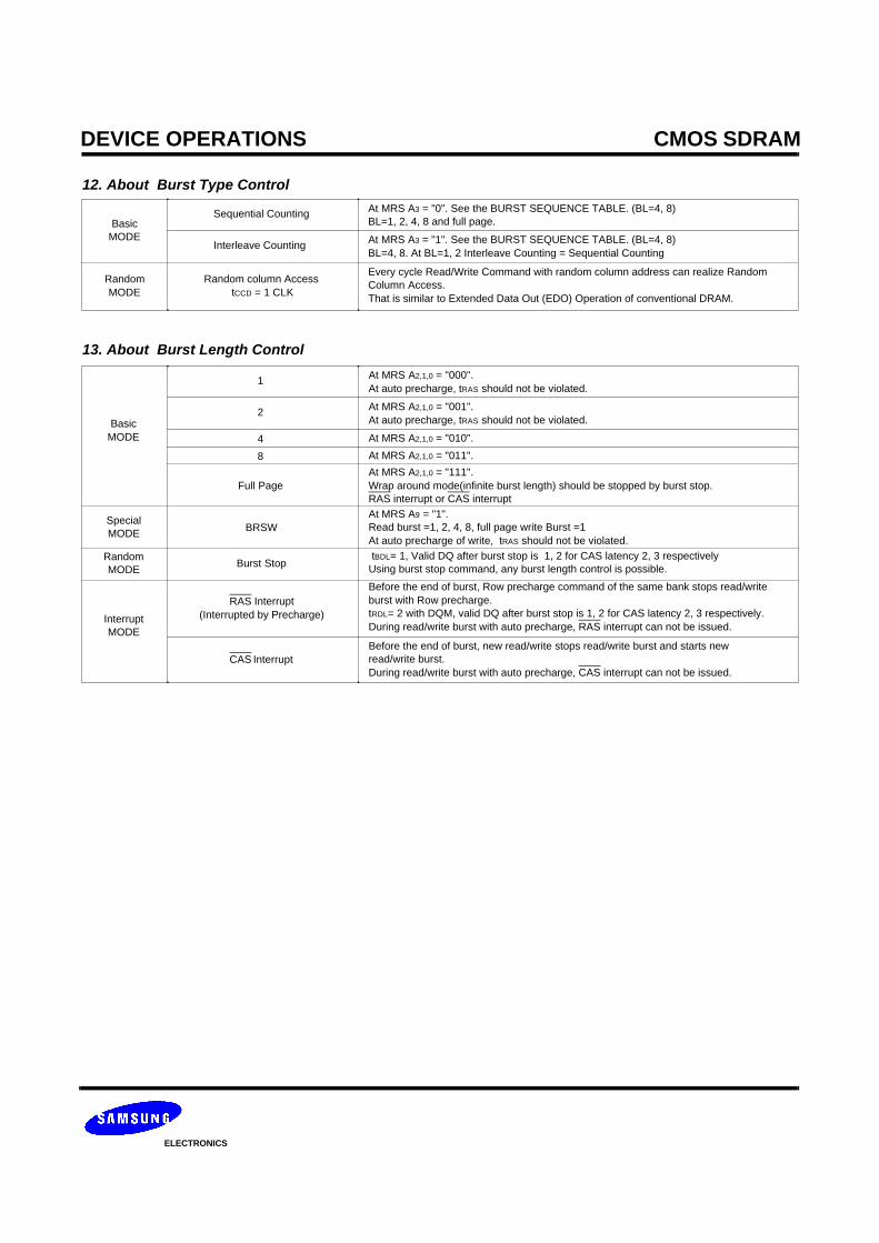
12. About Burst Type Control
At MRS A3 = "0". See the BURST SEQUENCE TABLE. (BL=4, 8)BL=1, 2, 4, 8 and full page.
At MRS A3 = "1". See the BURST SEQUENCE TABLE. (BL=4, 8)BL=4, 8. At BL=1, 2 Interleave Counting = Sequential Counting
Every cycle Read/Write Command with random column address can realize Random Column Access.That is similar to Extended Data Out (EDO) Operation of conventional DRAM.
BasicMODE
RandomMODE
Sequential Counting
Interleave Counting
Random column Access tCCD = 1 CLK
13. About Burst Length Control
At MRS A2,1,0 = "000". At auto precharge, tRAS should not be violated.
At MRS A2,1,0 = "001". At auto precharge, tRAS should not be violated.
Before the end of burst, Row precharge command of the same bank stops read/writeburst with Row precharge.tRDL= 2 with DQM, valid DQ after burst stop is 1, 2 for CAS latency 2, 3 respectively.During read/write burst with auto precharge, RAS interrupt can not be issued.
BasicMODE
InterruptMODE
1
2
RAS Interrupt (Interrupted by Precharge)
At MRS A2,1,0 = "010".
At MRS A2,1,0 = "011".
At MRS A2,1,0 = "111". Wrap around mode(infinite burst length) should be stopped by burst stop.RAS interrupt or CAS interrupt
4
8
Full Page
At MRS A9 = "1". Read burst =1, 2, 4, 8, full page write Burst =1At auto precharge of write, tRAS should not be violated. tBDL= 1, Valid DQ after burst stop is 1, 2 for CAS latency 2, 3 respectivelyUsing burst stop command, any burst length control is possible.
Before the end of burst, new read/write stops read/write burst and starts new read/write burst.During read/write burst with auto precharge, CAS interrupt can not be issued.
BRSW
Burst Stop
CAS Interrupt
RandomMODE
SpecialMODE

CMOS SDRAMDEVICE OPERATIONS
ELECTRONICS
X
X
X
CA, A10/AP
RA
A10/AP
X
OP code
X
X
X
CA, A10/AP
CA, A10/AP
RA
A10/AP
X
X
X
X
CA, A10/AP
CA, A10/AP
RA
A10/AP
X
X
X
X
CA, A10/AP
CA, A10/AP
RA
A10/AP
X
X
X
X
CA, A10/AP
RA, RA10
X
X
X
X
CA, A10/AP
RA, RA10
X
X
X
X
CA
RA
A10/AP
FUNCTION TRUTH TABLE (TABLE 1)
CurrentState
CS RAS CAS WE BA ADDR ACTION Note
H
L
L
L
L
L
L
L
H
L
L
L
L
L
L
L
H
L
L
L
L
L
L
L
H
L
L
L
L
L
L
L
H
L
L
L
L
L
H
L
L
L
L
L
H
L
L
L
L
L
IDLE
RowActive
Read
Write
Read withAuto
Precharge
Write withAuto
Precharge
Pre-charging
NOP
NOP
ILLEGAL
ILLEGAL
Row (& Bank) Active ; Latch RA
NOP
Auto Refresh or Self Refresh
Mode Register Access
NOP
NOP
ILLEGAL
Begin Read ; latch CA ; determine AP
Begin Write ; latch CA ; determine AP
ILLEGAL
Precharge
ILLEGAL
NOP (Continue Burst to End --> Row Active)
NOP (Continue Burst to End --> Row Active)
Term burst --> Row active
Term burst, New Read, Determine AP
Term burst, New Write, Determine AP
ILLEGAL
Term burst, Precharge timing for Reads
ILLEGAL
NOP (Continue Burst to End --> Row Active)
NOP (Continue Burst to End --> Row Active)
Term burst --> Row active
Term burst, New read, Determine AP
Term burst, New Write, Determine AP
ILLEGAL
Term burst, precharge timing for Writes
ILLEGAL
NOP (Continue Burst to End --> Precharge)
NOP (Continue Burst to End --> Precharge)
ILLEGAL
ILLEGAL
ILLEGAL
ILLEGAL
NOP (Continue Burst to End --> Precharge)
NOP (Continue Burst to End --> Precharge)
ILLEGAL
ILLEGAL
ILLEGAL
ILLEGAL
NOP --> Idle after tRP
NOP --> Idle after tRP
ILLEGAL
ILLEGAL
ILLEGAL
NOP --> Idle after tRP
X
X
X
BA
BA
BA
X
OP code
X
X
X
BA
BA
BA
BA
X
X
X
X
BA
BA
BA
BA
X
X
X
X
BA
BA
BA
BA
X
X
X
X
BA
BA
X
X
X
X
BA
BA
X
X
X
X
BA
BA
BA
X
H
H
H
L
L
L
L
X
H
H
H
H
L
L
L
X
H
H
H
H
L
L
L
X
H
H
H
H
L
L
L
X
H
H
H
L
L
X
H
H
H
L
L
X
H
H
H
L
L
X
H
H
L
H
H
L
L
X
H
H
L
L
H
H
L
X
H
H
L
L
H
H
L
X
H
H
L
L
H
H
L
X
H
H
L
H
L
X
H
H
L
H
L
X
H
H
L
H
H
X
H
L
X
H
L
H
L
X
H
L
H
L
H
L
X
X
H
L
H
L
H
L
X
X
H
L
H
L
H
L
X
X
H
L
X
X
X
X
H
L
X
X
X
X
H
L
X
H
L
2
2
4
5
5
2
2
3
2
3
3
2
3
2
2
2
2
2
4

CMOS SDRAMDEVICE OPERATIONS
ELECTRONICS
FUNCTION TRUTH TABLE (TABLE 1)CurrentState
CS RAS CAS WE BA ADDR ACTION Note
L
H
L
L
L
L
L
L
H
L
L
L
L
H
L
L
L
L
X
X
X
X
CA
RA
A10/AP
X
X
X
X
X
X
X
X
X
X
X
Row Activating
Refreshing
ILLEGAL
NOP --> Row Active after tRCD
NOP --> Row Active after tRCD
ILLEGAL
ILLEGAL
ILLEGAL
ILLEGAL
ILLEGAL
NOP --> Idle after tRC
NOP --> Idle after tRC
ILLEGAL
ILLEGAL
ILLEGAL
NOP --> Idle after 2 clocks
NOP --> Idle after 2 clocks
ILLEGAL
ILLEGAL
ILLEGAL
X
X
X
X
BA
BA
BA
X
X
X
X
X
X
X
X
X
X
X
L
X
H
H
H
L
L
L
X
H
H
L
L
X
H
H
H
L
L
X
H
H
L
H
H
L
X
H
L
H
L
X
H
H
L
X
X
X
H
L
X
H
L
X
X
X
X
X
X
X
H
L
X
X
2
2
2
2
Mode Register
Accessing
*Note : 1. All entries assume the CKE was active (High) during the precharge clock and the current clock cycle.2. Illegal to bank in specified state ; Function may be Iegal in the bank indicated by BA, depending on the state of that bank.3. Must satisfy bus contention, bus turn around, and/or write recovery requirements.4. NOP to bank precharging or in idle state. May precharge bank indicated by BA (and A10/AP).
5. Illegal if any bank is not idle.
Abbreviations : RA = Row Address BA = Bank Address NOP = No Operation Command CA = Column Address AP = Auto Precharge

CMOS SDRAMDEVICE OPERATIONS
ELECTRONICS
FUNCTION TRUTH TABLE (TABLE 2)
CurrentState
CS RAS CAS WE ADDR ACTION Note
X
H
L
L
L
L
X
X
H
L
L
L
L
X
X
H
L
L
L
L
L
L
X
X
X
X
X
X
X
X
X
X
X
X
X
X
X
X
X
X
X
X
X
X
X
X
RA
X
OP Code
X
X
X
X
X
SelfRefresh
INVALID
Exit Self Refresh --> Idle after tRFC (ABI)
Exit Self Refresh --> Idle after tRFC (ABI)
ILLEGAL
ILLEGAL
ILLEGAL
NOP (Maintain Self Refresh)
INVALID
Exit Power Down --> ABI
Exit Power Down --> ABI
ILLEGAL
ILLEGAL
ILLEGAL
NOP (Maintain Low Power Mode)
Refer to Table 1
Enter Power Down
Enter Power Down
ILLEGAL
ILLEGAL
Row (& Bank) Active
Enter Self Refresh
Mode Register Access
NOP
Refer to Operations in Table 1
Begin Clock Suspend next cycle
Exit Clock Suspend next cycle
Maintain Clock Suspend
X
X
H
H
H
L
X
X
X
H
H
H
L
X
X
X
H
H
H
L
L
L
X
X
X
X
X
X
X
H
H
L
X
X
X
X
H
H
L
X
X
X
X
H
H
L
H
L
L
X
X
X
X
X
X
X
H
L
X
X
X
X
X
H
L
X
X
X
X
X
H
L
X
H
H
L
X
X
X
X
X
6
6
7
7
8
8
8
9
9
AllBanks
Idle
*Note : 6. CKE low to high transition is asynchronous.7. CKE low to high transition is asynchronous if restarts internal clock. A minimum setup time 1CLK + tSS must be satisfied before any command other than exit.8. Power down and self refresh can be entered only from the both banks idle state.9. Must be a legal command.
Abbreviations : ABI = All Banks Idle, RA = Row Address
CKE(n-1)
H
L
L
L
L
L
L
H
L
L
L
L
L
L
H
H
H
H
H
H
H
H
L
H
H
L
L
X
H
H
H
H
H
L
X
H
H
H
H
H
L
H
L
L
L
L
L
L
L
L
H
L
H
L
CKEn
All Banks
PrechargePower Down
Any Stateother than
Listedabove

ELECTRONICS
TIMING DIAGRAM CMOS SDRAM
SDRAM Timing Diagram
* Samsung Electronics reserves the right to change products or specification without notice.

ELECTRONICS
TIMING DIAGRAM CMOS SDRAM
Single Bit Read - Write - Read Cycle(Same Page) @CAS Latency=3, Burst Length=1
Power Up Sequence
Read & Write Cycle at Same Bank @Burst Length=4, tRDL=1CLK
Read & Write Cycle at Same Bank @Burst Length=4, tRDL=2CLK
Page Read & Write Cycle at Same Bank @Burst Length=4, tRDL=1CLK
Page Read & Write Cycle at Same Bank @Burst Length=4, tRDL=2CLK
Page Read Cycle at Different Bank @Burst Length=4
Page Write Cycle at Different Bank @Burst Length=4, tRDL=1CLK
Page Write Cycle at Different Bank @Burst Length=4, tRDL=2CLK
Read & Write Cycle at Different Bank @Burst Length=4
Read & Write Cycle With Auto Precharge l @Burst Length=4
Read & Write Cycle With Auto Precharge ll @Burst Length=4
Clock Suspension & DQM Operation Cycle @CAS Letency=2, Burst Length=4
Read Interrupted by Precharge Command & Read Burst Stop Cycle @ Full Page Burst
Write Interrupted by Precharge Command & Write Burst Stop Cycle @ Full Page Burst, tRDL=1CLK
Write Interrupted by Precharge Command & Write Burst Stop Cycle @ Full Page Burst, tRDL=2CLK
Burst Read Single bit Write Cycle @Burst Length =2
Active/precharge Power Dower Down Mode @CAS Latency=2 Burst Length=4
Self Refresh Entry & Exit Cycle & Exit Cycle
Mode Register Set Cycle
Auto Refresh Cycle

TIMING DIAGRAM CMOS SDRAM
ELECTRONICS
0 1 2 3 4 5 6 7 8 9 10 11 12 13 14 15 16 17 18 19
Single Bit Read-Write-Read Cycle(Same Page) @CAS Latency=3, Burst Length=1
: Don't care
tRCD
*Note 1
tSS
tSH
tRP
tCCD
tSS
tSH
tRACtSAC
tSLZtOH
tSH
tSS
tSS
tSH
tSS tSH
CLOCK
CKE
CS
RAS
CAS
ADDR
BA0 ~ BA1
A10/AP
DQ
WE
DQM
Row Active Read Write Read Row Active
Precharge
tCH
tCCtCL
tRAStRC
HIGH
tSH
tSHtSS
tSS
*Note 2,3 *Note 2,3 *Note 4
*Note 4*Note 3*Note 3*Note 3
RbCcCbCaRa
BS BS BS BS BS BS
Ra Rb
QcDbQa
*Note 2,3*Note 2 *Note 2

ELECTRONICS
TIMING DIAGRAM CMOS SDRAM
*Note : 1. All input except CKE & DQM can be don't care when CS is high at the CLK high going edge.2. Bank active & read/write are controlled by BA0~BA1.
3. Enable and disable auto precharge function are controlled by A10/AP in read/write command
4. A10/AP and BA0~BA1 control bank precharge when precharge command is asserted.
64Mb/128Mb 256MbActive & Read/Write
BA0 BA1 BA0 BA10 0 0 0 Bank A0 1 1 0 Bank B1 0 0 1 Bank C1 1 1 1 Bank D
A10/AP64Mb/128Mb 256Mb
OperationBA0 BA1 BA0 BA1
0
0 0 0 0 Disable auto precharge, leave bank A active at end of burst.0 1 1 0 Disable auto precharge, leave bank B active at end of burst.1 0 0 1 Disable auto precharge, leave bank C active at end of burst.1 1 1 1 Disable auto precharge, leave bank D active at end of burst.
1
0 0 0 0 Enable auto precharge, precharge bank A at end of burst.0 1 1 0 Enable auto precharge, precharge bank B at end of burst.1 0 0 1 Enable auto precharge, precharge bank C at end of burst.1 1 1 1 Enable auto precharge, precharge bank D at end of burst.
A10/AP64Mb/128Mb 256Mb
PrechargeBA0 BA1 BA0 BA1
0 0 0 0 0 Bank A0 0 1 1 0 Bank B0 1 0 0 1 Bank C0 1 1 1 1 Bank D1 x x x x All Banks

TIMING DIAGRAM CMOS SDRAM
ELECTRONICS
0 1 2 3 4 5 6 7 8 9 10 11 12 13 14 15 16 17 18 19
Power Up Sequence
: Don't care
CLOCK
CKE
CS
RAS
CAS
ADDR
BA0
A10/AP
DQ
WE
DQM
Precharge Auto Refresh Auto Refresh Mode Register Set
Row Active
BA1
RAa
RAa
(All Banks)
(A-Bank)
tRP tRC
High level is necessary
High-Z
High level is necessary
tRC
Key
~~~~
~~~~
~~~~
~~~~
~~
~~~~
~~~~
~~~~
~~~~
~~~~
~~~~
~~~~
~~~~
~~~~
~~~~
~~~~
~~~~
~~~~
~~~~
~~

TIMING DIAGRAM CMOS SDRAM
ELECTRONICS
0 1 2 3 4 5 6 7 8 9 10 11 12 13 14 15 16 17 18 19
Read & Write Cycle at Same Bank @Burst Length=4, tRDL=1CLK
HIGH
: Don't care
*Note : 1. Minimum row cycle times is required to complete internal DRAM operation.
2. Row precharge can interrupt burst on any cycle. [CAS Latency - 1] number of valid output data is available after Row precharge. Last valid output will be Hi-Z(tSHZ) after the clcok.3. Access time from Row active command. tCC *(tRCD + CAS latency - 1) + tSAC
4. Ouput will be Hi-Z after the end of burst. (1, 2, 4, 8 & Full page bit burst)
*Note 1tRC
tRCD
*Note 2
tRDL
tRDL
tSHZ *Note 4
tSHZ *Note 4
tOH
tRAC*Note 3 tSAC
tSACtRAC*Note 3
tOH
BA0
BA1
A10/AP
CL=2
CL=3
DQ
ADDR
CAS
RAS
CS
CKE
CLOCK
Ra Rb
Qa0 Qa1 Qa2 Qa3
Qa0 Qa1 Qa2 Qa3
Db0 Db1 Db2 Db3
Db0 Db1 Db2 Db3
Ra Ca Rb Cb
WE
DQM
Row Active(A-Bank)
Precharge(A-Bank)
Row Active(A-Bank)
Write(A-Bank)
Precharge(A-Bank)
Read(A-Bank)
TIMING DIAGRAM CMOS SDRAM
ELECTRONICS
0 1 2 3 4 5 6 7 8 9 10 11 12 13 14 15 16 17 18 19
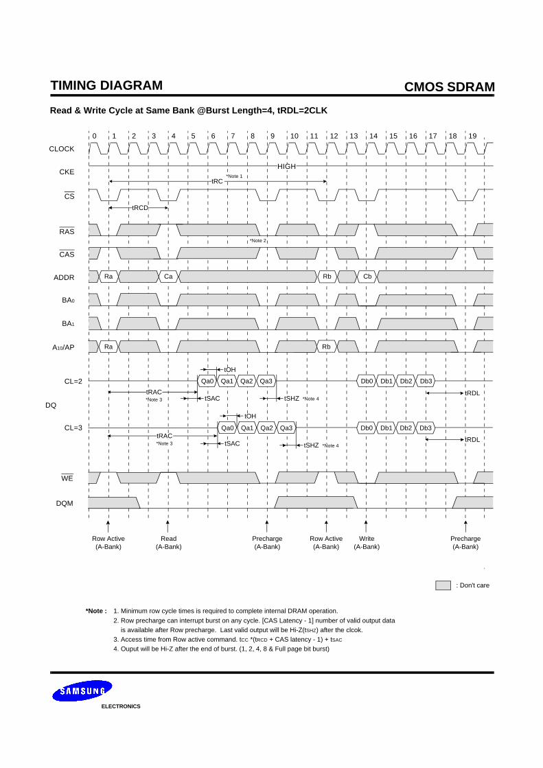
Read & Write Cycle at Same Bank @Burst Length=4, tRDL=2CLK
HIGH
: Don't care
*Note : 1. Minimum row cycle times is required to complete internal DRAM operation.
2. Row precharge can interrupt burst on any cycle. [CAS Latency - 1] number of valid output data is available after Row precharge. Last valid output will be Hi-Z(tSHZ) after the clcok.3. Access time from Row active command. tCC *(tRCD + CAS latency - 1) + tSAC
4. Ouput will be Hi-Z after the end of burst. (1, 2, 4, 8 & Full page bit burst)
*Note 1tRC
tRCD
*Note 2
tRDL
tRDL
tSHZ *Note 4
tSHZ *Note 4
tOH
tRAC*Note 3 tSAC
tSACtRAC*Note 3
tOH
BA0
BA1
A10/AP
CL=2
CL=3
DQ
ADDR
CAS
RAS
CS
CKE
CLOCK
Ra Rb
Qa0 Qa1 Qa2 Qa3
Qa0 Qa1 Qa2 Qa3
Db0 Db1 Db2 Db3
Db0 Db1 Db2 Db3
Ra Ca Rb Cb
WE
DQM
Row Active(A-Bank)
Precharge(A-Bank)
Row Active(A-Bank)
Write(A-Bank)
Precharge(A-Bank)
Read(A-Bank)

TIMING DIAGRAM CMOS SDRAM
ELECTRONICS
0 1 2 3 4 5 6 7 8 9 10 11 12 13 14 15 16 17 18 19
Page Read & Write Cycle at Same Bank @Burst Length=4, tRDL=1CLK
HIGH
Row Active(A-Bank)
Read(A-Bank)
Write(A-Bank)
Precharge(A-Bank)
: Don't care
*Note : 1. To write data before burst read ends, DQM should be asserted three cycle prior to write command to avoid bus contention.2. Row precharge will interrupt writing. Last data input, tRDL before Row precharge, will be written.3. DQM should mask invalid input data on precharge command cycle when asserting precharge before end of burst. Input data after Row precharge cycle will be masked internally. 4. tDAL, last data in to active delay, is 1CLK + 20ns
Read(A-Bank)
tRCD
*Note 2
tRDL
*Note 1 *Note 3
tCDL
Qa0 Qa1 Qb0 Qb1 Qb2
Qa0 Qa1 Qb0 Qb1
Dc0 Dc1 Dd0 Dd1
Dc0 Dc1 Dd0 Dd1
Write(A-Bank)
BA0
BA1
A10/AP
CL=2
CL=3
DQ
ADDR
CAS
RAS
CS
CKE
CLOCK
WE
DQM
Ra Ca Cb Cc Cd
Ra
tDAL *Note 4
Rb
Rb
Row Adiwe(A-Bank)

TIMING DIAGRAM CMOS SDRAM
ELECTRONICS
0 1 2 3 4 5 6 7 8 9 10 11 12 13 14 15 16 17 18 19
Page Read & Write Cycle at Same Bank @Burst Length=4, tRDL=2CLK
HIGH
Row Active(A-Bank)
Read(A-Bank)
Write(A-Bank)
Precharge(A-Bank)
: Don't care
*Note : 1. To write data before burst read ends, DQM should be asserted three cycle prior to write command to avoid bus contention.2. Row precharge will interrupt writing. Last data input, tRDL before Row precharge, will be written.3. DQM should mask invalid input data on precharge command cycle when asserting precharge before end of burst. Input data after Row precharge cycle will be masked internally. 4. tDAL ,last data in to active delay, is 2CLK + 20ns.
Read(A-Bank)
tRCD
*Note 2
tRDL
*Note 1 *Note 3
tCDL
Qa0 Qa1 Qb0 Qb1 Qb2
Qa0 Qa1 Qb0 Qb1
Dc0 Dc1 Dd0 Dd1
Dc0 Dc1 Dd0 Dd1
Write(A-Bank)
BA0
BA1
A10/AP
CL=2
CL=3
DQ
ADDR
CAS
RAS
CS
CKE
CLOCK
WE
DQM
Ra Ca Cb Cc Cd
Ra
tDAL *Note 4
Row Active(A-Bank)
Rb
Rb

TIMING DIAGRAM CMOS SDRAM
ELECTRONICS
0 1 2 3 4 5 6 7 8 9 10 11 12 13 14 15 16 17 18 19
Page Read Cycle at Different Bank @Burst Length=4
HIGH
Row Active(A-Bank)
Read(A-Bank)
Read(C-Bank)
Precharge(B-Bank)
Read(D-Bank)
: Don't care
*Note : 1. CS can be don't cared when RAS, CAS and WE are high at the clock high going dege.2. To interrupt a burst read by row precharge, both the read and the precharge banks must be the same.
Row Active(B-Bank)
*Note 2
*Note 1
Row Acive(C-Bank)
Read(B-Bank)
Precharge(A-Bank)
Row Active(D-Bank)
Precharge(C-Bank)
Precharge(D-Bank)
BA0
BA1
A10/AP
CL=2
CL=3
DQ
ADDR
CAS
RAS
CS
CKE
CLOCK
WE
DQM
QAa0 QAa1 QAa2 QBb0 QBb1 QBb2 QCc0 QCc1 QCc2 QDd0 QDd1 QDd2
QAa0 QAa1 QAa2 QBb0 QBb1 QBb2 QCc0 QCc1 QCc2 QDd0 QDd1 QDd2
RAa RBb RCc RDd
RAa RBb CAa RCc CBb RDd CCc CDd

TIMING DIAGRAM CMOS SDRAM
ELECTRONICS
0 1 2 3 4 5 6 7 8 9 10 11 12 13 14 15 16 17 18 19
Page Write Cycle at Different Bank @Burst Length=4, tRDL=1CLK
HIGH
Row Active(A-Bank)
Write(A-Bank)
Row Active(D-Bank)
Write(D-Bank)
: Don't care
*Note : 1. To interrupt burst write by Row precharge, DQM should be asserted to mask invalid input data.2. To interrupt burst write by Row precharge, both the write and the precharge banks must be the same.
Row Active(B-Bank)
tRDL
Row Active(C-Bank)
Precharge(All Banks)
tCDL
Write(B-Bank)
Write(C-Bank)
*Note 1
BA0
BA1
DQ
ADDR
CAS
RAS
CS
CKE
CLOCK
WE
DQM
A10/AP
RAa RBb CAa CBb RCc RDd CCc CDd
RCc RDdRAa RBb
*Note 2
DAa0 DAa1 DAa2 DAa3 DBb0 DBb1 DBb2 DBb3 DCc0 DCc1 DDd0 DDd1 DDd2

TIMING DIAGRAM CMOS SDRAM
ELECTRONICS
0 1 2 3 4 5 6 7 8 9 10 11 12 13 14 15 16 17 18 19
Page Write Cycle at Different Bank @Burst Length=4, tRDL=2CLK
HIGH
Row Active(A-Bank)
Write(A-Bank)
Row Active(D-Bank)
Write(D-Bank)
: Don't care
*Note : 1. To interrupt burst write by Row precharge, DQM should be asserted to mask invalid input data.2. To interrupt burst write by Row precharge, both the write and the precharge banks must be the same.
Row Active(B-Bank)
tRDL
Row Active(C-Bank)
Precharge(All Banks)
tCDL
Write(B-Bank)
Write(C-Bank)
*Note 1
BA0
BA1
DQ
ADDR
CAS
RAS
CS
CKE
CLOCK
WE
DQM
A10/AP
RAa RBb CAa CBb RCc RDd CCc CDd
RCc RDdRAa RBb
DAa0 DAa1 DAa2 DAa3 DBb0 DBb1 DBb2 DBb3 DCc0 DCc1 DDd0 DDd1 DDd2
*Note 2

TIMING DIAGRAM CMOS SDRAM
ELECTRONICS
0 1 2 3 4 5 6 7 8 9 10 11 12 13 14 15 16 17 18 19
Read & Write Cycle at Different Bank @Burst Length=4
HIGH
RAa
Row Active(A-Bank)
Write(D-Bank)
Row Active(B-Bank)
: Don't care
*Note : 1. tCDL should be met to complete write.
Read(A-Bank)
RAa
CDb RBc
*Note 1tCDL
RDbCAa
RBc
Row Active(D-Bank)
Precharge(A-Bank)
Read(B-Bank)
CBc
RDb
BA0
BA1
A10/AP
CL=2
CL=3
DQ
ADDR
CAS
RAS
CS
CKE
CLOCK
WE
DQM
QAa0 QAa1 QAa2 QAa3
QAa0 QAa1 QAa2 QAa3
DDb0 DDb1 DDb2 DDb3
DDb0 DDb1 DDb2 DDb3
QBc0 QBc1 QBc2
QBc0 QBc1

TIMING DIAGRAM CMOS SDRAM
ELECTRONICS
0 1 2 3 4 5 6 7 8 9 10 11 12 13 14 15 16 17 18 19
Read & Write Cycle with Auto Precharge I @Burst Length=4
HIGH
Row Active(A-Bank)
: Don't care
*Note1: When Read(Write) command with auto precharge is issued at A-Bank after A and B Bank activation. - if Read(Write) command without auto precharge is issued at B-Bank before A-Bank auto precharge starts, A-Bank auto precharge will start at B-Bank read command input point . - any command can not be issued at A-Bank during tRP after A-Bank auto precharge starts.
Row Active(B-Bank)
Read withAuto Precharge
(A-Bank)
Write with Auto Precharge
(A-Bank)
Row Active(A-Bank)
BA0
A10/AP
CL=2
CL=3
DQ
ADDR
CAS
RAS
CS
CKE
CLOCK
WE
DQM
QAa0 QAa1 QBb0 QBb1
QAa0 QAa1 QBb0 QBb1
RAa RBb CAa
RAa RBb
RAcCBb
QBb2 QBb3
Read without Auto precharge(B-Bank)
Auto PrechargeStart Point
(A-Bank)*Note1
Precharge(B-Bank)
DAc0 DAc1
DAc0 DAc1QBb2 QBb3
CAc
RAc
BA1

TIMING DIAGRAM CMOS SDRAM
ELECTRONICS
0 1 2 3 4 5 6 7 8 9 10 11 12 13 14 15 16 17 18 19
Read & Write Cycle with Auto Precharge II @Burst Length=4
HIGH
Row Active(A-Bank)
: Don't care*Note 1: Any command to A-bank is not allowed in this period.
tRP is determined from at auto precharge start point
Read withAuto Precharge
(A-Bank)
Auto PrechargeStart Point(A-Bank)
Row Active(B-Bank)
Read withAuto Precharge
(B-Bank)
BA0
A10/AP
CL=2
CL=3
DQ
ADDR
CAS
RAS
CS
CKE
CLOCK
WE
DQM
Qa0 Qa1 Qa2 Qa3
Qa0 Qa1 Qa2 Qa3
Qb0 Qb1 Qb2 Qb3
Qb0 Qb1 Qb2 Qb3
Ra Ca
Ra
CbRb
Rb
*Note1
Auto PrechargeStart Point(B-Bank)
BA1

TIMING DIAGRAM CMOS SDRAM
ELECTRONICS
0 1 2 3 4 5 6 7 8 9 10 11 12 13 14 15 16 17 18 19
Clock Suspension & DQM Operation Cycle @CAS Latency=2, Burst Length=4
Ra
Row Active ClockSuspension
Read WriteDQM
: Don't care
ClockSuspension
Read
*Note 1
tSHZ tSHZ
WriteDQM
Write
Read DQM
*Note1 : DQM is needed to prevent bus contention.
BA0
BA1
DQ
ADDR
CAS
RAS
CS
CKE
CLOCK
WE
DQM
A10/AP
Ra Ca Cb Cc
Dc2Dc0Qb1Qb0Qa3Qa2Qa1Qa0

TIMING DIAGRAM CMOS SDRAM
ELECTRONICS
0 1 2 3 4 5 6 7 8 9 10 11 12 13 14 15 16 17 18 19
Read Interrupted by Precharge Command & Read Burst Stop Cycle @ Full Page Burst
HIGH
Row Active(A-Bank)
: Don't care
*Note : 1. At full page mode, burst is finished by burst stop or precharge.
2. About the valid DQs after burst stop, it is same as the case of RAS interrupt. Both cases are illustrated above timing diagram. See the label 1, 2 on them. But at burst write, Burst stop and RAS interrupt should be compared carefully. Refer the timing diagram of "Full page write burst stop cycle".3. Burst stop is valid at every burst length.
Precharge (A-Bank)
Burst StopRead(A-Bank)
Read(A-Bank)
1
2
1
2
BA0
BA1
A10/AP
CL=2
CL=3
DQ
ADDR
CAS
RAS
CS
CKE
CLOCK
WE
DQM
QAa0 QAa1 QAa2 QAa3 QAa4
QAa0 QAa1 QAa2 QAa3 QAa4
QAb0 QAb1 QAb2 QAb3 QAb4 QAb5
QAb0 QAb1 QAb2 QAb3 QAb4 QAb5
RAa CAa CAb
RAa

TIMING DIAGRAM CMOS SDRAM
ELECTRONICS
0 1 2 3 4 5 6 7 8 9 10 11 12 13 14 15 16 17 18 19
Write Interrupted by Precharge Command & Write Burst Stop Cycle @ Full Page Burst, tRDL=1CLK
Row Active(A-Bank)
Burst Stop Write(A-Bank)
Precharge(A-Bank)
: Don't care
Write(A-Bank)
*Note 1,2tBDL
*Note : 1. At full page mode, burst is finished by burst stop or precharge.2. Data-in at the cycle of interrupted by precharge can not be written into the corresponding memory cell. It is defined by AC parameter of tRDL.
DQM at write interrupted by precharge command is needed to prevent invalid write.
DQM should mask invalid input data on precharge command cycle when asserting precharge before end of burst. Input data after Row precharge cycle will be masked internally.3. Burst stop is valid at every burst length.
HIGH
tRDL
BA0
BA1
DQ
ADDR
CAS
RAS
CS
CKE
CLOCK
WE
DQM
A10/AP
DAa0 DAa1 DAa2 DAa3 DAa4 DAb0 DAb1 DAb2 DAb3 DAb4 DAb5
RAa CAa CAb
RAa
*Note 1

TIMING DIAGRAM CMOS SDRAM
ELECTRONICS
0 1 2 3 4 5 6 7 8 9 10 11 12 13 14 15 16 17 18 19
Write Interrupted by Precharge Command & Write Burst Stop Cycle @ Full Page Burst, tRDL=2CLK
Row Active(A-Bank)
Burst Stop Write(A-Bank)
Precharge(A-Bank)
: Don't care
Write(A-Bank)
tBDL
*Note : 1. At full page mode, burst is finished by burst stop or precharge.2. Data-in at the cycle of interrupted by precharge can not be written into the corresponding memory cell. It is defined by AC parameter of tRDL.
DQM at write interrupted by precharge command is needed to prevent invalid write.
DQM should mask invalid input data on precharge command cycle when asserting precharge before end of burst. Input data after Row precharge cycle will be masked internally.3. Burst stop is valid at every burst length.
HIGH
tRDL
BA0
BA1
DQ
ADDR
CAS
RAS
CS
CKE
CLOCK
WE
DQM
A10/AP
DAa0 DAa1 DAa2 DAa3 DAa4 DAb0 DAb1 DAb2 DAb3 DAb4 DAb5
RAa CAa CAb
RAa
*Note 1,2*Note 1
TIMING DIAGRAM CMOS SDRAM
ELECTRONICS
0 1 2 3 4 5 6 7 8 9 10 11 12 13 14 15 16 17 18 19
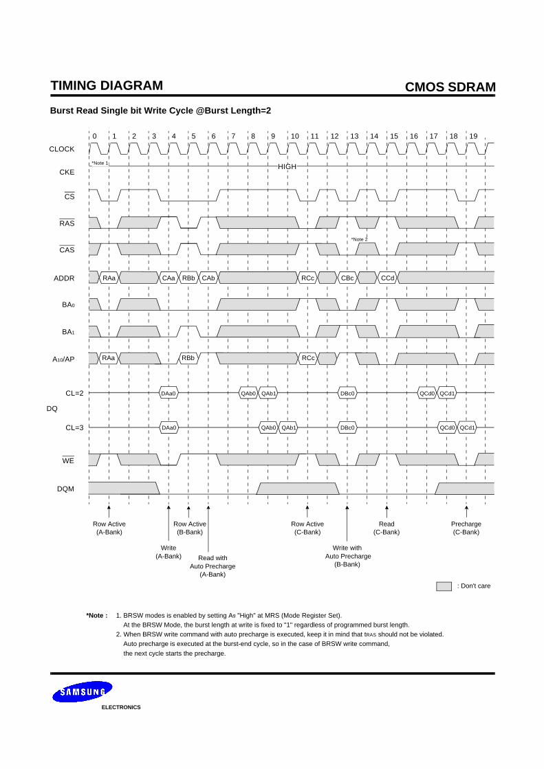
Burst Read Single bit Write Cycle @Burst Length=2
HIGH
Row Active(A-Bank)
Row Active(C-Bank)
Write with Auto Precharge
(B-Bank)
: Don't care
*Note : 1. BRSW modes is enabled by setting A9 "High" at MRS (Mode Register Set). At the BRSW Mode, the burst length at write is fixed to "1" regardless of programmed burst length.2. When BRSW write command with auto precharge is executed, keep it in mind that tRAS should not be violated. Auto precharge is executed at the burst-end cycle, so in the case of BRSW write command,
the next cycle starts the precharge.
Write(A-Bank)
*Note 1
Row Active(B-Bank)
Read(C-Bank)
Read with Auto Precharge
(A-Bank)
Precharge(C-Bank)
*Note 2
BA0
BA1
A10/AP
CL=2
CL=3
DQ
ADDR
CAS
RAS
CS
CKE
CLOCK
WE
DQM
DAa0
DAa0
QAb0 QAb1
QAb0 QAb1 DBc0
DBc0 QCd0 QCd1
QCd0 QCd1
RAa CAa RBb CAb RCc CBc CCd
RCcRAa RBb

TIMING DIAGRAM CMOS SDRAM
ELECTRONICS
0 1 2 3 4 5 6 7 8 9 10 11 12 13 14 15 16 17 18 19
Active/Precharge Power Down Mode @CAS Latency=2, Burst Length=4
Precharge Power-down
Entry
: Don’t Care
*Note : 1. Both banks should be in idle state prior to entering precharge power down mode.
2. CKE should be set high at least 1CLK + tss prior to Row active command.
3. Can not violate minimum refresh specification. (64ms)
*Note 1
Precharge
tSS*Note 2
BA
DQ
ADDR
CAS
RAS
CS
CKE
CLOCK
WE
DQM
A10/AP
tSStSS
Ra Ca
Ra
Qa0 Qa1 Qa2
Row Active
Precharge Power-down
Exit
Active Power-down
Entry
Active Power-down
Exit
Read
tSHZ
*Note 3
*Note 2
~~~~
~~~~
~~~~
~~~~
~~~~
~~~~
~~~~
~~~~
~~~~
~~
~~~~
~~~~
~~~~
~~~~
~~~~
~~~~
~~~~
~~~~
~~~~
~~~~

TIMING DIAGRAM CMOS SDRAM
ELECTRONICS
0 1 2 3 4 5 6 7 8 9 10 11 12 13 14 15 16 17 18 19
Self Refresh Entry & Exit Cycle
Self Refresh Entry
: Don't care
*Note : TO ENTER SELF REFRESH MODE
1. CS, RAS & CAS with CKE should be low at the same clcok cycle.2. After 1 clock cycle, all the inputs including the system clock can be don't care except for CKE.3. The device remains in self refresh mode as long as CKE stays "Low". cf.) Once the device enters self refresh mode, minimum tRAS is required before exit from self refresh.
TO EXIT SELF REFRESH MODE
4. System clock restart and be stable before returning CKE high.5. CS starts from high.6. Minimum tRC is required after CKE going high to complete self refresh exit.7. 4K cycle(64Mb ,128Mb) or 8K cycle(256Mb) of burst auto refresh is required before self refresh entry and after self refresh exit if the system uses burst refresh.
*Note 1
*Note 7
Hi-Z Hi-Z
Self Refresh Exit Auto Refresh
tSS
*Note 2
*Note 3
*Note 4tRCmin
*Note 6
*Note 5
BA0~BA1
DQ
ADDR
CAS
RAS
CS
CKE
CLOCK
WE
DQM
A10/AP
~~~~
~~~~
~~~~
~~~~
~~~~
~~~~
~~~~
~~~~
~~~~
~~
~~~~
~~~~
~~~~
~~~~
~~~~
~~~~
~~~~
~~~~
~~~~ ~~

TIMING DIAGRAM CMOS SDRAM
ELECTRONICS
0 1 2 3 4 5 6 7 8 9 10 11 12 13 14 15 16 17 18 19
Mode Register Set Cycle
HIGH
MRS Auto Refresh
: Don't care
*Note : 1. CS, RAS, CAS, & WE activation at the same clock cycle with address key will set internal mode register.2. Minimum 2 clock cycles should be met before new RAS activation.3. Please refer to Mode Register Set table.
NewCommand
New Command
Hi-Z Hi-Z
tRC
HIGH
MODE REGISTER SET CYCLE
* All banks precharge should be completed before Mode Register Set cycle and auto refresh cycle.
Auto Refresh Cycle
DQ
ADDR
CAS
RAS
CS
CKE
CLOCK
WE
DQM
Key Ra
*Note 3
*Note 1
*Note 2
~~~~
~~~~
~~~~
~~~~
~~~~
~~~~
~~
0 1 2 3 4 5 6 7 8 9 10