Embed Size (px)
DESCRIPTION
xc
Citation preview
Hallmark Circuits, Inc.
“A Commitment To Quality, A Commitment To You”ISO 9002 Certified
Controlled ImpedanceControlled Impedance
from the fabricators viewfrom the fabricators view
Rick NorfolkRick Norfolk
Hallmark Circuits, Inc.
“A Commitment To Quality, A Commitment To You”ISO 9002 Certified
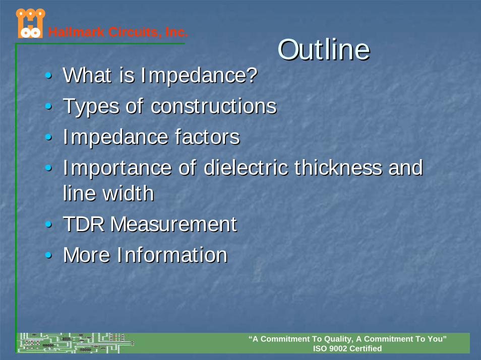
OutlineOutline•• What is Impedance?What is Impedance?•• Types of constructionsTypes of constructions•• Impedance factorsImpedance factors•• Importance of dielectric thickness and Importance of dielectric thickness and
line widthline width•• TDR MeasurementTDR Measurement•• More InformationMore Information
Hallmark Circuits, Inc.
“A Commitment To Quality, A Commitment To You”ISO 9002 Certified
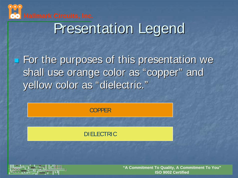
Presentation LegendPresentation Legend
For the purposes of this presentation we For the purposes of this presentation we shall use orange color as “copper” and shall use orange color as “copper” and yellow color as “dielectric.”yellow color as “dielectric.”
COPPER
DIELECTRIC
Hallmark Circuits, Inc.
“A Commitment To Quality, A Commitment To You”ISO 9002 Certified
What is Characteristic What is Characteristic Impedance?Impedance?
•• Definition of terms Definition of terms -- IPC D 317 Design IPC D 317 Design GuidelinesGuidelines
•• Characteristic impedance Characteristic impedance -- The resistance in The resistance in parallel circuits and power planes to the flow of parallel circuits and power planes to the flow of alternating current.alternating current.
•• Measured in ohms as in direct current but this is Measured in ohms as in direct current but this is an alternating current field effect.an alternating current field effect.
Hallmark Circuits, Inc.
“A Commitment To Quality, A Commitment To You”ISO 9002 Certified
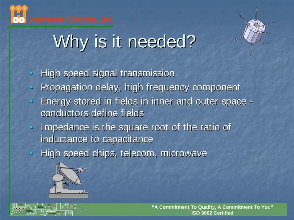
Why is it needed?Why is it needed?
•• High speed signal transmissionHigh speed signal transmission•• Propagation delay, high frequency componentPropagation delay, high frequency component•• Energy stored in fields in inner and outer space Energy stored in fields in inner and outer space --
conductors define fieldsconductors define fields•• Impedance is the square root of the ratio of Impedance is the square root of the ratio of
inductance to capacitanceinductance to capacitance•• High speed chips, telecom, microwaveHigh speed chips, telecom, microwave
Hallmark Circuits, Inc.
“A Commitment To Quality, A Commitment To You”ISO 9002 Certified
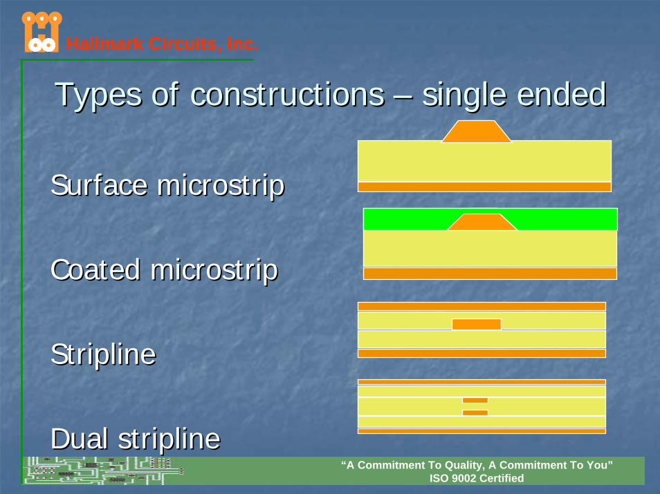
Types of constructions Types of constructions –– single endedsingle ended
Surface Surface microstripmicrostrip
Coated Coated microstripmicrostrip
StriplineStripline
Dual Dual striplinestripline
Hallmark Circuits, Inc.
“A Commitment To Quality, A Commitment To You”ISO 9002 Certified
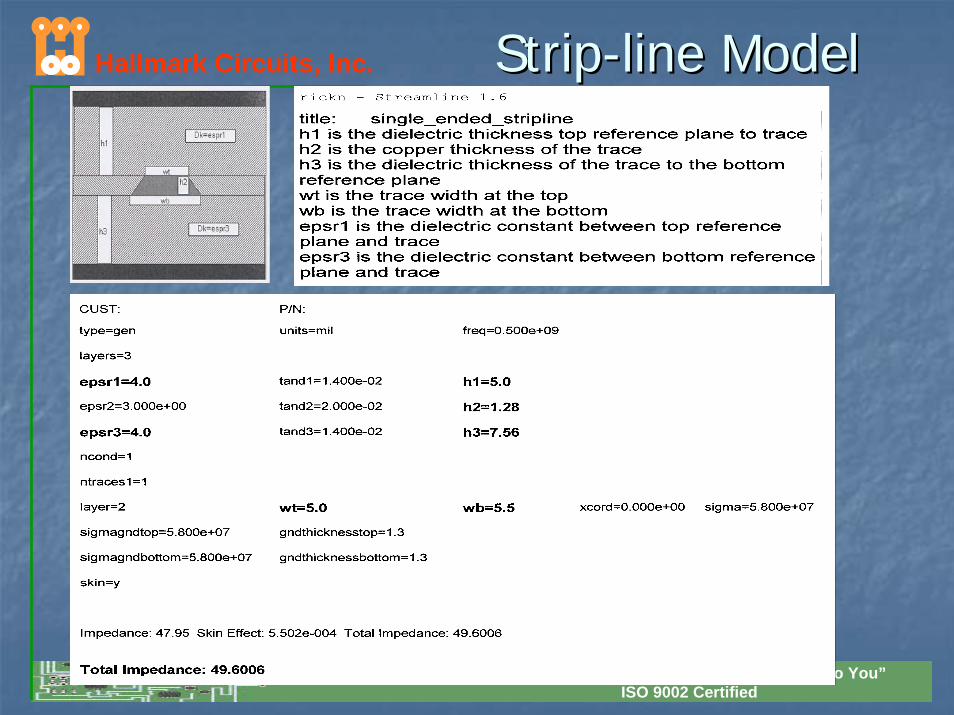
StripStrip--line Modelline Model
Hallmark Circuits, Inc.
“A Commitment To Quality, A Commitment To You”ISO 9002 Certified
Does soldermask affect Does soldermask affect ImpedaneImpedane??“YES IT DOES”“YES IT DOES”
Remember that soldermask, in almost all cases, Remember that soldermask, in almost all cases, will exist over the impedance traces on will exist over the impedance traces on microstripmicrostrip designs. If a drydesigns. If a dry--film mask is used film mask is used this could be anywhere from 3this could be anywhere from 3--4 mils thick and 4 mils thick and could lower the impedance value as much as 7 could lower the impedance value as much as 7 ohms. Typical thickness of an LPI mask over ohms. Typical thickness of an LPI mask over the traces is .5 mil and the impedance value is the traces is .5 mil and the impedance value is only affected typically by 2 ohms. Due to very only affected typically by 2 ohms. Due to very fine lines/spaces these days, dryfine lines/spaces these days, dry--film soldermask film soldermask is rarely used any longer.is rarely used any longer.
Hallmark Circuits, Inc.
“A Commitment To Quality, A Commitment To You”ISO 9002 Certified
ANSWER!ANSWER!
ABSOLUTELY NOTHING!!!!!! (Depending on who you talk ABSOLUTELY NOTHING!!!!!! (Depending on who you talk to!!!!)to!!!!)
Most vendors would need to use a thickness of 4.2 to 4.5 Most vendors would need to use a thickness of 4.2 to 4.5 nominal value to support this requirement. This would nominal value to support this requirement. This would not have that much of an affect except in the case of not have that much of an affect except in the case of micromicro--strip and dualstrip and dual--stripstrip--line configurations. For microline configurations. For micro--strip a line width of approximately 7 mils would be strip a line width of approximately 7 mils would be needed and for dualneeded and for dual--stripstrip--lines 5 mils to support this lines 5 mils to support this dielectric thickness. It also will affect the overall thickness dielectric thickness. It also will affect the overall thickness of the board. There are many boards out there that do of the board. There are many boards out there that do not meet this requirement for one reason or another and not meet this requirement for one reason or another and they work perfectly fine.they work perfectly fine.
Hallmark Circuits, Inc.
“A Commitment To Quality, A Commitment To You”ISO 9002 Certified
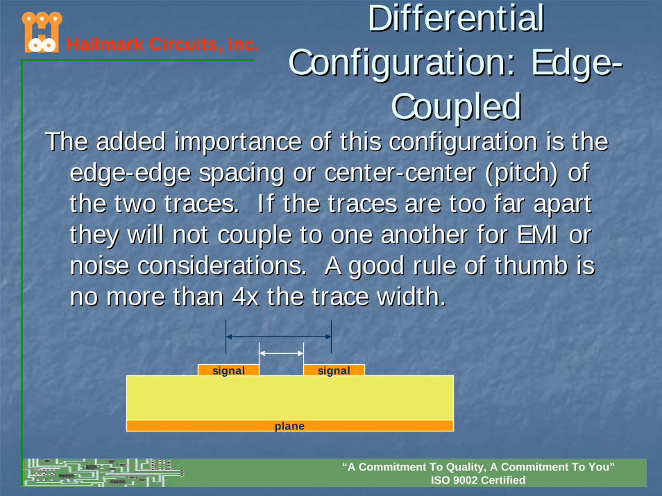
Differential Differential Configuration: EdgeConfiguration: Edge--
CoupledCoupledThe added importance of this configuration is the The added importance of this configuration is the
edgeedge--edge spacing or centeredge spacing or center--center (pitch) of center (pitch) of the two traces. If the traces are too far apart the two traces. If the traces are too far apart they will not couple to one another for EMI or they will not couple to one another for EMI or noise considerations. A good rule of thumb is noise considerations. A good rule of thumb is no more than 4x the trace width.no more than 4x the trace width.
plane
signal signal
Hallmark Circuits, Inc.
“A Commitment To Quality, A Commitment To You”ISO 9002 Certified
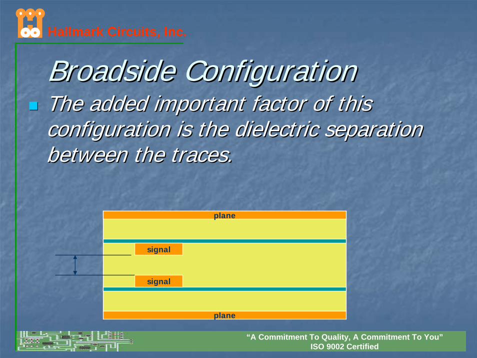
Broadside ConfigurationBroadside ConfigurationThe added important factor of this The added important factor of this configuration is the dielectric separation configuration is the dielectric separation between the traces.between the traces.
plane
plane
signal
signal
Hallmark Circuits, Inc.
“A Commitment To Quality, A Commitment To You”ISO 9002 Certified
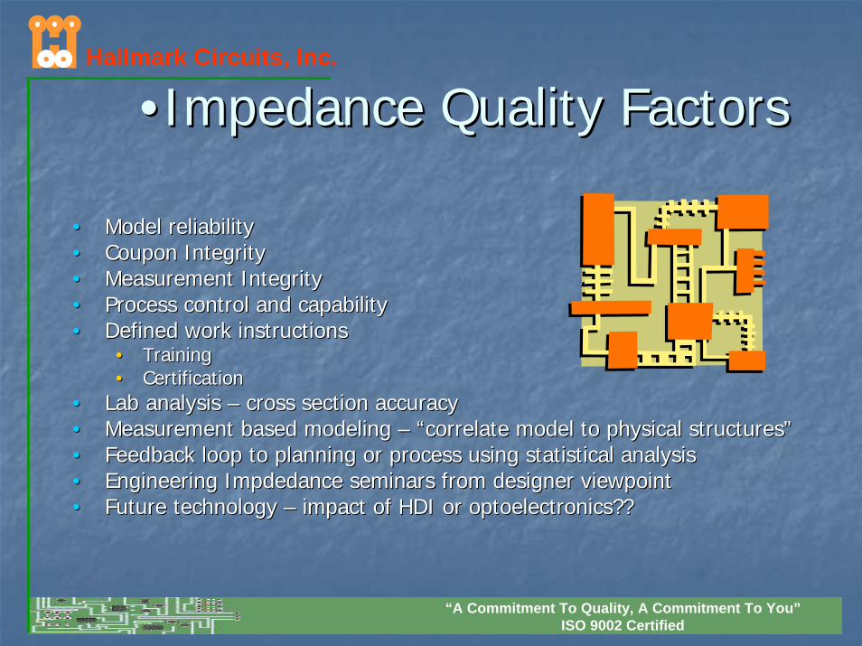
••Impedance Quality FactorsImpedance Quality Factors
•• Model reliabilityModel reliability•• Coupon IntegrityCoupon Integrity•• Measurement IntegrityMeasurement Integrity•• Process control and capabilityProcess control and capability•• Defined work instructionsDefined work instructions
•• TrainingTraining•• CertificationCertification
•• Lab analysis Lab analysis –– cross section accuracycross section accuracy•• Measurement based modeling Measurement based modeling –– “correlate model to physical structures”“correlate model to physical structures”•• Feedback loop to planning or process using statistical analysisFeedback loop to planning or process using statistical analysis•• Engineering Engineering ImpdedanceImpdedance seminars from designer viewpointseminars from designer viewpoint•• Future technology Future technology –– impact of HDI or optoelectronics??impact of HDI or optoelectronics??
Hallmark Circuits, Inc.
“A Commitment To Quality, A Commitment To You”ISO 9002 Certified
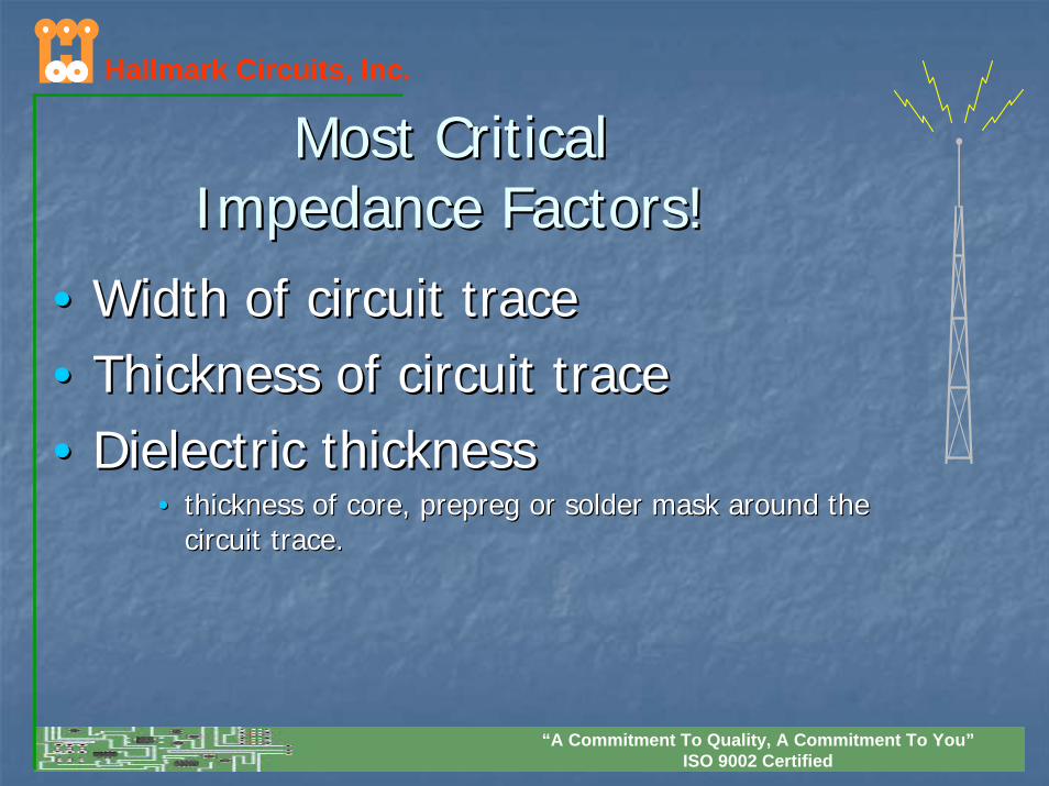
Most Critical Most Critical Impedance Factors!Impedance Factors!
•• Width of circuit traceWidth of circuit trace•• Thickness of circuit traceThickness of circuit trace•• Dielectric thicknessDielectric thickness
•• thickness of core, prepreg or solder mask around the thickness of core, prepreg or solder mask around the circuit trace.circuit trace.
Hallmark Circuits, Inc.
“A Commitment To Quality, A Commitment To You”ISO 9002 Certified
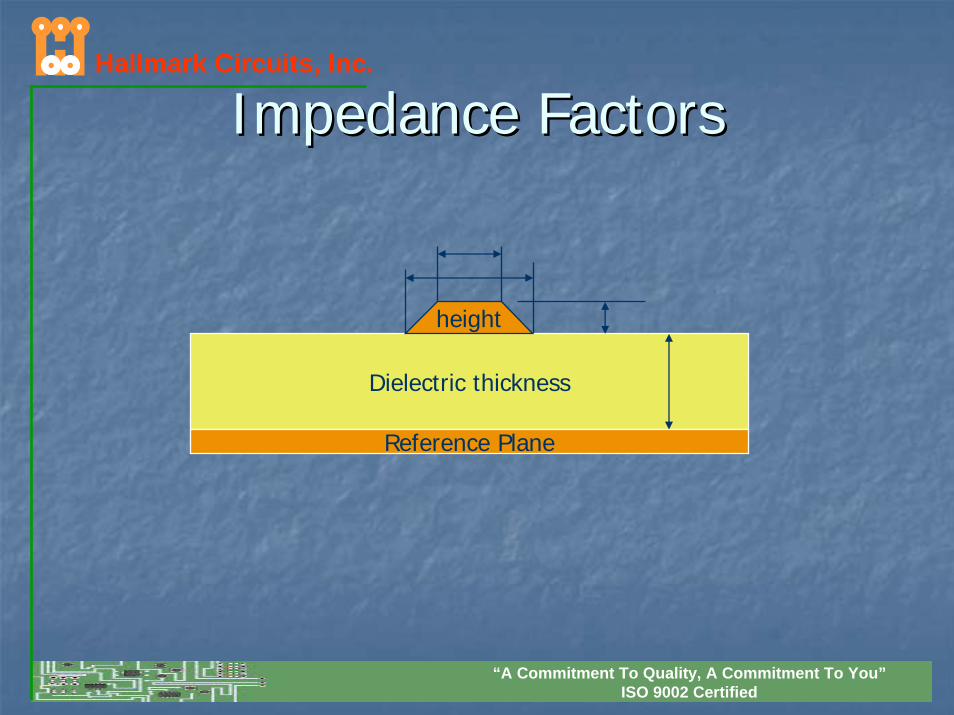
Impedance FactorsImpedance Factors
Dielectric thickness
Reference Plane
height
Hallmark Circuits, Inc.
“A Commitment To Quality, A Commitment To You”ISO 9002 Certified
Additional factors to consider!Additional factors to consider!1.1. DielectricDielectric Constant (Constant (DkDk) of the material being) of the material being usedused..
This is sometimes known as This is sometimes known as ErEr. It is the ability of a material to hold an electromagnetic ch. It is the ability of a material to hold an electromagnetic charge with air or spacearge with air or spaceas 1. This is a function of the materials (resin, gas 1. This is a function of the materials (resin, glass, soldermask, and air) that a circuit passes a signal througlass, soldermask, and air) that a circuit passes a signal through.h.Typical Typical Dk’sDk’s for circuit boards built with FR4 material range from 4.2 to 4.for circuit boards built with FR4 material range from 4.2 to 4.8.8.
2. Skin (AC flow is mostly near the outer surface of a solid 2. Skin (AC flow is mostly near the outer surface of a solid electrical conductor.electrical conductor.
3. Soldermask thickness and it’s 3. Soldermask thickness and it’s DkDk value.value.
4. Trapezoid configuration of the traces.4. Trapezoid configuration of the traces.
Hallmark Circuits, Inc.
“A Commitment To Quality, A Commitment To You”ISO 9002 Certified
Importance of Importance of dielectric thickness and dielectric thickness and
line widthline width
•• Dielectric thickness is a function of core/prepreg Dielectric thickness is a function of core/prepreg selection and lamination parameters.selection and lamination parameters.
•• Line width is a result of plotting, imaging, developing, Line width is a result of plotting, imaging, developing, and etching.and etching.
•• Dielectric thickness and line width are the two most Dielectric thickness and line width are the two most important factors in meeting impedance values.important factors in meeting impedance values.
Hallmark Circuits, Inc.
“A Commitment To Quality, A Commitment To You”ISO 9002 Certified
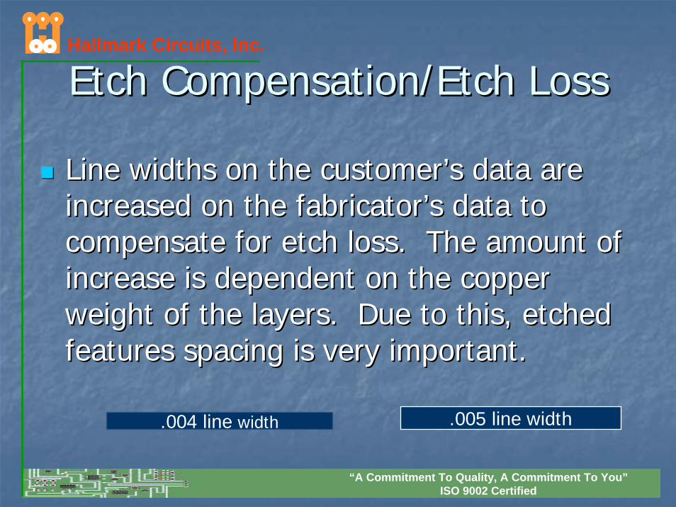
Etch Compensation/Etch LossEtch Compensation/Etch Loss
Line widths on the customer’s data are Line widths on the customer’s data are increased on the fabricator’s data to increased on the fabricator’s data to compensate for etch loss. The amount of compensate for etch loss. The amount of increase is dependent on the copper increase is dependent on the copper weight of the layers. Due to this, etched weight of the layers. Due to this, etched features spacing is very important.features spacing is very important.
.004 line width .005 line width
Hallmark Circuits, Inc.
“A Commitment To Quality, A Commitment To You”ISO 9002 Certified
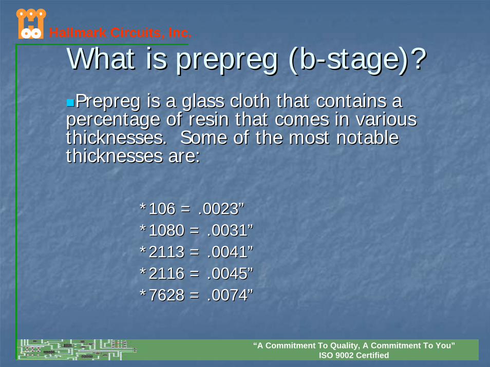
What is prepreg (bWhat is prepreg (b--stage)?stage)?
*106 = .0023”*106 = .0023”*1080 = .0031”*1080 = .0031”*2113 = .0041”*2113 = .0041”*2116 = .0045”*2116 = .0045”*7628 = .0074”*7628 = .0074”
Prepreg is a glass cloth that contains a Prepreg is a glass cloth that contains a percentage of resin that comes in various percentage of resin that comes in various thicknesses. Some of the most notable thicknesses. Some of the most notable thicknesses are:thicknesses are:
Hallmark Circuits, Inc.
“A Commitment To Quality, A Commitment To You”ISO 9002 Certified
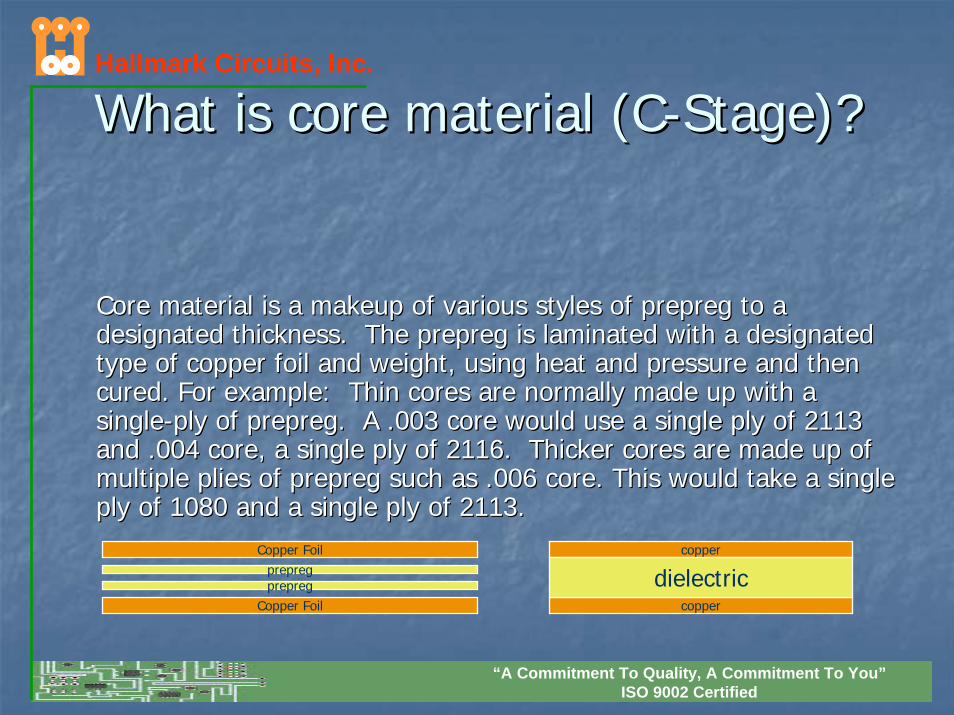
What is core material (CWhat is core material (C--Stage)?Stage)?
Copper Foilprepregprepreg
Copper Foil
copper
copper
dielectric
Core material is a makeup of various styles of prepreg to a Core material is a makeup of various styles of prepreg to a designated thickness. The prepreg is laminated with a designatedesignated thickness. The prepreg is laminated with a designated d type of copper foil and weight, using heat and pressure and thentype of copper foil and weight, using heat and pressure and thencured. For example: Thin cores are normally made up with a cured. For example: Thin cores are normally made up with a singlesingle--ply of prepreg. A .003 core would use a single ply of 2113 ply of prepreg. A .003 core would use a single ply of 2113 and .004 core, a single ply of 2116. Thicker cores are made up and .004 core, a single ply of 2116. Thicker cores are made up of of multiple plies of prepreg such as .006 core. This would take a smultiple plies of prepreg such as .006 core. This would take a single ingle ply of 1080 and a single ply of 2113.ply of 1080 and a single ply of 2113.
Hallmark Circuits, Inc.
“A Commitment To Quality, A Commitment To You”ISO 9002 Certified
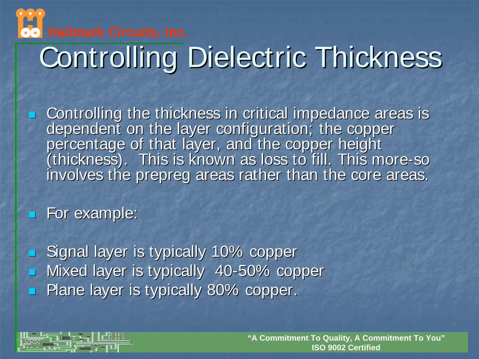
Controlling Dielectric ThicknessControlling Dielectric Thickness
Controlling the thickness in critical impedance areas is Controlling the thickness in critical impedance areas is dependent on the layer configuration; the copper dependent on the layer configuration; the copper percentage of that layer, and the copper height percentage of that layer, and the copper height (thickness). This is known as loss to fill. This more(thickness). This is known as loss to fill. This more--so so involves the prepreg areas rather than the core areas.involves the prepreg areas rather than the core areas.
For example:For example:
Signal layer is typically 10% copperSignal layer is typically 10% copperMixed layer is typically 40Mixed layer is typically 40--50% copper50% copperPlane layer is typically 80% copper.Plane layer is typically 80% copper.
Hallmark Circuits, Inc.
“A Commitment To Quality, A Commitment To You”ISO 9002 Certified
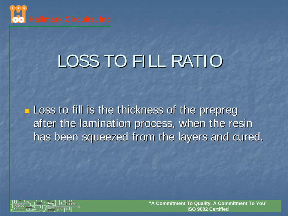
LOSS TO FILL RATIOLOSS TO FILL RATIO
Loss to fill is the thickness of the prepreg Loss to fill is the thickness of the prepreg after the lamination process, when the resin after the lamination process, when the resin has been squeezed from the layers and cured.has been squeezed from the layers and cured.
Hallmark Circuits, Inc.
“A Commitment To Quality, A Commitment To You”ISO 9002 Certified
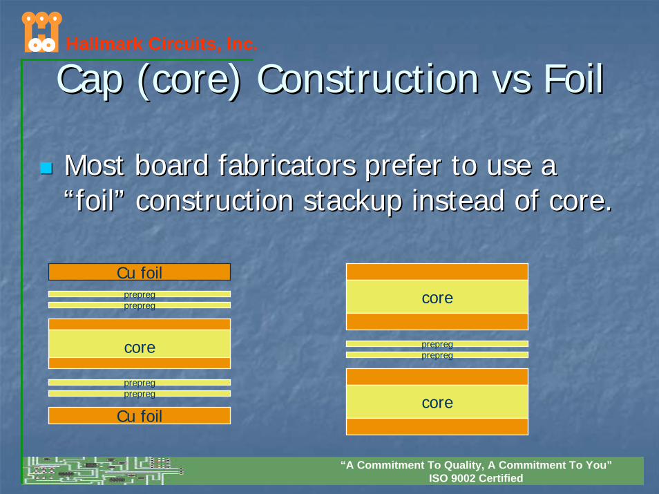
Cap (core) Construction Cap (core) Construction vsvs FoilFoil
Most board fabricators prefer to use a Most board fabricators prefer to use a “foil” construction stackup instead of core.“foil” construction stackup instead of core.
Cu foilprepregprepreg
core
prepregprepreg
Cu foil
core
prepregprepreg
core
Hallmark Circuits, Inc.
“A Commitment To Quality, A Commitment To You”ISO 9002 Certified
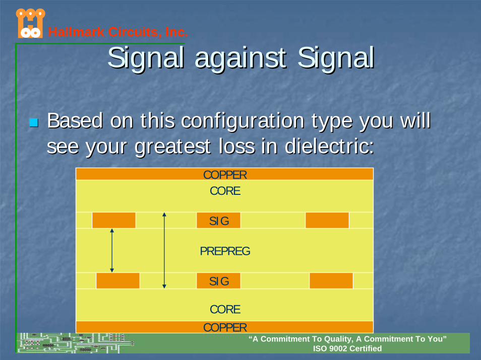
Signal against SignalSignal against Signal
Based on this configuration type you will Based on this configuration type you will see your greatest loss in dielectric:see your greatest loss in dielectric:
CORE
PREPREG
CORE
SIG
SIG
COPPER
COPPER
Hallmark Circuits, Inc.
“A Commitment To Quality, A Commitment To You”ISO 9002 Certified
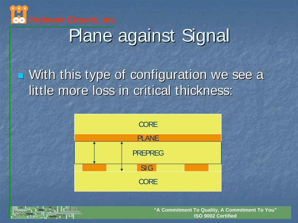
Plane against SignalPlane against Signal
With this type of configuration we see a With this type of configuration we see a little more loss in critical thickness:little more loss in critical thickness:
CORE
CORE
PLANE
SIG
PREPREG
Hallmark Circuits, Inc.
“A Commitment To Quality, A Commitment To You”ISO 9002 Certified
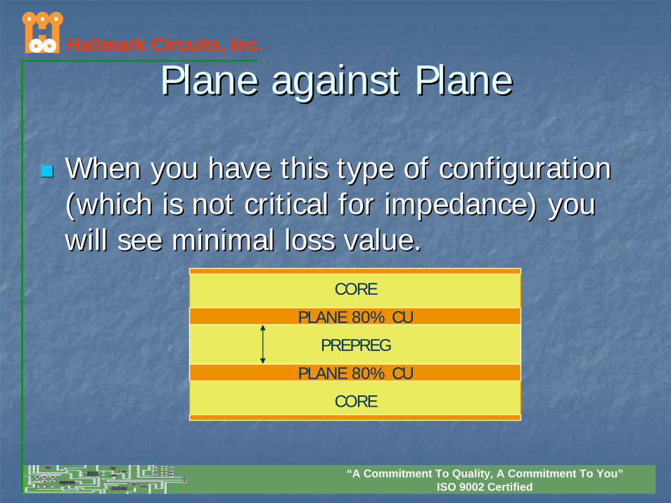
Plane against PlanePlane against Plane
When you have this type of configuration When you have this type of configuration (which is not critical for impedance) you (which is not critical for impedance) you will see minimal loss value.will see minimal loss value.
CORE
CORE
PLANE 80% CU
PLANE 80% CU
PREPREG
Hallmark Circuits, Inc.
“A Commitment To Quality, A Commitment To You”ISO 9002 Certified
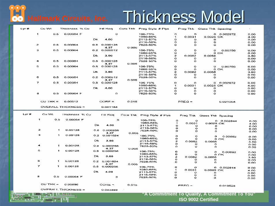
Thickness ModelThickness Model
Hallmark Circuits, Inc.
“A Commitment To Quality, A Commitment To You”ISO 9002 Certified
IPCIPC--6012 MIN. DIELECTRIC6012 MIN. DIELECTRIC
Par 3.6.2.15: “The minimum dielectric spacing shall be Par 3.6.2.15: “The minimum dielectric spacing shall be specified in the procurement documentation (print). If specified in the procurement documentation (print). If the spacing and the number of reinforcing layers are not the spacing and the number of reinforcing layers are not specified, the minimum dielectric spacing is 90um specified, the minimum dielectric spacing is 90um (.0036”) and the number of reinforcing layers may be (.0036”) and the number of reinforcing layers may be selected by the supplier. When the nominal dielectric selected by the supplier. When the nominal dielectric thickness on the drawing is less than 90 um, the thickness on the drawing is less than 90 um, the minimum dielectric spacing is 25 um (.001”) and the minimum dielectric spacing is 25 um (.001”) and the number of reinforcing layers may be selected by the number of reinforcing layers may be selected by the supplier.supplier.
WHAT DOES THIS MEAN?WHAT DOES THIS MEAN?
Hallmark Circuits, Inc.
“A Commitment To Quality, A Commitment To You”ISO 9002 Certified
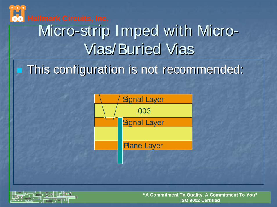
MicroMicro--strip strip ImpedImped with Microwith Micro--Vias/Buried ViasVias/Buried Vias
This configuration is not recommended:This configuration is not recommended:
Signal Layer
Signal Layer
Plane Layer
.003
Hallmark Circuits, Inc.
“A Commitment To Quality, A Commitment To You”ISO 9002 Certified
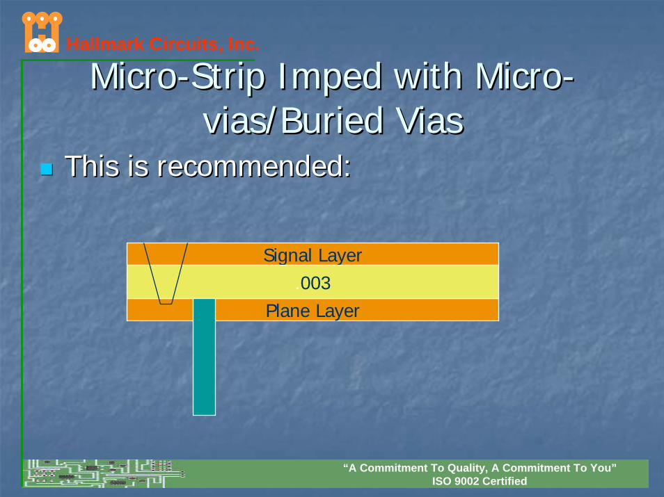
MicroMicro--Strip Strip ImpedImped with Microwith Micro--vias/Buried Viasvias/Buried Vias
This is recommended:This is recommended:
Signal Layer
Plane Layer.003
Hallmark Circuits, Inc.
“A Commitment To Quality, A Commitment To You”ISO 9002 Certified
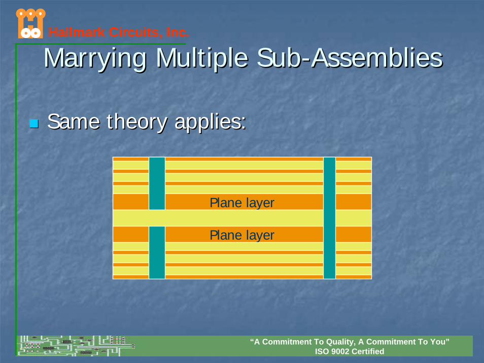
Marrying Multiple SubMarrying Multiple Sub--AssembliesAssemblies
Same theory applies:Same theory applies:
Plane layer
Plane layer
Hallmark Circuits, Inc.
“A Commitment To Quality, A Commitment To You”ISO 9002 Certified
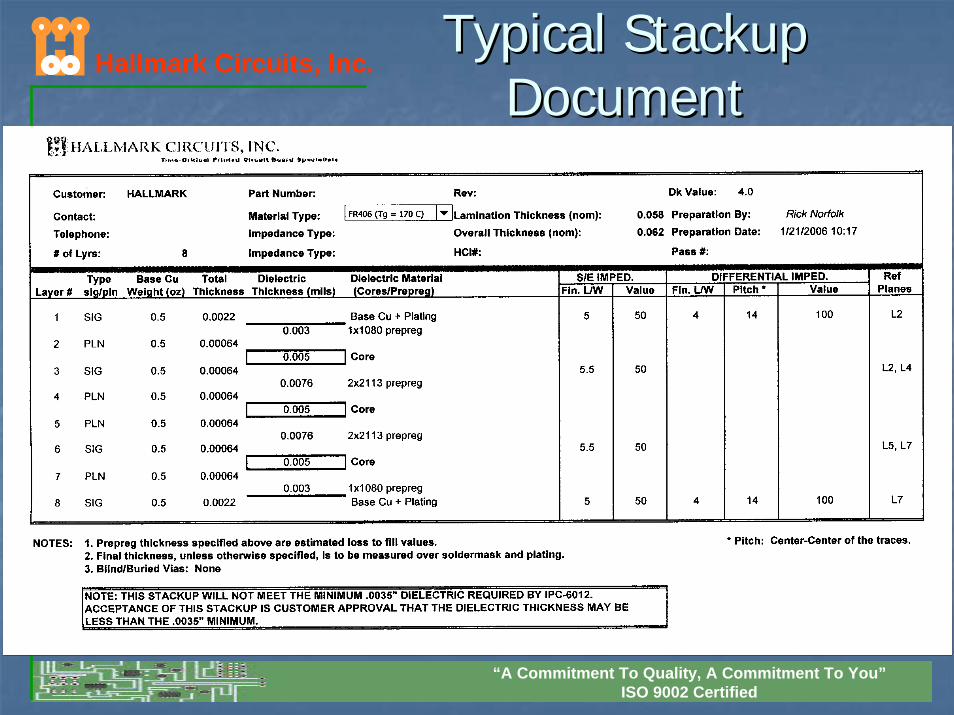
Typical Stackup Typical Stackup DocumentDocument
Hallmark Circuits, Inc.
“A Commitment To Quality, A Commitment To You”ISO 9002 Certified
Mechanical Print NoteMechanical Print Note
* Layers 4,5,8, and 9 using 5 mil line width * Layers 4,5,8, and 9 using 5 mil line width designed to achieve 50 ohm singledesigned to achieve 50 ohm single--ended ended impedance. Layers 1 and 8 using a 5 mil line impedance. Layers 1 and 8 using a 5 mil line width designed to achieve 50 ohm singlewidth designed to achieve 50 ohm single--ended ended impedance and 4 mil line with .012 edgeimpedance and 4 mil line with .012 edge--edge edge spacing (or .016 pitch) to achieve 100 ohm spacing (or .016 pitch) to achieve 100 ohm edgeedge--coupled differential impedance. Vendor coupled differential impedance. Vendor may modify lines/dielectrics as needed to fit may modify lines/dielectrics as needed to fit their processes to achieve required impedance their processes to achieve required impedance values and overall board thickness.values and overall board thickness.
Hallmark Circuits, Inc.
“A Commitment To Quality, A Commitment To You”ISO 9002 Certified
What is Time Domain What is Time Domain ReflectometryReflectometry??
TDR is the analysis of a conductor by sending a TDR is the analysis of a conductor by sending a pulsed signal into the conductor and then pulsed signal into the conductor and then examining the reflection of that pulse.examining the reflection of that pulse.
Hallmark Circuits, Inc.
“A Commitment To Quality, A Commitment To You”ISO 9002 Certified
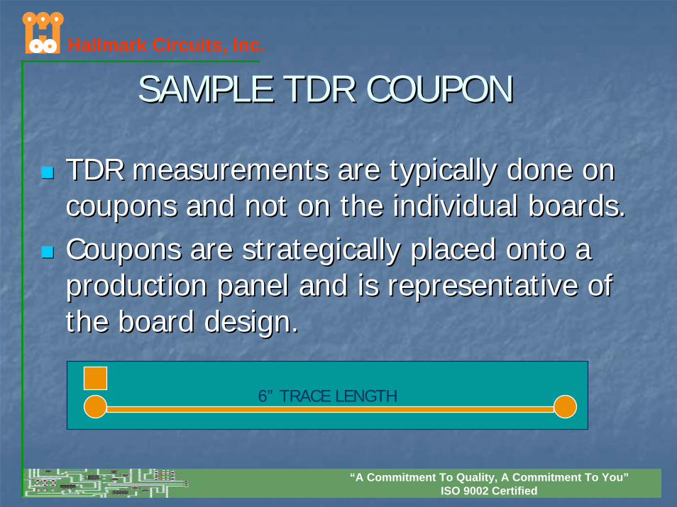
SAMPLE TDR COUPONSAMPLE TDR COUPON
TDR measurements are typically done on TDR measurements are typically done on coupons and not on the individual boards.coupons and not on the individual boards.Coupons are strategically placed onto a Coupons are strategically placed onto a production panel and is representative of production panel and is representative of the board design.the board design.
6” TRACE LENGTH
Hallmark Circuits, Inc.
“A Commitment To Quality, A Commitment To You”ISO 9002 Certified
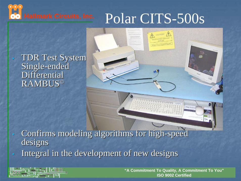
•• TDR Test SystemTDR Test SystemSingleSingle--endedendedDifferentialDifferentialRAMBUSRAMBUS©©
•• Confirms modeling algorithms for highConfirms modeling algorithms for high--speed speed designsdesigns
•• Integral in the development of new designsIntegral in the development of new designs
Polar CITS-500s
Hallmark Circuits, Inc.
“A Commitment To Quality, A Commitment To You”ISO 9002 Certified
RecommendationsRecommendations
If you are declaring that the board is a “designed” impedance, yIf you are declaring that the board is a “designed” impedance, you should specify the ou should specify the finished critical line widths and the dielectric thickness that finished critical line widths and the dielectric thickness that the fabricator is to the fabricator is to maintain. Please keep in mind that the fabricator will not normamaintain. Please keep in mind that the fabricator will not normally do any TDR testing lly do any TDR testing on the board and will maintain your parameters only. The impedaon the board and will maintain your parameters only. The impedance value obtained nce value obtained is the OEM’s responsibility.is the OEM’s responsibility.
Do not handcuff the fabricator. Tell them what impedance value Do not handcuff the fabricator. Tell them what impedance value you are targeting you are targeting with what line widths and leave the rest to them. On your printwith what line widths and leave the rest to them. On your prints, please specify the s, please specify the pitch or edgepitch or edge--edge spacing for diff pairs. Allow them to modify the dielectriedge spacing for diff pairs. Allow them to modify the dielectrics/lines cs/lines as needed for their processes to achieve the required impedance as needed for their processes to achieve the required impedance by placing a note on by placing a note on the fabrication drawing allowing this. Remember, they are the othe fabrication drawing allowing this. Remember, they are the ones responsible for nes responsible for meeting the required impedance.meeting the required impedance.
Work with your vendor as much as possible during the design stagWork with your vendor as much as possible during the design stage to establish a e to establish a viable stackup. Partnership with your vendor during the initial viable stackup. Partnership with your vendor during the initial design phase is very design phase is very important. It’s truly a bummer to find out after all your hard important. It’s truly a bummer to find out after all your hard work that the work that the impedance you are looking for cannot be met with your design criimpedance you are looking for cannot be met with your design criteria.teria.
Hallmark Circuits, Inc.
“A Commitment To Quality, A Commitment To You”ISO 9002 Certified
••Information sourcesInformation sources•• Engineering Solutions, “Controlled Impedance Engineering Solutions, “Controlled Impedance
Workshop”,Bill Workshop”,Bill FujitsuboFujitsubo•• IPC “High Speed Design (IPC IPC “High Speed Design (IPC -- D D -- 317)”317)”•• “High Speed Design Workbook”, Lee Ritchey“High Speed Design Workbook”, Lee Ritchey•• IPC “High Speed, High Frequency Workshop”IPC “High Speed, High Frequency Workshop”


![ASD904 [Rev1-Jan06]](https://img.pdfslide.us/doc/110x75/577cc7fc1a28aba711a1f580/asd904-rev1-jan06.jpg)