Embed Size (px)
Citation preview

Microfl uidics
Screening Conditions for Rationally Engineered Electrodeposition of Nanostructures (SCREEN): Electrodeposition and Applications of Polypyrrole Nanofi bers using Microfl uidic Gradients
Hayden A. Burgoyne , Philseok Kim , * Mathias Kolle , Alexander K. Epstein , and Joanna Aizenberg
A rapid screening method for optimizing electrochemical deposition conditions of polypyrrole (PPy) nanostructures is reported. An electrochemical cell is integrated within a low-cost microfl uidic system, in which electrochemical deposition is carried out across a linear concentration gradient of a reaction parameter. The protocol, refered to as the screening of conditions for rationally engineered electrodeposition of nanostructures (SCREEN), allows rapid screening of conditions for the production of specifi c morphologies by characterizing the electrodeposited samples produced within a chemical gradient. To demonstrate the utility of the SCREEN method, applications in tunable optical coatings and superhydrophobic surfaces are presented.
1. Introduction
The growth of conductive polymers into various nanostruc-
tures has been of great interest in recent years due to the wide
range of applications for which these polymers could be used.
In particular, 1D nanofi bers have been proposed as useful
structures for electrochromic devices, [ 1–3 ] super capacitors, [ 4 , 5 ]
fi eld-effect transistors, [ 6 ] controlled drug-release devices, [ 7 ]
and chemical sensors. [ 8 ] Various approaches using both
soft [ 9–11 ] and hard templates [ 12 ] have been used in the past
© 2012 Wiley-VCH Verlag Gmb
DOI: 10.1002/smll.201200888
H. A. Burgoyne, Dr. P. Kim, Dr. M. Kolle, Dr. A. K. Epstein, Prof. J. AizenbergSchool of Engineering and Applied SciencesHarvard UniversityCambridge, MA 02138, USA E-mail: [email protected]
Dr. P. Kim, Prof. J. Aizenberg Wyss Institute for Biologically Inspired EngineeringHarvard UniversityCambridge, MA 02138, USA
Prof. J. AizenbergDepartment of Chemistry and Chemical BiologyHarvard UniversityCambridge, MA 02138, USA
small 2012, DOI: 10.1002/smll.201200888
to grow nanofi bers, and simple, template-free approaches
have been developed more recently. [ 13–16 ] The ability to
control the formation of polypyrrole (PPy) nanofi bers is
of particular interest due to their high conductivity, envi-
ronmental stability, and biocompatibility. [ 17 ] Furthermore,
Py can be electrochemically polymerized, [ 18–20 ] allowing
for much greater control over the location and duration of
polymerization. However, the morphology, size, and den-
sity of electrodeposited PPy structures are acutely sensitive
to the precise deposition conditions, such as concentration
of monomer, concentration and pH of electrolytes, applied
voltage, and time of deposition; even slight modifi cations of
these conditions can lead to divergent morphologies (fi lms,
fi bers, bowls, cones, etc.). [ 21–23 ] In order to fi nd the optimized
set of electrochemical deposition conditions for the growth
of a desired particular morphology (e.g., nanofi bers), multiple
samples must be prepared from depositions in bulk solutions
by varying a single parameter at a time for each experiment.
Therefore these experiments typically require large volumes
of reagents and substrates, become time-consuming, and gen-
erate a large volume of chemical waste.
Here we report a low-cost, benchtop-based, and green
protocol that we refer to as SCREEN (screening conditions
for rationally engineered electrodeposition of nanostruc-
tures), integrating a microfl uidic gradient generator with an
electrochemical cell to quickly screen a number of chemical
1H & Co. KGaA, Weinheim wileyonlinelibrary.com

H. A. Burgoyne et al.full papers
Figure 1 . A) Schematic of experimental setup. The microfl uidic device creates a gradient of two input liquids. A potential is applied via a potentiostat to the electrodes (WE: working electrode; CE: counter electrode; RE: reference electrode) embedded within the microfl uidic device, where electrochemical polymerization occurs across the chemical gradient. B) CAD image of overhead view of the microfl uidic channels and electrodes on a glass microscope slide.
parameters that govern the morphology
of the resultant electrodeposited PPy on
a substrate. The use of microfl uidic gradi-
ents to perform experiments with a range
of parameters has been previously demon-
strated with applications such as biological
and chemical sensors as well as fabrica-
tion of nanostructured materials. [ 24–26 ]
The method does not require costly and
time-consuming photolithographic proc-
esses to fabricate the microfl uidic devices;
instead it uses inexpensive materials
and rapid fabrication techniques such as
Kapton tape and laser cutting. Using the
SCREEN procedure, we are able to create
various electrodeposition conditions that
lead to numerous nanoscale morphologies
of electrodeposited PPy, each of which is
potentially suitable for various applica-
tions. The information gathered from the
gradient experiments is verifi ed in bulk
deposition in a conventional electro-
chemical cell over a large area. Given the
broad range of their potential applications,
PPy nanofi bers are investigated in more
detail, and we demonstrate quickly opti-
2
mized deposition conditions that result in fi brous surfaces
with controlled optical and wetting characteristics. We envi-
sion that our method can serve as a toolkit for optimizing
the electrochemical deposition processes for many other
materials, such as minerals, inorganics, hydrogels, or hybrid
materials. SCREEN will enable better understanding of the
nucleation and growth behavior and facilitate solution-based
directed electrochemical synthesis and assembly of novel
nanomaterials.
2. Results and Discussion
2.1. Screening of Deposition Conditions
A schematic of the experimental setup is shown in Figure 1 .
The microfl uidic device creates a concentration gradient of
the two input liquids through a series of branching, recom-
bining, and mixing channels under laminar fl ow until a gra-
dient with a suitable number of intermediate concentrations
is reached. The gradient is then merged into a single channel,
which guides the graded reagent solution over the electrodes
where the electrodeposition is induced. The device is fabri-
cated by fi rst using a commercial laser cutter to create the
gradient generator pattern in Kapton tape attached to a glass
slide. Polydimethylsiloxane (PDMS) is cast on this master
pattern to prepare a microfl uidic gradient generator, which
is then bonded to a glass slide with patterned electrodes
for electrodeposition. A potential is applied via a poten-
tiostat to the three electrodes in the microfl uidic channel,
and following electrochemical polymerization across the
www.small-journal.com © 2012 Wiley-VCH V
chemical gradient, the resultant continuum of morphologies
is observed. The concentration profi le is confi rmed to be
linear by measuring the fl uorescence intensity gradient of
Rhodamine dye under UV light, as previously described. [ 27 ]
Furthermore, the electrodes are made to be thin relative to
the length of the channel so that the gradient can be uti-
lized before diffusion smoothes the gradient profi le and so
that the concentration of reactants consumed during elec-
trodeposition does not signifi cantly change over the width
of the electrode. Therefore, an ideal linear concentration
gradient, constant across the entire width of the electrode, is
assumed when caluculating concentration corresponding to
a specifi c location in the gradient.
The deposition conditions for growing 1D polypyrrole
nanofi bers without using a template have been previously
investigated, [ 13 , 14 ] but our method provides fast access to a
large range of parameters and high resolution in the para-
meter space, enabling rapid discovery of ideal deposition con-
ditions. Using previously identifi ed conditions as a baseline
about which the gradients could be set, the following chem-
ical parameters are explored: the concentration of the pyrrole
(Py) monomer, the concentration of the phosphate buffered
saline (PBS), and the pH of the PBS. After deposition, the
morphologies arising from a large set of electrochemical
parameters are observed, and the conditions for most consist-
ently growing 1D PPy nanofi bers can be determined.
2.1.1. Screening for the Optimal Monomer Concentration
A concentration gradient of Py monomer from 0 to 0.15 m in
0.25 m PBS (pH 6.8) and 0.07 m lithium perchlorate (LiClO 4 )
was established across the electrodeposition zone. A potential
of 0.85 V versus the gold pseudo-reference electrode was con-
stantly applied for 10 min. The scanning electron microscopy
erlag GmbH & Co. KGaA, Weinheim small 2012, DOI: 10.1002/smll.201200888

SCREEN: Electrodeposition of Polypyrrole Nanofi bers using Microfl uidics
Figure 2 . SEM images of different regions of a single sample grown under a gradient of Py concentration with concentrations of A) 0.014, B) 0.027, C) 0.041, D) 0.055, E) 0.068, F) 0.082, G) 0.095, H) 0.109, I) 0.123, and J) 0.136 M with 0.07 M LiClO 4 and 0.25 M PBS (pH 7.5). The scale bar for all images is 800 nm. Images were taken at evenly spaced intervals along the direction of the gradient.
(SEM) images of the morphologies formed on the working
electrode after electrodeposition are shown in Figure 2 . With
very low Py concentration, the growth was predictably sparse
with random nucleation of small amounts. As the concentra-
tion rose, both the rate of nucleation and growth increased,
showing more deposition and the beginning of a preference
for one-dimensionality of the growing polymer. With contin-
ually increasing Py concentration, the rate of new nucleation
(parasitic nucleation) began to overwhelm the growth rate of
unbranched, 1D fi bers and resulted in caulifl ower-like struc-
tures. The most consistent growth of long, thin nanofi bers was
observed near the center of the gradient, corresponding to
a concentration of 0.075 m Py. This concentration was used
for many subsequent experiments to further optimize other
parameters.
2.1.2. Screening for the Optimal pH Range
A gradient of the pH of 0.25 m PBS was established between
5 and 8 while the concentrations for Py and LiClO 4 were
kept constant at 0.075 and 0.07 m , respectively. A potential
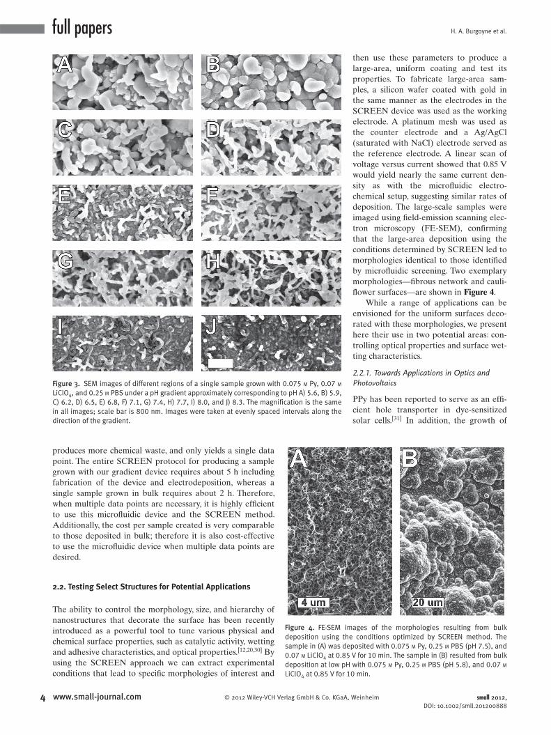
of 0.85 V was constantly applied for 10 min. In Figure 3 , the
© 2012 Wiley-VCH Verlag GmbH & Co. KGaA, Weinhesmall 2012, DOI: 10.1002/smll.201200888
pH had a major effect on the observed
morphologies, as the rate of polymeriza-
tion tends to be higher at lower pH. At a
slightly basic pH, fi brous morphology was
consistently observed. At lower pH, thicker
fi lms of PPy covered the surface with hier-
archical structures of 10–100 μ m mounds
covered with much smaller 100 nm bumps.
The deposition condition we found for this
two-tiered hierarchical structure is remark-
ably useful because it can be created via
a single-step deposition. Furthermore, by
performing a two-step deposition process
in which a second layer is deposited on
top of this hierarchical surface using the
conditions that yield nanofi bers, the sur-
face can be made to display three-tiered
hierarchy. The functions of such a multi-
scale surface topography include extreme
wettability properties, i.e., superhydrophil-
licity or superhydrophobicity, depending
on surface treatment after deposition. [ 28 ]
Furthermore, at the lowest pH, conical
structures begin to form, reminiscent of
conductive polymer structures used for
supercapacitors. [ 29 ]
2.1.3. Screening for the Optimal PBS Concentration
A concentration gradient of PBS was
established in a microfl uidic device from
0.15 to 0.35 m (pH 7.5) while the concen-
trations for Py and LiClO 4 were kept con-
stant at 0.075 and 0.07 m , respectively. A
potential of 0.85 V was constantly applied
for 10 min. The effect of the concentration
of PBS in this range was found to be minimal. PPy deposition
was observed over the entire sample, and changes in mor-
phology were very slight and randomly distributed, as shown
in the Supporting Information (SI), Figure S1. Over multiple
samples, the area corresponding to 0.25 m PBS was observed
to have relatively consistent morphology and was fully cov-
ered with electrodeposited PPy.
Each of these results was verifi ed to be reproducible. Fur-
thermore, given the results of the pH gradient, which showed
that more consistent nanofi bers could be achieved at a higher
pH, the experiment investigating the gradient of the mon-
omer concentration was repeated at different pH values as
well (5.8, 6.8, and 7.5).
Our SCREEN technique of using a microfl uidic gradient
generator to combinatorially determine deposition condi-
tions proved to be extremely effi cient, in both time and cost,
compared to testing individual conditions in bulk solution on
a large sample. A single experiment provided information
with enough resolution to fi nd the ideal conditions for depo-
sition of a desired morphology from a continuum of values
of a chemical parameter being investigated. The bulk deposi-
tion process requires signifi cantly more consumed materials,
3www.small-journal.comim
H. A. Burgoyne et al.
4
full papers
Figure 3 . SEM images of different regions of a single sample grown with 0.075 M Py, 0.07 M LiClO 4 , and 0.25 M PBS under a pH gradient approximately corresponding to pH A) 5.6, B) 5.9, C) 6.2, D) 6.5, E) 6.8, F) 7.1, G) 7.4, H) 7.7, I) 8.0, and J) 8.3. The magnifi cation is the same in all images; scale bar is 800 nm. Images were taken at evenly spaced intervals along the direction of the gradient.
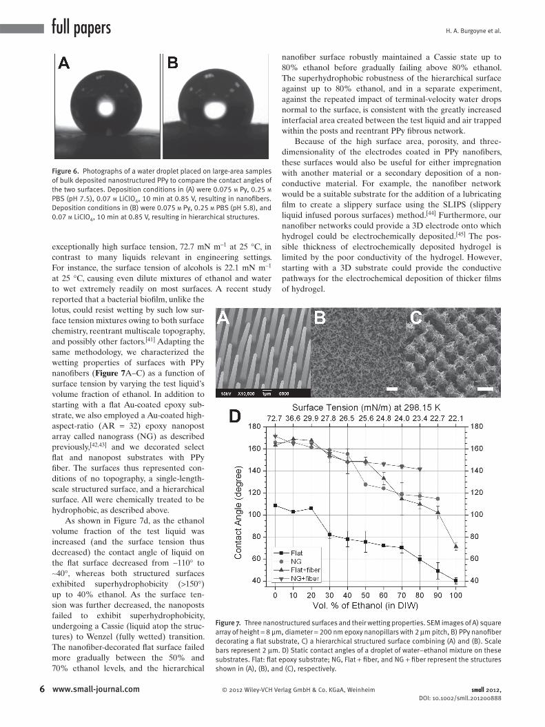
Figure 4 . FE-SEM images of the morphologies resulting from bulk deposition using the conditions optimized by SCREEN method. The sample in (A) was deposited with 0.075 M Py, 0.25 M PBS (pH 7.5), and 0.07 M LiClO 4 at 0.85 V for 10 min. The sample in (B) resulted from bulk deposition at low pH with 0.075 M Py, 0.25 M PBS (pH 5.8), and 0.07 M LiClO 4 at 0.85 V for 10 min.
produces more chemical waste, and only yields a single data
point. The entire SCREEN protocol for producing a sample
grown with our gradient device requires about 5 h including
fabrication of the device and electrodeposition, whereas a
single sample grown in bulk requires about 2 h. Therefore,
when multiple data points are necessary, it is highly effi cient
to use this microfl uidic device and the SCREEN method.
Additionally, the cost per sample created is very comparable
to those deposited in bulk; therefore it is also cost-effective
to use the microfl uidic device when multiple data points are
desired.
2.2. Testing Select Structures for Potential Applications
The ability to control the morphology, size, and hierarchy of
nanostructures that decorate the surface has been recently
introduced as a powerful tool to tune various physical and
chemical surface properties, such as catalytic activity, wetting
and adhesive characteristics, and optical properties. [ 12 , 20 , 30 ] By
using the SCREEN approach we can extract experimental
conditions that lead to specifi c morphologies of interest and
www.small-journal.com © 2012 Wiley-VCH Verlag GmbH & Co. KGa
then use these parameters to produce a
large-area, uniform coating and test its
properties. To fabricate large-area sam-
ples, a silicon wafer coated with gold in
the same manner as the electrodes in the
SCREEN device was used as the working
electrode. A platinum mesh was used as
the counter electrode and a Ag/AgCl
(saturated with NaCl) electrode served as
the reference electrode. A linear scan of
voltage versus current showed that 0.85 V
would yield nearly the same current den-
sity as with the microfl uidic electro-
chemical setup, suggesting similar rates of
deposition. The large-scale samples were
imaged using fi eld-emission scanning elec-
tron microscopy (FE-SEM), confi rming
that the large-area deposition using the
conditions determined by SCREEN led to
morphologies identical to those identifi ed
by microfl uidic screening. Two exemplary
morphologies—fi brous network and cauli-
fl ower surfaces—are shown in Figure 4 .
While a range of applications can be
envisioned for the uniform surfaces deco-
rated with these morphologies, we present
here their use in two potential areas: con-
trolling optical properties and surface wet-
ting characteristics.
2.2.1. Towards Applications in Optics and Photovoltaics
PPy has been reported to serve as an effi -
cient hole transporter in dye-sensitized
solar cells. [ 31 ] In addition, the growth of
A, Weinheim small 2012, DOI: 10.1002/smll.201200888

SCREEN: Electrodeposition of Polypyrrole Nanofi bers using Microfl uidics
hierarchical PPy structures with high surface area and large
scattering and absorption cross-section could be benefi cial
for the development of ultra-black surface coatings similar in
function to the melanin-loaded structures found on the wing
scales of Papilio butterfl ies. [ 32 ] This could be benefi cial for effi -
cient thermal collectors or provision of visual stark contrast
in a variety of active and passive display technologies. Since
PPy exhibits a broad band absorption in the visible range, the
refl ection of the fi lms was characterized across the gradients
in order to observe how the refl ectance varied with the mor-
phology. The intensity of white light refl ected from the PPy on
the gold electrode was measured using a micro-spectroscope
allowing collection of spectra from 20 μ m wide spots on the
sample. After 10 min of deposition, a sample grown under a
gradient of Py monomer showed a dramatic change from the
refl ection of bare gold at low concentrations of Py to effec-
tively zero refl ectance once a fi lm had been deposited. These
measurements are shown in Figure 5 A. The refl ectance of
© 2012 Wiley-VCH Verlag Gmb
Figure 5 . Plots of the refl ectivity of different samples with PPy structures on the gold electrode after 10 min of deposition along each of three gradients. Each data point represents the refl ectivity of a spot of 20 μ m diameter acquired by scanning along the sample in the direction of the gradient under which the sample was deposited. Sample (A) was deposited with a Py concentration gradient, (B) was deposited with a pH gradient, and (C) was deposited with a gradient of PBS concentration.
small 2012, DOI: 10.1002/smll.201200888
PPy samples across pH and PBS concentration gradients was
also measured and is shown in Figure 5 B and C, respectively.
In electrochromic applications of conductive polymers, such
as windows or displays, the optical properties such as refl ect-
ance and transmittance are critical. Our SCREEN method
could therefore be used to screen conditions to predict those
that produce the desired absorption and transmittance.
2.2.2. Tunable Wetting Properties
In many situations, it is necessary to control the wetting
properties of a surface, that is, how a liquid either spreads on
the surface or beads up and even rolls off. Anti-fog shower
mirrors must be hydrophilic such that moisture condenses
in a specular fi lm that maintains the optical function of
the mirror. Vehicle windshields, in contrast, are chemically
treated for water repellency to promote water removal by
wind. But to achieve both greater control of wetting and
wetting function longevity, more than surface chemical treat-
ments must be used. The physical texture of a surface, spe-
cifi cally the roughness and presence of tall or overhanging
structures, generally leads to an amplifi cation of the surface
chemistry, with the result in principle ranging from full wet-
ting (0 ° apparent contact angle between liquid and solid) to
full repellency (180 ° ). [ 33–35 ] The natural model of the lotus
leaf, which combines micro- and nanoscale surface structures
with hydrophobic wax chemistry, has motivated two decades
of work in designing synthetic surface morphologies to con-
trol wetting. [ 36–38 ]
PPy nanofi ber arrays have recently been shown to exhibit
superhydrophilicity with a contact angle near zero, [ 13 , 20 ] but
the same fi ber network can also exhibit superhydropho-
bicity [ 39 , 40 ] after appropriate chemical treatment. Therefore,
large-area samples of some PPy morphologies were tested for
contact angle fi rst with water in air and then with mixtures of
ethanol and water in air. Furthermore, the wetting properties
of a hierarchical structure created through a multiple-step,
multiple-material process by depositing PPy nanofi bers onto
an array of high-aspect-ratio epoxy posts were also tested to
observe wetting characteristics of liquids with different sur-
face tensions.
Large-area samples of both nanofi bers (Figure 4 A) and
low-pH, caulifl ower morphologies (Figure 4 B) were treated
with 1H,1H,2H,2H -perfl uorooctyl trichlorosilane for 24 h in
a vacuum desiccator. Therefore, with identical surface chem-
istry, the effects of the different nanostructures on wetting
angle could be determined. The average contact angle of
water droplets placed on the PPy nanofi ber-coated surface
( Figure 6 A) in normal atmosphere was measured to be 148 °
with a standard deviation of 9 ° . The water contact angle of
the single-deposition, PPy caulifl ower structure (Figure 6 B)
created via the single deposition at low pH was 127 ° with a
standard deviation of 10 ° . The difference of the water con-
tact angles on these surfaces is attributed to the much higher
surface roughness, reentrant curvatures, and trapped air of
the PPy nanofi ber network than the single-deposition hierar-
chical structure.
The natural “lotus effect” of liquid repellency of a sur-
face by roll-off is limited to water. However, water possesses
5www.small-journal.comH & Co. KGaA, Weinheim
H. A. Burgoyne et al.
6
full papers
Figure 6 . Photographs of a water droplet placed on large-area samples of bulk deposited nanostructured PPy to compare the contact angles of the two surfaces. Deposition conditions in (A) were 0.075 M Py, 0.25 M PBS (pH 7.5), 0.07 M LiClO 4 , 10 min at 0.85 V, resulting in nanofi bers. Deposition conditions in (B) were 0.075 M Py, 0.25 M PBS (pH 5.8), and 0.07 M LiClO 4 , 10 min at 0.85 V, resulting in hierarchical structures.
exceptionally high surface tension, 72.7 mN m − 1 at 25 ° C, in
contrast to many liquids relevant in engineering settings.
For instance, the surface tension of alcohols is 22.1 mN m − 1
at 25 ° C, causing even dilute mixtures of ethanol and water
to wet extremely readily on most surfaces. A recent study
Figure 7 . Three nanostructured surfaces and their wetting properties. SEM images of A) square array of height = 8 µm, diameter = 200 nm epoxy nanopillars with 2 μ m pitch, B) PPy nanofi ber decorating a fl at substrate, C) a hierarchical structured surface combining (A) and (B). Scale bars represent 2 μ m. D) Static contact angles of a droplet of water–ethanol mixture on these substrates. Flat: fl at epoxy substrate; NG, Flat + fi ber, and NG + fi ber represent the structures shown in (A), (B), and (C), respectively.
reported that a bacterial biofi lm, unlike the
lotus, could resist wetting by such low sur-
face tension mixtures owing to both surface
chemistry, reentrant multiscale topography,
and possibly other factors. [ 41 ] Adapting the
same methodology, we characterized the
wetting properties of surfaces with PPy
nanofi bers ( Figure 7 A–C) as a function of
surface tension by varying the test liquid’s
volume fraction of ethanol. In addition to
starting with a fl at Au-coated epoxy sub-
strate, we also employed a Au-coated high-
aspect-ratio (AR = 32) epoxy nanopost
array called nanograss (NG) as described
previously, [ 42 , 43 ] and we decorated select
fl at and nanopost substrates with PPy
fi ber. The surfaces thus represented con-
ditions of no topography, a single-length-
scale structured surface, and a hierarchical
surface. All were chemically treated to be
hydrophobic, as described above.
As shown in Figure 7 d, as the ethanol
volume fraction of the test liquid was
increased (and the surface tension thus
decreased) the contact angle of liquid on
the fl at surface decreased from ∼ 110 ° to
∼ 40 ° , whereas both structured surfaces
exhibited superhydrophobicity ( > 150 ° )
up to 40% ethanol. As the surface ten-
sion was further decreased, the nanoposts
failed to exhibit superhydrophobicity,
undergoing a Cassie (liquid atop the struc-
tures) to Wenzel (fully wetted) transition.
The nanofi ber-decorated fl at surface failed
more gradually between the 50% and
70% ethanol levels, and the hierarchical
www.small-journal.com © 2012 Wiley-VCH Ve
nanofi ber surface robustly maintained a Cassie state up to
80% ethanol before gradually failing above 80% ethanol.
The superhydrophobic robustness of the hierarchical surface
against up to 80% ethanol, and in a separate experiment,
against the repeated impact of terminal-velocity water drops
normal to the surface, is consistent with the greatly increased
interfacial area created between the test liquid and air trapped
within the posts and reentrant PPy fi brous network.
Because of the high surface area, porosity, and three-
dimensionality of the electrodes coated in PPy nanofi bers,
these surfaces would also be useful for either impregnation
with another material or a secondary deposition of a non-
conductive material. For example, the nanofi ber network
would be a suitable substrate for the addition of a lubricating
fi lm to create a slippery surface using the SLIPS (slippery
liquid infused porous surfaces) method. [ 44 ] Furthermore, our
nanofi ber networks could provide a 3D electrode onto which
hydrogel could be electrochemically deposited. [ 45 ] The pos-
sible thickness of electrochemically deposited hydrogel is
limited by the poor conductivity of the hydrogel. However,
starting with a 3D substrate could provide the conductive
pathways for the electrochemical deposition of thicker fi lms
of hydrogel.
rlag GmbH & Co. KGaA, Weinheim small 2012, DOI: 10.1002/smll.201200888

SCREEN: Electrodeposition of Polypyrrole Nanofi bers using Microfl uidics
3. Conclusion
The novel screening device reported here, created by inte-
grating the microfl uidic gradient generator with an electro-
chemical cell for deposition of materials, provides a powerful
method for rapid discovery of ideal conditions for the elec-
trodeposition of arbitrary structure morphologies. We have
shown that our method can be used to optimize parameters
to fi nd materials suitable for many desired applications.
Using SCREEN, the parameters that control the depos-
ited morphologies of PPy are effi ciently mapped with a small
number of low-cost and rapid experiments. Our benchtop
microfl uidic-electrodeposition device, requiring no clean-
room tools for fabrication, robustly establishes linear chem-
ical gradients for continuous screening of electrodeposition
conditions. By varying the concentration of Py monomer,
concentration of PBS, and the pH of PBS, our method has
rationally produced ideal conditions for building functional
hierarchical nanostructures that demonstrate extreme optical
absorption and wettability properties, as just two examples
of the application potential of PPy with precisely controlled
nanoscale morphology. Given its cost and time effi ciency, we
believe that SCREEN will be a powerful tool for fabricating
future functional materials by electrochemical deposition
reactions.
4. Experimental Section
Device Fabrication : Shadow masks were designed using a CAD program and were fabricated by TechEtch. Electrodes were fabricated through thermal evaporation (Cressington 308) with a shadow mask onto a 1 inch × 3 inch glass microscope slide. Working, counter, and pseudo-reference electrodes were all approximately 200 nm thick Au with 20 nm thick Ti as an adhesion layer.
Microfl uidic channels were fabricated via a multi-step replica-tion process. First the outline of the channels was laser cut using a VersaLaser into a layer of 2 Mil Kapton tape adhered to a 1 inch × 3 inch glass slide. The excess Kapton was removed leaving only the embossed master. The master was treated with 1H,1H,2H,2H- per-fl uorooctyl trichlorosilane (Gelest) for 24 h in a vacuum desiccator. PDMS (Dow Sylgard 184, 10:1 base to hardener ratio) was cast on the Kapton master at 70 ° C for 4 h. The PDMS with embedded channels was then either oxygen plasma treated for 10 s and directly bonded onto a glass slide with deposited electrodes, or used to create a new UV-curable epoxy (UVO-114, Epotek) master for further replication. A biopsy punch was used to create the inlet and the outlet holes in the PDMS and 1 mm outer diameter sur-gical tubing was inserted into the holes. Because the PDMS was permanently bonded to the glass slide with electrodes, it was necessary to destroy the device to retrieve the sample for imaging studies. Therefore a new microfl uidic device had to be fabricated for each sample, with the entire process requiring about 2 h once the master pattern was fabricated.
Microfl uidic Gradient Generator Design : The design of the microfl uidic gradient generator was inspired by previous studies. [ 27 ] The gradient is created by a series of branching, recombining and mixing steps which creates 8 distinct steps in the concentration
© 2012 Wiley-VCH Verlag Gmbsmall 2012, DOI: 10.1002/smll.201200888
of the chemical parameter between the two input concentrations. These steps are then recombined into a single large channel. Through the same diffusion process that mixed each recombi-nation in the 200 μ m mixing channels, the stepped gradient is smoothed into a pseudo-continuous linear gradient as it passes over the electrodes.
Electrodeposition : All chemicals were purchased from Sigma-Aldrich and used as received except for pyrrole. Pyrrole was purifi ed by double fi ltering through an alumin-packed plastic disposable syringe immediately before use, as described previously. [ 43 ]
The fl ow rate through the microfl uidic channels was maintained at 10 μ L min − 1 by a syringe pump (PhD Ultra, Harvard Apparatus). Suffi cient time was allowed for bubbles to exit the system and for a stable gradient to be established. The potential was applied by a computer-controlled potentiostat (Versastat 3, Princeton Applied Research).
SEM Images : SEM images were obtained using either a Zeiss FE-SEM Supra 55VP or a Zeiss FE-SEM Ultra55 with an in-lens detector at an acceleration voltage of 3 kV.
Spectroscopic Characterization : Using a Leica DMRX Micro-scope, light refl ected from the spots of 20 μ m diameter on the sample was coupled into a fi ber and guided into a USB 200 spec-troscope (Ocean Optics). The intensity of refl ected light was meas-ured in a grid of 1000 individual 20 μ m spots along the length and the width of the samples. The intensity was averaged across the visible spectrum and across the width of the sample to estimate the refl ectivity of the material along the dimension in which the gradients were formed.
Contact Angle Experiments : Water contact angle experiments were performed by fi rst creating large sample areas using bulk deposition in the conditions found from the gradient experiments. The samples were treated with 1H,1H,2H,2H -perfl uorooctyl trichlo-rosilane (Gelest) for 24 h in a vacuum desiccator. Small droplets of water were placed in multiple areas over the surface of the samples and observed using a video camera. The angle was then estimated from the photos using photo analysis software (CAM KSV 100).
Supporting Information
Supporting Information is available from the Wiley Online Library or from the author.
Acknowledgements
This work was partially supported by the U.S. Department of Energy, Offi ce of Basic Energy Sciences, and the Division of Materials Sci-ence and Engineering, under award number DE-SC0005247 (hierar-chical nanostructure fabrication on high-aspect-ratio structures and 3D electrodes for hydrogel deposition), and the U.S. Air Force Offi ce of Scientifi c Research Multidisciplinary University Research Initia-tive under award number FA9550-09-1-0669-DOD35CAP (optical properties). Part of this work was also performed at the Center for Nanoscale Systems (CNS) at Harvard University, a member of the National Nanotechnology Infrastructure Network (NNIN), which is
7www.small-journal.comH & Co. KGaA, Weinheim

H. A. Burgoyne et al.
8
full papers
[ 1 ] Q. Pei , G. Zuccarello , M. Ahlskog , O. Inganas , Polymer 1994 , 35 , 1347 – 1351 .
[ 2 ] W. Lu , A. G. Fadeev , B. Qi , E. Smela , B. R. Mattes , J. Ding , G. M. Spinks , J. Mazurkiewicz , D. Zhou , G. G. Wallace , D. R. MacFarlane , S. A. Forsyth , M. Forsyth , Science 2002 , 297 , 983 – 987 .
[ 3 ] L. Hu , G. Gruner , D. Li , R. B. Kaner , J. Cech , J. Appl. Phys. 2007 , 101 , 016102 .
[ 4 ] R. Liu , S. I. Cho , S. B. Lee , Nanotechnology 2008 , 19 , 215710 . [ 5 ] J. Huang , K. Wang , Z. Wei , J. Mater. Chem. 2010 , 20 , 1117 – 1121. [ 6 ] J. A. Merlo , C. D. Frisbie , J. Phys. Chem. B 2004 , 108 ,
19169 – 19179 . [ 7 ] M. R. Abidian , D. H. Kim , D. C. Martin , Adv. Mater. 2006 , 18 ,
405 – 409 . [ 8 ] Q. Ameer , S. B. Adeloju , Sens. Actuators B 2005 , 106 , 541 – 552 . [ 9 ] W. Shi , P. Liang , D. Ge , J. Wang , Q. Zhang , Chem. Commun. 2007 ,
2414 – 2416 . [ 10 ] J. Huang , I. Ichinose , T. Kunitake , Chem. Commun. 2005 ,
1717 – 1719 . [ 11 ] W. Shi , D. Ge , J. Wang , Z. Jiang , L. Ren , Q. Zhang , Macromol. Rapid
Commun. 2006 , 27 , 926 – 930 . [ 12 ] L. Pan , H. Qiu , C. Dou , Y. Li , L. Pu , J. Xu , Y. Shi , Int. J. Mol. Sci.
2010 , 11 , 2636 – 2657 . [ 13 ] J. Zang , C. M. Li , S. J. Bao , X. Cui , Q. Bao , C. Q. Sun , Macromol-
ecules 2008 , 41 , 1053 – 7057 . [ 14 ] C. Debiemme-Chouvy , Electrochem. Commun. 2009 , 11 ,
298 – 301 . [ 15 ] H. D. Tran , K. Shin , W. G. Hong , J. M. D’Arcy , R. W. Kojima ,
B. H. Weiller , R. B. Kaner , Macromol. Rapid Commun. 2007 , 28 , 2289 – 2293 .
[ 16 ] Y. Yang , M. Wan , J. Mater. Chem. 2001 , 11 , 2022 – 2027 . [ 17 ] P. M. George , A. W. Lyckman , D. A. LaVan , A. Hegde , Y. Leung ,
R. Avasare , C. Testa , P. M. Alexander , R. Langer , M. Sur , Biomate-rials 2005 , 26 , 3511 – 3519 .
[ 18 ] H. D. Tran , Y. Wang , J. M. D’Arcy , R. B. Kaner , ACS Nano 2008 , 2 , 1841 – 1848 .
[ 19 ] A. Wu , H. Kolla , S. K. Manohar , Macromolecules 2005 , 38 , 7873 – 7875 .
supported by the National Science Foundation under NSF award no. ECS-0335765. We thank Prof. Robert Wood and Prof. George Whitesides for the use of equipment and Mr. Wilmer Adorno for technical assistance, and Dr. Michael Aizenberg for comments on the manuscript.
www.small-journal.com © 2012 Wiley-VCH V
[ 20 ] M. Li , Z. Wei , L. Jiang , J. Mater. Chem. 2008 , 18 , 2276 – 2280 . [ 21 ] S. P. Surwade , N. Manohar , S. K. Manohar , Macromolecules 2009 ,
42 , 1792 – 1795 . [ 22 ] L. Liu , Y. Zhao , N. Jia , Q. Zhou , C. Zhao , M. Yan , Z. Jiang , Thin Solid
Films 2006 , 503 , 241 – 245 . [ 23 ] H. D. Tran , D. Li , R. B. Kaner , Adv. Mater. 2009 , 21 , 1487 – 1499 . [ 24 ] N. L. Jeon , H. Baskaran , S. K. W. Dertinger , G. M. Whitesides ,
L. Van De Water , M. Toner , Nat. Biotechnol. 2002 , 20 , 826 – 830 . [ 25 ] J. N. L. Albert , T. D. Bogart , R. L. Lewis , K. L. Beers , M. J. Fasolka ,
J. B. Hutchinson , B. D. Vogt , T. H. Epps , Nano Lett. 2011 , 11 , 1351 – 1357 .
[ 26 ] C. J. Bettinger , H. A. Becerril , D. H. Kim , B. L. Lee , S. Lee , Z. Bao , Adv. Mater. 2011 , 23 , 1257 – 1261 .
[ 27 ] N. L. Jeon , S. K. W. Dertinger , D. T. Chiu , I. S. Choi , A. D. Stroock , G. M. Whitesides , Langmuir 2000 , 16 , 8311 – 8316 .
[ 28 ] T. Sun , L. Feng , X. Gao , L. Jiang , Acc. Chem. Res. 2005 , 38 , 644 – 652 .
[ 29 ] J. Zang , S. J. Bao , C. M. Li , H. Bian , X. Cui , Q. Bao , C. Q. Sun , J. Guo , K. Lian , J. Phys. Chem. C 2008 , 112 , 14843 – 14847 .
[ 30 ] L. Xia , Z. Wei , M. Wan , J. Colloid Interface Sci. 2010 , 341 , 1 – 11 . [ 31 ] K. Murakoshi , R. Kogure , Y. Wada , S. Yanagida , Solar Energy
Mater. Solar Cells 1998 , 55 , 113 – 125 . [ 32 ] P. Vukusic , J. R. Sambles , C. R. Lawrence , Proc. R. Soc. London B
2004 , 271 , S237 – S239 . [ 33 ] A. Cassie , S. Baxter . Trans. Faraday Soc. 1944 , 40 , 546 – 551 . [ 34 ] R. N. Wenzel , Ind. Eng. Chem. 1936 , 28 , 988 – 994 . [ 35 ] A. Cassie , S. Baxter , Nature 1945 , 155 , 3923 , 21 – 22 . [ 36 ] X. Feng , L. Jiang , Adv. Mater. 2006 , 18 , 3063 – 3078 . [ 37 ] M. Nosonovsky , B. Bhushan , Adv. Funct. Mater. 2008 , 18 ,
843 – 855 . [ 38 ] W. Barthlott , C. Neinhuis , Planta 1997 , 202 , 1 – 8 . [ 39 ] T. Darmanin , M. Nicolas , F. Guittard , Langmuir 2008 , 24 ,
9739 – 9746 . [ 40 ] K. S. Teh , Y. W. Lu , IEEE 21st Int. Conf on MEMS 2008 , 363 – 366 . [ 41 ] A. K. Epstein , B. Pokroy , A. Seminara , J. Aizenberg , Proc. Natl.
Acad. Sci. USA 2011 , 108 , 995 . [ 42 ] P. Kim , A. K. Epstein , M. Khan , L. D. Zarzar , D. J. Lipomi ,
G. M. Whitesides , J. Aizenberg , Nano Lett. 2012 , 12 , 527 – 533 . [ 43 ] P. Kim , W. E. Adorno-Martinez , M. Khan , J. Aizenberg , Nat. Proto-
cols 2012 , 7 , 311 – 327 . [ 44 ] T. S. Wong , S. H. Kang , S. K. Y. Tang , E. J. Smythe , B. D. Hatton ,
A. Grinthal , J. Aizenberg , Nature 2011 , 477 , 443 – 447 . [ 45 ] J. Reuber , H. Reinhardt , D. Johannsmann , Langmuir 2006 , 22 ,
3362 – 3367 .
Received: April 24, 2012 Revised: June 26, 2012
Published online:
erlag GmbH & Co. KGaA, Weinheim small 2012, DOI: 10.1002/smll.201200888


![High-Performance Sodium Ion ... Articles/2015/Xu-2015-NGF for SIB.pdf0–2 V), [ 16a ] N-doped porous carbon nanofi bers (a capacity of ≈152 mAh g −1 with 88.6% capacity retention](https://img.pdfslide.us/doc/110x75/5ecbf79e19e61605900e0dd9/high-performance-sodium-ion-articles2015xu-2015-ngf-for-sibpdf-0a2-v.jpg)