Embed Size (px)
Citation preview

Scott Nelson Harris Corporation
Scott Nelson is a Manufacturing Engineer at Harris Corporation. He has over
20 years of experience in electronics manufacturing, primarily in the avionics
field. He holds a Bachelors degree in Industrial Engineering from the
University of Nebraska.
During his employment at Harris Corporation, Scott has been a project leader
for advanced manufacturing processes. He has been involved in numerous
solder joint reliability studies, and has been an active participant in the NASA
DoD Lead-free Study and the AIA LEAP Working Group.
As an active participant in SMTA, Scott has authored whitepapers on X-ray
Inspection Radiation Exposure Damage of Electronic Components, Lead-
Free Wave Soldering for Hi-Reliability Applications, BGA Failure Analysis,
and QFN Land Pattern Design & Assembly.
Scott has also held numerous positions on the SMTA Space Coast Chapter
board including VP of Technical, Vice President, and President and is
currently on the SMTA National Board of Directors planning committee.
1

Bottom Termination Component Land Pattern Design and Assembly for High Reliability Electronic Systems
Presented by
Scott Nelson
September 10, 2013

Outline
Design Rules & Assumptions
Solder Joint Requirements
Land Pattern Design
Solder Mask Considerations
Thermal Vias
Stencil Design Guidelines
Solder Paste & Reflow
Component Plating Concerns
Conclusions & Recommendations
Q & A
3
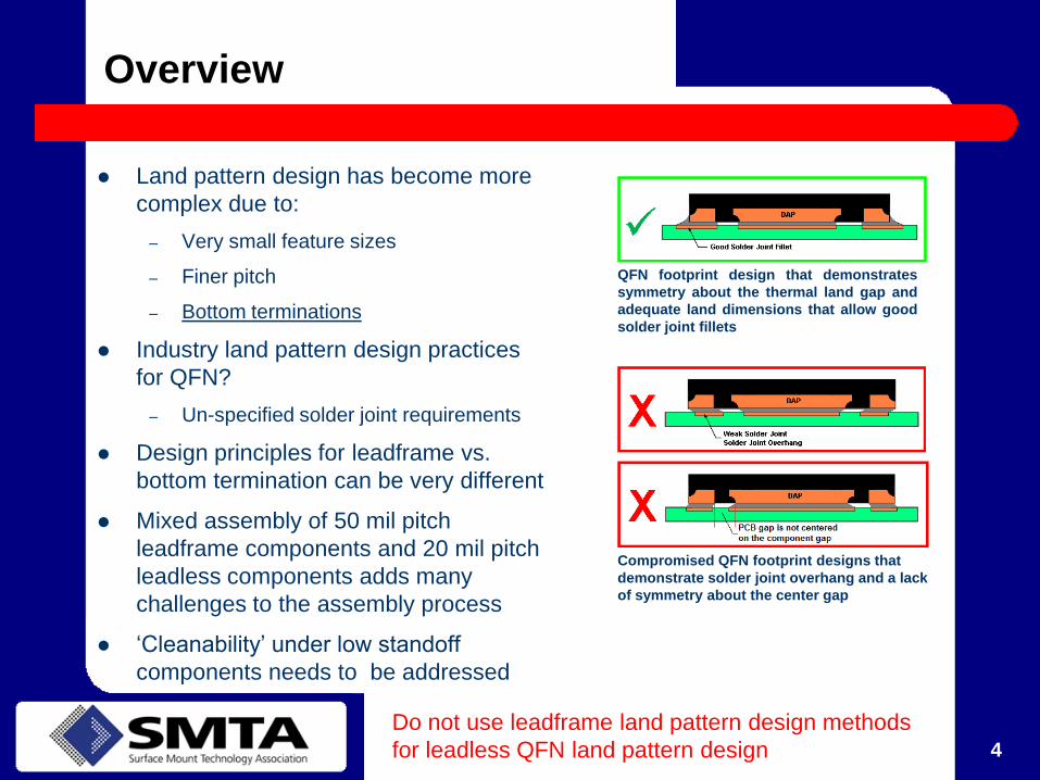
Overview
Land pattern design has become more
complex due to:
– Very small feature sizes
– Finer pitch
– Bottom terminations
Industry land pattern design practices
for QFN?
– Un-specified solder joint requirements
Design principles for leadframe vs.
bottom termination can be very different
Mixed assembly of 50 mil pitch
leadframe components and 20 mil pitch
leadless components adds many
challenges to the assembly process
‘Cleanability’ under low standoff
components needs to be addressed
4
QFN footprint design that demonstrates
symmetry about the thermal land gap and
adequate land dimensions that allow good
solder joint fillets
Compromised QFN footprint designs that
demonstrate solder joint overhang and a lack
of symmetry about the center gap
Do not use leadframe land pattern design methods
for leadless QFN land pattern design

Design Rules / Assumptions
Avoid using solder mask defined (SMD) land pads
Avoid routing peripheral lands to the thermal land
– Route all peripheral lands to vias outside of the land
pattern to minimize solder thieving
– No routes from peripheral lands to the thermal land will
allow using the minimum electrical clearance gap of 8
mils
Avoid shorting lands together within a QFN footprint
– May result in improper, non-coplanar component seating
Do not use solder mask within the QFN land pattern
unless circuit routing to the thermal land is required
Minimum electrical clearance is 8 mils
Standard photo imaging solder mask alignment
allowance is +/- 3 mils
Minimum solder mask web width is 4 mils
PCB fabrication (etch) tolerance is 2 mils
5
Non-preferred land routing
Best practices for land routing

Solder Joint Requirements
For BTC components, solder joint requirements are defined by IPC-7093
Inspection requirements per IPC-610 Class 3 + J-STD-001 Space Addendum
For hi-rel, minimum toe fillet height is unspecified in both IPC-7093 & IPC-610
– Use Class 3 criteria for similar components: solder joint thickness plus 25% of the
termination height
– Land pattern design must account for typical QFN copper lead frame thickness of
approximately 6-8 mils.
– Target value for QFN toe fillet height for high reliability designs is 50% of the
termination height
– Rule of thumb for the toe solder joint length allowance for QFN’s is to extend the land
pad out by at least the amount of the desired total solder joint fillet height
Assuming an 8 mil copper termination thickness (height), a 2-3 mil solder joint
standoff height, and 75% solder wetting height target, an 8 mil land extension
will be used to ensure a good toe fillet
Design the land pattern for symmetry with respect to the component
terminations
6
Solder joint requirements need to be defined for
proper land pattern design
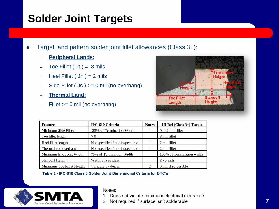
Solder Joint Targets
Target land pattern solder joint fillet allowances (Class 3+):
– Peripheral Lands:
– Toe Fillet ( Jt ) = 8 mils
– Heel Fillet ( Jh ) = 2 mils
– Side Fillet ( Js ) >= 0 mil (no overhang)
– Thermal Land:
– Fillet >= 0 mil (no overhang)
7
Feature IPC-610 Criteria Notes Hi-Rel (Class 3+) Target
Minimum Side Fillet -25% of Termination Width 1 0 to 2 mil fillet
Toe fillet length > 0 8 mil fillet
Heel fillet length Not specified / not inspectable 1 2 mil fillet
Thermal pad overhang Not specified / not inspectable 1 2 mil fillet
Minimum End Joint Width 75% of Termination Width 100% of Termination width
Standoff Height Wetting is evident 2 - 3 mils
Minimum Toe Fillet Height Variable by design 2 6 mil if solderable
Notes:
1. Does not violate minimum electrical clearance
2. Not required if surface isn’t solderable
Table 1 - IPC-610 Class 3 Solder Joint Dimensional Criteria for BTC’s

Land Pattern Design
For high reliability applications, the key to good solder joint reliability is a
robust land pattern design
IPC Class 3 solder joint requirements are a good starting point but
modifications may be required to meet reliability and performance
requirements for the intended end-use environment
For maximum thermal performance, maximizing the thermal land dimensions
is preferred
Fillet ‘wrap-around’ is preferred
Positive fillets preferred
8 Undercut or negative fillets should be avoided
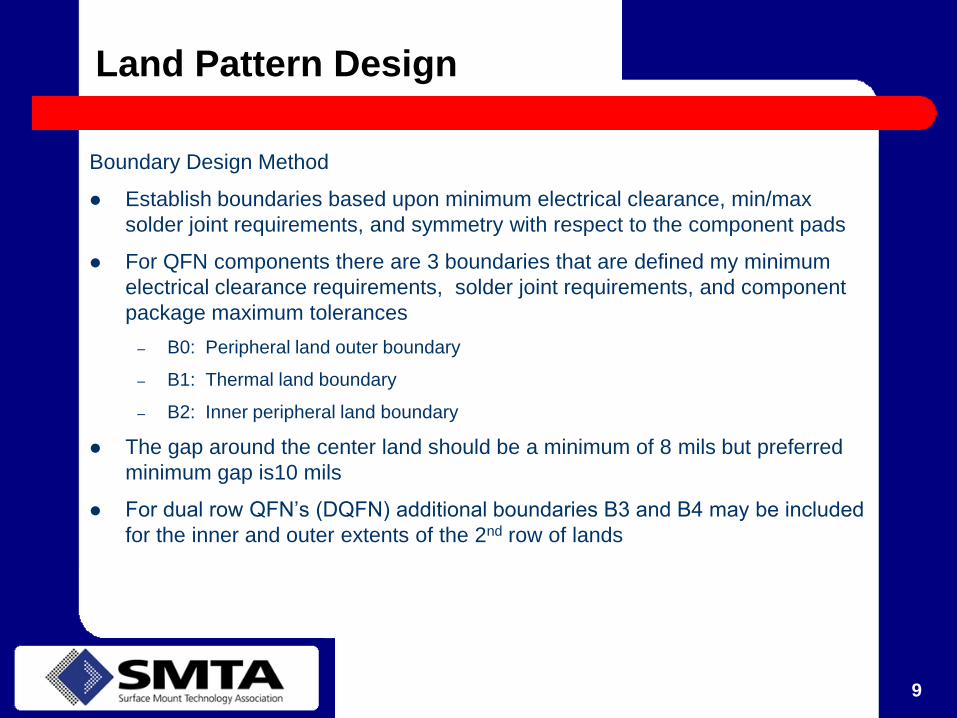
Land Pattern Design
Boundary Design Method
Establish boundaries based upon minimum electrical clearance, min/max
solder joint requirements, and symmetry with respect to the component pads
For QFN components there are 3 boundaries that are defined my minimum
electrical clearance requirements, solder joint requirements, and component
package maximum tolerances
– B0: Peripheral land outer boundary
– B1: Thermal land boundary
– B2: Inner peripheral land boundary
The gap around the center land should be a minimum of 8 mils but preferred
minimum gap is10 mils
For dual row QFN’s (DQFN) additional boundaries B3 and B4 may be included
for the inner and outer extents of the 2nd row of lands
9

Boundaries
10
The outer boundary B0 calculation takes into account:
– Solder joint toe fillet Jt
– PCB etch tolerance F
– Maximum component package dimensions Amax
The thermal land boundary B1 calculation takes into account:
– Symmetry with respect to nominal component package thermal land gap
– Minimum electrical clearance from the inner edge of the peripheral lands
– Maximizing the thermal land for maximum thermal performance
The inner peripheral land boundary B2 calculation takes into account:
– Symmetry with respect to nominal component package thermal land gap
– PCB etch tolerance F
– Minimum electrical clearance with respect to the thermal land
Land pattern design boundaries are based upon
minimum electrical clearance AND solder joint
requirements

Design Steps
1. Determine the nominal centerline of the gap (CLg) between the QFN thermal
pad and the inner edges of the peripheral pads
CLg = (A + Wt)/2 – T – PB
Where:
A = Package dimensions
Wt = Thermal pad dimensions
T = Peripheral pad length
PB = Peripheral pad pullback if applicable
(Standard pullback is 4 mils)
The above equations are based upon the QFN package nominal dimensions
since the goal is to achieve land pattern symmetry with respect to the
component package
11
QFN land pattern design should be symmetric about
the component thermal pad gap

Design Steps
2. Establish the 3 land pattern boundaries
The peripheral land outer boundary:
B0 = Amax + 2*Jt – 2*PB + F
The thermal land boundary:
B1 = CLg – Wg
The peripheral land inner boundary:
B2 = CLg + Wg
Simplify the boundary equations for the
known/desired values:
Wg = 10 mils preferred, 8 mils minimum
Jt = 8 mils (Solder joint toe fillet)
F = 2 mils (PCB etch tolerance)
B0 = Amax – 2*PB + 18 mils
B1 = CLg – 10 mils
B2 = CLg + 10 mils
12

Design Steps
3. Calculate the thermal land dimensions:
X2 = Wtmax or B1 whichever is less
Where: Wtmax = Maximum QFN thermal
pad dimension
4. Calculate the inner edge of the
peripheral lands:
Y1in = B2 + (B1 – X2)
5. The peripheral land length is:
Y1= (B0 – Y1in) / 2
13

Design Steps
6. The peripheral land width X1 is a function of pitch and should allow for a
positive side fillet (Js>=0) if possible
X1 = Wmax + F or Xmax whichever is less
Where:
F = PCB etch tolerance = 2 mils
Wmax = Maximum QFN peripheral pad width
Xmax = Maximum PCB land width per Table 2
Note: Minimum electrical clearance Cle must change from 8 mils to 6 mils for 0.4mm pitch
14
Pitch PCB
Xmax
Typical
Wmax
mm mils mils mils
0.8 30 17 16
0.65 25 15 14
0.5 20 11 12
0.4 16 10 10
Table 2 – Maximum PCB land widths
Xmax and typical maximum component
pad dimensions Wmax

Design Steps
7. The center-to-center spacing of the peripheral lands on opposite sides of the
land pattern, also known as padstack (S), is calculated as follows:
S = B0 – Y1
15
We’re done with design - No more equations!

Solder Mask Considerations
Robust QFN land pattern design excludes the use of solder mask within the
footprint for the following reasons:
16
1. Solder mask defined pads (SMD) may
create a stress riser on solder joints that can
lead to solder joint cracking and premature
failure
2. Non solder mask defined pads (NSMD)
allow the solder to wrap around the sides of
the PCB lands and improves reliability
3. Due to the low standoff height of QFN’s, it is
preferred to maximize the under-component
gap in order to maximize cleaning efficiency
• Effective cleaning gap increases by
the thickness of the solder mask
• Solder mask over traces makes the
gap even smaller
4. Flux residues left underneath QFN
component packages may lead to corrosion
or electro-migration related failures
Maximize the gap by removing the solder mask
X X X
Avoid using solder mask within a QFN land pattern for
maximum cleanability and solder joint reliability

Flux Entrapment / Cleaning
If routing of peripheral lands to the thermal land cannot be avoided then solder
mask stripes should be applied only over the circuit lines and not around the
entire thermal pad (window pane)
Do not solder mask define the thermal land
17
Flux has been allowed to escape from the thermal land
solder joint
Example of solder mask stripes instead of
‘window pane’
Flux

Thermal Vias
The preferred via structure for high
reliability applications is the IPC type VII
filled and over-plated via
Use a fill material that is thermally
conductive with very low shrinkage to
minimize via dimples which can trap flux
and cause voiding
Fill material CTE should closely match the
PCB material CTE
Use only outgas compliant materials
(typically stated as 100% solids content)
18
Vias can be open or filled, covered with solder mask, over-plated, or even
plated shut
Open vias should be avoided for hi-rel designs
May cause lower standoff height due to solder wicking down the vias
Partially solder filled vias may lead to via cracking during thermal cycling
IPC Type VII Filled and Over-plated Via

Stencil Design
Reduce the solder paste area coverage for
the thermal land by approximately 1/3
Print peripheral lands 1:1 with the PCB lands
Solder stencil void reduction methods
– 5 mil solder stencil thickness is typically
sufficient – thicker may result in more voids
due to more flux
– Avoid printing solder paste directly over the
center of vias where a dimple is likely
– For the thermal land, window pane or cross
hatch solder deposits should not be spaced
more than 10 mils apart
– Use a 45o cross hatch pattern for the thermal
land instead of window pane to promote flux
escape from the solder joint (no intersections)
– If window pane design is used, minimize the
number of window pane intersections
19
Voids that resulted from improper
window pane solder stencil design
45o 8 x 16 mil solder stencil crosshatch
pattern

Solder Paste & Reflow
Solder Paste
Solder paste can have a significant impact
on voiding in QFN thermal land solder joints,
especially for rosin-based, low activity solder
pastes typically used for hi-rel assembly
Use a low solids ‘no-clean’ type solder paste
– Flux activity, composition, and activator
chemistry may also impact voiding
Reflow Profile
Reflow profile is typically dictated by other
more massive components
A ‘soak’ profile is usually best for void
minimization but use caution not to go
beyond flux activity limits
Nitrogen atmosphere to reduce oxidation
20
Flux induced voids
It is a good idea to re-qualify your solder paste for void
reduction and solderability with respect to QFN assembly
Voids caused by flux and oxide entrapment

Component Plating Concerns
Gold and other noble metals such as silver
and palladium may cause solder joint
embrittlement, especially in low volume,
low standoff QFN solder joints
– Avoid or remove these plating materials
prior to assembly
For high reliability applications, if a gold
plating is any other than immersion gold, it
should be removed prior to soldering as
documented by J-STD-001, section 4.5
– Double tin and wick or dynamic wave
removal processes are the correct methods
for plating removal / replacement
IPC-7093, Section 8.2.6 provides guidance
with respect solder joint embrittlement
avoidance
21
Gold Embrittlement in a QFN solder joint
Confirm immersion gold plating or remove gold from
QFN components prior to assembly

Recommendations
Follow hi-rel best practices for design rules and allowances
Use the boundary design method to achieve:
– Land sizes that will allow for adequate solder joint height and fillets
– Land pattern symmetry with respect to the QFN package terminations
– 10 mil gap around thermal land preferred, 8 mil minimum
Use IPC Class 3+ for solder joint allowances
– Toe Fillet ( Jt ) = 8 mils
– Heel Fillet ( Jh ) = 2 mils
– Side Fillet ( Js ) >= 0 mil (no overhang)
Best practices for stencil design
– Reduce the solder paste area coverage for the thermal land by approximately 1/3
– Use a 45o cross hatch pattern for the thermal land instead of window pane
Use a solder paste that is optimized for your QFN soldering process
– Use a low solids ‘no-clean’ type solder paste with good oxide reducing activators
– A solder paste requalification for BTC void reduction is recommended
22
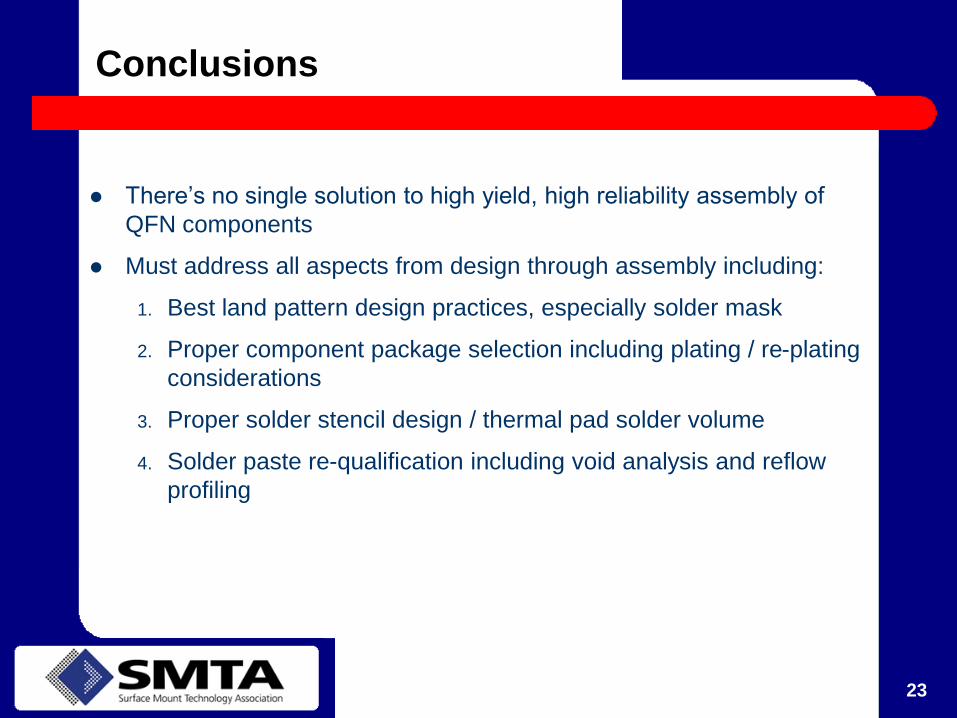
Conclusions
There’s no single solution to high yield, high reliability assembly of
QFN components
Must address all aspects from design through assembly including:
1. Best land pattern design practices, especially solder mask
2. Proper component package selection including plating / re-plating
considerations
3. Proper solder stencil design / thermal pad solder volume
4. Solder paste re-qualification including void analysis and reflow
profiling
23
References
1. IPC-7093, Design and Assembly Process Implementation for Bottom
Termination Components, March 2011
2. IPC-A-610, Acceptability of Electronic Assemblies, February 2005
3. IPC-7351, Generic Requirements for Surface Mount Design and Land Pattern
Standard, June 2010
4. IPC-7535, Stencil Design Guidelines, October 2011
5. J-STD-001, Requirements for Soldered Electrical and Electronic Assemblies,
April 2010
6. IPC-9202, Material and Process Characterization / Qualification Test Protocol
For Assessing Electrochemical Performance, October 2011
24

Q & A
Questions
25