Embed Size (px)
Citation preview

1
2
3
4
5
6
7
8
9
10
20
19
18
17
16
15
14
13
12
11
OE1
A1
A2
A3
A4
A5
A6
A7
A8
GND
VCC
OE2
Y1
Y2
Y3
Y4
Y5
Y6
Y7
Y8
SN74AHCT541 . . . DB, DGV, DW, N, NS, OR PW PACKAGE
(TOP VIEW)
3 2 1 20 19
9 10 11 12 13
4
5
6
7
8
18
17
16
15
14
Y1
Y2
Y3
Y4
Y5
A3
A4
A5
A6
A7
SN54AHCT541 . . . FK PACKAGE
(TOP VIEW)
A2
A1
OE
1
Y7
Y6
OE
2
A8
GN
D
Y8
VC
C
SN54AHCT541 . . . J or W PACKAGE
SN54AHCT541SN74AHCT541
www.ti.com SCLS269P –OCTOBER 1995–REVISED JUNE 2013
OCTAL BUFFERS/DRIVERS WITH 3-STATE OUTPUTSCheck for Samples: SN54AHCT541, SN74AHCT541
1FEATURES• Inputs Are TTL-Voltage Compatible• Latch-Up Performance Exceeds 250 mA Per
JESD 17• ESD Protection Exceeds JESD 22
– 2000-V Human-Body Model (A114-A)– 200-V Machine Model (A115-A)– 1000-V Charged-Device Model (C101)
DESCRIPTIONThe ’AHCT541 octal buffers/drivers are ideal fordriving bus lines or buffer memory address registers.These devices feature inputs and outputs on oppositesides of the package to facilitate printed circuit boardlayout.
The 3-state control gate is a 2-input AND gate withactive-low inputs so that if either output-enable (OE1or OE2) input is high, all corresponding outputs are inthe high-impedance state. The outputs provide non-inverted data when they are not in the high-impedance state.
To ensure the high-impedance state during power upor power down, OE should be tied to VCC through apullup resistor; the minimum value of the resistor isdetermined by the current-sinking capability of thedriver.
FUNCTION TABLE(EACH FLIP-FLOP)
INPUTS OUTPUTOE1 OE2 AY
L L L L
L L H H
H X X Z
X H X Z
1
Please be aware that an important notice concerning availability, standard warranty, and use in critical applications ofTexas Instruments semiconductor products and disclaimers thereto appears at the end of this data sheet.
PRODUCTION DATA information is current as of publication date. Copyright © 1995–2013, Texas Instruments IncorporatedProducts conform to specifications per the terms of the TexasInstruments standard warranty. Production processing does notnecessarily include testing of all parameters.
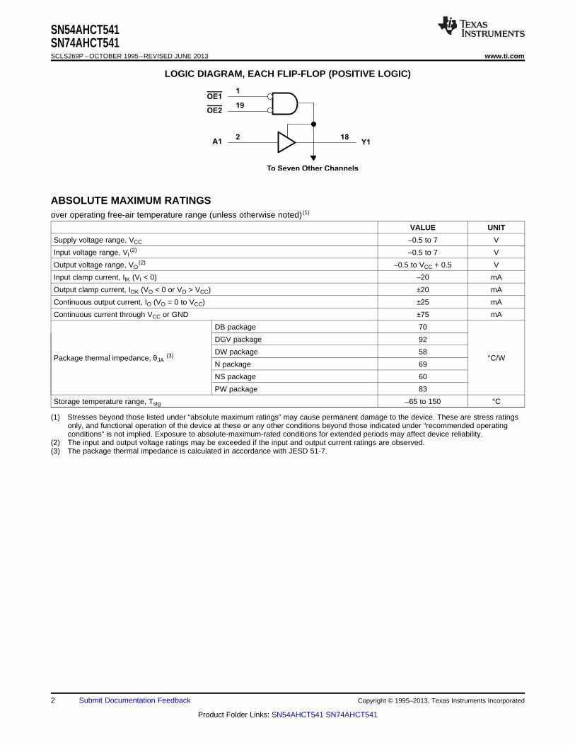
OE1
OE2
To Seven Other Channels
A1 Y1
1
19
2 18
SN54AHCT541SN74AHCT541SCLS269P –OCTOBER 1995–REVISED JUNE 2013 www.ti.com
LOGIC DIAGRAM, EACH FLIP-FLOP (POSITIVE LOGIC)
ABSOLUTE MAXIMUM RATINGSover operating free-air temperature range (unless otherwise noted) (1)
VALUE UNIT
Supply voltage range, VCC –0.5 to 7 V
Input voltage range, VI(2) –0.5 to 7 V
Output voltage range, VO(2) –0.5 to VCC + 0.5 V
Input clamp current, IIK (VI < 0) –20 mA
Output clamp current, IOK (VO < 0 or VO > VCC) ±20 mA
Continuous output current, IO (VO = 0 to VCC) ±25 mA
Continuous current through VCC or GND ±75 mA
DB package 70
DGV package 92
DW package 58Package thermal impedance, θJA
(3) °C/WN package 69
NS package 60
PW package 83
Storage temperature range, Tstg –65 to 150 °C
(1) Stresses beyond those listed under “absolute maximum ratings” may cause permanent damage to the device. These are stress ratingsonly, and functional operation of the device at these or any other conditions beyond those indicated under “recommended operatingconditions” is not implied. Exposure to absolute-maximum-rated conditions for extended periods may affect device reliability.
(2) The input and output voltage ratings may be exceeded if the input and output current ratings are observed.(3) The package thermal impedance is calculated in accordance with JESD 51-7.
2 Submit Documentation Feedback Copyright © 1995–2013, Texas Instruments Incorporated
Product Folder Links: SN54AHCT541 SN74AHCT541

SN54AHCT541SN74AHCT541
www.ti.com SCLS269P –OCTOBER 1995–REVISED JUNE 2013
RECOMMENDED OPERATING CONDITIONS (1)
SN54AHCT541 SN74AHCT541UNIT
MIN MAX MIN MAX
VCC Supply voltage 4.5 5.5 4.5 5.5 V
VIH High-level input voltage 2 2 V
VIL Low-level Input voltage 0.8 0.8 V
VI Input voltage 0 5.5 0 5.5 V
VO Output voltage 0 VCC 0 VCC V
IOH High-level output current –8 –8 mA
IOL Low-level output current 8 8 mA
Δt/Δv Input Transition rise or fall rate 20 20 ns/V
TA Operating free-air temperature –55 125 –40 125 °C
(1) All unused inputs of the device must be held at VCC or GND to ensure proper device operation. Refer to the TI application report,Implications of Slow or Floating CMOS Inputs, literature number SCBA004.
ELECTRICAL CHARACTERISTICSover operating free-air temperature range (unless otherwise noted)
TA = –40°C TOTA = –55°C TO TA = –40°C TO 125°C
125°C 85°CTA = 25°C RecommendedPARAMETER TEST CONDITIONS VCC UNITSN54AHCT541 SN74AHCT541 SN74AHCT541
MIN TYP MAX MIN MAX MIN MAX MIN MAX
IOH = –50 µA 4.4 4.5 4.4 4.4 4.4VOH 4.5 V V
IOH = –8 mA 3.94 3.8 3.8 3.8
IOL = 50 µA 0.1 0.1 0.1 0.1VOL 4.5 V V
IOH = 8 mA 0.36 0.44 0.44 0.44
0 V to 5.5II VI = 5.5 V or GND ±0.1 ±1 (1) ±1 ±1 µAV
IOZ VO = VCC or GND 5.5 V ±0.25 ±2.5 ±2.5 ±2.5
VI = VCC orICC IO = 0 5.5 V 4 40 20 40 µAGND,
One input at 3.4 V,ΔICC
(2) Other inputs at VCC or 5.5 V 1.35 1.5 1.5 1.5 mAGND
Ci VI = VCC or GND 5 V 2 10 10 pF
CO VO = VCC or GND 5V 4
(1) On products compliant to MIL-PRF-38535, this parameter is not production tested at VCC = 0 V.(2) This is the increase in supply current for each input at one of the specified TTL voltage levels, rather than 0 V or VCC.
Copyright © 1995–2013, Texas Instruments Incorporated Submit Documentation Feedback 3
Product Folder Links: SN54AHCT541 SN74AHCT541

SN54AHCT541SN74AHCT541SCLS269P –OCTOBER 1995–REVISED JUNE 2013 www.ti.com
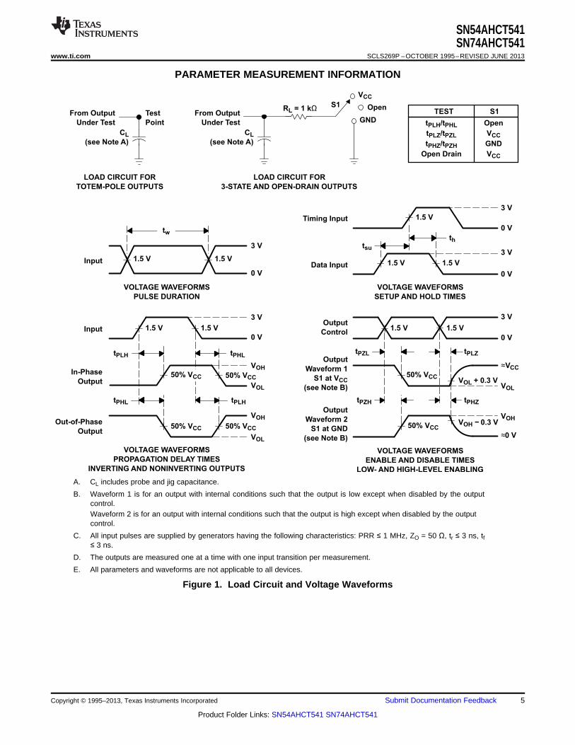
SWITCHING CHARACTERISTICSover recommended operating free-air temperature range, VCC = 5 V ± 0.5 V (unless otherwise noted) (see Figure 1)
TA = –40°C TOTA = –55°C TO TA = –40°C TO 125°C
125°C 85°CTA = 25°CFROM TO LOAD RecommendedPARAMETER UNIT(INPUT) (OUTPUT) CAPACITANCESN54AHCT541 SN54AHCT541 SN54AHCT541
TYP MAX MIN MAX MIN MAX MIN MAX
tPLH 4.1 (1) 6.0 (1) 1 (1) 6.5 (1) 1 6.5 1 6.5A Y CL = 15 pF ns
tPHL 4.1 (1) 6.0 (1) 1 (1) 6.5 (1) 1 6.5 1 6.5
tPZH 5.0 (1) 7.0 (1) 1 (1) 8.0 (1) 1 8.0 1 8.0OE Y CL = 15 pF ns
tPZL 5.0 (1) 7.0 (1) 1 (1) 8.0 (1) 1 8.0 1 8.0
tPHZ 4.5 (1) 7.0 (1) 1 (1) 8.0 (1) 1 8.0 1 8.0OE Y CL = 15 pF ns
tPLZ 4.5 (1) 7.0 (1) 1 (1) 8.0 (1) 1 8.0 1 8.0
tPLH 6.2 8.5 1 9.5 1 9.5 1 9.5A Y CL = 50 pF ns
tPHL 6.2 8.5 1 9.5 1 9.5 1 9.5
tPZH 7.5 10.0 1 12 1 12 1 12OE Y CL = 50 pF ns
tPZL 7.5 10.0 1 12 1 12 1 12
tPHZ 7.0 10.0 1 12 1 12 1 12OE Y CL = 50 pF ns
tPLZ 7.0 10.0 1 12 1 12 1 12
tsk(o) CL = 50 pF 1 (2) 1 1
(1) On products compliant to MIL-PRF-38535, this parameter is not production tested.(2) On products compliant to MIL-PRF-38535, this parameter does not apply
OPERATING CHARACTERISTICSVCC = 5 V, TA = 25°C
PARAMETER TEST CONDITIONS TYP UNIT
Cpd Power dissipation capacitance No load, f = 1 MHz 12 pF
4 Submit Documentation Feedback Copyright © 1995–2013, Texas Instruments Incorporated
Product Folder Links: SN54AHCT541 SN74AHCT541
50% VCC
3 V
3 V
0 V
0 V
thtsu
VOLTAGE WAVEFORMS
SETUP AND HOLD TIMES
Data Input
tPLH
tPHL
tPHL
tPLH
VOH
VOH
VOL
VOL
3 V
0 V
50% VCC50% VCC
Input
Out-of-Phase
Output
In-Phase
Output
Timing Input
50% VCC
VOLTAGE WAVEFORMS
PROPAGATION DELAY TIMES
INVERTING AND NONINVERTING OUTPUTS
Output
Control
Output
Waveform 1
S1 at VCC
(see Note B)
Output
Waveform 2
S1 at GND
(see Note B)
VOL
VOH
tPZL
tPZH
tPLZ
tPHZ
≈VCC
0 V
50% VCCVOL + 0.3 V
50% VCC
≈0 V
3 V
VOLTAGE WAVEFORMS
ENABLE AND DISABLE TIMES
LOW- AND HIGH-LEVEL ENABLING
tPLH/tPHL
tPLZ/tPZL
tPHZ/tPZH
Open Drain
Open
VCC
GND
VCC
TEST S1
3 V
0 V
tw
VOLTAGE WAVEFORMS
PULSE DURATION
Input
From Output
Under Test
CL
(see Note A)
LOAD CIRCUIT FOR
3-STATE AND OPEN-DRAIN OUTPUTS
S1
VCC
RL = 1 kΩ
GNDFrom Output
Under Test
CL
(see Note A)
Test
Point
LOAD CIRCUIT FOR
TOTEM-POLE OUTPUTS
Open
VOH − 0.3 V
1.5 V 1.5 V
1.5 V
1.5 V 1.5 V
1.5 V 1.5 V1.5 V 1.5 V
SN54AHCT541SN74AHCT541
www.ti.com SCLS269P –OCTOBER 1995–REVISED JUNE 2013
PARAMETER MEASUREMENT INFORMATION
A. CL includes probe and jig capacitance.
B. Waveform 1 is for an output with internal conditions such that the output is low except when disabled by the outputcontrol.Waveform 2 is for an output with internal conditions such that the output is high except when disabled by the outputcontrol.
C. All input pulses are supplied by generators having the following characteristics: PRR ≤ 1 MHz, ZO = 50 Ω, tr ≤ 3 ns, tf≤ 3 ns.
D. The outputs are measured one at a time with one input transition per measurement.
E. All parameters and waveforms are not applicable to all devices.
Figure 1. Load Circuit and Voltage Waveforms
Copyright © 1995–2013, Texas Instruments Incorporated Submit Documentation Feedback 5
Product Folder Links: SN54AHCT541 SN74AHCT541

SN54AHCT541SN74AHCT541SCLS269P –OCTOBER 1995–REVISED JUNE 2013 www.ti.com
REVISION HISTORY
Changes from Revision O (July 2003) to Revision P Page
• Changed document format from Quicksilver to DocZone. .................................................................................................... 1
• Extended operating temperature range to 125°C ................................................................................................................. 3
6 Submit Documentation Feedback Copyright © 1995–2013, Texas Instruments Incorporated
Product Folder Links: SN54AHCT541 SN74AHCT541

PACKAGE OPTION ADDENDUM
www.ti.com 17-Mar-2017
Addendum-Page 1
PACKAGING INFORMATION
Orderable Device Status(1)
Package Type PackageDrawing
Pins PackageQty
Eco Plan(2)
Lead/Ball Finish(6)
MSL Peak Temp(3)
Op Temp (°C) Device Marking(4/5)
Samples
5962-9685801Q2A ACTIVE LCCC FK 20 1 TBD POST-PLATE N / A for Pkg Type -55 to 125 5962-9685801Q2ASNJ54AHCT541FK
5962-9685801QRA ACTIVE CDIP J 20 1 TBD A42 N / A for Pkg Type -55 to 125 5962-9685801QRASNJ54AHCT541J
5962-9685801QSA ACTIVE CFP W 20 1 TBD A42 N / A for Pkg Type -55 to 125 5962-9685801QSASNJ54AHCT541W
SN74AHCT541DBR ACTIVE SSOP DB 20 2000 Green (RoHS& no Sb/Br)
CU NIPDAU Level-1-260C-UNLIM -40 to 125 HB541
SN74AHCT541DBRE4 ACTIVE SSOP DB 20 2000 Green (RoHS& no Sb/Br)
CU NIPDAU Level-1-260C-UNLIM -40 to 125 HB541
SN74AHCT541DW ACTIVE SOIC DW 20 25 Green (RoHS& no Sb/Br)
CU NIPDAU Level-1-260C-UNLIM -40 to 125 AHCT541
SN74AHCT541DWG4 ACTIVE SOIC DW 20 25 Green (RoHS& no Sb/Br)
CU NIPDAU Level-1-260C-UNLIM -40 to 125 AHCT541
SN74AHCT541DWR ACTIVE SOIC DW 20 2000 Green (RoHS& no Sb/Br)
CU NIPDAU Level-1-260C-UNLIM -40 to 125 AHCT541
SN74AHCT541DWRE4 ACTIVE SOIC DW 20 2000 Green (RoHS& no Sb/Br)
CU NIPDAU Level-1-260C-UNLIM -40 to 125 AHCT541
SN74AHCT541N ACTIVE PDIP N 20 20 Pb-Free(RoHS)
CU NIPDAU N / A for Pkg Type -40 to 125 SN74AHCT541N
SN74AHCT541NSR ACTIVE SO NS 20 2000 Green (RoHS& no Sb/Br)
CU NIPDAU Level-1-260C-UNLIM -40 to 125 AHCT541
SN74AHCT541PW ACTIVE TSSOP PW 20 70 Green (RoHS& no Sb/Br)
CU NIPDAU Level-1-260C-UNLIM -40 to 125 HB541
SN74AHCT541PWE4 ACTIVE TSSOP PW 20 70 Green (RoHS& no Sb/Br)
CU NIPDAU Level-1-260C-UNLIM -40 to 125 HB541
SN74AHCT541PWG4 ACTIVE TSSOP PW 20 70 Green (RoHS& no Sb/Br)
CU NIPDAU Level-1-260C-UNLIM -40 to 125 HB541
SN74AHCT541PWR ACTIVE TSSOP PW 20 2000 Green (RoHS& no Sb/Br)
CU NIPDAU | CU SN Level-1-260C-UNLIM -40 to 125 HB541

PACKAGE OPTION ADDENDUM
www.ti.com 17-Mar-2017
Addendum-Page 2
Orderable Device Status(1)
Package Type PackageDrawing
Pins PackageQty
Eco Plan(2)
Lead/Ball Finish(6)
MSL Peak Temp(3)
Op Temp (°C) Device Marking(4/5)
Samples
SN74AHCT541PWRE4 ACTIVE TSSOP PW 20 2000 Green (RoHS& no Sb/Br)
CU NIPDAU Level-1-260C-UNLIM -40 to 125 HB541
SN74AHCT541PWRG3 ACTIVE TSSOP PW 20 2000 Green (RoHS& no Sb/Br)
CU SN Level-1-260C-UNLIM -40 to 125 HB541
SN74AHCT541PWRG4 ACTIVE TSSOP PW 20 2000 Green (RoHS& no Sb/Br)
CU NIPDAU Level-1-260C-UNLIM -40 to 125 HB541
SNJ54AHCT541FK ACTIVE LCCC FK 20 1 TBD POST-PLATE N / A for Pkg Type -55 to 125 5962-9685801Q2ASNJ54AHCT541FK
SNJ54AHCT541J ACTIVE CDIP J 20 1 TBD A42 N / A for Pkg Type -55 to 125 5962-9685801QRASNJ54AHCT541J
SNJ54AHCT541W ACTIVE CFP W 20 1 TBD A42 N / A for Pkg Type -55 to 125 5962-9685801QSASNJ54AHCT541W
(1) The marketing status values are defined as follows:ACTIVE: Product device recommended for new designs.LIFEBUY: TI has announced that the device will be discontinued, and a lifetime-buy period is in effect.NRND: Not recommended for new designs. Device is in production to support existing customers, but TI does not recommend using this part in a new design.PREVIEW: Device has been announced but is not in production. Samples may or may not be available.OBSOLETE: TI has discontinued the production of the device.
(2) Eco Plan - The planned eco-friendly classification: Pb-Free (RoHS), Pb-Free (RoHS Exempt), or Green (RoHS & no Sb/Br) - please check http://www.ti.com/productcontent for the latest availabilityinformation and additional product content details.TBD: The Pb-Free/Green conversion plan has not been defined.Pb-Free (RoHS): TI's terms "Lead-Free" or "Pb-Free" mean semiconductor products that are compatible with the current RoHS requirements for all 6 substances, including the requirement thatlead not exceed 0.1% by weight in homogeneous materials. Where designed to be soldered at high temperatures, TI Pb-Free products are suitable for use in specified lead-free processes.Pb-Free (RoHS Exempt): This component has a RoHS exemption for either 1) lead-based flip-chip solder bumps used between the die and package, or 2) lead-based die adhesive used betweenthe die and leadframe. The component is otherwise considered Pb-Free (RoHS compatible) as defined above.Green (RoHS & no Sb/Br): TI defines "Green" to mean Pb-Free (RoHS compatible), and free of Bromine (Br) and Antimony (Sb) based flame retardants (Br or Sb do not exceed 0.1% by weightin homogeneous material)
(3) MSL, Peak Temp. - The Moisture Sensitivity Level rating according to the JEDEC industry standard classifications, and peak solder temperature.
(4) There may be additional marking, which relates to the logo, the lot trace code information, or the environmental category on the device.

PACKAGE OPTION ADDENDUM
www.ti.com 17-Mar-2017
Addendum-Page 3
(5) Multiple Device Markings will be inside parentheses. Only one Device Marking contained in parentheses and separated by a "~" will appear on a device. If a line is indented then it is a continuationof the previous line and the two combined represent the entire Device Marking for that device.
(6) Lead/Ball Finish - Orderable Devices may have multiple material finish options. Finish options are separated by a vertical ruled line. Lead/Ball Finish values may wrap to two lines if the finishvalue exceeds the maximum column width.
Important Information and Disclaimer:The information provided on this page represents TI's knowledge and belief as of the date that it is provided. TI bases its knowledge and belief on informationprovided by third parties, and makes no representation or warranty as to the accuracy of such information. Efforts are underway to better integrate information from third parties. TI has taken andcontinues to take reasonable steps to provide representative and accurate information but may not have conducted destructive testing or chemical analysis on incoming materials and chemicals.TI and TI suppliers consider certain information to be proprietary, and thus CAS numbers and other limited information may not be available for release.
In no event shall TI's liability arising out of such information exceed the total purchase price of the TI part(s) at issue in this document sold by TI to Customer on an annual basis.
OTHER QUALIFIED VERSIONS OF SN54AHCT541, SN74AHCT541 :
• Catalog: SN74AHCT541
• Enhanced Product: SN74AHCT541-EP, SN74AHCT541-EP
• Military: SN54AHCT541
NOTE: Qualified Version Definitions:
• Catalog - TI's standard catalog product
• Enhanced Product - Supports Defense, Aerospace and Medical Applications
• Military - QML certified for Military and Defense Applications
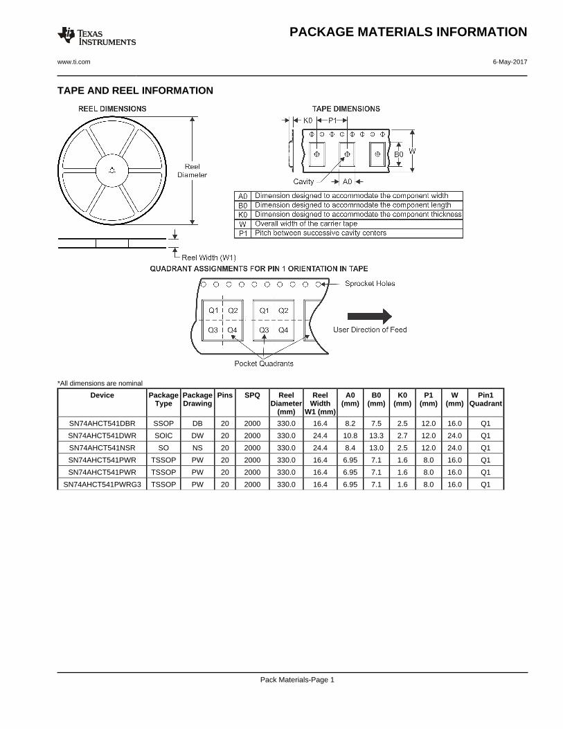
TAPE AND REEL INFORMATION
*All dimensions are nominal
Device PackageType
PackageDrawing
Pins SPQ ReelDiameter
(mm)
ReelWidth
W1 (mm)
A0(mm)
B0(mm)
K0(mm)
P1(mm)
W(mm)
Pin1Quadrant
SN74AHCT541DBR SSOP DB 20 2000 330.0 16.4 8.2 7.5 2.5 12.0 16.0 Q1
SN74AHCT541DWR SOIC DW 20 2000 330.0 24.4 10.8 13.3 2.7 12.0 24.0 Q1
SN74AHCT541NSR SO NS 20 2000 330.0 24.4 8.4 13.0 2.5 12.0 24.0 Q1
SN74AHCT541PWR TSSOP PW 20 2000 330.0 16.4 6.95 7.1 1.6 8.0 16.0 Q1
SN74AHCT541PWR TSSOP PW 20 2000 330.0 16.4 6.95 7.1 1.6 8.0 16.0 Q1
SN74AHCT541PWRG3 TSSOP PW 20 2000 330.0 16.4 6.95 7.1 1.6 8.0 16.0 Q1
PACKAGE MATERIALS INFORMATION
www.ti.com 6-May-2017
Pack Materials-Page 1

*All dimensions are nominal
Device Package Type Package Drawing Pins SPQ Length (mm) Width (mm) Height (mm)
SN74AHCT541DBR SSOP DB 20 2000 367.0 367.0 38.0
SN74AHCT541DWR SOIC DW 20 2000 367.0 367.0 45.0
SN74AHCT541NSR SO NS 20 2000 367.0 367.0 45.0
SN74AHCT541PWR TSSOP PW 20 2000 367.0 367.0 38.0
SN74AHCT541PWR TSSOP PW 20 2000 364.0 364.0 27.0
SN74AHCT541PWRG3 TSSOP PW 20 2000 364.0 364.0 27.0
PACKAGE MATERIALS INFORMATION
www.ti.com 6-May-2017
Pack Materials-Page 2


MECHANICAL DATA
MSSO002E – JANUARY 1995 – REVISED DECEMBER 2001
POST OFFICE BOX 655303 • DALLAS, TEXAS 75265
DB (R-PDSO-G**) PLASTIC SMALL-OUTLINE
4040065 /E 12/01
28 PINS SHOWN
Gage Plane
8,207,40
0,550,95
0,25
38
12,90
12,30
28
10,50
24
8,50
Seating Plane
9,907,90
30
10,50
9,90
0,38
5,605,00
15
0,22
14
A
28
1
2016
6,506,50
14
0,05 MIN
5,905,90
DIM
A MAX
A MIN
PINS **
2,00 MAX
6,90
7,50
0,65 M0,15
0°–8°
0,10
0,090,25
NOTES: A. All linear dimensions are in millimeters.B. This drawing is subject to change without notice.C. Body dimensions do not include mold flash or protrusion not to exceed 0,15.D. Falls within JEDEC MO-150


www.ti.com
PACKAGE OUTLINE
C
TYP10.639.97
2.65 MAX
18X 1.27
20X 0.510.31
2X11.43
TYP0.330.10
0 - 80.30.1
0.25GAGE PLANE
1.270.40
A
NOTE 3
13.012.6
B 7.67.4
4220724/A 05/2016
SOIC - 2.65 mm max heightDW0020ASOIC
NOTES: 1. All linear dimensions are in millimeters. Dimensions in parenthesis are for reference only. Dimensioning and tolerancing per ASME Y14.5M. 2. This drawing is subject to change without notice. 3. This dimension does not include mold flash, protrusions, or gate burrs. Mold flash, protrusions, or gate burrs shall not exceed 0.15 mm per side. 4. This dimension does not include interlead flash. Interlead flash shall not exceed 0.43 mm per side.5. Reference JEDEC registration MS-013.
120
0.25 C A B
1110
PIN 1 IDAREA
NOTE 4
SEATING PLANE
0.1 C
SEE DETAIL A
DETAIL ATYPICAL
SCALE 1.200

www.ti.com
EXAMPLE BOARD LAYOUT
(9.3)
0.07 MAXALL AROUND
0.07 MINALL AROUND
20X (2)
20X (0.6)
18X (1.27)
(R )TYP
0.05
4220724/A 05/2016
SOIC - 2.65 mm max heightDW0020ASOIC
SYMM
SYMM
LAND PATTERN EXAMPLESCALE:6X
1
10 11
20
NOTES: (continued) 6. Publication IPC-7351 may have alternate designs. 7. Solder mask tolerances between and around signal pads can vary based on board fabrication site.
METALSOLDER MASKOPENING
NON SOLDER MASKDEFINED
SOLDER MASK DETAILS
SOLDER MASKOPENING
METAL UNDERSOLDER MASK
SOLDER MASKDEFINED
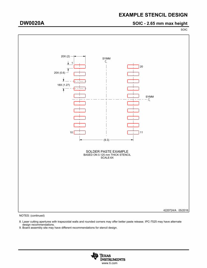
www.ti.com
EXAMPLE STENCIL DESIGN
(9.3)
18X (1.27)
20X (0.6)
20X (2)
4220724/A 05/2016
SOIC - 2.65 mm max heightDW0020ASOIC
NOTES: (continued) 8. Laser cutting apertures with trapezoidal walls and rounded corners may offer better paste release. IPC-7525 may have alternate design recommendations. 9. Board assembly site may have different recommendations for stencil design.
SYMM
SYMM
1
10 11
20
SOLDER PASTE EXAMPLEBASED ON 0.125 mm THICK STENCIL
SCALE:6X

IMPORTANT NOTICE
Texas Instruments Incorporated (TI) reserves the right to make corrections, enhancements, improvements and other changes to itssemiconductor products and services per JESD46, latest issue, and to discontinue any product or service per JESD48, latest issue. Buyersshould obtain the latest relevant information before placing orders and should verify that such information is current and complete.TI’s published terms of sale for semiconductor products (http://www.ti.com/sc/docs/stdterms.htm) apply to the sale of packaged integratedcircuit products that TI has qualified and released to market. Additional terms may apply to the use or sale of other types of TI products andservices.Reproduction of significant portions of TI information in TI data sheets is permissible only if reproduction is without alteration and isaccompanied by all associated warranties, conditions, limitations, and notices. TI is not responsible or liable for such reproduceddocumentation. Information of third parties may be subject to additional restrictions. Resale of TI products or services with statementsdifferent from or beyond the parameters stated by TI for that product or service voids all express and any implied warranties for theassociated TI product or service and is an unfair and deceptive business practice. TI is not responsible or liable for any such statements.Buyers and others who are developing systems that incorporate TI products (collectively, “Designers”) understand and agree that Designersremain responsible for using their independent analysis, evaluation and judgment in designing their applications and that Designers havefull and exclusive responsibility to assure the safety of Designers' applications and compliance of their applications (and of all TI productsused in or for Designers’ applications) with all applicable regulations, laws and other applicable requirements. Designer represents that, withrespect to their applications, Designer has all the necessary expertise to create and implement safeguards that (1) anticipate dangerousconsequences of failures, (2) monitor failures and their consequences, and (3) lessen the likelihood of failures that might cause harm andtake appropriate actions. Designer agrees that prior to using or distributing any applications that include TI products, Designer willthoroughly test such applications and the functionality of such TI products as used in such applications.TI’s provision of technical, application or other design advice, quality characterization, reliability data or other services or information,including, but not limited to, reference designs and materials relating to evaluation modules, (collectively, “TI Resources”) are intended toassist designers who are developing applications that incorporate TI products; by downloading, accessing or using TI Resources in anyway, Designer (individually or, if Designer is acting on behalf of a company, Designer’s company) agrees to use any particular TI Resourcesolely for this purpose and subject to the terms of this Notice.TI’s provision of TI Resources does not expand or otherwise alter TI’s applicable published warranties or warranty disclaimers for TIproducts, and no additional obligations or liabilities arise from TI providing such TI Resources. TI reserves the right to make corrections,enhancements, improvements and other changes to its TI Resources. TI has not conducted any testing other than that specificallydescribed in the published documentation for a particular TI Resource.Designer is authorized to use, copy and modify any individual TI Resource only in connection with the development of applications thatinclude the TI product(s) identified in such TI Resource. NO OTHER LICENSE, EXPRESS OR IMPLIED, BY ESTOPPEL OR OTHERWISETO ANY OTHER TI INTELLECTUAL PROPERTY RIGHT, AND NO LICENSE TO ANY TECHNOLOGY OR INTELLECTUAL PROPERTYRIGHT OF TI OR ANY THIRD PARTY IS GRANTED HEREIN, including but not limited to any patent right, copyright, mask work right, orother intellectual property right relating to any combination, machine, or process in which TI products or services are used. Informationregarding or referencing third-party products or services does not constitute a license to use such products or services, or a warranty orendorsement thereof. Use of TI Resources may require a license from a third party under the patents or other intellectual property of thethird party, or a license from TI under the patents or other intellectual property of TI.TI RESOURCES ARE PROVIDED “AS IS” AND WITH ALL FAULTS. TI DISCLAIMS ALL OTHER WARRANTIES ORREPRESENTATIONS, EXPRESS OR IMPLIED, REGARDING RESOURCES OR USE THEREOF, INCLUDING BUT NOT LIMITED TOACCURACY OR COMPLETENESS, TITLE, ANY EPIDEMIC FAILURE WARRANTY AND ANY IMPLIED WARRANTIES OFMERCHANTABILITY, FITNESS FOR A PARTICULAR PURPOSE, AND NON-INFRINGEMENT OF ANY THIRD PARTY INTELLECTUALPROPERTY RIGHTS. TI SHALL NOT BE LIABLE FOR AND SHALL NOT DEFEND OR INDEMNIFY DESIGNER AGAINST ANY CLAIM,INCLUDING BUT NOT LIMITED TO ANY INFRINGEMENT CLAIM THAT RELATES TO OR IS BASED ON ANY COMBINATION OFPRODUCTS EVEN IF DESCRIBED IN TI RESOURCES OR OTHERWISE. IN NO EVENT SHALL TI BE LIABLE FOR ANY ACTUAL,DIRECT, SPECIAL, COLLATERAL, INDIRECT, PUNITIVE, INCIDENTAL, CONSEQUENTIAL OR EXEMPLARY DAMAGES INCONNECTION WITH OR ARISING OUT OF TI RESOURCES OR USE THEREOF, AND REGARDLESS OF WHETHER TI HAS BEENADVISED OF THE POSSIBILITY OF SUCH DAMAGES.Unless TI has explicitly designated an individual product as meeting the requirements of a particular industry standard (e.g., ISO/TS 16949and ISO 26262), TI is not responsible for any failure to meet such industry standard requirements.Where TI specifically promotes products as facilitating functional safety or as compliant with industry functional safety standards, suchproducts are intended to help enable customers to design and create their own applications that meet applicable functional safety standardsand requirements. Using products in an application does not by itself establish any safety features in the application. Designers mustensure compliance with safety-related requirements and standards applicable to their applications. Designer may not use any TI products inlife-critical medical equipment unless authorized officers of the parties have executed a special contract specifically governing such use.Life-critical medical equipment is medical equipment where failure of such equipment would cause serious bodily injury or death (e.g., lifesupport, pacemakers, defibrillators, heart pumps, neurostimulators, and implantables). Such equipment includes, without limitation, allmedical devices identified by the U.S. Food and Drug Administration as Class III devices and equivalent classifications outside the U.S.TI may expressly designate certain products as completing a particular qualification (e.g., Q100, Military Grade, or Enhanced Product).Designers agree that it has the necessary expertise to select the product with the appropriate qualification designation for their applicationsand that proper product selection is at Designers’ own risk. Designers are solely responsible for compliance with all legal and regulatoryrequirements in connection with such selection.Designer will fully indemnify TI and its representatives against any damages, costs, losses, and/or liabilities arising out of Designer’s non-compliance with the terms and provisions of this Notice.
Mailing Address: Texas Instruments, Post Office Box 655303, Dallas, Texas 75265Copyright © 2017, Texas Instruments Incorporated