Embed Size (px)
Citation preview

Sci
ntill
atio
nDet
W. Udo Schröder, 2004
2
PM Operation
Philips XP20415” dia cathode14 dynodes + focussing electrodes
Socket FE1120 pin connections
Sockets
PA
acPM schematic
U(t)
t
Fast PM: pulse rise time ~2ns, gain: 3.107
PM Voltage divider (progressive)U0=2000V
PM Sc
mu-metal shield tube provides
protection from external B field.
mu metalsoft iron

Sci
ntill
atio
nDet
W. Udo Schröder, 2004
3
Pre-Amplifiers
Task: amplify weak detector signals (mV) to ~ 1V, transmit through cable. Main types: charge-sensitive or voltage-sensitive
Charge sensitive preamps integrate charge Q(t) Edeposit from detector directly. Use for semiconductor diodes. Voltage sensitive preamps amplify U(t) = Q(t)/C, C = const.! PM, PC
Detector is essentially a capacitor Cd, delivers a time dependent charge Q(t),
current I=dQ/dt
For E measurement, integrate Q
For t measurement, differentiate Q
Use operational amplifiers (op-amp) for both.
+
-
U0
R
R,C
QCd
Cd
R CReplacement
circuit for detector and decoupling
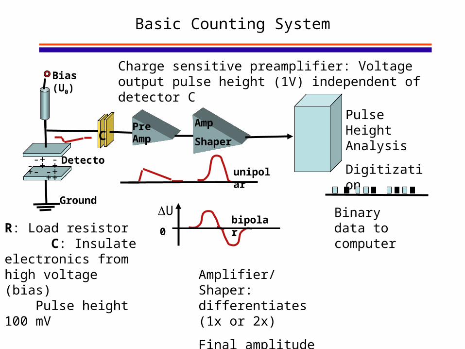
Basic Counting System
Detector
Ground
Bias (U0)
R
C
-+ - - +-+
+- -+++
Pulse Height Analysis
Digitizationunipolar
bipolar0R: Load resistor
C: Insulate electronics from high voltage (bias) Pulse height 100 mV
Charge sensitive preamplifier: Voltage output pulse height (1V) independent of detector C
Amplifier/Shaper: differentiates (1x or 2x)
Final amplitude 2-10V
Binary data to computer
PreAmp
Amp
Shaper
U
Sci
ntill
atio
nDet
W. Udo Schröder, 2004
5
Operational Amplifiers
Gain is very high (~106), inverting.Properties of amp can be determined by feedback circuit:Feeding back the negative of the input signal to the summation point cancels the signal at
Integrator
G+
--Q+Q·106
0 outinin f
in
fout in
inf
RU U
RUU
I I IR R
Rf
G+
-Rin
G+
-Rin
Cf
01outin
in ffin
out inin f
dUUI U U dtC
Cdt RI
R
G+
-Cin
Rf
inout in f
dUU C R
dt
Differentiator

Sci
ntill
atio
nDet
W. Udo Schröder, 2004
6
Charge Sensitive Preamp
Inverting, integrating preamp
Pulse decay governed by tdec1/RfCf.
Additional amplifier necessary for pulse shaping and gain.G
Cf
Rf
Cd
Rin
U
t
Sci
ntill
atio
nDet
W. Udo Schröder, 2004
7
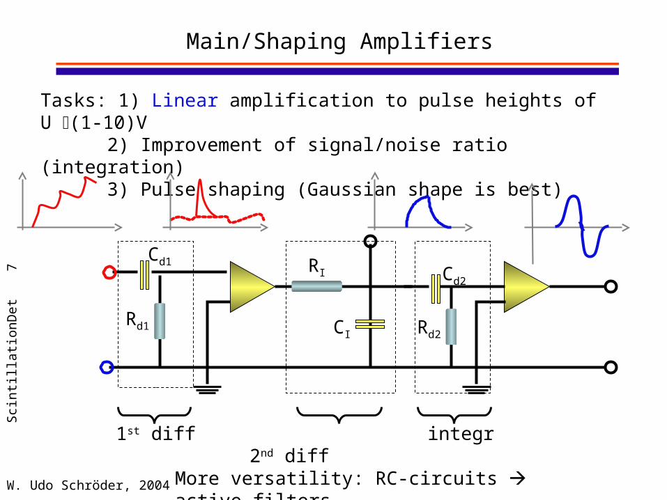
Main/Shaping Amplifiers
Tasks: 1) Linear amplification to pulse heights of U (1-10)V2) Improvement of signal/noise ratio (integration)3) Pulse shaping (Gaussian shape is best)
Cd1
Rd1
RI
CI
Cd2
Rd2
1st diff integr 2nd diff
More versatility: RC-circuits active filters
Sci
ntill
atio
nDet
W. Udo Schröder, 2004
8
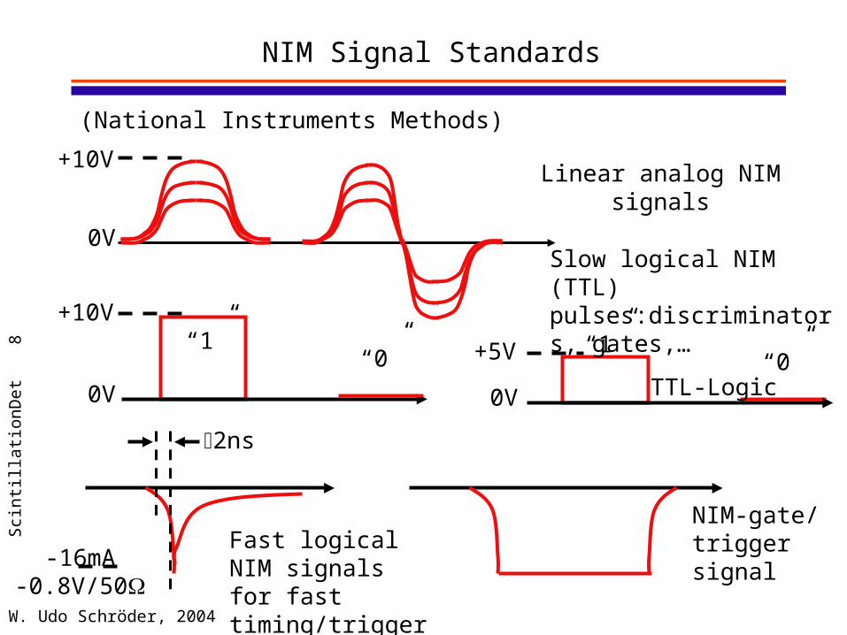
NIM Signal Standards
(National Instruments Methods)
Linear analog NIM signals+10V
0V
“1”“0”
+10V
0V
“1”+5V “0”
0V TTL-Logic
Slow logical NIM (TTL) pulses:discriminators, gates,…
-16mA-0.8V/50
2ns
Fast logical NIM signals for fast timing/triggering
NIM-gate/trigger signal

Sci
ntill
atio
nDet
W. Udo Schröder, 2004
9
Discriminator/Trigger
R1
Rf
MonoVibrator+10V
Udisc
Input Output
Task: Produce a logical signal, whenever analog signal exceeds threshold Udisc. Use for logical decisions (open acquisition,...). Exist for slow and fast pulses.
For fast timing, use negative NIM logic units
Udisc Uin
t
tUout

Sci
ntill
atio
nDet
W. Udo Schröder, 2004
10
Zero-Crossing Triggering
t
Produce fast, bipolar linear pulse. Possible: different gains for positive and negative parts zero crossing at different time (fraction of time to maximum)
Produce “saturated” uniform pulse
Differentiate saturated pulse, use triplet pulse as input for trigger (negative pulse polarity).
Trigger output appears at zero crossing
(Internal delays neglected)
t
t
Utrig
Trigger output signal t

Sci
ntill
atio
nDet
W. Udo Schröder, 2004
11
Constant-Fraction Discriminator
Uin
-1Delay
Td
Uf=f·Uin
Trigger
Zero crossing timing always at same physical time, independent of pulse amplitude for fixed pulse shape: no “walk” with energy
Ucftd
amplitude dependent leading edge discr. output timing
Can utilize for PSD!
Pulse time jitter
“walk”Udisc

Sci
ntill
atio
nDet
W. Udo Schröder, 2004
12
Logic Modules
U1
U2Uout=U
1U2
Overlap Coincidence
U2
U1
Or (inclusive)
U1
U2
Uout
t
t
t
U1
U2
Uout
t
t
t
Uout=U
1VU2
Anti-Coincidence
U
U
complementU1
U2
Uout=U1U2U2
For fast timing: use fast negative logic

Sci
ntill
atio
nDet
W. Udo Schröder, 2004
13
Signal Transmission
inner conductor
outer conductor/shield
outer conductordielectricmedium
outer casing
Coaxial cables/transmission lines traveling waves in cavity resonators
2 2
2 2
U UL C
z t
Wave equation (R=0):
z
L: inductivity/lengthC: capacity/lengthdepend on diameter and dielectric
signal propagation speed (speed of light): 1c LC typically c-1=5 ns/m
0Z L Ccharacteristic resistanceZ0=Ohmic resistance!For R≠0, Z0() complex
Z0 = 50 or 93 used for timing, spectroscopy, resp.
Sci
ntill
atio
nDet
W. Udo Schröder, 2004
14
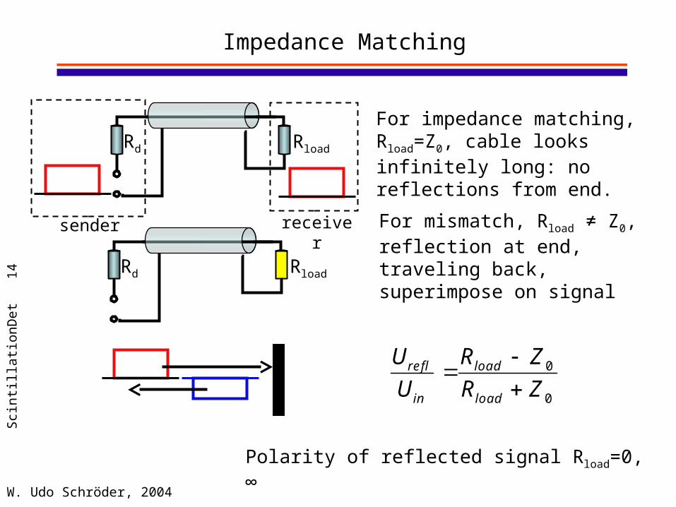
Impedance Matching
Rd Rload
Rd Rload
sender receiver
For impedance matching, Rload=Z0, cable looks infinitely long: no reflections from end.
For mismatch, Rload ≠ Z0, reflection at end, traveling back, superimpose on signal
0
0
refl load
in load
U R ZU R Z
Polarity of reflected signal Rload=0, ∞
Sci
ntill
atio
nDet
W. Udo Schröder, 2004
15
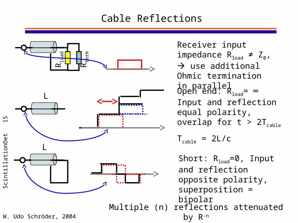
Cable Reflections
Receiver input impedance Rload ≠ Z0, use additional Ohmic termination in parallel
Rlo
ad
Rte
rm
L
L
Open end: Rload= ∞ Input and reflection equal polarity, overlap for t > 2Tcable
Tcable = 2L/c
Short: Rload=0, Input and reflection opposite polarity, superposition = bipolar
Multiple (n) reflections attenuated by R-n

Sci
ntill
atio
nDet
W. Udo Schröder, 2004
16