Embed Size (px)
Citation preview

3 Science and applications
3.1 Introduction
1 In this chapter we provide an overview of some keycurrent developments in nanoscience andnanotechnologies, and highlight some possible futureapplications. The chapter is informed by evidence fromscientists and engineers in academia and industry. Itillustrates the wide-ranging interest in these areas andprovides a background to the later chapters, whichaddress health, environmental, social, ethical andregulatory implications of nanotechnologies. It does notconsider in detail the developments in nanoscience andnanotechnologies in all scientific and engineering fields.
2 As nanoscience and nanotechnologies cover such awide range of fields (from chemistry, physics andbiology, to medicine, engineering and electronics), wehave considered them in four broad categories:nanomaterials; nanometrology; electronics,optoelectronics and information and communicationtechnology; and bio-nanotechnology andnanomedicine. This division helps to distinguishbetween developments in different fields, but there isnaturally some overlap.
3 Where possible, we define the development offuture applications as short term (under 5years),medium term (5–15 years), and long term (over20years). It may be that some of the potentialapplications that we identify are never realised, whereasothers that are currently unforeseen could have a majorimpact. We also identify potential in environmental,health and safety, ethical or societal implications oruncertainties that are discussed further in later chapters.
4 Current industrial applications of nanotechnologiesare dealt with in Chapter 4, as are the factors that willinfluence their application in the future.
3.2 Nanomaterials
3.2.1 Introduction to nanomaterials
5 A key driver in the development of new andimproved materials, from the steels of the 19th centuryto the advanced materials of today, has been the abilityto control their structure at smaller and smaller scales.The overall properties of materials as diverse as paintsand silicon chips are determined by their structure at themicro- and nanoscales. As our understanding ofmaterials at the nanoscale and our ability to controltheir structure improves, there will be great potential tocreate a range of materials with novel characteristics,functions and applications.
6 Although a broad definition, we categorisenanomaterials as those which have structuredcomponents with at least one dimension less than100nm. Materials that have one dimension in thenanoscale (and are extended in the other two dimensions)are layers, such as a thin films or surface coatings. Someof the features on computer chips come in this category.Materials that are nanoscale in two dimensions (andextended in one dimension) include nanowires andnanotubes. Materials that are nanoscale in threedimensions are particles, for example precipitates, colloidsand quantum dots (tiny particles of semiconductormaterials). Nanocrystalline materials, made up ofnanometre-sized grains, also fall into this category. Someof these materials have been available for some time;others are genuinely new. The aim of this chapter is togive an overview of the properties, and the significantforeseeable applications of some key nanomaterials.
7 Two principal factors cause the properties ofnanomaterials to differ significantly from othermaterials: increased relative surface area, and quantumeffects. These factors can change or enhance propertiessuch as reactivity, strength and electrical characteristics.As a particle decreases in size, a greater proportion ofatoms are found at the surface compared to thoseinside. For example, a particle of size 30 nm has 5% ofits atoms on its surface, at 10 nm 20% of its atoms, andat 3 nm 50% of its atoms. Thus nanoparticles have amuch greater surface area per unit mass compared withlarger particles. As growth and catalytic chemicalreactions occur at surfaces, this means that a given massof material in nanoparticulate form will be much morereactive than the same mass of material made up oflarger particles.
8 In tandem with surface-area effects, quantumeffects can begin to dominate the properties of matteras size is reduced to the nanoscale. These can affect theoptical, electrical and magnetic behaviour of materials,particularly as the structure or particle size approachesthe smaller end of the nanoscale. Materials that exploitthese effects include quantum dots, and quantum welllasers for optoelectronics.
9 For other materials such as crystalline solids, as thesize of their structural components decreases, there ismuch greater interface area within the material; this cangreatly affect both mechanical and electrical properties.For example, most metals are made up of smallcrystalline grains; the boundaries between the grainslow down or arrest the propagation of defects whenthe material is stressed, thus giving it strength. If thesegrains can be made very small, or even nanoscale insize, the interface area within the material greatly
The Royal Society & The Royal Academy of Engineering Nanoscience and nanotechnologies | July 2004 | 7
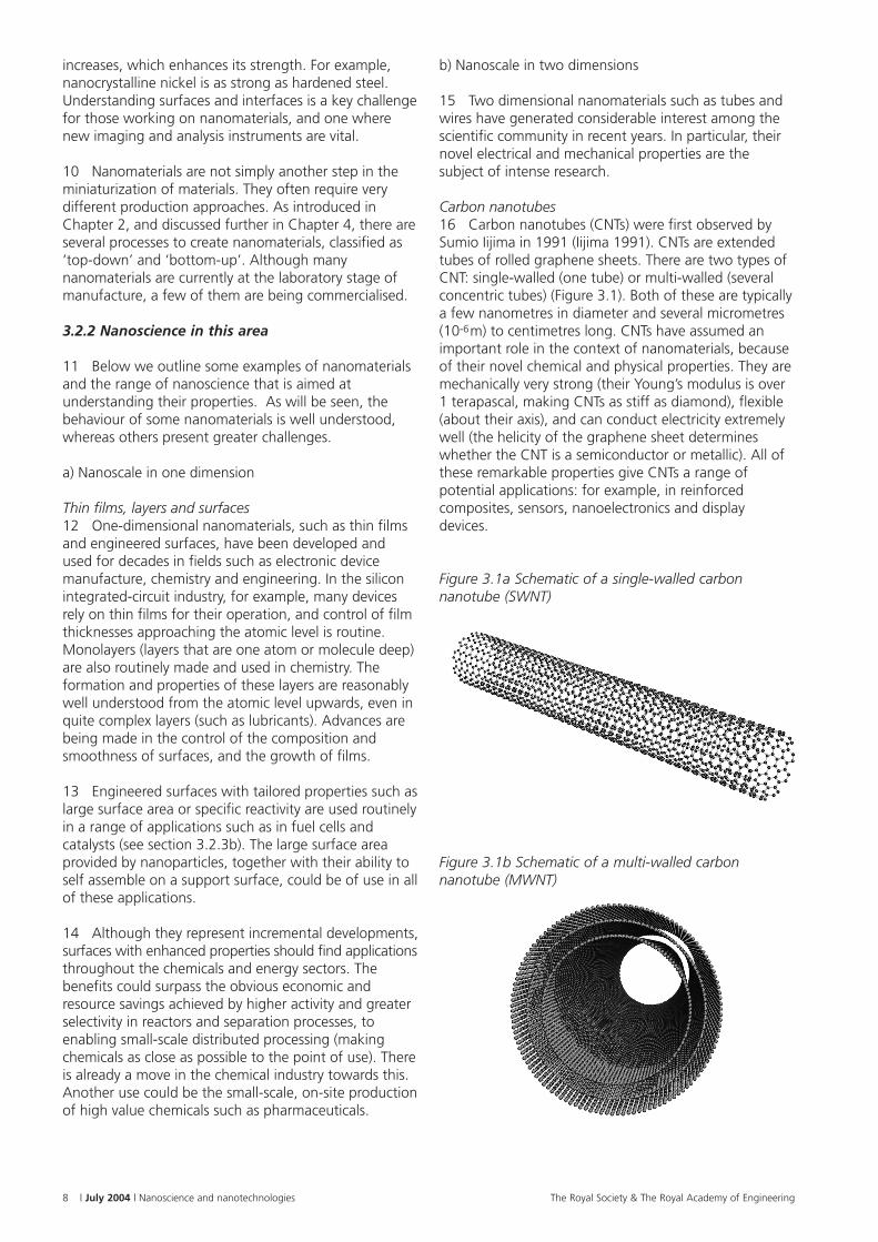
increases, which enhances its strength. For example,nanocrystalline nickel is as strong as hardened steel.Understanding surfaces and interfaces is a key challengefor those working on nanomaterials, and one wherenew imaging and analysis instruments are vital.
10 Nanomaterials are not simply another step in theminiaturization of materials. They often require verydifferent production approaches. As introduced inChapter 2, and discussed further in Chapter 4, there areseveral processes to create nanomaterials, classified as‘top-down’ and ‘bottom-up’. Although manynanomaterials are currently at the laboratory stage ofmanufacture, a few of them are being commercialised.
3.2.2 Nanoscience in this area
11 Below we outline some examples of nanomaterialsand the range of nanoscience that is aimed atunderstanding their properties. As will be seen, thebehaviour of some nanomaterials is well understood,whereas others present greater challenges.
a) Nanoscale in one dimension
Thin films, layers and surfaces12 One-dimensional nanomaterials, such as thin filmsand engineered surfaces, have been developed andused for decades in fields such as electronic devicemanufacture, chemistry and engineering. In the siliconintegrated-circuit industry, for example, many devicesrely on thin films for their operation, and control of filmthicknesses approaching the atomic level is routine.Monolayers (layers that are one atom or molecule deep)are also routinely made and used in chemistry. Theformation and properties of these layers are reasonablywell understood from the atomic level upwards, even inquite complex layers (such as lubricants). Advances arebeing made in the control of the composition andsmoothness of surfaces, and the growth of films.
13 Engineered surfaces with tailored properties such aslarge surface area or specific reactivity are used routinelyin a range of applications such as in fuel cells andcatalysts (see section 3.2.3b). The large surface areaprovided by nanoparticles, together with their ability toself assemble on a support surface, could be of use in allof these applications.
14 Although they represent incremental developments,surfaces with enhanced properties should find applicationsthroughout the chemicals and energy sectors. Thebenefits could surpass the obvious economic andresource savings achieved by higher activity and greaterselectivity in reactors and separation processes, toenabling small-scale distributed processing (makingchemicals as close as possible to the point of use). Thereis already a move in the chemical industry towards this.Another use could be the small-scale, on-site productionof high value chemicals such as pharmaceuticals.
b) Nanoscale in two dimensions
15 Two dimensional nanomaterials such as tubes andwires have generated considerable interest among thescientific community in recent years. In particular, theirnovel electrical and mechanical properties are thesubject of intense research.
Carbon nanotubes16 Carbon nanotubes (CNTs) were first observed bySumio Iijima in 1991 (Iijima 1991). CNTs are extendedtubes of rolled graphene sheets. There are two types ofCNT: single-walled (one tube) or multi-walled (severalconcentric tubes) (Figure 3.1). Both of these are typicallya few nanometres in diameter and several micrometres (10-6m) to centimetres long. CNTs have assumed animportant role in the context of nanomaterials, becauseof their novel chemical and physical properties. They aremechanically very strong (their Young’s modulus is over1 terapascal, making CNTs as stiff as diamond), flexible(about their axis), and can conduct electricity extremelywell (the helicity of the graphene sheet determineswhether the CNT is a semiconductor or metallic). All ofthese remarkable properties give CNTs a range ofpotential applications: for example, in reinforcedcomposites, sensors, nanoelectronics and displaydevices.
Figure 3.1a Schematic of a single-walled carbon nanotube (SWNT)
Figure 3.1b Schematic of a multi-walled carbon nanotube (MWNT)
The Royal Society & The Royal Academy of Engineering8 | July 2004 | Nanoscience and nanotechnologies

17 CNTs are now available commercially in limitedquantities. They can be grown by several techniques,which are discussed in section 4.3.1b. However, theselective and uniform production of CNTs with specificdimensions and physical properties is yet to be achieved.The potential similarity in size and shape between CNTsand asbestos fibres has led to concerns about their safety,which we address in detail in sections 5.3.1b and 5.3.2a.
Inorganic nanotubes18 Inorganic nanotubes and inorganic fullerene-likematerials based on layered compounds such asmolybdenum disulphide were discovered shortly afterCNTs. They have excellent tribological (lubricating)properties, resistance to shockwave impact, catalyticreactivity, and high capacity for hydrogen and lithiumstorage, which suggest a range of promisingapplications. Oxide-based nanotubes (such as titaniumdioxide) are being explored for their applications incatalysis, photo-catalysis and energy storage.
Nanowires19 Nanowires are ultrafine wires or linear arrays ofdots, formed by self-assembly. They can be made from awide range of materials. Semiconductor nanowiresmade of silicon, gallium nitride and indium phosphidehave demonstrated remarkable optical, electronic andmagnetic characteristics (for example, silica nanowirescan bend light around very tight corners). Nanowireshave potential applications in high-density data storage,either as magnetic read heads or as patterned storagemedia, and electronic and opto-electronic nanodevices,for metallic interconnects of quantum devices andnanodevices. The preparation of these nanowires relieson sophisticated growth techniques, which include self-assembly processes, where atoms arrange themselvesnaturally on stepped surfaces, chemical vapourdeposition (CVD) onto patterned substrates,electroplating or molecular beam epitaxy (MBE). The‘molecular beams’ are typically from thermallyevaporated elemental sources.
Biopolymers20 The variability and site recognition of biopolymers,such as DNA molecules, offer a wide range ofopportunities for the self-organization of wirenanostructures into much more complex patterns. TheDNA backbones may then, for example, be coated inmetal. They also offer opportunities to link nano- andbiotechnology in, for example, biocompatible sensorsand small, simple motors. Such self-assembly of organicbackbone nanostructures is often controlled by weakinteractions, such as hydrogen bonds, hydrophobic, orvan der Waals interactions (generally in aqueousenvironments) and hence requires quite differentsynthesis strategies to CNTs, for example. Thecombination of one-dimensional nanostructuresconsisting of biopolymers and inorganic compoundsopens up a number of scientific and technologicalopportunities.
c) Nanoscale in three dimensions
Nanoparticles21 Nanoparticles are often defined as particles of lessthan 100nm in diameter. In line with our definitions ofnanoscience and nanotechnologies (see Box 2.1), weclassify nanoparticles to be particles less than 100nm indiameter that exhibit new or enhanced size-dependentproperties compared with larger particles of the samematerial. Nanoparticles exist widely in the natural world:for example as the products of photochemical andvolcanic activity, and created by plants and algae. Theyhave also been created for thousands of years asproducts of combustion and food cooking, and morerecently from vehicle exhausts. Deliberatelymanufactured nanoparticles, such as metal oxides, areby comparison in the minority. In this report we willrefer to these as natural, pollutant and manufacturednanoparticles, respectively.
22 As described in Chapter 2, nanoparticles are ofinterest because of the new properties (such as chemicalreactivity and optical behaviour) that they exhibitcompared with larger particles of the same materials.For example, titanium dioxide and zinc oxide becometransparent at the nanoscale, however are able toabsorb and reflect UV light, and have found applicationin sunscreens. Nanoparticles have a range of potentialapplications: in the short-term in new cosmetics, textilesand paints; in the longer term, in methods of targeteddrug delivery where they could be to used deliver drugsto a specific site in the body. Nanoparticles can also bearranged into layers on surfaces, providing a largesurface area and hence enhanced activity, relevant to arange of potential applications such as catalysts.
23 Manufactured nanoparticles are typically notproducts in their own right, but generally serve as rawmaterials, ingredients or additives in existing products.Although their production is currently low comparedwith other nanomaterials we have given them aconsiderable amount of attention in this report. This isbecause they are currently in a small number ofconsumer products such as cosmetics and theirenhanced or novel properties may have implications fortheir toxicity. The evidence submitted during the courseof our study indicates that for most applications,nanoparticles will be fixed (for example, attached to asurface or within in a composite) although in othersthey will be free or suspended in fluid. Whether they arefixed or free will have a significant affect on theirpotential health, safety and environmental impacts. Weaddress these issues in detail in Chapter 5.
Fullerenes (carbon 60)24 In the mid-1980s a new class of carbon material wasdiscovered called carbon 60 (C60) (Kroto et al 1985). Adiagram of carbon 60 can be found in Figure 2.1. Theseare spherical molecules about 1nm in diameter,comprising 60 carbon atoms arranged as 20 hexagons
The Royal Society & The Royal Academy of Engineering Nanoscience and nanotechnologies | July 2004 | 9
and 12 pentagons: the configuration of a football. TheC60 species was named ‘Buckminsterfullerene’ inrecognition of the architect Buckminster Fuller, who waswell-known for building geodesic domes, and the termfullerenes was then given to any closed carbon cage. In1990, a technique to produce larger quantities of C60 wasdeveloped by resistively heating graphite rods in a heliumatmosphere (Krätschmer et al 1990). Several applicationsare envisaged for fullerenes, such as miniature ‘ballbearings’ to lubricate surfaces, drug delivery vehicles andin electronic circuits.
Dendrimers25 Dendrimers are spherical polymeric molecules,formed through a nanoscale hierarchical self-assemblyprocess. There are many types of dendrimer; the smallestis several nanometres in size. Dendrimers are used inconventional applications such as coatings and inks, butthey also have a range of interesting properties whichcould lead to useful applications. For example,dendrimers can act as nanoscale carrier molecules andas such could be used in drug delivery. Environmentalclean-up could be assisted by dendrimers as they cantrap metal ions, which could then be filtered out ofwater with ultra-filtration techniques.
Quantum dots26 Nanoparticles of semiconductors (quantum dots)were theorized in the 1970s and initially created in theearly 1980s. If semiconductor particles are made smallenough, quantum effects come into play, which limitthe energies at which electrons and holes (the absenceof an electron) can exist in the particles. As energy isrelated to wavelength (or colour), this means that theoptical properties of the particle can be finely tuneddepending on its size. Thus, particles can be made toemit or absorb specific wavelengths (colours) of light,merely by controlling their size. Recently, quantum dotshave found applications in composites, solar cells(Gratzel cells) and fluorescent biological labels (forexample to trace a biological molecule) which use boththe small particle size and tuneable energy levels.Recent advances in chemistry have resulted in thepreparation of monolayer-protected, high-quality,monodispersed, crystalline quantum dots as small as2nm in diameter, which can be conveniently treatedand processed as a typical chemical reagent.
3.2.3 Applications
27 Below we list some key current and potential short-and long-term applications of nanomaterials. Mostcurrent applications represent evolutionarydevelopments of existing technologies: for example, thereduction in size of electronics devices.
a) Current
Sunscreens and cosmetics28 Nanosized titanium dioxide and zinc oxide are
currently used in some sunscreens, as they absorb andreflect ultraviolet (UV) rays and yet are transparent tovisible light and so are more appealing to the consumer.Nanosized iron oxide is present in some lipsticks as apigment but it is our understanding that it is not usedby the European cosmetics sector. The use ofnanoparticles in cosmetics has raised a number ofconcerns about consumer safety; we evaluate theevidence relating to these concerns in section 5.3.2b.
Composites29 An important use of nanoparticles and nanotubesis in composites, materials that combine one or moreseparate components and which are designed to exhibitoverall the best properties of each component. Thismulti-functionality applies not only to mechanicalproperties, but extends to optical, electrical andmagnetic ones. Currently, carbon fibres and bundles ofmulti-walled CNTs are used in polymers to control orenhance conductivity, with applications such as anti-static packaging. The use of individual CNTs incomposites is a potential long-term application (seesection 3.2.3c). A particular type of nanocomposite iswhere nanoparticles act as fillers in a matrix; forexample, carbon black used as a filler to reinforce cartyres. However, particles of carbon black can range fromtens to hundreds of nanometres in size, so not allcarbon black falls within our definition of nanoparticles.
Clays30 Clays containing naturally occurring nanoparticleshave long been important as construction materials andare undergoing continuous improvement. Clay particlebased composites – containing plastics and nano-sizedflakes of clay – are also finding applications such as usein car bumpers.
Coatings and surfaces31 Coatings with thickness controlled at the nano- oratomic scale have been in routine production for sometime, for example in MBE or metal oxide CVD foroptoelectonic devices, or in catalytically active andchemically functionalized surfaces. Recently developedapplications include the self-cleaning window, which iscoated in highly activated titanium dioxide, engineeredto be highly hydrophobic (water repellent) and anti-bacterial, and coatings based on nanoparticulate oxidesthat catalytically destroy chemical agents (Royal Society2004a). Wear and scratch-resistant hard coatings aresignificantly improved by nanoscale intermediate layers (ormultilayers) between the hard outer layer and thesubstrate material. The intermediate layers give goodbonding and graded matching of elastic and thermalproperties, thus improving adhesion. A range of enhancedtextiles, such as breathable, waterproof and stain-resistant fabrics, have been enabled by the improvedcontrol of porosity at the nanoscale and surfaceroughness in a variety of polymers and inorganics.
The Royal Society & The Royal Academy of Engineering10 | July 2004 | Nanoscience and nanotechnologies
Tougher and harder cutting tools32 Cutting tools made of nanocrystalline materials,such as tungsten carbide, tantalum carbide and titaniumcarbide, are more wear and erosion-resistant, and lastlonger than their conventional (large-grained)counterparts. They are finding applications in the drillsused to bore holes in circuit boards.
b) Short-term
Paints33 Incorporating nanoparticles in paints could improvetheir performance, for example by making them lighterand giving them different properties. Thinner paintcoatings (‘lightweighting’), used for example on aircraft,would reduce their weight, which could be beneficial tothe environment. However, the whole life cycle of theaircraft needs to be considered before overall benefitscan be claimed (see section 4.5). It may also be possibleto substantially reduce solvent content of paints, withresulting environmental benefits. New types of fouling-resistant marine paint could be developed and areurgently needed as alternatives to tributyl tin (TBT), nowthat the ecological impacts of TBT have beenrecognised. Anti-fouling surface treatment is alsovaluable in process applications such as heat exchange,where it could lead to energy savings. If they can beproduced at sufficiently low cost, fouling-resistantcoatings could be used in routine duties such as pipingfor domestic and industrial water systems. It remainsspeculation whether very effective anti-fouling coatingscould reduce the use of biocides, including chlorine.Other novel, and more long-term, applications fornanoparticles might lie in paints that change colour inresponse to change in temperature or chemicalenvironment, or paints that have reduced infra-redabsorptivity and so reduce heat loss.
34 Concerns about the health and environmentalimpacts of nanoparticles (which we address in detail inChapter 5) may require the need for the durability andabrasion behaviour of nano-engineered paints andcoatings to be addressed, so that abrasion products takethe form of coarse or microscopic agglomerates ratherthan individual nanoparticles.
Remediation35 The potential of nanoparticles to react withpollutants in soil and groundwater and transform theminto harmless compounds is being researched. In onepilot study the large surface area and high surfacereactivity of iron nanoparticles were exploited totransform chlorinated hydrocarbons (some of which arebelieved to be carcinogens) into less harmful endproducts in groundwater (Zhang 2003). It is also hopedthat they could be used to transform heavy metals suchas lead and mercury from bioavailable forms intoinsoluble forms. Serious concerns have been raised overthe uncontrolled release of nanoparticles into theenvironment; these are discussed in section 5.4.
Fuel Cells36 Engineered surfaces are essential in fuel cells, wherethe external surface properties and the pore structureaffect performance. The hydrogen used as the immediatefuel in fuel cells may be generated from hydrocarbonsby catalytic reforming, usually in a reactor moduleassociated directly with the fuel cell. The potential useof nano-engineered membranes to intensify catalyticprocesses could enable higher-efficiency, small-scale fuelcells. These could act as distributed sources of electricalpower. It may eventually be possible to producehydrogen locally from sources other than hydrocarbons,which are the feedstocks of current attention.
Displays37 The huge market for large area, high brightness,flat-panel displays, as used in television screens andcomputer monitors, is driving the development of somenanomaterials. Nanocrystalline zinc selenide, zincsulphide, cadmium sulphide and lead telluridesynthesized by sol–gel techniques (a process for makingceramic and glass materials, involving the transitionfrom a liquid ‘sol’ phase to a solid ‘gel’ phase) arecandidates for the next generation of light-emittingphosphors. CNTs are being investigated for low voltagefield-emission displays; their strength, sharpness,conductivity and inertness make them potentially veryefficient and long-lasting emitters.
Batteries38 With the growth in portable electronic equipment(mobile phones, navigation devices, laptop computers,remote sensors), there is great demand for lightweight,high-energy density batteries. Nanocrystalline materialssynthesized by sol–gel techniques are candidates forseparator plates in batteries because of their foam-like(aerogel) structure, which can hold considerably moreenergy than conventional ones. Nickel–metal hydridebatteries made of nanocrystalline nickel and metalhydrides are envisioned to require less frequentrecharging and to last longer because of their largegrain boundary (surface) area.
Fuel additives39 Research is underway into the addition ofnanoparticulate ceria (cerium oxide) to diesel fuel toimprove fuel economy by reducing the degradation offuel consumption over time (Oxonica 2003).
Catalysts40 In general, nanoparticles have a high surface area,and hence provide higher catalytic activity.Nanotechnologies are enabling changes in the degree ofcontrol in the production of nanoparticles, and thesupport structure on which they reside. It is possible tosynthesise metal nanoparticles in solution in thepresence of a surfactant to form highly orderedmonodisperse films of the catalyst nanoparticles on asurface. This allows more uniformity in the size andchemical structure of the catalyst, which in turn leads to
The Royal Society & The Royal Academy of Engineering Nanoscience and nanotechnologies | July 2004 | 11

greater catalytic activity and the production of fewer by-products. It may also be possible to engineer specific orselective activity. These more active and durablecatalysts could find early application in cleaning upwaste streams. This will be particularly beneficial if itreduces the demand for platinum-group metals, whoseuse in standard catalytic units is starting to emerge as aproblem, given the limited availability of these metals.
c) Longer-term applications
Carbon nanotube composites41 CNTs have exceptional mechanical properties,particularly high tensile strength and light weight. Anobvious area of application would be in nanotube-reinforced composites, with performance beyondcurrent carbon-fibre composites. One current limit tothe introduction of CNTs in composites is the problem ofstructuring the tangle of nanotubes in a well-orderedmanner so that use can be made of their strength.Another challenge is generating strong bondingbetween CNTs and the matrix, to give good overallcomposite performance and retention during wear orerosion of composites. The surfaces of CNTs are smoothand relatively unreactive, and so tend to slip through thematrix when it is stressed. One approach that is beingexplored to prevent this slippage is the attachment ofchemical side-groups to CNTs, effectively to form‘anchors’. Another limiting factor is the cost ofproduction of CNTs. However, the potential benefits ofsuch light, high strength material in numerousapplications for transportation are such that significantfurther research is likely.
Lubricants42 Nanospheres of inorganic materials could be usedas lubricants, in essence by acting as nanosized ‘ballbearings’. The controlled shape is claimed to make themmore durable than conventional solid lubricants andwear additives. Whether the increased financial andresource cost of producing them is offset by the longerservice life of lubricants and parts remains to beinvestigated (along the lines of the methodologyoutlined in section 4.5). It is also claimed that thesenanoparticles reduce friction between metal surfaces,particularly at high normal loads. If so, they should findtheir first applications in high-performance engines anddrivers; this could include the energy sector as well astransport. There is a further claim that this type oflubricant is effective even if the metal surfaces are nothighly smooth. Again, the benefits of reduced cost andresource input for machining must be compared againstproduction of nanolubricants. In all these applications,the particles would be dispersed in a conventional liquidlubricant; design of the lubricant system must thereforeinclude measures to contain and manage waste.
Magnetic materials43 It has been shown that magnets made ofnanocrystalline yttrium–samarium–cobalt grains possess
unusual magnetic properties due to their extremelylarge grain interface area (high coercivity can beobtained because magnetization flips cannot easilypropagate past the grain boundaries). This could lead toapplications in motors, analytical instruments likemagnetic resonance imaging (MRI), used widely inhospitals, and microsensors. Overall magnetisation,however, is currently limited by the ability to align thegrains’ direction of magnetisation.
44 Nanoscale-fabricated magnetic materials also haveapplications in data storage. Devices such as computerhard disks depend on the ability to magnetize smallareas of a spinning disk to record information. If thearea required to record one piece of information can beshrunk in the nanoscale (and can be written and readreliably), the storage capacity of the disk can beimproved dramatically. In the future, the devices oncomputer chips which currently operate using flows ofelectrons could use the magnetic properties of theseelectrons, called spin, with numerous advantages.Recent advances in novel magnetic materials and theirnanofabrication are encouraging in this respect.
Medical implants45 Current medical implants, such as orthopaedicimplants and heart valves, are made of titanium andstainless steel alloys, primarily because they are bio-compatible. Unfortunately, in some cases these metalalloys may wear out within the lifetime of the patient.Nanocrystalline zirconium oxide (zirconia) is hard, wear-resistant, bio-corrosion resistant and bio-compatible. Ittherefore presents an attractive alternative material forimplants. It and other nanoceramics can also be madeas strong, light aerogels by sol–gel techniques.Nanocrystalline silicon carbide is a candidate material forartificial heart valves primarily because of its low weight,high strength and inertness.
Machinable ceramics46 Ceramics are hard, brittle and difficult to machine.However, with a reduction in grain size to thenanoscale, ceramic ductility can be increased. Zirconia,normally a hard, brittle ceramic, has even been renderedsuperplastic (for example, able to be deformed up to300% of its original length). Nanocrystalline ceramics,such as silicon nitride and silicon carbide, have beenused in such automotive applications as high-strengthsprings, ball bearings and valve lifters, because they canbe easily formed and machined, as well as exhibitingexcellent chemical and high-temperature properties.They are also used as components in high-temperaturefurnaces. Nanocrystalline ceramics can be pressed intocomplex net shapes and sintered at significantly lowertemperatures than conventional ceramics.
Water purification47 Nano-engineered membranes could potentially leadto more energy-efficient water purification processes,notably in desalination by reverse osmosis. Again, these
The Royal Society & The Royal Academy of Engineering12 | July 2004 | Nanoscience and nanotechnologies

applications would represent incremental improvementsin technologies that are already available. They woulduse fixed nanoparticles, and are therefore distinct fromapplications that propose to use free nanoparticles.
Military battle suits48 Enhanced nanomaterials form the basis of a state-of-the-art ‘battle suit’ that is being developed by theInstitute of Soldier Nanotechnologies at MassachusettsInstitute of Technology, USA (MIT 2004). A short-termdevelopment is likely to be energy-absorbing materialsthat will withstand blast waves; longer-term are thosethat incorporate sensors to detect or respond tochemical and biological weapons (for example,responsive nanopores that ‘close’ upon detection of abiological agent). There is speculation thatdevelopments could include materials which monitorphysiology while a soldier is still on the battlefield, anduniforms with potential medical applications, such assplints for broken bones. In section 6.7 we consider thepossible social implications of the exploitation ofnanotechnologies for military purposes.
3.3 Nanometrology
3.3.1 Introduction to nanometrology
49 The science of measurement at the nanoscale iscalled nanometrology. Its application underpins all ofnanoscience and nanotechnologies. The ability tomeasure and characterise materials (determine theirsize, shape and physical properties) at the nanoscale isvital if nanomaterials and devices are to be produced toa high degree of accuracy and reliability and theapplications of nanotechnologies are to be realised.Nanometrology includes length or size measurements(where dimensions are typically given in nanometres andthe measurement uncertainty is often less than 1nm) aswell as measurement of force, mass, electrical and otherproperties. As techniques for making thesemeasurements advance, so too does the understandingof nanoscale behaviour and therefore the possibility ofimproving materials, industrial processes and reliabilityof manufacture. The instruments for making suchmeasurements are many and varied; a description ofsome key instruments is given in Box 3.1. Thecharacterisation of materials, particularly in theindustrial context, is discussed further in Chapter 4.
50 As with all measurement, nanometrology isessentially an enabling technology. Nanotechnologies,however defined, cannot progress independently ofprogress in nanometrology. Apart from their directinfluence on scientific research and its application, thesolutions developed for nanometrology problems canoften be exploited elsewhere. For example, the conceptof the AFM, a key nanometrology tool, has had a directinfluence on lithographic processes and techniques formolecular manipulation. Conversely, it is likely that
continuing research into nanodevices will suggest newmeasurement methods.
51 Making measurements with nanoscale precisionposes several major difficulties. Environmentalfluctuations such as vibration or temperature changehave a large effect at the nanoscale. For example, anyexternal change to the large machines used inmanufacturing microelectronics components will affectthe creation of nanoscale features and their cruciallyimportant alignment to each other. The ability tomeasure these influences, and thereafter to minimisethem, is therefore vital.
52 Currently, instruments are available that can makesufficiently precise measurements to support laboratoryresearch. There are a number of sensor technologiesand instruments with nanometre, or better, sensitivityfor measuring length that repeat well if used carefully,including the scanning probe and electron microscopesand some optical devices (see Box 3.1). However,universal measurement standards have not yet beenestablished. Data published recently from thePhysikalisch-Technische Bundesanstalt in Germany (Breilet al 2002) shows that even apparently sophisticatedusers of atomic force microscopes can produce largevariations in their measurements of the same artefacts.Without agreed standards, tools or machines cannot becalibrated at the nanometre scale. It is therefore not yetpossible for laboratories and manufacturing plants toexchange or compare data or physical components.Also, health and safety standards cannot be set for legalrequirements. Nanoparticle characterization for size, sizedistribution and shape is also lacking formal methods.
53 Evidence presented at our industry workshophighlighted that good comparative metrology is provingdifficult to develop. There is no particular difficulty withworking at the nanoscale within a single laboratory ororganization in the sense artifacts (either universal or in-house ‘gold standards’ such as the spacing of the siliconlattice) can be used to calibrate instruments so thatthere is self-consistency across a set of measurements.In doing this there must naturally be levels of protectionagainst vibration, thermal changes, etc that arebecoming increasingly stringent. However, thedetermination of absolute measurements of length atthe nanometer scale and below is very difficult andexpensive.
3.3.2 Length measurement
54 Although there is not currently an internationalstandard that can be applied to them, calibrationartefacts are becoming available for AFMs for lengthmeasurement calibration in each of the threedimensions. Such artefacts can also be used for tipcharacterization, as the exact shape of the fine tipwhich scans across the surface can strongly influencelength measurements, particularly when the tip
The Royal Society & The Royal Academy of Engineering Nanoscience and nanotechnologies | July 2004 | 13

becomes blunt. The National Physical Laboratory (NPL)in the UK has a considerable reputation in formalmetrology and has done much to develop measurementcapability as well as to take responsibility for the UK’snational standards. It also has excellent realisations ofthe metre, mainly through optical and x-rayinterferometry, that can calibrate transfer standards withuncertainties of the order of nanometres when workingwith sufficiently large wave-fronts. However,comparative methods (akin to the interferometricmeasurement of optical lenses and mirrors) becomeineffective when working with very small objectscomparable to the wavelength of the photons beingused. Hence, it is not yet possible to accuratelydetermine dimensions or shape in all axes. Manysurface characterization methods (especially for theelectronics industries) directly exploit comparison via x-ray (occasionally optical) reflection or diffraction. It islikely that the practice of length metrology would beimproved through better, more easily-used calibrationsystems and improved instrument design, relative to thecurrent commercial versions. Undoubtedly, bettereducation in best practice for nanometrology would alsopartly address this issue.
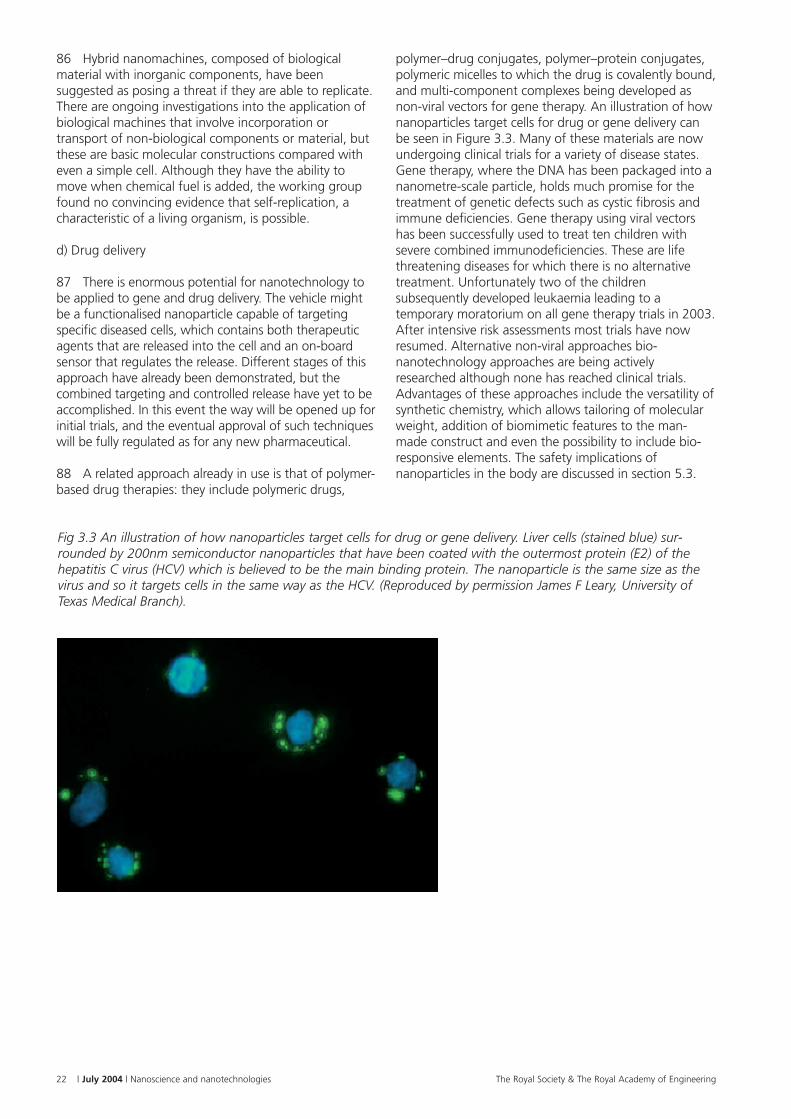
3.3.3 Force measurement
55 Along with length measurement, forcemeasurement (measured in Newtons (N)) is likely tobecome an important area of nanometrology. Thecontrol of probe stiffness and geometry will need toimprove if truly quantitative measurements of surfacemechanical properties can be made, particularly whenmeasuring biological and other soft materials. There isalso likely to be an increasing need to accuratelymeasure the elasticity of protein and nucleotidemolecules, to determine bond strength and otherproperties of the molecules. Currently, there is a largecapability gap in this field. There is a large, and growing,need for force characterisation in the pico- tomicronewton (10–12–10–6N) range. Currently, no fullysatisfactory techniques are available either for secondarystandards or transfer artefacts, although a few researchprojects are in progress (NPL and the National Institutefor Standards and Technology (NIST), USA, are bothlooking at methods based on electrostatic forces).Several groups, mainly within or sponsored by nationallaboratories (such as NPL and Warwick University in theUK, and NIST in the USA), are investigating systems thatrelate force to electrical properties and so to quantumstandards. However, so far all of them remainexperimental and a great deal more work is urgentlyneeded into fundamental and transfer standards forforces much smaller than millinewtons. Unlike lengthmeasurement, there is also a lack of readily availableand applicable force or mass instrumentation withsensitivity adequate for engineering on the nanometrescale. AFM cantilevers have nanonewton forcesensitivity, but their calibration tends to be throughindirect calculation from their dimensions, and batch-to-
batch repeatability may be poor. Some nano-indentationinstruments for hardness measurement use micro-electromechanical systems (MEMS), with broadly similarquestions over traceability. Thus there is urgent need forresearch into basic laboratory and industrial nanoforceinstrumentation alongside that for standards.
3.3.4 Measurement of single molecules
56 In the longer term, development in measurement atthe scale of the single molecule is expected.Measurements of single organic molecules and ofstructures such as single-wall nanotubes are alreadymade, providing the molecules can be anchored to asubstrate. Electron microscope and AFM/STMdeterminations of shape are relatively routine in manyresearch laboratories. Increasingly, there is interest inmolecule stiffness, in effect producing a tensile testcurve in which jumps indicate the breaking and byinference the location of various types of bond in foldedproteins and nucleotides. AFM manufacturers arestarting to offer options that can do this without theneed for the skills of a large research team.
3.3.5 Applications
57 Metrology forms the basis of the semiconductorindustry and as such is enormously advanced. TheInternational Technology Roadmap for Semiconductors(ITRS) roadmap (see also section 3.4) highlights a seriesof challenges for nanometrology if it is to keep pacewith the reduction in feature size of semiconductordevices. Shrinking feature sizes, tighter control of deviceelectrical parameters and new interconnect materialswill provide the main challenges for physical metrologymethods. To achieve desired device scaling, metrologytools must be capable of measurement of properties atatomic distances. Compounding these is the uncertainnature of the development of device design, making itdifficult to predict metrology needs in the long term andin particular the necessary metrology for manufacturingto ensure reliability. A major need is to integratemetrology data into the manufacturing process.
58 The developing capabilities of semiconductorprocessing, particularly the ever-reducing dimensionsthat can be defined using lithographic tools, are beingcombined with the techniques developed for MEMSdevice fabrication to enable the manufacture of electro-mechanical components with sub-100nmdimensions. The exploitation of these structures innano-electromechanical systems (NEMS) devices hasproduced some interesting and exciting developments inthe field of nanometrology. For example, Schwab et al(2000) have made a NEMS device that has enabled themeasurement of the quantum of thermal conductance.
59 Another group has made ultra-thin siliconcantilevers with attonewton (10–18N) sensitivity. Thesedevices have potential applications in the
The Royal Society & The Royal Academy of Engineering14 | July 2004 | Nanoscience and nanotechnologies

characterisation of single molecule properties and areexamples of how the field of NEMS is increasing thecapabilities of nanometrology.
60 The role of nanometrology and in particular theneed for the standardisation of measurement at thenanometre scale is explored further in section 8.4.3.There is a need to develop agreed standards that can beused to calibrate equipment that will be used by bothindustry and regulators. We believe that this can best beaddressed through existing programmes such as theDepartment of Trade and Industry (DTI) NationalMeasurement System Programme and should beundertaken in collaboration with industry.
We recommend that the DTI supports thestandardisation of measurement at the nanometrescale required by regulators and for quality controlin industry through the adequate funding ofinitiatives under its National Measurement SystemProgramme, and that it ensures that the UK is inthe forefront of any international initiatives forthe standardisation of measurement.
61 We are pleased to learn that initial steps in this areaare being undertaken by the British StandardsInstitution, as part of the European Committee forStandardisation Technical Board working group onnanotechnology.
The Royal Society & The Royal Academy of Engineering Nanoscience and nanotechnologies | July 2004 | 15
The Royal Society & The Royal Academy of Engineering16 | July 2004 | Nanoscience and nanotechnologies
Box 3.1 Instruments used in nanometrology
a) Electron beam techniquesTransmission electron microscopy (TEM) is used to investigate the internal structure of micro- and nanostructures.It works by passing electrons through the sample and using magnetic lenses to focus the image of the structure,much like light is transmitted through materials in conventional light microscopes. Because the wavelength of theelectrons is much shorter than that of light, much higher spatial resolution is attainable for TEM images than fora light microscope. TEM can reveal the finest details of internal structure, in some cases individual atoms. Thesamples used for TEM must be very thin (usually less than 100nm), so that many electrons can be transmittedacross the specimen. However, some materials, such as nanotubes, nanocrystalline powders or small clusters, canbe directly analysed by deposition on a TEM grid with a carbon support film. TEM and high-resolutiontransmission electron microscopy (HRTEM) are among the most important tools used to image the internalstructure of a sample. Furthermore, if the HRTEM is adequately equipped, chemical analysis can be performed byexploiting the interactions of the electrons with the atoms in the sample.
The scanning electron microscope (SEM) uses many of the basic technology developed for the TEM to provideimages of surface features associated with a sample. Here, a beam of electrons is focused to a diameter spot ofapproximately 1nm in diameter on the surface of the specimen and scanned back and forth across the surface.The surface topography of a specimen is revealed either by the reflected (backscattered) electrons generated orby electrons ejected from the specimen as the incident electrons decelerate secondary electrons. A visual image,corresponding to the signal produced by the interaction between the beam spot and the specimen at each pointalong each scan line, is simultaneously built up on the face of a cathode ray tube similar to the way that atelevision picture is generated. The best spatial resolution currently achieved is of the order of 1nm.
b) Scanning probe techniquesScanning probe microscopy (SPM) uses the interaction between a sharp tip and a surface to obtain an image. Thesharp tip is held very close to the surface to be examined and is scanned back-and-forth. The scanning tunnellingmicroscope (STM) was invented in 1981 by Gerd Binnig and Heinrich Rohrer, who went on to collect the NobelPrize for Physics in 1986. Here, a sharp conducting tip is held sufficiently close to a surface (typically about0.5nm) that electrons can ‘tunnel’ across the gap. The method provides surface structural and electronicinformation with atomic resolution. The invention of the STM led directly to the development of other ‘scanningprobe’ microscopes, such as the atomic force microscope. The atomic force microscope (AFM) uses a sharp tip onthe end of a flexible beam or cantilever. As the tip is scanned across the sample, the displacement of the end ofthe cantilever is measured, usually a laser beam. Unlike the STM, where the sample has to be conductive, an AFMcan image insulating materials simply because the signal corresponds to the force between the tip and sample,which reflects the topography being scanned across.
There are several different modes for AFM. In contact mode, the tip touches the sample; this is simple toimplement but can lead to sample damage from the dragging tip on soft materials. Tapping mode mitigates thisdifficulty: the tip is oscillated and only touches intermittently, so that dragging during scanning is minimized.Non-contact mode is where the tip senses only the attractive forces with the surface, and causes no damage. It istechnically more difficult to implement since these forces are weak compared with contact forces. In non-contactmode at larger tip-surface separation, the imaging resolution is poor, and the technique not often used.However, at small separation, which requires specialized AFM apparatus to maintain, true atomic resolution canbe achieved in non-contact mode AFM.
c) Optical tweezers (single beam gradient trap)Optical tweezers use a single laser beam (focused by a high-quality microscope objective) to a spot on a specimenplane. The radiation pressure and gradient forces from the spot creates an ‘optical trap’ which is able to hold aparticle at its centre. Small interatomic forces and displacements can then be measured. Samples that cananalysed range from single atoms and micrometre-sized spheres to strands of DNA and living cells. Opticaltweezers are now a standard method of manipulation and measurement. Numerous traps can be usedsimultaneously with other optical techniques, such as laser scalpels, which can cut the particle being studied.

3.4 Electronics, optoelectronics and informa-tion and communication technology (ICT)
3.4.1 Introduction to electronics, optoelectronics and ICT
62 The past 30 years has seen a revolution ininformation technology (IT) that has impacted the livesof many people around the world. At the heart of thisrevolution is the desire to share information, whetherthe printed word, images or sounds. This requires atechnology that can absorb and process information onone side of the planet and deliver it almostinstantaneously to the other in a form that is immediatelyaccessible. Such a technology places enormous pressureon advances in processing and storing information, andon transmitting it and converting it from and to a humanreadable form. It also increasingly requires secureencryption of information so that access to informationcan ultimately be restricted to particular individuals.
63 The market size of the IT industry is currently around$1000 billion, the order of $150 for every human beingon the planet, with an expectation that it will reach$3000 billion in 2020. In no other industry sector is thetrend for miniaturisation so apparent. This is perhapsmost obvious by charting the number of transistors, thebuilding blocks of computer chips, over the past30years. In 1971 there were just 2300 transistors onIntel’s 4004, their first computer chip, with a clockspeed (a measure of how fast the chip could operate) of0.8 million cycles per second. By 2003 the Intel Xeonprocessor had 108 million transistors operating at clockspeeds in excess of 3,000 million cycles per second.Remarkably, the physical size of the computer chip hasremained virtually unchanged over this time; it is thetransistor and all the circuitry associated with it that hasshrunk dramatically. The increase in the number oftransistors on a chip coupled with increased speed havefuelled the economics of the IT industry; in 1971 thefabrication of a single transistor cost about 10 cents; itis currently less than one-thousandth of a cent. Thisevolutionary progression of technology is charted andanticipated in the ITRS roadmap, a worldwideconsensus-based document that predicts the maintrends in the semiconductor industry 15 years into thefuture (ITRS 2003) The roadmap which defines in detailall elements of technology that have to be realised foreach step change improvement in manufacturingprocess. This roadmap is used by all industries that aredirectly or indirectly involved in the manufacture ofsilicon chips. It identifies material, architecture,metrology and process challenges as well as addressingenvironmental and heath issues in manufacturing.
3.4.2 Nanoscience in this area
64 Nanoscience research in ICT shares many of the samegoals as for other applications of nanotechnologies: animproved understanding of nanoscale properties of
materials and devices, advances in fabrication andprocess technology to satisfy increasingly stringentdimensional tolerances, and exploration of alternativetechnologies that may offer economic or performancebenefit. There is no doubt that the ICT sector haseffectively driven a large proportion of nanoscience.Indeed, the first use of the word nanotechnology was inrelation to ultra thin layers of relevance to the then up-and-coming semiconductor industry. Since then, theresearch into all aspects of semiconductor devicefabrication, from fundamental physics to processtechnology, has dominated the nanoscience landscapeand will continue so to do. Decreasing device scales willadd further impetus to the truly nanoscalar aspects ofthis global research activity. The ICT sector is, and forhistorical and economic reasons is likely to remain,heavily silicon-based for the foreseeable future.However, the end of the ITRS roadmap, currently set at2018 (commonly referred to as the end of Moore’s Law)has prompted intensive research into alternative orhybrid technologies for electronics such as conductingpolymers, which are discussed further below.
3.4.3 Current applications
Computer chips65 The dominant role of miniaturisation in the evolutionof the computer chip is reflected in the fact that the ITRSroadmap defines a manufacturing process standard – atechnology node – in terms of a length. The current130 nm technology node that produces the Intel Xeonprocessor defines the size of the DRAM (dynamicrandom access memory) half-pitch (half the distancebetween two adjacent metal wires in a memory cell).This is turn places a requirement on the lithography,process technology and metrology required tomanufacture a working device to this tolerance. As acomparison, the 1971 Intel 4004 chip used 10,000 nmtechnology; the chips of 2007 and 2013 will require65nm and 32nm technology, respectively. In the broadestsense, computer chips in current manufacture aretherefore already using nanotechnologies and havebeen so doing for over 20years. Furthermore, it is notsimply the DRAM half-pitch that is on the nanometrescale. All the technology that goes into the research,metrology and production of chips has been working, insome cases, at the sub-nanometre atomic level. Thevariety of tools that support the IT industry includescomputer modelling of advanced devices and materialsatom by atom, microscopies that can image single atoms,metrologies that can define the absolute position of asingle atomic defect over a 30cm diameter wafer (thesubstrate used for computer chips), thin-film growthprocesses that can produce layers of material with atomicprecision, and lithographies that can ‘write’ features,such as the DRAM cell, with an accuracy of sub-10nm.
Information storage66. A technology that has necessarily developed intandem with IT is that of memory for data storage. This
The Royal Society & The Royal Academy of Engineering Nanoscience and nanotechnologies | July 2004 | 17

can be divided into two quite different types: solid-statememory such as DRAM that a processor chip would useor flash memory for storing images in a digital camera;and disk-based memory such as the magnetic harddrives as found in all computers. Solid-state memoryessentially uses the same processes and technology asthe computer chip, with very similar design rules and asimilar emphasis on packing more memory into a givenarea to increase total memory per device. Thedevelopment of the hard disk drive, however, has takena quite different route in evolution as it is based onreading and writing information magnetically to aspinning disk. It is therefore primarily mechanical, ormore strictly electro-mechanical, and presents quitedifferent technical challenges. Once again, however, theimportance of length scales is paramount as the idealdisk drive is one that has the minimal physical size witha massive ability to store data. This is reflected in theevolution of the disk drive over the past 50years. Thefirst magnetic hard drive was developed by IBM in 1956and required fifty 24 inch disks to store five megabytes(million bytes) of data. In 1999 IBM introduced a73gigabyte (thousand million bytes) drive that could fitinside a personal computer; that is, over 14,000 timesthe available data storage in a device less than one-thousandth the size of the 1956 drive. Although theindividual bits of magnetic information that are writtenonto the disk drive to give it the high-density storageare currently smaller than 100nm, the constraintsrelated to this nanotechnology on other aspects of thedrive require fabrication of components with evengreater precision. The importance of thisnanotechnology in the related compact disk (CD) anddigital versatile disk (DVD) drives that are nowcommonplace is equally ubiquitous.
Optoelectronics67 The other crucial element of the IT revolution,optoelectronics, relates to devices that rely onconverting electrical signals to and from light for datatransmission, for displays for optical-based sensing and,in the future, for optical-based computing. Technologyin this sector is strongly associated with those describedabove, and relies substantially on the tools developedthere. Although some optoelectronic devices do notdepend so critically on miniaturisation as computerchips do, there is nevertheless a similar trend towardsminiaturisation, with some existing components, such asquantum-well lasers and liquid crystal displays, requiringnanometre precision in their fabrication.
3.4.4 Applications anticipated in the future
68 The future development of hardware for the ITindustry can be conveniently separated into two paths:a path that is following the well-established ITRSroadmap (which projects out to 2018); and a path thatexplores alternative technologies and materials that maysupersede the roadmap.
69 For the roadmap, miniaturisation remains a keydriving force, so that a 22nm technology node isenvisaged for manufacture in 2016. Having set thistechnology target, it is possible to anticipate all thechallenges associated with realising it. Such challengesare detailed extensively in the roadmap but includeenhancing performance by introducing new materialssuch as low dielectrics and higher-conductivityinterconnects (wiring), developing lithographies capableof fabricating structures in the sub-50nm range, andintegrating advanced metrology tools into themanufacturing process capable of detecting and sizingdefects down to the nanometre size. As such,nanoscience and nanotechnologies will continue tohave a pivotal role in developing new generations ofchips. Related technology such as flash memory willevolve in a similar fashion, with the aim of maximisingmemory capacity in the smallest possible device.
70 Hard disk technologies, although not explicitly partof the ITRS roadmap, will continue to increase in memorydensity. However, there are prospects for some stepchanges in technology that may significantly change thedata storage industry. One obvious potential trend is forsolid-state memory to replace disk-based memory. Thisis already obvious in, for example, personal musicplayers where, as solid-state memory increases indensity, hard-disk-based storage is competing with thejog-proof solid-state players. It is likely that the harddisk, whether magnetic or optical, will still be the choicefor large volume data storage for the foreseeable future,especially as the bit size shrinks even further. This is anactive area of nanoscience research.
71 Optoelectronics, although not as dependent uponlength-scale tolerances as computer chips and datastorage, will nevertheless have challenges of its own.Integration of optical components into silicon deviceshas started and can be expected to evolve further. Someof the challenges where nanotechnologies will have animpact will be in the area of photonic band-gapmaterials, where the propagation of light through adevice can be controlled with the aim of computingwith light. Photonic crystals, fabricated either through alithographic process or through a self-assemblytechnique, confine light into precisely controlledpathways in a device structure so that both transmissionand functionality can be combined into a singlestructure. A typical photonic crystal would consist of anarray of holes in a dielectric material, fabricated withsub-10nm accuracy, so that the periodicity of the holesdetermines the ability of the material to transmit thelight at any given wavelength. The development ofphotonic crystals could mean that optical integratedcircuits are shrunk further, making a significant impactin areas such as communications and optical computing.
72 Quantum computing and quantum cryptographywill also benefit from advances in optoelectronics. Bothtechnologies rely on the fact that discrete energy
The Royal Society & The Royal Academy of Engineering18 | July 2004 | Nanoscience and nanotechnologies

(quantum) levels increasingly dominate as electromagneticenergy is confined into smaller and smaller structures.Assuming that the considerable technological challengesof making nanostructures from complex materials canbe solved, in some cases by designing at the level of thesingle atom, then on a 10year time-scale quantumcryptography (a much more secure encryptiontechnology) will replace current encryption methods. Ona similar time-scale, quantum computing will start toprovide solutions to complex problems that are difficultor impossible to solve by conventional computing.
73 Once controlling where, how and when lightinteracts is possible by the advances in technology alludedto above, there is the potential for developing new typesof optical spectroscopy at the level of the single molecule,assembling nanostructures by arrays of optical tweezersplacing objects into patterns on surfaces, new opticallithographic methods for fabricating computer chips, andoptical devices that act as biosensors with detection ofsingle molecules. The last type of sensor, able to detectthe presence of a single molecule in, say, a drop of blood,represents one of the greatest challenges fornanotechnologies. Not only does it require precision inmanufacture, but it also requires a unique mixture ofelectronics, optics, chemistry, biochemistry and medicineto make devices that can be used routinely, cheaply andreliably to monitor the state of human health. Anexample of this is in point-of-care health screening wherea single drop of blood placed on a sensor chip would bealmost instantaneously analysed to provide data to aid adiagnosis. This will require the processing power of asilicon chip with biochemical sensitivity to identify manyblood components. This type of monitoring could alsobegin to be incorporated within the body to provideconstant monitoring of health, such as in the control ofdiabetes or in critical care. There are many otherpotential applications of such devices in medicine, makingthis an area of increasing investment.
74 Alternative, ‘off-roadmap’ technology will have asimilar reliance on nanoscience and nanotechnologies asthat of the IT sector described above, but with far greaterfreedom to explore materials and architectures that mayhave little resemblance to existing technology. Plastic-based electronics is an example of an alternativetechnology. It does not directly compete with silicon-based devices but, because of its vastly cheaperfabrication, offers a far cheaper alternative. Forinexpensive electronic and optoelectronic applicationswhere speed and high memory density are less important,such as smart cards, plastic offers a new approach tobuilding electronics. Plastic-based electronics is alreadymoving into the commercial sector with potential forconsiderable growth. Similarly, the use of single moleculesas functional elements in future circuits will continue tobe an important element of nanoscience where the sizeof the molecule, typically less than 1nm, offers theultimate in miniaturisation. In fact, the goal of shrinkingfunction down to single molecules and atoms, foreseen
by Richard Feynman in 1959, is the only way to gobeyond the currently foreseen evolutionary limit of theITRS roadmap; conventional silicon transistors have a sizelimit of the order of tens of nanometres. Nanoscience isstill pursuing the concept of storing and processinginformation at the atomic scale with the hope of, forexample, quantum computing and atomic memorywhere each bit of data is stored on a single atom.
Sensors75 Nanotechnologies play several important roles indeveloping sensor technology. First, the ideal sensor willbe minimally invasive and therefore as small as possible.This includes the power supply, the sensing action,whereby the detected property is converted into anelectrical signal, and the transmission of the sensingsignal to a remote detector. Combining these actions intoa device that is smaller than 1mm2 will certainly requirenanofabrication techniques, similar to those employed bythe IT industry. The second role for nanotechnologies willbe in designing the sensing element to be as specific andaccurate as possible; as the sensor dimension decreasesthe area of the sensor available to effect detection willalso decrease, making increasing demands on sensitivity.In the limit of, say, chemical detection this may requiredetection at the single molecule level; close to the bottomend of the nanotechnology length scale and a significanttechnical challenge.
76 Nanotechnologies are therefore expected to enablethe production of smaller, cheaper sensors with increasingselectivity, which can be used in a wide range ofapplications. These include monitoring the quality ofdrinking water, measuring mechanical stresses in buildingsor vehicles to monitor for structural damage, detectingand tracking pollutants in the environment, checking foodfor edibility, or continuously monitoring health.Developments could also be used to achieve greatersafety, security, and individualised healthcare, and couldoffer advantages to business (for example in tracking andother monitoring of materials and products). However,there are concerns that the same devices that are used todeliver these benefits might also be used in ways that limitprivacy of groups or individuals; these are consideredfurther in section 6.4. Other potential applications varyfrom monitoring the state and performance of productsand materials to give early warning of the need for repairor replacement to enhancing human capabilities byextending physical performance.
3.5 Bio-nanotechnology and nanomedicine
3.5.1 Introduction to bio-nanotechnology andnanomedicine
77 Without doubt the most complex and highlyfunctional nanoscale machines we know are thenaturally occurring molecular assemblies that regulateand control biological systems. Proteins, for example,
The Royal Society & The Royal Academy of Engineering Nanoscience and nanotechnologies | July 2004 | 19

are molecular structures that possess highly specificfunctions and participate in virtually all biologicalsensory, metabolic, information and molecular transportprocesses. The volume of a single molecule bio-nanodevice such as a protein is between one-millionthand one-billionth of the volume of an individual cell. Inthis respect the biological world contains many of thenanoscale devices and machines that nanotechnologistsmight wish to emulate.
78 Bio-nanotechnology is concerned with molecular-scale properties and applications of biologicalnanostructures and as such it sits at the interfacebetween the chemical, biological and the physicalsciences. It does not concern the large-scale productionof biological material such as proteins or the specificgenetic modification of plants, organisms or animals togive enhanced properties. By using nanofabricationtechniques and processes of molecular self-assembly,bio-nanotechnology allows the production of materialsand devices including tissue and cellular engineeringscaffolds, molecular motors, and biomolecules forsensor, drug delivery and mechanical applications. Bio-nanotechnology can be used in medicine to provide asystematic, as well as a screening, approach to drugdiscovery, to enhance both diagnostic and therapeutictechniques and to image at the cellular and sub-cellularlevels, at a much higher resolution than that ofmagnetic resonance imaging (MRI).
3.5.2 Nanoscience in this area
79 The primary aim of much current research is to obtaina detailed understanding of basic biochemical andbiophysical mechanisms at the level of individualmolecules. This knowledge will allow the design rules ofnaturally occurring molecular machines to be determined,which may lead to new technological applications. As wesaw in section 3.3, several tools have developed in recentyears, such as SPM, that allow the direct observation ofthe behaviour of single molecules within biologicalsystems. Examples range from the relatively large (45nm)rotary molecular motors that power bacterial flagella‘propellers’ to the tiny enzymes such as ATP-synthase(9nm) that catalyse energy conversion in biologicalprocesses. The intricate sequence of changes in molecularstructure that forms the basis of such biomolecularmachines can now be measured directly by using AFMand ‘optical tweezers’. The recent development of high-speed AFM has enabled real-time molecular movementwithin a molecular motor to be observed directly. Futurebio-nanotechnology and nanomedicine devices mayexploit many classes of functional biological materials.One particular group of proteins that is attractingattention are the membrane proteins; these are anotherclass of protein-based machine that regulate manyphysiological processes. They include ion channels thatenable rapid yet selective flux of ions across the cellmembrane, hormone receptors that behave as moleculartriggers, and photoreceptors that switch between
different conformational states by the absorption of asingle photon of light, the process that is the basis ofvision and photosynthesis. That approximately one-quarter of all genes code for membrane proteins providesevidence of their immense biological importance; it isestimated that they will be the target of up to 80% of allnew drugs. Single molecule techniques for bothobservation and manipulation are now being usedroutinely to study the selectivity and gating mechanisms ofion channels, and their response to drugs.
3.5.3 Current and future applications
80 Bio-nanotechnology is regarded by many experts asa longer-term prospect: much fundamental science mustfirst be investigated, and many applications, especially inthe medical field, will by necessity have to undergo stricttesting and validation procedures. The time-scale forsuch applications is 10years and beyond. In the shorterterm it may be possible to use proteins, DNA and otherbio-polymers directly in nanoelectronics and biosensorapplications, but factors such as biocompatibility androbustness may prove to be serious obstacles.Alternatively, bio-mimetic structures may be devised thatare based on naturally occurring machines: examplesinclude catenanes and rotaxanes, compounds thatbehave as rotary or linear molecular motors, respectively.
81 Applications in the field of medicine are especiallypromising. Areas such as disease diagnosis, drugdelivery and molecular imaging are being intensivelyresearched. Medical-related products containingnanoparticles are currently on the market in the USA.Examples that exploit the known antimicrobialproperties of silver include wound dressings containingnanocrystalline silver, which release ionic silver over asustained period of time to provide a claimed extensiveantimicrobial spectrum of 150 different pathogens.
a) Array technologies
82 The enormously powerful array technologies, whichuse relatively large biological samples at the micrometrescale, are continuously being enhanced for sensitivity,size and data analysis. The original DNA chip approach,which carries an array of DNA molecules on an inertcarrier, is now routinely used in gene and proteinanalysis. The push towards higher resolution and smallersample volume makes this an emerging nanotechnology.Lab-on-a-chip technologies, which are used for sensingand supporting disease diagnosis, are also currently inthe micrometre range, but progress in nanofluidicsystems will potentially lead to integrated nanoscalesystems becoming available. These could have a rangeof applications, for example in improved devices fordetection of biological and chemical agents in the field(Royal Society 2004a).
The Royal Society & The Royal Academy of Engineering20 | July 2004 | Nanoscience and nanotechnologies

b) Electronics and information and communicationtechnology
83 One of the objectives of bio-nanotechnologyresearch is to use the highly specialised functionality ofproteins in devices such as molecular sensors. One ofthe greatest challenges is to understand thefundamental electronic properties of such moleculesand the mechanisms by which electronic charge istransferred between them and metals, semiconductorsand novel nanoelectronic components such as CNTs.Progress in this area could allow these ‘smart’ moleculesto be integrated into devices and networks for specificor indeed ICT applications: the realisation of a protein-based transistor is a major scientific challenge. DNAitself may turn out to be a useful electronic material,although the weight of experimental evidence indicatesthat it is not a good electrical conductor; however, usedas a template, gold or silver ‘coated’ DNA nanowirescan be produced, and integrated circuits using DNAinterconnects have already been realised which use theinformation coded in the DNA.
84 Thin films and crystals of the membrane proteinbacteriorhodopsin have already been demonstrated tohave potential photonics applications such as opticallyaddressable spatial light modulators, holographic
memories and sensors. The photosynthetic reactioncentre in this protein, which is only 5nm in size, behavesas a nanometre diode and so it may be useful in singlemolecule optoelectronic devices. For example, itsintegration with electrically conducting CNTs andnanometre electrodes could lead to logic devices,transducers, photovoltaic cells, memories and sensors.
c) Self-assembly
85 The top-down approach to nanofabrication has theadvantage that almost any pre-determined structure canbe produced. However, much attention is now beingfocused on processes that involve some degree ofmolecular self-assembly, and in this respect biologicalmaterials have remarkable advantages over inorganicmaterials in the diversity of self-assembled structuresthat they can produce. Evolution in the natural worldhas produced an astonishing variety of biomoleculardevices, and compared with conventional technologies,many natural molecular devices display enormousfunctionality. Among the most outstanding examples ofsynthetic structures now being fabricated are DNA-based geometrical structures (including artificial crystals)and functioning DNA-based nanomachines (andexample of which can be seen in Figure 3.2).
The Royal Society & The Royal Academy of Engineering Nanoscience and nanotechnologies | July 2004 | 21
Figure 3.2 DNA nanomachine (a) A simple device composed of three short single strands of DNA can be made tooperate as a tweezer that opens and closes on the addition of another strand. The base sequences are chosen tomake parts of A and B and parts of A and C complementary with each other so that double strands form; thisproduces the tweezer that is initially in the open state. (b) The addition of a strand F that is complementary to theunpaired sections of B and C causes the tweezer to close when pairing occurs. The tweezer opens again when astrand Fbar is added that is complementary to F: Fbar pairs with F to form a doubled stranded DNA by-product.The energy source for the machine is the hybridisation energy of the FFbar by-product. (Yurke et al 2000).
86 Hybrid nanomachines, composed of biologicalmaterial with inorganic components, have beensuggested as posing a threat if they are able to replicate.There are ongoing investigations into the application ofbiological machines that involve incorporation ortransport of non-biological components or material, butthese are basic molecular constructions compared witheven a simple cell. Although they have the ability tomove when chemical fuel is added, the working groupfound no convincing evidence that self-replication, acharacteristic of a living organism, is possible.
d) Drug delivery
87 There is enormous potential for nanotechnology tobe applied to gene and drug delivery. The vehicle mightbe a functionalised nanoparticle capable of targetingspecific diseased cells, which contains both therapeuticagents that are released into the cell and an on-boardsensor that regulates the release. Different stages of thisapproach have already been demonstrated, but thecombined targeting and controlled release have yet to beaccomplished. In this event the way will be opened up forinitial trials, and the eventual approval of such techniqueswill be fully regulated as for any new pharmaceutical.
88 A related approach already in use is that of polymer-based drug therapies: they include polymeric drugs,
polymer–drug conjugates, polymer–protein conjugates,polymeric micelles to which the drug is covalently bound,and multi-component complexes being developed asnon-viral vectors for gene therapy. An illustration of hownanoparticles target cells for drug or gene delivery canbe seen in Figure 3.3. Many of these materials are nowundergoing clinical trials for a variety of disease states.Gene therapy, where the DNA has been packaged into ananometre-scale particle, holds much promise for thetreatment of genetic defects such as cystic fibrosis andimmune deficiencies. Gene therapy using viral vectorshas been successfully used to treat ten children withsevere combined immunodeficiencies. These are lifethreatening diseases for which there is no alternativetreatment. Unfortunately two of the childrensubsequently developed leukaemia leading to atemporary moratorium on all gene therapy trials in 2003.After intensive risk assessments most trials have nowresumed. Alternative non-viral approaches bio-nanotechnology approaches are being activelyresearched although none has reached clinical trials.Advantages of these approaches include the versatility ofsynthetic chemistry, which allows tailoring of molecularweight, addition of biomimetic features to the man-made construct and even the possibility to include bio-responsive elements. The safety implications ofnanoparticles in the body are discussed in section 5.3.
The Royal Society & The Royal Academy of Engineering22 | July 2004 | Nanoscience and nanotechnologies
Fig 3.3 An illustration of how nanoparticles target cells for drug or gene delivery. Liver cells (stained blue) sur-rounded by 200nm semiconductor nanoparticles that have been coated with the outermost protein (E2) of thehepatitis C virus (HCV) which is believed to be the main binding protein. The nanoparticle is the same size as thevirus and so it targets cells in the same way as the HCV. (Reproduced by permission James F Leary, University ofTexas Medical Branch).

e) Drug discovery
89. Nanotechnology techniques offer the possibility ofstudying drug–receptor interactions at the singlemolecule level, for example by using optical tweezersand AFM, so that a more direct approach to drugdiscovery becomes feasible. This approach might alsoallow, for example, the discovery of disease at the singlecell level, long before physical symptoms aremanifested. This has been achieved by monitoringchanges in atomic forces or ion conductance of a singlereceptor or ion channel when a drug molecule attaches.However, the industrial process will require thedevelopment of large arrays of such instrumentsworking in parallel to create a high-throughputscreening capability.
f) Medical Imaging
90 Non-invasive imaging techniques have had a majorimpact in medicine over the past 25years or so. Thecurrent drive in developing techniques such asfunctional MRI is to enhance spatial resolution andcontrast agents. Nanotechnologies already afford thepossibility of intracellular imaging through attachmentof quantum dots or synthetic chromophores to selectedmolecules, for example proteins, or by the incorporationof naturally occurring fluorescent proteins which, withoptical techniques such as confocal microscopy andcorrelation imaging, allow intracellular biochemicalprocesses to be investigated directly.
g) Nanotechnologies and cancer treatment
91 In the USA the National Nanotechnology Initiativehas claimed that nanotechnology has potential in thetreatment of cancer. It has been stated that ‘It isconceivable that by 2015, our ability to detect and treattumors in their first year of occurrence might totallyeliminate suffering and death from cancer’ (Roco 2004).We have, however, seen no evidence to support thenotion that nanotechnologies will eliminate cancer inthe short- to medium term, and feel that such a claimdemonstrates an over-simplistic view of the detectionand treatment of cancer. Although it is reasonable to
hope that some measures based on nanotechnologiesmay make contributions to detection and treatment ofsome forms of cancer, other factors such as a greaterunderstanding of environmental causes of cancer, publichealth measures, and advances in surgical,pharmacological and radiological management areimportant in the reduction of incidence of and deathfrom cancer.
h) Implants and prosthetics
92 As discussed in section 3.2, some nanomaterialssuch as nanocrystalline ceramics have certain properties– such as hardness, wear resistance and biocompatibility– that may make them of use as implants in the longterm. The development of nanoelectronic systems withhigh detector densities and data processing capabilitymight allow the development of an artificial retina orcochlea. Important progress is already being made inthis area, but many issues must be resolved before theycan become viable treatments. Similarly, theintroduction of nanoelectronics will allow biologicalneural processing to be investigated at much enhancedspatial resolution. Neurons of rodents have already beengrown on nanofabricated surfaces to form elementaryneural networks in which electrical signalling can bemeasured. By sending and receiving electrical impulsesfrom the network, it might begin to be possible tounderstand how neurons create memory by theirresponses to different patterns of stimuli.
93 It is hoped that this research might help somevisually impaired people regain their sight, or thatmuscle function might be restored to sufferers ofParkinson’s disease. However, these developments raisepotential ethical concerns about human enhancementand the convergence of technologies, in particularwhether the availability of body alterations that enhancehuman performance might diminish the role of disabledpeople in society, and whether progress in informationprocessing and data storage technologies combinedwith developments in neurophysiology could lead to thepossibility of non-therapeutic enhancement of humanperformance. These concerns are explored in section 6.5.
The Royal Society & The Royal Academy of Engineering Nanoscience and nanotechnologies | July 2004 | 23

The Royal Society & The Royal Academy of Engineering24 | July 2004 | Nanoscience and nanotechnologies