Embed Size (px)
Citation preview

1
2 181Y1
1OE
1A1
4 161Y21A2
6 141Y31A3
8 121Y41A4
19
11 92Y1
2OE
2A1
13 72Y22A2
15 52Y32A3
17 32Y42A4
Product
Folder
Sample &Buy
Technical
Documents
Tools &
Software
Support &Community
SN74LVC2244ASCAS572L –APRIL 1996–REVISED JULY 2014
SN74LVC2244A Octal Buffer/Driver With 3-State Outputs1 Features 2 Applications1• Operates From 1.65 V to 3.6 V • Wearable Health and Fitness Devices• Inputs Accept Voltages to 5.5 V • Network Switches• Max tpd of 5.5 ns at 3.3 V • Servers• Output Ports Have Equivalent 26-Ω Series • Tests and Measurements
Resistors, So No External Resistors Are Required3 Description• Typical VOLP (Output Ground Bounce)The SN74LVC2244A octal buffer/line driver is<0.8 V at VCC = 3.3 V, TA = 25°Cdesigned for 1.65-V to 3.6-V VCC operation.• Typical VOHV (Output VOH Undershoot)
>2 V at VCC = 3.3 V, TA = 25°C Device Information(1)
• Supports Mixed-Mode Signal Operation on All PART NUMBER PACKAGE BODY SIZE (NOM)Ports (5-V Input/Output Voltage
SSOP (20) 7.20 mm × 5.30 mmWith 3.3-V VCC)SSOP (20) 8.65 mm × 3.90 mm
• Ioff Supports Live Insertion, Partial-Power-DownSN74LVC2244A TVSOP (20) 5.00 mm × 4.40 mmMode, and Back-Drive Protection
SOIC (20) 12.80 mm × 7.50 mm• Latch-Up Performance Exceeds 250 mA Per
TSSOP (20) 6.50 mm × 4.40 mmJESD 17(1) For all available packages, see the orderable addendum at• ESD Protection Exceeds JESD 22 the end of the data sheet.
– 2000-V Human-Body Model (A114-A)– 200-V Machine Model (A115-A)– 1000-V Charged-Device Model (C101)
4 Simplified Schematic
1
An IMPORTANT NOTICE at the end of this data sheet addresses availability, warranty, changes, use in safety-critical applications,intellectual property matters and other important disclaimers. PRODUCTION DATA.

SN74LVC2244ASCAS572L –APRIL 1996–REVISED JULY 2014 www.ti.com
Table of Contents1 Features .................................................................. 1 9 Detailed Description .............................................. 9
9.1 Overview ................................................................... 92 Applications ........................................................... 19.2 Functional Block Diagram ......................................... 93 Description ............................................................. 19.3 Feature Description................................................... 94 Simplified Schematic............................................. 19.4 Device Functional Modes.......................................... 95 Revision History..................................................... 2
10 Application and Implementation........................ 106 Pin Configuration and Functions ......................... 310.1 Application Information.......................................... 107 Specifications......................................................... 410.2 Typical Application ............................................... 107.1 Absolute Maximum Ratings ..................................... 4
11 Power Supply Recommendations ..................... 117.2 Handling Ratings....................................................... 412 Layout................................................................... 117.3 Recommended Operating Conditions ...................... 5
12.1 Layout Guidelines ................................................. 117.4 Thermal Information .................................................. 512.2 Layout Example .................................................... 117.5 Electrical Characteristics........................................... 6
13 Device and Documentation Support ................. 127.6 Switching Characteristics, –40°C to 85°C................. 613.1 Trademarks ........................................................... 127.7 Switching Characteristics, –40°C to 125°C............... 613.2 Electrostatic Discharge Caution............................ 127.8 Operating Characteristics.......................................... 713.3 Glossary ................................................................ 127.9 Typical Characteristics .............................................. 7
14 Mechanical, Packaging, and Orderable8 Parameter Measurement Information .................. 8Information ........................................................... 12
5 Revision HistoryNOTE: Page numbers for previous revisions may differ from page numbers in the current version.
Changes from Revision K (March 2005) to Revision L Page
• Updated document to new TI data sheet standards. ............................................................................................................. 1• Deleted Ordering Information table. ....................................................................................................................................... 1• Changed Ioff bullet in Features list. ......................................................................................................................................... 1• Added Applications. ................................................................................................................................................................ 1• Added Pin Functions table...................................................................................................................................................... 3• Added Handling Ratings table. ............................................................................................................................................... 4• Changed MAX ambient temperature to 125°C in Recommended Operating Conditions. .................................................... 5• Added Thermal Information table. .......................................................................................................................................... 5• Added –40°C to 125°C temperature range in Electrical Characteristics table. ...................................................................... 6• Added data to Switching Characteristics, –40°C to 85°C....................................................................................................... 6• Added Switching Characteristics table, –40°C to 125°C. ...................................................................................................... 6• Changed Operating Characteristics table............................................................................................................................... 7• Added Typical Characteristics. ............................................................................................................................................... 7• Added Detailed Description section........................................................................................................................................ 9• Added Application and Implementation section.................................................................................................................... 10
2 Submit Documentation Feedback Copyright © 1996–2014, Texas Instruments Incorporated
Product Folder Links: SN74LVC2244A

1
2
3
4
5
6
7
8
9
10
20
19
18
17
16
15
14
13
12
11
1OE1A12Y41A22Y31A32Y21A42Y1
GND
VCC2OE1Y12A41Y22A31Y32A21Y42A1
DB, DBQ, DGV, DW, NS, OR PW PACKAGE(TOP VIEW)
SN74LVC2244Awww.ti.com SCAS572L –APRIL 1996–REVISED JULY 2014
6 Pin Configuration and Functions
Pin FunctionsPIN
I/O DESCRIPTIONNO. NAME1 1OE I Output Enable 12 1A1 I 1A1 Input3 2Y4 O 2Y4 Output4 1A2 I 1A2 Input5 2Y3 O 2Y3 Output6 1A3 I 1A3 Input7 2Y2 O 2Y2 Output8 1A4 I 1A4 Input9 2Y1 O 2Y1 Output10 GND — Ground Pin11 2A1 I 2A1 Input12 1Y4 O 1Y4 Output13 2A2 I 2A2 Input14 1Y3 O 1Y3 Output15 2A3 I 2A3 Input16 1Y2 O 1Y2 Output17 2A4 I 2A4 Input18 1Y1 O 1Y1 Output19 2OE I Output Enable 220 VCC — Power Pin
Copyright © 1996–2014, Texas Instruments Incorporated Submit Documentation Feedback 3
Product Folder Links: SN74LVC2244A
SN74LVC2244ASCAS572L –APRIL 1996–REVISED JULY 2014 www.ti.com
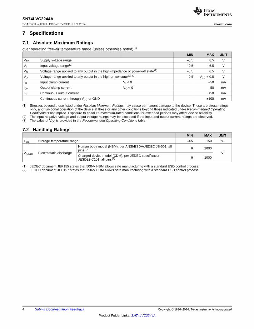
7 Specifications
7.1 Absolute Maximum Ratingsover operating free-air temperature range (unless otherwise noted) (1)
MIN MAX UNITVCC Supply voltage range –0.5 6.5 VVI Input voltage range (2) –0.5 6.5 VVO Voltage range applied to any output in the high-impedance or power-off state (2) –0.5 6.5 VVO Voltage range applied to any output in the high or low state (2) (3) –0.5 VCC + 0.5 VIIK Input clamp current VI < 0 –50 mAIOK Output clamp current VO < 0 –50 mAIO Continuous output current ±50 mA
Continuous current through VCC or GND ±100 mA
(1) Stresses beyond those listed under Absolute Maximum Ratings may cause permanent damage to the device. These are stress ratingsonly, and functional operation of the device at these or any other conditions beyond those indicated under Recommended OperatingConditions is not implied. Exposure to absolute-maximum-rated conditions for extended periods may affect device reliability.
(2) The input negative-voltage and output voltage ratings may be exceeded if the input and output current ratings are observed.(3) The value of VCC is provided in the Recommended Operating Conditions table.
7.2 Handling RatingsMIN MAX UNIT
Tstg Storage temperature range –65 150 °CHuman body model (HBM), per ANSI/ESDA/JEDEC JS-001, all 0 2000pins (1)
V(ESD) Electrostatic discharge VCharged device model (CDM), per JEDEC specification 0 1000JESD22-C101, all pins (2)
(1) JEDEC document JEP155 states that 500-V HBM allows safe manufacturing with a standard ESD control process.(2) JEDEC document JEP157 states that 250-V CDM allows safe manufacturing with a standard ESD control process.
4 Submit Documentation Feedback Copyright © 1996–2014, Texas Instruments Incorporated
Product Folder Links: SN74LVC2244A

SN74LVC2244Awww.ti.com SCAS572L –APRIL 1996–REVISED JULY 2014
7.3 Recommended Operating Conditionsover operating free-air temperature range (unless otherwise noted) (1)
MIN MAX UNITOperating 1.65 3.6
VCC Supply voltage VData retention only 1.5VCC = 1.65 V to 1.95 V 0.65 × VCC
VIH High-level input voltage VCC = 2.3 V to 2.7 V 1.7 VVCC = 2.7 V to 3.6 V 2VCC = 1.65 V to 1.95 V 0.35 × VCC
VIL Low-level input voltage VCC = 2.3 V to 2.7 V 0.7 VVCC = 2.7 V to 3.6 V 0.8
VI Input voltage 0 5.5 VHigh or low state 0 VCCVO Output voltage V3-state 0 5.5VCC = 1.65 V –2VCC = 2.3 V –4
IOH High-level output current mAVCC = 2.7 V –8VCC = 3 V –12VCC = 1.65 V 2VCC = 2.3 V 4
IOL Low-level output current mAVCC = 2.7 V 8VCC = 3 V 12
Δt/Δv Input transition rise or fall rate 10 ns/VTA Operating free-air temperature –40 125 °C
(1) All unused inputs of the device must be held at VCC or GND to ensure proper device operation. Refer to the TI application report,Implications of Slow or Floating CMOS Inputs (SCBA004).
7.4 Thermal InformationSN74LVC2244A
THERMAL METRIC (1) DB DBQ DGV DW NS PW UNIT20 PINS
RθJA Junction-to-ambient thermal resistance 94.5 94.7 114.7 88.3 74.7 102.5RθJC(top) Junction-to-case (top) thermal resistance 56.2 47.9 29.8 51.1 40.5 35.9RθJB Junction-to-board thermal resistance 49.7 45.0 56.2 50.9 42.3 53.5ψJT Junction-to-top characterization parameter 18.1 11.0 0.8 20.0 14.3 2.2 °C/W
Junction-to-board characterizationψJB 49.5 44.6 55.5 50.5 41.9 52.9parameterJunction-to-case (bottom) thermalRθJC(bot) n/a n/a n/a n/a n/a n/aresistance
(1) For more information about traditional and new thermal metrics, see the IC Package Thermal Metrics application report (SPRA953).
Copyright © 1996–2014, Texas Instruments Incorporated Submit Documentation Feedback 5
Product Folder Links: SN74LVC2244A
SN74LVC2244ASCAS572L –APRIL 1996–REVISED JULY 2014 www.ti.com
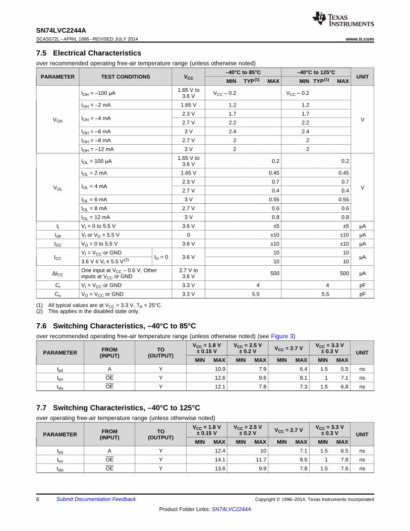
7.5 Electrical Characteristicsover recommended operating free-air temperature range (unless otherwise noted)
–40°C to 85°C –40°C to 125°CPARAMETER TEST CONDITIONS VCC UNIT
MIN TYP (1) MAX MIN TYP (1) MAX1.65 V toIOH = –100 μA VCC – 0.2 VCC – 0.23.6 V
IOH = –2 mA 1.65 V 1.2 1.22.3 V 1.7 1.7
IOH = –4 mAVOH V2.7 V 2.2 2.2IOH = –6 mA 3 V 2.4 2.4IOH = –8 mA 2.7 V 2 2IOH = –12 mA 3 V 2 2
1.65 V toIOL = 100 μA 0.2 0.23.6 VIOL = 2 mA 1.65 V 0.45 0.45
2.3 V 0.7 0.7IOL = 4 mAVOL V2.7 V 0.4 0.4IOL = 6 mA 3 V 0.55 0.55IOL = 8 mA 2.7 V 0.6 0.6IOL = 12 mA 3 V 0.8 0.8
II VI = 0 to 5.5 V 3.6 V ±5 ±5 μAIoff VI or VO = 5.5 V 0 ±10 ±10 μAIOZ VO = 0 to 5.5 V 3.6 V ±10 ±10 μA
VI = VCC or GND 10 10ICC IO = 0 3.6 V μA
3.6 V ≤ VI ≤ 5.5 V (2) 10 10One input at VCC – 0.6 V, Other 2.7 V toΔICC 500 500 μAinputs at VCC or GND 3.6 V
Ci VI = VCC or GND 3.3 V 4 4 pFCo VO = VCC or GND 3.3 V 5.5 5.5 pF
(1) All typical values are at VCC = 3.3 V, TA = 25°C.(2) This applies in the disabled state only.
7.6 Switching Characteristics, –40°C to 85°Cover recommended operating free-air temperature range (unless otherwise noted) (see Figure 3)
VCC = 1.8 V VCC = 2.5 V VCC = 3.3 VVCC = 2.7 VFROM TO ± 0.15 V ± 0.2 V ± 0.3 VPARAMETER UNIT(INPUT) (OUTPUT)MIN MAX MIN MAX MIN MAX MIN MAX
tpd A Y 10.9 7.9 6.4 1.5 5.5 nsten OE Y 12.6 9.6 8.1 1 7.1 nstdis OE Y 12.1 7.8 7.3 1.5 6.8 ns
7.7 Switching Characteristics, –40°C to 125°Cover operating free-air temperature range (unless otherwise noted)
VCC = 1.8 V VCC = 2.5 V VCC = 3.3 VVCC = 2.7 VFROM TO ± 0.15 V ± 0.2 V ± 0.3 VPARAMETER UNIT(INPUT) (OUTPUT)MIN MAX MIN MAX MIN MAX MIN MAX
tpd A Y 12.4 10 7.1 1.5 6.5 nsten OE Y 14.1 11.7 8.5 1 7.8 nstdis OE Y 13.6 9.9 7.8 1.5 7.6 ns
6 Submit Documentation Feedback Copyright © 1996–2014, Texas Instruments Incorporated
Product Folder Links: SN74LVC2244A
Temperature (qC)
TP
D (
ns)
-100 -50 0 50 100 1500
0.5
1
1.5
2
2.5
3
3.5
4
D001
TPD in ns
VCC (V)
TD
P (
ns)
0 0.5 1 1.5 2 2.5 3 3.50
1
2
3
4
5
6
D002
TDP in ns
SN74LVC2244Awww.ti.com SCAS572L –APRIL 1996–REVISED JULY 2014
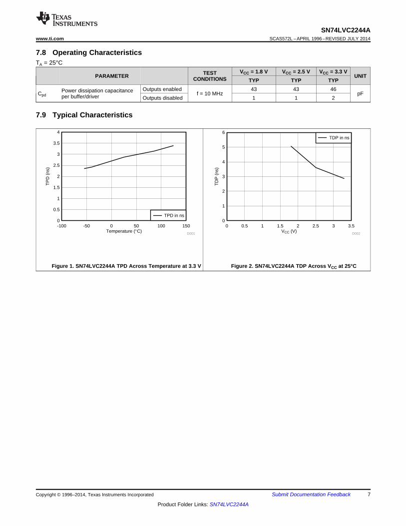
7.8 Operating CharacteristicsTA = 25°C
VCC = 1.8 V VCC = 2.5 V VCC = 3.3 VTESTPARAMETER UNITCONDITIONS TYP TYP TYPOutputs enabled 43 43 46Power dissipation capacitanceCpd f = 10 MHz pFper buffer/driver Outputs disabled 1 1 2
7.9 Typical Characteristics
Figure 1. SN74LVC2244A TPD Across Temperature at 3.3 V Figure 2. SN74LVC2244A TDP Across VCC at 25°C
Copyright © 1996–2014, Texas Instruments Incorporated Submit Documentation Feedback 7
Product Folder Links: SN74LVC2244A
VM
thtsu
From OutputUnder Test
CL(see Note A)
LOAD CIRCUIT
S1VLOAD
Open
GND
RL
RL
Data Input
Timing InputVI
0 V
VI
0 V0 V
tw
Input
VOLTAGE WAVEFORMSSETUP AND HOLD TIMES
VOLTAGE WAVEFORMSPROPAGATION DELAY TIMES
INVERTING AND NONINVERTING OUTPUTS
VOLTAGE WAVEFORMSPULSE DURATION
tPLH
tPHL
tPHL
tPLH
VOH
VOH
VOL
VOL
VI
0 VInput
OutputWaveform 1S1 at VLOAD(see Note B)
OutputWaveform 2
S1 at GND(see Note B)
VOL
VOH
tPZL
tPZH
tPLZ
tPHZ
VLOAD/2
0 V
VOL + V∆
VOH − V∆
≈0 V
VI
VOLTAGE WAVEFORMSENABLE AND DISABLE TIMES
LOW- AND HIGH-LEVEL ENABLING
Output
Output
tPLH/tPHLtPLZ/tPZLtPHZ/tPZH
OpenVLOADGND
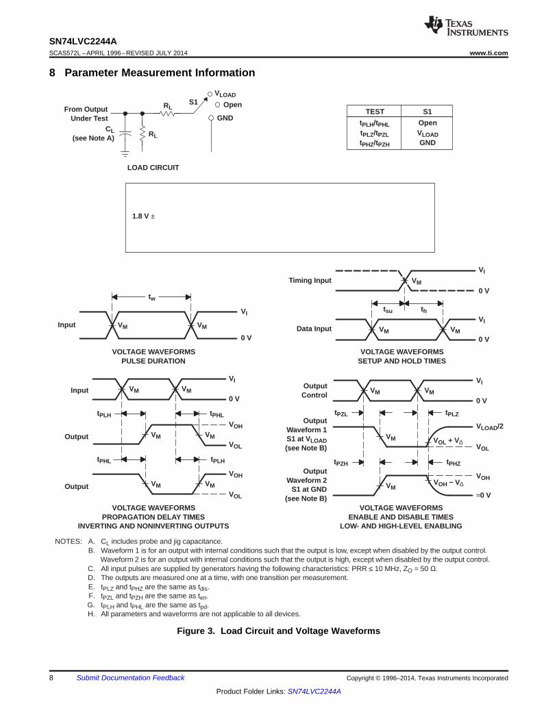
TEST S1
NOTES: A. CL includes probe and jig capacitance.B. Waveform 1 is for an output with internal conditions such that the output is low, except when disabled by the output control.
Waveform 2 is for an output with internal conditions such that the output is high, except when disabled by the output control.C. All input pulses are supplied by generators having the following characteristics: PRR ≤ 10 MHz, ZO = 50 Ω.D. The outputs are measured one at a time, with one transition per measurement.E. tPLZ and tPHZ are the same as tdis.F. tPZL and tPZH are the same as ten.G. tPLH and tPHL are the same as tpd.H. All parameters and waveforms are not applicable to all devices.
OutputControl
VM VM
VM VM
VM VM
VM
VM VM
VM
VM
VM
VI
VM
VM
1.8 V ± 0.15 V2.5 V ± 0.2 V
2.7 V3.3 V ± 0.3 V
1 kΩ500 Ω500 Ω500 Ω
VCC RL
2 × VCC2 × VCC
6 V6 V
VLOAD CL
30 pF30 pF50 pF50 pF
0.15 V0.15 V0.3 V0.3 V
V∆
VCCVCC2.7 V2.7 V
VI
VCC/2VCC/21.5 V1.5 V
VMtr/tf
≤2 ns≤2 ns
≤2.5 ns≤2.5 ns
INPUTS
SN74LVC2244ASCAS572L –APRIL 1996–REVISED JULY 2014 www.ti.com
8 Parameter Measurement Information
Figure 3. Load Circuit and Voltage Waveforms
8 Submit Documentation Feedback Copyright © 1996–2014, Texas Instruments Incorporated
Product Folder Links: SN74LVC2244A

1
2 181Y1
1OE
1A1
4 161Y21A2
6 141Y31A3
8 121Y41A4
19
11 92Y1
2OE
2A1
13 72Y22A2
15 52Y32A3
17 32Y42A4
SN74LVC2244Awww.ti.com SCAS572L –APRIL 1996–REVISED JULY 2014
9 Detailed Description
9.1 OverviewThis octal buffer and line driver is designed for 1.65-V to 3.6-V VCC operation. The SN74LVC2244A device isorganized as two 4-bit line drivers with separate output-enable (OE) inputs. When OE is low, the device passesdata from the A inputs to the Y outputs. When OE is high, the outputs are in the high-impedance state. Theoutputs, which are designed to sink up to 12 mA, include equivalent 26-ohm resistors to reduce overshoot andundershoot.
9.2 Functional Block Diagram
9.3 Feature Description• Wide operating voltage range
– Operates from 1.65 V to 3.6 V• Allows down voltage translation
– Inputs accept voltages to 5.5 V• Ioff Feature
– Allows voltages on the inputs and outputs when VCC is 0 V
9.4 Device Functional Modes
Table 1. Function Table(Each Buffer)
INPUTS OUTPUTYOE A
L H HL L LH X Z
Copyright © 1996–2014, Texas Instruments Incorporated Submit Documentation Feedback 9
Product Folder Links: SN74LVC2244A

µC or
System Logic
OE V
GND
A1
A4
Y1
Y4
Regulated 3.3 V
µC
System Logic
LEDs
CC
SN74LVC2244ASCAS572L –APRIL 1996–REVISED JULY 2014 www.ti.com
10 Application and Implementation
10.1 Application InformationInputs can be driven from either 3.3-V or 5-V devices. This feature allows the use of this device as a translator ina mixed 3.3-V/5-V system environment. This device is fully specified for partial-power-down applications usingIoff. The Ioff circuitry disables the outputs, preventing damaging current backflow through the device when it ispowered down. To ensure the high-impedance state during power up or power down, OE should be tied to VCCthrough a pullup resistor; the minimum value of the resistor is determined by the current-sinking capability of thedriver.
10.2 Typical Application
Figure 4. Typical Application Diagram
10.2.1 Design RequirementsThis device uses CMOS technology and has balanced output drive. Care should be taken to avoid buscontention because it can drive currents that would exceed maximum limits. The high drive will also create fastedges into light loads, so routing and load conditions should be considered to prevent ringing.
10.2.2 Detailed Design Procedure1. Recommended Input Conditions
– Rise time and fall time specs: See (Δt/ΔV) in the Recommended Operating Conditions table.– Specified high and low levels: See (VIH and VIL) in the Recommended Operating Conditions table.– Inputs are overvoltage tolerant allowing them to go as high as 5.5 V at any valid VCC.
2. Recommend Output Conditions– Load currents should not exceed 25 mA per output and 50 mA total for the part.– Outputs should not be pulled above VCC.
10 Submit Documentation Feedback Copyright © 1996–2014, Texas Instruments Incorporated
Product Folder Links: SN74LVC2244A

Vcc
Unused Input
Input
Output
Input
Unused Input Output
Frequency (MHz)
I CC (
mA
)
0 10 20 30 40 50 600
50
100
150
200
250
300
D003
ICC 1.8 VICC 2.5 VICC 3.3 V
SN74LVC2244Awww.ti.com SCAS572L –APRIL 1996–REVISED JULY 2014
Typical Application (continued)10.2.3 Application Curves
Figure 5. ICC vs Frequency
11 Power Supply RecommendationsThe power supply can be any voltage between the MIN and MAX supply voltage rating located in theRecommended Operating Conditions table.
Each VCC pin should have a good bypass capacitor to prevent power disturbance. For devices with a singlesupply, 0.1 μf is recommended; if there are multiple VCC pins, then 0.01 μf or 0.022 μf is recommended for eachpower pin. It is acceptable to parallel multiple bypass caps to reject different frequencies of noise. A 0.1 μf and a1 μf are commonly used in parallel. The bypass capacitor should be installed as close to the power pin aspossible for best results.
12 Layout
12.1 Layout GuidelinesWhen using multiple-bit logic devices, inputs should never float.
In many cases, functions or parts of functions of digital logic devices are unused, for example, when only twoinputs of a triple-input AND gate are used or only 3 of the 4 buffer gates are used. Such input pins should not beleft unconnected because the undefined voltages at the outside connections result in undefined operationalstates. Figure 6 specifies the rules that must be observed under all circumstances. All unused inputs of digitallogic devices must be connected to a high or low bias to prevent them from floating. The logic level that shouldbe applied to any particular unused input depends on the function of the device. Generally they will be tied toGND or VCC, whichever makes more sense or is more convenient. It is generally acceptable to float outputs,unless the part is a transceiver. If the transceiver has an output enable pin, it will disable the output section of thepart when asserted. This will not disable the input section of the IOs, so they cannot float when disabled.
12.2 Layout Example
Figure 6. Layout Diagram
Copyright © 1996–2014, Texas Instruments Incorporated Submit Documentation Feedback 11
Product Folder Links: SN74LVC2244A

SN74LVC2244ASCAS572L –APRIL 1996–REVISED JULY 2014 www.ti.com
13 Device and Documentation Support
13.1 TrademarksAll trademarks are the property of their respective owners.
13.2 Electrostatic Discharge CautionThese devices have limited built-in ESD protection. The leads should be shorted together or the device placed in conductive foamduring storage or handling to prevent electrostatic damage to the MOS gates.
13.3 GlossarySLYZ022 — TI Glossary.
This glossary lists and explains terms, acronyms, and definitions.
14 Mechanical, Packaging, and Orderable InformationThe following pages include mechanical, packaging, and orderable information. This information is the mostcurrent data available for the designated devices. This data is subject to change without notice and revision ofthis document. For browser-based versions of this data sheet, refer to the left-hand navigation.
12 Submit Documentation Feedback Copyright © 1996–2014, Texas Instruments Incorporated
Product Folder Links: SN74LVC2244A

PACKAGE OPTION ADDENDUM
www.ti.com 17-Mar-2017
Addendum-Page 1
PACKAGING INFORMATION
Orderable Device Status(1)
Package Type PackageDrawing
Pins PackageQty
Eco Plan(2)
Lead/Ball Finish(6)
MSL Peak Temp(3)
Op Temp (°C) Device Marking(4/5)
Samples
SN74LVC2244ADBQR ACTIVE SSOP DBQ 20 2500 Green (RoHS& no Sb/Br)
CU NIPDAU Level-2-260C-1 YEAR -40 to 85 LVC2244A
SN74LVC2244ADBQRE4 ACTIVE SSOP DBQ 20 2500 Green (RoHS& no Sb/Br)
CU NIPDAU Level-2-260C-1 YEAR -40 to 85 LVC2244A
SN74LVC2244ADBR ACTIVE SSOP DB 20 2000 Green (RoHS& no Sb/Br)
CU NIPDAU Level-1-260C-UNLIM -40 to 85 LE244A
SN74LVC2244ADBRG4 ACTIVE SSOP DB 20 2000 Green (RoHS& no Sb/Br)
CU NIPDAU Level-1-260C-UNLIM -40 to 85 LE244A
SN74LVC2244ADGVR ACTIVE TVSOP DGV 20 2000 Green (RoHS& no Sb/Br)
CU NIPDAU Level-1-260C-UNLIM -40 to 85 LE244A
SN74LVC2244ADGVRE4 ACTIVE TVSOP DGV 20 2000 Green (RoHS& no Sb/Br)
CU NIPDAU Level-1-260C-UNLIM -40 to 85 LE244A
SN74LVC2244ADW ACTIVE SOIC DW 20 25 Green (RoHS& no Sb/Br)
CU NIPDAU Level-1-260C-UNLIM -40 to 85 LVC2244A
SN74LVC2244ADWR ACTIVE SOIC DW 20 2000 Green (RoHS& no Sb/Br)
CU NIPDAU Level-1-260C-UNLIM -40 to 85 LVC2244A
SN74LVC2244ADWRE4 ACTIVE SOIC DW 20 2000 Green (RoHS& no Sb/Br)
CU NIPDAU Level-1-260C-UNLIM -40 to 85 LVC2244A
SN74LVC2244ADWRG4 ACTIVE SOIC DW 20 2000 Green (RoHS& no Sb/Br)
CU NIPDAU Level-1-260C-UNLIM -40 to 85 LVC2244A
SN74LVC2244ANSR ACTIVE SO NS 20 2000 Green (RoHS& no Sb/Br)
CU NIPDAU Level-1-260C-UNLIM -40 to 85 LVC2244A
SN74LVC2244ANSRG4 ACTIVE SO NS 20 2000 Green (RoHS& no Sb/Br)
CU NIPDAU Level-1-260C-UNLIM -40 to 85 LVC2244A
SN74LVC2244APW ACTIVE TSSOP PW 20 70 Green (RoHS& no Sb/Br)
CU NIPDAU Level-1-260C-UNLIM -40 to 85 LE244A
SN74LVC2244APWG4 ACTIVE TSSOP PW 20 70 Green (RoHS& no Sb/Br)
CU NIPDAU Level-1-260C-UNLIM -40 to 85 LE244A
SN74LVC2244APWR ACTIVE TSSOP PW 20 2000 Green (RoHS& no Sb/Br)
CU NIPDAU Level-1-260C-UNLIM -40 to 85 LE244A
SN74LVC2244APWRE4 ACTIVE TSSOP PW 20 2000 Green (RoHS& no Sb/Br)
CU NIPDAU Level-1-260C-UNLIM -40 to 85 LE244A
SN74LVC2244APWRG4 ACTIVE TSSOP PW 20 2000 Green (RoHS& no Sb/Br)
CU NIPDAU Level-1-260C-UNLIM -40 to 85 LE244A

PACKAGE OPTION ADDENDUM
www.ti.com 17-Mar-2017
Addendum-Page 2
Orderable Device Status(1)
Package Type PackageDrawing
Pins PackageQty
Eco Plan(2)
Lead/Ball Finish(6)
MSL Peak Temp(3)
Op Temp (°C) Device Marking(4/5)
Samples
SN74LVC2244APWT ACTIVE TSSOP PW 20 250 Green (RoHS& no Sb/Br)
CU NIPDAU Level-1-260C-UNLIM -40 to 85 LE244A
(1) The marketing status values are defined as follows:ACTIVE: Product device recommended for new designs.LIFEBUY: TI has announced that the device will be discontinued, and a lifetime-buy period is in effect.NRND: Not recommended for new designs. Device is in production to support existing customers, but TI does not recommend using this part in a new design.PREVIEW: Device has been announced but is not in production. Samples may or may not be available.OBSOLETE: TI has discontinued the production of the device.
(2) Eco Plan - The planned eco-friendly classification: Pb-Free (RoHS), Pb-Free (RoHS Exempt), or Green (RoHS & no Sb/Br) - please check http://www.ti.com/productcontent for the latest availabilityinformation and additional product content details.TBD: The Pb-Free/Green conversion plan has not been defined.Pb-Free (RoHS): TI's terms "Lead-Free" or "Pb-Free" mean semiconductor products that are compatible with the current RoHS requirements for all 6 substances, including the requirement thatlead not exceed 0.1% by weight in homogeneous materials. Where designed to be soldered at high temperatures, TI Pb-Free products are suitable for use in specified lead-free processes.Pb-Free (RoHS Exempt): This component has a RoHS exemption for either 1) lead-based flip-chip solder bumps used between the die and package, or 2) lead-based die adhesive used betweenthe die and leadframe. The component is otherwise considered Pb-Free (RoHS compatible) as defined above.Green (RoHS & no Sb/Br): TI defines "Green" to mean Pb-Free (RoHS compatible), and free of Bromine (Br) and Antimony (Sb) based flame retardants (Br or Sb do not exceed 0.1% by weightin homogeneous material)
(3) MSL, Peak Temp. - The Moisture Sensitivity Level rating according to the JEDEC industry standard classifications, and peak solder temperature.
(4) There may be additional marking, which relates to the logo, the lot trace code information, or the environmental category on the device.
(5) Multiple Device Markings will be inside parentheses. Only one Device Marking contained in parentheses and separated by a "~" will appear on a device. If a line is indented then it is a continuationof the previous line and the two combined represent the entire Device Marking for that device.
(6) Lead/Ball Finish - Orderable Devices may have multiple material finish options. Finish options are separated by a vertical ruled line. Lead/Ball Finish values may wrap to two lines if the finishvalue exceeds the maximum column width.
Important Information and Disclaimer:The information provided on this page represents TI's knowledge and belief as of the date that it is provided. TI bases its knowledge and belief on informationprovided by third parties, and makes no representation or warranty as to the accuracy of such information. Efforts are underway to better integrate information from third parties. TI has taken andcontinues to take reasonable steps to provide representative and accurate information but may not have conducted destructive testing or chemical analysis on incoming materials and chemicals.TI and TI suppliers consider certain information to be proprietary, and thus CAS numbers and other limited information may not be available for release.
In no event shall TI's liability arising out of such information exceed the total purchase price of the TI part(s) at issue in this document sold by TI to Customer on an annual basis.

TAPE AND REEL INFORMATION
*All dimensions are nominal
Device PackageType
PackageDrawing
Pins SPQ ReelDiameter
(mm)
ReelWidth
W1 (mm)
A0(mm)
B0(mm)
K0(mm)
P1(mm)
W(mm)
Pin1Quadrant
SN74LVC2244ADBQR SSOP DBQ 20 2500 330.0 16.4 6.5 9.0 2.1 8.0 16.0 Q1
SN74LVC2244ADBR SSOP DB 20 2000 330.0 16.4 8.2 7.5 2.5 12.0 16.0 Q1
SN74LVC2244ADGVR TVSOP DGV 20 2000 330.0 12.4 6.9 5.6 1.6 8.0 12.0 Q1
SN74LVC2244ADWR SOIC DW 20 2000 330.0 24.4 10.8 13.3 2.7 12.0 24.0 Q1
SN74LVC2244ANSR SO NS 20 2000 330.0 24.4 8.4 13.0 2.5 12.0 24.0 Q1
SN74LVC2244APWR TSSOP PW 20 2000 330.0 16.4 6.95 7.1 1.6 8.0 16.0 Q1
SN74LVC2244APWT TSSOP PW 20 250 330.0 16.4 6.95 7.1 1.6 8.0 16.0 Q1
PACKAGE MATERIALS INFORMATION
www.ti.com 6-May-2017
Pack Materials-Page 1
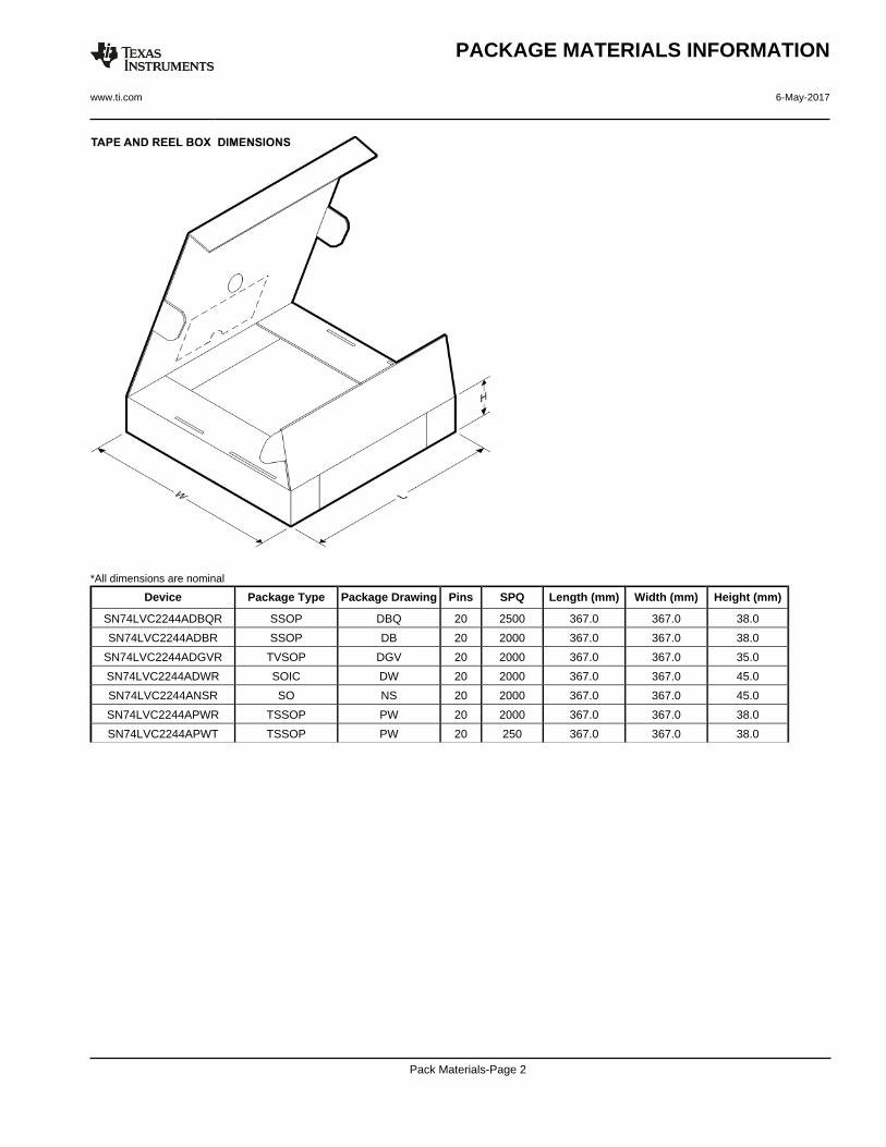
*All dimensions are nominal
Device Package Type Package Drawing Pins SPQ Length (mm) Width (mm) Height (mm)
SN74LVC2244ADBQR SSOP DBQ 20 2500 367.0 367.0 38.0
SN74LVC2244ADBR SSOP DB 20 2000 367.0 367.0 38.0
SN74LVC2244ADGVR TVSOP DGV 20 2000 367.0 367.0 35.0
SN74LVC2244ADWR SOIC DW 20 2000 367.0 367.0 45.0
SN74LVC2244ANSR SO NS 20 2000 367.0 367.0 45.0
SN74LVC2244APWR TSSOP PW 20 2000 367.0 367.0 38.0
SN74LVC2244APWT TSSOP PW 20 250 367.0 367.0 38.0
PACKAGE MATERIALS INFORMATION
www.ti.com 6-May-2017
Pack Materials-Page 2
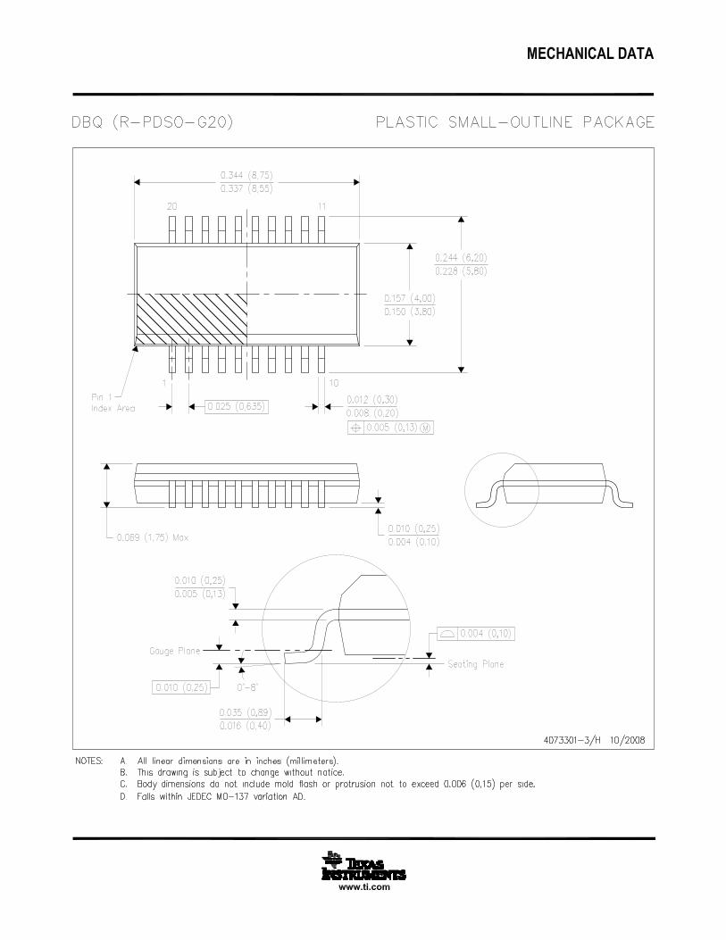

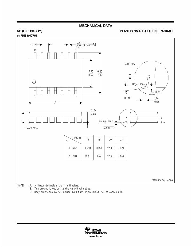
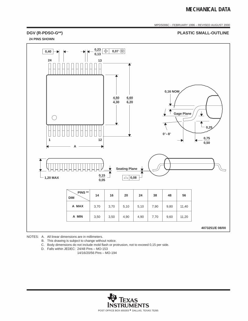
MECHANICAL DATA
MPDS006C – FEBRUARY 1996 – REVISED AUGUST 2000
POST OFFICE BOX 655303 • DALLAS, TEXAS 75265
DGV (R-PDSO-G**) PLASTIC SMALL-OUTLINE 24 PINS SHOWN
14
3,70
3,50 4,90
5,10
20DIM
PINS **
4073251/E 08/00
1,20 MAX
Seating Plane
0,050,15
0,25
0,500,75
0,230,13
1 12
24 13
4,304,50
0,16 NOM
Gage Plane
A
7,90
7,70
382416
4,90
5,103,70
3,50
A MAX
A MIN
6,606,20
11,20
11,40
56
9,60
9,80
48
0,08
M0,070,40
0°–8°
NOTES: A. All linear dimensions are in millimeters.B. This drawing is subject to change without notice.C. Body dimensions do not include mold flash or protrusion, not to exceed 0,15 per side.D. Falls within JEDEC: 24/48 Pins – MO-153
14/16/20/56 Pins – MO-194

MECHANICAL DATA
MSSO002E – JANUARY 1995 – REVISED DECEMBER 2001
POST OFFICE BOX 655303 • DALLAS, TEXAS 75265
DB (R-PDSO-G**) PLASTIC SMALL-OUTLINE
4040065 /E 12/01
28 PINS SHOWN
Gage Plane
8,207,40
0,550,95
0,25
38
12,90
12,30
28
10,50
24
8,50
Seating Plane
9,907,90
30
10,50
9,90
0,38
5,605,00
15
0,22
14
A
28
1
2016
6,506,50
14
0,05 MIN
5,905,90
DIM
A MAX
A MIN
PINS **
2,00 MAX
6,90
7,50
0,65 M0,15
0°–8°
0,10
0,090,25
NOTES: A. All linear dimensions are in millimeters.B. This drawing is subject to change without notice.C. Body dimensions do not include mold flash or protrusion not to exceed 0,15.D. Falls within JEDEC MO-150
www.ti.com
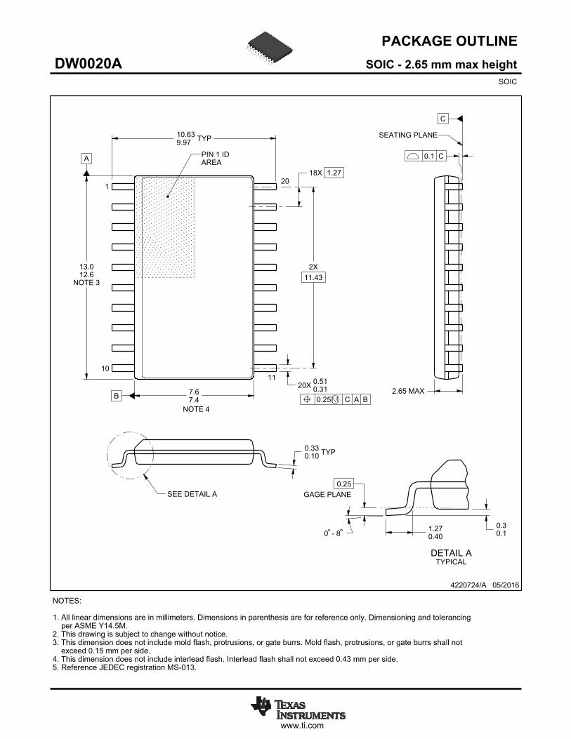
PACKAGE OUTLINE
C
TYP10.639.97
2.65 MAX
18X 1.27
20X 0.510.31
2X11.43
TYP0.330.10
0 - 80.30.1
0.25GAGE PLANE
1.270.40
A
NOTE 3
13.012.6
B 7.67.4
4220724/A 05/2016
SOIC - 2.65 mm max heightDW0020ASOIC
NOTES: 1. All linear dimensions are in millimeters. Dimensions in parenthesis are for reference only. Dimensioning and tolerancing per ASME Y14.5M. 2. This drawing is subject to change without notice. 3. This dimension does not include mold flash, protrusions, or gate burrs. Mold flash, protrusions, or gate burrs shall not exceed 0.15 mm per side. 4. This dimension does not include interlead flash. Interlead flash shall not exceed 0.43 mm per side.5. Reference JEDEC registration MS-013.
120
0.25 C A B
1110
PIN 1 IDAREA
NOTE 4
SEATING PLANE
0.1 C
SEE DETAIL A
DETAIL ATYPICAL
SCALE 1.200

www.ti.com
EXAMPLE BOARD LAYOUT
(9.3)
0.07 MAXALL AROUND
0.07 MINALL AROUND
20X (2)
20X (0.6)
18X (1.27)
(R )TYP
0.05
4220724/A 05/2016
SOIC - 2.65 mm max heightDW0020ASOIC
SYMM
SYMM
LAND PATTERN EXAMPLESCALE:6X
1
10 11
20
NOTES: (continued) 6. Publication IPC-7351 may have alternate designs. 7. Solder mask tolerances between and around signal pads can vary based on board fabrication site.
METALSOLDER MASKOPENING
NON SOLDER MASKDEFINED
SOLDER MASK DETAILS
SOLDER MASKOPENING
METAL UNDERSOLDER MASK
SOLDER MASKDEFINED
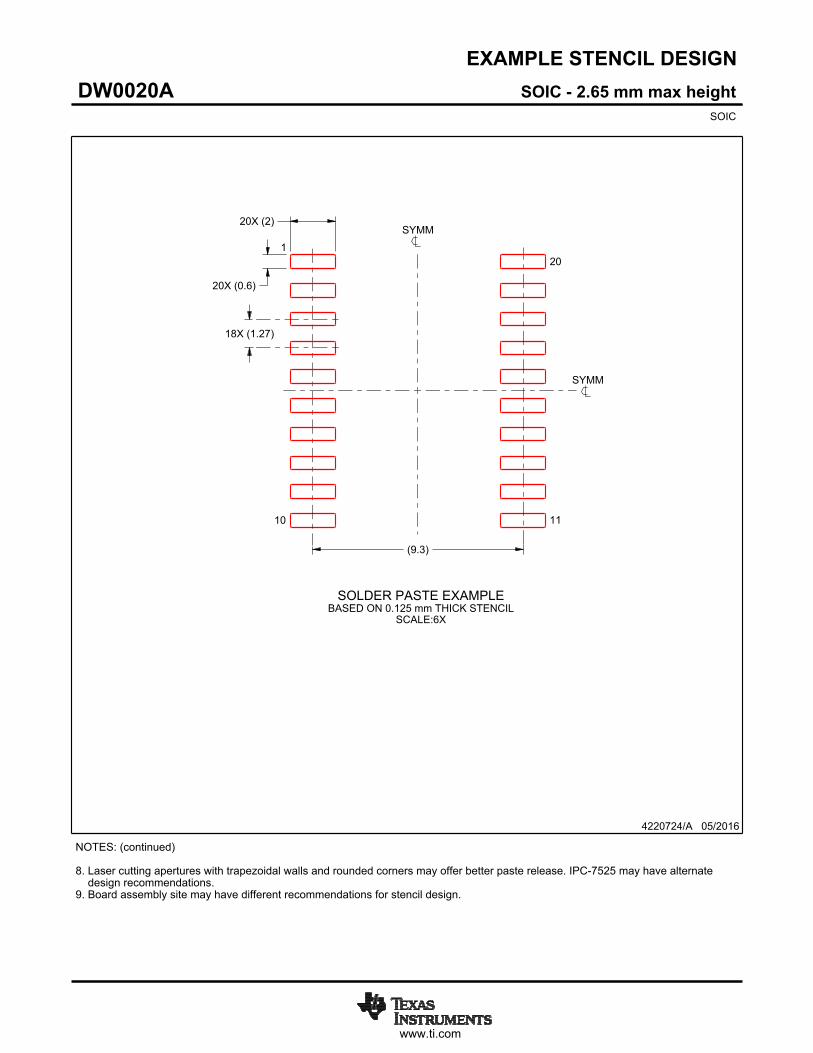
www.ti.com
EXAMPLE STENCIL DESIGN
(9.3)
18X (1.27)
20X (0.6)
20X (2)
4220724/A 05/2016
SOIC - 2.65 mm max heightDW0020ASOIC
NOTES: (continued) 8. Laser cutting apertures with trapezoidal walls and rounded corners may offer better paste release. IPC-7525 may have alternate design recommendations. 9. Board assembly site may have different recommendations for stencil design.
SYMM
SYMM
1
10 11
20
SOLDER PASTE EXAMPLEBASED ON 0.125 mm THICK STENCIL
SCALE:6X

IMPORTANT NOTICE
Texas Instruments Incorporated (TI) reserves the right to make corrections, enhancements, improvements and other changes to itssemiconductor products and services per JESD46, latest issue, and to discontinue any product or service per JESD48, latest issue. Buyersshould obtain the latest relevant information before placing orders and should verify that such information is current and complete.TI’s published terms of sale for semiconductor products (http://www.ti.com/sc/docs/stdterms.htm) apply to the sale of packaged integratedcircuit products that TI has qualified and released to market. Additional terms may apply to the use or sale of other types of TI products andservices.Reproduction of significant portions of TI information in TI data sheets is permissible only if reproduction is without alteration and isaccompanied by all associated warranties, conditions, limitations, and notices. TI is not responsible or liable for such reproduceddocumentation. Information of third parties may be subject to additional restrictions. Resale of TI products or services with statementsdifferent from or beyond the parameters stated by TI for that product or service voids all express and any implied warranties for theassociated TI product or service and is an unfair and deceptive business practice. TI is not responsible or liable for any such statements.Buyers and others who are developing systems that incorporate TI products (collectively, “Designers”) understand and agree that Designersremain responsible for using their independent analysis, evaluation and judgment in designing their applications and that Designers havefull and exclusive responsibility to assure the safety of Designers' applications and compliance of their applications (and of all TI productsused in or for Designers’ applications) with all applicable regulations, laws and other applicable requirements. Designer represents that, withrespect to their applications, Designer has all the necessary expertise to create and implement safeguards that (1) anticipate dangerousconsequences of failures, (2) monitor failures and their consequences, and (3) lessen the likelihood of failures that might cause harm andtake appropriate actions. Designer agrees that prior to using or distributing any applications that include TI products, Designer willthoroughly test such applications and the functionality of such TI products as used in such applications.TI’s provision of technical, application or other design advice, quality characterization, reliability data or other services or information,including, but not limited to, reference designs and materials relating to evaluation modules, (collectively, “TI Resources”) are intended toassist designers who are developing applications that incorporate TI products; by downloading, accessing or using TI Resources in anyway, Designer (individually or, if Designer is acting on behalf of a company, Designer’s company) agrees to use any particular TI Resourcesolely for this purpose and subject to the terms of this Notice.TI’s provision of TI Resources does not expand or otherwise alter TI’s applicable published warranties or warranty disclaimers for TIproducts, and no additional obligations or liabilities arise from TI providing such TI Resources. TI reserves the right to make corrections,enhancements, improvements and other changes to its TI Resources. TI has not conducted any testing other than that specificallydescribed in the published documentation for a particular TI Resource.Designer is authorized to use, copy and modify any individual TI Resource only in connection with the development of applications thatinclude the TI product(s) identified in such TI Resource. NO OTHER LICENSE, EXPRESS OR IMPLIED, BY ESTOPPEL OR OTHERWISETO ANY OTHER TI INTELLECTUAL PROPERTY RIGHT, AND NO LICENSE TO ANY TECHNOLOGY OR INTELLECTUAL PROPERTYRIGHT OF TI OR ANY THIRD PARTY IS GRANTED HEREIN, including but not limited to any patent right, copyright, mask work right, orother intellectual property right relating to any combination, machine, or process in which TI products or services are used. Informationregarding or referencing third-party products or services does not constitute a license to use such products or services, or a warranty orendorsement thereof. Use of TI Resources may require a license from a third party under the patents or other intellectual property of thethird party, or a license from TI under the patents or other intellectual property of TI.TI RESOURCES ARE PROVIDED “AS IS” AND WITH ALL FAULTS. TI DISCLAIMS ALL OTHER WARRANTIES ORREPRESENTATIONS, EXPRESS OR IMPLIED, REGARDING RESOURCES OR USE THEREOF, INCLUDING BUT NOT LIMITED TOACCURACY OR COMPLETENESS, TITLE, ANY EPIDEMIC FAILURE WARRANTY AND ANY IMPLIED WARRANTIES OFMERCHANTABILITY, FITNESS FOR A PARTICULAR PURPOSE, AND NON-INFRINGEMENT OF ANY THIRD PARTY INTELLECTUALPROPERTY RIGHTS. TI SHALL NOT BE LIABLE FOR AND SHALL NOT DEFEND OR INDEMNIFY DESIGNER AGAINST ANY CLAIM,INCLUDING BUT NOT LIMITED TO ANY INFRINGEMENT CLAIM THAT RELATES TO OR IS BASED ON ANY COMBINATION OFPRODUCTS EVEN IF DESCRIBED IN TI RESOURCES OR OTHERWISE. IN NO EVENT SHALL TI BE LIABLE FOR ANY ACTUAL,DIRECT, SPECIAL, COLLATERAL, INDIRECT, PUNITIVE, INCIDENTAL, CONSEQUENTIAL OR EXEMPLARY DAMAGES INCONNECTION WITH OR ARISING OUT OF TI RESOURCES OR USE THEREOF, AND REGARDLESS OF WHETHER TI HAS BEENADVISED OF THE POSSIBILITY OF SUCH DAMAGES.Unless TI has explicitly designated an individual product as meeting the requirements of a particular industry standard (e.g., ISO/TS 16949and ISO 26262), TI is not responsible for any failure to meet such industry standard requirements.Where TI specifically promotes products as facilitating functional safety or as compliant with industry functional safety standards, suchproducts are intended to help enable customers to design and create their own applications that meet applicable functional safety standardsand requirements. Using products in an application does not by itself establish any safety features in the application. Designers mustensure compliance with safety-related requirements and standards applicable to their applications. Designer may not use any TI products inlife-critical medical equipment unless authorized officers of the parties have executed a special contract specifically governing such use.Life-critical medical equipment is medical equipment where failure of such equipment would cause serious bodily injury or death (e.g., lifesupport, pacemakers, defibrillators, heart pumps, neurostimulators, and implantables). Such equipment includes, without limitation, allmedical devices identified by the U.S. Food and Drug Administration as Class III devices and equivalent classifications outside the U.S.TI may expressly designate certain products as completing a particular qualification (e.g., Q100, Military Grade, or Enhanced Product).Designers agree that it has the necessary expertise to select the product with the appropriate qualification designation for their applicationsand that proper product selection is at Designers’ own risk. Designers are solely responsible for compliance with all legal and regulatoryrequirements in connection with such selection.Designer will fully indemnify TI and its representatives against any damages, costs, losses, and/or liabilities arising out of Designer’s non-compliance with the terms and provisions of this Notice.
Mailing Address: Texas Instruments, Post Office Box 655303, Dallas, Texas 75265Copyright © 2017, Texas Instruments Incorporated


![[Hanyu] Elementary Chinese Readers 3 (Revised Edition) Sinolingua 1996](https://img.pdfslide.us/doc/110x75/55cf9cca550346d033ab0d47/hanyu-elementary-chinese-readers-3-revised-edition-sinolingua-1996.jpg)