Embed Size (px)
Citation preview
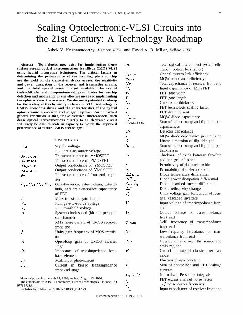
IEEE JOURNAL OF SELECTED TOPICS IN QUANTUM ELECTRONICS, VOL. 2, NO. 1, APRIL 1996 55
Scaling Optoelectronic-VLSI Circuits intothe 21st Century: A Technology Roadmap
Ashok V. Krishnamoorthy,Member, IEEE,and David A. B. Miller, Fellow, IEEE
Abstract— Technologies now exist for implementing densesurface-normal optical interconnections for silicon CMOS VLSIusing hybrid integration techniques. The critical factors indetermining the performance of the resulting photonic chipare the yield on the transceiver device arrays, the sensitivityand power dissipation of the receiver and transmitter circuits,and the total optical power budget available. The use ofGaAs–AlGaAs multiple-quantum-well p-i-n diodes for on-chipdetection and modulation is one effective means of implementingthe optoelectronic transceivers. We discuss a potential roadmapfor the scaling of this hybrid optoelectronic VLSI technology asCMOS linewidths shrink and the characteristics of the hybridoptoelectronic tranceiver technology improve. An importantgeneral conclusion is that, unlike electrical interconnects, suchdense optical interconnections directly to an electronic circuitwill likely be able to scale in capacity to match the improvedperformance of future CMOS technology.
NOMENCLATURE
Supply voltageFET drain-to-source voltageTransconductance of MOSFETTransconductance of MOSFETOutput conductance of MOSFETOutput conductance of MOSFETTransconductance of front-end ampli-fierGate-to-source, gate-to-drain, gate-to-bulk, and drain-to-source capacitanceof FETMOS transistor gain factorFET gate-to-source voltageFET threshold voltageSystem clock-speed (bit rate per opti-cal channel)RMS noise current of CMOS receiverfront endUnity-gain frequency of MOS transis-torOpen-loop gain of CMOS inverterstageImpedance of transimpedance feed-back elementPeak input photocurrentCurrent in biased transimpedancefront-end stage
Manuscript received March 15, 1996; revised August 13, 1996.The authors are with Bell Laboratories, Lucent Technologies, Holmdel, NJ
07733 USA.Publisher Item Identifier S 1077-260X(96)08126-9.
Total optical interconnect system effi-ciency (optical loss factor)Optical system link efficiencyMQW modulator efficiencyTotal capacitance of receiver front endInput capacitance of MOSFETFET gate widthFET gate lengthGate oxide thicknessFET technology scaling factorFET drain currentMQW diode capacitanceSum of solder-bump and flip-chip padcapacitancesDetector capacitanceMQW diode capacitance per unit areaLinear dimension of flip-chip padSum of solder-bump and flip-chip padthicknessesThickness of oxide between flip-chippad and ground planePermittivity of dielectric oxidePermiability of dielectric oxideDiode temperature differentialDiode power dissipation differentialDiode absorbed current differentialDiode reflectivity changeUnity voltage gain bandwidth of iden-tical cascaded invertersInput voltage of transimpedance frontendOutput voltage of transimpedancefront end3-dB frequency of transimpedancefront endLow-frequency impedance of tran-simpedance front endOverlap of gate over the source anddrain regionsCut-off bit rate of classical receivermodelElectron charge constantSum of photodiode and FET leakagecurrentsNormalized Personick integralsFET excess channel noise factor
noise corner frequencyInput capacitance of receiver front end
1077–260X/96$05.00 1996 IEEE
56 IEEE JOURNAL OF SELECTED TOPICS IN QUANTUM ELECTRONICS, VOL. 2, NO. 1, APRIL 1996
FET channel length modulation pa-rameterDetector responsivityOutput capacitance of transimpedancefront endFeedback capacitance of tran-simpedance front endTotal transmitter capacitance includingdiodes and driverOutput resistance of transimpedancefront endLoad capacitance of amplifier stagefollowing front endFET subthreshold leakage currentFET drain-current at onset of satura-tionSubthreshold conduction slopeDuration of bitInput voltage swing at receiver frontendAverage optical power in received in-putNumber of transmitted bitsNumber of light pulsesMQW bias voltageNormalized modulator power effi-ciency of high-reflectivity stateNormalized modulator power effi-ciency of low-reflectivity statePower dissipation of receiver circuitPower dissipation of transmitter circuitThermal resistance of NQW diodeOptical energy-per-bit at receiverOperating temperature
I. INTRODUCTION
T HE tremendous progress in high-performance very-large-scale integrated circuit (VLSI) technology has made
possible the incorporation of several million transistors ontoa single silicon chip with on-chip clock rates of over 400MHz. By 2001, the integration density for silicon complemen-tary metal oxide semiconductor (CMOS) field-effect transistor(FET) logic is expected to be up to 13 million transistors andthe projected on-chip clock rate to be 600 MHz [1]. Recentestimates made by the Semiconductor Industry Associationindicate that the number of transistors available for logic chipsand memory chips will respectively double and quadrupleevery three years. Two factors drive this trend: the shrinkingfeature size of silicon VLSI, resulting in a higher density ofgates per unit area, and the improving yield of integratedcircuits, resulting in more silicon real estate per chip. Theenormous bandwidth that will be available for computationand switching on a silicon integrated circuit will create anincreasing demand for high-bandwidth input and output (I/O)to a VLSI circuit. Novel interconnect technologies will beneeded to meet this challenge.
One possible solution is the use of three-dimensional (3-D)optical interconnect technologies via surface-normal optical
transmitters and receivers. Hybrid integration of several light-transmitter technologies has been investigated for paralleloptical interconnections to silicon. These include electroopticpolarization modulators such as ferro-electric liquid crystal(FLC) and lead-lanthanum-zirconium-titanate (PLZT) mod-ulators [2]–[5], indium-phosphide light emitting diodes [6],surface-emitting lasers [7]–[10], and gallium-arsenide (GaAs)multiple-quantum-well (MQW) electroabsorption modulators[11]–[16].
The integration of GaAs–AlGaAs p-i(MQW)-n diodes toCMOS circuits provides the ability to both transmit and receivedata optically. This can be accomplished by flip-chip bond-ing photodetectors and light-modulators onto a prefabricatedsilicon integrated circuit containing receiver and transmitter(modulator) driver circuits. The attachment operation is fol-lowed by substrate removal of the GaAs chip, which allowsthe modulators to operate at a wavelength of approximately850 nm [17]. The intimate connection between these optoelec-tronic MQW diodes and commodity CMOS devices representsan important step in the evolution of self-electrooptic-effectdevice (SEED) technology [18]. This method has been usedto fabricate high-density optically interconnected submicronCMOS integrated circuits by bonding directly above activesilicon gates [19], [20]. This technique effectively decouplesthe design of the silicon from the placement and bonding of thesurface-normal optical I/O, making the technology more ac-cessible to a system architect, and allowing high-performancesilicon design tools to be used for rapid prototyping ofoptoelectronic circuits.
Arrays of four thousand operational optical devices cannow be bonded to a single CMOS chip [21]. Individualtransimpedance receiver/transmitter circuits, based on two-beam differential data encoding, have been built in 0.8-mCMOS and are capable of 1 Gb/s transmission of digitaldata at a bit-error rate below [22]. These results suggestthat free-space optical interconnect technologies could soonprovide over a terabit-per-second of optical input/output toa conventional silicon VLSI integrated circuit. Although caremust be taken in comparing a research-level optical technologyagainst a commodity electrical one, it is by no means clear thatthe electrical interconnect technology is practical for Tb/s orhigher capacities, especially on and off a single chip.
The emergence of this integration technology and allied fiberand free-space optical technologies for steering and focusinglight beams presents new opportunities and challenges to thesystem designer. One particular opportunity is that opticalinterconnections do not have the problem that their bit-ratecapacity falls off rapidly with distance; electrical intercon-nections quite generally have a bit-rate capacity that fallsas the square of the length for a given cross-sectional area[23],1 making long, thin, high-speed electrical interconnectsimpractical. Optical interconnections will allow densities ofinformation flow much larger than the few Gb/s/cmtypicalof connectorized coaxial cable a few meters in length. In fact,the use of optics with the hybrid CMOS-MQW modulator
1This scaling limit arises both in high-speed (e.g., coaxial) cables andstriplines limited by skin-effect losses and also in the resistive/capacitive linesfound on chips.
KRISHNAMOORTHY AND MILLER: SCALING OPTOELECTRONIC-VLSI CIRCUITS INTO THE 21ST CENTURY 57
technology described here allows large numbers of high-speedconnection directly to and from a single chip to cabinets thatare meters away, a concept that is not feasible electrically athigh bit rates.
In this paper, we present a roadmap that will detail a possibleevolution of this optoelectronic-VLSI (OE-VLSI) technologyas silicon feature sizes shrink, and the dimensions of theGaAs–AlGaAs MQW diodes are reduced. The main objectivesare: 1) to delineate an anticipateddesign-spacefor smart-pixel systems that are based on OE-VLSI circuits used inconjunction with free-space optical interconnects; and 2) toexpose potential technology and circuit design challenges thatwill allow the boundaries of this design space to be met or evenexceeded. The progress of silicon CMOS technology is ex-pected to follow the projections of the Semiconductor IndustryAssociation (SIA) roadmap [1]. Assumptions are made for theexpected evolution of the accompanying optoelectronic MQWdevices. Based on these data, and certain assumptions on theavailability of sufficient laser power to drive the optoelectronicdevices, the system loss budget, and ability to dissipate thepower consumed on-chip, we project limits on the maximumnumber of optical I/O and the electrical circuit complexityper optical I/O for current and future generations of OE-VLSIchips. For projections of optical and optoelectronic device per-formance and yield, where there is no roadmap comparable tothe SIA electronic roadmap, we have been very conservative inanticipating the capability of future optical and optoelectronictechnologies. In many cases, the “predictions” of some futureperformance fall substantially below current research results;this is deliberate because we are interested in credible pro-jections of performance for systems that could realistically bemanufactured at reasonable cost. Section II reviews the deviceassumptions. Section III summarizes methodology used in thispaper. Section IV discusses the receiver model assumed forthis study and presents the derivation for the maximum numberof optical receivers. Results of the study are presented inSection V. A summary and conclusions constitutes Section VI.
II. TECHNOLOGY ASSUMPTIONS
The performance limits of the optoelectronic VLSI technol-ogy can be expressed in terms of: 1) the maximum number ofoptical I/O; 2) the bandwidth per I/O; and 3) the complexity (interms of the number of transistors or gates) per optical I/O. Wewill attempt to quantify these expressions and expose tradeoffsthat may occur between these quantities. In general, theperformance-limiting factors typically include: 1) the availablelaser power; 2) the yield on the MQW diodes; 3) the systemloss; 4) the receiver bandwidth; 5) the power consumed by thereceivers; 6) the on-chip power-dissipation capability of thechip; 7) the chip size; and 8) the electrical clock speed. Referto the nomenclature for the relevant symbols and expressionsused in this paper.
A. Submicron CMOS VLSI Technologies
The technology parameters assumed for future generationsof silicon CMOS (Table I) are based on those predictedfor high-performance electronic integrated circuits (IC’s) [1],[24]–[28]. Hot carrier effects, electromigration, and subthresh-
TABLE IASSUMED CMOS IC TECHNOLOGY PARAMETERS
Generations of CMOS are expected to be spaced three years apart [1].
old leakage are all significant obstacles as CMOS feature sizesare scaled to 0.1m and below [28]–[31]. Among the criticalparameters for transistor performance is the thickness of thegate oxide, . The physical limitations of transistors that arescaled to 0.1-m gate-lengths are not the central subject ofthis paper, but they have direct bearing on the analysis ofthe optoelectronic transceiver circuits. A popular model forCMOS scaling is based on the constant-field model [32] thatassumes the transistor dimensions, supply voltage, gate-oxidethickness, gate capacitance, and substrate doping scale by aconstant factor , while the FET transconductance, the fieldacross the gate oxide, and the electron and hole mobilitiesremain relatively constant with scaling. In practice, constantfield scaling is typically not employed. The reason is dueto the nonscaling of the threshold voltage of the FET’s atroom temperature; a scaled supply voltage does not provideadequate performance gain because the drain-source current inthe FET, , depends on the gate-source overdrive .As a result, constant field scaling is only being pursued for thevery low power technologies and may not be appropriate forthe high-performance circuits being discussed in the paper. Onthe other hand, constant voltage scaling is also not possible dueto the hot carrier effects that are evident in the deep submicronFET’s that have very thin gate oxides. To make the analysismore relevant to technologies that are being developed, we useempirical data on submicron CMOS technologies that havebeen demonstrated in recent years. Data from a number ofexperimental technologies have been collected and trend lineshave been fit to this data [33]–[58].
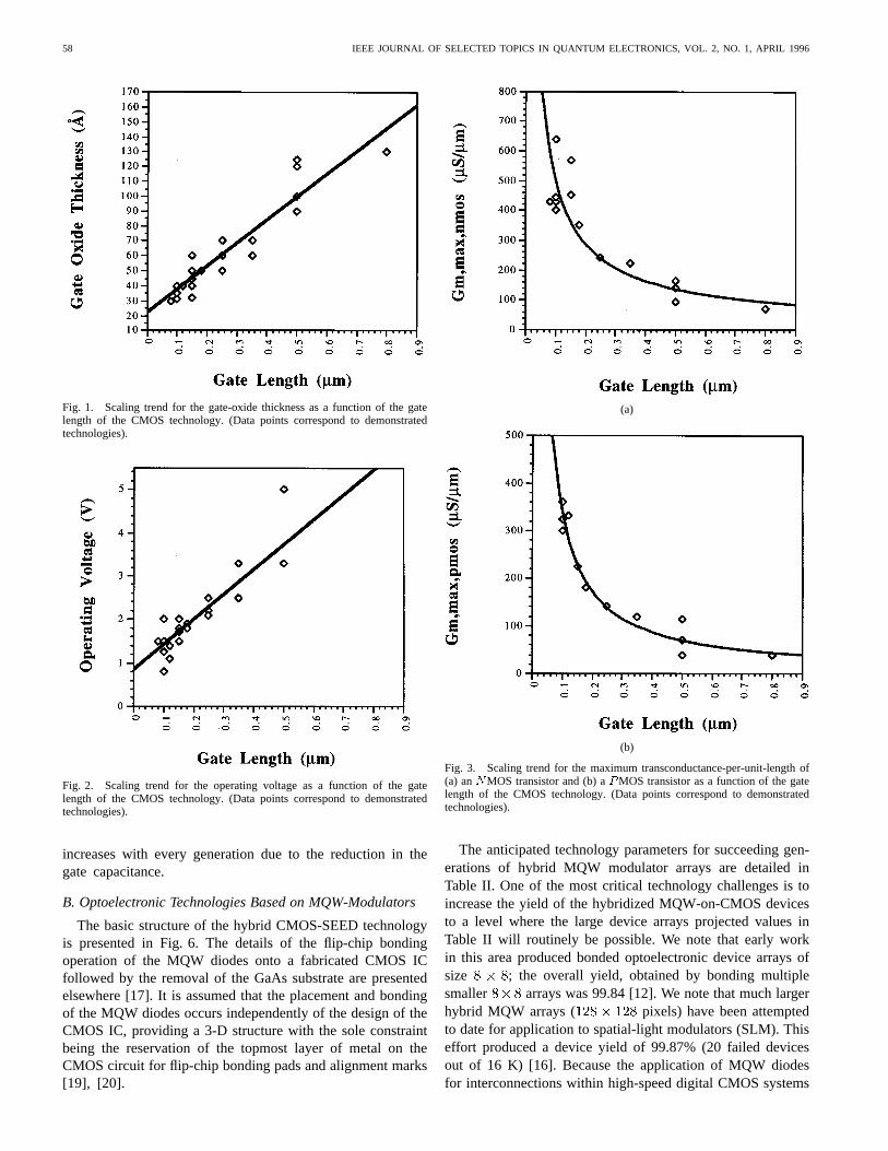
Figs. 1–5 show the empirical scaling of the gate oxidethickness, voltage, peak transconductance of theMOS and
MOSFET’s, nominal clock frequency of each technology,and the inverse gate-delay based on ring oscillator data. Asmentioned above, the threshold voltage of the FET’s is animportant parameter that affects the power-delay product ofthe gates. A higher ratio of the threshold voltageto thesupply voltage ) reduces the power dissipation of thecircuits but also increases their delay. It will be assumed thatthe ratio is maintained at about 1/4 to ensure adequateperformance improvement with each new generation [59]. Theempirical data suggests that the observed scaling is closer fit tothe quasi-constant voltage scaling model [60], [61], where thevoltage scales as approximately and the other parametersscale as . The resulting cutoff frequency, , of the FET’s
58 IEEE JOURNAL OF SELECTED TOPICS IN QUANTUM ELECTRONICS, VOL. 2, NO. 1, APRIL 1996
Fig. 1. Scaling trend for the gate-oxide thickness as a function of the gatelength of the CMOS technology. (Data points correspond to demonstratedtechnologies).
Fig. 2. Scaling trend for the operating voltage as a function of the gatelength of the CMOS technology. (Data points correspond to demonstratedtechnologies).
increases with every generation due to the reduction in thegate capacitance.
B. Optoelectronic Technologies Based on MQW-Modulators
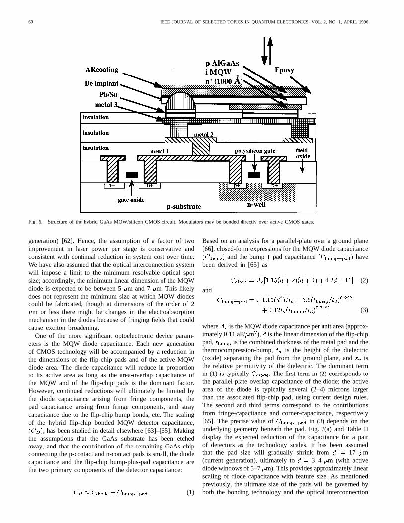
The basic structure of the hybrid CMOS-SEED technologyis presented in Fig. 6. The details of the flip-chip bondingoperation of the MQW diodes onto a fabricated CMOS ICfollowed by the removal of the GaAs substrate are presentedelsewhere [17]. It is assumed that the placement and bondingof the MQW diodes occurs independently of the design of theCMOS IC, providing a 3-D structure with the sole constraintbeing the reservation of the topmost layer of metal on theCMOS circuit for flip-chip bonding pads and alignment marks[19], [20].
(a)
(b)
Fig. 3. Scaling trend for the maximum transconductance-per-unit-length of(a) anNMOS transistor and (b) aPMOS transistor as a function of the gatelength of the CMOS technology. (Data points correspond to demonstratedtechnologies).
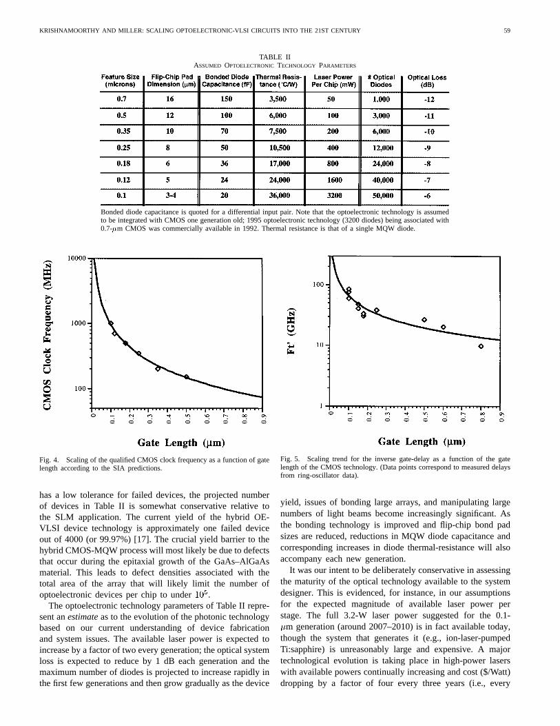
The anticipated technology parameters for succeeding gen-erations of hybrid MQW modulator arrays are detailed inTable II. One of the most critical technology challenges is toincrease the yield of the hybridized MQW-on-CMOS devicesto a level where the large device arrays projected values inTable II will routinely be possible. We note that early workin this area produced bonded optoelectronic device arrays ofsize ; the overall yield, obtained by bonding multiplesmaller arrays was 99.84 [12]. We note that much largerhybrid MQW arrays ( pixels) have been attemptedto date for application to spatial-light modulators (SLM). Thiseffort produced a device yield of 99.87% (20 failed devicesout of 16 K) [16]. Because the application of MQW diodesfor interconnections within high-speed digital CMOS systems
KRISHNAMOORTHY AND MILLER: SCALING OPTOELECTRONIC-VLSI CIRCUITS INTO THE 21ST CENTURY 59
TABLE IIASSUMED OPTOELECTRONIC TECHNOLOGY PARAMETERS
Bonded diode capacitance is quoted for a differential input pair. Note that the optoelectronic technology is assumedto be integrated with CMOS one generation old; 1995 optoelectronic technology (3200 diodes) being associated with0.7-�m CMOS was commercially available in 1992. Thermal resistance is that of a single MQW diode.
Fig. 4. Scaling of the qualified CMOS clock frequency as a function of gatelength according to the SIA predictions.
has a low tolerance for failed devices, the projected numberof devices in Table II is somewhat conservative relative tothe SLM application. The current yield of the hybrid OE-VLSI device technology is approximately one failed deviceout of 4000 (or 99.97%) [17]. The crucial yield barrier to thehybrid CMOS-MQW process will most likely be due to defectsthat occur during the epitaxial growth of the GaAs–AlGaAsmaterial. This leads to defect densities associated with thetotal area of the array that will likely limit the number ofoptoelectronic devices per chip to under .
The optoelectronic technology parameters of Table II repre-sent anestimateas to the evolution of the photonic technologybased on our current understanding of device fabricationand system issues. The available laser power is expected toincrease by a factor of two every generation; the optical systemloss is expected to reduce by 1 dB each generation and themaximum number of diodes is projected to increase rapidly inthe first few generations and then grow gradually as the device
Fig. 5. Scaling trend for the inverse gate-delay as a function of the gatelength of the CMOS technology. (Data points correspond to measured delaysfrom ring-oscillator data).
yield, issues of bonding large arrays, and manipulating largenumbers of light beams become increasingly significant. Asthe bonding technology is improved and flip-chip bond padsizes are reduced, reductions in MQW diode capacitance andcorresponding increases in diode thermal-resistance will alsoaccompany each new generation.
It was our intent to be deliberately conservative in assessingthe maturity of the optical technology available to the systemdesigner. This is evidenced, for instance, in our assumptionsfor the expected magnitude of available laser power perstage. The full 3.2-W laser power suggested for the 0.1-
m generation (around 2007–2010) is in fact available today,though the system that generates it (e.g., ion-laser-pumpedTi:sapphire) is unreasonably large and expensive. A majortechnological evolution is taking place in high-power laserswith available powers continually increasing and cost ($/Watt)dropping by a factor of four every three years (i.e., every
60 IEEE JOURNAL OF SELECTED TOPICS IN QUANTUM ELECTRONICS, VOL. 2, NO. 1, APRIL 1996
Fig. 6. Structure of the hybrid GaAs MQW/silicon CMOS circuit. Modulators may be bonded directly over active CMOS gates.
generation) [62]. Hence, the assumption of a factor of twoimprovement in laser power per stage is conservative andconsistent with continual reduction in system cost over time.We have also assumed that the optical interconnection systemwill impose a limit to the minimum resolvable optical spotsize; accordingly, the minimum linear dimension of the MQWdiode is expected to be between 5m and 7 m. This likelydoes not represent the minimum size at which MQW diodescould be fabricated, though at dimensions of the order of 2
m or less there might be changes in the electroabsorptionmechanism in the diodes because of fringing fields that couldcause exciton broadening.
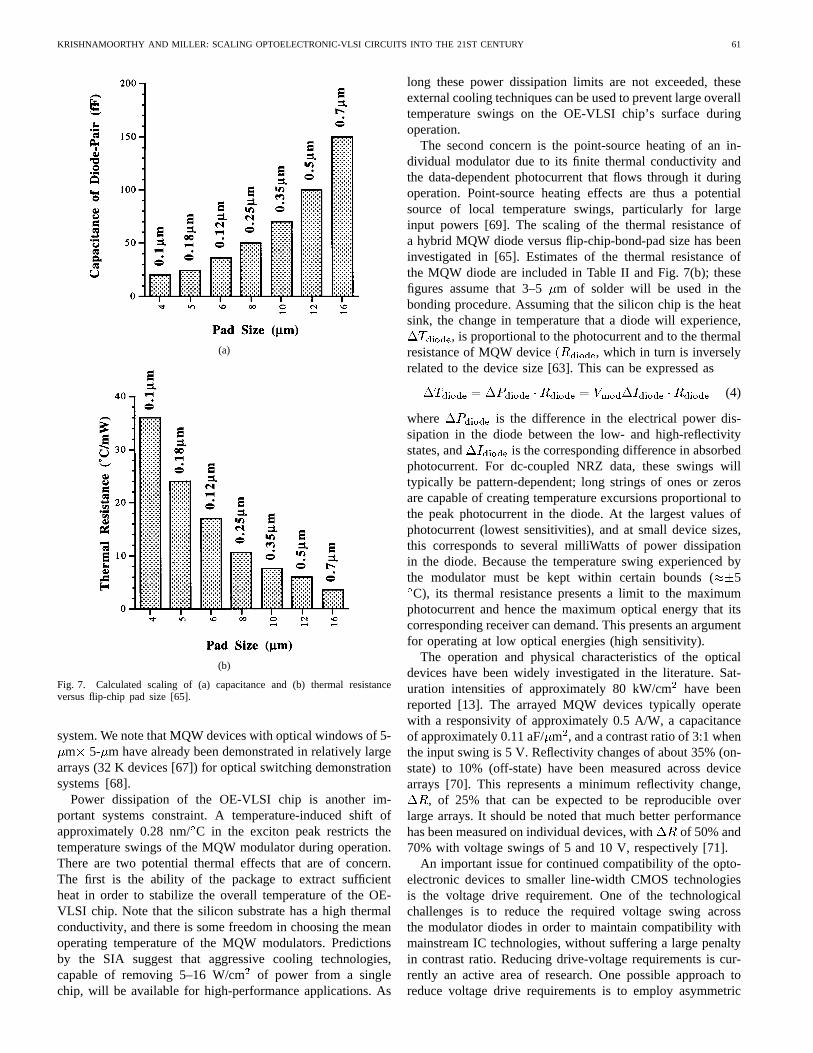
One of the more significant optoelectronic device param-eters is the MQW diode capacitance. Each new generationof CMOS technology will be accompanied by a reduction inthe dimensions of the flip-chip pads and of the active MQWdiode area. The diode capacitance will reduce in proportionto its active area as long as the area-overlap capacitance ofthe MQW and of the flip-chip pads is the dominant factor.However, continued reductions will ultimately be limited bythe diode capacitance arising from fringe components, thepad capacitance arising from fringe components, and straycapacitance due to the flip-chip bump bonds, etc. The scalingof the hybrid flip-chip bonded MQW detector capacitance,
, has been studied in detail elsewhere [63]–[65]. Makingthe assumptions that the GaAs substrate has been etchedaway, and that the contribution of the remaining GaAs chipconnecting the p-contact and n-contact pads is small, the diodecapacitance and the flip-chip bump-plus-pad capacitance arethe two primary components of the detector capacitance:
(1)
Based on an analysis for a parallel-plate over a ground plane[66], closed-form expressions for the MQW diode capacitance
and the bump pad capacitance havebeen derived in [65] as
(2)
and
(3)
where is the MQW diode capacitance per unit area (approx-imately 0.11 aF/m ), is the linear dimension of the flip-chippad, is the combined thickness of the metal pad and thethermocompression-bump, is the height of the dielectric(oxide) separating the pad from the ground plane, andisthe relative permittivity of the dielectric. The dominant termin (1) is typically . The first term in (2) corresponds tothe parallel-plate overlap capacitance of the diode; the activearea of the diode is typically several (2–4) microns largerthan the associated flip-chip pad, using current design rules.The second and third terms correspond to the contributionsfrom fringe-capacitance and corner-capacitance, respectively[65]. The precise value of in (3) depends on theunderlying geometry beneath the pad. Fig. 7(a) and Table IIdisplay the expected reduction of the capacitance for a pairof detectors as the technology scales. It has been assumedthat the pad size will gradually shrink from 17 m(current generation), ultimately to 3–4 m (with activediode windows of 5–7 m). This provides approximately linearscaling of diode capacitance with feature size. As mentionedpreviously, the ultimate size of the pads will be governed byboth the bonding technology and the optical interconnection
KRISHNAMOORTHY AND MILLER: SCALING OPTOELECTRONIC-VLSI CIRCUITS INTO THE 21ST CENTURY 61
(a)
(b)
Fig. 7. Calculated scaling of (a) capacitance and (b) thermal resistanceversus flip-chip pad size [65].
system. We note that MQW devices with optical windows of 5-m 5- m have already been demonstrated in relatively large
arrays (32 K devices [67]) for optical switching demonstrationsystems [68].
Power dissipation of the OE-VLSI chip is another im-portant systems constraint. A temperature-induced shift ofapproximately 0.28 nm/C in the exciton peak restricts thetemperature swings of the MQW modulator during operation.There are two potential thermal effects that are of concern.The first is the ability of the package to extract sufficientheat in order to stabilize the overall temperature of the OE-VLSI chip. Note that the silicon substrate has a high thermalconductivity, and there is some freedom in choosing the meanoperating temperature of the MQW modulators. Predictionsby the SIA suggest that aggressive cooling technologies,capable of removing 5–16 W/cmof power from a singlechip, will be available for high-performance applications. As
long these power dissipation limits are not exceeded, theseexternal cooling techniques can be used to prevent large overalltemperature swings on the OE-VLSI chip’s surface duringoperation.
The second concern is the point-source heating of an in-dividual modulator due to its finite thermal conductivity andthe data-dependent photocurrent that flows through it duringoperation. Point-source heating effects are thus a potentialsource of local temperature swings, particularly for largeinput powers [69]. The scaling of the thermal resistance ofa hybrid MQW diode versus flip-chip-bond-pad size has beeninvestigated in [65]. Estimates of the thermal resistance ofthe MQW diode are included in Table II and Fig. 7(b); thesefigures assume that 3–5m of solder will be used in thebonding procedure. Assuming that the silicon chip is the heatsink, the change in temperature that a diode will experience,
, is proportional to the photocurrent and to the thermalresistance of MQW device , which in turn is inverselyrelated to the device size [63]. This can be expressed as
(4)
where is the difference in the electrical power dis-sipation in the diode between the low- and high-reflectivitystates, and is the corresponding difference in absorbedphotocurrent. For dc-coupled NRZ data, these swings willtypically be pattern-dependent; long strings of ones or zerosare capable of creating temperature excursions proportional tothe peak photocurrent in the diode. At the largest values ofphotocurrent (lowest sensitivities), and at small device sizes,this corresponds to several milliWatts of power dissipationin the diode. Because the temperature swing experienced bythe modulator must be kept within certain bounds (5C), its thermal resistance presents a limit to the maximum
photocurrent and hence the maximum optical energy that itscorresponding receiver can demand. This presents an argumentfor operating at low optical energies (high sensitivity).
The operation and physical characteristics of the opticaldevices have been widely investigated in the literature. Sat-uration intensities of approximately 80 kW/cmhave beenreported [13]. The arrayed MQW devices typically operatewith a responsivity of approximately 0.5 A/W, a capacitanceof approximately 0.11 aF/m , and a contrast ratio of 3:1 whenthe input swing is 5 V. Reflectivity changes of about 35% (on-state) to 10% (off-state) have been measured across devicearrays [70]. This represents a minimum reflectivity change,
, of 25% that can be expected to be reproducible overlarge arrays. It should be noted that much better performancehas been measured on individual devices, with of 50% and70% with voltage swings of 5 and 10 V, respectively [71].
An important issue for continued compatibility of the opto-electronic devices to smaller line-width CMOS technologiesis the voltage drive requirement. One of the technologicalchallenges is to reduce the required voltage swing acrossthe modulator diodes in order to maintain compatibility withmainstream IC technologies, without suffering a large penaltyin contrast ratio. Reducing drive-voltage requirements is cur-rently an active area of research. One possible approach toreduce voltage drive requirements is to employ asymmetric
62 IEEE JOURNAL OF SELECTED TOPICS IN QUANTUM ELECTRONICS, VOL. 2, NO. 1, APRIL 1996
(a)
(b)
Fig. 8. Schematic of (a) single-ended (SE) optical interconnection link, (b)two-beam (TB) optical interconnection link;V
detandV
modare the detector
and transmitter bias voltages, respectively.�int
is the product of the opticalsystem power efficiency and the modulator power efficiency.
Fabry–Perot cavity structures [72]–[75]. The penalty is thereduced tolerance to device nonuniformity [76], [77]. Anothermethod is to use a stacked-diode modulator design that reducesdrive voltage at the expense of increased diode capacitance[71]. We will assume that the MQW design innovations suchas those described above will enable the technology to evolveaccording to Table II.
III. L IMITS ON THE NUMBER OF OPTICAL I/O CIRCUITS
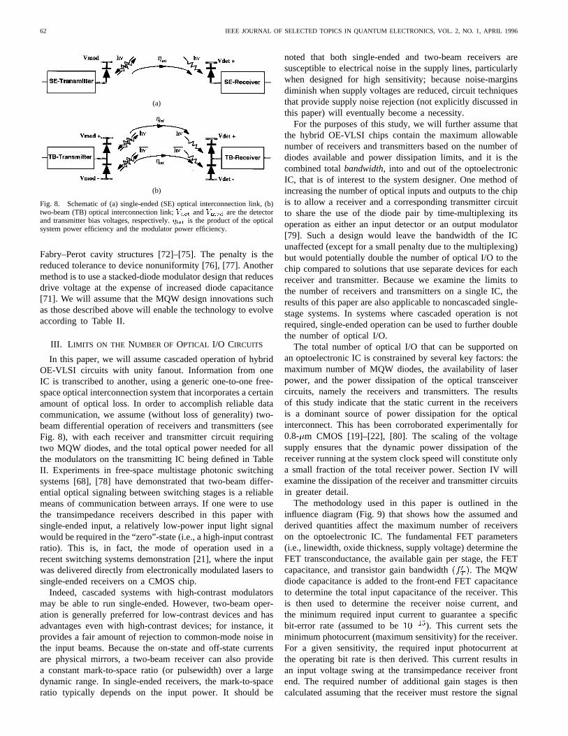
In this paper, we will assume cascaded operation of hybridOE-VLSI circuits with unity fanout. Information from oneIC is transcribed to another, using a generic one-to-one free-space optical interconnection system that incorporates a certainamount of optical loss. In order to accomplish reliable datacommunication, we assume (without loss of generality) two-beam differential operation of receivers and transmitters (seeFig. 8), with each receiver and transmitter circuit requiringtwo MQW diodes, and the total optical power needed for allthe modulators on the transmitting IC being defined in TableII. Experiments in free-space multistage photonic switchingsystems [68], [78] have demonstrated that two-beam differ-ential optical signaling between switching stages is a reliablemeans of communication between arrays. If one were to usethe transimpedance receivers described in this paper withsingle-ended input, a relatively low-power input light signalwould be required in the “zero”-state (i.e., a high-input contrastratio). This is, in fact, the mode of operation used in arecent switching systems demonstration [21], where the inputwas delivered directly from electronically modulated lasers tosingle-ended receivers on a CMOS chip.
Indeed, cascaded systems with high-contrast modulatorsmay be able to run single-ended. However, two-beam oper-ation is generally preferred for low-contrast devices and hasadvantages even with high-contrast devices; for instance, itprovides a fair amount of rejection to common-mode noise inthe input beams. Because the on-state and off-state currentsare physical mirrors, a two-beam receiver can also providea constant mark-to-space ratio (or pulsewidth) over a largedynamic range. In single-ended receivers, the mark-to-spaceratio typically depends on the input power. It should be
noted that both single-ended and two-beam receivers aresusceptible to electrical noise in the supply lines, particularlywhen designed for high sensitivity; because noise-marginsdiminish when supply voltages are reduced, circuit techniquesthat provide supply noise rejection (not explicitly discussed inthis paper) will eventually become a necessity.
For the purposes of this study, we will further assume thatthe hybrid OE-VLSI chips contain the maximum allowablenumber of receivers and transmitters based on the number ofdiodes available and power dissipation limits, and it is thecombined totalbandwidth, into and out of the optoelectronicIC, that is of interest to the system designer. One method ofincreasing the number of optical inputs and outputs to the chipis to allow a receiver and a corresponding transmitter circuitto share the use of the diode pair by time-multiplexing itsoperation as either an input detector or an output modulator[79]. Such a design would leave the bandwidth of the ICunaffected (except for a small penalty due to the multiplexing)but would potentially double the number of optical I/O to thechip compared to solutions that use separate devices for eachreceiver and transmitter. Because we examine the limits tothe number of receivers and transmitters on a single IC, theresults of this paper are also applicable to noncascaded single-stage systems. In systems where cascaded operation is notrequired, single-ended operation can be used to further doublethe number of optical I/O.
The total number of optical I/O that can be supported onan optoelectronic IC is constrained by several key factors: themaximum number of MQW diodes, the availability of laserpower, and the power dissipation of the optical transceivercircuits, namely the receivers and transmitters. The resultsof this study indicate that the static current in the receiversis a dominant source of power dissipation for the opticalinterconnect. This has been corroborated experimentally for0.8- m CMOS [19]–[22], [80]. The scaling of the voltagesupply ensures that the dynamic power dissipation of thereceiver running at the system clock speed will constitute onlya small fraction of the total receiver power. Section IV willexamine the dissipation of the receiver and transmitter circuitsin greater detail.
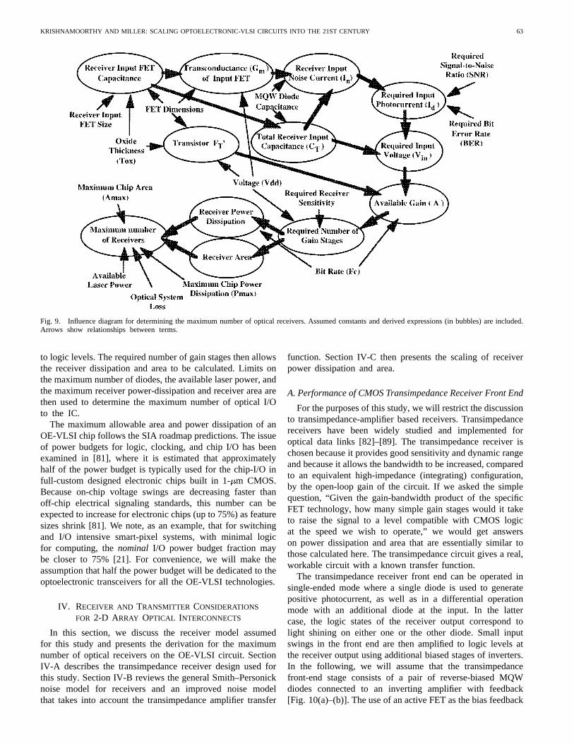
The methodology used in this paper is outlined in theinfluence diagram (Fig. 9) that shows how the assumed andderived quantities affect the maximum number of receiverson the optoelectronic IC. The fundamental FET parameters(i.e., linewidth, oxide thickness, supply voltage) determine theFET transconductance, the available gain per stage, the FETcapacitance, and transistor gain bandwidth . The MQWdiode capacitance is added to the front-end FET capacitanceto determine the total input capacitance of the receiver. Thisis then used to determine the receiver noise current, andthe minimum required input current to guarantee a specificbit-error rate (assumed to be ). This current sets theminimum photocurrent (maximum sensitivity) for the receiver.For a given sensitivity, the required input photocurrent atthe operating bit rate is then derived. This current results inan input voltage swing at the transimpedance receiver frontend. The required number of additional gain stages is thencalculated assuming that the receiver must restore the signal
KRISHNAMOORTHY AND MILLER: SCALING OPTOELECTRONIC-VLSI CIRCUITS INTO THE 21ST CENTURY 63
Fig. 9. Influence diagram for determining the maximum number of optical receivers. Assumed constants and derived expressions (in bubbles) are included.Arrows show relationships between terms.
to logic levels. The required number of gain stages then allowsthe receiver dissipation and area to be calculated. Limits onthe maximum number of diodes, the available laser power, andthe maximum receiver power-dissipation and receiver area arethen used to determine the maximum number of optical I/Oto the IC.
The maximum allowable area and power dissipation of anOE-VLSI chip follows the SIA roadmap predictions. The issueof power budgets for logic, clocking, and chip I/O has beenexamined in [81], where it is estimated that approximatelyhalf of the power budget is typically used for the chip-I/O infull-custom designed electronic chips built in 1-m CMOS.Because on-chip voltage swings are decreasing faster thanoff-chip electrical signaling standards, this number can beexpected to increase for electronic chips (up to 75%) as featuresizes shrink [81]. We note, as an example, that for switchingand I/O intensive smart-pixel systems, with minimal logicfor computing, thenominal I/O power budget fraction maybe closer to 75% [21]. For convenience, we will make theassumption that half the power budget will be dedicated to theoptoelectronic transceivers for all the OE-VLSI technologies.
IV. RECEIVER AND TRANSMITTER CONSIDERATIONS
FOR 2-D ARRAY OPTICAL INTERCONNECTS
In this section, we discuss the receiver model assumedfor this study and presents the derivation for the maximumnumber of optical receivers on the OE-VLSI circuit. SectionIV-A describes the transimpedance receiver design used forthis study. Section IV-B reviews the general Smith–Personicknoise model for receivers and an improved noise modelthat takes into account the transimpedance amplifier transfer
function. Section IV-C then presents the scaling of receiverpower dissipation and area.
A. Performance of CMOS Transimpedance Receiver Front End
For the purposes of this study, we will restrict the discussionto transimpedance-amplifier based receivers. Transimpedancereceivers have been widely studied and implemented foroptical data links [82]–[89]. The transimpedance receiver ischosen because it provides good sensitivity and dynamic rangeand because it allows the bandwidth to be increased, comparedto an equivalent high-impedance (integrating) configuration,by the open-loop gain of the circuit. If we asked the simplequestion, “Given the gain-bandwidth product of the specificFET technology, how many simple gain stages would it taketo raise the signal to a level compatible with CMOS logicat the speed we wish to operate,” we would get answerson power dissipation and area that are essentially similar tothose calculated here. The transimpedance circuit gives a real,workable circuit with a known transfer function.
The transimpedance receiver front end can be operated insingle-ended mode where a single diode is used to generatepositive photocurrent, as well as in a differential operationmode with an additional diode at the input. In the lattercase, the logic states of the receiver output correspond tolight shining on either one or the other diode. Small inputswings in the front end are then amplified to logic levels atthe receiver output using additional biased stages of inverters.In the following, we will assume that the transimpedancefront-end stage consists of a pair of reverse-biased MQWdiodes connected to an inverting amplifier with feedback[Fig. 10(a)–(b)]. The use of an active FET as the bias feedback
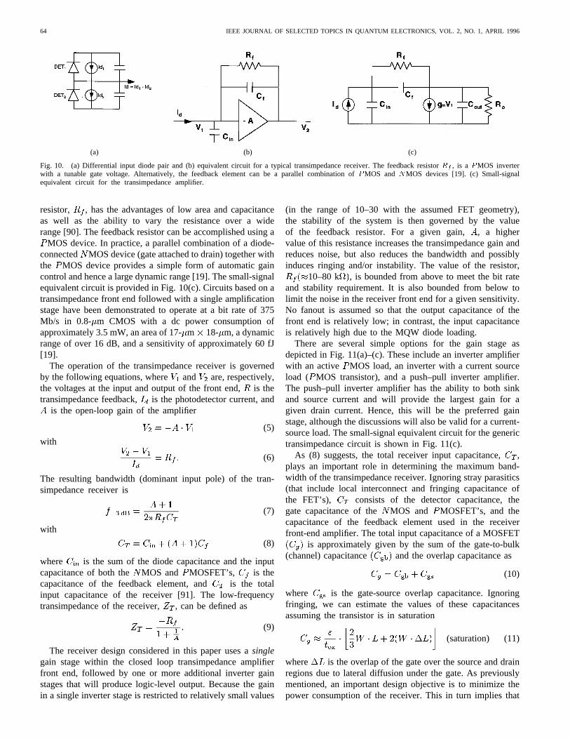
64 IEEE JOURNAL OF SELECTED TOPICS IN QUANTUM ELECTRONICS, VOL. 2, NO. 1, APRIL 1996
(a) (b) (c)
Fig. 10. (a) Differential input diode pair and (b) equivalent circuit for a typical transimpedance receiver. The feedback resistorRf , is a PMOS inverterwith a tunable gate voltage. Alternatively, the feedback element can be a parallel combination ofPMOS andNMOS devices [19]. (c) Small-signalequivalent circuit for the transimpedance amplifier.
resistor, , has the advantages of low area and capacitanceas well as the ability to vary the resistance over a widerange [90]. The feedback resistor can be accomplished using a
MOS device. In practice, a parallel combination of a diode-connected MOS device (gate attached to drain) together withthe MOS device provides a simple form of automatic gaincontrol and hence a large dynamic range [19]. The small-signalequivalent circuit is provided in Fig. 10(c). Circuits based on atransimpedance front end followed with a single amplificationstage have been demonstrated to operate at a bit rate of 375Mb/s in 0.8- m CMOS with a dc power consumption ofapproximately 3.5 mW, an area of 17-m 18- m, a dynamicrange of over 16 dB, and a sensitivity of approximately 60 fJ[19].
The operation of the transimpedance receiver is governedby the following equations, where and are, respectively,the voltages at the input and output of the front end,is thetransimpedance feedback, is the photodetector current, and
is the open-loop gain of the amplifier
(5)
with
(6)
The resulting bandwidth (dominant input pole) of the tran-simpedance receiver is
(7)
with
(8)
where is the sum of the diode capacitance and the inputcapacitance of both the MOS and MOSFET’s, is thecapacitance of the feedback element, and is the totalinput capacitance of the receiver [91]. The low-frequencytransimpedance of the receiver, , can be defined as
(9)
The receiver design considered in this paper uses asinglegain stage within the closed loop transimpedance amplifierfront end, followed by one or more additional inverter gainstages that will produce logic-level output. Because the gainin a single inverter stage is restricted to relatively small values
(in the range of 10–30 with the assumed FET geometry),the stability of the system is then governed by the valueof the feedback resistor. For a given gain,, a highervalue of this resistance increases the transimpedance gain andreduces noise, but also reduces the bandwidth and possiblyinduces ringing and/or instability. The value of the resistor,
10–80 k , is bounded from above to meet the bit rateand stability requirement. It is also bounded from below tolimit the noise in the receiver front end for a given sensitivity.No fanout is assumed so that the output capacitance of thefront end is relatively low; in contrast, the input capacitanceis relatively high due to the MQW diode loading.
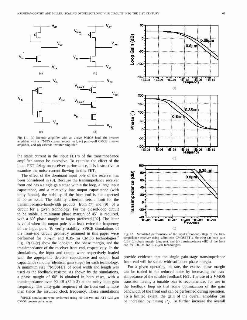
There are several simple options for the gain stage asdepicted in Fig. 11(a)–(c). These include an inverter amplifierwith an active MOS load, an inverter with a current sourceload ( MOS transistor), and a push–pull inverter amplifier.The push–pull inverter amplifier has the ability to both sinkand source current and will provide the largest gain for agiven drain current. Hence, this will be the preferred gainstage, although the discussions will also be valid for a current-source load. The small-signal equivalent circuit for the generictransimpedance circuit is shown in Fig. 11(c).
As (8) suggests, the total receiver input capacitance,,plays an important role in determining the maximum band-width of the transimpedance receiver. Ignoring stray parasitics(that include local interconnect and fringing capacitance ofthe FET’s), consists of the detector capacitance, thegate capacitance of the MOS and MOSFET’s, and thecapacitance of the feedback element used in the receiverfront-end amplifier. The total input capacitance of a MOSFET
is approximately given by the sum of the gate-to-bulk(channel) capacitance and the overlap capacitance as
(10)
where is the gate-source overlap capacitance. Ignoringfringing, we can estimate the values of these capacitancesassuming the transistor is in saturation
(saturation) (11)
where is the overlap of the gate over the source and drainregions due to lateral diffusion under the gate. As previouslymentioned, an important design objective is to minimize thepower consumption of the receiver. This in turn implies that
KRISHNAMOORTHY AND MILLER: SCALING OPTOELECTRONIC-VLSI CIRCUITS INTO THE 21ST CENTURY 65
(a) (b)
(c) (d)
Fig. 11. (a) Inverter amplifier with an activePMOS load, (b) inverteramplifier with aPMOS current source load, (c) push–pull CMOS inverteramplifier, and (d) cascode inverter amplifier.
the static current in the input FET’s of the transimpedanceamplifier cannot be excessive. To examine the effect of theinput FET sizing on receiver performance, it is instructive toexamine the noise current flowing in this FET.
The effect of the dominant input pole of the receiver hasbeen considered in (3). Because the transimpedance receiverfront end has a single gain stage within the loop, a large inputcapacitance, and a relatively low output capacitance (withunity fanout), the stability of the front end is not expectedto be an issue. The stability criterium sets a limit for thetransimpedance-bandwidth product [from (7) and (9)] of acircuit for a given technology. For the closed-loop circuitto be stable, a minimum phase margin of 45is required,with a 60 phase margin or larger preferred [92]. The latteris valid when the output pole is at least twice the frequencyof the input pole. To verify stability, SPICE simulations ofthe front-end circuit geometry assumed in this paper wereperformed for 0.8-m and 0.35- m CMOS technologies.2
Fig. 12(a)–(c) show the loopgain, the phase margin, and thetransimpedance of the receiver front end, respectively. In thesimulations, the input and output were respectively loadedwith the appropriate detector capacitance and output loadcapacitance (another identical gain stage) for each technology.A minimum size MOSFET of equal width and length wasused as the feedback resistor. As shown by the simulations,a phase margin of 60 is obtained in both cases, with atransimpedance over 90 dB (32 k) at the unity loop-gainfrequency. The unity-gain frequency of the front end is morethan twice the assumed clock frequency. These simulations
2SPICE simulations were performed using HP 0.8-�m and ATT 0.35-�mCMOS process parameters.
(a)
(b)
(c)
Fig. 12. Simulated performance of the input (front-end) stage of the tran-simpedance receiver using submicron CMOSFET’s, showing (a) loop gain(dB), (b) phase margin (degrees), and (c) transimpedance (dB) of the frontend for 0.8-�m and 0.35-�m technologies.
provide evidence that the single gain-stage transimpedancefront end will be stable with sufficient phase margin.
For a given operating bit rate, the excess phase margincan be traded in for reduced noise by increasing the tran-simpedance of the tunable feedback FET. The use of aMOStransistor having a tunable bias is recommended for use inthe feedback loop so that some optimization of the gainbandwidth of the front end can be performed during operation.To a limited extent, the gain of the overall amplifier canbe increased by tuning . To further increase the overall
66 IEEE JOURNAL OF SELECTED TOPICS IN QUANTUM ELECTRONICS, VOL. 2, NO. 1, APRIL 1996
gain of the receiver, additional inverter stages can be addedafter the transimpedance amplifier stage to increase the gain.The use of differential encoding together with appropriatetransistor sizing allows these further gain stages to be biased atthe midpoint . However, these additional gain stagesincrease the power dissipation of the receiver; this tradeoffwill be explored in the following sections. We have assumedthat these stages are effectively biased by the transimpedanceamplifier front end and calculate the static power dissipationof these additional stages based on this mid-point biasing.In practice, additional diode-connected FET’s can be usedbetween each pair of additional gain stages as resistor elementsto bias these stages; these additional resistors also broaden theoverall gain of each added stage and reduce the sensitivity ofthe receiver to input noise and process variations.
B. Receiver Front-End Noise Analysis
A generic receiver circuit is shown in Fig. 10(b). The noisebehavior of this circuit has been studied in [93], where it isshown that the total mean-square equivalent input noise due tothe input devices of the receiver (the photodiode, input FET,and bias resistor) front end has contributions arising from theJohnson noise of the bias resistor, the photodetector dark-current, the FET gate-leakage currents, the or “flicker”noise in the FET’s, and the channel noise of the input FET[89], [91], [93]:
(12)
where is the cutoff bit rate, is the sum of the photodiodeand FET leakage currents, , and are the normalizedPersonick noise bandwidth integrals, respectively,is theelectron charge constant, is the noise corner frequency,and is the excess channel noise factor term associated withshort-channel transistors. The basic formula for noise in (12)applies to any receiver design; it can be verified from thefundamental noise mechanisms in the devices by ignoring theconstants ( , and ), assuming a very simple model ofbiased gain stages without feedback, and replacing the cutoffbit rate, , by the bandwidth.
The or flicker noise in CMOSFET’s is a result offluctuations in the number of trapped carriers in the gate oxidenear the MOS interface. Typical flicker noise corner frequen-cies for MOSFET’s are on the order of a few megahertz.There is evidence that noise will increase in short-channelFET’s, as hot carriers degrade the channel [94], [95]. Although
noise may become potentially disastrous in terms ofhigh-sensitivity (dc-coupled) receiver performance, the use ofencoding techniques to remove the low-frequency componentsin the data stream can be an effective means to amelioratethis potential problem. It should be noted that ac-coupleddata encoding will also reduce point-source heating effectsin the modulators and may ultimately prove quite valuable forOE-VLSI systems integration.
The precise expression given in (12) and the calculation ofthe Personick integrals, , and , are strictly valid only fora family of rectangular input pulses and a raised cosine outputpulses in a linear, equalized channel that is filtered prior to thedecision circuit. According to the Smith–Personick analysis,the values of and are relatively insensitive to the fractionof the time slot occupied by the pulse, or to the exact shapeof the raised cosine pulse, i.e.,over a wide range of parameters. But in order to estimate thenoise, we would be required to assume that the receiver has acutoff frequency, , exactly equal to the operating bit rate,
. Furthermore, we would also be required to assume thatthe output waveform at this bit rate has the shape of a raisedcosine. Most practical receivers, such as the one consideredin this paper, instead employ NRZ input and output pulseswithout equalizer stages or a well-defined cutoff bit rate.
The interpretation of the Smith–Personick analysis has beenaddressed more carefully in [96] where the noise perfor-mance of an unequalized transimpedance receiver has beenconsidered without making assumptions on the input/outputpulse shapes. Indeed, their results verify that the use of theSmith–Personick analysis, without regard to the points men-tioned above, can lead to a significant underestimation of therms noise current. Hence, it is important to consider the effectof the transfer function of the specific receiver front end whenperforming the noise calculation. While these refinements willbe valid only for transimpedance front ends, they providea more accurate estimate of the expected sensitivity of thereceivers.
From [96], the mean square input noise current for atransimpedance receiver [Fig. 10(b)] can be written as
(13)
where
(14)
and where is defined as (15), shown at the bottom of thenext page. is the total input capacitance of the receiverfrom (8), and is the output resistance of the front-end inverter amplifier. The input , output , andfeedback capacitance in (14) and (15) for a two-beaminverter-amplifier-based receiver are given by
(16)
(17)
(18)
where is the load capacitance of the following stage(consisting of an identical inverter amplifier). The feedbackcapacitance in (18) includes the drain-source capacitance of thefeedback FET and the gate-drain capacitances (in brackets) ofthe MOS and MOSFET’s in the inverter amplifier. From(8), we see that these last two terms in (18) are multiplied by
KRISHNAMOORTHY AND MILLER: SCALING OPTOELECTRONIC-VLSI CIRCUITS INTO THE 21ST CENTURY 67
the gain of the amplifier, due to the Miller effect. One methodof eliminating this Miller capacitance is to use a cascodeamplifier configuration [Fig. 11(d)] [92]. The second term in(12) and (13) represents shot noise contributions of the diodedark current and FET leakage for nonreturn-to-zero coded data.Photodiode dark currents for the hybrid MQW modulators areexpected to be on the order of a few nanoamperes or less.The FET leakage is directly related to the threshold voltageof the FET’s. Low threshold voltages directly result in highsubthreshold conduction and leakage currents in the FET’s.Due to the exponential nature of the subthreshold current, thethreshold voltage cannot typically be scaled down linearlywith feature size. Higher leakage currents will have detrimentaleffects on the performance of the analog circuits and willalso increase the overall static power dissipation of the chip[24]–[31], [61]. The expression for subthreshold conductionof a FET, , can be written as
(19)
where is the subthreshold conduction slope of the submicronMOSFET (defined as the change in gate voltage required toinduce a change in drain current), and is the draincurrent of the FET at the onset of saturation. is on theorder of 100 nA multiplied by the width-to-lengthratio of the FET. We will assume that the subthreshold slopewill be 80 mV/decade or below, which is consistent with theexpected performance of deep submicron MOSFET’s at roomtemperature. As mentioned in Section II-A, a ratio ofapproximately four will be assumed in this paper. While FETleakage currents of 1–10 pA/m are expected for the longerchannel devices, an evaluation of (19) suggests that very shortchannel transistors (0.1m) may exhibit leakage currents onthe order 100 pA–1 nA. Even at these levels, the overall effectof the leakage current on the receiver noise is small.
The significant sources of input noise are the first and lastterms in (12) and (13). The first term is due to the thermal noisein the feedback resistor used in the transimpedance amplifier;for the high-resistance (e.g., 40 k ) FET-based feedbackresistor, this term is typically small; it dominates only when
10 k . As a result, the dominant term for wide-bandwidth receivers is the last term, corresponding to themean-square input-noise current due to the channel (Johnson)noise in the input FET. Notice that this noise current isinversely proportional to the transconductance of the input-stage FET and directly proportional to the square of thetotal input capacitance of the receiver front end. A smallerFET in the front end also has lower capacitance, but thetransconductance of the FET is proportionately reduced whenits dimensions are shrunk. The conventional wisdom is toincrease the transconductance of the FET (by optimizing itswidth-to-length ratio) to the point where the capacitance of
the input FET is equal to the detector capacitance (plus thefeedback capacitance). It can be shown that the optimumnoise current is obtained when this occurs [89], [91], [93].This maximizes the gain bandwidth of the front-end amplifierand minimizes the well-known figure-of-merit of the receiver,
, where is the front-end-inverter transconduc-tance and the total input capacitance. This is typicallydone in telecommunications receivers [97], where the primaryobjective is to maximize the sensitivity of the receiver andhence to reduce the noise current to a minimum. However,the resulting input FET (for a current-source load) is typicallylarge, resulting in large static current, and hence this sensitivityperformance can result in unacceptably high power consump-tion per receiver. It was recently pointed out in [98] that theinput FET capacitance could be reduced to approximately 20%of the sum of the photodetector capacitance plus the straycapacitance due to the feedback FET, without a significantchange in the overall noise of the receiver. In this paper, wesuggest further reductions in the input capacitance (comparedto the photodetector capacitance) for arrays of receivers; thisleads to a significant reduction in power dissipation in thereceiver array, with only a small added noise penalty.
For large arrays of (smart-pixel) receivers, a general conclu-sion follows that the FET technology cannot be exercised soas to obtain true noise-limited receiver sensitivity. The smartpixel receivers discussed here will typically be gain-limited atthe given bit rates due to the need for low power consumption.The addition of gain stages can improve the sensitivity up tothe noise limit. To see this, one can write the low-frequencygain of an inverter as
(20)
From (20), one can see that the small-signal gain of theCMOS inverter amplifier is limited by its own output con-ductance. Typical open-loop inverter-gains are in the rangeof 10–30. Hence, at the highest quoted sensitivities, a singletransimpedance gain stage will not be sufficient to producethe voltage swings necessary for a receiver decision stage toreliably restore to logic levels. To reduce the required swingat the input (and hence improve the sensitivity), additionalstages of inverter amplifiers or gain-broadened inverters canbe used in the front end. This allows smaller input pho-tocurrents without reducing the bandwidth of the receiver.In this paper, the assumed geometry for the transimpedancefront-end amplifier with push–pull inverter amplifiers, will bean MOS transistor three times the minimum size inseries with a MOS transistor approximately nine times theminimum geometry . This would provide approximatelysimilar transconductances for theMOS and MOSFET’s(and hence similar noise performance). Receivers that use thisfront-end geometry have been fabricated and tested in 0.8-
(15)
68 IEEE JOURNAL OF SELECTED TOPICS IN QUANTUM ELECTRONICS, VOL. 2, NO. 1, APRIL 1996
m CMOS and show reasonable bandwidth and sensitivity[19]–[21].
As the feature size and gate length of the FET technology isscaled down, the input capacitance of the FET’s that constitutethe receiver front end will proportionately decrease. Becausewe have assumed a constant geometry (in terms of the gatelength) for the front-end amplifier stage, the total receiver inputcapacitance will always be dominated by the capacitance of theMQW diode pair (quoted in Table II). Because we also assumethat the MQW diode capacitance is scaled down with theCMOS feature size, the overall effect is that the contributionof the input FET’s is between 5–15% of the total receiverinput capacitance throughout the scaling.
The excess channel noise factor,, is typically quoted as aconstant for receiver noise calculations in a given technology(e.g., for 1- m gate-length FET’s [91]). The scalingof this noise factor in submicron MOSFET’s has been studiedin greater detail in [99]–[101]. The exact value ofdependson the precise biasing and transconductance value of the FET.The noise factor is higher when the FET enters saturation;this is likely caused by hot electron effects in the pinched-off (high-field) part of the channel. As the FET linewidthis reduced below 1 m, the studies indicate that the noisefactor in submicron MOSFET’s can be significantly higher(by a factor of two to four) than that ideal value ofpredicted by long-channel theory [100]. For the receiver frontend considered in this paper, we include a linear scaling ofwith gate length, ranging from to , to accountfor this increased channel noise as the device size is reduced.These values are consistent with empirically observed behaviorin submicron FET’s down to 0.25-m gate lengths [99].
Because the excess channel noise factor of the FET is afunction of technology scaling (noise factor increases as thelinewidth is reduced), we can rewrite the noise figure-of-meritfrom (5) and (6) to , where is the excesschannel noise factor. If we make the further assumptions thatthe capacitance of the input FET’s is a known fraction of thedetector capacitance, , and that the feedback capacitance isnot significant, then we can further refine this figure-of-meritby substituting the expression for the unity-gain frequency
of the FET’s [102] as
(21)
Equation (21) permits the figure-of-merit for the sensitivity ofthe receiver to be simplified to , which representsthe performance of the specific OE-VLSI technology in termsof the detector capacitance, the unity-gain bandwidth of theFET’s, and the channel noise factor of the FET’s. Thisfigure-of-merit provides an indication of the improvementin receiver performance that we may expect as the OE-VLSI technology is scaled. The extent to which the actualreceiver sensitivity will track this technology figure-of-merit(assuming the technology scales are as expected) depends uponlimits placed on the specific receiver circuit, including powerdissipation constraints, and area.
The noise current can be calculated from (13)–(15), wherethe transconductance is given by [103]
saturation
(22)
where is the channel-length modulation parameter; second-order effects due to gate electric field and source-drain electricfields have been neglected. Empirical data and trend linesfor the saturation transconductance of bothMOS’s and
MOSFET’s are shown in Fig. 3(a)–(b). Equations (12)–(14)determine the minimum input current required to achieve therequisite bit-error rate (BER). In calculating the noise limitedreceiver input current, it has been assumed that thenoisesource associated with CMOS circuits could be neglected(or otherwise circumvented, for instance, by appropriate data-encoding). As previously mentioned, the receivers in an arrayare typically operated well above the noise-limited regime, sothat the input photocurrent obeys the condition fora BER of . Differential signaling is assumed so that thephotocurrent swing is doubled to a factor of 16 larger than therms noise current. For a given input current at the operating bitrate (or switching energy), the effective input voltage swing
can be written as
(23)
where is the bit duration. The output voltage of thereceiver front end can then be calculated from (5) asa function of the gain of the amplifier.
The sensitivity of the receiver can be expressed as either anoptical power required at the given bit rate (in dBm) or as anoptical energy/bit required at the receiver for the givenbit rate. For receivers with electronic gain, will typicallybe dependent on the bit rate. The optical energy required perbit can be expressed as a function of the average optical powerin the beam, the fraction of time that the light is present duringthe received data stream, and the bit period as [104]
(24)
where is the average optical power in the input beamthat will guarantee a specific bit-error rate, is the numberof transmitted bits, is the number of light pulses, andis the bit period. in (24) can be replaced by , where
is the average photocurrent in the receiver, andis theresponsivity of the detector. For random NRZ data with single-ended receivers, the ratio is equal to two, and isthe inverse of the operating bit rate. For NRZ data withtwo-beam, differential receivers, the ratio per detectoris equal to two, and an effective per beam can be defined.It will be the convention in this paper to quote the energyperbeam when calculating sensitivities.
C. Scalability of OE-VLSI Transceiver Circuits
Given the requirements for the input photocurrent in thereceivers, we can calculate the number of cascaded am-plifier (inverter) stages at the given bandwidth needed to
KRISHNAMOORTHY AND MILLER: SCALING OPTOELECTRONIC-VLSI CIRCUITS INTO THE 21ST CENTURY 69
produce the full logic swing at the output of the receiver.This will determine the overall power dissipation and areaof the receiver circuit. The transistor calculated in (21)is a small-signal parameter corresponding to unity currentgain bandwidth (whereas we are using a voltage amplifier).The unity voltage-gain frequency of a series of identicalcascaded inverter stages, denoted by, represents the highestfrequency at which gain can be extracted from the inverter[105]; this is typically layout-dependent and difficult to expressin closed form. However, it can be approximated by thegate delay of the technology as determined by ring-oscillatorfrequency measurements (Fig. 5); this empirical data alsocaptures the effect of parasitic interconnect capacitances. Fromthis data, the gain available from one stage of the amplifier canbe calculated. The logarithm of the ratio of the voltage swingrequired at the receiver output to the effective inputvoltage swing from (23), taken to the base of the gain availablefrom one such amplifier stage, represents the number of suchstages that will be needed in the receiver front end. The totalpower dissipation of the receiver follows from the dissipationper stage and the number of required stages, the latter growinglogarithmically with reducing receiver input energy. A similarscaling applies for the receiver area.
We assume that the receiver front end is biased in itssaturation region at approximately half the supply voltage. Thestatic power dissipation of the two-beam receiver with a singlebiased input stage can be calculated from
(25)
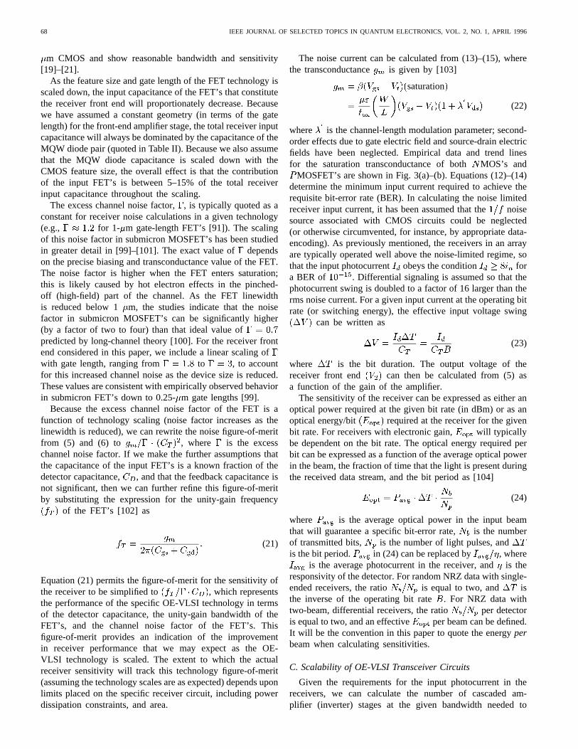
where is the current flowing through the biased tran-simpedance input stage. Equation (25) is valid for current-source load or for a push–pull inverter biased to allow thedrain-source currents in the MOS and MOS devices tobe equal. Making the simplifying assumption that the current-gain factors and the absolute thresholds are equal forboth MOS and MOS devices, this allows the inverter to bebiased at . Note that this expression applies only whenthe circuit is in its quiescent state. Once the receiver switchesto a stable state corresponding to a received bit, this staticpower dissipation component reduces due to a small excursionfrom its quiescent bias point; the corresponding dynamicpower dissipation of the receiver circuit increases according tothe bit rate. At the operating bit rates assumed in this paper, thedominant source of the receiver power dissipation is the largestatic current; the worst-case power dissipation is thus dictatedby (25). Fig. 13 shows the receiver power dissipation versusoptical energy required at the receiver. For a specific linewidthtechnology, there is a tradeoff between the optical energy-per-bit (or sensitivity) required by a receiver and its electricalpower dissipation. Reducing the optical energy (increasing thesensitivity) results in a lower input voltage swing . Thiscan be compensated by increasing the gain in the receiver,which leads to a larger number of gain stages and hence ahigher power dissipation. The calculated data points representan integer number of gain stages in the receiver for the givenfront-end FET geometries; the front-end FET’s can be changedto allow different values of gain. The calculated data points
Fig. 13. Receiver power dissipation versus optical energy-per-bit required atreceiver. Receiver noise limits represent an operating BER of10
�15.
Fig. 14. Receiver area versus optical energy-per-bit required at receiver.
as well as a logarithmic fit to the data (representing differentvalues of gain per stage) have been plotted.
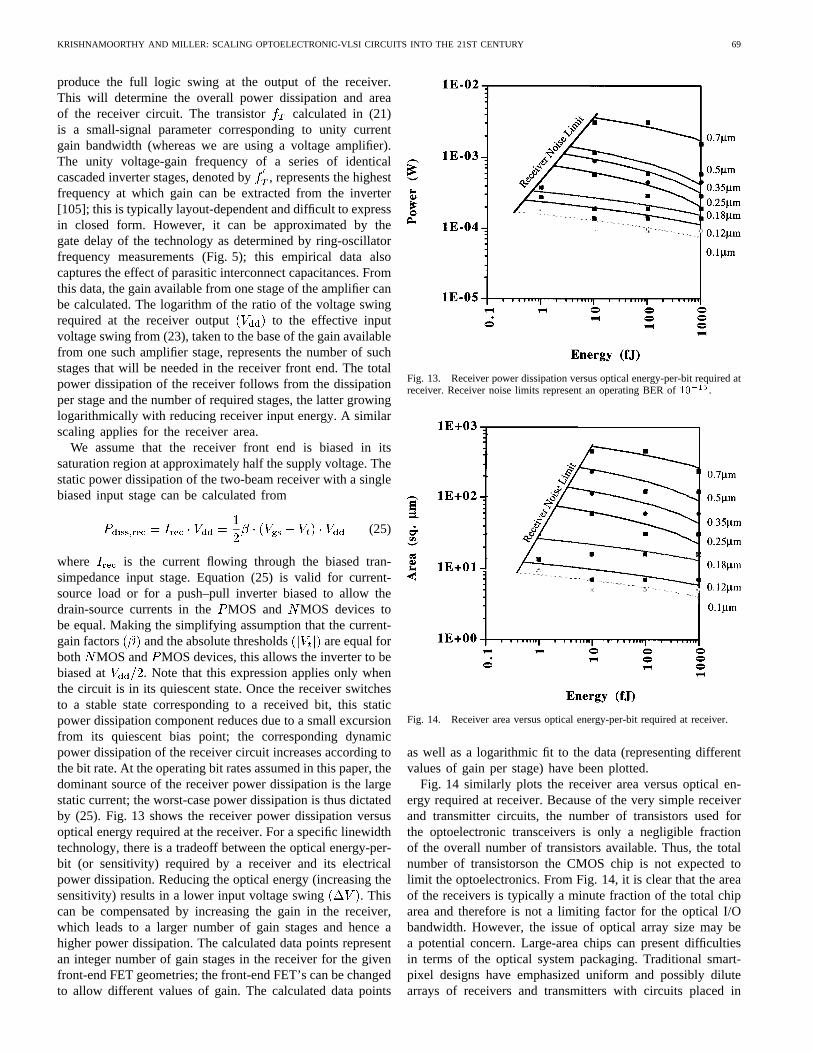
Fig. 14 similarly plots the receiver area versus optical en-ergy required at receiver. Because of the very simple receiverand transmitter circuits, the number of transistors used forthe optoelectronic transceivers is only a negligible fractionof the overall number of transistors available. Thus, the totalnumber of transistorson the CMOS chip is not expected tolimit the optoelectronics. From Fig. 14, it is clear that the areaof the receivers is typically a minute fraction of the total chiparea and therefore is not a limiting factor for the optical I/Obandwidth. However, the issue of optical array size may bea potential concern. Large-area chips can present difficultiesin terms of the optical system packaging. Traditional smart-pixel designs have emphasized uniform and possibly dilutearrays of receivers and transmitters with circuits placed in
70 IEEE JOURNAL OF SELECTED TOPICS IN QUANTUM ELECTRONICS, VOL. 2, NO. 1, APRIL 1996
close proximity to their receivers and transmitters. These andother design choices, optimized for the optical interconnectionsystem, are also possible since there are few restrictions in theplacement of the optical diodes with respect to the underlyingCMOS circuits.
We note that the use of optical interconnects can promotea specific technology to operate at bit rates well beyond thequalified speed of the technology given in Table I. Experimentsin 0.8- m CMOS technology have demonstrated the ability tooperate receiver and transmitter circuits beyond 500 MHz (1Gb/s NRZ data [22]), which is over five times the qualifiedclock frequency of the CMOS technology. This frequency isapproximately , where is the reciprocal gate delay.When operating at such high bit rates, the dynamic switchingin the tranceivers will lead to significant power consumption.However, the opportunity exists to reduce the number oftranceivers on the chip in favor of a higher bit rate per link,while keeping the overall optical I/O bandwidth to the chipconstant. Dynamic power dissipation data versus bit rate foran experimental 0.8-m CMOS receiver and transmitter areprovided in [80].
The transmitter (modulator) driver circuits will also con-sume a fraction of the total power budget. Driver circuitsfor the hybrid MQW modulators are typically comprised of asimple inverter buffer sized to drive the modulator capacitanceand sink the photocurrent absorbed in the low-reflectivity stateof the modulator [106], [107]. The modulator driver circuitpower dissipation (assuming a two-beam transmitter) can bewritten as
(26)
where
(27)
where is the total transmitter capacitance to be switched(including driver capacitance), is the peak photocurrentrequired in the following detector, and is the voltagedifference (bias) across the modulator in its highly absorbingstate. is the product of the optical system link efficiency
, and the modulator efficiency , given by thereflectivity difference between its two operating states:
(28)
where and are, respectively, the fractions ofthe optical input power that are available in the correspondinghigh and low reflectivity output states of the modulator. Notethat the modulator efficiency includes the effect of the insertionloss and the finite contrast ratio of the modulator device. It isassumed that the voltage swing across the modulators is thesupply voltage, , and that the bias voltage , across theabsorbing diode in the transmitter circuit is twice the supplyvoltage. The second term in (26) reflects the fact that halfthe combined input power to both diodes of a differentialtransmitter is always being absorbed, regardless of the bitpattern. For single-ended transmitters, (26) is valid when
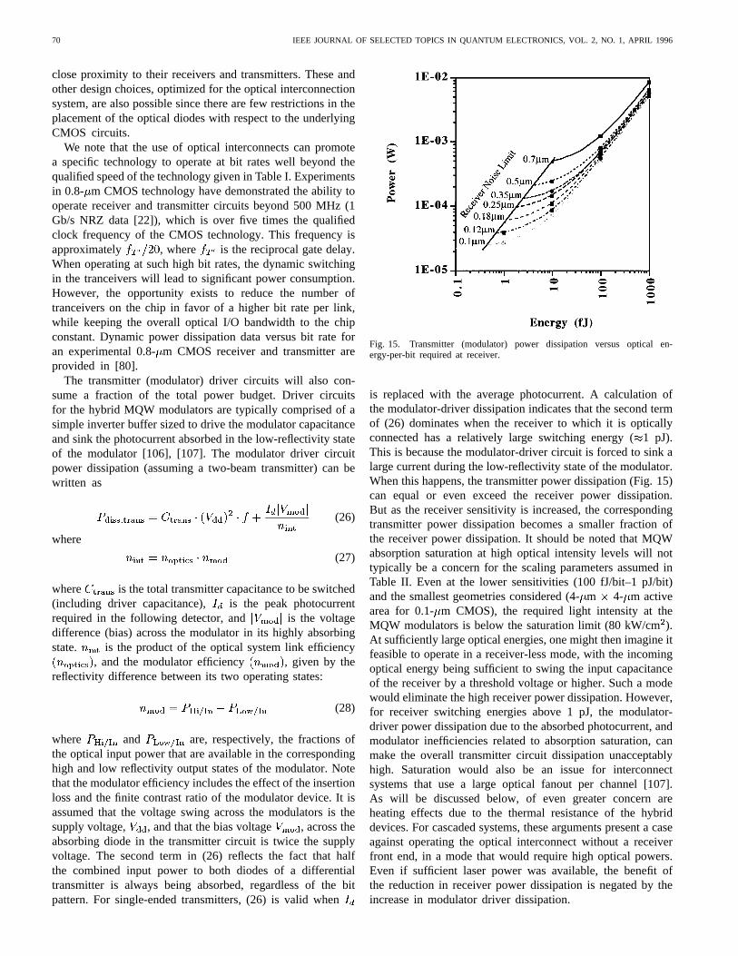
Fig. 15. Transmitter (modulator) power dissipation versus optical en-ergy-per-bit required at receiver.
is replaced with the average photocurrent. A calculation ofthe modulator-driver dissipation indicates that the second termof (26) dominates when the receiver to which it is opticallyconnected has a relatively large switching energy (1 pJ).This is because the modulator-driver circuit is forced to sink alarge current during the low-reflectivity state of the modulator.When this happens, the transmitter power dissipation (Fig. 15)can equal or even exceed the receiver power dissipation.But as the receiver sensitivity is increased, the correspondingtransmitter power dissipation becomes a smaller fraction ofthe receiver power dissipation. It should be noted that MQWabsorption saturation at high optical intensity levels will nottypically be a concern for the scaling parameters assumed inTable II. Even at the lower sensitivities (100 fJ/bit–1 pJ/bit)and the smallest geometries considered (4-m 4- m activearea for 0.1- m CMOS), the required light intensity at theMQW modulators is below the saturation limit (80 kW/cm).At sufficiently large optical energies, one might then imagine itfeasible to operate in a receiver-less mode, with the incomingoptical energy being sufficient to swing the input capacitanceof the receiver by a threshold voltage or higher. Such a modewould eliminate the high receiver power dissipation. However,for receiver switching energies above 1 pJ, the modulator-driver power dissipation due to the absorbed photocurrent, andmodulator inefficiencies related to absorption saturation, canmake the overall transmitter circuit dissipation unacceptablyhigh. Saturation would also be an issue for interconnectsystems that use a large optical fanout per channel [107].As will be discussed below, of even greater concern areheating effects due to the thermal resistance of the hybriddevices. For cascaded systems, these arguments present a caseagainst operating the optical interconnect without a receiverfront end, in a mode that would require high optical powers.Even if sufficient laser power was available, the benefit ofthe reduction in receiver power dissipation is negated by theincrease in modulator driver dissipation.
KRISHNAMOORTHY AND MILLER: SCALING OPTOELECTRONIC-VLSI CIRCUITS INTO THE 21ST CENTURY 71
Fig. 16. Maximum number of receivers that can be supported on an IC ver-sus optical energy required at individual receiver. Receiver power dissipationand optical power limit the total number of receivers. Circuit noise limitsand diode thermal limits constrain the sensitivity of each receiver. Curves areshown only for 0.7-�m, 0.35-�m, 0.18-�m, and 0.1-�m technologies.
V. GRAIN-SIZE COMPLEXITY AND I/O BANDWIDTH
LIMITS FOR OPTOELECTRONIC-VLSI CIRCUITS
Assuming two IC’s populated with modulator-drivers andreceivers, respectively, (or IC’s containing both modulator-drivers and receivers and sharing the use of the diode array),the aggregate I/O bandwidth to the chip will primarily belimited by: 1) area and power consumption of the receivers;2) the availability of sufficient laser power to interrogate themodulators on the transmitting IC and transmit the informationto their corresponding receivers on the receiving IC; and 3) thetotal number of optical diodes available. We will focus first onthe maximum number of receivers that can be supported onan optoelectronic IC.
The limit on the number of receivers that can be accom-modated on a single IC can be determined from (25) and(26), assuming that the total power dissipation budget is given(Table I) and that 50% of the budget may be used for theoptical transceivers.
Fig. 16 shows the tradeoff between the maximum numberof receivers on an optoelectronic IC and the optical energyrequired to switch each receiver in a cascaded system, as-suming up to 50% of the available power budget (from TableI) can be spent on I/O to the chip. Limits due to receiverpower dissipation and due to optical power limits (diagonallines) are shown for 0.7 m, 0.35 m, 0.18 m, and 0.1 mtechnologies, respectively. All receivers on an OE-VLSI chipare assumed to be identical. As the figure indicates, the powerdissipation of the receiver versus its optical input switchingenergy can be optimized in order to maximize the number ofoptical I/O to the IC. A useful conclusion is that a carefuloptimization of receiver power dissipation versus sensitivityis an important part of the system design. This is especiallytrue in the earlier CMOS generations as well as in situations
Fig. 17. Limits on the number of optical I/O devices and gates-per-I/Odevice that may be supported on the OE-VLSI chip. Sloping lines representVLSI limits, while vertical lines correspond to OE limits. Curves are shownonly for 0.7-�m, 0.35-�m, 0.18-�m, and 0.1-�m technologies.
where advanced cooling techniques cannot be used, and theacceptable power dissipation (and therefore the number ofreceivers) may differ from the values assumed in Table I.
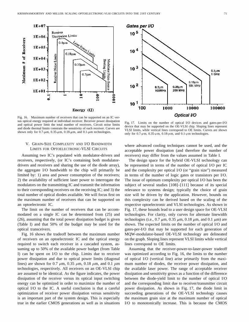
The design space for the hybrid OE-VLSI technology canbe represented in terms of the number of optical I/O per ICand the complexity per optical I/O (or “grain size”) measuredin terms of the number of logic gates or transistors per I/O.The issue of optimum complexity per optical I/O has been thesubject of several studies [108]–[111] because of its specialrelevance to systems design; typically the choice of grainsize will be driven by the application. However, bounds onthis complexity can be derived based on the scaling of therespective optoelectronic and VLSI technologies. As shown inFig. 17, these bounds lead to a user design space for OE-VLSItechnologies. For clarity, only curves for alternate linewidthtechnologies (i.e., 0.7m, 0.35 m, 0.18 m, and 0.1 m) areshown. The expected limits on the number of optical I/O andgates-per-I/O that may be supported for each generation ofMQW-modulator-based OE-VLSI technology are delineatedon the graph. Sloping lines represent VLSI limits while verticallines correspond to OE limits.
Assuming that the receiver-power-to-laser-power tradeoffwas optimized according to Fig. 16, the limits to the numberof optical I/O (vertical line) arise primarily from the maxi-mum number of diodes, the receiver power dissipation, andthe available laser power. The range of acceptable receiverdissipation and sensitivity grows as a function of the differencebetween the diode-yield limit to the number of optical I/Oand the corresponding limit due to receiver/transmitter circuitpower dissipation. As shown in Fig. 17, the diode limit insucceeding generations of the OE-VLSI technology causesthe maximum grain size at the maximum number of opticalI/O to monotonically increase. This is because the CMOS
72 IEEE JOURNAL OF SELECTED TOPICS IN QUANTUM ELECTRONICS, VOL. 2, NO. 1, APRIL 1996
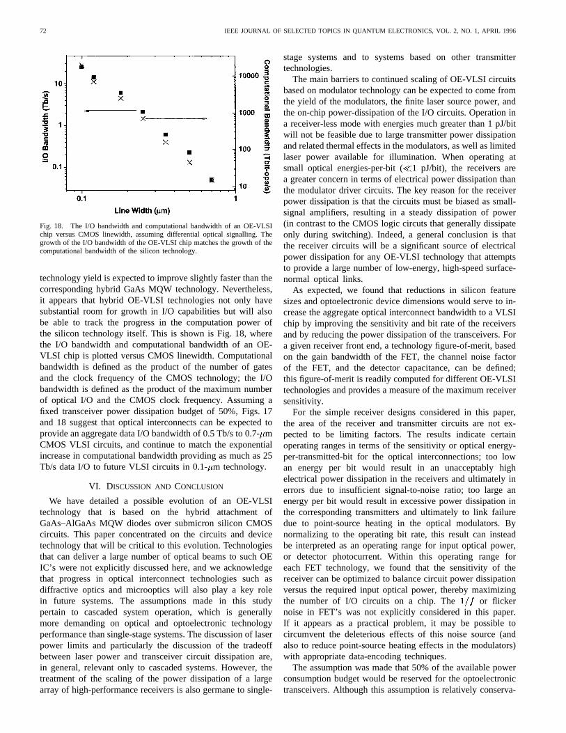
Fig. 18. The I/O bandwidth and computational bandwidth of an OE-VLSIchip versus CMOS linewidth, assuming differential optical signalling. Thegrowth of the I/O bandwidth of the OE-VLSI chip matches the growth of thecomputational bandwidth of the silicon technology.
technology yield is expected to improve slightly faster than thecorresponding hybrid GaAs MQW technology. Nevertheless,it appears that hybrid OE-VLSI technologies not only havesubstantial room for growth in I/O capabilities but will alsobe able to track the progress in the computation power ofthe silicon technology itself. This is shown is Fig. 18, wherethe I/O bandwidth and computational bandwidth of an OE-VLSI chip is plotted versus CMOS linewidth. Computationalbandwidth is defined as the product of the number of gatesand the clock frequency of the CMOS technology; the I/Obandwidth is defined as the product of the maximum numberof optical I/O and the CMOS clock frequency. Assuming afixed transceiver power dissipation budget of 50%, Figs. 17and 18 suggest that optical interconnects can be expected toprovide an aggregate data I/O bandwidth of 0.5 Tb/s to 0.7-mCMOS VLSI circuits, and continue to match the exponentialincrease in computational bandwidth providing as much as 25Tb/s data I/O to future VLSI circuits in 0.1-m technology.
VI. DISCUSSION AND CONCLUSION
We have detailed a possible evolution of an OE-VLSItechnology that is based on the hybrid attachment ofGaAs–AlGaAs MQW diodes over submicron silicon CMOScircuits. This paper concentrated on the circuits and devicetechnology that will be critical to this evolution. Technologiesthat can deliver a large number of optical beams to such OEIC’s were not explicitly discussed here, and we acknowledgethat progress in optical interconnect technologies such asdiffractive optics and microoptics will also play a key rolein future systems. The assumptions made in this studypertain to cascaded system operation, which is generallymore demanding on optical and optoelectronic technologyperformance than single-stage systems. The discussion of laserpower limits and particularly the discussion of the tradeoffbetween laser power and transceiver circuit dissipation are,in general, relevant only to cascaded systems. However, thetreatment of the scaling of the power dissipation of a largearray of high-performance receivers is also germane to single-
stage systems and to systems based on other transmittertechnologies.
The main barriers to continued scaling of OE-VLSI circuitsbased on modulator technology can be expected to come fromthe yield of the modulators, the finite laser source power, andthe on-chip power-dissipation of the I/O circuits. Operation ina receiver-less mode with energies much greater than 1 pJ/bitwill not be feasible due to large transmitter power dissipationand related thermal effects in the modulators, as well as limitedlaser power available for illumination. When operating atsmall optical energies-per-bit (1 pJ/bit), the receivers area greater concern in terms of electrical power dissipation thanthe modulator driver circuits. The key reason for the receiverpower dissipation is that the circuits must be biased as small-signal amplifiers, resulting in a steady dissipation of power(in contrast to the CMOS logic circuts that generally dissipateonly during switching). Indeed, a general conclusion is thatthe receiver circuits will be a significant source of electricalpower dissipation for any OE-VLSI technology that attemptsto provide a large number of low-energy, high-speed surface-normal optical links.
As expected, we found that reductions in silicon featuresizes and optoelectronic device dimensions would serve to in-crease the aggregate optical interconnect bandwidth to a VLSIchip by improving the sensitivity and bit rate of the receiversand by reducing the power dissipation of the transceivers. Fora given receiver front end, a technology figure-of-merit, basedon the gain bandwidth of the FET, the channel noise factorof the FET, and the detector capacitance, can be defined;this figure-of-merit is readily computed for different OE-VLSItechnologies and provides a measure of the maximum receiversensitivity.
For the simple receiver designs considered in this paper,the area of the receiver and transmitter circuits are not ex-pected to be limiting factors. The results indicate certainoperating ranges in terms of the sensitivity or optical energy-per-transmitted-bit for the optical interconnections; too lowan energy per bit would result in an unacceptably highelectrical power dissipation in the receivers and ultimately inerrors due to insufficient signal-to-noise ratio; too large anenergy per bit would result in excessive power dissipation inthe corresponding transmitters and ultimately to link failuredue to point-source heating in the optical modulators. Bynormalizing to the operating bit rate, this result can insteadbe interpreted as an operating range for input optical power,or detector photocurrent. Within this operating range foreach FET technology, we found that the sensitivity of thereceiver can be optimized to balance circuit power dissipationversus the required input optical power, thereby maximizingthe number of I/O circuits on a chip. The or flickernoise in FET’s was not explicitly considered in this paper.If it appears as a practical problem, it may be possible tocircumvent the deleterious effects of this noise source (andalso to reduce point-source heating effects in the modulators)with appropriate data-encoding techniques.
The assumption was made that 50% of the available powerconsumption budget would be reserved for the optoelectronictransceivers. Although this assumption is relatively conserva-
KRISHNAMOORTHY AND MILLER: SCALING OPTOELECTRONIC-VLSI CIRCUITS INTO THE 21ST CENTURY 73
tive when compared to custom submicron electronic chips,individual OE-VLSI circuit applications would be expectedto have differing requirements; this would directly affectthe optimum receiver sensitivity. Assuming that the receiversensitivity is optimized, the limit to the number of optical I/O isprimarily due to the number of optical diodes available, thoughreceiver power dissipation is close to the allowable limits also.Nevertheless, it appears that the growth of the I/O bandwidthof the OE-VLSI chip can be expected to match the growth ofthe computational bandwidth of the silicon technology. Indeed,an aggregate I/O bandwidth (assuming two-beam operation)on the order of 0.5 Tb/s with 0.7-m CMOS and up to 25Tb/s with future 0.1- m CMOS technologies appears to bepossible, despite some relatively conservative assumptions onoptoelectronic device performance.
The receiver design considered in this paper was based onan asynchronous transimpedance feedback amplifier that hasproven characteristics of high bandwidth, dynamic range, andtolerance to device mismatch. This choice of receiver frontend allowed a reasonably accurate estimate to be made forthe RMS noise currents, and hence the receiver sensitivity.However, like all circuits that require biasing to achieve highsensitivity, the transimpedance amplifier draws static currentwhich leads to static power dissipation. It is possible to trade inthe static power dissipation of the receiver for bandwidth, sen-sitivity, or system complexity. Designs for alternate receivercircuits are explored in greater depth elsewhere [112]. Onemethod to reduce this static power dissipation is to use timinginformation that may be available in the system. This wouldallow the power supplies to be clocked so as to reduce theactive biasing period. This is the rationale behind the use ofsynchronous sense-amplifier receivers circuits as discussed in[113]. Naturally, this improvement in power dissipation wouldcome at the price of more exacting system timing constraintsand possibly reduced receiver bandwidth. While this tradeoffmay be particularly advantageous for synchronous systemoperation, it may be unsuitable in instances where precisetiming information is unavailable. To preserve the generality ofthe paper, we chose to model an asynchronous circuit such asthe transimpedance receiver. The details of the derivation andresults presented in this paper would allow the reader to readilyinterpret the effects of a constant factor in power dissipationafforded by specific optimizations of the transceiver circuits.
In terms of the fundamental technology, the challengesare in reducing the drive voltages of the modulators to staycompatible with mainstream CMOS, to provide sufficient laserpower, and to continue to improve the yield in the manu-facturing and hybridizing of the MQW diodes. An importantgeneral conclusion that does not depend critically on thedetailed assumptions is that it appears this hybrid optical I/Otechnology has substantial room for continued scaling to largernumbers of higher speed interconnects as silicon technologyitself advances.
ACKNOWLEDGMENT
The authors express their gratitude to T. Woodward, A.Lentine, and B. Mansoorian for many illuminating discussionson receivers; to K. Devenport for his assistance in the analysis
and simulations of transimpedance receiver stability; to K.Goossen for profitable discussions on the operating voltageand yield of the hybrid MQW modulators, and especially toR. Novotny for valuable input on point source heating effectsand the scaling of the MQW diode capacitance and thermalresistance. The authors also thank two anonymous reviewersfor their comments on the manuscript.
REFERENCES
[1] Semiconductor Industry Association,The National Technology Roadmapfor Semiconductors, 1993–1994, p. B2.
[2] K. M. Johnson, M. A. Handschy, and L. A. Pagano-Stauffer, “Opticalcomputing and image processing with ferroelectric liquid crystal,”Opt.Eng., vol. 26, no. 5, pp. 385–391, 1987.
[3] T. J. Drabik and M. A. Handschy, “Silicon VLSI/ferroelectric liquidcrystal technology fro micropower optoelectronic computing devices,”Appl. Opt., vol. 29, no. 35, pp. 5220–5223, Dec. 1990.
[4] M. J. Goodwin, C. J. K. Kirkby, A. D. Parsons, I. Bennion, and W. J.Stewart, “8�8 element PLZT/silicon spatial light modulator,”Electron.Lett., vol. 25, p. 1260, 1989.
[5] B. Mansoorian, V. Ozguz, C. Fan, and S. Esener, “Design and imple-mentation of flip-chip bonded Si/PLZT smart pixels,” inProc. IEEELEOS Summer Top. Meet. on Smart Pixels, Santa Barbara, CA, Aug.1992, Paper MC2.
[6] N. M. Jokerst, C. Camperi-Ginestet, B. Buchanan, S. Wilkenson, andM. A. Brooke, “Communication through stacked silicon circuitry usingintegrated thin film InP-based emitters and detectors,”IEEE Photon.Technol. Lett., vol. 7, pp. 1028–1030, Sept. 1995.
[7] J. L. Jewell, K. F. Huang, K. Tai, Y. H. Lee, R. J. Fischer, S. L. McCall,and A. Y. Cho, “Vertical cavity single quantum well laser,”Appl. Phys.Lett., vol. 55, pp. 424–426, 1989.
[8] R. Geels, S. Corzine, and L. Coldren, “InGaAs vertical-cavity surfaceemitting lasers,”IEEE J. Quantum Electron., vol. 27, pp. 1359–1367,June 1991.
[9] C. Edge, R. M. Ash, G. G. Jones, and M. J. Goodwin, “Flip-chip solderbond mounting of laser diodes,”Electron. Lett., vol. 27, pp. 499–500,1991.
[10] S. Daryanani, H. Fathollahnejad, D. L. Mathine, R. Droopad, A. Kubes,and G. N. Maracas, “Integration of a single vertical-cavity surfaceemitting laser onto a CMOS inverter chip,”Electron. Lett., vol. 31,no. 10, pp. 833–834, 1995.
[11] D. A. B. Miller, D. S. Chemla, T. C. Damen, A. C. Gossard, W.Wiegmann, T. H. Wood, and C. A. Burrus, “Novel hybrid opticallybistable switch: The quantum well self-electro-optic effect device,”Appl.Phys. Lett., vol. 45, no. 1, pp. 13–15, 1984.
[12] M. J. Goodwin, A. J. Moseley, M. Q. Kearley, R. C. Morris, C. J.G. Kirkby, J. Thomson, R. C. Goodfellow, and I. Bennion, “Opto-electronic component arrays for optical interconnection of circuits andsubsystems,”J. Lightwave Technol., vol. 9, pp. 1639–1645, Dec. 1991.
[13] K. W. Goossen, J. E. Cunningham, and W. Y. Jan, “GaAs 850 nmmodulators solder-bonded to silicon,”IEEE Photon. Technol. Lett., vol.5, pp. 776–778, 1993.
[14] C. Kyriakakis, Z. Karim, A. R. Tanguay, Jr., R. F. Cartland, A.Madhukar, S. Piazolla, B. K. Jenkins, C. B. Kuznia, A. A. Sawchuk, andC. Von der Malsburg, “Photonic implementations of neural networks,”Tech. Dig. OSA Top. Meet. Optical Computing, Salt Lake City, UT, Mar.1995, pp. 128–130.
[15] M. Hansen, D. Shih, C. Fan, and S. Esener, “16�16 SLM with siliconCMOS drivers and III-V modulators,” inProc. OSA Top. Meet. SpatialLight Modulators and Applications, Salt Lake City, UT, Mar. 1995, pp.5–8.
[16] T. L. Worchesky, K. J. Ritter, R. Martin, and B. Lane, “Large arrays ofspatial light modulators hybridized to silicon integrated circuits,”Appl.Opt., vol. 35, no. 8, pp. 1180–1186, Mar. 1996.
[17] K. W. Goossen, J. A. Walker, L. A. D’Asaro, S. P. Hui, B. Tseng,R. Leibenguth, D. Kossives, D. D. Bacon, D. Dahringer, L. M. F.Chirovsky, A. L. Lentine, and D. A. B. Miller, “GaAs MQW modulatorsintegrated with silicon CMOS,”IEEE Photon. Technol. Lett., vol. 7, no.4, pp. 360–362, Apr. 1995.
[18] A. L. Lentine and D. A. B. Miller, “Evolution of the SEED technology:Bistable logic gates to optoelectronic smart pixels,”IEEE J. QuantumElectronics, vol. 29, pp. 655–669, Feb. 1993.
[19] A. V. Krishnamoorthy, A. L. Lentine, K. W. Goossen, J. A. Walker, T.K. Woodward, J. E. Ford, G. F. Aplin, L. A. D’Asaro, S. P. Hui, B.Tseng, R. Leibenguth, D. Kossives, D. Dahringer, L. M. F. Chirovsky,
74 IEEE JOURNAL OF SELECTED TOPICS IN QUANTUM ELECTRONICS, VOL. 2, NO. 1, APRIL 1996
and D. A. B. Miller, “3-D integration of MQW modulators overactive sub-micron CMOS circuits: 375 Mb/s transimpedance receiver-transmitter circuit,”IEEE Photon. Technol. Lett., vol. 7, pp. 1288–1290,Nov. 1995.
[20] A. V. Krishnamoorthy, J. E. Ford, K. W. Goossen, J. A. Walker, A. L.Lentine, L. A. D’Asaro, S. P. Hui, B. Tseng, R. Leibenguth, D. Kossives,D. Dahringer, L. M. F. Chirovsky, F. E. Kiamilev, G. F. Aplin, R. G.Rozier, and D. A. B. Miller, “Photonic page buffer based on GaAsMQW modulators bonded directly over active silicon CMOS circuits,”Appl. Opt., vol. 35, no. 14, pp. 2439–2448, May 1996.
[21] A. L. Lentine, K. W. Goossen, J. A. Walker, L. M. F. Chirovsky, L. A.D’Asaro, S. P. Hui, B. Tseng, R. Leibenguth, J. E. Cunningham, W. Y.Jan, J. M. Kuo, D. Dahringer, D. Kossives, D. Bacon, G. Livescue, R. L.Morrison, R. A. Novotny, and D. B. Buchholz, “Optoelectronic VLSIswitching chip with greater than 4000 optical I/O based on flip-chipbonding of GaAs/AlGaAs MQW modulators and detectors to siliconCMOS,” Conf. Lasers and Electro-Opt. (CLEO-’96), May 1996, vol. 9,pp. 517–518; see also this issue, pp. 77–84.
[22] T. K. Woodward, A. V. Krishnamoorthy, A. L. Lentine, K. W. Goossen,J. A. Walker, J. E. Cunningham, W. Y. Jan, L. A. D’Asaro, L. M.F. Chirovsky, S. P. Hui, B. Tseng, D. Kossives, D. Dahringer, andR. Leibenguth, “1 Gb/s two-beam transimpedance smart-pixel opticalreceivers made from hybrid GaAs MQW modulators bonded to 0.8�msilicon CMOS,” IEEE Photon. Technol. Lett., vol. 8, pp. 422–444, Mar.1996.
[23] D. A. B. Miller and H. Ozaktas, “Limit to the bit-rate capacity ofelectrical interconnects from the aspect ratio of the system architec-ture,” J. Parallel and Distributed Computing, Special Issue on OpticalInterconnects, to be published.
[24] E. J. Novak, “Ultimate CMOS ULSI performance,”IEDM Tech. Dig.,pp. 115–118, 1993.
[25] B. Davari, R. H. Dennard, and G. G. Shahidi, “CMOS scaling for highperformance and low power—The next ten years,”Proc. IEEE, vol. 83,pp. 595–606, Apr. 1995.
[26] J. D. Meindl, “Low power microelectronics, retrospect and prospect,”Proc. IEEE, vol. 83, pp. 619–635, Apr. 1995.
[27] M. Bohr, “MOS transistors: Scaling and performance trends,”Semicond.Int., pp. 75–78, June 1995.
[28] Y. Taur, Y.-J. Mii, D. J. Frank, H.-S. Wong, D. A. Buchanan, S. J. Wind,S. A. Rishton, G. A. Sai-Halasz, and E. J. Nowak, “CMOS scaling intothe 21st century: 0.1�m and beyond,”IBM J. Res. Develop., vol. 39,no. 1/2, Jan./Mar. 1995.
[29] G. Groeseneken, R. Bellens, G. Van den Bosch, and H. E. Maes, “Hotcarrier degradation in submicrometer MOSFETs: From uniform injectiontoward the real operating conditions,”Semicond. Sci. Technol., vol. 10,pp. 1208–1220, 1995.
[30] C. A. Warwick, R. H. Yan, Y. O. Kim, and A. Ourmazd, “Towardgiga-scale silicon integrated circuits,”AT&T Tech. J., pp. 50–59, Sept.1993.
[31] R. H. Yan, D. Monroe, J. Weis, A. Mujtaba, and E. Westerwick,“Reducing operating voltage from 3, 2, to 1 volt and below: Challengesand guidelines for possible solutions,”IEDM Tech. Dig., pp. 55–58,1995.
[32] N. H. E. Weste and K. Eshraghian,Principles of CMOS VLSI Design:A Systems Perspective. Reading, MA: Addison-Wesley, 1993.
[33] A. Hori, H. Nakaoka, H. Umimoto, K. Yamashita, M. Takase, N.Shimizu, B. Mizuno, and S. Odanaka, “A 0.05�m CMOS with ultra-shallow source/drain junctions fabricated by 5 KeV ion implantation andrapid thermal annealing,”IEDM Tech. Dig., pp. 485–488, 1994.
[34] M. Ono, M. Saito, T. Yoshitomi, C. Fiegna, T. Ohguro, and H. Iwai,“Sub-50 nm gate-lengthN -MOSFET’s with 10 nm phosphorus sourceand drain junctions,”IEDM Tech. Dig., pp. 119–122, 1993.
[35] Y. Taur, S. Wind, Y. J. Mii, Y. Lii, D. Moy, K. A. Jenkins, C. L.Chen, P. J. Coane, D. Klaus, J. Bucchignano, M. Rosenfeld, M. G. R.Thomson, and M. Polcari, “High-performance 0.1�m devices with 1.5V power supply,”IEDM Tech. Dig., pp. 127–130, 1993.
[36] G. E. Rittenhouse, W. M. Mansfield, A. Kornblit, R. A. Cirelli, D.Tomes, and G. K. Celler, “Sub-0.1�m NMOS transistors fabricatedusing laser plasma point-source X-Ray lithography,”IEEE ElectronDevice Lett., vol. 16, pp. 322–324, July 1995.
[37] J. Lyu, B.-G. Park, K. Chun, and J. D. Lee, “A novel 0.1�m MOSFETstructure with inverted sidewall and recessed channel,”IEEE ElectronDevice Lett., vol. 17, pp. 157–159, Apr. 1996.
[38] M. Saito, T. Yoshitomi, M. Ono, Y. Akasaka, H. Nii, S. Matsuda,H. S. Momose, Y. Katsumata, Y. Ushiku, and H. Iwai, “An SPDDP -MOSFET structure suitable for 0.1 and sub 0.1 micron channellength and its electrical characteristics,”IEDM Tech. Dig., pp. 897–900,1992.
[39] K. F. Lee, R. H. Yan, D. Y. Jeon, G. M. Chin, Y. O. Kim, D. M.Tennant, B. Razavi, H. D. Lin, Y. G. Wey, E. H. Westerwick, M. D.Morris, R. W. Johnson, T. M. Liu, M. Tarsia, M. Cerullo, R. G. Swartz,and A. Ourmazd, “Room temperature 0.1�m CMOS technology with11.8 ps delay,”IEDM Tech. Dig., pp. 131–134, 1993.
[40] R. H. Yan, K. F. Lee, D. Y. Jeon, Y. O. Kim, B. G. Park, M. R. Pinto,C. S. Rafferty, D. M. Tennant, E. H. Westerwick, G. M. Chin, M. D.Morris, K. Early, P. Mulgrew, W. M. Mansfield, R. K. Watts, A. M.Voshchenkov, J. Bokor, R. G. Swartz, and A. Ourmazd, “89 GHzfTroom-temperature silicon MOSFET’s,”IEEE Electron Device Lett., vol.13, pp. 256–258, May 1992.
[41] K. F. Lee, R. H. Yan, D. Y. Jeon, Y. O. Kim, D. M. Tennant, E. H.Westerwick, K. Early, G. M. Chin, M. D. Morris, R. W. Johnson, T. M.Liu, R. C. Kistler, A. M. Voshchenkov, R. G. Swartz, and A. Ourmazd,“0.1 �m p-channel MOSFET’s with 51 GHzfT ,” IEDM Tech. Dig.,pp. 1012–1014, 1992.
[42] G. G. Shahidi, J. Warnock, S. Fischer, P. A. McFarland, A. Acovic,S. Subbanna, E. Ganin, E. Crabbe, J. Comfort, J. Y.-C. Sun, T. H.Ning, and B. Davari, “High-performance devices for a 0.15�m CMOStechnology,” IEEE Electron Device Lett., vol. 14, pp. 466–468, Oct.1993.
[43] K. Takeuchi, T. Yamamoto, A. Tanabe, T. Matsuki, T. Kunio, M.Fukuma, K. Nakajima, H. Aizaki, H. Miyamoto, and E. Ikawa, “ 0.15�m CMOS with high reliability and performance,”IEDM Tech. Dig.,pp. 883–918, 1993.
[44] S. Subbanna, E. Ganin, E. Crabbe, J. Comfort, S. Wu, P. Agnello,B. Martin, M. McCord, H. Ng, T. Newman, P. McFarland, J. Sun,J. Snare, A. Acovic, A. Ray, R. Gehres, R. Schulz, S. Greco, K.Beyer, L. Liebmann, R. DellaGuardia, and A. Lamberti, “200 nmprocess integration for a 0.15�m channel-length CMOS technologyusing mixed X-ray/optical lithography,”IEDM Tech. Dig., pp. 695–698,1994.
[45] S. Shizumi, T. Kuroi, M. Kobayashi, T. Yamaguchi, T. Fujino, H.Maeda, T. Tsutsumi, Y. Hirose, S. Kusunoki, M. Inuishi, and N.Tsubouchi, “0.15�m CMOS process for high performance and highreliability,” IEDM Tech. Dig., pp. 67–70, 1994.
[46] M. Rodder, S. Aur, and I.-C. Chen, “A scaled 1.8 V, 0.18�m gatelength CMOS technology: Device design and reliability considerations,”IEDM Tech. Dig., pp. 415–418, 1995.
[47] T. Mogami, H. Wakabayashi, Y. Saito, T. Matsuki, T. Tatsumi, andT. Kunio, “A novel salicide process for sub-quarter micron CMOSdevices,”IEDM Tech. Dig., pp. 687–690, 1994.
[48] T. Izawa, M. Katsube, Y. Yokoyama, K. Hashimoto, E. Kawamura, A.Shimizu, H. Takagi, F. Inoue, H. Shimizu, K. Furumochi, H. Goto, S.Kawamura, K. Watanabe, and K. Aoyama, “A novel embedded SRAMtechnology with 10�m2 full CMOS cells for 0.25�m logic devices,”IEDM Tech.Dig., pp. 941–943, 1994.
[49] M. Rodder, A. Amerasekera, S. Aur, and I. C. Chen, “A study ofdesign/process dependence of 0.25�m gate length CMOS for improvedperformance and reliability,”IEDM Tech. Dig., pp. 71–74, 1994.
[50] M. S. C. Luo, P. V. G. Tsui, W.-M. Chen, P. V. Gilbert, B. Maiti, A.R. Sitaram, and S.-W. Sun, “A 0.25�m CMOS technology with 45ANO-nitrided oxide,”IEDM Tech. Dig., pp. 691–694, 1995.
[51] M. Bohr, S. U. Ahmed, L. Brigham, R. Chau, R. Gasser, R. Green,W. Hargrove, E. Lee, R. Natter, S. Thomson, K. Weldon, and S. Yang,“A high-performance 0.35�m logic technology for 3.3 V and 2.5 Voperation,”IEDM Tech. Dig., pp. 273–276, 1994.
[52] R. A. Chapman, C. C. Wei, D. A. Bell, S. Aur, G. A. Brown, and R. A.Haken, “0.5 micron CMOS for high performance,”IEDM Tech. Dig.,pp. 52–55, 1988.
[53] P. G. Y. Tsui, P. V. Gilbert, and S. W. Sun, “Integration of powerLDMOS into a low-voltage 0.5�m BiCMOS technology,”IEDM Tech.Dig., pp. 27–30, 1992.
[54] T. M. Liu, G. M. Chin, D. Y. Jeon, M. D. Morris, V. D. Archer, H.H. Kim, M. Cerullo, K. F. Lee, J. M. Sung, K. Lau, T. Y. Chiu, A.M. Voshchenkov, and R. G. Swartz, “A half-micron super self-alignedBiCMOS technology for high speed applications,”IEDM Tech. Dig.,pp. 23–26, 1992.
[55] Y. Kinoshita, K. Imai, H. Yoshida, H. Suzuki, T. Tatsumi, and T.Yamazaki, “Process integration technology for sub-30 ps ECL BiCMOSusing heavily Boron doped epitaxial contact (HYDEC),”IEDM Tech.Dig., pp. 441–444, 1994.
[56] D. L. Harame, E. F. Crabb´e, J. D. Cressler, J. H. Comfort, J. Y.-C.Sun, S. R. Stiffler, E. Kobeda, J. N. Burghartz, M. M. Gilbert, J. C.Malinowski, A. J. Dally, S. Ratanaphanyarat, M. J. Saccamango, W.Rausch, J. Cotte, C. Chu, and J. M. C. Stork, “A high performanceepitaxial SiGe-base ECL BiCMOS technology,”IEDM Tech. Dig., pp.19–22, 1992.
KRISHNAMOORTHY AND MILLER: SCALING OPTOELECTRONIC-VLSI CIRCUITS INTO THE 21ST CENTURY 75
[57] S. Subbanna, D. Harame, B. Chappell, J. Comfort, B. Davari, R. Franch,D. Danner, A. Acovic, S. Brodsky, J. Gilbreth, D. Robertson, J. Mali-nowski, T. Lii, and G. Shahidi, “A novel borderless contact/interconnecttechnology using aluminum oxide etch stop for high performance logic,”IEDM Tech. Dig., pp. 441–444, 1993.
[58] K. Kasai, Y. Akasaka, K. Nakajima, S. Suehiro, S. Suguro, H. Oyamatsu,M. Kinugawa, and M. Kakumu, “W/WNx/Poly-Si gate technology forfuture high speed deep submircron CMOS LSI’s,”IEDM Tech. Dig.,pp. 497–500, 1994.
[59] J. R. Pfiester, J. D. Shott, and J. D. Meindl, “Performance limits ofCMOS ULSI,” IEEE J. Solid-State Circiuts, vol. SC-20, p. 253, 1985.
[60] P. K. Chatterjee, W. R. Hunter, T. C. Holloway, and Y. T. Lin, “Theimpact of scaling laws on the choice ofn-channel orp-channel for MOSVLSI,” IEEE Electron Device Lett., vol. EDL-1, pp. 220–223, Oct. 1980.
[61] S. Wong and C. A. T. Salama, “Impact of scaling on MOS analogperformance,”IEEE J. Solid-State Circuits, vol. SC-18, pp. 106–114,Feb. 1983.
[62] D. Scifres,Spectra Diode Labs., private communication.[63] R. A. Novotny, A. L. Lentine, D. B. Buchholz, and A. V. Krishnamoor-
thy, “Analysis of parasitic front-end capacitance and thermal resistancein hybrid flip-chip bonded GaAs SEED/Si CMOS receivers,” inTech.Dig. OSA Top. Meet. on Optical Computing, Salt Lake City, UT, Mar.1995, pp. 207–209.
[64] A. V. Krishnamoorthy, T. K. Woodward, R. A. Novotny, K. W.Goossen, J. A. Walker, A. L. Lentine, L. A. D’Asaro, S. P. Hui, B.Tseng, R. Leibenguth, D. Kossives, D. Dahringer, L. M. F. Chirovsky,G. F. Aplin, R. G. Rozier, F. E. Kiamilev, and D. A. B. Miller, “Ringoscillators with optical and electrical readout based on hybrid GaAsMQW modulators bonded to 0.8 micron CMOS,”Electron. Lett., vol.31, no. 22, pp. 1917–1918, Oct. 1995.
[65] R. A. Novotny, “Analysis of smart-pixel digital logic and opticalinterconnection,” Ph.D. Dissertation, Heriot Watt University, U.K.,1996.
[66] T. Sakurai and K. Tamaru, “Simple formulas for two- and three-dimensional capacitances,”IEEE Trans. Electron Devices, vol. ED-30,pp. 183–185, Feb. 1983.
[67] L. M. F. Chirovsky, M. W. Focht, J. M. Freund, G. D. Guth, R. E.Leibenguth, G. J. Przybylek, L. E. Smith, L. A. D. Asaro, A. L. Lentine,R. A. Novotny, and D. B. Huchholz, “Large arrays of symmetric self-electro-optic-effect devices,” inTech. Dig. OSA Top. Meet. on OpticalComputing, Salt Lake City, UT, Mar. 1991, pp. 150–153.
[68] H. S. Hinton, T. J. Cloonan, F. B. McCormick, A. L. Lentin, and F. A.P. Tooley, “Free-space digital optical systems,”Proc. IEEE, Nov. 1994,vol. 82, pp. 1632–1649.
[69] T. Sizer, II, R. E. La Marche, and T. K. Woodward, “Point-sourceheating effects in multiple quantum well modulators,”Appl. Phys. Lett.,vol. 61, no. 4, pp. 420–422, July 1992.
[70] A. L. Lentine, K. W. Goossen, J. A. Walker, L. M. F. Chirovsky, L. A.D’Asaro, S. P. Hui, B. T. Tseng, R. E. Leibenguth, D. P. Kossives. D. W.Dahringer, D. D. Bacon, T. K. Woodward, and D. A. B. Miller, “Arraysof optoelectronic switching nodes comprised of flip-chip bonded MQWmodulators and detectors on silicon CMOS circuitry,”IEEE Photon.Technol. Lett., vol. 8, pp. 221–223, Feb. 1996.
[71] K. W. Goossen, J. E. Cunningham, and W. Y. Jan, “Stacked-diodeelectroabsorption modulator,”IEEE Photon. Technol. Lett., vol. 6, pp.936–938, Aug. 1994.
[72] M. Whitehead, A. W. Rivers, G. Parry, and J. S. Roberts, “Very lowvoltage, normally-off asymmetric Fabry-Perot reflection modulator,”Electron. Lett., vol. 26, pp. 1588–1590, 1990.
[73] R. H. Yan, R. J. Simes, and L. A. Coldren, “Surface normal electroab-sorption reflection modulators using asymmetric Fabry-Perot structures,”IEEE J. Quantum Electron., vol. 27, pp. 1922–1931, 1991.
[74] B. Pezeshki, D. Thomas, and J. S. Harris, “Optimization of modulationratio and insertion loss in reflective electroabsorptive modulators,”Appl.Phys. Lett., vol. 57, pp. 1491–1492, 1990.
[75] P. Zouganeli, M. Whitehead, P. J. Stevens, A. W. Rivers, G. Parry,and J. S. Roberts, “High tolerances for a low voltage, high contrast,low insertion loss asymmetric Fabry-Perot modulator,”IEEE Photon.Technol. Lett., vol. 3, pp. 733–735, Aug. 1991.
[76] P. Zouganeli and G. Parry, “Design tradeoffs and evalation of the perfor-mance attainable by GaAs–Al0:3Ga0:7As asymmetric Fabry-Perot mod-ulators,” IEEE J. Quantum Electron., vol. 31, pp. 927–943, May 1995.
[77] K. W. Goossen, J. E. Cunningham, W. Y. Jan, and J. Centanni, “High-yield, low cost Fabry–Perot modulators utilizing correctable partialanti-reflection coatings,”Appl. Phys. Lett., vol. 66, no. 9, pp. 1041–1043,Feb. 1995.
[78] F. B. McCormick, T. J. Cloonan, A. L. Lentine, J. M. Saisan, R. L.Morrison, M. G. Beckman, S. L. Walker, M. J. Wojcik, S. J. Hinterlong,
R. J. Crisci, R. A. Novotny, and H. S. Hinton, “Five-stage free-spaceoptical switching network with field-effect transistor self-electro-optic-effect-device smart-pixel arrays,”Appl. Opt., vol. 33, pp. 1601–1618,1994.
[79] A. V. Krishnamoorthy, T. K. Woodward, K. W. Goossen, J. A. Walker,B. Tseng, S. P. Hui, J. E. Cunningham, W. Y. Jan, F. E. Kiamilev,and D. A. B. Miller, “Operation of a dual-function receiver/transmitterhybrid CMOS SEED circuit,”Appl. Opt., to be published in Sept. 1996.
[80] A. V. Krishnamoorthy, T. K. Woodward, K. W. Goossen, J. A. Walker,A. L. Lentine, L. M. F. Chirovsky, S. P. Hui, B. Tseng, R. Leibenguth,J. E. Cunningham, and W. Y. Jan, “Operation of a single-ended 550Mbit/s, 41 fJ, Hybrid CMOS/MQW receiver,”Electron. Lett., vol. 32,no. 8, pp. 764–765, Apr. 1996.
[81] D. Liu and C. Svensson, “Power consumption estimation in CMOSVLSI chips,” IEEE J. Solid-State Circiuts, vol. 29, pp. 663–670, June1994.
[82] A. A. Abidi, “Gigahertz transresistance amplifiers in fine lineNMOS,”IEEE J. Solid-State Circiuts, vol. SC-19, pp. 986–994, Dec. 1984.
[83] R. A. Novotny, M. J. Wojcik, A. L. Lentine, L. M. F. Chirovsky, L. A.D’Asaro, M. W. Focht, G. Guth, K. G. Glogovsky, R. Leibenguth, M. T.Asom, and J. M. Freund, “FET-SEED differential transimpedance am-plifiers for two-dimensional optical data links,”J. Lightwave Technol.,vol. 13, pp. 606–614, Apr. 1995.
[84] M. Ingels, G. Van der Plas, J. Crols, and M. Steyaert, “A CMOS 18THz 240 Mb/s transimpedance amplifier and 155 Mb/s LED-driverfor low cost optical fiber links,”IEEE J. Solid-State Circiuts, vol. 29,pp. 1552–1559, Dec. 1994.
[85] A. A. Ketterson, J.-W. Seo, M. H. Tong, K. L. Nummila, J. J. Morikuni,K.-Y. Cheng, S.-M. Kang, and I. Adesida, “A MODFET-based opto-electronic integrated circuit receiver for optical interconnects,”IEEETrans. Electron Devices, vol. 40, pp. 1406–1416, Aug. 1993.
[86] M. Govindarajan and S. R. Forrest, “Design considerations for wide-bandp-i-n/HBT monolithic transimpedance optical receivers,”J. Light-wave Technol., vol. 11, pp. 367–378, Feb. 1993.
[87] T. Vanisri and C. Toumazou, “Integrated high frequence low-noisecurrent-mode optical transimpedance preamplifiers: Theory and prac-tice,” IEEE J. Solid-State Circiuts, vol. 30, pp. 677–785, June 1995.
[88] N. Scheinberg, R. J. Bayruns, and T. M. Laverick, “Monolithic GaAstransimpedance amplifiers for fiber-optic receivers,”IEEE J. Solid-StateCirciuts, vol. 26, pp. 1834–1839, Dec. 1991.
[89] B. I. Kasper, “Receiver design,” inOptical Fiber Telecommunications, S.E. Miller and I. P. Kaminow Eds. New York: Springer Verlag, 1982,pp. 689–722.
[90] G. F. Williams and H. P. LeBlanc, “Active feedback lightwave re-ceivers,”J. Lightwave Technol., vol. LT-4, pp. 1502–1508, Oct. 1986.
[91] G. F. Williams, “Lightwave receivers,” inTopics in Lightwave Trans-mission Systems, T. Li, Ed. San Diego, CA: Academic, 1991.
[92] P. E. Allen and D. R. Holberg,CMOS Analog Circuit Design. NewYork: Oxford Univ. Press, 1987.
[93] R. G. Smith and S. D. Personick, “Receiver design for optical fibercommunication systems,” inTopics in Appl. Phys., H. Kressel, Ed.New York: Springer-Verlag, 1982, vol. 39.
[94] Z. H. Fang, S. Cristoloveanu, and A. Chovet, “Analysis of hot-carrier-induced aging from1=f noise in short-channel MOSFET’s,”IEEEElectron Device Lett., vol. EDL-7, pp. 371–373, June 1986.
[95] M. Aoki and M. Kato, “Hole-induced1=f noise increase in MOStransistors,”IEEE Electron Device Lett., vol. 17, pp. 118–120, 1996.
[96] J. J. Morikuni, A. Dharchoudhury, Y. Leblebici, and S. M. Kang,“Improvements to the standard theory for photoreceiver noise,”J.Lightwave Technol., vol. 12, pp. 1174–1183, July 1994.
[97] L. D. Tzeng, R. E. Frahm, and W. Asous, “A high-performance opticalreceiver for 622 Mb/s direct-detection systems,”IEEE Photon. Technol.Lett., vol. 2, pp. 759–761, Oct. 1990.
[98] A. A. Abidi, “On the choice of optimum FET size in wide-bandtransimpedance amplifiers,”J. Lightwave Technol., vol. 6, pp. 64–66,Jan. 1988.
[99] R. P. Jindal, “High-frequency noise in fine-lineNMOS field effecttransistors,”IEDM Tech. Dig., pp. 68–71, 1985.
[100] A. A. Abidi, “High-frequence noise measurements on FET’s with smalldimensions,”IEEE Trans. Electron Devices, vol. ED-33, pp. 1801–1805,Nov. 1986.
[101] K. Ogawa, B. Owen, and H. J. Boll, “A long wavelength optical receiverusing a short channel Si-MOSFET,”Bell System Tech. J., vol. 62, no.5, pp. 1181–1188, May-June 1983.
[102] S. M. Sze,High-Speed Semiconductor Devices. New York: Wiley,1990.
[103] R. L. Geiger, P. E. Allen, and N. R. Strader,VLSI Design Techniquesfor Analog and Digital Circuits. New York: McGraw Hill, 1990, ch. 3.
76 IEEE JOURNAL OF SELECTED TOPICS IN QUANTUM ELECTRONICS, VOL. 2, NO. 1, APRIL 1996
[104] T. K. Woodward, A. L. Lentine, L. M. F. Chirovsky, M. W. Focht,J. M. Freund, G. D. Guth, R. E. Leibenguth, L. E. Smith, L. A.D’Asaro, E. J. Laskowski, and S. S. Pei, “GaAs/AlGaAs FET-SEEDreceivers/transmitters,” inOSA Proc. Photon. Switching, J. W. Goodmanand R. C. Alferness, Eds. Washington, DC: Opt Soc. Amer., 1993,vol. 16, pp. 89–93.
[105] W. Fischer, “Equivalent circuit and gain of MOS field effect transistors,”Solid State Electron., vol. 9, pp. 71–81, 1966.
[106] T. Nakahara, S. Matsuo, S. Fukushima, and T. Kurokawa, “Perfor-mance comparison between multiple quantum-well modulator-based andvertical-cavity-surface-emitting-laser-based smart pixels,”Appl. Opt.,vol. 35, no. 5, pp. 860–871, Feb. 1996.
[107] C. Fan, B. Mansoorian, D. A. Van Blerkom, M. Hansen, V. H.Ozguz, S. C. Esener, and G. C. Marsden, “Digital free-space opticalinterconnections: A comparison of transmitter technologies,”Appl. Opt.,vol. 34, no. 17, pp. 3103–3115, June 1995.
[108] A. V. Krishnamoorthy, P. J. Marchand, F. E. Kiamilev, and S. C. Esener,“Grain-size considerations for optoelectronic multistage-interconnectionnetworks,”Appl. Opt., vol. 31, no. 26, pp. 5480–5507, Sept. 1992.
[109] H. M. Ozaktas and J. W. Goodman, “Elements of a hybrid interconnec-tion theory,” Appl. Opt., vol. 33, no. 14, pp. 2968–2987, 1994.
[110] T. J. Drabik, “Optoelectronic integrated systems based on free-spaceinterconnects with an arbitrary degree of space variance,”Proc. IEEE,vol. 82, pp. 1595–622, Nov. 1994.
[111] C. W. Stirk, “Cost-performance tradeoffs in optical interconnects,” inTech. Dig. OSA Top. Meet. on Optical Computing, Salt Lake City, UT,Mar. 1995, pp. 105–107.
[112] T. K. Woodward, A. V. Krishnamoorthy, A. L. Lentine, and L. M. F.Chirovsky, “Optical receivers for optoelectronic VLSI,” this issue, pp.106–116.
[113] T. K. Woodward, A. V. Krishnamoorthy, K. W. Goossen, J. A. Walker,J. E. Cunningham, W. Y. Jan, L. M. F. Chirovsky, S. P. Hui, B.Tseng, D. Kossives, D. Dahringer, D. Bacon, and R. E. Leibenguth,“Clocked-sense-amplifier-based smart pixel optical recievers,”IEEEPhoton. Technol. Lett., vol. 8, Aug. 1996.
Ashok V. Krishnamoorthy (S’90–M’93) receivedthe B.S. degree with honors from the CaliforniaInstitute of Technology, Pasadena, in 1986, theM.S.E.E. degree from the University of SouthernCalifornia, Los Angeles, in 1988, and the Ph.D.degree in electrical engineering from the Universityof California, San Diego (UCSD), in 1993.
After spending a year as a Research Scientist inthe Electrical & Computer Engineering Departmentat UCSD, he joined the Advanced Photonics Re-search Deparment at Bell Laboratories as a Member
of Technical Staff in 1994. His research interests are in the area of opticalinterconnects, optoelectronic-VLSI smart pixels and their application to par-allel computing, memory-access, and switching. He has published over 20journal papers and one book chapter, presented over 10 conference invitedtalks, and filed more than 10 patents. He has served on several conferenceprogram committees for the IEEE Laser and Electro-Optics Society (LEOS),IEEE Computer Society (CS), and the Optical Society of America (OSA),and is the program chair for the 1997 IEEE LEOS Workshop on High-SpeedInterconnections within Digital Systems.
Dr. Krishnamoorthy is a member of Tau Beta Pi, Sigma Xi, OSA, and SPIE.
David A. B. Miller (M’84–SM’89–F’95) received the B.Sc. degree inphysics from St. Andrews University and the Ph.D. degree from Heriot-WattUniversity, U.K., in 1979.
He was a Carnegie Research Scholar at Heriot-Watt, where he continuedto work, after receiving the Ph.D. degree, as a Lecturer in the Departmentof Physics. He moved to AT&T Bell Laboratories in 1981 as a Member ofTechnical Staff, and from 1987 to 1996 was Department Head, latterly of theAdvanced Photonics Research Department. Since August 1996, he has been aProfessor of Electrical Engineering at Stanford University, Stanford, CA. Hisresearch interests include optical switching and processing, nonlinear opticsin semiconductors, and the physics of quantum-confined structures. He haspublished over 170 technical papers and four book chapters, delivered over60 conference invited talks and over 25 short courses, and holds more than30 patents. He has been a member or chair of over 25 technical conferencecommittees, and was General Co-Chair for the Conference on Lasers andElectro-Optics in 1996. He has held posts or served on committees for theIEEE Lasers and Electro-Optics Society (LEOS), for the Optical Society ofAmerica (OSA), for the Optoelectronics Industry Development Association,for the Defense Advanced Research Projects Agency, and on several scientificjournal editorial boards. He was President of the IEEE LEOS in 1995.
Dr. Miller is a fellow of the Royal Society of London, the Optical Society ofAmerica, and the American Physical Society. For his work on semiconductornonlinear optics, quantum well optical properties, and novel devices, he wasawarded the 1986 Adolph Lomb Medal of the OSA, was co-recipient of the1988 R. W. Wood Medal, and received the 1991 Prize of the InternationalCommission for Optics. He was also an IEEE LEOS Traveling Lecturer in1986–87.


![VLSI ARCHITECTURE OF AN AREA EFFICIENT … Edge oriented Image scaling processor [16] ... VLSI Implementation of low-cost high quality image scaling processor [12] is proposed by for](https://img.pdfslide.us/doc/110x75/5b29d2027f8b9a2e1e8b4c98/vlsi-architecture-of-an-area-efficient-edge-oriented-image-scaling-processor-16.jpg)