Embed Size (px)
Citation preview

2009 Workshop on Dependable and Secure Nanocomputing
Scaling Effects on NeutronScaling Effects on Neutron-Induced Soft Error in SRAMs
D 22 PDown to 22nm Process
Production Engineering Research Lab., Hitachi, Ltd.E Ibe Fellow IEEE H Taniguchi Y Yahagi K Shimbo and T TobaE. Ibe, Fellow, IEEE, H. Taniguchi, Y. Yahagi, K. Shimbo, and T. Toba

Contents
1 Fundamentals of Neutron-Induced Soft-Error
Model Description and Validation2
Predicted Scaling Effects3
Discussions 4
Summary5

Contents
1 Fundamentals of Neutron-Induced Soft-Error
Model Description and Validation2
Predicted Scaling Effects3
Discussions 4
Summary5

Macroscopic Mechanism of Terrestrial Neutron Soft-Error1111
Heliomagnetic fieldEnergetic ions from galactic nucleus
Nuclear spallation reaction with Airreaction with Air
Neutron shower
Soft Error
Geomagnetic field
All Rights Reserved Copyright © 2007,Hitachi,Ltd.
Geomagnetic field

Estimated Neutron Spectrum in Tokyo*2222
s) 103
105
1E+01
cm2 /M
eV/
101
10
1E-03
1E-01
Flux
(n/
c
10-3
10-1
1E-05
rent
ial F
10 7
10-5Total Flux:
about 20n/cm2/h
1E-09
1E-07
Diff
er
10 3 100 103 10610-9
10-7(En>1MeV)
1E-03 1E+00 1E+03 1E+0610-3 100 103 106
109 Neutron Energy (eV)
All Rights Reserved Copyright © 2007,Hitachi,Ltd.
*Estimated from the spectrum at the sea level in NewYork(JESD89A,2006)

Microscopic Mechanism of Soft-Error 3333
p+ NodeBallistic neutron Secondary Ionp Node
n+ Noden+ Node
Funneling/Diffusion
y
p-Well
p-Well
++
++
+--
--
-Funneling/DiffusionIsolation
oxide Charge collection to node
n-Well
p Well
Soft-error (flip of stored data)
n Well
Si NucleusResidual
takes place when:Qcol (charge collected )
Nuclear Spallation
ExcitedNucleus
Residual Nucleus(Mg,Al,Na,...)
Evaporated light
>Qcrit (critical charge)
All Rights Reserved Copyright © 2007,Hitachi,Ltd.
NucleonsEvaporated lightnuclei(D,T,α,..)

Current General Trends Retrieved from Literatures4444
10-5SRAM shows increasing trend
10-6
0
DRAMevic
e)
Acceptable
10-7
DRAM
on(cm
2 /de
Acceptable Level
10-9
10-8
oss
Sec
tio
0.1 1 10 100 100010-10
SRAM
SE
U C
r
*SEU Cross Section = Errors/number of incident nucleon
Memory Size (Mb)
0
All Rights Reserved Copyright © 2007,Hitachi,Ltd.
Ibe, E., "Current and Future Trend on Cosmic-Ray-Neutron Induced Single Event Upset at the Ground down to 0.1-Micron-Device," The Svedberg Laboratory Workshop on Applied Physics, Uppsala, May,3, No.1 (2001).

Contents
1 Fundamentals of Neutron-Induced Soft-Error
Model Description and Validation2
Predicted Scaling Effects3
Discussions 4
Summary5
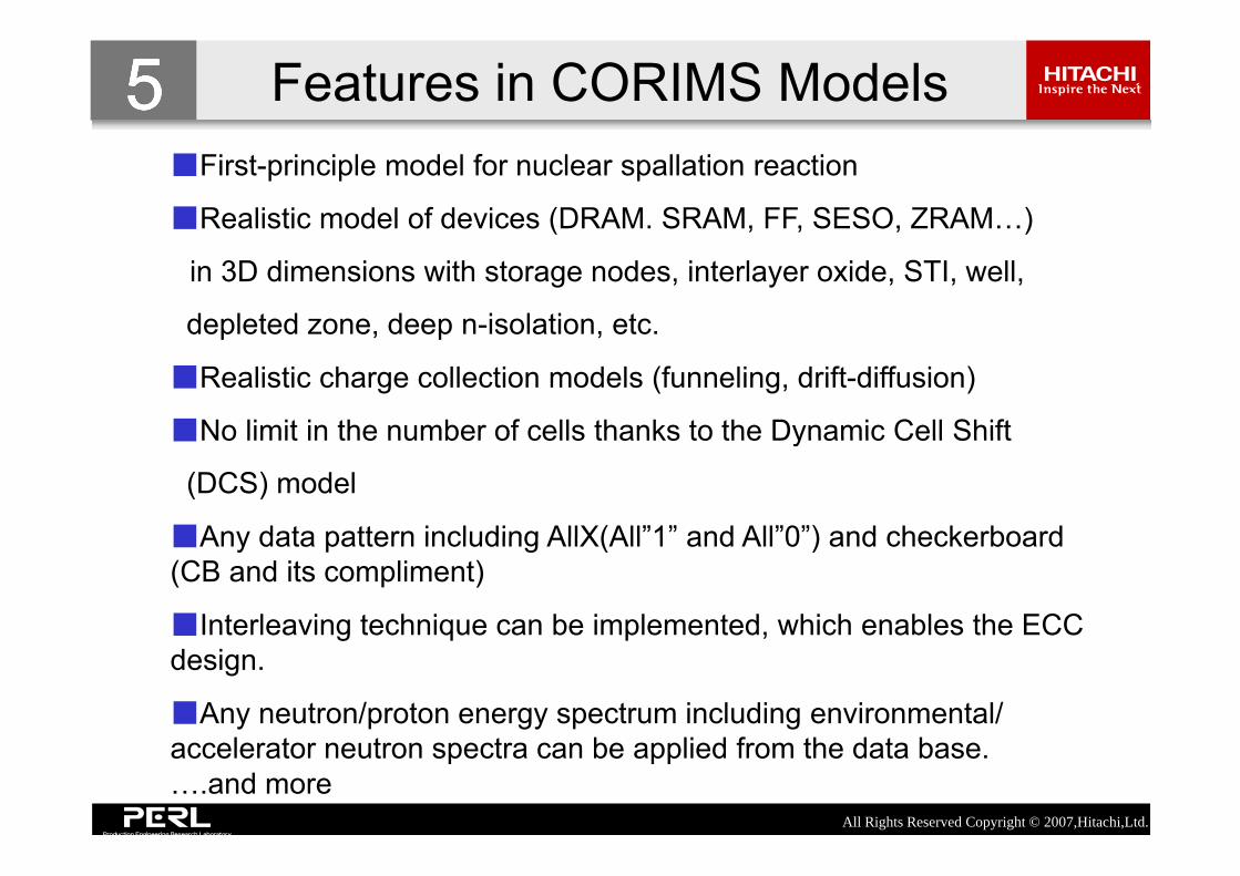
Features in CORIMS Models5555■First-principle model for nuclear spallation reaction
■Realistic model of devices (DRAM. SRAM, FF, SESO, ZRAM…)
in 3D dimensions with storage nodes, interlayer oxide, STI, well,
depleted zone, deep n-isolation, etc.p p
■Realistic charge collection models (funneling, drift-diffusion)
■No limit in the number of cells thanks to the Dynamic Cell Shift■No limit in the number of cells thanks to the Dynamic Cell Shift
(DCS) model
■Any data pattern including AllX(All”1” and All”0”) and checkerboard■Any data pattern including AllX(All 1 and All 0 ) and checkerboard (CB and its compliment)
■Interleaving technique can be implemented, which enables the ECC g q p ,design.
■Any neutron/proton energy spectrum including environmental/
All Rights Reserved Copyright © 2007,Hitachi,Ltd.
accelerator neutron spectra can be applied from the data base. ….and more

SRAM Model6666
bit-line(A) TopView bit-line(A) TopView bit-line(A) TopView
+ p +x
y
z n + n +Channel
A A’
+ p +x
y
z n + n +Channel
A A’
+ p +x
y
z n + n +Channel
A A’
p + p n n
VddBit-
Lin
ep + p n n
VddBit-
Lin
ep + p n n
VddBit-
Lin
e
z
(B) A-A’ Cross Section
GND STI
Word-Linez z
(B) A-A’ Cross Section
GND STI
Word-LineGND STI
Word-Line
p-Well p-Well
n + n +x
y p + p +
p-Well p-Well
n + n +x
y x
y p + p +
n-Well
p Substrate
n-Well
p Substrate
All Rights Reserved Copyright © 2007,Hitachi,Ltd.
p Substratep Substrate

DCS Method 7777■Enables to calculate ion tracks until it stops without any ion range
Actual track
(Xad,Yad+1)(Xad+1,Yad+1)
C Dwithout any ion range limit.
■ Utilizes only one
AddBD”
yphysical cell model (Does not make an NxN cell array)Address
(Xad,Yad)C’C”
NxN cell array)
■Shifts the ion track parallel when it
1 bit reaches the cell boundary and the cell physical address is
A B’p yincremented or decremented according to the boundary
Virtual track
All Rights Reserved Copyright © 2007,Hitachi,Ltd.
to the boundary location.

Data Pattern implementation8888
0110
0101
0110
0101
1001
0110
1001
0110
1001 1001
(a)Unit data pattern(a)Unit data pattern matrix Cell with “1” Cell with “0”
(b) Spreading the matrix onto a device(b) Spreading the matrix onto a device
■Define unit data pattern matrix including CB and AllX
■ Virtually spread the matrix onto a device and the data in a cell can be
All Rights Reserved Copyright © 2007,Hitachi,Ltd.
■ Virtually spread the matrix onto a device and the data in a cell can be calculated according to the physical address.

Display of Part of Cell Array Matrix and Ion tracks9999Data Pattern All”1”
SER Calculation
Spallation area (1 bit)Trace the ion track
til it t t (1 bit)until it stops or gets out of the sensitive
layerError
analysis
Ion TrackIon Track analysis
Nuclear SpallationS ll ti
All Rights Reserved Copyright © 2007,Hitachi,Ltd.
Tracks through nodeTracks through well Node with data “high”(n+)
Spallation

10101010 Validations of the ModelComparison between measured and simulated SERs in
three different locations in Japan
4Mb SRAMAverage
error■Within 20% error for simulations of
i t i4Mb SRAM
1
1.2
.U.] Measured
Si l d
<10% experiments in :
-TSL (Uppsala, Sweden)
CYRIC (Sendai Japan)
0.6
0.8
or R
ate
[A Simulated -CYRIC (Sendai, Japan)
-LANSCE(Los Alamos, USA)
0.2
0.4
Soft
Erro
-RCNP(Osaka,Japan)
010 100 1000 10000
All Rights Reserved Copyright © 2007,Hitachi,Ltd.
Altitude [m]

Assumed Road Map11111111Assumptions
■Cell area decreases by half for each down-scaling.
■ Density doubles. ■Critical charge decreases by half
(In principle, critical charge is in proportion to parasitic capacitance which again in proportion to cell area)proportion to cell area)
■Depth profile does not change
■Operation voltage does not change
Cell area Density QcritSRAM property
Design rule
p g g
nm A.U. Mbit A.U.130 2.1 16 3.290 1 32 1.690 1 32 1.665 0.5 64 0.845 0.25 128 0.432 0 125 256 0 2
All Rights Reserved Copyright © 2007,Hitachi,Ltd.
32 0.125 256 0.222 0.06 512 0.1

Contents
1 Fundamentals of Neutron-Induced Soft-Error
Model Description and Validation2
Predicted Scaling Effects3
Discussions 4
Summary5
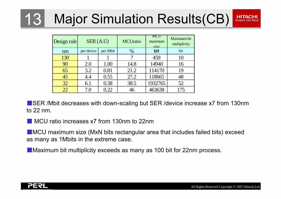
Major Simulation Results(CB)13131313Design rule MCUratio
MCUmaximum
size
Maximum bitmultiplicity
nm per device per Mbit % bit bit
SER (A.U)
130 1 1 7 459 1090 2.0 1.00 14.8 14940 1665 3.2 0.81 21.2 114170 1945 4 4 0 55 27 2 118665 4845 4.4 0.55 27.2 118665 4832 6.1 0.38 38.5 1932765 5222 7.0 0.22 46 463638 175
■SER /Mbit decreases with down-scaling but SER /device increase x7 from 130nm to 22 nm.
■ MCU ratio increases x7 from 130nm to 22nm■ MCU ratio increases x7 from 130nm to 22nm
■MCU maximum size (MxN bits rectangular area that includes failed bits) exceed as many as 1Mbits in the extreme case.
■Maximum bit multiplicity exceeds as many as 100 bit for 22nm process.
All Rights Reserved Copyright © 2007,Hitachi,Ltd.

Spread in Failed Bit Map for All Errors14141414
6080
100120
0
500
500
1000130nm 65nm 45nmroughly100x100
bits
-60-40-20
0204060
-100 -50 0 50
-1000
-500
0-400 -200 0 200 400 600 800
-500
0
500
-600 -400 -200 0 200 400
-300-200-100
0100200300
-200 -100 0 100 200-2000
-1500
-1500
-1000
3000
90nm
-600-500-400300
1000
1500
1000
2000
3000
32nm
22nmWL
BL
-500
0
500
-1000 -500 0 500 1000
-1000
0-1500 -1000 -500 0 500 1000
-2000
-1500
-1000
-3000
-2000 roughly1000x1000
bits
All Rights Reserved Copyright © 2007,Hitachi,Ltd.
bits*Spallation reaction location is the origin.

Shifts in SEU Cross Section15151515
2 0E 072 0E 07
■SEU includes SBU(Single Bit Upset) and MCU(Multi Cell Upset)
1.6E-07
1.8E-07
2.0E-07
m2 /M
eV) 22nm32nm45nm
Total1.6E-07
1.8E-07
2.0E-07
m2 /M
eV) 22nm32nm45nm
TotalCell Upset).
■ The peak in the cross section curves becomes
1.0E-07
1.2E-07
1.4E-07
s Sec
tion
(cm 45nm
65nm90nm130nm1.0E-07
1.2E-07
1.4E-07
s Sec
tion
(cm 45nm
65nm90nm130nm
more apparent and appears at lower energies with down-scaling
4.0E-08
6.0E-08
8.0E-08
fere
tial C
ross
4.0E-08
6.0E-08
8.0E-08
fere
tial C
ross
■The shape of the cross section curves changes from saturation curve
0.0E+00
2.0E-08
0 200 400 600 800
Diff
0.0E+00
2.0E-08
0 200 400 600 800
Diff (130nm) to exponential-like
curves with down scaling
■Contribution of lower0 200 400 600 800
Neutron Energy (MeV)
0 200 400 600 800
Neutron Energy (MeV)■Contribution of lower energy neutron become more significant with down-scaling
All Rights Reserved Copyright © 2007,Hitachi,Ltd.
scaling
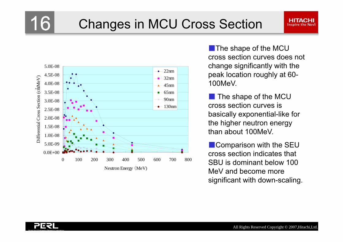
Changes in MCU Cross Section16161616
5 0E 08
■The shape of the MCU cross section curves does not change significantly with the
3.5E-08
4.0E-08
4.5E-08
5.0E-08
(cm2 /M
eV)
22nm32nm45nm65nm
change significantly with the peak location roughly at 60-100MeV.
2.0E-08
2.5E-08
3.0E-08
3.5E 08
Cro
ss S
ectio
n
65nm90nm130nm
■ The shape of the MCU cross section curves is basically exponential-like for th hi h t
5.0E-09
1.0E-08
1.5E-08
Diff
eren
tial the higher neutron energy
than about 100MeV.
■Comparison with the SEU 0.0E+00
0 100 200 300 400 500 600 700 800
Neutron Energy (MeV)
pcross section indicates that SBU is dominant below 100 MeV and become more significant with down-scaling.
All Rights Reserved Copyright © 2007,Hitachi,Ltd.

Shifts in Bit Multiplicity17171717
90100
22
708090
)22nm32nm45nm
405060
Rat
io
(%)
65nm90nm130nm
102030
R 130nm
010
1 10 100
Multiplicity (Bit)
■Bit multiplicity increases with down-scaling
All Rights Reserved Copyright © 2007,Hitachi,Ltd.
■Bit multiplicity increases with down scaling

Contents
1 Fundamentals of Neutron-Induced Soft-Error
Model Description and Validation2
Predicted Scaling Effects3
Discussions 4
Summary5

Factors that Affect Prediction Accuracy18181818
Factor Assumption Possible trend InfluenceFactor Assumption Possible trend Influence
Operation constant decrease Qcrit↓pvoltage
crit↓SER↑
Depth profile constant shallower and SER↓denser
Gate oxide SiO2 HfO Qcrit ↑material (high k) SER↓
Inter-layer SiO2 Low-k Qcrit↓isolation SER↑
All Rights Reserved Copyright © 2007,Hitachi,Ltd.
Implications for Logic Devices19191919■Increases in MCU bit multiplicity and in MCU size imply that MNU(Multi Node Upset:Multiple faults in nodes in a logic device) takes more often
d i idand in wider area.
■ Increase in MNU may impair radiation-hardened device with redundancy nodes like DICEredundancy nodes like DICE.
■ Increase in MNU also implies that logic devices in the vicinity may be failed simultaneouly resulting in impairing redundancy circuits like DMR, y g p g yTMR and so on.
■Nobel radiation hardening techniques have to be developed for logic d i d t ith l b f l i d i ithdevices and systems with a large number of logic devices with reasonable speed/power/area overheads. Interactive countermeasures among device/component/system layers will be effective.
All Rights Reserved Copyright © 2007,Hitachi,Ltd.

Summary21212121■Soft-error rates per device in SRAMs will increase x7
from 130nm to 22nm process.
■ As SRAM is scaled down to smaller size, soft error rate is dominated more significantly by low energy neutrons (<10MeV)
■ The area affected by one nuclear reaction spreads over 1M bits area and bit multiplicity of multi-cell upset become as high as 100 bits and more.
■The discussions are extended to the MNU of logic devices and systems Development of interactivedevices and systems. Development of interactive countermeasures among device/component/system layers is proposed to cope with the real threats in the
All Rights Reserved Copyright © 2007,Hitachi,Ltd.
y p p pfuture.

Reference■ T N k M B b E Ib Y Y h i d H■ T. Nakamura, M. Baba, E. Ibe, Y. Yahagi and H.
Kameyama, Terrestrial Neutron-Induced Soft-Errors in Advanced Memory Devices World Scientific 2008in Advanced Memory Devices, World Scientific, 2008
Thank you for your attention!
All Rights Reserved Copyright © 2007,Hitachi,Ltd.