Embed Size (px)
Citation preview
SC2200 Serial Peripheral Interface Programming Guide UG6336; Rev 0; 9/16 Abstract This document provides the information necessary to develop the hose software to communicate with the SC2200 by way of the Serial Peripheral Interface (SPI).

Page 2/48
CONTENTS
1. Introduction .................................................................................................. 5
1.1. Scope .................................................................................................................................. 5
1.2. Acronyms ............................................................................................................................ 5
1.3. Revision History .................................................................................................................. 5
1.4. References .......................................................................................................................... 6
2. SPI Host Message Interface Protocol ......................................................... 6
2.1. Host Write Operation to Message Interface Buffer ............................................................. 8
2.2. Host Read Operation from Message Interface Buffer ......................................................... 9
2.3. 16-byte Host Message Interface Structure ....................................................................... 10
2.4. Host Message to Read/Write Scratch ............................................................................... 11
2.5. Host Message to Read/Write PRAM ................................................................................. 12
2.6. Host Message for Software Reset .................................................................................... 13
2.7. Host Message to Clear/Set Calibration Parameters ......................................................... 13
3. Global Scratch Parameters ....................................................................... 15
3.1. Device Info Scratch Structure ........................................................................................... 16
3.2. Firmware Status Scratch Structure ................................................................................... 16
3.3. RF Status Scratch Structure ............................................................................................. 17
3.4. Firmware Debugging Information Scratch Structure ......................................................... 17
3.5. PMU Scratch Structure ..................................................................................................... 18
4. Reprogramming the EEPROM with Updated Firmware and Application Parameters ............................. 19
4.1. EEPROM Mapping and Application Parameters .............................................................. 19
4.2. FwConfigPath Structure .................................................................................................... 22
4.3. Device Configuration Structure ......................................................................................... 23
4.4. CAL Parameter Structure .................................................................................................. 23
4.5. Device Advanced Configuration Structure ........................................................................ 24
4.6. Performance Tuning Parameters ...................................................................................... 25
4.7. Meeting Spectral Emission Limits Very Close to Carrier .................................................. 26
4.8. EEPROM Write Instruction ................................................................................................ 27
4.9. EEPROM Read Instruction ............................................................................................... 30
4.10. EEPROM Endurance ........................................................................................................ 30
5. PRAM Application Parameters ................................................................. 31
5.1. To Enable/Disable Correction with PRAM parameter ....................................................... 31
5.2. To Freeze/UnFreeze Adaptation with PRAM parameter ................................................... 32
5.3. To Read back Adaptation State and Correction Enable from PRAM ................................ 33
6. 16-byte Host Message Interface Examples .............................................. 34
6.1. SC2200_Clear_Calibration ............................................................................................... 34
6.2. SC2200_Set_Calibration ................................................................................................... 34
6.3. Reading Device Information from Scratch ........................................................................ 35
6.4. Reading Path A/B FW Status from Scratch ...................................................................... 35
6.5. Reading Device FW Debug Information from Scratch ...................................................... 36
6.6. Clear Info Stack ................................................................................................................. 36
6.7. Read RFIN and RFFB AGC Values .................................................................................. 37
6.8. Read RFIN and RFFB PMU Values .................................................................................. 37
Page 3/48
7. Matlab Example Codes .............................................................................. 38
7.1. SC2200_Read_ApplicationParameters (From EEPROM) ................................................ 38
7.2. SC2200_SetFrequencyScan (In EEPROM) ..................................................................... 41
7.3. SC2200_SetClockRef (In EEPROM) ................................................................................ 43
7.4. SC2200_Get_Device_Information (From Scratch) ........................................................... 43
7.5. SC2200_Get_Device_FW_Status .................................................................................... 44
7.6. SC2200_Get_Paths_Status (From Scratch and PRAM) .................................................. 45
7.7. SC2200_Clear_Calibration ............................................................................................... 47
7.8. SC2200_Set_Calibration ................................................................................................... 48
7.9. Clear InfoStack .................................................................................................................. 48
7.10. Convert16B_Signed SC2200 (PRAM, Scratch and EEPROM) ........................................ 48
List of Tables Table 1: Host Write Operation to Message Interface Buffer ............................................................. 8
Table 2: Host Read Operation from Message Interface Buffer ........................................................ 9
Table 3: Host 16-byte Message Structure ...................................................................................... 10
Table 4: SC2200 16-byte Reply Message Structure ...................................................................... 10
Table 5: Host 16-byte Message to Read/Write Scratch Parameters ............................................. 11
Table 6: Host 16-byte Message to Read/Write Scratch Parameters ............................................. 12
Table 7: Host 16-byte Message for Soft Reset .............................................................................. 13
Table 8: Host 16-byte Message to Clear/Set Calibration Parameters ........................................... 13
Table 9: SC2200 16-byte Reply Message to Clear/Set Calibration Parameters ........................... 13
Table 10: Global Scratch parameters available via SPI Messages ............................................... 15
Table 11: Device Info Structure ...................................................................................................... 16
Table 12: FW Status Structure ....................................................................................................... 16
Table 13: RF Status Structure ........................................................................................................ 17
Table 14: Firmware Debugging Information Structure ................................................................... 17
Table 15: Error Stack Structure ...................................................................................................... 17
Table 16: Info Stack Structure ........................................................................................................ 17
Table 17: Error Code Descriptions ................................................................................................. 17
Table 18: Information Code Descriptions ....................................................................................... 18
Table 19: PMU Structure ................................................................................................................ 18
Table 20: EEPROM Mapping ......................................................................................................... 19
Table 21: EEPROM addresses for Application parameters ........................................................... 20
Table 22: FwConfigPath Structure ................................................................................................. 22
Table 23: Device Configuration Structure ...................................................................................... 23
Table 24: CAL Parameter Structure ............................................................................................... 23
Table 25: Advanced Device Configuration Structure...................................................................... 24
Table 26: Performance Tuning Parameters ................................................................................... 25
Table 27: SC2200 EEPROM Endurance ....................................................................................... 30

Page 4/48
List of Figures Figure 1: Host SPI Message Protocol Flow Diagram....................................................................... 7
Figure 2: Host Write Operation to Message Interface ...................................................................... 8
Figure 3: Host Read Operation from Message Interface ................................................................. 9
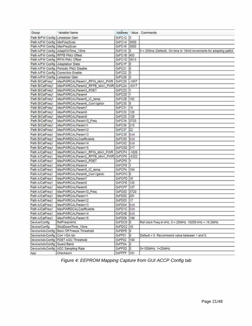
Figure 4: EEPROM Mapping Capture from GUI ACCP Config tab ................................................ 21
Figure 5: Guard Band Region ........................................................................................................ 26
Page 5/48
1. Introduction 1.1. Scope
This document provides the information necessary to develop the host software to communicate with the SC2200 via the Serial Peripheral Interface (SPI) interface.
1.2. Acronyms Acronyms Description
AGC Automatic Gain Control
EEPROM Electrically Erasable, Programmable, Read-Only Memory
EVB Evaluation Board
PAR Peak-to-Average Ratio
PVT Process, Voltage and Temperature.
RFFB RF Feedback
RFIN RF Input
RFOUT RF Output
RFPAL RF PA Linearization
SBW Signal Bandwidth
SPI Serial Peripheral Interface
SSN SPI Slave Select Enable
XTAL Crystal
1.3. Revision History
Revision Description
0.5 Preliminary version
0.8 Added instruction to read and write to PRAM Application parameters. Add Clear/Set Calibration and Soft
Reset commands.
Fix errors on Scratch mapping. Added example code for Convert16B_signed_SC2200. Updated EEPROM
write instructions from 64-bytes to 128-bytes per page.
0.9 Added AdaptOnTime_10ms parameter. Updated example codes.
1.0 Added Scratch and EEPROM/PRAM parameters.
1.1 Based on firmware 5.0.09.04, updated Clear/Set Calibration commands, EEPROM and Scratch mappings
and Matlab example codes. Added Info Stack and Clear Info Stack commands, 16-byte host message
examples and Performance tuning parameters.
1.2 Fixed some errors in RF status and PMU structures. Added host SPI command to read RFIN and RFFB
AGC and PMU values.
1.3 Fixed error in Info Stack offset. Updated performance tuning section and added section on performance
optimization with the guard band parameter.
Added clarification to read/write procedure to EEPROM.
1.4 General edits to remove requirement for NDA to access SC2200 collateral.
Page 6/48
1.4. References
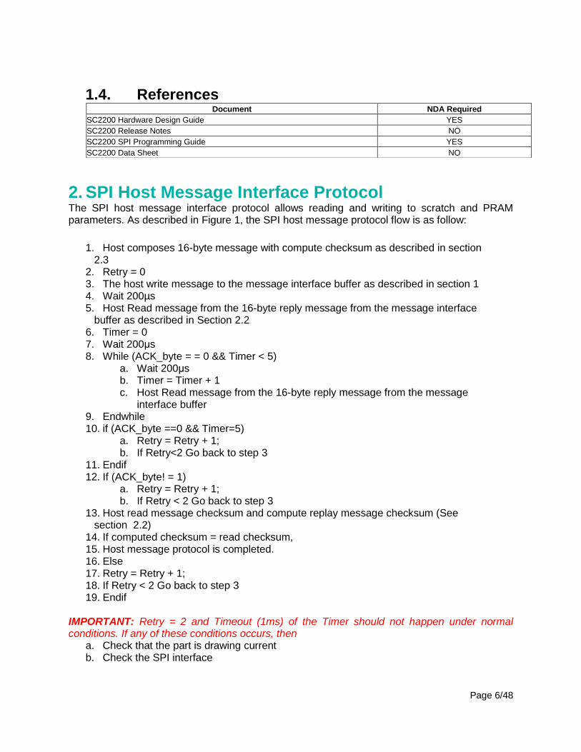
2. SPI Host Message Interface Protocol The SPI host message interface protocol allows reading and writing to scratch and PRAM parameters. As described in Figure 1, the SPI host message protocol flow is as follow:
1. Host composes 16-byte message with compute checksum as described in section 2.3
2. Retry = 0 3. The host write message to the message interface buffer as described in section 1 4. Wait 200µs 5. Host Read message from the 16-byte reply message from the message interface
buffer as described in Section 2.2 6. Timer = 0 7. Wait 200μs 8. While (ACK_byte = = 0 && Timer < 5)
a. Wait 200μs b. Timer = Timer + 1 c. Host Read message from the 16-byte reply message from the message
interface buffer 9. Endwhile 10. if (ACK_byte ==0 && Timer=5)
a. Retry = Retry + 1; b. If Retry<2 Go back to step 3
11. Endif 12. If (ACK_byte! = 1)
a. Retry = Retry + 1; b. If Retry < 2 Go back to step 3
13. Host read message checksum and compute replay message checksum (See section 2.2)
14. If computed checksum = read checksum, 15. Host message protocol is completed. 16. Else 17. Retry = Retry + 1; 18. If Retry < 2 Go back to step 3 19. Endif
IMPORTANT: Retry = 2 and Timeout (1ms) of the Timer should not happen under normal conditions. If any of these conditions occurs, then
a. Check that the part is drawing current b. Check the SPI interface
Document NDA Required
SC2200 Hardware Design Guide YES
SC2200 Release Notes NO
SC2200 SPI Programming Guide YES
SC2200 Data Sheet NO
Page 7/48
c. Try to increase the timer and the Retry limit until it is stable and let Maxim Integrated support team know.
Start
Compose 16-byte MSG
With computed CHK
Write MSG to MSG Buffer
Wait 200µs
Read MSG Buffer
ACK=0?
Read MSG + CHK
Timer<5
Compute CHK
over MSG
CHK match?DoneY
N
Y
Y
N
N
ACK=1?
Y
N
Figure 1. Host SPI Message Protocol Flow Diagram
Page 8/48
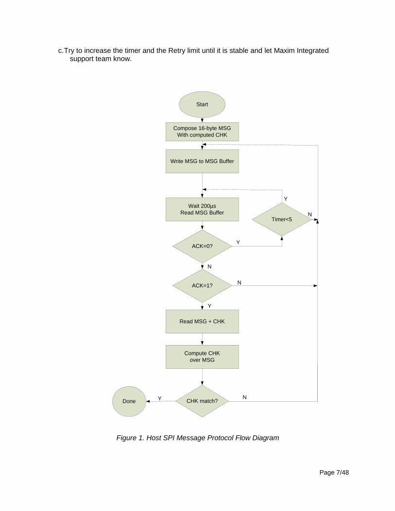
2.1. Host Write Operation to Message Interface Buffer The host writes the 16-byte message to the message interface buffer, as described in Table 1 and Figure 2. The Host 16-byte message structure is defined in section 2.3.
Table 1: Host Write Operation to Message Interface Buffer
Byte 0 1 2 3 to 18
Bits A15-A8 A7-A0 A19-A16 R/W bit
Value 20 40 20 Host Message Bytes 0 to 15
D6D7 D5 D4 D3 D2 D1 D0
Byte 0
HIGH IMPEDENCE
32 33 34 35 36 37 38 39
D5 D4 D3 D2 D1 D0
Byte 1
D7 D6
40 41 42 43 44 45 46 47
D5 D4 D3 D2 D1
Byte 4
D6 D6D7 D7 D5 D4 D3 D2 D1
Byte 15
D0 D0
HIGH IMPEDENCE
SSN
SDI
SDO
TA
A12 A1 A16
20 BIT ADDRESS
A15 A14 A13 A0 A19 A18 A17
R/W
BIT
0 1 2 3 14 15 16 21 22 23 24 25 26 27 28 29 3019 20SCLK 17 18 31
Figure 2: Host Write Operation to Message Interface
Host Sending on SDI
Page 9/48
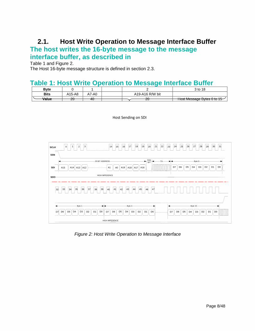
2.2. Host Read Operation from Message Interface Buffer The host read the 16-byte message reply from the Message Interface Buffer as described in Table 2 and Figure 3. The SC2200 16-byte reply message structure is defined in section 2.3.
Table 2: Host Read Operation from Message Interface Buffer Byte 0 1 2 3 to 18
Bits A15-A8 A7-A0 A19-A16 R/W bit
Value 20 40 2B SC2200 Message Reply Byte 0 to 15
0 1 2 3 14 15 16 21 22 23 24 25 26 27 28 29 30
HIGH IMPEDANCE
(pulled down on the board)
19 20
32 33 34 35 36 37 38 39
D5 D4 D3 D2 D1 D0
Byte 1
D7 D6
40 41 42 43 44 45 46 47
D5 D4 D3 D2 D1
Byte 2
D6 D6D7 D7 D5 D4 D3 D2 D1
Byte 15
D0 D0
SCLK
SSN
SDI
SDO
A12 A1 A16
20 BIT ADDRESS
A15 A14 A13 A0 A19
TA
D5 D4 D3 D2 D1
Byte 0
D7 D6 D0
A18 A17
17 18
R/W
BIT
31
*
S/F
BR
Figure 3: Host Read Operation from Message Interface
Host Sending on SDI SC2200 Responding on SDO
Page 10/48
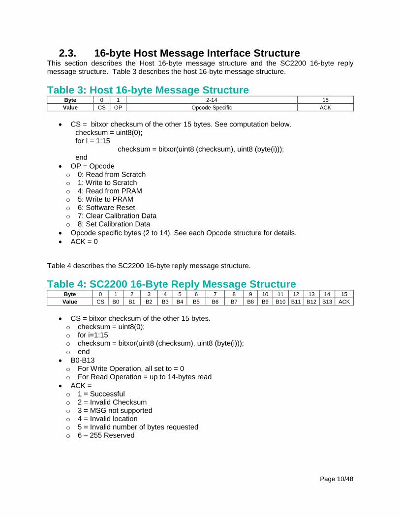
2.3. 16-byte Host Message Interface Structure This section describes the Host 16-byte message structure and the SC2200 16-byte reply message structure. Table 3 describes the host 16-byte message structure.
Table 3: Host 16-byte Message Structure Byte 0 1 2-14 15
Value CS OP Opcode Specific ACK
CS = bitxor checksum of the other 15 bytes. See computation below. checksum = uint8(0); for I = 1:15
checksum = bitxor(uint8 (checksum), uint8 (byte(i))); end
OP = Opcode o 0: Read from Scratch o 1: Write to Scratch o 4: Read from PRAM o 5: Write to PRAM o 6: Software Reset o 7: Clear Calibration Data o 8: Set Calibration Data
Opcode specific bytes (2 to 14). See each Opcode structure for details.
ACK = 0
Table 4 describes the SC2200 16-byte reply message structure.
Table 4: SC2200 16-Byte Reply Message Structure Byte 0 1 2 3 4 5 6 7 8 9 10 11 12 13 14 15
Value CS B0 B1 B2 B3 B4 B5 B6 B7 B8 B9 B10 B11 B12 B13 ACK
CS = bitxor checksum of the other 15 bytes. o checksum = uint8(0); o for i=1:15 o checksum = bitxor(uint8 (checksum), uint8 (byte(i))); o end
B0-B13 o For Write Operation, all set to = 0 o For Read Operation = up to 14-bytes read
ACK = o 1 = Successful o 2 = Invalid Checksum o 3 = MSG not supported o 4 = Invalid location o 5 = Invalid number of bytes requested o 6 – 255 Reserved
Page 11/48
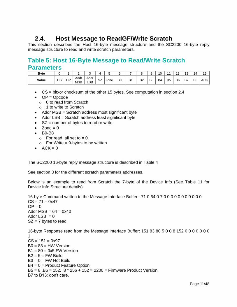
2.4. Host Message to ReadGF/Write Scratch This section describes the Host 16-byte message structure and the SC2200 16-byte reply message structure to read and write scratch parameters.
Table 5: Host 16-Byte Message to Read/Write Scratch Parameters
Byte 0 1 2 3 4 5 6 7 8 9 10 11 12 13 14 15
Value CS OP Addr
MSB
Addr
LSB SZ Zone B0 B1 B2 B3 B4 B5 B6 B7 B8 ACK
CS = bitxor checksum of the other 15 bytes. See computation in section 2.4
OP = Opcode o 0 to read from Scratch o 1 to write to Scratch
Addr MSB = Scratch address most significant byte
Addr LSB = Scratch address least significant byte
SZ = number of bytes to read or write
Zone = 0
B0-B8 o For read, all set to = 0 o For Write = 9-bytes to be written
ACK = 0
The SC2200 16-byte reply message structure is described in Table 4 See section 3 for the different scratch parameters addresses. Below is an example to read from Scratch the 7-byte of the Device Info (See Table 11 for Device Info Structure details) 16-byte Command written to the Message Interface Buffer: 71 0 64 0 7 0 0 0 0 0 0 0 0 0 0 0 CS = 71 = 0x47 OP = 0 Addr MSB = 64 = 0x40 Addr LSB = 0 SZ = 7 bytes to read 16-byte Response read from the Message Interface Buffer: 151 83 80 5 0 0 8 152 0 0 0 0 0 0 0 1 CS = 151 = 0x97 B0 = 83 = HW Version B1 = 80 = 0x5 FW Version B2 = 5 = FW Build B3 = 0 = FW Hot Build B4 = 0 = Product Feature Option B5 = 8 ,B6 = 152. 8 * 256 + 152 = 2200 = Firmware Product Version B7 to B13: don’t care.
Page 12/48
ACK = 1 = Successful
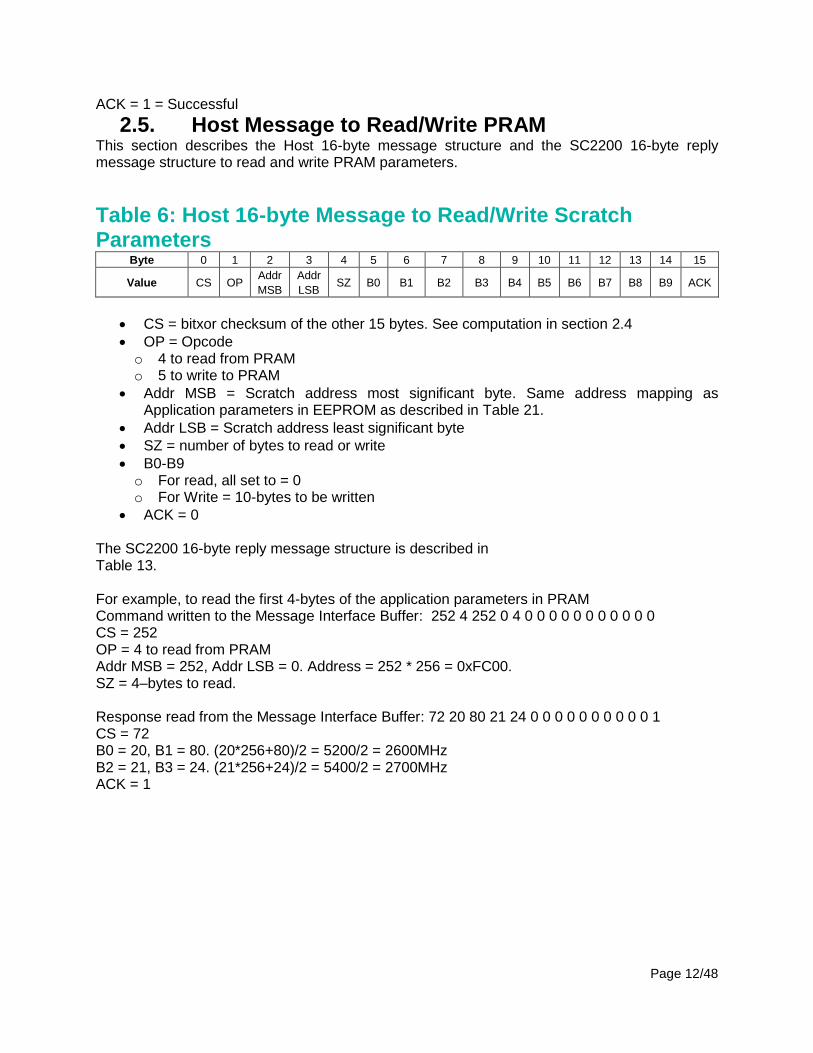
2.5. Host Message to Read/Write PRAM This section describes the Host 16-byte message structure and the SC2200 16-byte reply message structure to read and write PRAM parameters.
Table 6: Host 16-byte Message to Read/Write Scratch Parameters
Byte 0 1 2 3 4 5 6 7 8 9 10 11 12 13 14 15
Value CS OP Addr
MSB
Addr
LSB SZ B0 B1 B2 B3 B4 B5 B6 B7 B8 B9 ACK
CS = bitxor checksum of the other 15 bytes. See computation in section 2.4
OP = Opcode o 4 to read from PRAM o 5 to write to PRAM
Addr MSB = Scratch address most significant byte. Same address mapping as Application parameters in EEPROM as described in Table 21.
Addr LSB = Scratch address least significant byte
SZ = number of bytes to read or write
B0-B9 o For read, all set to = 0 o For Write = 10-bytes to be written
ACK = 0
The SC2200 16-byte reply message structure is described in Table 13. For example, to read the first 4-bytes of the application parameters in PRAM Command written to the Message Interface Buffer: 252 4 252 0 4 0 0 0 0 0 0 0 0 0 0 0 CS = 252 OP = 4 to read from PRAM Addr MSB = 252, Addr LSB = 0. Address = 252 * 256 = 0xFC00. SZ = 4–bytes to read. Response read from the Message Interface Buffer: 72 20 80 21 24 0 0 0 0 0 0 0 0 0 0 1 CS = 72 B0 = 20, B1 = 80. (20*256+80)/2 = 5200/2 = 2600MHz B2 = 21, B3 = 24. (21*256+24)/2 = 5400/2 = 2700MHz ACK = 1
Page 13/48
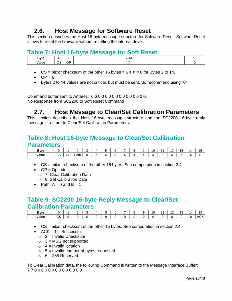
2.6. Host Message for Software Reset This section describes the Host 16-byte message structure for Software Reset. Software Reset allows to reset the firmware without resetting the internal driver.
Table 7: Host 16-byte Message for Soft Reset Byte 0 1 2-14 15
Value CS OP X 0
CS = bitxor checksum of the other 15 bytes = 6 if X = 0 for Bytes 2 to 14.
OP = 6
Bytes 2 to 14 values are not critical, but must be sent. So recommend using “0”
Command buffer sent to Antares: 6 6 0 0 0 0 0 0 0 0 0 0 0 0 0 0. No Response from SC2200 to Soft Reset Command
2.7. Host Message to Clear/Set Calibration Parameters This section describes the Host 16-byte message structure and the SC2200 16-byte reply message structure to Clear/Set Calibration Parameters.
Table 8: Host 16-byte Message to Clear/Set Calibration Parameters
Byte 0 1 2 3 4 5 6 7 8 9 10 11 12 13 14 15
Value CS OP Path 0 X X X X X X X X X X X 0
CS = bitxor checksum of the other 15 bytes. See computation in section 2.4
OP = Opcode o 7: Clear Calibration Data o 8: Set Calibration Data
Path: A = 0 and B = 1
Table 9: SC2200 16-byte Reply Message to Clear/Set Calibration Parameters
Byte 0 1 2 3 4 5 6 7 8 9 10 11 12 13 14 15
Value CS 0 0 0 0 0 0 0 0 0 0 0 0 0 0 ACK
CS = bitxor checksum of the other 15 bytes. See computation in section 2.4
ACK = 1 = Successful o 2 = Invalid Checksum o 3 = MSG not supported o 4 = Invalid location o 5 = Invalid number of bytes requested o 6 – 255 Reserved
To Clear Calibration data, the following Command is written to the Message Interface Buffer: 7 7 0 0 0 0 0 0 0 0 0 0 0 0 0 0
Page 14/48
with CS = 7 = OP = 7. Need to read Response from the Message Interface Buffer until the following is read: 1 1 0 0 0 0 0 0 0 0 0 0 0 0 0 1 To Set Calibration data, the following Command is written to the Message Interface Buffer: 8 8 0 0 0 0 0 0 0 0 0 0 0 0 0 0 with CS = 8 = OP = 8. Need to read Response from the Message Interface Buffer until the following is read: 1 0 0 0 0 0 0 0 0 0 0 0 0 0 0 1 IMPORTANT
a. It is recommended to Reset after Clear or Set Calibration (Hardware or SoftReset) b. Before sending Set Calibration data, please wait for acceptable performance.
Page 15/48
3. Global Scratch Parameters The host can read or write to the Global scratch parameters described in this section via the message protocol described in section 2.3. Please refer to Figure 1 for Host Flow Diagram and sections 7.4 and 7.5 for example code to read Scratch parameters.
Table 10: Global Scratch Parameters Available Via SPI Messages
Scratch
Address
(Hex)
Variable Name Description
4000 Device Info Device Info Structure. See Table 11 for detail.
403A FW Status Path A FW Status for path A. See Firmware Status Scratch Structure
Table 12 for detail.
4048 FW Status Path B FW Status for path B. See Firmware Status Scratch Structure
Table 12 for detail.
4056 RF Status Path A
RF Status Structure for path A. See RF Status Scratch
Structure
Table 13 for detail.
4068 RF Status Path B
RF Status Structure for path B. See RF Status Scratch
Structure
Table 13 for detail.
407A FW Debug Info Firmware Debugging information. See
Table 14
40B6 PMU Path B
Power Monitoring Unit Structure for Path B. See
PMU Scratch Structure
Table 19 for detail.
40C4 PMU Path A
Power Monitoring Unit Structure for Path A. See
PMU Scratch Structure
Table 19 for detail.
4110 IcTemp Path A Ic Temp for Path A
4176 IcTemp Path B Ic Temp for Path B
4330 Clear Info Stack Write 1 to clear the Info Stack. Once it reads back 0 Warnings
have been cleared
IMPORTANT
a. Global Scratch (also referred to Scratch) base address is 0x4000 b. It is also possible to use the SC2200 GUI ACCP Config tab to read the exact scratch
parameters (Scratch base address 0x4000 is not displayed in the GUI, only the offset).
Page 16/48
3.1. Device Info Scratch Structure Table 11: Device Info Structure
Offset (Hex) Size/Access Variable Name Description
00 UINT8 HW Version IC Version. Expected to be 83. Other values will generate
an error 29.
01 UINT8 FW Version FW version with a value of WX=0x50 displayed as 5.0
02 UINT8 FW Build FW Build number YY associated with FW version W.X with
values of WX=0x50 and YY=09 displayed as 5.0.09
03 UINT8 FW Hot Build
FW Hot Build number ZZ associated with FW version W.X
and FW Build YY with values of WX=0x50, YY=09 and
ZZ=04 displayed as 5.0.09.04
04 UINT8 Reserve Reserved (DO NOT CHANGE VALUES)
05 UINT16 Firmware Product Version Firmware Product Version. Expected to be 2200. Other
values will generate an error 31.
IMPORTANT - Do not write to these registers. See section 6.3 for the 16-byte message to the command buffer to read the Device Info Structure.
3.2. Firmware Status Scratch Structure Table 12: FW Status Structure
Offset (Hex) Size/Access Variable Name Description
000 UINT8 Status
Firmware Status
1 = VCO CAL
2 = PDET AGC
3 = PMU
4 = TRACK
5 = FROZEN
6 = FREQ_SCAN
7 = SHUTDOWN (If DeviceConfig.ShutDownTime_10ms > 0)
001 UINT8 Error Index
Index between 0 and 9 in Error stack array from FW
Debugging Information. See
Table 14 for detail.
002 UINT8 Info Index
Index between 0 and 9 in Info stack array from FW Debugging
Information. See
Table 14 for detail.
003 UINT16 Center Frequency 2xFrequency(MHz). Value of 0x1450 is 2600 MHz
005 UINT8 Signal Bandwidth 2xSignal Bandwidth(MHZ). Value of 0x28 is 20 MHz.
006 Reserved Reserved (DO NOT CHANGE VALUES)
007 INT16 Cost Function Current cost function power
IMPORTANT - It is recommended to periodically read the FW for general firmware status, no faster than every 100ms.
Page 17/48
3.3. RF Status Scratch Structure Table 13: RF Status Structure
Offset (Hex) Size/Access Variable Name Description
000 UINT8 Reserved Reserved (DO NOT CHANGE VALUES)
001 UINT8 RFFB AGC RFFB AGC value
002 UINT8 Reserved Reserved (DO NOT CHANGE VALUES)
003 INT16 RFIN AGC RFIN AGC value
3.4. Firmware Debugging Information Scratch Structure Table 14: Firmware Debugging Information Structure
Offset (Hex) Size/Access Variable Name Description
000 10x3 UINT8 ErrorStack Array with all error codes that have occurred
(circular, up to 10 errors)
01E 10x3 UINT8 InfoStack Array with all Information codes that have
occurred (circular, up to 10 Informations)
Table 15: Error Stack Structure Offset (Hex) Size/Access Variable Name Description
000 UINT8 ErrorCode Error Code. See Table 17 for error code
descriptions.
001 UINT8 Path 0 = Path A; 1 = Path B; 255 = General
002 UINT8 Reserved
Table 16: Info Stack Structure Offset (Hex) Size/Access Variable Name Description
000 UINT8 InfoCode Information Code. See Table 18 for info code
descriptions.
001 UINT8 Path 0 = Path A; 1 = Path B; 255 = General
002 UINT8 Reserved
Table 17: Error Code Descriptions Error Code Description
0 No error
3 Error 3 means EEPROM customer configuration parameter corruption. See EEPROM mapping for customer
configuration parameters in Table 21
9 Internal Temperature is too high (>140ºC)
10 Internal Temperature is too low (<-60 ºC)
29 If HW Version different than 83. See Table 11.
31 If Firmware Product Version different than 2200. See Table 11.
Page 18/48
Table 18: Information Code Descriptions Info Code Description
0 No Information
12
WatchDog Reset Event. If the 8051 microcontroller has reset at any given time due to a FW timeout
occurrence.
This only gets cleared with hardware reset or “Clear Info” command.
14
Max Calibration RFFB Power level is below -45dBm. Please make sure components on RFFB are assembled
properly. This info code will only be reported if system is calibrated with RFFB below -45dBm. This should
never happen under normal conditions.
16
Max Calibration RFIN Power level is below -30dBm. Please make sure components on RFIN are assembled
properly. This info code will only be reported if system is calibrated with RFIN below -30dBm. This should
never happen under normal conditions.
3.5. PMU Scratch Structure Table 19: PMU Structure
Offset (Hex) Size/Access Variable Name Description
000
001 INT16 RFFB RMS
RFFB RMS Power (dBm/10ms) over a 10ms measurement
window. Signed 6.10 signed dBN Value. See below for
conversion from dBN to dBm value.
002
005 Reserved Reserved (DO NOT CHANGE VALUES)
006
007 INT16 RFIN RMS
RFIN RMS Power (dBm/10ms) over a 10ms measurement
window. Signed 6.10 signed dBN Value. See below for
conversion from dBN to dBm value.
008
00B Reserved Reserved (DO NOT CHANGE VALUES)
00C
00D INT16 PA Gain
PA Gain = (RFFB RMS – RFIN RMS) Power (dBm/10ms) over a
10ms measurement window. Signed 6.10 signed dBN Value.
See below for conversion from dBN to dBm value.
Conversion from dBN to dBm as follow:
𝑃𝑑𝐵𝑚 =𝑑𝐵𝑁 ∗ 3.01
1024
Page 19/48
4. Reprogramming the EEPROM with Updated Firmware and Application Parameters
IMPORTANT - To reprogram the EEPROM with updated firmware and new application parameters, it is important to know the EEPROM mapping as described in Table 20 as the firmware download must start at address 0x0000 and not go over 0XFBFF. Additionally, the EEPROM addresses for application parameters are listed in Table 21. The same EEPROM read and write instructions described in sections 4.7 and 4.10 are used to upload new firmware or update the customer configuration parameters. IMPORTANT - The number of EEPROM erase/write cycles is limited to 1M.
4.1. EEPROM Mapping and Application Parameters Table 20: EEPROM Mapping
EEPROM
Addressed (Hex) Description
0000-FBFF
Download firmware starting at address 0x0000
Note: Firmware size may be smaller.
IMPORTANT - Do not write in the range; (end of firmware):0xFBFF
FC00-FFFF Application parameters. See Table 21 for detail.
Page 20/48
Table 21: EEPROM addresses for Application parameters EEPROM @
(Hex) Size (Hex) Variable Name Description
FC00
FC13 14 FwConfigPathB
Firmware Configuration Path B. See
Table 22 for details.
FC14
FC27 14 FwConfigPathA
Firmware Configuration Path A Structure. See
Table 22 for details.
FC28
FC8D 66 CAL1ParamPathB
Calibration Parameters for Path B. See
Table 24 for details.
FC8E-FDF3 Reserved Reserved (DO NOT CHANGE VALUES)
FCF4
FD59 66 CAL1ParamPathA
Calibration Parameters for Path A. See
Table 24 for details.
FD5A-FDBF Reserved Reserved (DO NOT CHANGE VALUES)
FDC0
FDC2 3 DeviceConfig
Device Configuration affects both Channel A and B. See
Table 23 for detail description.
FDC3-FEFD Reserved Reserved (DO NOT CHANGE VALUES)
FEFE
FF1B 1D AdvConfig
Advanced Device Configuration affects both channel A and B.
See for
Table 25 detail description.
FF1C-FFFE Reserved Reserved (DO NOT CHANGE VALUES)
FFFF UINT8 Checksum Checksum = XOR(FC00:FFFE). See section 7.2.
IMPORTANT
1. 16-bit values are Big-endian.
2. Address 0xFFFF checksum = XOR(FC00:FFFE)
If the checksum does not match, the firmware will issue an error 3 3. It is possible to also check the Application parameters EEPROM mapping with the
SC2200GUI ACCP Config tab.
Page 21/48
Figure 4: EEPROM Mapping Capture from GUI ACCP Config tab
Page 22/48
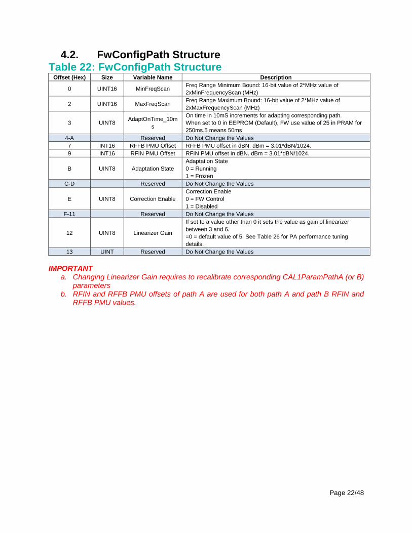
4.2. FwConfigPath Structure Table 22: FwConfigPath Structure
Offset (Hex) Size Variable Name Description
0 UINT16 MinFreqScan Freq Range Minimum Bound: 16-bit value of 2*MHz value of
2xMinFrequencyScan (MHz)
2 UINT16 MaxFreqScan Freq Range Maximum Bound: 16-bit value of 2*MHz value of
2xMaxFrequencyScan (MHz)
3 UINT8 AdaptOnTime_10m
s
On time in 10mS increments for adapting corresponding path.
When set to 0 in EEPROM (Default), FW use value of 25 in PRAM for
250ms.5 means 50ms
4-A Reserved Do Not Change the Values
7 INT16 RFFB PMU Offset RFFB PMU offset in dBN. dBm = 3.01*dBN/1024.
9 INT16 RFIN PMU Offset RFIN PMU offset in dBN. dBm = 3.01*dBN/1024.
B UINT8 Adaptation State
Adaptation State
0 = Running
1 = Frozen
C-D Reserved Do Not Change the Values
E UINT8 Correction Enable
Correction Enable
0 = FW Control
1 = Disabled
F-11 Reserved Do Not Change the Values
12 UINT8 Linearizer Gain
If set to a value other than 0 it sets the value as gain of linearizer
between 3 and 6.
=0 = default value of 5. See Table 26 for PA performance tuning
details.
13 UINT Reserved Do Not Change the Values
IMPORTANT
a. Changing Linearizer Gain requires to recalibrate corresponding CAL1ParamPathA (or B) parameters
b. RFIN and RFFB PMU offsets of path A are used for both path A and path B RFIN and RFFB PMU values.
Page 23/48
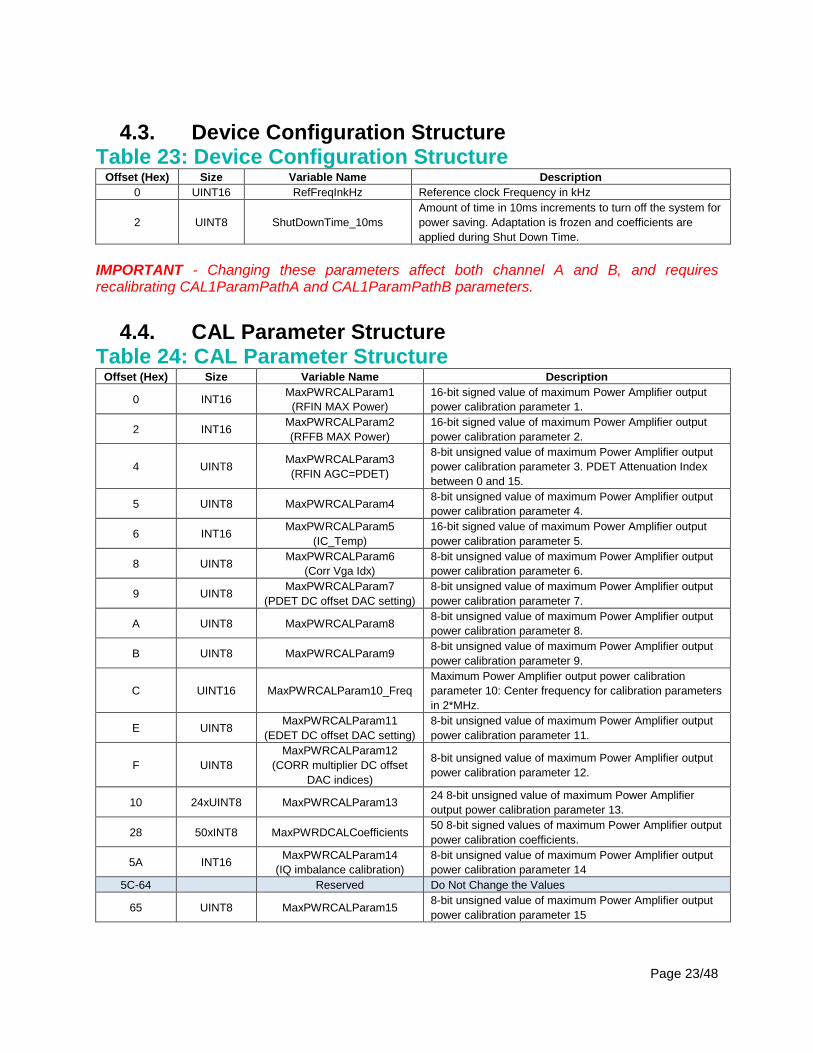
4.3. Device Configuration Structure Table 23: Device Configuration Structure
Offset (Hex) Size Variable Name Description
0 UINT16 RefFreqInkHz Reference clock Frequency in kHz
2 UINT8 ShutDownTime_10ms
Amount of time in 10ms increments to turn off the system for
power saving. Adaptation is frozen and coefficients are
applied during Shut Down Time.
IMPORTANT - Changing these parameters affect both channel A and B, and requires recalibrating CAL1ParamPathA and CAL1ParamPathB parameters.
4.4. CAL Parameter Structure
Table 24: CAL Parameter Structure Offset (Hex) Size Variable Name Description
0 INT16 MaxPWRCALParam1
(RFIN MAX Power)
16-bit signed value of maximum Power Amplifier output
power calibration parameter 1.
2 INT16 MaxPWRCALParam2
(RFFB MAX Power)
16-bit signed value of maximum Power Amplifier output
power calibration parameter 2.
4 UINT8 MaxPWRCALParam3
(RFIN AGC=PDET)
8-bit unsigned value of maximum Power Amplifier output
power calibration parameter 3. PDET Attenuation Index
between 0 and 15.
5 UINT8 MaxPWRCALParam4 8-bit unsigned value of maximum Power Amplifier output
power calibration parameter 4.
6 INT16 MaxPWRCALParam5
(IC_Temp)
16-bit signed value of maximum Power Amplifier output
power calibration parameter 5.
8 UINT8 MaxPWRCALParam6
(Corr Vga Idx)
8-bit unsigned value of maximum Power Amplifier output
power calibration parameter 6.
9 UINT8 MaxPWRCALParam7
(PDET DC offset DAC setting)
8-bit unsigned value of maximum Power Amplifier output
power calibration parameter 7.
A UINT8 MaxPWRCALParam8 8-bit unsigned value of maximum Power Amplifier output
power calibration parameter 8.
B UINT8 MaxPWRCALParam9 8-bit unsigned value of maximum Power Amplifier output
power calibration parameter 9.
C UINT16 MaxPWRCALParam10_Freq
Maximum Power Amplifier output power calibration
parameter 10: Center frequency for calibration parameters
in 2*MHz.
E UINT8 MaxPWRCALParam11
(EDET DC offset DAC setting)
8-bit unsigned value of maximum Power Amplifier output
power calibration parameter 11.
F UINT8
MaxPWRCALParam12
(CORR multiplier DC offset
DAC indices)
8-bit unsigned value of maximum Power Amplifier output
power calibration parameter 12.
10 24xUINT8 MaxPWRCALParam13 24 8-bit unsigned value of maximum Power Amplifier
output power calibration parameter 13.
28 50xINT8 MaxPWRDCALCoefficients 50 8-bit signed values of maximum Power Amplifier output
power calibration coefficients.
5A INT16 MaxPWRCALParam14
(IQ imbalance calibration)
8-bit unsigned value of maximum Power Amplifier output
power calibration parameter 14
5C-64 Reserved Do Not Change the Values
65 UINT8 MaxPWRCALParam15 8-bit unsigned value of maximum Power Amplifier output
power calibration parameter 15
Page 24/48
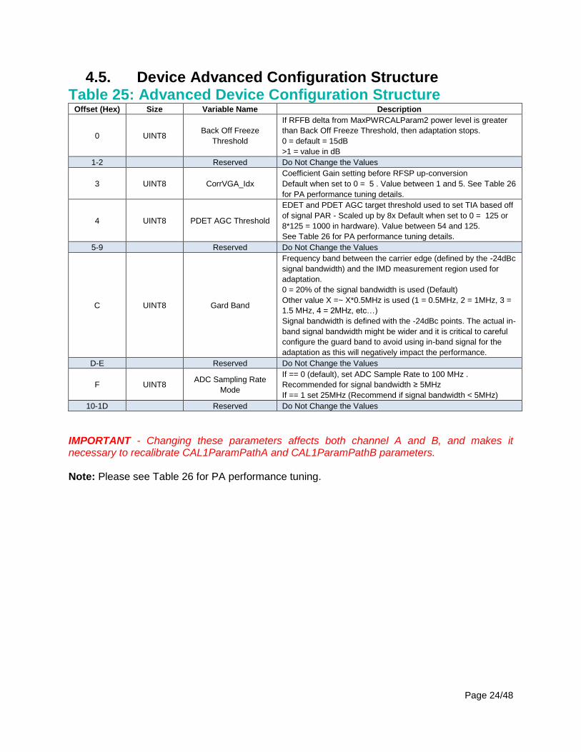
4.5. Device Advanced Configuration Structure Table 25: Advanced Device Configuration Structure
Offset (Hex) Size Variable Name Description
0 UINT8 Back Off Freeze
Threshold
If RFFB delta from MaxPWRCALParam2 power level is greater
than Back Off Freeze Threshold, then adaptation stops.
0 = default = 15dB
>1 = value in dB
1-2 Reserved Do Not Change the Values
3 UINT8 CorrVGA_Idx
Coefficient Gain setting before RFSP up-conversion
Default when set to 0 = 5 . Value between 1 and 5. See Table 26
for PA performance tuning details.
4 UINT8 PDET AGC Threshold
EDET and PDET AGC target threshold used to set TIA based off
of signal PAR - Scaled up by 8x Default when set to 0 = 125 or
8*125 = 1000 in hardware). Value between 54 and 125.
See Table 26 for PA performance tuning details.
5-9 Reserved Do Not Change the Values
C UINT8 Gard Band
Frequency band between the carrier edge (defined by the -24dBc
signal bandwidth) and the IMD measurement region used for
adaptation.
0 = 20% of the signal bandwidth is used (Default)
Other value X =~ X*0.5MHz is used (1 = 0.5MHz, 2 = 1MHz, 3 =
1.5 MHz, 4 = 2MHz, etc…)
Signal bandwidth is defined with the -24dBc points. The actual in-
band signal bandwidth might be wider and it is critical to careful
configure the guard band to avoid using in-band signal for the
adaptation as this will negatively impact the performance.
D-E Reserved Do Not Change the Values
F UINT8 ADC Sampling Rate
Mode
If == 0 (default), set ADC Sample Rate to 100 MHz .
Recommended for signal bandwidth ≥ 5MHz
If == 1 set 25MHz (Recommend if signal bandwidth < 5MHz)
10-1D Reserved Do Not Change the Values
IMPORTANT - Changing these parameters affects both channel A and B, and makes it necessary to recalibrate CAL1ParamPathA and CAL1ParamPathB parameters. Note: Please see Table 26 for PA performance tuning.
Page 25/48
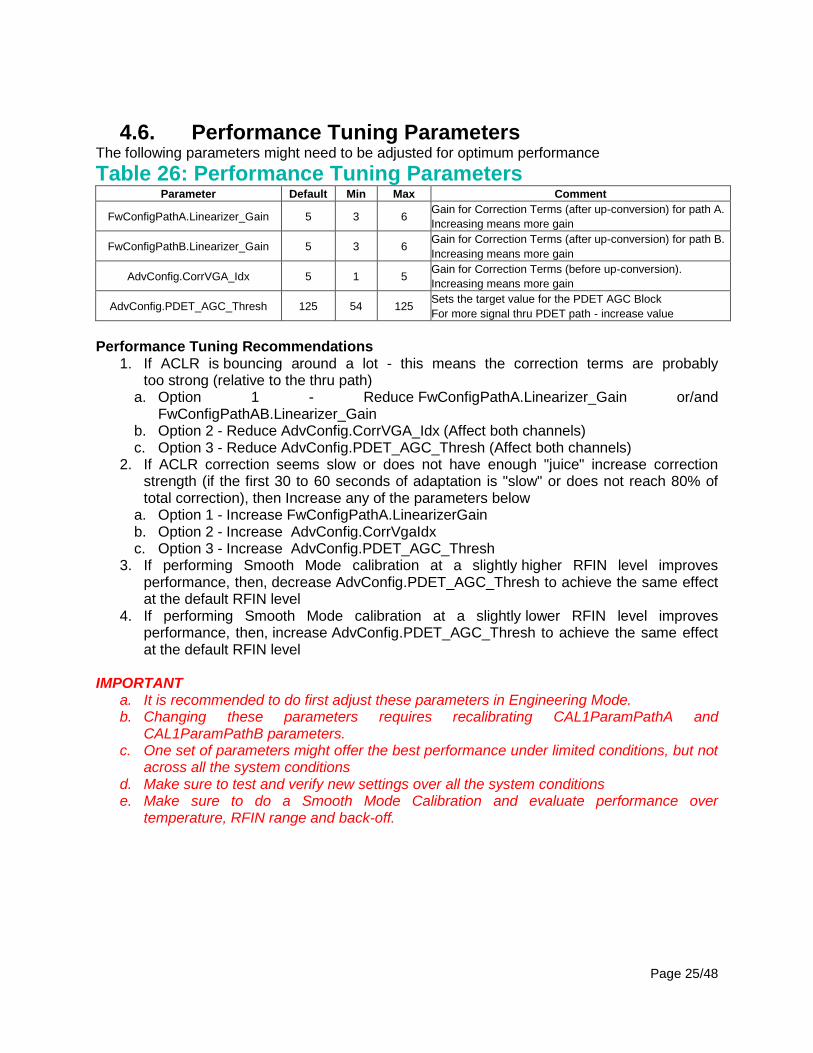
4.6. Performance Tuning Parameters The following parameters might need to be adjusted for optimum performance
Table 26: Performance Tuning Parameters Parameter Default Min Max Comment
FwConfigPathA.Linearizer_Gain 5 3 6 Gain for Correction Terms (after up-conversion) for path A.
Increasing means more gain
FwConfigPathB.Linearizer_Gain 5 3 6 Gain for Correction Terms (after up-conversion) for path B.
Increasing means more gain
AdvConfig.CorrVGA_Idx 5 1 5 Gain for Correction Terms (before up-conversion).
Increasing means more gain
AdvConfig.PDET_AGC_Thresh 125 54 125 Sets the target value for the PDET AGC Block
For more signal thru PDET path - increase value
Performance Tuning Recommendations
1. If ACLR is bouncing around a lot - this means the correction terms are probably too strong (relative to the thru path)
a. Option 1 - Reduce FwConfigPathA.Linearizer_Gain or/and FwConfigPathAB.Linearizer_Gain
b. Option 2 - Reduce AdvConfig.CorrVGA_Idx (Affect both channels) c. Option 3 - Reduce AdvConfig.PDET_AGC_Thresh (Affect both channels)
2. If ACLR correction seems slow or does not have enough "juice" increase correction strength (if the first 30 to 60 seconds of adaptation is "slow" or does not reach 80% of total correction), then Increase any of the parameters below
a. Option 1 - Increase FwConfigPathA.LinearizerGain b. Option 2 - Increase AdvConfig.CorrVgaIdx c. Option 3 - Increase AdvConfig.PDET_AGC_Thresh
3. If performing Smooth Mode calibration at a slightly higher RFIN level improves performance, then, decrease AdvConfig.PDET_AGC_Thresh to achieve the same effect at the default RFIN level
4. If performing Smooth Mode calibration at a slightly lower RFIN level improves performance, then, increase AdvConfig.PDET_AGC_Thresh to achieve the same effect at the default RFIN level
IMPORTANT a. It is recommended to do first adjust these parameters in Engineering Mode. b. Changing these parameters requires recalibrating CAL1ParamPathA and
CAL1ParamPathB parameters. c. One set of parameters might offer the best performance under limited conditions, but not
across all the system conditions d. Make sure to test and verify new settings over all the system conditions e. Make sure to do a Smooth Mode Calibration and evaluate performance over
temperature, RFIN range and back-off.

Page 26/48
4.7. Meeting Spectral Emission Limits Very Close to Carrier
The guard band is the frequency band between the carrier edge (defined by the -24dBc signal bandwidth) and the IMD measurement region used for adaptation as illustrated in Figure 5. If a particular Spectral Emission Mask (SEM) specification requires that distortion very close to the carrier be reduced more than it is with the default settings, then use of the guard band parameter may help to achieve the required specification. The default setting is for the guard band region to be 20% of the carrier bandwidth. For 20 MHz carriers, this means that the distortion in the 4MHz region on either side of the carrier is ignored. There will be some reduction of the distortion at 1MHz offset due to the linearizer acting on the IM3 distortion that it is considering, but potentially more reduction can be achieved at the 1MHz offset point by reducing the guard band region. It is not a good idea to use a value of 1 since carrier power may be inadvertently included in the distortion, but a value of 2 should be safe. Each unit represents approximately 0.5MHz.
24 dBc BW
24 dB
Guard
Band
UPPER Out-Of-Band
Adaptation Region
LOWER Out-Of-Band
Adaptation Region
Guard Band Region
Guard
Band
Figure 5: Guard Band Region
For a narrowband carrier such as 5MHz, changing the Guard Band parameter will likely not help,
Page 27/48
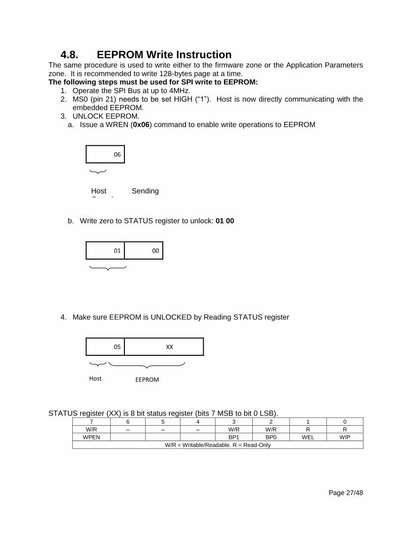
4.8. EEPROM Write Instruction The same procedure is used to write either to the firmware zone or the Application Parameters zone. It is recommended to write 128-bytes page at a time. The following steps must be used for SPI write to EEPROM:
1. Operate the SPI Bus at up to 4MHz. 2. MS0 (pin 21) needs to be set HIGH (“1”). Host is now directly communicating with the
embedded EEPROM. 3. UNLOCK EEPROM.
a. Issue a WREN (0x06) command to enable write operations to EEPROM
06
b. Write zero to STATUS register to unlock: 01 00
01 00
4. Make sure EEPROM is UNLOCKED by Reading STATUS register
05 XX
STATUS register (XX) is 8 bit status register (bits 7 MSB to bit 0 LSB). 7 6 5 4 3 2 1 0
W/R – – – W/R W/R R R
WPEN BP1 BP0 WEL WIP
W/R = Writable/Readable. R = Read-Only
Host Sending Opcode
Host Sending Opcode
EEPROM response
Host Sending Opcode
Page 28/48
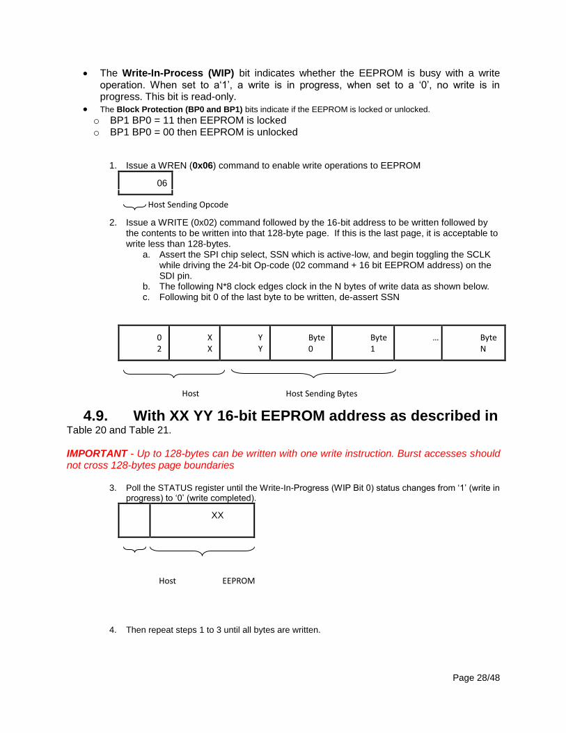
The Write-In-Process (WIP) bit indicates whether the EEPROM is busy with a write operation. When set to a‘1’, a write is in progress, when set to a ‘0’, no write is in progress. This bit is read-only.
The Block Protection (BP0 and BP1) bits indicate if the EEPROM is locked or unlocked. o BP1 BP0 = 11 then EEPROM is locked o BP1 BP0 = 00 then EEPROM is unlocked
1. Issue a WREN (0x06) command to enable write operations to EEPROM
06
2. Issue a WRITE (0x02) command followed by the 16-bit address to be written followed by the contents to be written into that 128-byte page. If this is the last page, it is acceptable to write less than 128-bytes.
a. Assert the SPI chip select, SSN which is active-low, and begin toggling the SCLK while driving the 24-bit Op-code (02 command + 16 bit EEPROM address) on the SDI pin.
b. The following N*8 clock edges clock in the N bytes of write data as shown below. c. Following bit 0 of the last byte to be written, de-assert SSN
02
XX
YY
Byte0
Byte1
… ByteN
4.9. With XX YY 16-bit EEPROM address as described in Table 20 and Table 21. IMPORTANT - Up to 128-bytes can be written with one write instruction. Burst accesses should not cross 128-bytes page boundaries
3. Poll the STATUS register until the Write-In-Progress (WIP Bit 0) status changes from ‘1’ (write in progress) to ‘0’ (write completed).
05
XX
4. Then repeat steps 1 to 3 until all bytes are written.
Host Sendi
Host Sending Bytes
Host Sending Opcode
Host Sending Opcode
EEPROM response
Page 29/48
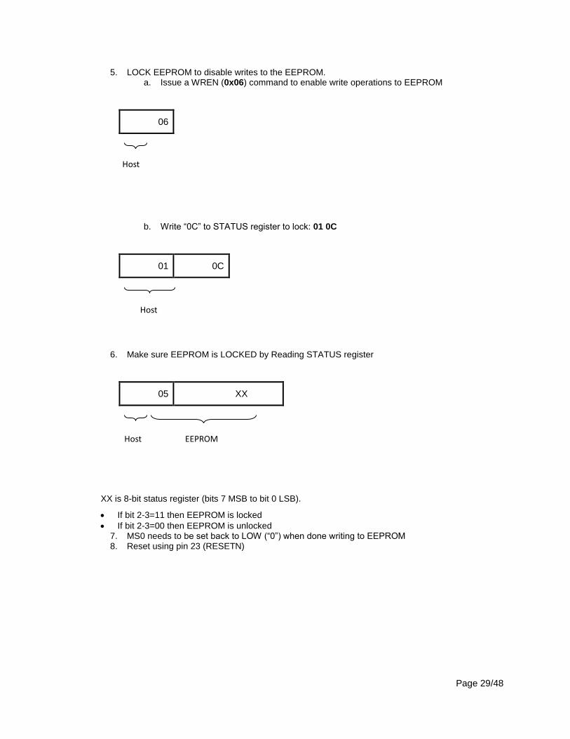
5. LOCK EEPROM to disable writes to the EEPROM. a. Issue a WREN (0x06) command to enable write operations to EEPROM
06
b. Write “0C” to STATUS register to lock: 01 0C
01 0C
6. Make sure EEPROM is LOCKED by Reading STATUS register
05 XX
XX is 8-bit status register (bits 7 MSB to bit 0 LSB).
If bit 2-3=11 then EEPROM is locked
If bit 2-3=00 then EEPROM is unlocked 7. MS0 needs to be set back to LOW (“0”) when done writing to EEPROM 8. Reset using pin 23 (RESETN)
Host Sending Opcode
Host Sending Opcode
EEPROM response
Host Sending Opcode
Page 30/48
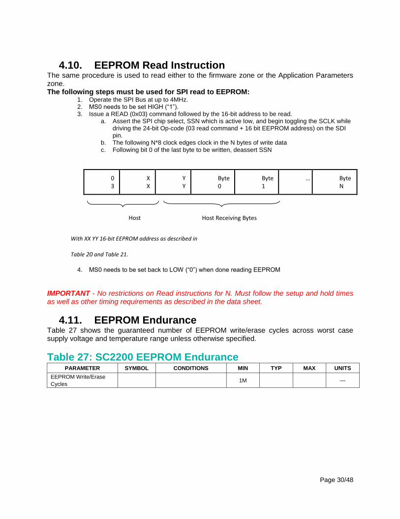
4.10. EEPROM Read Instruction The same procedure is used to read either to the firmware zone or the Application Parameters zone. The following steps must be used for SPI read to EEPROM:
1. Operate the SPI Bus at up to 4MHz. 2. MS0 needs to be set HIGH (“1”). 3. Issue a READ (0x03) command followed by the 16-bit address to be read.
a. Assert the SPI chip select, SSN which is active low, and begin toggling the SCLK while driving the 24-bit Op-code (03 read command + 16 bit EEPROM address) on the SDI pin.
b. The following N*8 clock edges clock in the N bytes of write data c. Following bit 0 of the last byte to be written, deassert SSN
03
XX
YY
Byte0
Byte1
… ByteN
With XX YY 16-bit EEPROM address as described in
Table 20 and Table 21.
4. MS0 needs to be set back to LOW (“0”) when done reading EEPROM
IMPORTANT - No restrictions on Read instructions for N. Must follow the setup and hold times as well as other timing requirements as described in the data sheet.
4.11. EEPROM Endurance Table 27 shows the guaranteed number of EEPROM write/erase cycles across worst case supply voltage and temperature range unless otherwise specified.
Table 27: SC2200 EEPROM Endurance PARAMETER SYMBOL CONDITIONS MIN TYP MAX UNITS
EEPROM Write/Erase
Cycles 1M
—
Host Sendi
Host Receiving Bytes
Page 31/48
5. PRAM Application Parameters All the EEPROM Application parameters defined in Table 21 are loaded to PRAM at boot-up after power on or after Reset. Section 2.5 described how to read back all the application parameters from PRAM after boot-up and how to dynamically change some of these parameters by writing to PRAM. IMPORTANT - The Application parameters checksum is only checked when loaded from EEPROM to PRAM. So when changing parameters in PRAM, it is not required to update the checksum parameters.
5.1. To Enable/Disable Correction with PRAM Parameter To disable correction, the following command is written to the Message Interface Buffer: 247 5 252 14 1 1 0 0 0 0 0 0 0 0 0 0 CS = 247 OP = 5 to write to PRAM Addr MSB = 252, Addr LSB = 14. Address = 252*256 +14 = 0xFC0E. SZ = 1–bytes to write. B0 = 1 Response read from the Message Interface Buffer: 1 0 0 0 0 0 0 0 0 0 0 0 0 0 0 1 CS = 1, ACK = 1 for successful write To enable correction, the following command is written to the Message Interface Buffer: 246 5 252 14 1 0 0 0 0 0 0 0 0 0 0 0 CS = 246 OP = 5 to write to PRAM Addr MSB = 252, Addr LSB = 14. Address = 252*256 +14 = 0xFC0E. SZ = 1–bytes to write. B0 = 0 Response read from the Message Interface Buffer: 1 0 0 0 0 0 0 0 0 0 0 0 0 0 0 1 CS = 1, ACK = 1 for successful write
Page 32/48
5.2. To Freeze/UnFreeze Adaptation with PRAM Parameter
To freeze adaptation, the following command is written to the Message Interface Buffer: 242 5 252 11 1 1 0 0 0 0 0 0 0 0 0 0 CS = 242 OP = 5 to write to PRAM Addr MSB = 252, Addr LSB = 11. Address = 252 * 256 +11 = 0xFC0B. SZ = 1–bytes to write. B0 = 1 Response read from the Message Interface Buffer: 1 0 0 0 0 0 0 0 0 0 0 0 0 0 0 1 CS = 1, ACK = 1 for successful write To unfreeze adaptation, the following command is written to the Message Interface Buffer: 243 5 252 11 1 0 0 0 0 0 0 0 0 0 0 0 CS = 243 OP = 5 to Write to PRAM Addr MSB = 252, Addr LSB = 11. Address = 252*256 +11 = 0xFC0B. SZ = 1–bytes to write. B0 = 0 Response read from the Message Interface Buffer: 1 0 0 0 0 0 0 0 0 0 0 0 0 0 0 1 CS = 1, ACK = 1 for successful write
Page 33/48
5.3. To Read back Adaptation State and Correction Enable from PRAM
To read back the adaptation state and correction enable status, the following command is written to the Message Interface Buffer: 247 4 252 11 4 0 0 0 0 0 0 0 0 0 0 0 CS = 247, OP = 4 to read from PRAM Addr MSB = 252, Addr LSB = 11. Address = 252 * 256 + 11 = 0xFC0B. SZ = 4–bytes to read Response read from the Message Interface Buffer: 1 1 0 0 1 0 0 0 0 0 0 0 0 0 0 1 CS = 1 B0 = 1 = Adaptation State = Frozen B1= B2 = 0 B3 = 1 = Correction Enable = Disabled ACK = 1 = Successful read. If only the Correction Enable status is read, then the following command is written to the Message Interface Buffer: 247 4 252 14 1 0 0 0 0 0 0 0 0 0 0 0 CS=247, OP = 4 to read from PRAM Addr MSB = 252, Addr LSB = 14. Address = 252*256 +14 = 0xFC0E. SZ = 1–bytes to read Then the response read from the Message Interface Buffer is: 243 1 252 14 1 0 0 0 0 0 0 0 0 0 0 1 CS = 243 B0 = 1 = Correction Enable = Disabled Please note that since only-byte is read, B1, B2 and B3 are not written from SC2200 and still contain part of the host command written to the message buffer.
Page 34/48
6. 16-byte Host Message Interface Examples 6.1. SC2200_Clear_Calibration
To Clear Calibration for Path A (See section 2.7 for command detail and section [errorFlag] = SC2200_Clear_Calibration( d, 0) Command Buffer sent to SC2200: 7 7 0 0 0 0 0 0 0 0 0 0 0 0 0 0 (Try 0) Buffer read from SC2200: 0 0 0 0 0 0 0 0 0 0 0 0 0 0 0 255 … (Try 33) Buffer read from SC2200: 0 0 0 0 0 0 0 0 0 0 0 0 0 0 0 255 (Try 34) Buffer read from SC2200: 1 0 0 0 0 0 0 0 0 0 0 0 0 0 0 1 errorFlag = 0 IMPORTANT – ACK = 1, this means the read was successful and data is valid. It is critical to wait for ACK=1 before reading the response. 255 means that the response is not ready yet.
To Clear Calibration for Path B [errorFlag] = SC2200_Clear_Calibration( d, 1) Command buffer sent to SC2200: 6 7 1 0 0 0 0 0 0 0 0 0 0 0 0 0 (Try 0) Buffer read from SC2200: 0 0 0 0 0 0 0 0 0 0 0 0 0 0 0 255 (Try 1) Buffer read from SC2200: 0 0 0 0 0 0 0 0 0 0 0 0 0 0 0 255 … (Try 33) Buffer read from SC2200: 0 0 0 0 0 0 0 0 0 0 0 0 0 0 0 255 (Try 34) Buffer read from SC2200: 1 0 0 0 0 0 0 0 0 0 0 0 0 0 0 1 errorFlag = 0
6.2. SC2200_Set_Calibration To Set Calibration for Path A: [errorFlag] = SC2200_Set_Calibration( d, 0) Command buffer sent to SC2200: 8 8 0 0 0 0 0 0 0 0 0 0 0 0 0 0 (Try 0) Buffer read from SC2200: 0 0 0 0 0 0 0 0 0 0 0 0 0 0 0 255 (Try 1) Buffer read from SC2200: 0 0 0 0 0 0 0 0 0 0 0 0 0 0 0 255 … (Try 33) Buffer read from SC2200: 0 0 0 0 0 0 0 0 0 0 0 0 0 0 0 255 (Try 34) Buffer read from SC2200: 1 0 0 0 0 0 0 0 0 0 0 0 0 0 0 1 errorFlag = 0 IMPORTANT – ACK = 1, this means the read was successful and data is valid. It is critical to wait for ACK = 1 before reading the response. 255 means that the response is not ready yet. To Set Calibration for Path B: [errorFlag] = SC2200_Set_Calibration( d, 1) Command buffer sent to SC2200: 9 8 1 0 0 0 0 0 0 0 0 0 0 0 0 0 (Try 0) Buffer read from SC2200: 0 0 0 0 0 0 0 0 0 0 0 0 0 0 0 255 (Try 1) Buffer read from SC2200: 0 0 0 0 0 0 0 0 0 0 0 0 0 0 0 255 … (Try 33) Buffer read from SC2200: 0 0 0 0 0 0 0 0 0 0 0 0 0 0 0 255 (Try 34) Buffer read from SC2200: 1 0 0 0 0 0 0 0 0 0 0 0 0 0 0 1 errorFlag = 0
Page 35/48
6.3. Reading Device Information from Scratch When using the Matlab routine described in section 7.4 to read the device info structure (defined in Table 11), the following commands are exchanged: Command buffer sent to SC2200: 71 0 64 0 7 0 0 0 0 0 0 0 0 0 0 0 (Try 0) Buffer read from SC2200: 159 83 80 9 4 0 8 152 0 0 0 0 0 0 0 1 Device_Information = FirmwareProductVersion: 2200 = 8*256+152 HW_Version: 83 FW_Version: '50' (0x50= 80 in decimal) FW_Build: [9 4]
6.4. Reading Path A/B FW Status from Scratch See SC2200_Get_Paths_Status Matlab example code in section 7.6. % With No RF signal [errFlag, FwStatusPathA] = d.msg.ReadXdata(hex2dec('4000')+58, 0, 9) Command buffer sent to SC2200: 115 0 64 58 9 0 0 0 0 0 0 0 0 0 0 0 (Try 0) Buffer read from SC2200: 79 5 0 1 21 24 204 0 239 100 0 0 0 0 0 1 FwStatusPathA = [5 0 1 21 24 204 0 239 100] PathA.FwStatus_State = 5 = 'FROZEN' PathA.FwStatus_ErrorIndex = 0 = No Errors PathA.FwStatus_InfoIndex= 1 PathA.FwStatus_CenterFrequency = (21*256+24)/2 = 2700MHz PathA.FwStatus_SignalBW = (204/2) = 102 MHz (Means no RF signal is detected) PathA.FwStatus_CostFunction= Convert16B_signed_SC2200(239*256+100)=-4221 % With RF signal, Path A with 20MHz LTE [errFlag, FwStatusPathA] = d.msg.ReadXdata(hex2dec('4000')+58, 0, 9) Command buffer sent to SC2200: 115 0 64 58 9 0 0 0 0 0 0 0 0 0 0 0 (Try 0) Buffer read from SC2200: 3 4 0 0 17 248 39 0 182 126 0 0 0 0 0 1 FwStatusPathA = [4 0 0 17 248 39 0 182 126] PathA.FwStatus_State = 4 = 'TRACK' PathA.FwStatus_ErrorIndex = 0 = No Error PathA.FwStatus_InfoIndex= 0 = No Infor PathA.FwStatus_CenterFrequency = (17*256+248)/2 = 2300MHz PathA.FwStatus_SignalBW = (39/2) = 19.5 MHz PathA.FwStatus_CostFunction= Convert16B_signed_SC2200(182*256+126)= -18818 % With RF signal, Path B with 20MHz LTE [errFlag, FwStatusPathB] = d.msg.ReadXdata(hex2dec('4000')+72, 0, 9) Command buffer sent to SC2200: 1 0 64 72 9 0 0 0 0 0 0 0 0 0 0 0 (Try 0) Buffer read from SC2200: 220 4 0 0 17 248 39 0 207 216 0 0 0 0 0 1 FwStatusPathB = [4 0 0 17 248 39 0 207 216] PathB.FwStatus_State = 4 = 'TRACK' PathB.FwStatus_ErrorIndex = 0 = No Error PathB.FwStatus_InfoIndex= 0 = No Infor PathB.FwStatus_CenterFrequency = (17 * 256 + 248)/2 = 2300MHz PathB.FwStatus_SignalBW = (39/2) = 19.5MHz PathB.FwStatus_CostFunction = Convert16B_signed_SC2200(207*256+216) = -12328
Page 36/48
6.5. Reading Device FW Debug Information from Scratch
To read the first element of the Error Stack (Index=0) [errFlag, ErrorStack] = d.msg.ReadXdata(hex2dec('407A'), 0, 2); Command buffer sent to SC2200: 56 0 64 122 2 0 0 0 0 0 0 0 0 0 0 0 (Try 0) Buffer read from SC2200: 1 0 0 0 0 0 0 0 0 0 0 0 0 0 0 1 Device_FW_Debug.ErrorStack_error(0) = 0 %No error Device_FW_Debug.ErrorStack_path(0) = 0 % Path A by default if No error To read the first element of the Info Stack (Index=0) [errFlag, InfoStack] = d.msg.ReadXdata(hex2dec('4098'), 0, 2); Command buffer sent to SC2200: 218 0 64 152 2 0 0 0 0 0 0 0 0 0 0 0 (Try 0) Buffer read from SC2200: 15 14 0 0 0 0 0 0 0 0 0 0 0 0 0 1 Device_FW_Debug.InfoStack_info(0) = 14 % Path A was calibrated with no RF signal on RFFB Device_FW_Debug.ErrorStack_path(0) = 0 % Path A To read the second element of the Info Stack (Index=1) [errFlag, InfoStack] = d.msg.ReadXdata(1*3+hex2dec('4098'), 0, 2); Command buffer sent to SC2200: 217 0 64 155 2 0 0 0 0 0 0 0 0 0 0 0 (Try 0) Buffer read from SC2200: 17 16 0 0 0 0 0 0 0 0 0 0 0 0 0 1 Device_FW_Debug.InfoStack_info(0) = 16 % Path A was calibrated with no RF signal on RFIN Device_FW_Debug.ErrorStack_path(0) = 0 % Path A To read the third element of the Info Stack (Index=2) [errFlag, InfoStack] = d.msg.ReadXdata(2*3+hex2dec('4098'), 0, 2); Command buffer sent to SC2200: 220 0 64 158 2 0 0 0 0 0 0 0 0 0 0 0 (Try 0) Buffer read from SC2200: 14 14 1 0 0 0 0 0 0 0 0 0 0 0 0 1 Device_FW_Debug.InfoStack_info(0) = 14 % Path B was calibrated with no RF signal on RFFB Device_FW_Debug.ErrorStack_path(0) = 1 % Path B
6.6. Clear Info Stack To clear Info Stack, write to Global Scratch parameter at address 0x330 See section 2.4 for exact command description to write to Scratch errFlag = d.msg.WriteXdata(hex2dec('4330'),0,1); %Write 1 to Global Scratch address 0x330 Command buffer sent to SC2200: 114 1 67 48 1 0 1 0 0 0 0 0 0 0 0 0 (Try 0) Buffer read from SC2200: 1 0 0 0 0 0 0 0 0 0 0 0 0 0 0 1 errFlag = 0 %Clear successful.
Page 37/48
6.7. Read RFIN and RFFB AGC Values Using the Matlab example code described in section 7.5 to read the AGC values. [errFlag, RfStatusPathA] = d.msg.ReadXdata(hex2dec('4000')+86, 0, 5); Command buffer sent to SC2200: 19 0 64 86 5 0 0 0 0 0 0 0 0 0 0 0 (Try 0) Buffer read from SC2200: 11 17 26 0 0 1 0 0 0 0 0 0 0 0 0 1 PathA.RfStatus_RFFB_AGC= RfStatusPathA(2) = 26 PathA.RfStatus_RFIN_AGC= RfStatusPathA(4)*256+RfStatusPathA(5) = 0*256+1=1 Similarly on Path B [errFlag, RfStatusPathB] = d.msg.ReadXdata(hex2dec('4000')+104, 0, 5); Command buffer sent to SC2200: 45 0 64 104 5 0 0 0 0 0 0 0 0 0 0 0 (Try 0) Buffer read from SC2200: 6 17 23 0 0 1 0 0 0 0 0 0 0 0 0 1 PathB.RfStatus_RFFB_AGC= RfStatusPathB(2) = 23 PathB.RfStatus_RFIN_AGC= RfStatusPathB(4)*256+RfStatusPathB(5) = 0*256+1= 1
6.8. Read RFIN and RFFB PMU Values Using the Matlab example code described in section 7.5 to read the PMU values. [errFlag, PMU_pathA] = d.msg.ReadXdata(hex2dec('4000')+196, 0, 14); Command buffer sent to SC2200: 138 0 64 196 14 0 0 0 0 0 0 0 0 0 0 0 (Try 0) Buffer read from SC2200: 15 234 167 0 0 0 0 235 61 0 0 0 0 255 106 1 IMPORTANT – ACK = 1, this means the read was successful and data is valid. It is critical to wait for ACK = 1 before reading the response. PathA.PMU_RFFB = round(30.1*Convert16B_signed_SC2200(double(PMU_pathA(1))*256+double(PMU_pathA(2)))/1024)/10 = PathA.PMU_RFFB = round(30.1*Convert16B_signed_SC2200(double(234)*256+double(167))/1024)/10 = -16.2dBm PathA.PMU_RFIN = round(30.1*Convert16B_signed_SC2200(double(PMU_pathA(7))*256+double(PMU_pathA(8)))/1024)/10 = PathA.PMU_RFIN = round(30.1*Convert16B_signed_SC2200(double(235)*256+double(61))/1024)/10 = -15.6dBm Similarly on Path B [errFlag, PMU_pathB] = d.msg.ReadXdata(hex2dec('4000')+182, 0, 14); Command buffer sent to SC2200: 248 0 64 182 14 0 0 0 0 0 0 0 0 0 0 0 (Try 0) Buffer read from SC2200: 1 235 239 0 0 0 0 235 198 0 0 0 0 0 41 1 PathB.PMU_RFFB = round(30.1*Convert16B_signed_SC2200(double(PMU_pathB(1))*256+double(PMU_pathB(2)))/1024)/10 = round(30.1*Convert16B_signed_SC2200(double(235)*256+double(239))/1024)/10 = -15.1dBm PathB.PMU_RFIN = round(30.1*Convert16B_signed_SC2200(double(PMU_pathB(7))*256+double(PMU_pathB(8)))/1024)/10 = round(30.1*Convert16B_signed_SC2200(double(235)*256+double(198))/1024)/10 = -15.2dBm
Page 38/48
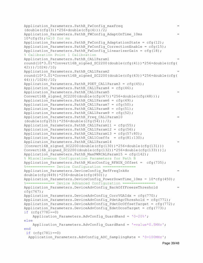
7. Matlab Example Codes 7.1. SC2200_Read_ApplicationParameters (From
EEPROM) function [Application_Parameters]=
SC2200_Read_customerConfigParameters(d)
cfg = d.EEPROM.EEPROM.Read(hex2dec('FC00'),1024)
%============= Path A ===============
% FW Configuration
Application_Parameters.PathA_FwConfig_minFreq =
(double(cfg(21))*256+double(cfg(22)))/2;
Application_Parameters.PathA_FwConfig_maxFreq =
(double(cfg(23))*256+double(cfg(24)))/2;
Application_Parameters.PathA_FwConfig_AdaptOnTime_10ms =
10*cfg(25);%x10 for ms
Application_Parameters.PathA_FwConfig_AdaptationState = cfg(32);
Application_Parameters.PathA_FwConfig_CorrectionEnable = cfg(35);
Application_Parameters.PathA_FwConfig_LinearizerGain = cfg(39);
% Calibration Point 1 Calibration
Application_Parameters.PathA_CAL1Param1 =
round(10*3.01*Convert16B_signed_SC2200(double(cfg(245))*256+double(cfg
(246)))/1024)/10;
Application_Parameters.PathA_CAL1Param2 =
round(10*3.01*Convert16B_signed_SC2200(double(cfg(247))*256+double(cfg
(248)))/1024)/10;
Application_Parameters.PathA_PDET_CAL1Param3 = cfg(249);
Application_Parameters.PathB_CAL1Param4 = cfg(250);
Application_Parameters.PathA_CAL1Param5 =
Convert16B_signed_SC2200(double(cfg(251))*256+double(cfg(252)));
Application_Parameters.PathA_CAL1Param6 = cfg(253);
Application_Parameters.PathA_CAL1Param7 = cfg(254);
Application_Parameters.PathA_CAL1Param8 = cfg(255);
Application_Parameters.PathA_CAL1Param9 = cfg(256);
Application_Parameters.PathA_Freq_CAL1Param10 =
(double(cfg(257))*256+double(cfg(258)))/2;
Application_Parameters.PathA_CAL1Param11 = cfg(259);
Application_Parameters.PathA_CAL1Param12 = cfg(260);
Application_Parameters.PathA_CAL1Param13 = cfg(261:284);
Application_Parameters.PathA_CAL1Coeffs = cfg(285:334);
Application_Parameters.PathA_CAL1Param14 =
[Convert16B_signed_SC2200(double(cfg(335))*256+double(cfg(336)))
Convert16B_signed_SC2200(double(cfg(337))*256+double(cfg(338)))];
Application_Parameters.PathA_MaxPWRCALParam15 = cfg(346);
% Miscellaneous Configuration Parameters for Path A
Application_Parameters.PathA_MiscConfig_RFAUX_Offset = cfg(703);
%============= Path B ===============
% FW Configuration
Application_Parameters.PathB_FwConfig_minFreq =
(double(cfg(1))*256+double(cfg(2)))/2;
Page 39/48
Application_Parameters.PathB_FwConfig_maxFreq =
(double(cfg(3))*256+double(cfg(4)))/2;
Application_Parameters.PathB_FWConfig_AdaptOnTime_10ms =
10*cfg(5);%x10 for ms
Application_Parameters.PathB_FwConfig_AdaptationState = cfg(12);
Application_Parameters.PathB_FwConfig_CorrectionEnable = cfg(15);
Application_Parameters.PathB_FwConfig_LinearizerGain = cfg(18);
% Calibration Point 1 Calibration
Application_Parameters.PathB_CAL1Param1 =
round(10*3.01*Convert16B_signed_SC2200(double(cfg(41))*256+double(cfg(
42)))/1024)/10;
Application_Parameters.PathB_CAL1Param2 =
round(10*3.01*Convert16B_signed_SC2200(double(cfg(43))*256+double(cfg(
44)))/1024)/10;
Application_Parameters.PathB_PDET_CAL1Param3 = cfg(45);
Application_Parameters.PathB_CAL1Param4 = cfg(46);
Application_Parameters.PathB_CAL1Param5 =
Convert16B_signed_SC2200(double(cfg(47))*256+double(cfg(48)));
Application_Parameters.PathB_CAL1Param6 = cfg(49);
Application_Parameters.PathB_CAL1Param7 = cfg(50);
Application_Parameters.PathB_CAL1Param8 = cfg(51);
Application_Parameters.PathB_CAL1Param9 = cfg(52);
Application_Parameters.PathB_Freq_CAL1Param10 =
(double(cfg(53))*256+double(cfg(54)))/2;
Application_Parameters.PathB_CAL1Param11 = cfg(55);
Application_Parameters.PathB_CAL1Param12 = cfg(56);
Application_Parameters.PathB_CAL1Param13 = cfg(57:80);
Application_Parameters.PathB_CAL1Coeffs = cfg(81:130);
Application_Parameters.PathB_CAL1Param14 =
[Convert16B_signed_SC2200(double(cfg(130))*256+double(cfg(131)))
Convert16B_signed_SC2200(double(cfg(132))*256+double(cfg(133)))];
Application_Parameters.PathB_MaxPWRCALParam15 = cfg(142);
% Miscellaneous Configuration Parameters for Path B
Application_Parameters.PathB_MiscConfig_RFAUX_Offset = cfg(735);
%============= Device Configuration ===============
Application_Parameters.DeviceConfig_RefFreqInkHz =
double(cfg(449))*256+double(cfg(450));
Application_Parameters.DeviceConfig_PowerDownTime_10ms = 10*cfg(450);
%============= Device Advanced Configuration ===============
Application_Parameters.DeviceAdvConfig_BackOffFreezeThreshold =
cfg(767);
Application_Parameters.DeviceAdvConfig_CorrVGAIdx = cfg(770);
Application_Parameters.DeviceAdvConfig_PdetAgcThreshold = cfg(771);
Application_Parameters.DeviceAdvConfig_PdetDcOffsetTarget = cfg(772);
Application_Parameters.DeviceAdvConfig_EdetDcosTarget = cfg(773);
if (cfg(778)==0)
Application_Parameters.AdvConfig_GuardBand = '0=20%';
else
Application_Parameters.AdvConfig_GuardBand = '=value*0.5MHz';
end
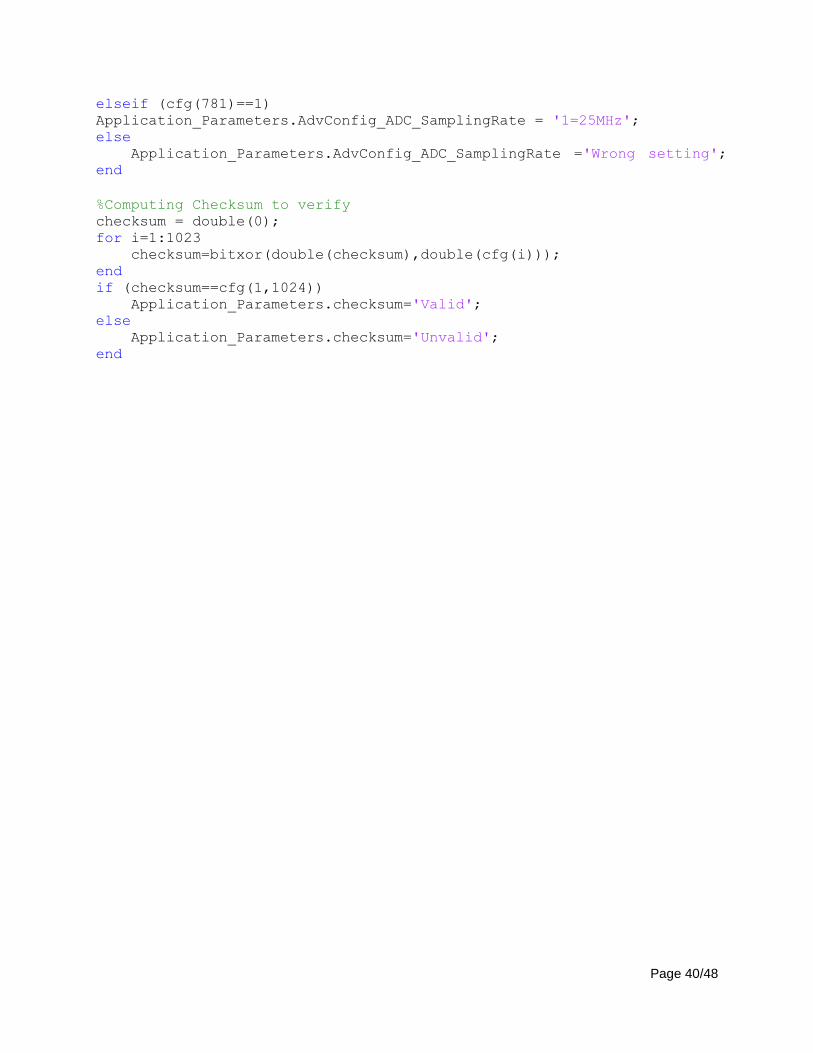
if (cfg(781)==0)
Application_Parameters.AdvConfig_ADC_SamplingRate = '0=100MHz';
Page 40/48
elseif (cfg(781)==1)
Application_Parameters.AdvConfig_ADC_SamplingRate = '1=25MHz';
else
Application_Parameters.AdvConfig_ADC_SamplingRate ='Wrong setting';
end
%Computing Checksum to verify
checksum = double(0);
for i=1:1023
checksum=bitxor(double(checksum),double(cfg(i)));
end
if (checksum==cfg(1,1024))
Application_Parameters.checksum='Valid';
else
Application_Parameters.checksum='Unvalid';
end
Page 41/48
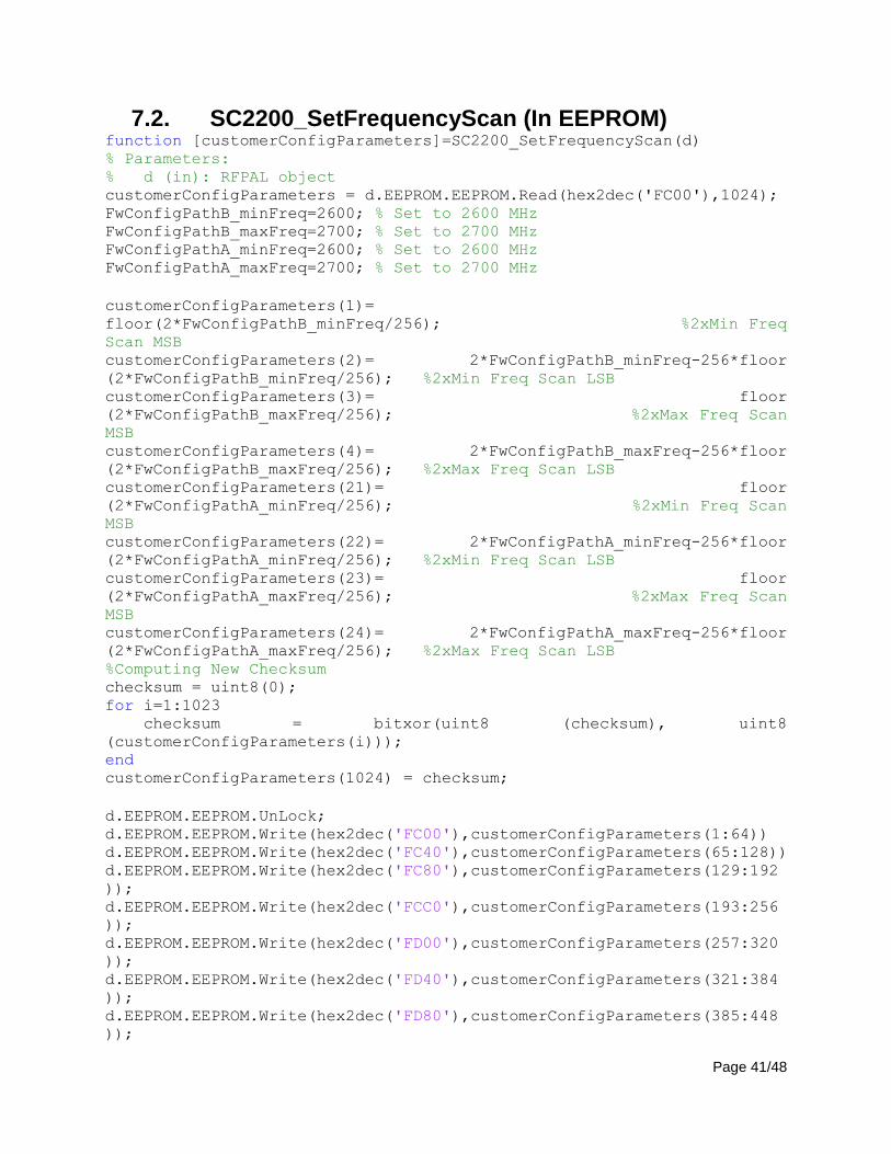
7.2. SC2200_SetFrequencyScan (In EEPROM) function [customerConfigParameters]=SC2200_SetFrequencyScan(d)
% Parameters:
% d (in): RFPAL object
customerConfigParameters = d.EEPROM.EEPROM.Read(hex2dec('FC00'),1024);
FwConfigPathB_minFreq=2600; % Set to 2600 MHz
FwConfigPathB_maxFreq=2700; % Set to 2700 MHz
FwConfigPathA_minFreq=2600; % Set to 2600 MHz
FwConfigPathA_maxFreq=2700; % Set to 2700 MHz
customerConfigParameters(1)=
floor(2*FwConfigPathB_minFreq/256); %2xMin Freq
Scan MSB
customerConfigParameters(2)= 2*FwConfigPathB_minFreq-256*floor
(2*FwConfigPathB_minFreq/256); %2xMin Freq Scan LSB
customerConfigParameters(3)= floor
(2*FwConfigPathB_maxFreq/256); %2xMax Freq Scan
MSB
customerConfigParameters(4)= 2*FwConfigPathB_maxFreq-256*floor
(2*FwConfigPathB_maxFreq/256); %2xMax Freq Scan LSB
customerConfigParameters(21)= floor
(2*FwConfigPathA_minFreq/256); %2xMin Freq Scan
MSB
customerConfigParameters(22)= 2*FwConfigPathA_minFreq-256*floor
(2*FwConfigPathA_minFreq/256); %2xMin Freq Scan LSB
customerConfigParameters(23)= floor
(2*FwConfigPathA_maxFreq/256); %2xMax Freq Scan
MSB
customerConfigParameters(24)= 2*FwConfigPathA_maxFreq-256*floor
(2*FwConfigPathA_maxFreq/256); %2xMax Freq Scan LSB
%Computing New Checksum
checksum = uint8(0);
for i=1:1023
checksum = bitxor(uint8 (checksum), uint8
(customerConfigParameters(i)));
end
customerConfigParameters(1024) = checksum;
d.EEPROM.EEPROM.UnLock;
d.EEPROM.EEPROM.Write(hex2dec('FC00'),customerConfigParameters(1:64))
d.EEPROM.EEPROM.Write(hex2dec('FC40'),customerConfigParameters(65:128))
d.EEPROM.EEPROM.Write(hex2dec('FC80'),customerConfigParameters(129:192
));
d.EEPROM.EEPROM.Write(hex2dec('FCC0'),customerConfigParameters(193:256
));
d.EEPROM.EEPROM.Write(hex2dec('FD00'),customerConfigParameters(257:320
));
d.EEPROM.EEPROM.Write(hex2dec('FD40'),customerConfigParameters(321:384
));
d.EEPROM.EEPROM.Write(hex2dec('FD80'),customerConfigParameters(385:448
));
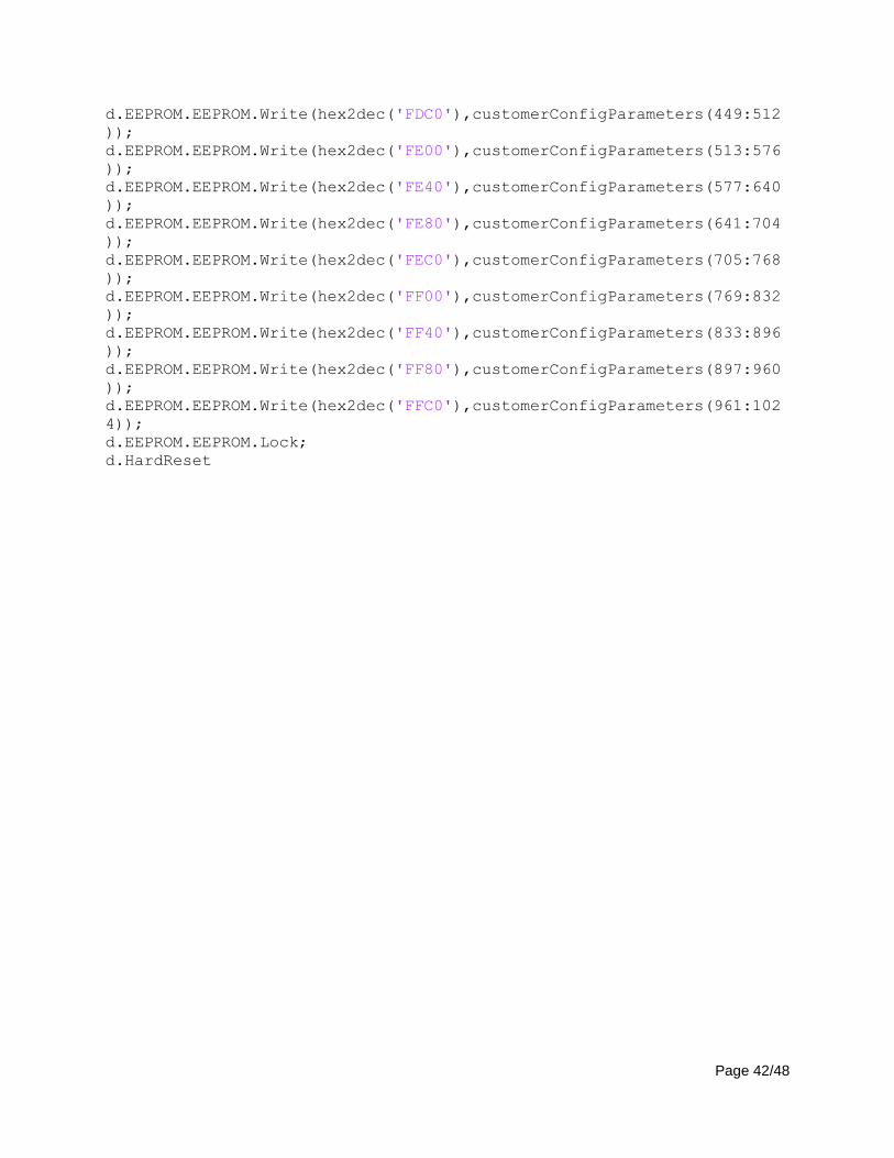
Page 42/48
d.EEPROM.EEPROM.Write(hex2dec('FDC0'),customerConfigParameters(449:512
));
d.EEPROM.EEPROM.Write(hex2dec('FE00'),customerConfigParameters(513:576
));
d.EEPROM.EEPROM.Write(hex2dec('FE40'),customerConfigParameters(577:640
));
d.EEPROM.EEPROM.Write(hex2dec('FE80'),customerConfigParameters(641:704
));
d.EEPROM.EEPROM.Write(hex2dec('FEC0'),customerConfigParameters(705:768
));
d.EEPROM.EEPROM.Write(hex2dec('FF00'),customerConfigParameters(769:832
));
d.EEPROM.EEPROM.Write(hex2dec('FF40'),customerConfigParameters(833:896
));
d.EEPROM.EEPROM.Write(hex2dec('FF80'),customerConfigParameters(897:960
));
d.EEPROM.EEPROM.Write(hex2dec('FFC0'),customerConfigParameters(961:102
4));
d.EEPROM.EEPROM.Lock;
d.HardReset
Page 43/48
7.3. SC2200_SetClockRef (In EEPROM) function [customerConfigParameters]=SC2200_SetClockRef(d, ClockRef)
% Parameters:
% d (in): RFPAL object
% ClockRef (in: Reference clock frequency in kHz
customerConfigParameters = d.EEPROM.EEPROM.Read(hex2dec('FC00'),1024);
customerConfigParameters(449)=
floor(ClockRef/256); %2xMin Freq Scan MSB
customerConfigParameters(450)= ClockRef-
256*floor(ClockRef/256); %2xMin Freq Scan LSB
%Computing New Checksum
checksum = uint8 (0);
for i=1:1023
checksum = bitxor(uint8 (checksum), uint8
(customerConfigParameters(i)));
end
%Compute the New Checksum: Modulo256 of all bytes added from FC00 to
FFFE
customerConfigParameters(1024) = checksum;
d.EEPROM.EEPROM.UnLock;
d.EEPROM.EEPROM.Write(hex2dec('FDC0'),customerConfigParameters(449:512
));
d.EEPROM.EEPROM.Write(hex2dec('FFC0'),customerConfigParameters(961:102
4));
d.EEPROM.EEPROM.Lock;
d.HardReset %Hardware or SoftReset
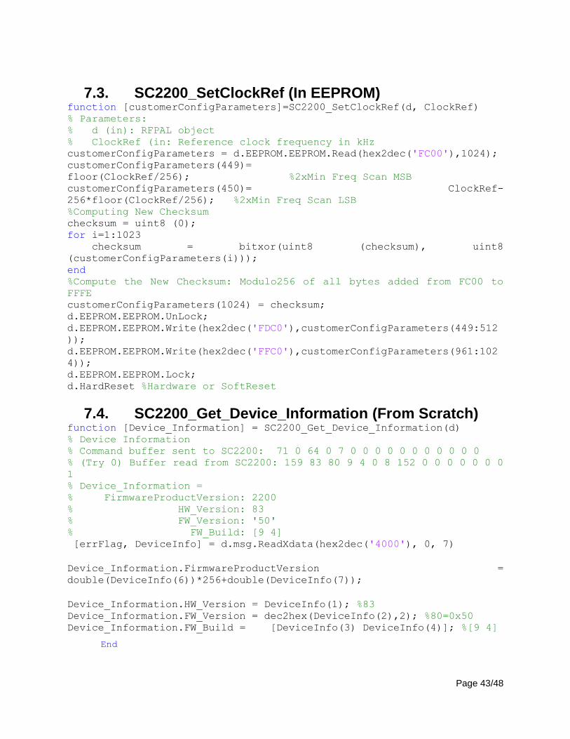
7.4. SC2200_Get_Device_Information (From Scratch) function [Device_Information] = SC2200_Get_Device_Information(d)
% Device Information
% Command buffer sent to SC2200: 71 0 64 0 7 0 0 0 0 0 0 0 0 0 0 0
% (Try 0) Buffer read from SC2200: 159 83 80 9 4 0 8 152 0 0 0 0 0 0 0
1
% Device_Information =
% FirmwareProductVersion: 2200
% HW_Version: 83
% FW_Version: '50'
% FW_Build: [9 4]
[errFlag, DeviceInfo] = d.msg.ReadXdata(hex2dec('4000'), 0, 7)
Device_Information.FirmwareProductVersion =
double(DeviceInfo(6))*256+double(DeviceInfo(7));
Device_Information.HW_Version = DeviceInfo(1); %83
Device_Information.FW_Version = dec2hex(DeviceInfo(2),2); %80=0x50
Device_Information.FW_Build = [DeviceInfo(3) DeviceInfo(4)]; %[9 4]
End
Page 44/48
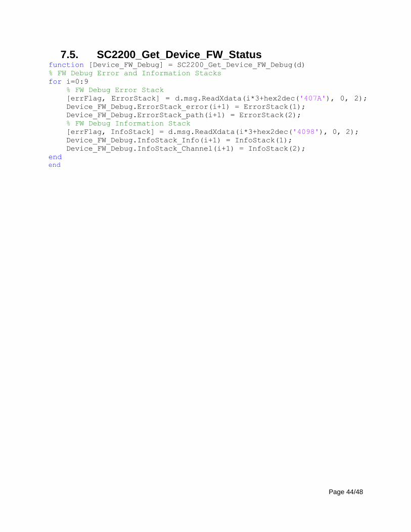
7.5. SC2200_Get_Device_FW_Status function [Device_FW_Debug] = SC2200_Get_Device_FW_Debug(d)
% FW Debug Error and Information Stacks
for i=0:9
% FW Debug Error Stack
[errFlag, ErrorStack] = d.msg.ReadXdata(i*3+hex2dec('407A'), 0, 2);
Device_FW_Debug.ErrorStack_error(i+1) = ErrorStack(1);
Device_FW_Debug.ErrorStack_path(i+1) = ErrorStack(2);
% FW Debug Information Stack
[errFlag, InfoStack] = d.msg.ReadXdata(i*3+hex2dec('4098'), 0, 2);
Device_FW_Debug.InfoStack_Info(i+1) = InfoStack(1);
Device_FW_Debug.InfoStack_Channel(i+1) = InfoStack(2);
end end
Page 45/48
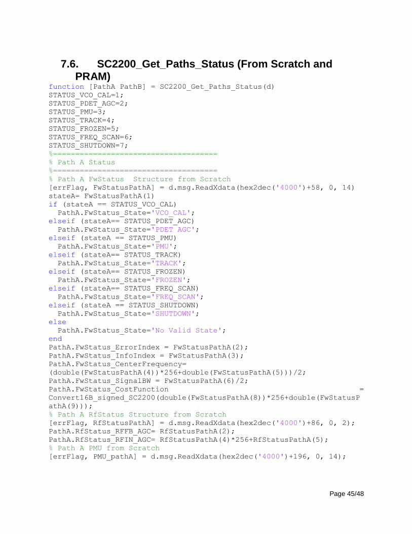
7.6. SC2200_Get_Paths_Status (From Scratch and PRAM)
function [PathA PathB] = SC2200_Get_Paths_Status(d)
STATUS_VCO_CAL=1;
STATUS_PDET_AGC=2;
STATUS_PMU=3;
STATUS_TRACK=4;
STATUS_FROZEN=5;
STATUS_FREQ_SCAN=6;
STATUS_SHUTDOWN=7;
%=====================================
% Path A Status
%=====================================
% Path A FwStatus Structure from Scratch
[errFlag, FwStatusPathA] = d.msg.ReadXdata(hex2dec('4000')+58, 0, 14)
stateA= FwStatusPathA(1)
if (stateA == STATUS_VCO_CAL)
PathA.FwStatus_State='VCO_CAL';
elseif (stateA== STATUS_PDET_AGC)
PathA.FwStatus_State='PDET AGC';
elseif (stateA == STATUS_PMU)
PathA.FwStatus_State='PMU';
elseif (stateA== STATUS_TRACK)
PathA.FwStatus_State='TRACK';
elseif (stateA== STATUS_FROZEN)
PathA.FwStatus_State='FROZEN';
elseif (stateA== STATUS_FREQ_SCAN)
PathA.FwStatus_State='FREQ_SCAN';
elseif (stateA == STATUS_SHUTDOWN)
PathA.FwStatus_State='SHUTDOWN';
else
PathA.FwStatus_State='No Valid State';
end
PathA.FwStatus_ErrorIndex = FwStatusPathA(2);
PathA.FwStatus_InfoIndex = FwStatusPathA(3);
PathA.FwStatus_CenterFrequency=
(double(FwStatusPathA(4))*256+double(FwStatusPathA(5)))/2;
PathA.FwStatus_SignalBW = FwStatusPathA(6)/2;
PathA.FwStatus_CostFunction =
Convert16B_signed_SC2200(double(FwStatusPathA(8))*256+double(FwStatusP
athA(9)));
% Path A RfStatus Structure from Scratch
[errFlag, RfStatusPathA] = d.msg.ReadXdata(hex2dec('4000')+86, 0, 2);
PathA.RfStatus_RFFB_AGC= RfStatusPathA(2);
PathA.RfStatus_RFIN_AGC= RfStatusPathA(4)*256+RfStatusPathA(5);
% Path A PMU from Scratch
[errFlag, PMU_pathA] = d.msg.ReadXdata(hex2dec('4000')+196, 0, 14);
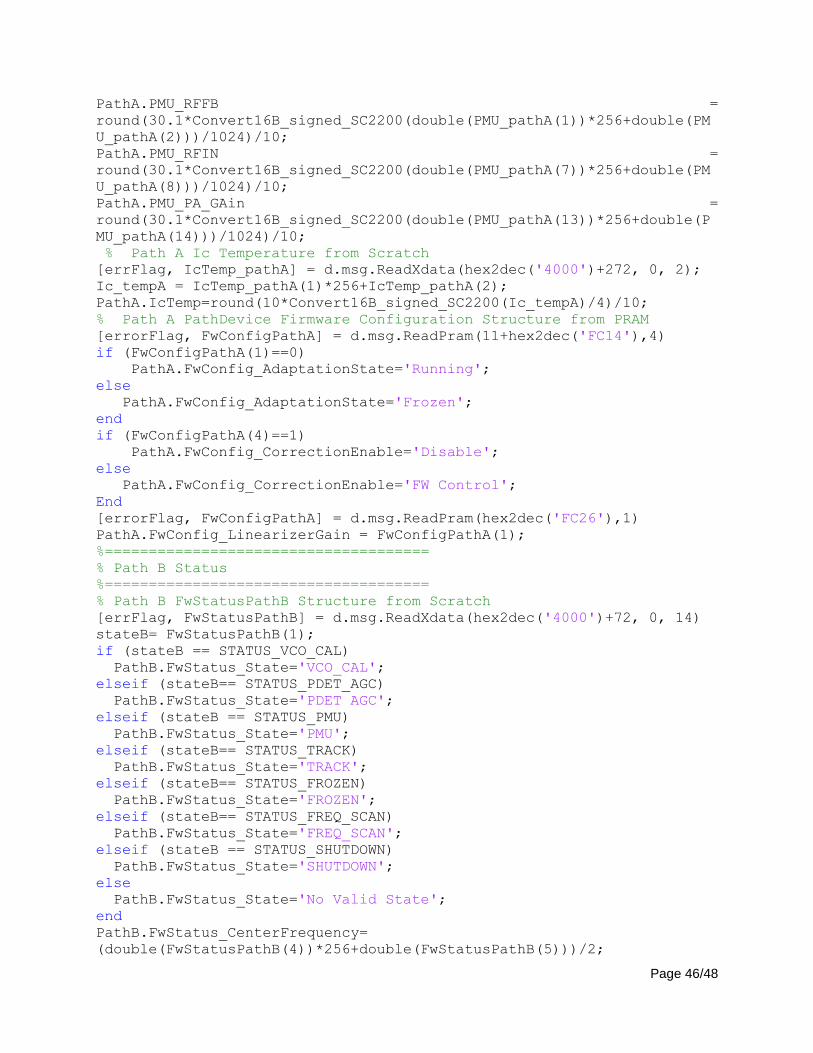
Page 46/48
PathA.PMU_RFFB =
round(30.1*Convert16B_signed_SC2200(double(PMU_pathA(1))*256+double(PM
U_pathA(2)))/1024)/10;
PathA.PMU_RFIN =
round(30.1*Convert16B_signed_SC2200(double(PMU_pathA(7))*256+double(PM
U_pathA(8)))/1024)/10;
PathA.PMU_PA_GAin =
round(30.1*Convert16B_signed_SC2200(double(PMU_pathA(13))*256+double(P
MU_pathA(14)))/1024)/10;
% Path A Ic Temperature from Scratch
[errFlag, IcTemp_pathA] = d.msg.ReadXdata(hex2dec('4000')+272, 0, 2);
Ic_tempA = IcTemp_pathA(1)*256+IcTemp_pathA(2);
PathA.IcTemp=round(10*Convert16B_signed_SC2200(Ic_tempA)/4)/10;
% Path A PathDevice Firmware Configuration Structure from PRAM
[errorFlag, FwConfigPathA] = d.msg.ReadPram(11+hex2dec('FC14'),4)
if (FwConfigPathA(1)==0)
PathA.FwConfig_AdaptationState='Running';
else
PathA.FwConfig_AdaptationState='Frozen';
end
if (FwConfigPathA(4)==1)
PathA.FwConfig_CorrectionEnable='Disable';
else
PathA.FwConfig_CorrectionEnable='FW Control';
End
[errorFlag, FwConfigPathA] = d.msg.ReadPram(hex2dec('FC26'),1)
PathA.FwConfig_LinearizerGain = FwConfigPathA(1);
%=====================================
% Path B Status
%=====================================
% Path B FwStatusPathB Structure from Scratch
[errFlag, FwStatusPathB] = d.msg.ReadXdata(hex2dec('4000')+72, 0, 14)
stateB= FwStatusPathB(1);
if (stateB == STATUS_VCO_CAL)
PathB.FwStatus_State='VCO_CAL';
elseif (stateB== STATUS_PDET_AGC)
PathB.FwStatus_State='PDET AGC';
elseif (stateB == STATUS_PMU)
PathB.FwStatus_State='PMU';
elseif (stateB== STATUS_TRACK)
PathB.FwStatus_State='TRACK';
elseif (stateB== STATUS_FROZEN)
PathB.FwStatus_State='FROZEN';
elseif (stateB== STATUS_FREQ_SCAN)
PathB.FwStatus_State='FREQ_SCAN';
elseif (stateB == STATUS_SHUTDOWN)
PathB.FwStatus_State='SHUTDOWN';
else
PathB.FwStatus_State='No Valid State';
end
PathB.FwStatus_CenterFrequency=
(double(FwStatusPathB(4))*256+double(FwStatusPathB(5)))/2;
Page 47/48
PathB.FwStatus_SignalBW = FwStatusPathB(6)/2;
PathB.FwStatus_CostFunction =
Convert16B_signed_SC2200(double(FwStatusPathB(8))*256+double(FwStatusP
athB(9)));
% Path BRfStatus Structure from Scratch
[errFlag, RfStatusPathB] = d.msg.ReadXdata(hex2dec('4000')+104, 0, 2);
PathB.RfStatus_RFFB_AGC= RfStatusPathB(2);
PathB.RfStatus_RFIN_AGC= RfStatusPathB(4)*256+RfStatusPathB(5);
% Path B PMU from Scratch
[errFlag, PMU_pathB] = d.msg.ReadXdata(hex2dec('4000')+182, 0, 14);
PathB.PMU_RFFB =
round(30.1*Convert16B_signed_SC2200(double(PMU_pathB(1))*256+double(PM
U_pathB(2)))/1024)/10;
PathB.PMU_RFIN =
round(30.1*Convert16B_signed_SC2200(double(PMU_pathB(7))*256+double(PM
U_pathB(8)))/1024)/10;
PathB.PMU_PA_GAin =
round(30.1*Convert16B_signed_SC2200(double(PMU_pathB(13))*256+double(P
MU_pathB(14)))/1024)/10;
% Path B IcTemp from Scratch
[errFlag, IcTemp_pathB] = d.msg.ReadXdata(hex2dec('4000')+374, 0, 2);
Ic_tempB = IcTemp_pathB(1)*256+IcTemp_pathB(2);
PathB.IcTemp=round(10*Convert16B_signed_SC2200(Ic_tempB)/4)/10;
% Path B PathDevice Firmware Configuration Structure from PRAM
[errorFlag, FwConfigPathB] = d.msg.ReadPram(11+hex2dec('FC00'),4)
if (FwConfigPathB(1)==0)
PathB.FwConfig_AdaptationState='Running';
else
PathB.FwConfig_AdaptationState='Frozen';
end
if (FwConfigPathB(4)==1)
PathB.FwConfig_CorrectionEnable='Disable';
else
PathB.FwConfig_CorrectionEnable='FW Control';
end
[errorFlag, FwConfigPathB] = d.msg.ReadPram(hex2dec('FC12'),1)
PathB.FwConfig_LinearizerGain = FwConfigPathB(1);
7.7. SC2200_Clear_Calibration Please refer to section 6 for the 16-byte host command for clear
Calibration.
function [errorFlag] = SC2200_Clear_Calibration( d, Path) % d: SC2200 handler. Path: Path A=0 Path B = 1 if(nargin < 2) Path = 0; end errorFlag = d.msg.ClearCalibrationData(Path, 0);
Page 48/48
7.8. SC2200_Set_Cal ibration Please refer to section 6.2 for the 16-byte host command for Set Calibration. function [errorFlag] = SC2200_Set_Calibration( d, Path) % d: SC2200 handler. Path: Path A=0 Path B = 1 if(nargin < 2) Path = 0; end errorFlag = d.msg.SetCalibrationData(Path, 0); end
7.9. Clear InfoStack function [errFlag] = SC2200_Clear_InfoStack(d)
%Write 1 to Global Scratch address 0x330
errFlag = d.msg.WriteXdata(hex2dec('4330'),0,1);
7.10. Convert16B_Signed SC2200 (PRAM, Scratch and EEPROM)
function [Signed_16Bits_value]= Convert16B_signed_SC2200(value)
%Scratch is big Endian
if (value>hex2dec('7FFF')) % Negative value
Signed_16Bits_value=double(value)-65536;
else % Positive value
Signed_16Bits_value=double(value);
end
©2016 by Maxim Integrated Products, Inc. All rights reserved. Information in this publication concerning the devices,
applications, or technology described is intended to suggest possible uses and may be superseded. MAXIM
INTEGRATED PRODUCTS, INC. DOES NOT ASSUME LIABILITY FOR OR PROVIDE A REPRESENTATION OF
ACCURACY OF THE INFORMATION, DEVICES, OR TECHNOLOGY DESCRIBED IN THIS DOCUMENT. MAXIM
ALSO DOES NOT ASSUME LIABILITY FOR INTELLECTUAL PROPERTY INFRINGEMENT RELATED IN ANY
MANNER TO USE OF INFORMATION, DEVICES, OR TECHNOLOGY DESCRIBED HEREIN OR OTHERWISE.
The information contained within this document has been verified according to the general principles of electrical and
mechanical engineering or registered trademarks of Maxim Integrated Products, Inc. All other product or service
names are the property of their respective owners.