Embed Size (px)
Citation preview
SBVS012E − DECEMBER 2000 − REVISED DECEMBER 2007
!"#
FEATURES Up To 85% Efficiency
Thermal Protection
Device-to-Device Synchronization
Short-Circuit Protection
EN55022 Class B EMC Performance
UL1950 Recognized Component
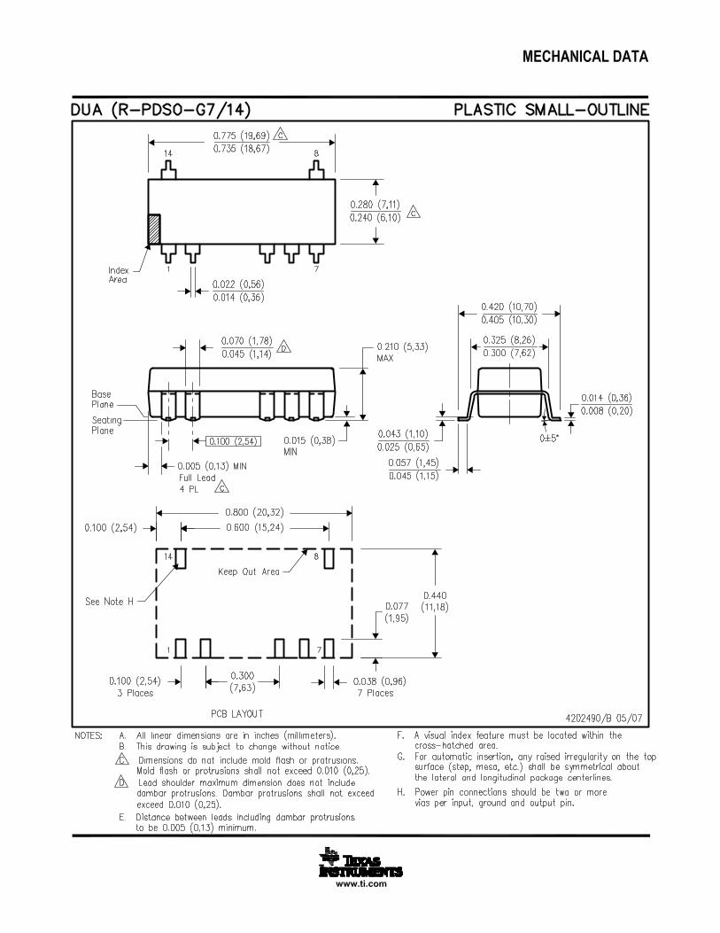
JEDEC DIP-14 and SOP-14 Packages
APPLICATIONS Point-of-Use Power Conversion
Ground Loop Elimination
Data Acquisition
Industrial Control and Instrumentation
Test Equipment
DESCRIPTION
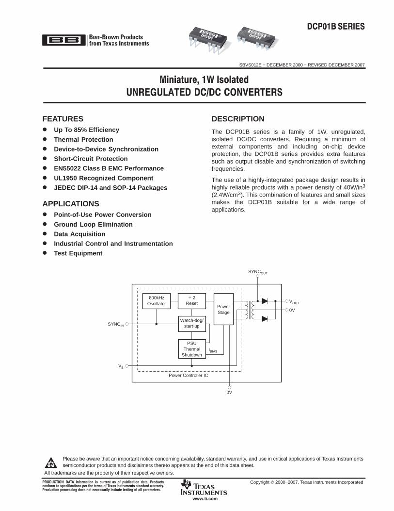
The DCP01B series is a family of 1W, unregulated,isolated DC/DC converters. Requiring a minimum ofexternal components and including on-chip deviceprotection, the DCP01B series provides extra featuressuch as output disable and synchronization of switchingfrequencies.
The use of a highly-integrated package design results inhighly reliable products with a power density of 40W/in3
(2.4W/cm3). This combination of features and small sizesmakes the DCP01B suitable for a wide range ofapplications.
IBIAS
PowerStage
VOUT
÷ 2Reset
800kHzOscillator
Watch−dog/start−up
PSUThermal
Shutdown
SYNCOUT
SYNCIN
VS
0V
Power Controller IC
0V
www.ti.com
Copyright 2000−2007, Texas Instruments Incorporated
Please be aware that an important notice concerning availability, standard warranty, and use in critical applications of Texas Instrumentssemiconductor products and disclaimers thereto appears at the end of this data sheet.
All trademarks are the property of their respective owners.
! $% & $ '(& ) !&&$% '&$& ' * % $ + % ,-)!& '&. &- & . $ '%)
!"#
SBVS012E − DECEMBER 2000 − REVISED DECEMBER 2007
www.ti.com
2
This integrated circuit can be damaged by ESD. Texas Instruments recommends that all integrated circuits be handled with appropriateprecautions. Failure to observe proper handling and installation procedures can cause damage.
ESD damage can range from subtle performance degradation to complete device failure. Precision integrated circuits may be more susceptible todamage because very small parametric changes could cause the device not to meet its published specifications.
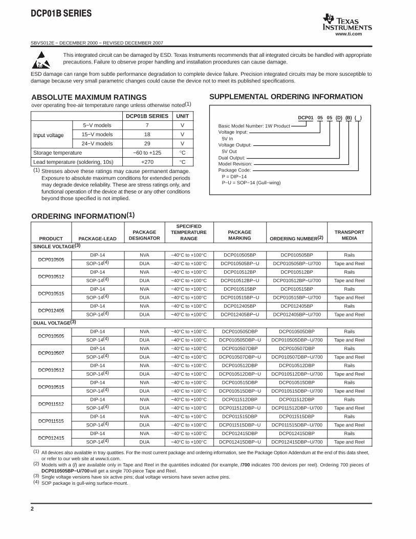
ABSOLUTE MAXIMUM RATINGSover operating free-air temperature range unless otherwise noted(1)
DCP01B SERIES UNIT
5−V models 7 V
Input voltage 15−V models 18 VInput voltage
24−V models 29 V
Storage temperature −60 to +125 °C
Lead temperature (soldering, 10s) +270 °C(1) Stresses above these ratings may cause permanent damage.
Exposure to absolute maximum conditions for extended periodsmay degrade device reliability. These are stress ratings only, andfunctional operation of the device at these or any other conditionsbeyond those specified is not implied.
SUPPLEMENTAL ORDERING INFORMATION
Basic Model Number: 1W ProductVoltage Input:
5V InVoltage Output:
Dual Output:Model Revision:Package Code:
5V Out
P = DIP−14P−U = SOP−14 (Gull−wing)
DCP01 05 05 (D) (B) ( )
ORDERING INFORMATION(1)
PRODUCT PACKAGE-LEADPACKAGE
DESIGNATOR
SPECIFIEDTEMPERATURE
RANGEPACKAGEMARKING ORDERING NUMBER(2)
TRANSPORTMEDIA
SINGLE VOLTAGE(3)
DCP010505DIP-14 NVA −40°C to +100°C DCP010505BP DCP010505BP Rails
DCP010505SOP-14(4) DUA −40°C to +100°C DCP010505BP−U DCP010505BP−U/700 Tape and Reel
DCP010512DIP-14 NVA −40°C to +100°C DCP010512BP DCP010512BP Rails
DCP010512SOP-14(4) DUA −40°C to +100°C DCP010512BP−U DCP010512BP−U/700 Tape and Reel
DCP010515DIP-14 NVA −40°C to +100°C DCP010515BP DCP010515BP Rails
DCP010515SOP-14(4) DUA −40°C to +100°C DCP010515BP−U DCP010515BP−U/700 Tape and Reel
DCP012405DIP-14 NVA −40°C to +100°C DCP012405BP DCP012405BP Rails
DCP012405SOP-14(4) DUA −40°C to +100°C DCP012405BP−U DCP012405BP−U/700 Tape and Reel
DUAL VOLTAGE(3)
DCP010505DIP-14 NVA −40°C to +100°C DCP010505DBP DCP010505DBP Rails
DCP010505SOP-14(4) DUA −40°C to +100°C DCP010505DBP−U DCP010505DBP−U/700 Tape and Reel
DCP010507DIP-14 NVA −40°C to +100°C DCP010507DBP DCP010507DBP Rails
DCP010507SOP-14(4) DUA −40°C to +100°C DCP010507DBP−U DCP010507DBP−U/700 Tape and Reel
DCP010512DIP-14 NVA −40°C to +100°C DCP010512DBP DCP010512DBP Rails
DCP010512SOP-14(4) DUA −40°C to +100°C DCP010512DBP−U DCP010512DBP−U/700 Tape and Reel
DCP010515DIP-14 NVA −40°C to +100°C DCP010515DBP DCP010515DBP Rails
DCP010515SOP-14(4) DUA −40°C to +100°C DCP010515DBP−U DCP010515DBP−U/700 Tape and Reel
DCP011512DIP-14 NVA −40°C to +100°C DCP011512DBP DCP011512DBP Rails
DCP011512SOP-14(4) DUA −40°C to +100°C DCP011512DBP−U DCP011512DBP−U/700 Tape and Reel
DCP011515DIP-14 NVA −40°C to +100°C DCP011515DBP DCP011515DBP Rails
DCP011515SOP-14(4) DUA −40°C to +100°C DCP011515DBP−U DCP011515DBP−U/700 Tape and Reel
DCP012415DIP-14 NVA −40°C to +100°C DCP012415DBP DCP012415DBP Rails
DCP012415SOP-14(4) DUA −40°C to +100°C DCP012415DBP−U DCP012415DBP−U/700 Tape and Reel
(1) All devices also available in tray quatities. For the most current package and ordering information, see the Package Option Addendum at the end of this data sheet,or refer to our web site at www.ti.com.
(2) Models with a (/) are available only in Tape and Reel in the quantities indicated (for example, /700 indicates 700 devices per reel). Ordering 700 pieces ofDCP010505BP−U/700 will get a single 700-piece Tape and Reel.
(3) Single voltage versions have six active pins; dual voltage versions have seven active pins.(4) SOP package is gull-wing surface-mount.
!"#
SBVS012E − DECEMBER 2000 − REVISED DECEMBER 2007
www.ti.com
3
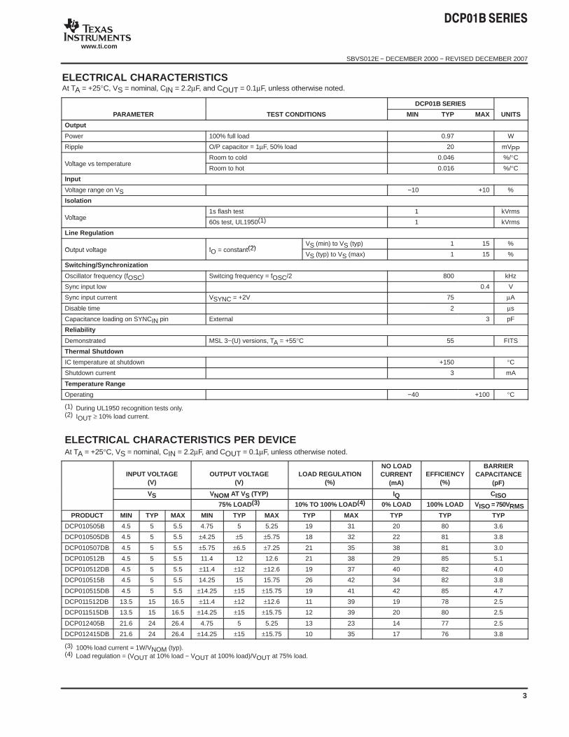
ELECTRICAL CHARACTERISTICS At TA = +25°C, VS = nominal, CIN = 2.2µF, and COUT = 0.1µF, unless otherwise noted.
DCP01B SERIES
PARAMETER TEST CONDITIONS MIN TYP MAX UNITS
Output
Power 100% full load 0.97 W
Ripple O/P capacitor = 1µF, 50% load 20 mVPP
Voltage vs temperatureRoom to cold 0.046 %/°C
Voltage vs temperatureRoom to hot 0.016 %/°C
Input
Voltage range on VS −10 +10 %
Isolation
Voltage1s flash test 1 kVrms
Voltage60s test, UL1950(1) 1 kVrms
Line Regulation
Output voltage IO = constant(2)VS (min) to VS (typ) 1 15 %
Output voltage IO = constant(2)VS (typ) to VS (max) 1 15 %
Switching/Synchronization
Oscillator frequency (fOSC) Switcing frequency = fOSC/2 800 kHz
Sync input low 0.4 V
Sync input current VSYNC = +2V 75 µA
Disable time 2 µs
Capacitance loading on SYNCIN pin External 3 pF
Reliability
Demonstrated MSL 3−(U) versions, TA = +55°C 55 FITS
Thermal Shutdown
IC temperature at shutdown +150 °C
Shutdown current 3 mA
Temperature Range
Operating −40 +100 °C
(1) During UL1950 recognition tests only.(2) IOUT ≥ 10% load current.
ELECTRICAL CHARACTERISTICS PER DEVICEAt TA = +25°C, VS = nominal, CIN = 2.2µF, and COUT = 0.1µF, unless otherwise noted.
INPUT VOLTAGE(V)
OUTPUT VOLTAGE(V)
LOAD REGULATION(%)
NO LOADCURRENT
(mA)EFFICIENCY
(%)
BARRIERCAPACITANCE
(pF)
VS VNOM AT VS (TYP) IQ CISO75% LOAD(3) 10% TO 100% LOAD(4) 0% LOAD 100% LOAD VISO = 750VRMS
PRODUCT MIN TYP MAX MIN TYP MAX TYP MAX TYP TYP TYP
DCP010505B 4.5 5 5.5 4.75 5 5.25 19 31 20 80 3.6
DCP010505DB 4.5 5 5.5 ±4.25 ±5 ±5.75 18 32 22 81 3.8
DCP010507DB 4.5 5 5.5 ±5.75 ±6.5 ±7.25 21 35 38 81 3.0
DCP010512B 4.5 5 5.5 11.4 12 12.6 21 38 29 85 5.1
DCP010512DB 4.5 5 5.5 ±11.4 ±12 ±12.6 19 37 40 82 4.0
DCP010515B 4.5 5 5.5 14.25 15 15.75 26 42 34 82 3.8
DCP010515DB 4.5 5 5.5 ±14.25 ±15 ±15.75 19 41 42 85 4.7
DCP011512DB 13.5 15 16.5 ±11.4 ±12 ±12.6 11 39 19 78 2.5
DCP011515DB 13.5 15 16.5 ±14.25 ±15 ±15.75 12 39 20 80 2.5
DCP012405B 21.6 24 26.4 4.75 5 5.25 13 23 14 77 2.5
DCP012415DB 21.6 24 26.4 ±14.25 ±15 ±15.75 10 35 17 76 3.8
(3) 100% load current = 1W/VNOM (typ).(4) Load regulation = (VOUT at 10% load − VOUT at 100% load)/VOUT at 75% load.
!"#
SBVS012E − DECEMBER 2000 − REVISED DECEMBER 2007
www.ti.com
4
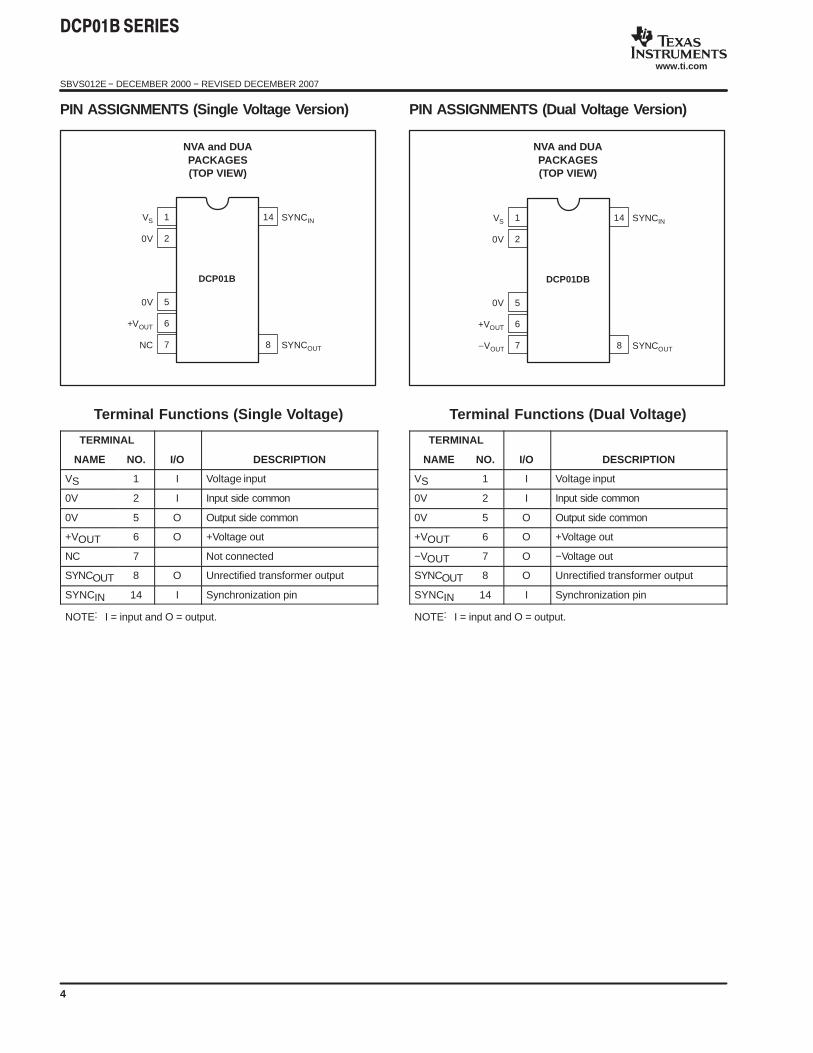
PIN ASSIGNMENTS (Single Voltage Version)
NVA and DUAPACKAGES(TOP VIEW)
DCP01B
1
2
5
6
7
14
8
VS
0V
0V
+VOUT
NC
SYNCIN
SYNCOUT
Terminal Functions (Single Voltage)
TERMINAL
NAME NO. I/O DESCRIPTION
VS 1 I Voltage input
0V 2 I Input side common
0V 5 O Output side common
+VOUT 6 O +Voltage out
NC 7 Not connected
SYNCOUT 8 O Unrectified transformer output
SYNCIN 14 I Synchronization pin
NOTE: I = input and O = output.
PIN ASSIGNMENTS (Dual Voltage Version)
NVA and DUAPACKAGES(TOP VIEW)
DCP01DB
1
2
5
6
7
14
8
VS
0V
0V
+VOUT
−VOUT
SYNCIN
SYNCOUT
Terminal Functions (Dual Voltage)
TERMINAL
NAME NO. I/O DESCRIPTION
VS 1 I Voltage input
0V 2 I Input side common
0V 5 O Output side common
+VOUT 6 O +Voltage out
−VOUT 7 O −Voltage out
SYNCOUT 8 O Unrectified transformer output
SYNCIN 14 I Synchronization pin
NOTE: I = input and O = output.
!"#
SBVS012E − DECEMBER 2000 − REVISED DECEMBER 2007
www.ti.com
5
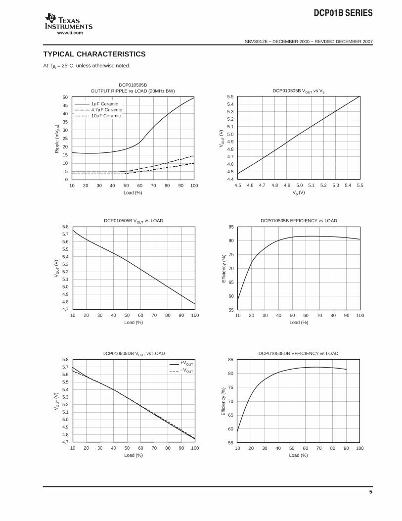
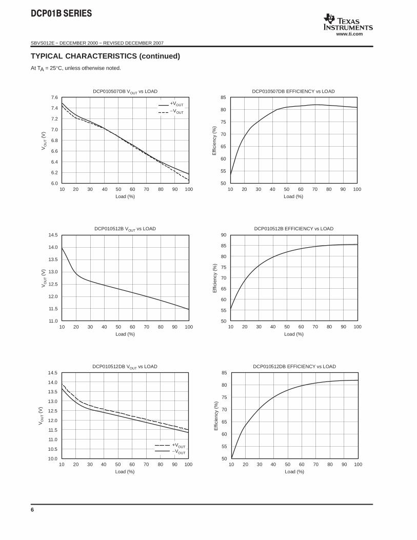
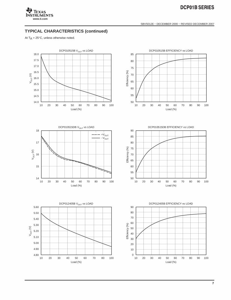
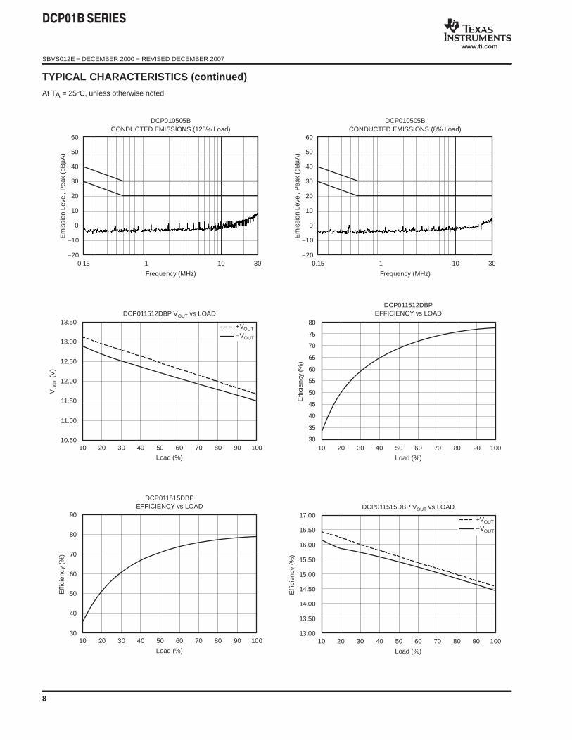
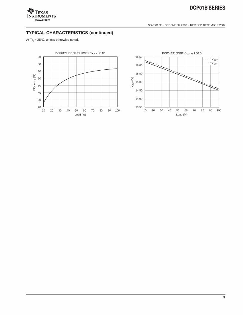
TYPICAL CHARACTERISTICS
At TA = 25°C, unless otherwise noted.
DCP010505BOUTPUT RIPPLE vs LOAD (20MHz BW)
Load (%)
Rip
ple
(mV
PP)
50
45
40
35
30
25
20
15
10
5
020 30 50 7060 80 90 1004010
1µF Ceramic4.7µF Ceramic10µF Ceramic
DCP010505B VOUT vs VS
VS (V)
VO
UT
(V)
5.5
5.4
5.3
5.2
5.1
5.0
4.9
4.8
4.7
4.6
4.5
4.44.6 4.7 4.9 5.15.0 5.2 5.45.3 5.54.84.5
DCP010505B VOUT vs LOAD
Load (%)
VO
UT
(V)
5.8
5.7
5.6
5.5
5.4
5.3
5.2
5.1
5.0
4.9
4.8
4.710010 20 30 40 50 60 70 80 90
DCP010505B EFFICIENCY vs LOAD
Load (%)
Effi
cie
ncy
(%)
85
80
75
70
65
60
5510010 20 30 40 50 60 70 80 90
DCP010505DB VOUT vs LOAD
Load (%)
VO
UT
(V)
5.8
5.7
5.6
5.5
5.4
5.3
5.2
5.1
5.0
4.9
4.8
4.710010 20 30 40 50 60 70 80 90
+VOUT
−VOUT
DCP010505DB EFFICIENCY vs LOAD
Load (%)
Effi
cie
ncy
(%)
85
80
75
70
65
60
5510010 20 30 40 50 60 70 80 90
!"#
SBVS012E − DECEMBER 2000 − REVISED DECEMBER 2007
www.ti.com
6
TYPICAL CHARACTERISTICS (continued)
At TA = 25°C, unless otherwise noted.
DCP010507DB VOUT vs LOAD
Load (%)
VO
UT
(V)
7.6
7.4
7.2
7.0
6.8
6.6
6.4
6.2
6.010010 20 30 40 50 60 70 80 90
+VOUT
−VOUT
DCP010507DB EFFICIENCY vs LOAD
Load (%)
Effi
cien
cy(%
)
85
80
75
70
65
60
55
5010010 20 30 40 50 60 70 80 90
DCP010512B VOUT vs LOAD
Load (%)
VO
UT
(V)
14.5
14.0
13.5
13.0
12.5
12.0
11.5
11.010010 20 30 40 50 60 70 80 90
DCP010512B EFFICIENCY vs LOAD
Load (%)
Effi
cien
cy(%
)
90
85
80
75
70
65
60
55
5010010 20 30 40 50 60 70 80 90
DCP010512DB VOUT vs LOAD
Load (%)
VO
UT
(V)
14.5
14.0
13.5
13.0
12.5
12.0
11.5
11.0
10.5
10.020 30 50 7060 80 90 1004010
+VOUT−VOUT
DCP010512DB EFFICIENCY vs LOAD
Load (%)
Effi
cie
ncy
(%)
85
80
75
70
65
60
55
5020 30 50 7060 80 90 1004010
!"#
SBVS012E − DECEMBER 2000 − REVISED DECEMBER 2007
www.ti.com
7
TYPICAL CHARACTERISTICS (continued)
At TA = 25°C, unless otherwise noted.
DCP010515B VOUT vs LOAD
Load (%)
VO
UT
(V)
18.0
17.5
17.0
16.5
16.0
15.5
15.0
14.5
14.010010 20 30 40 50 60 70 80 90
DCP010515B EFFICIENCY vs LOAD
Load (%)
Effi
cien
cy(%
)
85
80
75
70
65
60
55
5010010 20 30 40 50 60 70 80 90
DCP010515DB VOUT vs LOAD
Load (%)
VO
UT
(V)
18
17
16
15
1420 30 50 7060 80 90 1004010
+VOUT−VOUT
DCP010515DB EFFICIENCY vs LOAD
Load (%)
Effi
cie
ncy
(%)
90
85
80
75
70
65
60
55
5020 30 50 7060 80 90 1004010
DCP012405B VOUT vs LOAD
Load (%)
VO
UT
(V)
5.60
5.50
5.40
5.30
5.20
5.10
5.00
4.90
4.8020 30 6050 70 80 1004010
DCP012405B EFFICIENCY vs LOAD
Load (%)
Effi
cie
ncy
(%)
90
80
70
60
50
40
30
20
10
020 30 7060 80 90 10040 5010
!"#
SBVS012E − DECEMBER 2000 − REVISED DECEMBER 2007
www.ti.com
8
TYPICAL CHARACTERISTICS (continued)
At TA = 25°C, unless otherwise noted.
DCP010505BCONDUCTED EMISSIONS (125% Load)
Em
issi
onL
evel
,P
eak
(dB
µ A)
Frequency (MHz)
10.15 10 30
60
50
40
30
20
10
0
−10
−20
DCP010505BCONDUCTED EMISSIONS (8% Load)
Em
issi
onL
evel
,P
eak
(dB
µ A)
Frequency (MHz)
10.15 10 30
60
50
40
30
20
10
0
−10
−20
DCP011512DBP VOUT vs LOAD
Load (%)
VO
UT
(V)
13.50
13.00
12.50
12.00
11.50
11.00
10.5010010 20 30 40 50 60 70 80 90
+VOUT
−VOUT
DCP011512DBPEFFICIENCY vs LOAD
Load (%)
Effi
cie
ncy
(%)
80
75
70
65
60
55
50
45
40
35
3020 30 50 7060 80 90 1004010
DCP011515DBPEFFICIENCY vs LOAD
Load (%)
Effi
cie
ncy
(%)
90
80
70
60
50
40
3010010 20 30 40 50 60 70 80 90
DCP011515DBP VOUT vs LOAD
Load (%)
Effi
cien
cy(%
)
17.00
16.50
16.00
15.50
15.00
14.50
14.00
13.50
13.0010010 20 30 40 50 60 70 80 90
+VOUT
−VOUT
!"#
SBVS012E − DECEMBER 2000 − REVISED DECEMBER 2007
www.ti.com
9
TYPICAL CHARACTERISTICS (continued)
At TA = 25°C, unless otherwise noted.
DCP012415DBP EFFICIENCY vs LOAD
Load (%)
Effi
cien
cy(%
)
90
80
70
60
50
40
30
2010010 20 30 40 50 60 70 80 90
DCP012415DBP VOUT vs LOAD
Load (%)
VO
UT
(V)
16.50
16.00
15.50
15.00
14.50
14.00
13.5010010 20 30 40 50 60 70 80 90
+VOUT−VOUT
!"#
SBVS012E − DECEMBER 2000 − REVISED DECEMBER 2007
www.ti.com
10
FUNCTIONAL DESCRIPTION
OVERVIEW
The DCP01B offers up to 1W of unregulated output powerwith a typical efficiency of up to 85%. This is achievedthrough highly integrated packaging technology and theimplementation of a custom power stage and control IC.The circuit design uses an advanced BiCMOS/DMOSprocess. For additional information, refer to the applicationnotes located in the DCP01B product folder at www.ti.com.
POWER STAGE
This uses a push-pull, center-tapped topology switching at400kHz (divide-by-2 from 800kHz oscillator).
OSCILLATOR AND WATCHDOG
The onboard 800kHz oscillator generates the switchingfrequency via a divide-by-2 circuit. The oscillator can besynchronized to other DCP01B circuits or an externalsource, and is used to minimize system noise.
A watchdog circuit checks the operation of the oscillatorcircuit. The oscillator can be stopped by pulling the SYNCpin low. The output pins will be tri-stated. This will occur in2µs.
THERMAL SHUTDOWN
The DCP01B is protected by a thermal shutdown circuit.If the on-chip temperature exceeds 150°C, the device willshut down. Once the temperature falls below 150°C,normal operation will resume. If the thermal conditioncontinues, operation will randomly cycle on and off. Thiswill continue until the temperature is reduced.
SYNCHRONIZATION
In the event that more than one DC/DC converter isneeded onboard, beat frequencies and other electricalinterference can be generated. This is due to the smallvariations in switching frequencies between the DC/DCconverters.
The DCP01B overcomes this by allowing devices to besynchronized to one another. Up to eight devices can besynchronized by connecting the SYNCIN pins together,taking care to minimize the stray capacitance. Straycapacitance (> 3pF) will have the effect of reducing theswitching frequency, or even stopping the oscillator circuit.
If synchronized devices are used, it should be noted thatat startup, all devices will draw maximum currentsimultaneously. This can cause the input voltage to dip. Ifit dips below the minimum input voltage (4.5V), the devicesmay not start up. A 2.2µF capacitor should be connectedclose to the input pins.
If more than eight devices are to be synchronized, it isrecommended that the SYNCIN pins are driven by anexternal device. Details are contained in ApplicationReport SBAA035, External Synchronization of theDCP01/02 Series of DC/DC Converters, available fordownload at www.ti.com.
CONSTRUCTION
The DCP01B basic construction is the same as standardICs. There is no substrate within the molded package. TheDCP01B is constructed using an IC, rectifier diodes, anda wound magnetic toroid on a leadframe. Since there is nosolder within the package, the DCP01B does not requireany special PCB assembly processing. This results in anisolated DC/DC converter with inherently high reliability.
ADDITIONAL FUNCTIONS
DISABLE/ENABLE
The DCP01B can be disabled or enabled by driving theSYNCIN pin using an open drain CMOS gate. If theSYNCIN pin is pulled low, the DCP01B will be disabled.The disable time depends upon the external loading; theinternal disable function is implemented in 2µs. Removalof the pull-down will cause the DCP01B to be enabled.
Capacitive loading on the SYNCIN pin should beminimized in order to prevent a reduction in the oscillatorfrequency.
DECOUPLINGRipple Reduction
A high switching frequency of 400kHz allows simplefiltering. To reduce ripple, it is recommended that at leasta 1µF capacitor is used on VOUT. Dual outputs should haveboth the positive and negative buses decoupled to VOUTground (pin 5). The required 2.2µF low equivalent seriesresistance (ESR) ceramic capacitor on the input of the 5Vto 15V versions, and the ≥ 0.47µF low-ESR ceramiccapacitor on the 24V versions help reduce ripple andnoise. See Application Bulletin SBVA012, DC-to-DCConverter Noise Reduction, available for download atwww.ti.com.
!"#
SBVS012E − DECEMBER 2000 − REVISED DECEMBER 2007
www.ti.com
11
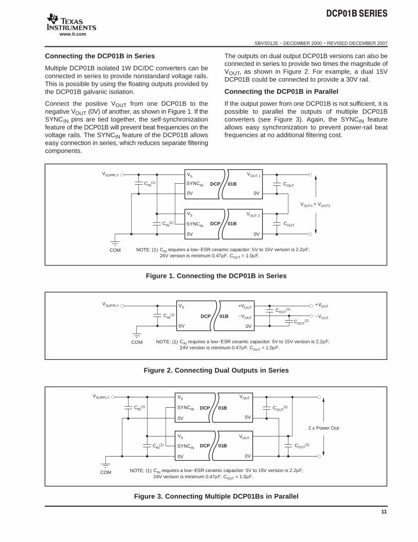
Connecting the DCP01B in Series
Multiple DCP01B isolated 1W DC/DC converters can beconnected in series to provide nonstandard voltage rails.This is possible by using the floating outputs provided bythe DCP01B galvanic isolation.
Connect the positive VOUT from one DCP01B to thenegative VOUT (0V) of another, as shown in Figure 1. If theSYNCIN pins are tied together, the self-synchronizationfeature of the DCP01B will prevent beat frequencies on thevoltage rails. The SYNCIN feature of the DCP01B allowseasy connection in series, which reduces separate filteringcomponents.
The outputs on dual output DCP01B versions can also beconnected in series to provide two times the magnitude ofVOUT, as shown in Figure 2. For example, a dual 15VDCP01B could be connected to provide a 30V rail.
Connecting the DCP01B in Parallel
If the output power from one DCP01B is not sufficient, it ispossible to parallel the outputs of multiple DCP01Bconverters (see Figure 3). Again, the SYNCIN featureallows easy synchronization to prevent power-rail beatfrequencies at no additional filtering cost.
DCP 01B
VOUT 1VSUPPLY VS
0V
DCP 01B
VOUT 2
VOUT1 + VOUT2
SYNCINCIN(1) COUT
COUTCIN(1) SYNCIN
VS
0V
0V
0V
COM NOTE: (1) CIN requires a low−ESR ceramic capacitor: 5V to 15V version is 2.2µF;24V version is minimum 0.47µF. COUT = 1.0µF.
Figure 1. Connecting the DCP01B in Series
DCP 01B
+VOUTVSUPPLY +VOUT
−VOUT−VOUT
0V
VS
0V
COM
COUT(1)
COUT(1)
CIN(1)
NOTE: (1) CIN requires a low−ESR ceramic capacitor: 5V to 15V version is 2.2µF;24V version is minimum 0.47µF. COUT = 1.0µF.
Figure 2. Connecting Dual Outputs in Series
DCP 01B
0V
0V
VOUTVSUPPLY VS
0V
DCP 01B
VOUT
2 x Power Out
SYNCIN
SYNCIN
VS
0V
COM
COUT(1)
COUT(1)
CIN(1)
CIN(1)
NOTE: (1) CIN requires a low−ESR ceramic capacitor: 5V to 15V version is 2.2µF;24V version is minimum 0.47µF. COUT = 1.0µF.
Figure 3. Connecting Multiple DCP01Bs in Parallel
!"#
SBVS012E − DECEMBER 2000 − REVISED DECEMBER 2007
www.ti.com
12
APPLICATION INFORMATIONThe DCP01B, DCV01, and DCP02 are three families ofminiature DC/DC converters providing an isolatedunregulated voltage output. All are fabricated using aCMOS/DMOS process with the DCP01B replacing thefamiliar DCP01 family that was fabricated from a bipolarprocess. The DCP02 is essentially an extension of theDCP01B family providing a higher power output with asignificantly improved load regulation, and the DCV01 istested to a higher isolation voltage.
TRANSFORMER DRIVE CIRCUIT
Transformer drive transistors have a characteristically lowvalue of transistor on resistance (RDS); thus, more poweris transferred to the transformer. The transformer drivecircuit is limited by the base current available to switch onthe power transistors driving the transformer and thecharacteristic current gain (beta), resulting in a slowerturn-on time. Consequently, more power is dissipatedwithin the transistor. This results in a lower overallefficiency, particularly at higher output load currents.
SELF-SYNCHRONIZATION
The input synchronizations facility (SYNCIN), allows foreasy synchronizing of multiple devices. If two to eightdevices (maximum) have their respective SYNCIN pinsconnected together, then all devices will be synchronized.
Each device has its own onboard oscillator. This isgenerated by charging a capacitor from a constant currentand producing a ramp. When this ramp passes athreshold, an internal switch is activated that dischargesthe capacitor to a second threshold before the cycle isrepeated.
When several devices are connected together, all theinternal capacitors are charged simultaneously.
When one device passes its threshold during the chargecycle, it starts the discharge cycle. All the other devicessense this falling voltage and, likewise, initiate a discharge
cycle so that all devices discharge together. A subsequentcharge cycle is only restarted when the last device hasfinished its discharge cycle.
OPTIMIZING PERFORMANCE
Optimum performance can only be achieved if the deviceis correctly supported. By the very nature of a switchingconverter, it requires power to be instantly available whenit switches on. If the converter has DMOS switchingtransistors, the fast edges will create a high currentdemand on the input supply. This transient load placed onthe input is supplied by the external input decouplingcapacitor, thus maintaining the input voltage. Therefore,the input supply does not see this transient (this is ananalogy to high-speed digital circuits). The positioning ofthe capacitor is critical and must be placed as close aspossible to the input pins and connected via alow-impedance path.
The optimum performance is primarily dependent on twofactors:
1. Connection of the input and output circuits forminimal loss.
2. The ability of the decoupling capacitors to maintainthe input and output voltages at a constant level.
PCB Design
The copper losses (resistance and inductance) can beminimized by the use of mutual ground and power planes(tracks) where possible. If that is not possible, use widetracks to reduce the losses. If several devices are beingpowered from a common power source, a star-connectedsystem for the track must be deployed; devices must notbe connected in series, as this will cascade the resistivelosses. The position of the decoupling capacitors isimportant. They must be as close to the devices aspossible in order to reduce losses. See the PCB Layoutsection for more details.
!"#
SBVS012E − DECEMBER 2000 − REVISED DECEMBER 2007
www.ti.com
13
Decoupling Ceramic Capacitors
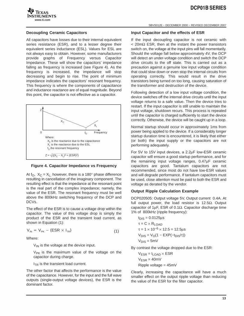
All capacitors have losses due to their internal equivalentseries resistance (ESR), and to a lesser degree theirequivalent series inductance (ESL). Values for ESL arenot always easy to obtain. However, some manufacturersprovide graphs of Frequency versus CapacitorImpedance. These will show the capacitors’ impedancefalling as frequency is increased (see Figure 4). As thefrequency is increased, the impedance will stopdecreasing and begin to rise. The point of minimumimpedance indicates the capacitors’ resonant frequency.This frequency is where the components of capacitanceand inductance reactance are of equal magnitude. Beyondthis point, the capacitor is not effective as a capacitor.
0 fO Frequency
XL
XC
Z
Where:XC is the reactance due to the capacitanceXL is the reactance due to the ESLfO the resonant frequency
Z = √(XC − XL)2 + (ESR)2
Figure 4. Capacitor Impedance vs Frequency
At fO, XC = XL; however, there is a 180° phase differenceresulting in cancellation of the imaginary component. Theresulting effect is that the impedance at the resonant pointis the real part of the complex impedance; namely, thevalue of the ESR. The resonant frequency must be wellabove the 800kHz switching frequency of the DCP andDCVs.
The effect of the ESR is to cause a voltage drop within thecapacitor. The value of this voltage drop is simply theproduct of the ESR and the transient load current, asshown in Equation (1):
VIN VPK (ESR ITR)
Where:
VIN is the voltage at the device input.
VPK is the maximum value of the voltage on thecapacitor during charge.
ITR is the transient load current.
The other factor that affects the performance is the valueof the capacitance. However, for the input and the full waveoutputs (single-output voltage devices), the ESR is thedominant factor.
Input Capacitor and the effects of ESR
If the input decoupling capacitor is not ceramic with< 20mΩ ESR, then at the instant the power transistorsswitch on, the voltage at the input pins will fall momentarily.Should the voltage fall below approximately 4V, the DCPwill detect an under-voltage condition and switch the DCPdrive circuits to the off state. This is carried out as aprecaution against a genuine low input voltage conditionthat could slow down or even stop the internal circuits fromoperating correctly. This would result in the drivetransistors being turned on too long, causing saturation ofthe transformer and destruction of the device.
Following detection of a low input voltage condition, thedevice switches off the internal drive circuits until the inputvoltage returns to a safe value. Then the device tries torestart. If the input capacitor is still unable to maintain theinput voltage, shutdown recurs. This process is repeateduntil the capacitor is charged sufficiently to start the devicecorrectly. Otherwise, the device will be caught up in a loop.
Normal startup should occur in approximately 1ms frompower being applied to the device. If a considerably longerstartup duration time is encountered, it is likely that either(or both) the input supply or the capacitors are notperforming adequately.
For 5V to 15V input devices, a 2.2µF low-ESR ceramiccapacitor will ensure a good startup performance, and forthe remaining input voltage ranges, 0.47µF ceramiccapacitors are good. Tantalum capacitors are notrecommended, since most do not have low-ESR valuesand will degrade performance. If tantalum capacitors mustbe used, close attention must be paid to both the ESR andvoltage as derated by the vendor.
Output Ripple Calculation Example
DCP020505: Output voltage 5V, Output current 0.4A. Atfull output power, the load resistor is 12.5Ω. Outputcapacitor of 1µF, ESR of 0.1Ω. Capacitor discharge time1% of 800kHz (ripple frequency):
tDIS = 0.0125µs
τ = C × RLOAD
τ = 1 × 10−6 × 12.5 = 12.5µs
VDIS = VO(1 − EXP(−tDIS/τ))
VDIS = 5mV
By contrast the voltage dropped due to the ESR:
VESR = ILOAD × ESR
VESR = 40mV
Ripple voltage = 45mV
Clearly, increasing the capacitance will have a muchsmaller effect on the output ripple voltage than reducingthe value of the ESR for the filter capacitor.
(1)
!"#
SBVS012E − DECEMBER 2000 − REVISED DECEMBER 2007
www.ti.com
14
DUAL OUTPUT VOLTAGE DCP AND DCVs
The voltage output for the dual DCPs is half wave rectified;therefore, the discharge time is 1.25µs. Repeating theabove calculations using the 100% load resistance of 25Ω(0.2A per output), the results are shown below:
τ = 25µs
tDIS = 1.25µs.
VDIS = 244mV
VESR = 20mV
Ripple Voltage = 266mV
This time, it is the capacitor discharging that is contributingto the largest component of ripple. Changing the outputfilter to 10µF, and repeating the calculations:
Ripple Voltage = 45mV.
This value is composed of almost equal components.
The above calculations are given only as a guide.Capacitor parameters usually have large tolerances andcan be susceptible to environmental conditions.
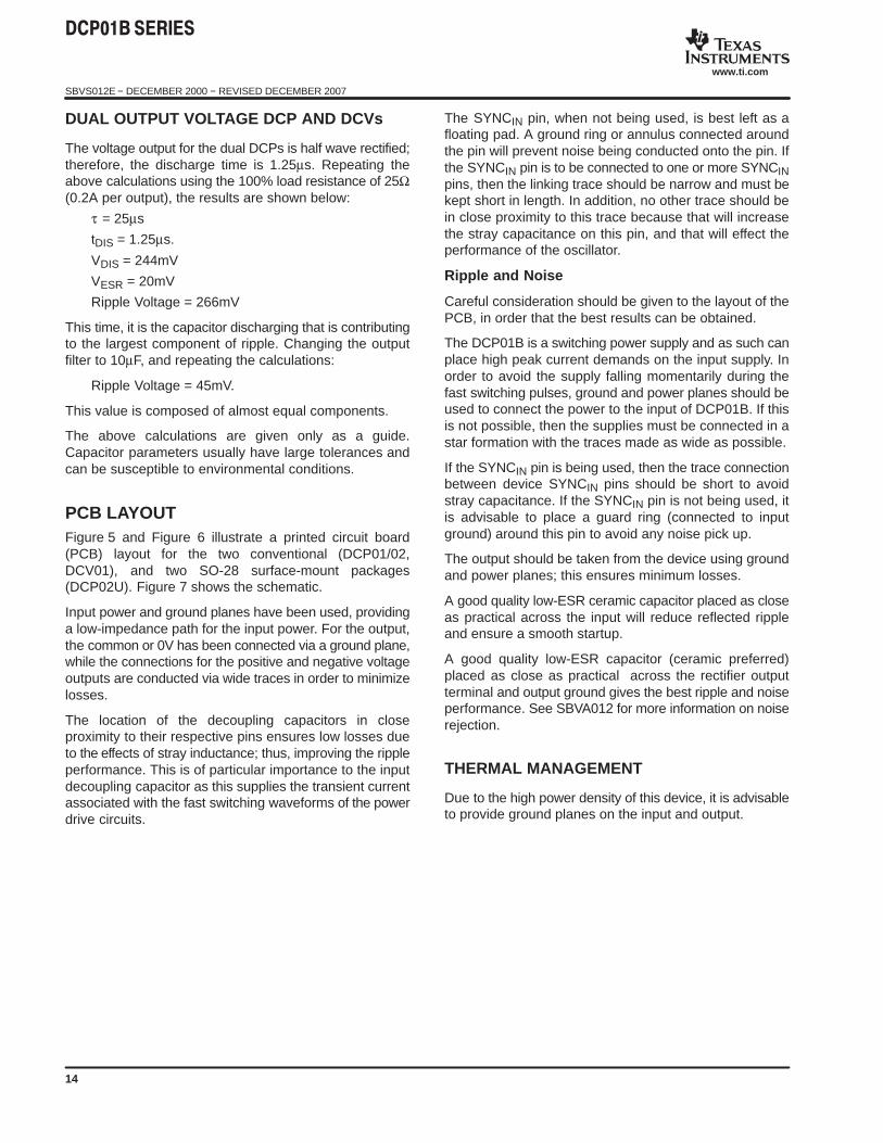
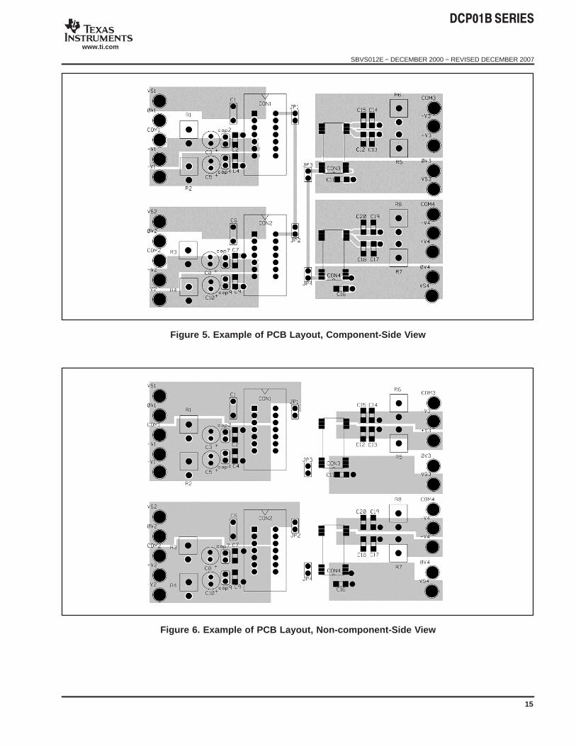
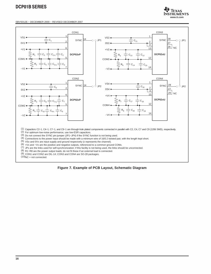
PCB LAYOUTFigure 5 and Figure 6 illustrate a printed circuit board(PCB) layout for the two conventional (DCP01/02,DCV01), and two SO-28 surface-mount packages(DCP02U). Figure 7 shows the schematic.
Input power and ground planes have been used, providinga low-impedance path for the input power. For the output,the common or 0V has been connected via a ground plane,while the connections for the positive and negative voltageoutputs are conducted via wide traces in order to minimizelosses.
The location of the decoupling capacitors in closeproximity to their respective pins ensures low losses dueto the effects of stray inductance; thus, improving the rippleperformance. This is of particular importance to the inputdecoupling capacitor as this supplies the transient currentassociated with the fast switching waveforms of the powerdrive circuits.
The SYNCIN pin, when not being used, is best left as afloating pad. A ground ring or annulus connected aroundthe pin will prevent noise being conducted onto the pin. Ifthe SYNCIN pin is to be connected to one or more SYNCINpins, then the linking trace should be narrow and must bekept short in length. In addition, no other trace should bein close proximity to this trace because that will increasethe stray capacitance on this pin, and that will effect theperformance of the oscillator.
Ripple and Noise
Careful consideration should be given to the layout of thePCB, in order that the best results can be obtained.
The DCP01B is a switching power supply and as such canplace high peak current demands on the input supply. Inorder to avoid the supply falling momentarily during thefast switching pulses, ground and power planes should beused to connect the power to the input of DCP01B. If thisis not possible, then the supplies must be connected in astar formation with the traces made as wide as possible.
If the SYNCIN pin is being used, then the trace connectionbetween device SYNCIN pins should be short to avoidstray capacitance. If the SYNCIN pin is not being used, itis advisable to place a guard ring (connected to inputground) around this pin to avoid any noise pick up.
The output should be taken from the device using groundand power planes; this ensures minimum losses.
A good quality low-ESR ceramic capacitor placed as closeas practical across the input will reduce reflected rippleand ensure a smooth startup.
A good quality low-ESR capacitor (ceramic preferred)placed as close as practical across the rectifier outputterminal and output ground gives the best ripple and noiseperformance. See SBVA012 for more information on noiserejection.
THERMAL MANAGEMENT
Due to the high power density of this device, it is advisableto provide ground planes on the input and output.
!"#
SBVS012E − DECEMBER 2000 − REVISED DECEMBER 2007
www.ti.com
15
Figure 5. Example of PCB Layout, Component-Side View
Figure 6. Example of PCB Layout, Non-component-Side View
!"#
SBVS012E − DECEMBER 2000 − REVISED DECEMBER 2007
www.ti.com
16
(1) Capacitors C2−1, C4−1, C7−1, and C9−1 are through-hole plated components connected in parallel with C2, C4, C7 and C9 (1206 SMD), respectively.(2) For optimum low-noise performance, use low-ESR capacitors.(3) Do not connect the SYNC pin jumper (JP1−JP4) if the SYNC function is not being used.(4) Connections to the power input should be made with a minimum wire of 16/0.2 twisted pair, with the length kept short.(5) VSx and 0Vx are input supply and ground respecively (x represents the channel).(6) +Vx and −Vx are the positive and negative outputs, referenced to a common ground COMx.(7) JPx are the links used for self-synchronization; if this facility is not being used, the links should be unconnected.(8) R1−R8 are the power output loads; do not fit these if an external load is connected.(9) CON1 and CON2 are DIL-14; CON3 and CON4 are SO-28 packages.(10)NC = not connected.
1
23
13
12
14
DCP02xU
28
27
26
C16
R7 C17 C18
R8 C20 C19
VS4
0S4
+V4
COM4
−V4
NC
NC
1
23
13
12
14
C11
R5 C13 C12
R6 C14 C15
VS3
0S3
+V3
COM3
−V3
28
27
26
C1
R1 C3 C2−1 C2
R2 C5 C4−1 C4
VS1
0V1
+V1
COM1
−V1
C6
R3 C8 C7−1 C7
R4 C10 C9−1 C9
VS2
0V2
+V2
COM2
−V2
1
2
6
5
7
1
2
6
5
7
14
14
DCP02xP
SYNC
DCP02xP
SYNC
DCP02xU
SYNC
SYNC
JP1
JP2
JP1
JP2
CON1
CON2
CON3
CON4
Figure 7. Example of PCB Layout, Schematic Diagram
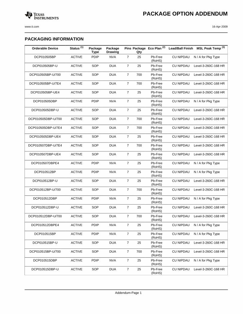
PACKAGING INFORMATION
Orderable Device Status (1) PackageType
PackageDrawing
Pins PackageQty
Eco Plan (2) Lead/Ball Finish MSL Peak Temp (3)
DCP010505BP ACTIVE PDIP NVA 7 25 Pb-Free(RoHS)
CU NIPDAU N / A for Pkg Type
DCP010505BP-U ACTIVE SOP DUA 7 25 Pb-Free(RoHS)
CU NIPDAU Level-3-260C-168 HR
DCP010505BP-U/700 ACTIVE SOP DUA 7 700 Pb-Free(RoHS)
CU NIPDAU Level-3-260C-168 HR
DCP010505BP-U/7E4 ACTIVE SOP DUA 7 700 Pb-Free(RoHS)
CU NIPDAU Level-3-260C-168 HR
DCP010505BP-UE4 ACTIVE SOP DUA 7 25 Pb-Free(RoHS)
CU NIPDAU Level-3-260C-168 HR
DCP010505DBP ACTIVE PDIP NVA 7 25 Pb-Free(RoHS)
CU NIPDAU N / A for Pkg Type
DCP010505DBP-U ACTIVE SOP DUA 7 25 Pb-Free(RoHS)
CU NIPDAU Level-3-260C-168 HR
DCP010505DBP-U/700 ACTIVE SOP DUA 7 700 Pb-Free(RoHS)
CU NIPDAU Level-3-260C-168 HR
DCP010505DBP-U/7E4 ACTIVE SOP DUA 7 700 Pb-Free(RoHS)
CU NIPDAU Level-3-260C-168 HR
DCP010505DBP-UE4 ACTIVE SOP DUA 7 25 Pb-Free(RoHS)
CU NIPDAU Level-3-260C-168 HR
DCP010507DBP-U/7E4 ACTIVE SOP DUA 7 700 Pb-Free(RoHS)
CU NIPDAU Level-3-260C-168 HR
DCP010507DBP-UE4 ACTIVE SOP DUA 7 25 Pb-Free(RoHS)
CU NIPDAU Level-3-260C-168 HR
DCP010507DBPE4 ACTIVE PDIP NVA 7 25 Pb-Free(RoHS)
CU NIPDAU N / A for Pkg Type
DCP010512BP ACTIVE PDIP NVA 7 25 Pb-Free(RoHS)
CU NIPDAU N / A for Pkg Type
DCP010512BP-U ACTIVE SOP DUA 7 25 Pb-Free(RoHS)
CU NIPDAU Level-3-260C-168 HR
DCP010512BP-U/700 ACTIVE SOP DUA 7 700 Pb-Free(RoHS)
CU NIPDAU Level-3-260C-168 HR
DCP010512DBP ACTIVE PDIP NVA 7 25 Pb-Free(RoHS)
CU NIPDAU N / A for Pkg Type
DCP010512DBP-U ACTIVE SOP DUA 7 25 Pb-Free(RoHS)
CU NIPDAU Level-3-260C-168 HR
DCP010512DBP-U/700 ACTIVE SOP DUA 7 700 Pb-Free(RoHS)
CU NIPDAU Level-3-260C-168 HR
DCP010512DBPE4 ACTIVE PDIP NVA 7 25 Pb-Free(RoHS)
CU NIPDAU N / A for Pkg Type
DCP010515BP ACTIVE PDIP NVA 7 25 Pb-Free(RoHS)
CU NIPDAU N / A for Pkg Type
DCP010515BP-U ACTIVE SOP DUA 7 25 Pb-Free(RoHS)
CU NIPDAU Level-3-260C-168 HR
DCP010515BP-U/700 ACTIVE SOP DUA 7 700 Pb-Free(RoHS)
CU NIPDAU Level-3-260C-168 HR
DCP010515DBP ACTIVE PDIP NVA 7 25 Pb-Free(RoHS)
CU NIPDAU N / A for Pkg Type
DCP010515DBP-U ACTIVE SOP DUA 7 25 Pb-Free(RoHS)
CU NIPDAU Level-3-260C-168 HR
PACKAGE OPTION ADDENDUM
www.ti.com 16-Apr-2009
Addendum-Page 1
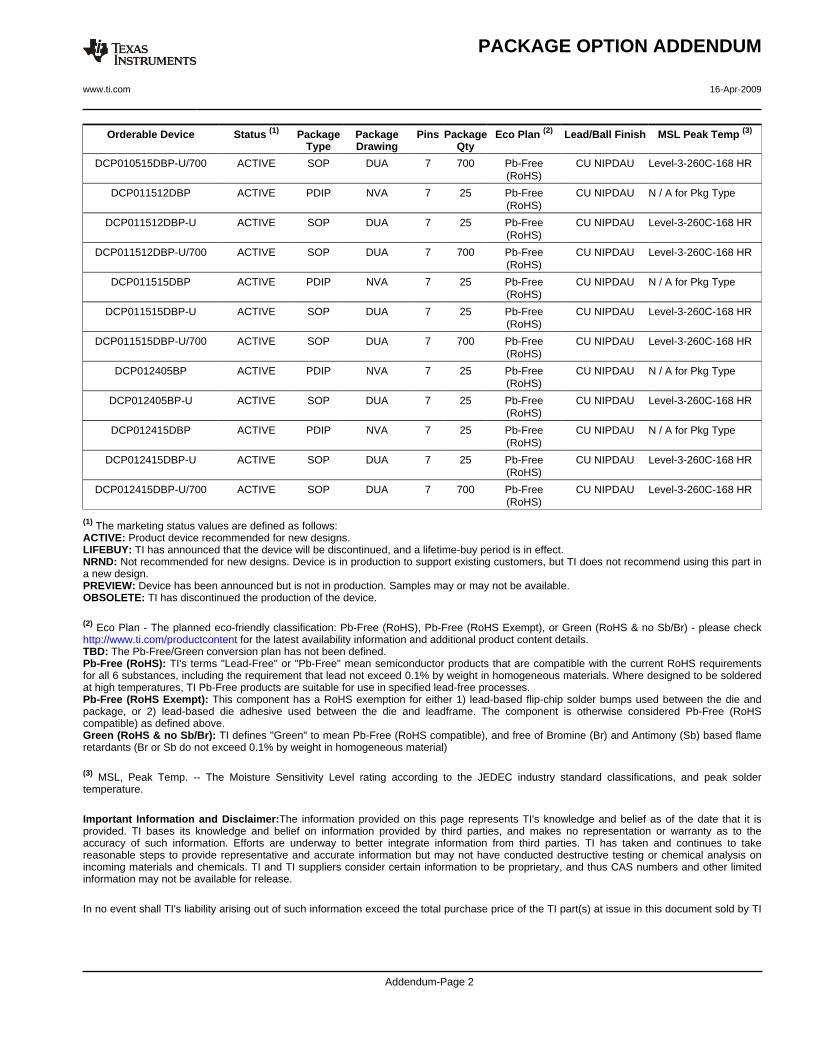
Orderable Device Status (1) PackageType
PackageDrawing
Pins PackageQty
Eco Plan (2) Lead/Ball Finish MSL Peak Temp (3)
DCP010515DBP-U/700 ACTIVE SOP DUA 7 700 Pb-Free(RoHS)
CU NIPDAU Level-3-260C-168 HR
DCP011512DBP ACTIVE PDIP NVA 7 25 Pb-Free(RoHS)
CU NIPDAU N / A for Pkg Type
DCP011512DBP-U ACTIVE SOP DUA 7 25 Pb-Free(RoHS)
CU NIPDAU Level-3-260C-168 HR
DCP011512DBP-U/700 ACTIVE SOP DUA 7 700 Pb-Free(RoHS)
CU NIPDAU Level-3-260C-168 HR
DCP011515DBP ACTIVE PDIP NVA 7 25 Pb-Free(RoHS)
CU NIPDAU N / A for Pkg Type
DCP011515DBP-U ACTIVE SOP DUA 7 25 Pb-Free(RoHS)
CU NIPDAU Level-3-260C-168 HR
DCP011515DBP-U/700 ACTIVE SOP DUA 7 700 Pb-Free(RoHS)
CU NIPDAU Level-3-260C-168 HR
DCP012405BP ACTIVE PDIP NVA 7 25 Pb-Free(RoHS)
CU NIPDAU N / A for Pkg Type
DCP012405BP-U ACTIVE SOP DUA 7 25 Pb-Free(RoHS)
CU NIPDAU Level-3-260C-168 HR
DCP012415DBP ACTIVE PDIP NVA 7 25 Pb-Free(RoHS)
CU NIPDAU N / A for Pkg Type
DCP012415DBP-U ACTIVE SOP DUA 7 25 Pb-Free(RoHS)
CU NIPDAU Level-3-260C-168 HR
DCP012415DBP-U/700 ACTIVE SOP DUA 7 700 Pb-Free(RoHS)
CU NIPDAU Level-3-260C-168 HR
(1) The marketing status values are defined as follows:ACTIVE: Product device recommended for new designs.LIFEBUY: TI has announced that the device will be discontinued, and a lifetime-buy period is in effect.NRND: Not recommended for new designs. Device is in production to support existing customers, but TI does not recommend using this part ina new design.PREVIEW: Device has been announced but is not in production. Samples may or may not be available.OBSOLETE: TI has discontinued the production of the device.
(2) Eco Plan - The planned eco-friendly classification: Pb-Free (RoHS), Pb-Free (RoHS Exempt), or Green (RoHS & no Sb/Br) - please checkhttp://www.ti.com/productcontent for the latest availability information and additional product content details.TBD: The Pb-Free/Green conversion plan has not been defined.Pb-Free (RoHS): TI's terms "Lead-Free" or "Pb-Free" mean semiconductor products that are compatible with the current RoHS requirementsfor all 6 substances, including the requirement that lead not exceed 0.1% by weight in homogeneous materials. Where designed to be solderedat high temperatures, TI Pb-Free products are suitable for use in specified lead-free processes.Pb-Free (RoHS Exempt): This component has a RoHS exemption for either 1) lead-based flip-chip solder bumps used between the die andpackage, or 2) lead-based die adhesive used between the die and leadframe. The component is otherwise considered Pb-Free (RoHScompatible) as defined above.Green (RoHS & no Sb/Br): TI defines "Green" to mean Pb-Free (RoHS compatible), and free of Bromine (Br) and Antimony (Sb) based flameretardants (Br or Sb do not exceed 0.1% by weight in homogeneous material)
(3) MSL, Peak Temp. -- The Moisture Sensitivity Level rating according to the JEDEC industry standard classifications, and peak soldertemperature.
Important Information and Disclaimer:The information provided on this page represents TI's knowledge and belief as of the date that it isprovided. TI bases its knowledge and belief on information provided by third parties, and makes no representation or warranty as to theaccuracy of such information. Efforts are underway to better integrate information from third parties. TI has taken and continues to takereasonable steps to provide representative and accurate information but may not have conducted destructive testing or chemical analysis onincoming materials and chemicals. TI and TI suppliers consider certain information to be proprietary, and thus CAS numbers and other limitedinformation may not be available for release.
In no event shall TI's liability arising out of such information exceed the total purchase price of the TI part(s) at issue in this document sold by TI
PACKAGE OPTION ADDENDUM
www.ti.com 16-Apr-2009
Addendum-Page 2

to Customer on an annual basis.
PACKAGE OPTION ADDENDUM
www.ti.com 16-Apr-2009
Addendum-Page 3
IMPORTANT NOTICETexas Instruments Incorporated and its subsidiaries (TI) reserve the right to make corrections, modifications, enhancements, improvements,and other changes to its products and services at any time and to discontinue any product or service without notice. Customers shouldobtain the latest relevant information before placing orders and should verify that such information is current and complete. All products aresold subject to TI’s terms and conditions of sale supplied at the time of order acknowledgment.TI warrants performance of its hardware products to the specifications applicable at the time of sale in accordance with TI’s standardwarranty. Testing and other quality control techniques are used to the extent TI deems necessary to support this warranty. Except wheremandated by government requirements, testing of all parameters of each product is not necessarily performed.TI assumes no liability for applications assistance or customer product design. Customers are responsible for their products andapplications using TI components. To minimize the risks associated with customer products and applications, customers should provideadequate design and operating safeguards.TI does not warrant or represent that any license, either express or implied, is granted under any TI patent right, copyright, mask work right,or other TI intellectual property right relating to any combination, machine, or process in which TI products or services are used. Informationpublished by TI regarding third-party products or services does not constitute a license from TI to use such products or services or awarranty or endorsement thereof. Use of such information may require a license from a third party under the patents or other intellectualproperty of the third party, or a license from TI under the patents or other intellectual property of TI.Reproduction of TI information in TI data books or data sheets is permissible only if reproduction is without alteration and is accompaniedby all associated warranties, conditions, limitations, and notices. Reproduction of this information with alteration is an unfair and deceptivebusiness practice. TI is not responsible or liable for such altered documentation. Information of third parties may be subject to additionalrestrictions.Resale of TI products or services with statements different from or beyond the parameters stated by TI for that product or service voids allexpress and any implied warranties for the associated TI product or service and is an unfair and deceptive business practice. TI is notresponsible or liable for any such statements.TI products are not authorized for use in safety-critical applications (such as life support) where a failure of the TI product would reasonablybe expected to cause severe personal injury or death, unless officers of the parties have executed an agreement specifically governingsuch use. Buyers represent that they have all necessary expertise in the safety and regulatory ramifications of their applications, andacknowledge and agree that they are solely responsible for all legal, regulatory and safety-related requirements concerning their productsand any use of TI products in such safety-critical applications, notwithstanding any applications-related information or support that may beprovided by TI. Further, Buyers must fully indemnify TI and its representatives against any damages arising out of the use of TI products insuch safety-critical applications.TI products are neither designed nor intended for use in military/aerospace applications or environments unless the TI products arespecifically designated by TI as military-grade or "enhanced plastic." Only products designated by TI as military-grade meet militaryspecifications. Buyers acknowledge and agree that any such use of TI products which TI has not designated as military-grade is solely atthe Buyer's risk, and that they are solely responsible for compliance with all legal and regulatory requirements in connection with such use.TI products are neither designed nor intended for use in automotive applications or environments unless the specific TI products aredesignated by TI as compliant with ISO/TS 16949 requirements. Buyers acknowledge and agree that, if they use any non-designatedproducts in automotive applications, TI will not be responsible for any failure to meet such requirements.Following are URLs where you can obtain information on other Texas Instruments products and application solutions:Products ApplicationsAmplifiers amplifier.ti.com Audio www.ti.com/audioData Converters dataconverter.ti.com Automotive www.ti.com/automotiveDLP® Products www.dlp.com Broadband www.ti.com/broadbandDSP dsp.ti.com Digital Control www.ti.com/digitalcontrolClocks and Timers www.ti.com/clocks Medical www.ti.com/medicalInterface interface.ti.com Military www.ti.com/militaryLogic logic.ti.com Optical Networking www.ti.com/opticalnetworkPower Mgmt power.ti.com Security www.ti.com/securityMicrocontrollers microcontroller.ti.com Telephony www.ti.com/telephonyRFID www.ti-rfid.com Video & Imaging www.ti.com/videoRF/IF and ZigBee® Solutions www.ti.com/lprf Wireless www.ti.com/wireless
Mailing Address: Texas Instruments, Post Office Box 655303, Dallas, Texas 75265Copyright © 2009, Texas Instruments Incorporated