Embed Size (px)
Citation preview

User's GuideSBAU163A–March 2010–Revised April 2010
ADS1259EVM, ADS1259EVM-PDK
ADS1259EVM (Left) and ADS1259EVM-PDK (Right)
This user's guide describes the characteristics, operation, and use of the ADS1259EVM, both by itself andas part of the ADS1259EVM-PDK. This evaluation model (EVM) is an evaluation board for two differentdevices. First, it can be used to evaluate the ADS1259, a low-noise, 24-bit, single-channel, delta-sigma(ΔΣ) analog-to-digital converter (ADC). The ADS1259 can be used either in standalone applications orwith the PGA280. The PGA280 is a high-precision instrumentation amplifier with digitally-controllable gainand signal integrity test capability. The combination of these two devices forms a high-resolutionmeasurement system able to digitize a wide range of signals.
This EVM allows performance evaluations of both the ADS1259 and the PGA280. The EVM also allowsfor PGA280 control of the ADS1259 through the use of the external chip select modes. Complete circuitdescriptions, schematic diagrams, printed circuit board (PCB) layouts, and bill of material are included inthis document.
The following related documents are available through the Texas Instruments web site athttp://www.ti.com.
Related Documents
Device Literature Number
ADS1259 SBAS424A
PGA280 SBOS487A
REF5025 SBOS410C
SN74LVC2G157 SCES207K
ADCPro is a trademark of Texas Instruments.Microsoft, Windows are registered trademarks of Microsoft Corporation.SPI is a trademark of Motorola Inc.I2C is a trademark of NXP Semiconductors.NI-VISA is a trademark of National Instruments.All other trademarks are the property of their respective owners.
1SBAU163A–March 2010–Revised April 2010 ADS1259EVM, ADS1259EVM-PDKSubmit Documentation Feedback
Copyright © 2010, Texas Instruments Incorporated

www.ti.com
Contents1 EVM Overview ............................................................................................................... 42 Analog Interface ............................................................................................................. 43 Digital Interface .............................................................................................................. 64 Power Supplies .............................................................................................................. 75 Voltage Reference .......................................................................................................... 86 ADS1259 Control ........................................................................................................... 97 Clock Source ................................................................................................................ 98 EVM Operation ............................................................................................................ 109 ADS1259EVM-PDK Operation .......................................................................................... 1210 Evaluating Performance with the ADCPro Software .................................................................. 2711 Schematics and Layout ................................................................................................... 35
List of Figures
1 Test Points TP11 and TP12 ............................................................................................... 5
2 Switch S2 and Jumper J15 ................................................................................................ 6
3 Switch S3 .................................................................................................................... 6
4 Jumper J10 .................................................................................................................. 8
5 Switch S1 .................................................................................................................... 8
6 Switch S4 .................................................................................................................... 9
7 ADS1259EVM Default Jumper Positions............................................................................... 11
8 ADS1259EVM Default Switch Positions................................................................................ 11
9 ADS1259EVM-PDK Setup Wizard: Screen 1.......................................................................... 13
10 ADS1259EVM-PDK Setup Wizard: Screen 2.......................................................................... 13
11 ADS1259EVM-PDK Setup Wizard: Screen 3.......................................................................... 14
12 ADS1259EVM-PDK Setup Wizard: Screen 4.......................................................................... 14
13 MMB0 Initial Configuration ............................................................................................... 15
14 Connecting the ADS1259EVM to the MMB0 .......................................................................... 16
15 Using the +6V Wall Supply for +5V ..................................................................................... 17
16 MMB0 Configured for Lab Power Supply .............................................................................. 18
17 NI-VISA Driver Installation Wizard, Screen 1 .......................................................................... 19
18 NI-VISA Driver Installation Wizard, Screen 2 .......................................................................... 20
19 NI-VISA Driver Installation Wizard, Screen 3 .......................................................................... 20
20 NI-VISA Driver Installation Wizard, Screen 4 .......................................................................... 21
21 NI-VISA Driver Verification Using Device Manager ................................................................... 21
22 ADCPro Software Start-up Display Window ........................................................................... 22
23 ADS1259EVM-PDK Plug-In Display Window.......................................................................... 23
24 Install New Driver Wizard Screen 1 ..................................................................................... 24
25 Install New Driver Wizard Screen 2 ..................................................................................... 24
26 Install New Driver Wizard Screen 3 ..................................................................................... 25
27 Install New Driver Wizard Screen 4 ..................................................................................... 25
28 Install New Driver Wizard Screen 5 ..................................................................................... 26
29 USBStyx Driver Verification Using Device Manager.................................................................. 26
30 Data Rate Control ......................................................................................................... 27
31 Over-Range Flag .......................................................................................................... 27
32 ADC Configuration Tab .................................................................................................. 28
33 ADC Calibration Tab ...................................................................................................... 29
34 PGA Configuration Tab ................................................................................................... 30
35 PGA GPIO Tab ............................................................................................................ 31
36 PGA Input Switch Tab .................................................................................................... 32
2 ADS1259EVM, ADS1259EVM-PDK SBAU163A–March 2010–Revised April 2010Submit Documentation Feedback
Copyright © 2010, Texas Instruments Incorporated

www.ti.com
37 PGA Error Indicators Tab ................................................................................................ 33
38 EVM Software About Tab ................................................................................................ 34
39 Software Progress Indicator.............................................................................................. 35
40 Top Silk Image ............................................................................................................. 37
41 Top Side (Layer 1) ........................................................................................................ 37
42 Internal Layer 1 (Layer 2) ................................................................................................ 37
43 Internal Layer 2 (Layer 3) ................................................................................................ 38
44 Bottom Side (Layer 4)..................................................................................................... 38
List of Tables
1 J8: Analog Interface Header Pinout ...................................................................................... 5
2 J7: Serial Data Interface Pins ............................................................................................. 7
3 J11 Configuration: Power-Supply Input .................................................................................. 7
4 ADS1259EVM Bill of Materials .......................................................................................... 35
3SBAU163A–March 2010–Revised April 2010 ADS1259EVM, ADS1259EVM-PDKSubmit Documentation Feedback
Copyright © 2010, Texas Instruments Incorporated

EVM Overview www.ti.com
1 EVM Overview
1.1 Features
ADS1259EVM:• Contains all support circuitry needed for the ADS1259• PGA280 can be evaluated as a buffer and integrated control• Voltage reference options: external or onboard• Clock options: External clock source or 7.3728MHz onboard crystal oscillator• Compatible with the TI Modular EVM System
ADS1259EVM and ADS1259EVM-PDK Features:• Easy-to-use evaluation software for Microsoft® Windows®XP• Data collection to text files• Built-in analysis tools including scope, FFT, and histogram displays• Complete control of board settings• Easily expandable with new analysis plug-in tools from Texas Instruments
For use with a computer, the ADS1259EVM-PDK is available. This kit combines the ADS1259EVM boardwith the DSP-based MMB0 motherboard, and includes ADCPro™ software for evaluation.
The MMB0 motherboard allows the ADS1259EVM to be connected to the computer via an available USBport. This manual shows how to use the MMB0 as part of the ADS1259EVM-PDK, but does not providetechnical details about the MMB0 itself.
ADCPro™ is a program for collecting, recording, and analyzing data from ADC evaluation boards. It isbased on a number of plug-in programs, so it can be expanded easily with new test and data collectionplug-ins. The ADS1259EVM-PDK is controlled by a plug-in running in ADCPro. For more informationabout ADCPro, see the ADCPro™ Analog-to-Digital Converter Evaluation Software User's Guide(SBAU128), available for download from the TI web site.
This manual covers the operation of both the ADS1259EVM and the ADS1259EVM-PDK. Throughout thisdocument, the abbreviation EVM and the term evaluation module are synonymous with theADS1259EVM.
1.2 Introduction
The ADS1259EVM is an evaluation module built to the TI Modular EVM System specification. It can beconnected to any modular EVM system interface card.
The ADS1259EVM is available as a standalone printed circuit board (PCB) or as part of theADS1259EVM-PDK, which includes an MMB0 motherboard and software. As a standalone PCB, theADS1259EVM is useful for prototyping designs and firmware.
Note that the ADS1259EVM has no microprocessor and cannot run software. To connect it to a computer,some type of interface is required.
2 Analog Interface
For maximum flexibility, the ADS1259EVM is designed for easy interfacing to multiple analog sources.Samtec part numbers SSW-110-22-F-D–VS-K and TSM-110-01-T-DV-P provide a convenient 10-pin,dual-row, header/socket combination at J8. This header/socket provides access to the analog input pins ofthe ADS1259 and the PGA280. Consult Samtec at http://www.samtec.com or call 1-800-SAMTEC-9 for avariety of mating connector options.
The input pins on the ADS1259EVM do not connect directly to the part, but connect to the inputs of theADS1259 through switch S2 and modest filtering. Along with the analog header, these analog inputs canbe easily accessed through test loops TP7 and TP8. Analog input pins INN1 and INP1 of the PGA280 canalso be accessed through test loops TP13 and TP14 (INP2 and INN2 can only be accessed through theanalog header). For all analog inputs, it is important that appropriate caution is taken when handling thepins.
4 ADS1259EVM, ADS1259EVM-PDK SBAU163A–March 2010–Revised April 2010Submit Documentation Feedback
Copyright © 2010, Texas Instruments Incorporated

www.ti.com Analog Interface
Table 1 summarizes the pinouts for analog interface header J8.
Table 1. J8: Analog Interface Header Pinout
Pin Number Signal Description
J8.1 A0N AINN, ADS1259, through switch S2 and low-passfilter, R1-2, C1-3
J8.2 A0P AINP, ADS1259, through switch S2 and low-passfilter, R1-2, C1-3
J8.3 A1N INN1, PGA280, through R7
J8.4 A1P INP1, PGA280, through R6
J8.5 A1N INN2, PGA280, through R5
J8.6 A1P INP2, PGA280, through R4
J8.9-13 (odd) AGND Analog ground connections
J8.15 VCOM VOCM, PGA280, via switch S3 and R3
J8.17-19 (odd) AGND Analog ground connections
J8.18 REFN External reference source input (– side ofdifferential input)
J8.20 REFP External reference source input (+ side ofdifferential input)
J8.10-16 (even) Unused —
The output pins of the PGA280 (VOP and VON) can be accessed through TP11 and TP12, but there is noconnection to the analog interface J8. Figure 1 shows TP11 and TP12.
Figure 1. Test Points TP11 and TP12
The input of the ADS1259 is selectable through switch S2. From settings left-to-right, this three-way switchselects the ADC input from the AINP or AINN inputs from the analog interface header, the VOP and VONoutputs of the PGA280, or allows for the self calibration inputs in combination with jumper J15.
5SBAU163A–March 2010–Revised April 2010 ADS1259EVM, ADS1259EVM-PDKSubmit Documentation Feedback
Copyright © 2010, Texas Instruments Incorporated

Digital Interface www.ti.com
As an indicator, the three settings of S2 are labeled HDR, PGA, and CAL below the switch, as Figure 2illustrates.
Figure 2. Switch S2 and Jumper J15
When switch S2 is set to the right, jumper J15 is used in the system calibration modes for the ADS1259.When the jumper is set to the left, pins 1 and 2 of jumper J15 are connected. The inputs of the ADS1259are shorted together and tied to REFP. With this connection, the user can run an offset calibration. Whenthe jumper is set to the right, pins 2 and 3 of jumper J15 are connected. The inputs of the ADS1259 aretied to REFP and REFN, measuring the reference voltage. At this point, the user can run a gaincalibration. On either side of J15, OF and GA indicate the sides of jumper J15 used for offset and gaincalibrations.
Another three-way switch (S3) sets the source of the output common-mode of the PGA280. Setting theswitch to the left connects the output common-mode to pin J8.15 of the analog interface header. Thecenter setting of the switch connects it to the midpoint between AVDD and AVSS via the voltage divider ofR8 and R9. The right setting connects it to the REFOUT of the ADS1259. These options are labeled underthe switch as HDR, AVDD/2, and REF respectively. Figure 3 shows S3 as it appears on theADS1259EVM.
Figure 3. Switch S3
3 Digital Interface
The ADS1259EVM is designed to easily interface with multiple control platforms. Samtec part numbersSSW-110-22-F-D–VS-K and TSM-110-01-T-DV-P provide a convenient 10-pin, dual-row, header/socketcombination at J7. This header/socket provides access to the digital control and serial data pins of theADC. Consult Samtec at http://www.samtec.com or call 1-800-SAMTEC-9 for a variety of matingconnector options.
6 ADS1259EVM, ADS1259EVM-PDK SBAU163A–March 2010–Revised April 2010Submit Documentation Feedback
Copyright © 2010, Texas Instruments Incorporated

www.ti.com Power Supplies
All logic levels on J7 are 3.3V CMOS, except for the I2C™ pins. These pins conform to 3.3V I2C rules.Table 2 describes the J7 serial interface pins.
Table 2. J7: Serial Data Interface Pins
Pin No. Pin Name Signal Name I/O Type Pull-up Function
J7.1 CNTL Unused — — —
J7.2 GPIO0 START In High ADS1259 START Pin
J7.3 CLKX SCLK In None ADS1259/PGA280 SPI clock
J7.4 DGND DGND In/Out None Digital Ground
J7.5 CLKR Unused — — —
J7.6 GPIO1 RST/PDWN In High ADS1259 RST/PDWN
J7.7 FSX CS — — ADS1259 SPI Chip Select
J7.8 GPIO2 DOUT Out High PGA280 SPI data out
J7.9 FSR Unused — None —
J7.10 DGND DGND In/Out None Digital Ground
J7.11 DX DIN In None ADS1259 SPI data in
J7.12 GPIO3 CS In High PGA280 SPI Chip Select
J7.13 DR DOUT Out None ADS1259 SPI data out
J7.14 GPIO4 Unused — None —
J7.15 INT DRDY Out None ADS1259 SPI Data Ready signal
J7.16 SCL SCL I2C n/a I2C clock
J7.17 TOUT CLK In None Can be used to provide a clock froma processor
J7.18 DGND DGND In/Out None Digital Ground
J7.19 GPIO5 EXTCLK In None External Clock input
J7.20 SDA SDA I2C n/a I2C data
Many pins on J7 have weak pull-up/-down resistors. These resistors provide default settings for many ofthe control pins. Furthermore, many pins on J7 correspond directly to pins on the ADS1259. See theADS1259 product data sheet for complete details on these pins.
4 Power Supplies
J11 is the power-supply input connector. Table 3 lists the configuration details for J11. The ADS1259 andPGA280 output amplifier are powered from +5V that can be supplied through the +5VA supply that can befound on pin J11.3. An additional bipolar supply is needed to power the PGA280 through +VA and –VAthrough pins J11.1 and J11.2.
Table 3. J11 Configuration: Power-Supply Input
Pin No. Pin Name Function Required
J11.1 +VA +10V to +15V Yes
J11.2 –VA -10V to -15V Yes
J11.3 +5VA +5V analog supply Always
J11.4 -5VA -5V analog supply No
J11.5 DGND Digital ground input Yes
J11.6 AGND Analog ground input Yes
J11.7 +1.8VD 1.8V digital supply No
J11.8 VD1 Not used No
J11.9 +3.3VD 3.3V digital supply Always
J11.10 +5VD +5V No
7SBAU163A–March 2010–Revised April 2010 ADS1259EVM, ADS1259EVM-PDKSubmit Documentation Feedback
Copyright © 2010, Texas Instruments Incorporated
Voltage Reference www.ti.com
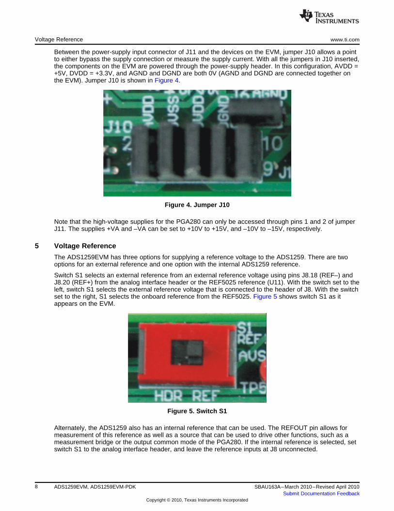
Between the power-supply input connector of J11 and the devices on the EVM, jumper J10 allows a pointto either bypass the supply connection or measure the supply current. With all the jumpers in J10 inserted,the components on the EVM are powered through the power-supply header. In this configuration, AVDD =+5V, DVDD = +3.3V, and AGND and DGND are both 0V (AGND and DGND are connected together onthe EVM). Jumper J10 is shown in Figure 4.
Figure 4. Jumper J10
Note that the high-voltage supplies for the PGA280 can only be accessed through pins 1 and 2 of jumperJ11. The supplies +VA and –VA can be set to +10V to +15V, and –10V to –15V, respectively.
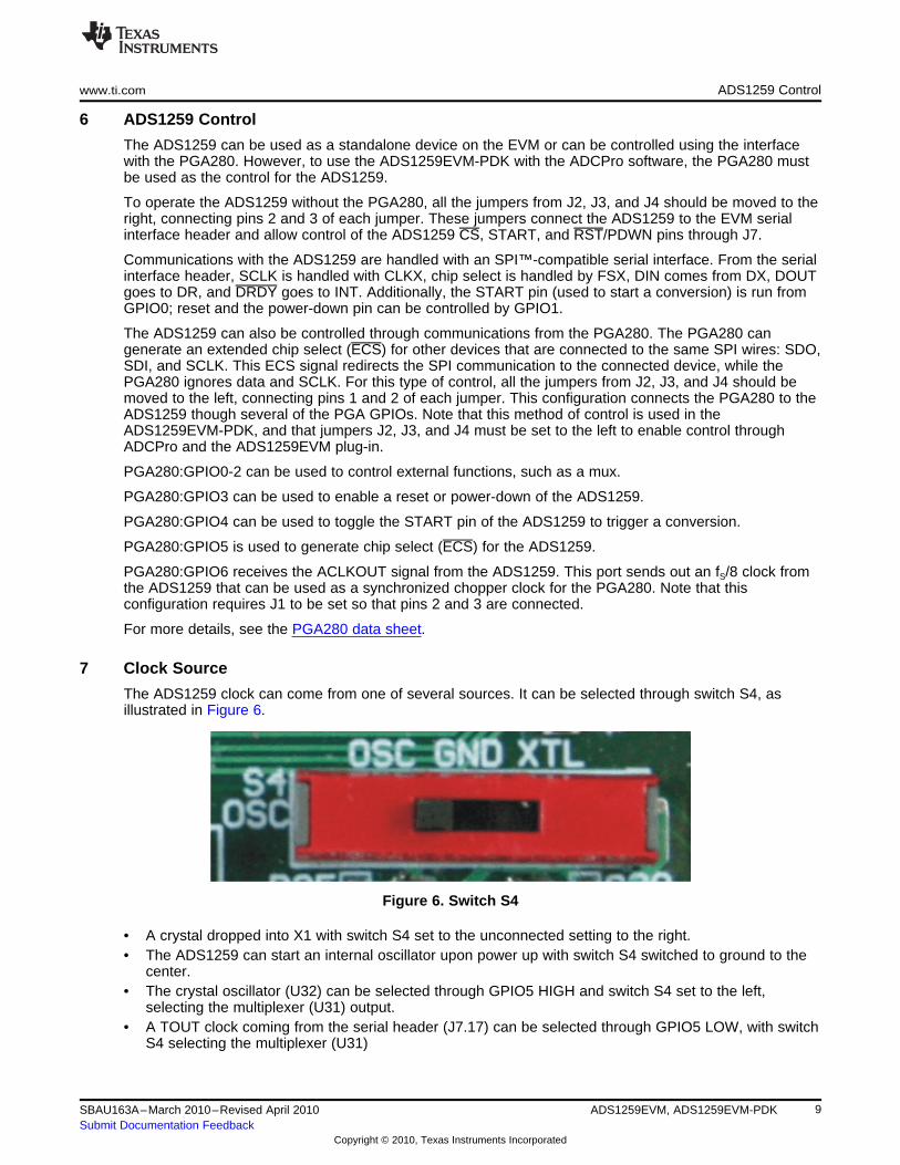
5 Voltage Reference
The ADS1259EVM has three options for supplying a reference voltage to the ADS1259. There are twooptions for an external reference and one option with the internal ADS1259 reference.
Switch S1 selects an external reference from an external reference voltage using pins J8.18 (REF–) andJ8.20 (REF+) from the analog interface header or the REF5025 reference (U11). With the switch set to theleft, switch S1 selects the external reference voltage that is connected to the header of J8. With the switchset to the right, S1 selects the onboard reference from the REF5025. Figure 5 shows switch S1 as itappears on the EVM.
Figure 5. Switch S1
Alternately, the ADS1259 also has an internal reference that can be used. The REFOUT pin allows formeasurement of this reference as well as a source that can be used to drive other functions, such as ameasurement bridge or the output common mode of the PGA280. If the internal reference is selected, setswitch S1 to the analog interface header, and leave the reference inputs at J8 unconnected.
8 ADS1259EVM, ADS1259EVM-PDK SBAU163A–March 2010–Revised April 2010Submit Documentation Feedback
Copyright © 2010, Texas Instruments Incorporated
www.ti.com ADS1259 Control
6 ADS1259 Control
The ADS1259 can be used as a standalone device on the EVM or can be controlled using the interfacewith the PGA280. However, to use the ADS1259EVM-PDK with the ADCPro software, the PGA280 mustbe used as the control for the ADS1259.
To operate the ADS1259 without the PGA280, all the jumpers from J2, J3, and J4 should be moved to theright, connecting pins 2 and 3 of each jumper. These jumpers connect the ADS1259 to the EVM serialinterface header and allow control of the ADS1259 CS, START, and RST/PDWN pins through J7.
Communications with the ADS1259 are handled with an SPI™-compatible serial interface. From the serialinterface header, SCLK is handled with CLKX, chip select is handled by FSX, DIN comes from DX, DOUTgoes to DR, and DRDY goes to INT. Additionally, the START pin (used to start a conversion) is run fromGPIO0; reset and the power-down pin can be controlled by GPIO1.
The ADS1259 can also be controlled through communications from the PGA280. The PGA280 cangenerate an extended chip select (ECS) for other devices that are connected to the same SPI wires: SDO,SDI, and SCLK. This ECS signal redirects the SPI communication to the connected device, while thePGA280 ignores data and SCLK. For this type of control, all the jumpers from J2, J3, and J4 should bemoved to the left, connecting pins 1 and 2 of each jumper. This configuration connects the PGA280 to theADS1259 though several of the PGA GPIOs. Note that this method of control is used in theADS1259EVM-PDK, and that jumpers J2, J3, and J4 must be set to the left to enable control throughADCPro and the ADS1259EVM plug-in.
PGA280:GPIO0-2 can be used to control external functions, such as a mux.
PGA280:GPIO3 can be used to enable a reset or power-down of the ADS1259.
PGA280:GPIO4 can be used to toggle the START pin of the ADS1259 to trigger a conversion.
PGA280:GPIO5 is used to generate chip select (ECS) for the ADS1259.
PGA280:GPIO6 receives the ACLKOUT signal from the ADS1259. This port sends out an fS/8 clock fromthe ADS1259 that can be used as a synchronized chopper clock for the PGA280. Note that thisconfiguration requires J1 to be set so that pins 2 and 3 are connected.
For more details, see the PGA280 data sheet.
7 Clock Source
The ADS1259 clock can come from one of several sources. It can be selected through switch S4, asillustrated in Figure 6.
Figure 6. Switch S4
• A crystal dropped into X1 with switch S4 set to the unconnected setting to the right.• The ADS1259 can start an internal oscillator upon power up with switch S4 switched to ground to the
center.• The crystal oscillator (U32) can be selected through GPIO5 HIGH and switch S4 set to the left,
selecting the multiplexer (U31) output.• A TOUT clock coming from the serial header (J7.17) can be selected through GPIO5 LOW, with switch
S4 selecting the multiplexer (U31)
9SBAU163A–March 2010–Revised April 2010 ADS1259EVM, ADS1259EVM-PDKSubmit Documentation Feedback
Copyright © 2010, Texas Instruments Incorporated

EVM Operation www.ti.com
7.1 Usage in PDK
If using the ADS1259EVM as part of the ADS1259EVM-PDK, switch S4 should be set to the left, using themultiplexer output. Using the onboard 7.3728MHz crystal oscillator allows the ADS1259EVM-PDKsoftware to recognize the EVM using the software provided.
7.2 Usage as a standalone EVM
If using the EVM in your own system and not with the PDK hardware and software, switch S4 can be usedto select the clock. The switch can be used to select the 7.3728MHz crystal (through multiplexer U31) orto allow the onboard oscillator to be enabled when S4 is set to ground.
8 EVM Operation
This section provides information on the analog input, digital control, and general operating conditions ofthe ADS1259EVM.
8.1 Analog Input
A single-channel differential input source can be applied directly to J8 (top or bottom side) or throughsignal-conditioning modules available for the modular EVM system. The input is connected through switchS2 and through a low-pass filter (R1, R2, C10, C11, and C12) before reaching the ADS1259.
The common-mode voltage (VCOM) for the PGA280 input buffer is 2.5V supplied from the REFOUT of theADS1259, the VCOM pin at the analog header (J8.15), or a voltage divider set to AVDD/2. Thisconfiguration can be selected through switch S3.
8.2 Digital Control
The digital control signals can be applied directly to J7 (top or bottom side). The modular ADS1259EVMcan also be connected directly to a DSP or microcontroller interface board, such as the 5-6k Interface orHPA-MCU Interface boards available from Texas Instruments, or the MMB0 if purchased as part of theADS1259EVM-PDK. For a list of compatible interface and/or accessory boards for the EVM or theADS1259, see the relevant product folder on the TI web site. Some of the digital signals are controlleddirectly with pins on J7.
Other pins on the ADS1259 may be accessed via J7 through J2, J3, and J4. The ADS1259EVM-PDKuses the PGA280 external chip select function to control the ADS1259; therefore, these jumpers must beset to allow for access through J7.
10 ADS1259EVM, ADS1259EVM-PDK SBAU163A–March 2010–Revised April 2010Submit Documentation Feedback
Copyright © 2010, Texas Instruments Incorporated

www.ti.com EVM Operation
8.3 Default Jumper Settings and Switch Positions
Jumpers connect the power supplies and enable PGA280 control of the ADS1259. J1, J2, J3, and J4 areall set to the left and connect the PGA280 to ADS1259. All the jumpers on J6 and J10 are used to connectpower supplies and grounds. J15 is used to short the inputs together during an offset calibration. Figure 7shows the jumpers found on the EVM and the respective factory default conditions for each.
Figure 7. ADS1259EVM Default Jumper Positions
Four switches are used on the ADS1259/PGA280. Three-way switch S1 is set to the center position,setting the output common-mode of the PGA280 to AVDD/2. Switch S2 is set to the right, connecting theADS1259 reference to the EVM onboard reference. Three-way switch S3 is set to the right to allow forcalibration of the ADS1259, through jumper J15. Finally, three-way switch S4 is set to the left connectingthe ADS1259 to the onboard oscillator. Figure 8 illustrates the switches on the EVM and the respectivefactory default configurations for each.
Figure 8. ADS1259EVM Default Switch Positions
11SBAU163A–March 2010–Revised April 2010 ADS1259EVM, ADS1259EVM-PDKSubmit Documentation Feedback
Copyright © 2010, Texas Instruments Incorporated

ADS1259EVM-PDK Operation www.ti.com
9 ADS1259EVM-PDK Operation
This section provides information on using the ADS1259EVM-PDK, including setup, program installation,and program usage.
To prepare to evaluate the ADS1259 with the ADS1259EVM-PDK, complete the following steps:
Step 1. Install the ADCPro software (if not already installed) on a PC.Step 2. Install the ADS1259EVM-PDK EVM plug-in software.Step 3. Set up the ADS1259EVM-PDK.Step 4. Connect a proper power supply or use the included AC adapter.Step 5. Complete the NI-VISA™ USB driver installation process.Step 6. Run the ADCPro software.Step 7. Complete the Microsoft Windows USB driver installation process.
Each task is described in the subsequent sections of this document.
9.1 Installing the ADCPro Software
CAUTION
Do not connect the ADS1259EVM-PDK before installing the software on asuitable PC. Failure to observe this caution may cause Microsoft Windows tonot recognize the ADS1259EVM-PDK.
The latest software is available from the TI website at http://www.ti.com. The CD-ROM shipped with theADS1259EVM may not contain the latest software, but the ADCPro installer will check for updates whenexecuted (if connected to the Internet), and then give you the option of downloading and installing thelatest version. Refer to the ADCPro User's Guide for instructions on installing and using ADCPro.
To install the ADS1259EVM-PDK plug-in, run the file: ADS1259EVM-pdk-plug-in-1.0.0.exe (1.0.0 is theversion number, and increments with software version releases; you may have a different version on yourCD). Double-click the file to run it; then follow the instructions shown. You can also utilize the ADCProUpdate Check feature to check for newer versions of the ADS1259EVM-PDK plug-in, once you haveinstalled one version of it.
Installation for the ADS1259EVM plug-in should be relatively straightforward. The plug-in comes as anexecutable file. Once started, the program leads the user through the screens shown in Figure 9 throughFigure 12.
12 ADS1259EVM, ADS1259EVM-PDK SBAU163A–March 2010–Revised April 2010Submit Documentation Feedback
Copyright © 2010, Texas Instruments Incorporated

www.ti.com ADS1259EVM-PDK Operation
Figure 9. ADS1259EVM-PDK Setup Wizard: Screen 1
Figure 10. ADS1259EVM-PDK Setup Wizard: Screen 2
13SBAU163A–March 2010–Revised April 2010 ADS1259EVM, ADS1259EVM-PDKSubmit Documentation Feedback
Copyright © 2010, Texas Instruments Incorporated

ADS1259EVM-PDK Operation www.ti.com
Figure 11. ADS1259EVM-PDK Setup Wizard: Screen 3
Figure 12. ADS1259EVM-PDK Setup Wizard: Screen 4
The software should now be installed, but the USB drivers may not yet have been loaded by the PCoperating system. This step completes when the ADCPro software is executed; see Section 9.4, Runningthe Software and Completing Driver Installation.
14 ADS1259EVM, ADS1259EVM-PDK SBAU163A–March 2010–Revised April 2010Submit Documentation Feedback
Copyright © 2010, Texas Instruments Incorporated

www.ti.com ADS1259EVM-PDK Operation
9.2 Setting Up the ADS1259EVM-PDK
The ADS1259EVM-PDK contains both the ADS1259EVM and the MMB0 motherboard; however, thedevices are shipped unconnected. Follow these steps to set up the ADS1259EVM-PDK:
Step 1. Unpack the ADS1259EVM-PDK package.Step 2. Set the jumpers and switches on the MMB0 as shown in Figure 13.
• Set the Boot Mode switch to USB.• Connect +5V and +5VA on jumper block J13 (if +5V is supplied from J14 +5VA).• Leave +5V and +5VA disconnected on jumper block J13.• If the PDK will be powered from an ac adapter, connect J12. If the PDK will be powered
through the terminal block, disconnect J12 (see Section 9.3 for details on connecting thepower supply).
Figure 13. MMB0 Initial Configuration
15SBAU163A–March 2010–Revised April 2010 ADS1259EVM, ADS1259EVM-PDKSubmit Documentation Feedback
Copyright © 2010, Texas Instruments Incorporated
ADS1259EVM-PDK Operation www.ti.com
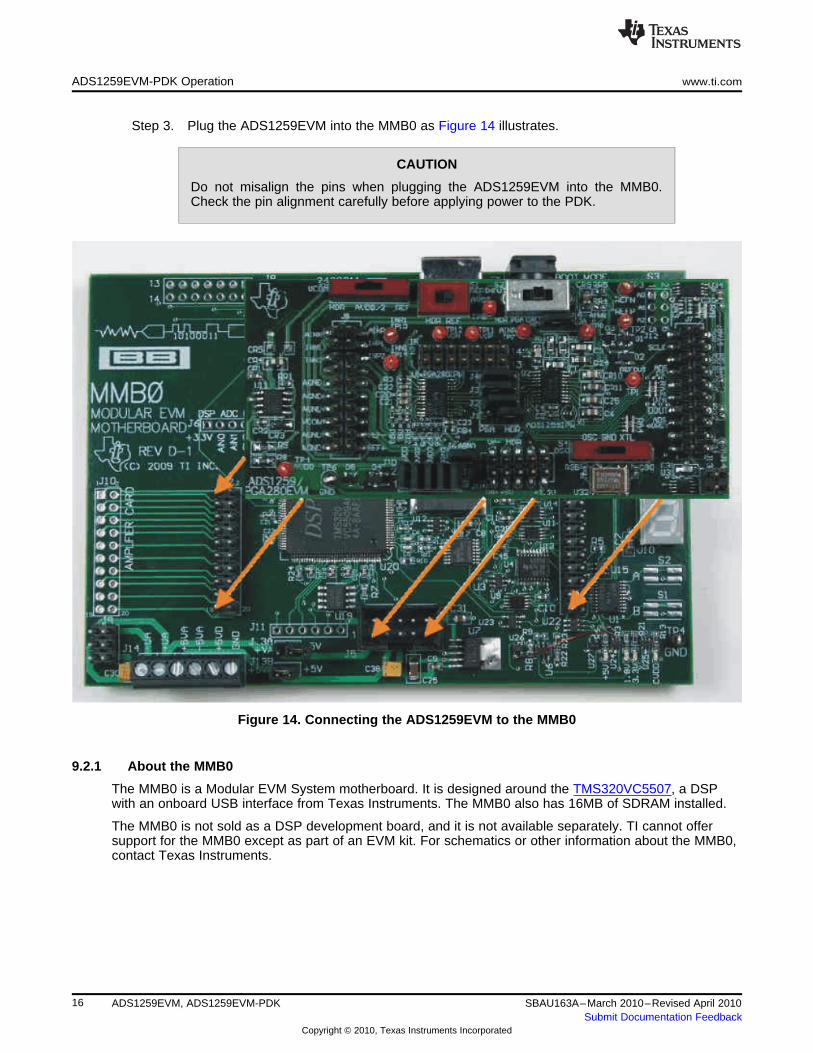
spaceStep 3. Plug the ADS1259EVM into the MMB0 as Figure 14 illustrates.
CAUTION
Do not misalign the pins when plugging the ADS1259EVM into the MMB0.Check the pin alignment carefully before applying power to the PDK.
Figure 14. Connecting the ADS1259EVM to the MMB0
9.2.1 About the MMB0
The MMB0 is a Modular EVM System motherboard. It is designed around the TMS320VC5507, a DSPwith an onboard USB interface from Texas Instruments. The MMB0 also has 16MB of SDRAM installed.
The MMB0 is not sold as a DSP development board, and it is not available separately. TI cannot offersupport for the MMB0 except as part of an EVM kit. For schematics or other information about the MMB0,contact Texas Instruments.
16 ADS1259EVM, ADS1259EVM-PDK SBAU163A–March 2010–Revised April 2010Submit Documentation Feedback
Copyright © 2010, Texas Instruments Incorporated

J13
POWER
SUPPLY
CONFIG
J12
WALL SUPPLY CONNECTION
J2
AC ADAPTER INPUT
J14
POWER
INPUT +10V
-10V
www.ti.com ADS1259EVM-PDK Operation
9.3 Connecting the Power Supply
The ADS1259EVM-PDK can be operated with a combination of +5V and bipolar (±10V to ±15V) supply.
When the MMB0 DSP is powered properly, LED D2 glows green. The green light indicates that the 3.3Vsupply for the MMB0 is operating properly. (It does not indicate that the EVM power supplies areoperating properly.)
9.3.1 Using the +6V Wall Supply for +5V
An ac adapter can be connected to barrel jack J2 on the MMB0. J2 is located next to the USB connector.The adapter must output 6V to 7V dc. The connector must be sleeve-negative, tip-positive. It should havea current rating of at least 2A.
Jumper J12 on the MMB0 connects a wall-mounted power supply to the board. To use the wall-mountsupply, J12 must be shorted. Figure 15 illustrates how to connect an ac adapter to the MMB0.
Figure 15. Using the +6V Wall Supply for +5V
17SBAU163A–March 2010–Revised April 2010 ADS1259EVM, ADS1259EVM-PDKSubmit Documentation Feedback
Copyright © 2010, Texas Instruments Incorporated

J13
POWER
SUPPLY
CONFIG
J14
POWER
INPUT
J12
WALL SUPPLY DISCONNECT
GND+5VDC
(OPTIONAL) 5VDC-
+10V-10V
ADS1259EVM-PDK Operation www.ti.com
9.3.2 Using an External Supply for +5V
A laboratory power supply can be connected through terminal block J14 on the MMB0, as shown inFigure 16. Both unipolar and bipolar configurations are supported.
Figure 16. MMB0 Configured for Lab Power Supply
To use a lab power-supply configuration:
• Disconnect J12 on the MMB0.• Connect a +5V dc supply to the +5VA terminal on J14.• Connect ground of the dc supply to the GND terminal on J14.• Connect a –10V dc supply to the –VA, and +10V on the +VA terminals on J14.
For bipolar mode, connect at –5V supply to –5VA.
It is not necessary to connect a +5V dc supply voltage to the +5VA terminal on J14 if the +5V/+5VAposition on J13 is shorted.
18 ADS1259EVM, ADS1259EVM-PDK SBAU163A–March 2010–Revised April 2010Submit Documentation Feedback
Copyright © 2010, Texas Instruments Incorporated

www.ti.com ADS1259EVM-PDK Operation
9.4 Running the Software and Completing Driver Installation
NOTE: The software is continually under development. These instructions and screen images arecurrent at the time of this writing, but may not exactly match future releases.
The program for evaluating the ADS1259EVM-PDK is called ADCPro. This program uses plug-ins tocommunicate with the EVM. The ADS1259EVM-PDK plug-in is included in the ADS1259EVM-PDKpackage.
The program currently runs only on Microsoft Windows platforms of Windows XP; Windows Vista andWindows 7 are NOT supported.
If this is the first time installing ADCPro and plug-ins, follow these procedures to run ADCPro andcomplete the necessary driver installation. Make sure the ADCPro software and device plug-in softwareare installed from the CD-ROM as described in Section 9.1.
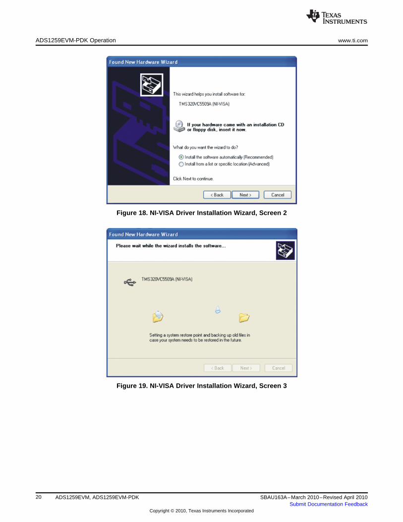
9.4.1 NI-VISA USB Device Driver Installation1. After the ADCPro software is installed, apply power to the PDK and connect the board to an available
PC USB port.2. The computer should recognize new hardware and begin installing the drivers for the hardware.
Figure 17 through Figure 20 are provided for reference to show the installation steps.
• For the first screen, Figure 17, it is not necessary to search for the software; it has already beeninstalled on your PC.
• For the remaining steps, accept the default settings.
Figure 17. NI-VISA Driver Installation Wizard, Screen 1
19SBAU163A–March 2010–Revised April 2010 ADS1259EVM, ADS1259EVM-PDKSubmit Documentation Feedback
Copyright © 2010, Texas Instruments Incorporated
ADS1259EVM-PDK Operation www.ti.com
Figure 18. NI-VISA Driver Installation Wizard, Screen 2
Figure 19. NI-VISA Driver Installation Wizard, Screen 3
20 ADS1259EVM, ADS1259EVM-PDK SBAU163A–March 2010–Revised April 2010Submit Documentation Feedback
Copyright © 2010, Texas Instruments Incorporated

www.ti.com ADS1259EVM-PDK Operation
Figure 20. NI-VISA Driver Installation Wizard, Screen 4
This procedure should complete the installation of the NI-VISA drivers. You can verify proper installationby opening the Windows Device Manager and locating the drivers as shown in Figure 21.
Figure 21. NI-VISA Driver Verification Using Device Manager
21SBAU163A–March 2010–Revised April 2010 ADS1259EVM, ADS1259EVM-PDKSubmit Documentation Feedback
Copyright © 2010, Texas Instruments Incorporated

ADS1259EVM-PDK Operation www.ti.com
9.4.2 USBStyx Driver Installation1. Start the software by selecting ADCPro from the Windows Start menu. The screen in Figure 22
appears.
Figure 22. ADCPro Software Start-up Display Window
22 ADS1259EVM, ADS1259EVM-PDK SBAU163A–March 2010–Revised April 2010Submit Documentation Feedback
Copyright © 2010, Texas Instruments Incorporated

www.ti.com ADS1259EVM-PDK Operation
space2. Select ADS1259EVM from the EVM drop-down menu. The ADS1259EVM-PDK plug-in appears in the
left pane, as shown in Figure 23.
Figure 23. ADS1259EVM-PDK Plug-In Display Window
3. The ADS1259EVM-PDK plug-in window has a status area at the top of the screen. When the plug-in isfirst loaded, the plug-in searches for the board. You will see a series of messages in the status areaindicating this action.
4. If you have not yet loaded the operating system drivers, Windows will display the Windows Install NewDriver Wizard sequence (illustrated in Figure 24 through Figure 28). Accept the default settings.
NOTE: During the driver installation, a message may appear indicating the firmware load hasTIMED OUT. Click OK and continue driver installation. The plug-in attempts to download thefirmware again once the driver installation completes.
23SBAU163A–March 2010–Revised April 2010 ADS1259EVM, ADS1259EVM-PDKSubmit Documentation Feedback
Copyright © 2010, Texas Instruments Incorporated

ADS1259EVM-PDK Operation www.ti.com
Figure 24. Install New Driver Wizard Screen 1
Figure 25. Install New Driver Wizard Screen 2
24 ADS1259EVM, ADS1259EVM-PDK SBAU163A–March 2010–Revised April 2010Submit Documentation Feedback
Copyright © 2010, Texas Instruments Incorporated

www.ti.com ADS1259EVM-PDK Operation
Figure 26. Install New Driver Wizard Screen 3
Figure 27. Install New Driver Wizard Screen 4
25SBAU163A–March 2010–Revised April 2010 ADS1259EVM, ADS1259EVM-PDKSubmit Documentation Feedback
Copyright © 2010, Texas Instruments Incorporated

ADS1259EVM-PDK Operation www.ti.com
Figure 28. Install New Driver Wizard Screen 5
5. Once Windows finishes installing the software driver, the plug-in downloads the firmware to the MMB0.The status area displays Connected to EVM when the device is connected and ready to use. If thefirmware does not load properly, you can try resetting the MMB0 by pressing Reset and then reloadingthe plug-in.
6. You can verify the proper installation of the USBStyx driver using the Device Manager. Note that thefirst driver item, NI-VISA USB Devices, disappears and a new item, LibUSB-Win32 Devices appears,as Figure 29 shows.
Figure 29. USBStyx Driver Verification Using Device Manager
The driver installation wizard sequence should not appear again, unless you connect the board to adifferent USB port.
26 ADS1259EVM, ADS1259EVM-PDK SBAU163A–March 2010–Revised April 2010Submit Documentation Feedback
Copyright © 2010, Texas Instruments Incorporated

www.ti.com Evaluating Performance with the ADCPro Software
10 Evaluating Performance with the ADCPro Software
The evaluation software is based on ADCPro, a program that operates using a variety of plug-ins. (TheADS1259EVM plug-in is installed as described in the installation section, Section 9).
To use ADCPro, load an EVM plug-in and a test plug-in. To load an EVM plug-in, select it from the EVMmenu. To load a test plug-in, select it from the Test menu. To unload a plug-in, select the Unload optionfrom the corresponding menu.
Only one of each kind of plug-in can be loaded at a time. If you select a different plug-in, the previousplug-in is unloaded.
10.1 Using the ADS1259EVM-PDK plug-in
The ADS1259EVM-PDK plug-in for ADCPro provides complete control over settings of the ADS1259 andthe PGA280. It consists of a tabbed interface, with different functions available on different tabs. Thesecontrols are described in this section.
You can adjust the ADS1259EVM settings when you are not acquiring data. During acquisition, allcontrols are disabled and settings may not be changed.
When you change a setting on the ADS1259EVM plug-in, the setting immediately updates on the board.
Settings on the ADS1259EVM correspond to settings described in the ADS1259 data sheet and thePGA280 data sheet (available for download at www.ti.com) for details.
10.1.1 ADC Data Rate
ADCPro can receive data from the ADS1259 at eight different data rates. The data rate is controlled bythe Data Rate control tab (shown in Figure 30) at the upper right portion of the plug-in window. The datarate default upon start up is 10 samples per second (SPS) with options to change the data rate to 16.67,50, 60, 400, 1200, 3600, and 14,4400 SPS.
Figure 30. Data Rate Control
10.1.2 ADC Over Range Flag
The ADS1259 has over-range detection for the modulator. If the differential input exceeds 105% of therange, then the ADC Over Range Flag light indicates the condition, as Figure 31 illustrates. Note that thisfunction must be enabled; it is implemented by using the 24th data bit as the over-range indicator. Thisindicator is only updated at the end of a data acquisition event by ADCPro. The indicator is located at thebottom right side of the ADS1259/PGA280 EVM plug-in.
Figure 31. Over-Range Flag
27SBAU163A–March 2010–Revised April 2010 ADS1259EVM, ADS1259EVM-PDKSubmit Documentation Feedback
Copyright © 2010, Texas Instruments Incorporated

Evaluating Performance with the ADCPro Software www.ti.com
10.1.3 ADC Configuration Tab
The first tab for the ADS1259EVM is the ADC Configuration Tab. This set of controls is used primarily forsetting up the operation for the ADS1259. This tab is broken up into three subsections. The ADCConfiguration tab is shown in Figure 32.
Figure 32. ADC Configuration Tab
The first subsection is Clock Options. This set of controls is used primarily for monitoring and settingdifferent clock and filter options. First, two indicator lights show the clock source for the ADC, showing ifthe master clock source is generated from the internal oscillator, or from some external source. The clocksource indicator is shown at the start up of the plug-in. It can be re-read with the Update button.
A push button labeled SYNCOUT allows for a divided modulator clock to be put onto the SYNCOUT pin ofthe ADS1259. This can be used to drive the input chopping of the PGA280. To synchronize the twodevices, the PGA280 must be set to External (as shown in the PGA-Config tab under the Sync pull-down;see Figure 34) and connected through pins 2 and 3 of J1 on the ADS1259EVM.
There are two different digital filter options for the ADS1259. A fixed decimation sinc5 filter is then followedby either a sinc1 filter or a sinc2 filter that is selected by the pull-down menu labeled Filter.
The second subsection is used to control the reference. The ADC reference source can be selected hereto be either the internal, onboard reference of the ADS1259 or the external reference seen on VREFP andVREFN. The VREF voltage is adjusted here for readings for plug-in tools.
In order to use the internal reference, it must be enabled with the Internal Reference Enable button.
The final subsection of the ADC Configuration tab is Power Options. With the ADS1259, conversions canbe initiated by the rising edge of START. The pull-down menu labeled Start Delay, will delay the partcoming out of startup to allow external circuitry to settle before a conversion is started. The pull-downmenu can be used to set the delay to a fixed time as a function of the master clock period. While thisfunction is not useful in reading out data from the device, it is observable by using one of the PGA280GPIO pins to toggle the START pin of the ADS1259. Afterward, the delay of the DRDY pin can be seen.
28 ADS1259EVM, ADS1259EVM-PDK SBAU163A–March 2010–Revised April 2010Submit Documentation Feedback
Copyright © 2010, Texas Instruments Incorporated

www.ti.com Evaluating Performance with the ADCPro Software
There are two power reduction modes that can be used to reduce the quiescent current of the ADS1259when the part is not in use. They are enabled by clicking the buttons labeled Sleep and Powerdown. InSLEEP mode, device power is reduced to a minimum; only essential internal functions are kept active.This condition includes the RBIAS status to keep the reference on, if enabled, and some digital function. Toexit SLEEP mode, toggling the button issues the WAKEUP command. The absolute lowest power isachieved in Power-Down mode. Both SLEEP mode and Power-Down modes can be accessed through thebuttons at the bottom of this tab.
10.1.4 ADC Calibration Tab
A calibration feature is integrated into the ADS1259 to correct for offset and gain errors. TheADS1259EVM-PDK software is designed to allow the user to use the built-in system calibrationcommands or manually calibrate the device by directly entering the values for the offset and gain registersof the ADS1259. Figure 33 shows the ADC calibration tab.
Figure 33. ADC Calibration Tab
In the Calibration Options subsection, two buttons allow for an offset calibration and a gain calibration.First, the offset calibration can be done when the inputs are shorted. As described earlier, the part can beshorted by setting the three way switch S2 to the right most position labeled CAL, and by setting a jumperacross the left two pins of jumper J15. Then the gain calibration can be performed by keeping the settingof switch S2 and by moving the jumper to the right side of J15. During calibration, the Working indicatorlight shows that the device is performing the calibration and cannot be updated at that time.
At the bottom of this tab, there are two buttons that allow for reading and writing to the Offset CalibrationRegister and the Gain (Full-Scale) Calibration Register. To set a register value, enter it into the Newspace, and push the Set button. To read back the register push the Read button, and the value is updatedin the space labeled Actual.
29SBAU163A–March 2010–Revised April 2010 ADS1259EVM, ADS1259EVM-PDKSubmit Documentation Feedback
Copyright © 2010, Texas Instruments Incorporated

Evaluating Performance with the ADCPro Software www.ti.com
10.1.5 PGA Configuration Tab
The PGA Configuration Tab (shown in Figure 34) has options that allow for control of much of thePGA280.
Figure 34. PGA Configuration Tab
The first subsection of this tab sets control register 0 in the PGA280. First, there is a pull-down menu thatcontrols the input gain of the part, adjustable from 1/8V/V up to 128V/V with gains in factors of 2. Asecond pull-down menu sets the output gain to either 1V/V or 1-3/8V/V.
In this subsection, another pull-down menu allows the user to set an external multiplexer value throughGPIO0-GPIO2. This option can be enabled with a push button and must also be set in the PGA GPIO tab.
Finally, control register 0 is written together with the Update PGA -Register 0 button. This feature allowsfor simultaneous switching of gain and the external mux. If the Input Gain, Output Gain, or MUX Valuepull-down menus are changed, the Update PGA - Register 0 button becomes active and this button mustbe clicked to proceed with the changes.
A pull-down menu allows for the synchronization of the PGA280 chopper. The chopper can besynchronized to the internal clock of the PGA280 or to an external clock as supplied by the ADS1259. Thetwo parts can be connected on the right side of J1 when the jumper connects pins 2 and 3. In order forthis function to be enabled, the ADS1259 SYNCOUT pin must be enabled as found on the ADCConfiguration tab (see Figure 32) with the SYNCOUT Enable.
The second subsection controls the Buffer of the PGA280. A pull-down menu allows for triggering thebuffer based on a write to a register. The buffer is turned off after a preset time. This time is variable andcan be written into the Buffer Timeout register in increments of 4µs, from 0µs to 252µs. To change thetime, enter a value between 0 and 252, and the plug-in rounds the result to the nearest value divisible byfour. Note that the buffer is only enabled with a change of the MUX value. For further information aboutthe use of the current buffer, see the PGA280 data sheet.
30 ADS1259EVM, ADS1259EVM-PDK SBAU163A–March 2010–Revised April 2010Submit Documentation Feedback
Copyright © 2010, Texas Instruments Incorporated

www.ti.com Evaluating Performance with the ADCPro Software
10.1.6 PGA GPIO Tab
The PGA GPIO tab, as Figure 35 shows, allows for control of three of the GPIO pins (GPIO0-GPIO2) inthe PGA280. These pins can be independently used as GPIO inputs, GPIO outputs, and external MUXmode. For each of these pins, select the desired function. If used as a GPIO output, a high or a low isselected with the Output push button. If used as a GPIO input, the value is shown by the indicator light onthe right when the Read GPIO button is clicked.
Figure 35. PGA GPIO Tab
Note that the control for setting the GPIO values in Mux mode is in the PGA Configuration tab, describedin Section 10.1.5.
The remaining four GPIO pins (GPIO3-GPIO6) are reserved in ECS mode to control the ADS1259.
31SBAU163A–March 2010–Revised April 2010 ADS1259EVM, ADS1259EVM-PDKSubmit Documentation Feedback
Copyright © 2010, Texas Instruments Incorporated

Evaluating Performance with the ADCPro Software www.ti.com
10.1.7 PGA Input Switch Tab
The PGA Input Switch Tab pulls up a diagram of the input switches available in the PGA280, as Figure 36illustrates. These switches allow for switching in different inputs, buffers, supplies, and current sources.Click on the switch to enable or disable the switch. For more information about switch function and control,see the Input Switch Network section of the PGA280 data sheet.
Figure 36. PGA Input Switch Tab
32 ADS1259EVM, ADS1259EVM-PDK SBAU163A–March 2010–Revised April 2010Submit Documentation Feedback
Copyright © 2010, Texas Instruments Incorporated

www.ti.com Evaluating Performance with the ADCPro Software
10.1.8 PGA Error Indicators Tab
The error indicators for the PGA280 can be seen on the PGA Error Indicator tab (shown in Figure 37).There are seven indicator lights that show error conditions in the PGA280.
Figure 37. PGA Error Indicators Tab
Each error corresponds to a bit in the error register (register 4) of the PGA280. At the top of the tab, apull-down menu selects the suppression time for the error flags. In the PGA280 data sheet, this period isreferred to as FLAGTIM and can be found in register 11.
The Update Errors button clears the error register and updates the status of the error indicators on thistab. Note that as the device powers up for the first time, these error flags may be set. If you are going touse these flags, it is important to first clear them after the part has settled after start up.
33SBAU163A–March 2010–Revised April 2010 ADS1259EVM, ADS1259EVM-PDKSubmit Documentation Feedback
Copyright © 2010, Texas Instruments Incorporated

Evaluating Performance with the ADCPro Software www.ti.com
10.1.9 About Tab
The About tab displays information about the EVM and software, as shown in Figure 38.
Figure 38. EVM Software About Tab
The Plug-in Version and Firmware Version indicators show the version numbers of the plug-in andfirmware code, respectively.
The Notes indicator may show relevant notes about the plug-in or firmware code, if there are any.
34 ADS1259EVM, ADS1259EVM-PDK SBAU163A–March 2010–Revised April 2010Submit Documentation Feedback
Copyright © 2010, Texas Instruments Incorporated

www.ti.com Schematics and Layout
10.1.10 Collecting Data
Once you have configured the ADS1259 for your test scenario, press the ADCPro Acquire button to startthe collection of the number of data points specified in the Test plug-in Block Size control. TheADS1259EVM-PDK plug-in disables all the front panel controls while acquiring, and displays a progressbar as shown in Figure 39.
Figure 39. Software Progress Indicator
For more information on testing analog-to-digital converters in general and using ADCPro and Testplug-ins, refer to the ADCPro User's Guide.
10.2 Troubleshooting
If ADCPro stops responding while the ADS1259EVM-PDK is connected, try unplugging the power supplyfrom the PDK. Unload and reload the plug-in before reapplying power to the PDK.
11 Schematics and Layout
Schematics for the ADS1259EVM are appended to this user's guide. The bill of materials is provided inTable 4.
11.1 Bill of Materials
Table 4. ADS1259EVM Bill of Materials
Item RefDes Quantity Description Part Number MFR
1 N/A 1 Printed wiring board 6512211 Texas Instruments
2 C1, C31 2 Capacitor, C0G ceramic, 10nF ±5%, 25WV, Size = 0805 C2012C0G1E103J TDK
3 C2, C3 2 Capacitor, C0G ceramic, 47pF ±5%, 50WV, Size = 0805 CC0805JRNP09BN470 Yageo
4 C4, C5 2 Capacitor, C0G ceramic, 18pF ±5%, 50WV, Size = 0603 C1608C0G1H180J TDK
5 C6, CR9, 6 Capacitor, X5R Ceramic 10uF ±20%, 16WV, Size = 0805 C2012X5R1C106MT TDKCR10, CR11,
C24, C25
6 C20, C21, 3 Capacitor, X7R Ceramic 0.47uF ±10%, 25WV, Size = GRM188R71E474KA12D Murata ElectronicsC22 0603
7 C23 1 Capacitor, X7R Ceramic 0.1uF ±10%, 16WV, Size = 0603 C1608X7R1C104K TDK
8 C33 1 Capacitor, X7R Ceramic 0.1uF ±10%, 25WV, Size = 0603 C1608X7R1E104KT TDK
9 CR1, CR2, 3 Capacitor, X7R Ceramic 1mF ±10%, 16WV, Size = 0603 C1608X7R1C105KT TDKC30
10 CR3 1 Capacitor, Tanatalum 10mF ±20%, 4WV, Size = 0805 TCP0G106M8R Rohm
11 CR4 1 Capacitor, X5R Ceramic 22mF ±20%, 10WV, Size = 0805 LMK212BJ226MG-T Taiyo Yuden
12 D1, D2, D4, 4 Diode, Schottky 30V 200mA SOT-23 BAT54FSCT FairchildD5
13 D3 1 Zener Diode SOT-23 MMBZ5231BLT1 ON Semiconductor
14 R3, R4, R5, 6 Resistor, Thick Film Chip 1kΩ, 1%, 1/10W, Size = 0603 ERJ-3EKF1001V PanasonicR6, R7, R11
15 R1, R2 2 Resistor, Thick Film Chip 47Ω, 1%, 1/8W, Size = 0805 ERJ-6ENF47R0V Panasonic
16 R8, R9 2 Resistor, Thick Film Chip 10kΩ, 1%, 1/8W, Size = 0805 ERJ-6ENF1002V Panasonic
17 R10 1 Resistor, Thick Film Chip 100kΩ, 1%, 1/10W, Size = 0603 ERJ-3EKF1003V Panasonic
18 R31, R32 2 Resistor, Thick Film Chip 2.7kΩ, 1%, 1/10W, Size = 0603 ERJ-3EKF2701V Panasonic
19 R34, R35 2 Resistor, Thick Film Chip 470kΩ, 5%, 1/10W, Size = 0603 ERJ-3GEYJ474V Panasonic
20 RA1 1 Resistor Array 100kΩ, 8-Term 4RES SMD 742C083104JP CTS ResistorProducts
21 RA2, RA4 2 Resistor Array 100Ω, 8-Term 4RES SMD 742C083101JP CTS ResistorProducts
22 RB1, RB2 2 Resistor, Thick Film Chip 22Ω, 1%, 1/10W, Size = 0603 ERJ-3EKF22R0V Panasonic
35SBAU163A–March 2010–Revised April 2010 ADS1259EVM, ADS1259EVM-PDKSubmit Documentation Feedback
Copyright © 2010, Texas Instruments Incorporated

Schematics and Layout www.ti.com
Table 4. ADS1259EVM Bill of Materials (continued)
Item RefDes Quantity Description Part Number MFR
23 RB3, RB4 2 Resistor, Thick Film Chip 10Ω, 1%, 1/10W, Size = 0603 ERJ-3EKF10R0V Panasonic
24 RR1 1 Resistor, Thick Film Chip 10kΩ, 5%, 1/10W, Size = 0603 ERJ-3GEYJ103V Panasonic
25 RR4, RR5 2 Resistor, Thick Film Chip 0Ω, 5%, 1/10W, Size = 0603 ERJ-3GEY0R00V Panasonic
26 J1, J2, J3, J4, 5 1x3 100 mil male header TSW-103-07-L-S SamtecJ15
27 J5 1 7x2 100 mil male header TSW-107-07-L-D Samtec
28 J6, J13, J14 3 1x2 100 mil male header TSW-101-07-L-D Samtec
29 J7A, J8A 2 Mini-EVM serial header: Top, 10x2x.1_SMT TSM-110-01-L-DV-P Samtec
30 J7B, J8B 2 Mini-EVM serial header: Bottom, 10x2x.1_SMT SSW-110-22-F-D-VS-K Samtec
31 J10 1 5x2 100 mil male header TSW-105-07-L-D Samtec
32 J11A 1 5x2x.1_SMT TSM-105-01-L-DV-P Samtec
33 J11B 1 Bottom, 5x2x.1_SMT SSW-105-22-F-D-VS-K Samtec
34 S1 1 Switch Slide Ultra Mini DPDT Top ACT SS22SDP2 NKK Switches ofAmerica
35 S2 1 Switch Slide DP3T PC MNT EG2305 E-Switch
36 S3, S4 2 Switch Slide Ultra Mini SP3T TOP ACT SS14MDP2 NKK Switches ofAmerica
37 TP1, TP2, 11 Keystone Electronics, PCB Test Point, Miniature, 5000 KeystoneTP3, TP4, Through-Hole, MINILOOP ElectronicsTP5, TP7,
TP8, TP11,TP12, TP13,
TP14
38 TP6 1 Keystone Electronics, PCB Test Point, Multipurpose, 5011 KeystoneThrough-Hole, LARGELOOP Electronics
39 U1 1 Programmable Gain Amplifier, 24TSSOP PGA280IPW Texas Instruments
40 U2 1 ADC, 20TSSOP ADS1259IPW Texas Instruments
41 U11 1 TI REF5025 +2.5V precision voltage reference, 8-SOIC REF5025ID Texas Instruments
42 U31 1 2:1 multiplexer, SM8 SN74LVC2G157DCT Texas Instruments
43 U32 1 Oscillator, 7.3728 MHZ 3.3V SMD, CTS_CB3LV CB3LV-3I-7M3728 CTS - FrequencyControls
44 U34 1 EEPROM, 1.8V, 256K, 8TSSOP 24AA256-I/ST MicrochipTechnology
Additional Components
45 N/A 11 Shunt, 2-Position SNT-100-BK-T Samtec
36 ADS1259EVM, ADS1259EVM-PDK SBAU163A–March 2010–Revised April 2010Submit Documentation Feedback
Copyright © 2010, Texas Instruments Incorporated

www.ti.com Schematics and Layout
11.2 PCB Layout
NOTE: Board layouts are not to scale. These figures are intended to show how the board is laidout; they are not intended to be used for manufacturing ADS1259EVM PCBs.
Figure 40 through Figure 44 show the PCB layouts for the ADS1259EVM.
Figure 40. Top Silk Image
Figure 41. Top Side (Layer 1)
Figure 42. Internal Layer 1 (Layer 2)
37SBAU163A–March 2010–Revised April 2010 ADS1259EVM, ADS1259EVM-PDKSubmit Documentation Feedback
Copyright © 2010, Texas Instruments Incorporated

REVISION HISTORY www.ti.com
Figure 43. Internal Layer 2 (Layer 3)
Figure 44. Bottom Side (Layer 4)
space
REVISION HISTORY
Changes from Original (March, 2010) to A Revision ...................................................................................................... Page
• Corrected descriptions of pins 11.8 and 11.9 in Table 3 ............................................................................ 7
NOTE: Page numbers for previous revisions may differ from page numbers in the current version.
38 Revision History SBAU163A–March 2010–Revised April 2010Submit Documentation Feedback
Copyright © 2010, Texas Instruments Incorporated

1 2 3 4 5 6
A
B
C
D
654321
D
C
B
A
Title
Number RevisionSize
Tabloid
Date: 15-Feb-2010 Sheet of File: C:\Work\ADS1259\ADS1259.ddb Drawn By:
+5V
CR5DNP
CR11uF
RR1
10K
CR422uF
GND
TP6GND
CNTL1
CLKX3
CLKR5
FSX7
FSR9
DX11
DR13
INT15
TOUT17
GPIO519
GPIO0 2
DGND 4
GPIO1 6
GPIO2 8
DGND 10
GPIO3 12
GPIO4 14
SCL 16
DGND 18
SDA 20
J7
SERIALHDR
OBCLK EOH1
GND 2OUT3 VCC 4U32
CRY_C3391-7.3728
DVDD
C3110nF C0G
A 1
B 2Y3
GND 4
Y5 A/B 6
G7
VCC8U31
SN74LVC2G157DCT
R35470K
R34470K
TO
UT
GP
IO4
J7A (TOP) = SAM_TSM-110-01-L-DV-PJ7B (BOTTOM) = SAM_SSW-110-22-F-D-VS-K
VIN2 VOUT 6
TRIM 5GND4 TEMP3
U11
REF5025ID
J8A (TOP) = SAM_TSM-110-01-L-DV-PJ8B (BOTTOM) = SAM_SSW-110-22-F-D-VS-K
+5V
+3.3V
ADC AVDDADC AVSSDIGITAL=3.3VDGNDAGND
JUMPER FUNCTIONS
J11A (TOP) = SAM_TSM-105-01-L-DV-PJ11B (BOTTOM) = SAM_SSW-105-22-F-D-VS-K
CR910uF
AVDD
AVDD
DVDD
CR10
10uF
RR50
RR40
DVDD
CR310uF-tant
1 23 45 67 89 10
J10
JPR-2X5
C30
1uF
DVDD
R1
47
R2
47 C3
47pF C0G
C2
47pF C0GC110nF C0G CR11
10uF
TP1REFOUT
TP5AVSS
TP2REFP
A01
A12
GND 4
SDA 5
SCL 6
WP7
VCC 8
A23
U34
MCP_24AA256-I/ST
C330.1uF
DVDD
DVDD
246
135
J12
HEADER-3X2
R312.7K
R322.7K
DVDD
12 J13
12
J14
EXT CLK INPUT
VDD
DVDDAVSS
VA-
VA+
VSN
VSP
VSOP
1 23 45 67 89 10
11 1213 14
J5
JPR-2X7
C20
470nF
C21
470nF
C22
470nF
AVDD
C4
18pF
C5
18pF
Bypass Capacitors for PGA280
ADS DRDYDOUTDINSCLK
ADS CSADS STARTADS RST
PGA CS
DVDD
C23
100nF
AVDD
C24
10uF
AVSS
DVDD
C25
10uF
Bypass Capacitors for ADS1259
AVSS
Ref+
Ref-
D1FRC_BAT54
D2FRC_BAT54
D3ONS_MMBZ5231BLT1
AVDDTP4AVDD
TP3REFN
Ref-Ref+
RA2
100
C610uF
RA4
100
TP7AINP
TP8AINN
CR21uF
S2
SW-DP3T
R3
1k
RB122
RB222
RB310
RB410
VA-VA+
AVSS
VSNVSP
AVSS
1 2 3
J2JPR-1X3
1 2 3
J3JPR-1X3
1 2 3
J4JPR-1X3
1 2J6
JPR-2X1
VSOP
AVSS
D5
FRC_BAT54
D4
FRC_BAT54
R6
1k
R5
1k
R4
1k
R7
1k
AVSSAVSS
VSN
VDD
AVSS
1 2 3
J1JPR-1X3
-VA 2
-5VA 4
AGND 6
VD1 8
+5VD 10
+VA1
+5VA3
DGND5
+1.8VD7
+3.3VD9
J11
DAUGHTER-POWER
A0(+) 2
A1(+) 4
A2(+) 6
A3(+) 8
A4 10
A5 12
A6 14
A7 16
REF- 18
REF+ 20
A0(-)1
A1(-)3
A2(-)5
A3(-)7
AGND9
AGND11
AGND13
VCOM15
AGND17
AGND19
J8
DAUGHTER-ANALOG
GPIO0 24
GPIO1 23
GPIO2 22
GPIO3 21
GPIO4 20
GPIO5 19
GPIO6 18
CS 17
SCLK 16
DIN 15
DOUT 14
DVDD 13DGND12
VSN11
INN110
INP19
INN28
VON1
VOP2
VOCM3
VSOP4
VSON5
VSP6
INP27
U1
PGA280IPW
AINP1
AINN2
RST/PDWN3
START4
SYNCOUT5
CS6
SCLK7
DIN8
DOUT9
DRDY10
AVDD 20
AVSS 19
VREFN 18
VREFP 17
REFOUT 16
DVDD 15
DGND 14
BYPASS 13
XTAL2 12
XTAL1/CLKIN 11
U2
ADS1259IPW
S1
SW-DPDT
S3
NKK_SS14MDP2
S4
NKK_SS14MDP2
RA1100K
RA3DNP
AVSS
X1
ECS-73-18-10
TP11VOP
TP12VON
AVDD
R910k
R810k
AVSS
TP13INP1
TP14INN1
AINNINN1INN2
AINPINP1INP2
123
J15
JPR-1X3
GAINOFFSET
CALIBRATION
DNP
DNPR10100K
R111K
ADS1259/PGA280EVM
A

Evaluation Board/Kit Important Notice
Texas Instruments (TI) provides the enclosed product(s) under the following conditions:
This evaluation board/kit is intended for use for ENGINEERING DEVELOPMENT, DEMONSTRATION, OR EVALUATIONPURPOSES ONLY and is not considered by TI to be a finished end-product fit for general consumer use. Persons handling theproduct(s) must have electronics training and observe good engineering practice standards. As such, the goods being provided arenot intended to be complete in terms of required design-, marketing-, and/or manufacturing-related protective considerations,including product safety and environmental measures typically found in end products that incorporate such semiconductorcomponents or circuit boards. This evaluation board/kit does not fall within the scope of the European Union directives regardingelectromagnetic compatibility, restricted substances (RoHS), recycling (WEEE), FCC, CE or UL, and therefore may not meet thetechnical requirements of these directives or other related directives.
Should this evaluation board/kit not meet the specifications indicated in the User’s Guide, the board/kit may be returned within 30days from the date of delivery for a full refund. THE FOREGOING WARRANTY IS THE EXCLUSIVE WARRANTY MADE BYSELLER TO BUYER AND IS IN LIEU OF ALL OTHER WARRANTIES, EXPRESSED, IMPLIED, OR STATUTORY, INCLUDINGANY WARRANTY OF MERCHANTABILITY OR FITNESS FOR ANY PARTICULAR PURPOSE.
The user assumes all responsibility and liability for proper and safe handling of the goods. Further, the user indemnifies TI from allclaims arising from the handling or use of the goods. Due to the open construction of the product, it is the user’s responsibility totake any and all appropriate precautions with regard to electrostatic discharge.
EXCEPT TO THE EXTENT OF THE INDEMNITY SET FORTH ABOVE, NEITHER PARTY SHALL BE LIABLE TO THE OTHERFOR ANY INDIRECT, SPECIAL, INCIDENTAL, OR CONSEQUENTIAL DAMAGES.
TI currently deals with a variety of customers for products, and therefore our arrangement with the user is not exclusive.
TI assumes no liability for applications assistance, customer product design, software performance, or infringement ofpatents or services described herein.
Please read the User’s Guide and, specifically, the Warnings and Restrictions notice in the User’s Guide prior to handling theproduct. This notice contains important safety information about temperatures and voltages. For additional information on TI’senvironmental and/or safety programs, please contact the TI application engineer or visit www.ti.com/esh.
No license is granted under any patent right or other intellectual property right of TI covering or relating to any machine, process, orcombination in which such TI products or services might be or are used.
FCC Warning
This evaluation board/kit is intended for use for ENGINEERING DEVELOPMENT, DEMONSTRATION, OR EVALUATIONPURPOSES ONLY and is not considered by TI to be a finished end-product fit for general consumer use. It generates, uses, andcan radiate radio frequency energy and has not been tested for compliance with the limits of computing devices pursuant to part 15of FCC rules, which are designed to provide reasonable protection against radio frequency interference. Operation of thisequipment in other environments may cause interference with radio communications, in which case the user at his own expensewill be required to take whatever measures may be required to correct this interference.
EVM Warnings and Restrictions
It is important to operate this EVM within the input voltage range of –15V to +15V and the output voltage range of 5V.
Exceeding the specified input range may cause unexpected operation and/or irreversible damage to the EVM. If there arequestions concerning the input range, please contact a TI field representative prior to connecting the input power.
Applying loads outside of the specified output range may result in unintended operation and/or possible permanent damage to theEVM. Please consult the EVM User's Guide prior to connecting any load to the EVM output. If there is uncertainty as to the loadspecification, please contact a TI field representative.
During normal operation, some circuit components may have case temperatures greater than +35° C. The EVM is designed tooperate properly with certain components above +35° C as long as the input and output ranges are maintained. These componentsinclude but are not limited to linear regulators, switching transistors, pass transistors, and current sense resistors. These types ofdevices can be identified using the EVM schematic located in the EVM User's Guide. When placing measurement probes nearthese devices during operation, please be aware that these devices may be very warm to the touch.
Mailing Address: Texas Instruments, Post Office Box 655303, Dallas, Texas 75265Copyright © 2010, Texas Instruments Incorporated

IMPORTANT NOTICE
Texas Instruments Incorporated and its subsidiaries (TI) reserve the right to make corrections, modifications, enhancements, improvements,and other changes to its products and services at any time and to discontinue any product or service without notice. Customers shouldobtain the latest relevant information before placing orders and should verify that such information is current and complete. All products aresold subject to TI’s terms and conditions of sale supplied at the time of order acknowledgment.
TI warrants performance of its hardware products to the specifications applicable at the time of sale in accordance with TI’s standardwarranty. Testing and other quality control techniques are used to the extent TI deems necessary to support this warranty. Except wheremandated by government requirements, testing of all parameters of each product is not necessarily performed.
TI assumes no liability for applications assistance or customer product design. Customers are responsible for their products andapplications using TI components. To minimize the risks associated with customer products and applications, customers should provideadequate design and operating safeguards.
TI does not warrant or represent that any license, either express or implied, is granted under any TI patent right, copyright, mask work right,or other TI intellectual property right relating to any combination, machine, or process in which TI products or services are used. Informationpublished by TI regarding third-party products or services does not constitute a license from TI to use such products or services or awarranty or endorsement thereof. Use of such information may require a license from a third party under the patents or other intellectualproperty of the third party, or a license from TI under the patents or other intellectual property of TI.
Reproduction of TI information in TI data books or data sheets is permissible only if reproduction is without alteration and is accompaniedby all associated warranties, conditions, limitations, and notices. Reproduction of this information with alteration is an unfair and deceptivebusiness practice. TI is not responsible or liable for such altered documentation. Information of third parties may be subject to additionalrestrictions.
Resale of TI products or services with statements different from or beyond the parameters stated by TI for that product or service voids allexpress and any implied warranties for the associated TI product or service and is an unfair and deceptive business practice. TI is notresponsible or liable for any such statements.
TI products are not authorized for use in safety-critical applications (such as life support) where a failure of the TI product would reasonablybe expected to cause severe personal injury or death, unless officers of the parties have executed an agreement specifically governingsuch use. Buyers represent that they have all necessary expertise in the safety and regulatory ramifications of their applications, andacknowledge and agree that they are solely responsible for all legal, regulatory and safety-related requirements concerning their productsand any use of TI products in such safety-critical applications, notwithstanding any applications-related information or support that may beprovided by TI. Further, Buyers must fully indemnify TI and its representatives against any damages arising out of the use of TI products insuch safety-critical applications.
TI products are neither designed nor intended for use in military/aerospace applications or environments unless the TI products arespecifically designated by TI as military-grade or "enhanced plastic." Only products designated by TI as military-grade meet militaryspecifications. Buyers acknowledge and agree that any such use of TI products which TI has not designated as military-grade is solely atthe Buyer's risk, and that they are solely responsible for compliance with all legal and regulatory requirements in connection with such use.
TI products are neither designed nor intended for use in automotive applications or environments unless the specific TI products aredesignated by TI as compliant with ISO/TS 16949 requirements. Buyers acknowledge and agree that, if they use any non-designatedproducts in automotive applications, TI will not be responsible for any failure to meet such requirements.
Following are URLs where you can obtain information on other Texas Instruments products and application solutions:
Products Applications
Amplifiers amplifier.ti.com Audio www.ti.com/audio
Data Converters dataconverter.ti.com Automotive www.ti.com/automotive
DLP® Products www.dlp.com Communications and www.ti.com/communicationsTelecom
DSP dsp.ti.com Computers and www.ti.com/computersPeripherals
Clocks and Timers www.ti.com/clocks Consumer Electronics www.ti.com/consumer-apps
Interface interface.ti.com Energy www.ti.com/energy
Logic logic.ti.com Industrial www.ti.com/industrial
Power Mgmt power.ti.com Medical www.ti.com/medical
Microcontrollers microcontroller.ti.com Security www.ti.com/security
RFID www.ti-rfid.com Space, Avionics & www.ti.com/space-avionics-defenseDefense
RF/IF and ZigBee® Solutions www.ti.com/lprf Video and Imaging www.ti.com/video
Wireless www.ti.com/wireless-apps
Mailing Address: Texas Instruments, Post Office Box 655303, Dallas, Texas 75265Copyright © 2010, Texas Instruments Incorporated