Embed Size (px)
Citation preview
SanDisk SD Card
Product Manual Version 2.2
Document No. 80-13-00169 November 2004
SanDisk Corporation Corporate Headquarters • 140 Caspian Court • Sunnyvale, CA 94089
Phone (408) 542-0500 • Fax (408) 542-0503
www.sandisk.com
Revision 2.2 SanDisk SD Card Product Manual
© 2004 SanDisk Corporation i
SanDisk® Corporation general policy does not recommend the use of its products in life support applications where in a failure or malfunction of the product may directly threaten life or injury. Per SanDisk Terms and Conditions of Sale, the user of SanDisk products in life support applications assumes all risk of such use and indemnifies SanDisk against all damages. See “Disclaimer of Liability.”
This document is for information use only and is subject to change without prior notice. SanDisk Corporation assumes no responsibility for any errors that may appear in this document, nor for incidental or consequential damages resulting from the furnishing, performance or use of this material. No part of this document may be reproduced, transmitted, transcribed, stored in a retrievable manner or translated into any language or computer language, in any form or by any means, electronic, mechanical, magnetic, optical, chemical, manual or otherwise, without the prior written consent of an officer of SanDisk Corporation.
All parts of the SanDisk documentation are protected by copyright law and all rights are reserved.
SanDisk and the SanDisk logo are registered trademarks of SanDisk Corporation. CompactFlash is a U.S. registered trademark of SanDisk Corporation.
Product names mentioned herein are for identification purposes only and may be trademarks and/or registered trademarks of their respective companies.
© 2004 SanDisk Corporation. All rights reserved.
SanDisk products are covered or licensed under one or more of the following U.S. Patent Nos. 5,070,032; 5,095,344; 5,168,465; 5,172,338; 5,198,380; 5,200,959; 5,268,318; 5,268,870; 5,272,669; 5,418,752; 5,602,987. Other U.S. and foreign patents awarded and pending.
Lit. No. 80-13-00169 Rev. 2.2 119/04 Printed in U.S.A.
Revision History June 2001 Revision 1.0—initial release; Product Rev. n/a Nov 2001 Revision 1.1—minor editorial and technical changes; Product Rev. n/a June 2002 Revision 1.2—minor editorial and technical changes; Product Rev. n/a July 2002 Revision 1.3—minor editorial and technical changes; Product Rev. n/a Nov 2002 Revision 1.4—minor editorial change; Product Rev. n/a Mar 2003 Revision 1.5—changed power requirements in Section 2.3, Table 2.3; updated addresses in Appendix A;
adjusted footers and front matter; Product Rev. n/a Aug 2003 Revision 1.6—added 512- and 1024-Mb capacities; updated Limited Warranty appendix; added Disclaimer
of Liability appendix; Product Rev. n/a Sept 2003 Revision 1.7—minor revisions; added appnote as Appendix A; Product Rev. n/a Nov 2003 Revision 1.8—changed VDD r/w values in Section 2 and Table 3-10; Product Rev. n/a Dec 2003 Revision 1.9—changed VDD r/w values in Table 3-10; Product Rev. n/a Jan 2004 Revision 2.0—changed value in Section 2.4 and 1.5.10.6; Product Rev. n/a Apr 2004 Revision 2.1—added two additional part numbers; Product Rev.# 55 Oct/Nov 2004 Revision 2.2—added new performance info; command 6; added 2GB capacity; revised Hong Kong address;
moved application note to App E; updated all sections to reflect SD Phys Spec v1.10 info; Product Rev.# 57
Revision 2.2 SanDisk SD Card Product Manual
© 2004 SanDisk Corporation ii
TABLE OF CONTENTS 1. Introduction...................................................................................................1-1
1.1 General Description................................................................................1-1 1.2 Features...................................................................................................1-2 1.3 SD Card Standard ...................................................................................1-2 1.4 Functional Description............................................................................1-3 1.5 Independent Flash Technology ...............................................................1-3 1.6 Defect and Error Management................................................................1-3 1.7 Copyright Protection...............................................................................1-4 1.8 Endurance ...............................................................................................1-4 1.9 Wear Leveling.........................................................................................1-4 1.10 Automatic Sleep Mode ..........................................................................1-4 1.11 Hot Insertion ..........................................................................................1-5 1.12 SD Card—SD Bus Mode.......................................................................1-5 1.13 SPI Mode ...............................................................................................1-9
2. Product Specifications...................................................................................2-1 2.1 Overview ................................................................................................2-1 2.2 System Environmental Specifications ....................................................2-1 2.3 Reliability and Durability .......................................................................2-1 2.4 Typical Card Power Requirements .........................................................2-2 2.5 System Performance ...............................................................................2-2 2.6 System Reliability and Maintenance ......................................................2-2 2.7 Physical Specifications ...........................................................................2-3 2.8 Capacity Specifications ..........................................................................2-5
3. SD Card Interface Description ......................................................................3-1 3.1 General Description of Pins and Registers .............................................3-1 3.2 SD Bus Topology....................................................................................3-3 3.3 SPI Bus Topology ...................................................................................3-5 3.4 Electrical Interface..................................................................................3-6 3.5 SD Card Registers ................................................................................3-11 3.6 Data Interchange Format and Card Sizes..............................................3-23
4. SD Card Protocol Description.......................................................................4-1 4.1 SD Bus Protocol .....................................................................................4-1 4.2 Functional Description............................................................................4-4 4.3 Card Identification Mode........................................................................4-4 4.4 Data Transfer Mode ................................................................................4-7 4.5 Clock Control .......................................................................................4-26 4.6 Cyclic Redundancy Codes....................................................................4-27 4.7 Error Conditions ...................................................................................4-28 4.8 Commands............................................................................................4-29 4.9 Card State Transition ............................................................................4-37 4.10 Timing Diagrams .................................................................................4-41 4.11 Data Read.............................................................................................4-42 4.12 Data Write............................................................................................4-43 4.13 Timing Values ......................................................................................4-45
5. SPI Protocol ..................................................................................................5-1 5.1 SPI Bus Protocol.....................................................................................5-1 5.2 Mode Selection .......................................................................................5-1 5.3 Bus Transfer Protection ..........................................................................5-2 5.4 Data Read ...............................................................................................5-2
Revision 2.2 SanDisk SD Card Product Manual
© 2004 SanDisk Corporation iii
5.5 Data Write...............................................................................................5-3 5.6 Erase and Write Protect Management.....................................................5-4 5.7 Read CID/CSD Registers .......................................................................5-5 5.8 Reset Sequence .......................................................................................5-5 5.9 Clock Control .........................................................................................5-5 5.10 Error Conditions ....................................................................................5-6 5.11 Memory Array Partitioning....................................................................5-7 5.12 Card Lock/Unlock .................................................................................5-7 5.13 Application-specific Commands............................................................5-7 5.14 Copyright Protection Commands...........................................................5-7 5.15 Switch Function Command ...................................................................5-7 5.16 High-speed Mode (25MB/sec interface speed)......................................5-7 5.17 SPI Command Set..................................................................................5-8 5.18 Responses ............................................................................................5-12 5.19 Data Tokens .........................................................................................5-14 5.20 Data Error Token .................................................................................5-15 5.21 Clearing Status Bits .............................................................................5-15 5.22 Card Registers......................................................................................5-17 5.23 SPI Bus Timing Diagrams ...................................................................5-17 5.24 Timing Values ......................................................................................5-19 5.25 SPI Electrical Interface ........................................................................5-20 5.26 SPI Bus Operating Conditions.............................................................5-20 5.27 Bus Timing ..........................................................................................5-20 Appendix A Ordering Information...............................................................A-1 Appendix B SanDisk Worldwide Sales Offices........................................... B-1 Appendix C Limited Warranty..................................................................... C-1 Appendix D Disclaimer of Liability ............................................................D-1 Appendix E Application Note...................................................................... E-1
Chapter 1 – Introduction Revision 2.2 SanDisk SD Card Product Manual
© 2004 SanDisk Corporation 1-1 12/08/04
1 Introduction
1.1 General Description
The SanDisk Secure Digital (SD) Card is a flash-based memory card specifically designed to meet the security, capacity, performance and environmental requirements inherent in next generation mobile phones and consumer electronic devices. The SanDisk SD Card includes a copyright protection mechanism that complies with the security of the SDMI standard, and is faster and capable of higher memory capacity. The SD Card security system uses mutual authentication and a “new cipher algorithm” to protect against illegal usage of the card content. Unsecured access to the user‘s own content is also available. The physical form factor: pin assignment and data transfer protocol, with some additions, are forward compatible with the SD Card.
SanDisk SD Card communication is based on an advanced nine-pin interface (clock, command, 4xData and 3xPower lines) designed to operate in a low voltage range. The communication protocol is defined as part of this specification. The SD Card host interface supports regular MultiMediaCard operation as well. In other words, MultiMediaCard forward compatibility was kept. The main difference between the SD Card and MultiMediaCard is the initialization process. Matsushita Electric Company (MEI), Toshiba Corporation, and SanDisk Corporation defined the SD Card Specification originally. Currently, the Secure Digital Association (SDA) controls the specifications. The SanDisk SD Card was designed to be compatible with the SD Card Physical Specification.
The SD Card Interface allows for easy integration into any design, regardless of microprocessor used. For compatibility with existing controllers, the SanDisk SD Card offers, in addition to the SD Card Interface, an alternate communication protocol based on the SPI standard.
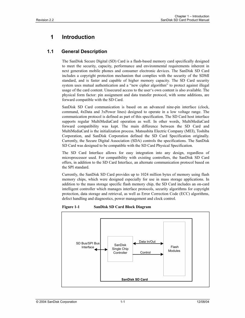
Currently, the SanDisk SD Card provides up to 1024 million bytes of memory using flash memory chips, which were designed especially for use in mass storage applications. In addition to the mass storage specific flash memory chip, the SD Card includes an on-card intelligent controller which manages interface protocols, security algorithms for copyright protection, data storage and retrieval, as well as Error Correction Code (ECC) algorithms, defect handling and diagnostics, power management and clock control.
Figure 1-1 SanDisk SD Card Block Diagram
FlashModules
SanDiskSingle ChipController Control
Data In/OutSD Bus/SPI BusInterface
SanDisk SD Card
Chapter 1 – Introduction Revision 2.2 SanDisk SD Card Product Manual
© 2004 SanDisk Corporation 1-2 12/08/04
1.2 Features
SanDisk SD Card features include: Up to 2-GB of data storage
SD-protocol compatible
Supports SPI mode
Targeted for portable and stationary applications for secured (copyrights protected) and unsecured data storage
Voltage range
Basic communication (CMD0, CMD15, CMD55, ACMD41): 2.0 to 3.6V
Other commands and memory access: 2.7 to 3.6V
Variable clock rate 0-25 MHz (default), 0-50MHz (high-speed)
Data transfer rate
Up to 50 MB/sec data transfer rate (using 4 parallel data lines)
Maximum data rate with up to 10 cards
Correction of memory-field errors
Copyrights Protection mechanism
Complies with highest security of SDMI standard
Password-protection (specific models only)
Write Protect using mechanical switch
Built-in write protection features (permanent and temporary)
Card detection (Insertion/Removal)
Application-specific commands
Comfortable erase mechanism
1.3 SD Card Standard
SanDisk SD cards are fully compatible with the SD Card Physical Layer System Specification, Version 1.10. This specification is available from the SD Card Association.
SD Association 719 San Benito St., Suite C Hollister, CA 95023 USA Phone: +1 831-636-7322 FAX: +1 831-623-2248 E-mail: [email protected] URL: http://www.sdcard.org
Chapter 1 – Introduction Revision 2.2 SanDisk SD Card Product Manual
© 2004 SanDisk Corporation 1-3 12/08/04
1.4 Functional Description
SanDisk SD cards contain a high-level, intelligent subsystem as shown in Figure 1-1. This intelligent (microprocessor) subsystem provides many capabilities not found in other types of memory cards. These capabilities include: • Host independence from details of erasing and programming flash memory • Sophisticated system for managing defects (analogous to systems found in magnetic
disk drives) • Sophisticated system for error recovery including a powerful error correction code
(ECC) • Power management for low-power operation
1.5 Independent Flash Technology
The 512-byte sector size of the SanDisk SD Card is the same as that in an IDE magnetic disk drive. To write or read a sector (or multiple sectors), the host computer software simply issues a read or write command to the SD Card. This command contains the address. The host software then waits for the command to complete. The host software does not get involved in the details of how the flash memory is erased, programmed or read. This is extremely important as flash devices are expected to get increasingly complex in the future. Because the SD Card uses an intelligent on-board controller, the host system software will not require changing as new flash memory evolves. In other words, systems that support the SD Card today will be able to access future SD cards built with new flash technology without having to update or change host software.
1.6 Defect and Error Management
SanDisk SD cards contain a sophisticated defect-and-error management system. This system is analogous to the systems found in magnetic disk drives and in many cases offers enhancements. For instance, disk drives do not typically perform a read after write to confirm the data is written correctly because of the performance penalty that would be incurred. SD cards do a read after write under margin conditions to verify that the data is written correctly. In the rare case that a bit is found to be defective, SD cards replace this bad bit with a spare bit within the sector header. If necessary, SD cards will even replace the entire sector with a spare sector. This is completely transparent to the host and does not consume any user data space.
The SD Card’s soft error rate specification is much better than the magnetic disk drive specification. In the extremely rare case a read error does occur, SD cards have innovative algorithms to recover the data. This is similar to using retries on a disk drive but is much more sophisticated. The last line of defense is to employ a powerful ECC to correct the data. If ECC is used to recover data, defective bits are replaced with spare bits to ensure they do not cause any future problems. These defect and error management systems coupled with the solid-state construction give SD cards unparalleled reliability.
Chapter 1 – Introduction Revision 2.2 SanDisk SD Card Product Manual
© 2004 SanDisk Corporation 1-4 12/08/04
1.7 Copyright Protection
A detailed description of the Copyright Protection mechanism and related security SD Card commands can be found in the SD Security Specification from the SD Association. All SD Card security-related commands operate in the data transfer mode.
As defined in the SDMI specification, data content saved in the card is already encrypted and passes transparently to and from the card. No operation is done on the data and there is no restriction to read the data at any time. Associated with every data packet (e.g., a song) that is saved in the unprotected memory, there is special data that is saved in a protected memory area for any access (Read, Write or Erase command) to or from the data in the protected area.
For an authentication procedure is done between the card and the connected device, either the LCM (PC for example) or the PD (portable device, such as SD player). After the authentication process passes, the card is ready to accept or give data from/to the connected device. While the card is in the secured mode of operation (after the authentication succeeded) the argument and the associated data that is sent to the card or read from the card are encrypted. At the end of the Read, Write or Erase operation, the card gets out automatically of its secured mode.
1.8 Endurance
SanDisk SD cards have an endurance specification for each sector of 100,000 writes typical (reading a logical sector is unlimited). This far exceeds what is typically required in almost all SD Card applications. Therefore, extremely heavy use of the card in cellular phones, personal communicators, pagers and voice recorders will use only a fraction of the total endurance over the device’s lifetime. For instance—it would take over 10 years to wear out an area on an SD Card based on a file of any size (from 512 bytes to maximum capacity) being rewritten 3 times per hour, 8 hours a day, 365 days per year.
With typical applications, the endurance limit is not of any practical concern to the vast majority of users.
1.9 Wear Leveling
Wear leveling is an intrinsic part of the erase pooling functionality of the SD Card, using NAND memory. The Wear Level command is supported as a NOP operation to maintain backward compatibility with existing software utilities.
1.10 Automatic Sleep Mode
A unique feature of the SanDisk SD Card is automatic entrance and exit from sleep mode. Upon completion of an operation, the card enters the sleep mode to conserve power if no further commands are received in less than five milliseconds (ms). The host does not have to take any action for this to occur. However, in order to achieve the lowest sleep current, the host needs to shut down its clock to the card. In most systems, the SD card is in sleep mode except when the host is accessing it, thus conserving power.
When the host is ready to access the card in sleep mode, any command issued to it will cause it to exit sleep, and respond.
Chapter 1 – Introduction Revision 2.2 SanDisk SD Card Product Manual
© 2004 SanDisk Corporation 1-5 12/08/04
1.11 Hot Insertion
Support for hot insertion will be required on the host but will be supported through the connector. Connector manufacturers will provide connectors that have power-pins long enough to be powered before contact is made with the other pins. This approach is similar to that used in PCMCIA and MMCA devices to allow for hot insertion.
1.12 SD Card—SD Bus Mode The following sections provide valuable information on the SD Card in SD Bus mode.
1.12.1 SD Card Standard Compliance
The SD Card is fully compliant with SD Card Physical Layer Standard Specification v1.10. The structure of the Card Specific Data (CSD) register is compliant with CSD Structure 1.0.
1.12.2 Negotiating Operating Conditions
The SD Card supports the operation condition verification sequence defined in the SD Card standard specifications. Should the SD Card host define an operating voltage range, which is not supported by the SD Card it will put itself in an inactive state and ignore any bus communication. The only way to get the card out of the inactive state is by powering it down and up again.
In Addition the host can explicitly send the card to the inactive state by using the GO_INACTIVE_STATE command.
1.12.3 Card Acquisition and Identification
The SD Card bus is a single master (SD Card host application) and a multi-slaves (cards) bus. The Clock and Power lines are common to all cards on the bus. During the identification process, the host accesses each card separately through its own command lines. The SD Card’s CID Register is pre-programmed with a unique card identification number, which is used during the identification procedure.
In addition, the SD Card host can read the card’s CID Register using the READ_CID command. The CID Register is programmed during the SD Card testing and formatting procedure, on the manufacturing floor. The SD Card host can only read, and not write, this register.
An internal pull-up resistor on the DAT3 line may be used for card detection (insertion/removal). The resistor can be disconnected during data transfer (using ACMD42). Additional practical card detection methods can be found in SD Physical Specification’s application notes given by the SDA.
1.12.4 Card Status The card status is separated into the following two fields: • Card Status is stored in a 32-bit status register that is sent as a data field in the card
response to host commands. The Status Register provides information about the card’s current state and completion codes for the last host command. The card status can be explicitly read (polled) with the SEND_STATUS command.
Chapter 1 – Introduction Revision 2.2 SanDisk SD Card Product Manual
© 2004 SanDisk Corporation 1-6 12/08/04
• SD Status is stored in 512 bits that are sent as a single data block after it was requested by the host using the SD_STATUS (ACMD13) command. SD_STATUS contains extended status bits that relate to BUS_WIDTH, security related bits and future specific applications.
1.12.5 Memory Array Partitioning
The basic unit of data transfer to/from the SanDisk SD Card is one byte. All data transfer operations that require a block size always define block lengths as integer multiples of bytes. Some special functions need other partition granularity. Figure 1-2 shows the Memory Array Partitioning.
For block-oriented commands, the following definition is used: • Block—A unit related to block-oriented read and write commands. Its size is the
number of bytes that are transferred when one block command is sent by the host. The size of a block is either programmable or fixed; information about allowed block sizes and the programmability is stored in the CSD Register.
The granularity of the erasable units is, in general, not the same as for the block-oriented commands: • Sector—A unit related to the erase commands. Its size is the number of blocks that are
erased in one portion. The size of a sector is fixed for each device. The information about the sector size (in blocks) is stored in the CSD Register.
For devices that include write protection, the following definition is used: • WP Group—A minimal unit that may have individual write protection. Its size is the
number of groups to be write protected by one bit. The size of a WP group is fixed for each device. The information about the size is stored in the CSD Register.
Chapter 1 – Introduction Revision 2.2 SanDisk SD Card Product Manual
© 2004 SanDisk Corporation 1-7 12/08/04
Figure 1-2 Memory Array Partitioning
Table 1-1 Memory Array Structures Summary1
Part No. Block Size
(Bytes)
Data Area + Protected size
(Blocks)
Protected Area2 size (Blocks)
User Area (Blocks0
SDSDH-2048 512 4,011,520 40,448 3,971,072
SDSDJ-2048 512 4,011,520 40,448 3,971,072
SDSDX3-1024 512 2,004,480 20,480 1,984,000
SDSDH-1024 512 2,004,480 20,480 1,984,000
SDSDJ-1024 512 2,004,480 20,480 1,984,000
SDSDH-512 512 1,001,216 10,240 990,976
SDSDJ-512 512 1,001,216 10,240 990,976
SDSDH-256 512 499,456 5,376 494,080
SDSDJ-256 512 499,456 5,376 494,080
SDSDJ-128 512 248,640 2,624 246,016
SDSDJ-64 512 123,232 1,376 121,856
1 All measurements are in units per card. 2 The part of the card that relates to the secured copyright management and has separate DOS partitioning including sectors and blocks. The card write-protection mechanism does not affect this area.
SanDisk SD Memory Card
Sector 1
Sector 2
Sector 3
Sector n
WP Group 0
Block 0
Block 1
Block 2
Block n
WP Group 1
WP Group 2
Sector 1
Sector n
Protected Area (Copyright Protection)
Block 0
Block 1
Block 2
Block n
Chapter 1 – Introduction Revision 2.2 SanDisk SD Card Product Manual
© 2004 SanDisk Corporation 1-8 12/08/04
Part No. Block Size
(Bytes)
Data Area + Protected size
(Blocks)
Protected Area2 size (Blocks)
User Area (Blocks0
SDSDJ-32 512 60,512 736 59,776
SDSDB-16 512 29,152 352 28,800
1.12.6 Read/Write Operations
The SD Card supports two read/write modes as shown in Figure 1-3 and defined in Table 1-2.
Figure 1-3 Data Transfer Formats
Table 1-2 Mode Definitions
Mode Description
Single Block In this mode the host reads or writes one data block in a pre-specified length. The data block transmission is protected with 16-bit CRC that is generated by the sending unit and checked by the receiving unit.
The block length for read operations is limited by the device sector size (512 bytes) but can be as small as a single byte. Misalignment is not allowed. Every data block must be contained in a single physical sector.
The block length for write operations must be identical to the sector size and the start address aligned to a sector boundary.
Multiple Block This mode is similar to the single block mode, except for the host can read/write multiple data blocks (all have the same length) that are stored or retrieved from contiguous memory addresses starting at the address specified in the command. The operation is terminated with a stop transmission command.
Misalignment and block length restrictions apply to multiple blocks and are identical to the single block read/write operations.
1.12.7 Data Transfer Rate
The SD Card can be operated using either a single data line (DAT0) or four data lines (DAT0-DAT3) for data transfer. The maximum data transfer rate for a single data line is 50-Mb per second, and 200-Mb (25 MB) per second using four data lines.
Multiple Block Mode
MemorySectors
MemorySectors
MemorySectors
MemorySectors
MemorySectors
MemorySectors
MemorySectors
MemorySectors
MemorySectors
MemorySectors
MemorySectors
MemorySectors
MemorySectors
MemorySectors
Start Address(Write)
Start Address(Read/Write)
Start Address(Read)
Write
Start Address Stop Start
Read
Stop
Single Block Mode Misalignment Error
Chapter 1 – Introduction Revision 2.2 SanDisk SD Card Product Manual
© 2004 SanDisk Corporation 1-9 12/08/04
1.12.8 Data Protection in the Flash Card
Every sector is protected with an error correction code (ECC). The ECC is generated (in the memory card) when the sectors are written and validated when the data is read. If defects are found, the data is corrected prior to transmission to the host.
1.12.9 Write Protection
Two-card level write-protection options are available: permanent and temporary. Both can be set using the PROGRAM_CSD command (refer to CSD Programming). The permanent write-protect bit, once set, cannot be cleared. This feature is implemented in the SD Card controller firmware and not with a physical OTP cell.
Use the Write Protect (WP) Switch located on the card’s side edge to prevent the host from writing to or erasing data on the card. The WP switch does not have any influence on the internal Permanent or Temporary WP bits in the CSD Register.
1.12.10 Copy Bit
The copy bit can be used to mark an SD Card content as an original or a copy. The copy bit of the card is programmed as a copy when testing and formatting are performed during manufacturing. When set, the copy bit in the CSD Register is a copy and cannot be cleared.
The card is available with the copy-bit set or cleared. If the bit is set, it indicates that the card is a master. This feature is implemented in the card’s controller firmware and not with a physical OTP cell.
1.12.11 CSD Register
All SD Card configuration information is stored in the CSD Register. The MSB bytes of the register contain manufacturer data and the two least significant bytes contain the host-controlled data: the card copy/write protection, and the user file format.
The host can read the CSD Register and alter the host-controlled data bytes using the SEND_CSD and PROGRAM_CSD commands.
1.13 SPI Mode The SPI mode is a secondary communication protocol for SD cards. This mode is a subset of the SD Protocol, designed to communicate with an SPI channel, commonly found in Motorola and other vendors’ microcontrollers.
Table 1-3 SPI Mode
Function Description
Negotiating Operating Conditions The operating condition negotiation function of the SD Card bus is supported differently in SPI mode by using the READ_OCR (CMD58) command. The host works within the valid voltage range (2.7 to 3.6 v) of the card or put the card in inactive state by sending a GO_INACTIVE command to the card.
Card Acquisition and Identification The host must know the number of cards currently connected on the bus. Specific card selection is done via the CS signal (CD/DAT3). The internal pull-up resistor on the CD/DAT3 line may be used for card detection (insertion/removal). Additional practical card detection methods can be found in SD Physical Specification’s Application Notes given by the SDA.
Chapter 1 – Introduction Revision 2.2 SanDisk SD Card Product Manual
© 2004 SanDisk Corporation 1-10 12/08/04
Function Description
Card Status In SPI mode, only 16 bits containing errors relevant to SPI mode can be read out of the 32-bit Status Register. The SD_STATUS can be read using ACMD13, the same as in SD mode.
Memory Array Partitioning Memory partitioning in SPI mode is equivalent to SD mode. All read and write commands are byte addressable.
Read/Write Operations In SPI mode, single and multiple block data transfers are supported.
Data Transfer Rate Same as in SD mode.
Data Protection in the SD Card Same as in SD mode.
Erase Same as in SD mode.
Write Protection Same as in SD mode.
Copyright Protection Same as in SD mode.
Chapter 2 – Product Specifications Revision 2.2 SanDisk SD Card Product Manual
© 2004 SanDisk Corporation 2-1 12/08/04
2 Product Specifications
2.1 Overview In this section, all values are defined at an ambient temperature and nominal supply voltage unless otherwise stated.
2.2 System Environmental Specifications Table 2-1 defines the environmental specifications for the SanDisk SD Card.
Table 2-1 Environmental Specification Summary
Operating -25° C to 85° C Temperature
Non-operating -40° C to 85° C
Operating 25% to 95%, non condensing Humidity
Non-operating 25% to 95%, non condensing
Contact Pads +/- 4kV, Human body model according to ANSI EOS/ESD-S5.1-1998
ESD Protection
Non Contact Pad Area +/- 8kV (coupling plane discharge) +/- 15kV (air discharge) Human body model per IEC61000-4-2.
2.3 Reliability and Durability
Table 2-2 Reliability and Durability Specifications
Durability 10,000 mating cycles
Bending 10N
Torque 0.15N.m or ±2.5 deg.
Drop Test 1.5m free fall
UV Light Exposure UV: 254nm, 15Ws/cm2 according to ISO 7816-1
Visual Inspection/Shape and Form No warpage; no mold skin; complete form; no cavities; surface smoothness ≤ -0.1 mm/cm2 within contour; no cracks; no pollution (oil, dust, etc.)
Minimum Moving Force of WP Switch 40 gf (ensures that the WP switch will not slide while it is inserted in the connector).
WP Switch Cycles Minimum 1,000 Cycles @ slide force 0.4N to 5N
Chapter 2 – Product Specifications Revision 2.2 SanDisk SD Card Product Manual
© 2004 SanDisk Corporation 2-2 12/08/04
2.4 Typical Card Power Requirements
Table 2-3 Card Power Requirements (Ta=25°[email protected])
VDD (ripple: max, 60mV peak-to-peak) 2.7 V – 3.6 V
Value Measurement Average
Sleep 250 uA Max
Read 65 mA Max
Write 75 mA Max
2.5 System Performance All performance values for the SD Card in Table 2-4 are under the following conditions: • Voltage range 2.7 V to 3.6 V • Temperature -25° C to 85° C • Independent of the SD Card clock frequency
Table 2-4 System Performance
Timing Typical Maximum
Block Read Access Time 0.5 ms 100 ms
Block Write Access Time 0.5 ms 250 ms
CMD1 to Ready after Power-up
50 ms 500 ms
Sleep to Ready 1 ms 2 ms
2.6 System Reliability and Maintenance Table 2-5 Reliability and Maintenance Specifications
MTBF >1,000,000 hours
Preventative Maintenance None
Data Reliability <1 non-recoverable error in 1014 bits read
Endurance 100,000 write and erase cycles (typical)
Chapter 2 – Product Specifications Revision 2.2 SanDisk SD Card Product Manual
© 2004 SanDisk Corporation 2-3 12/08/04
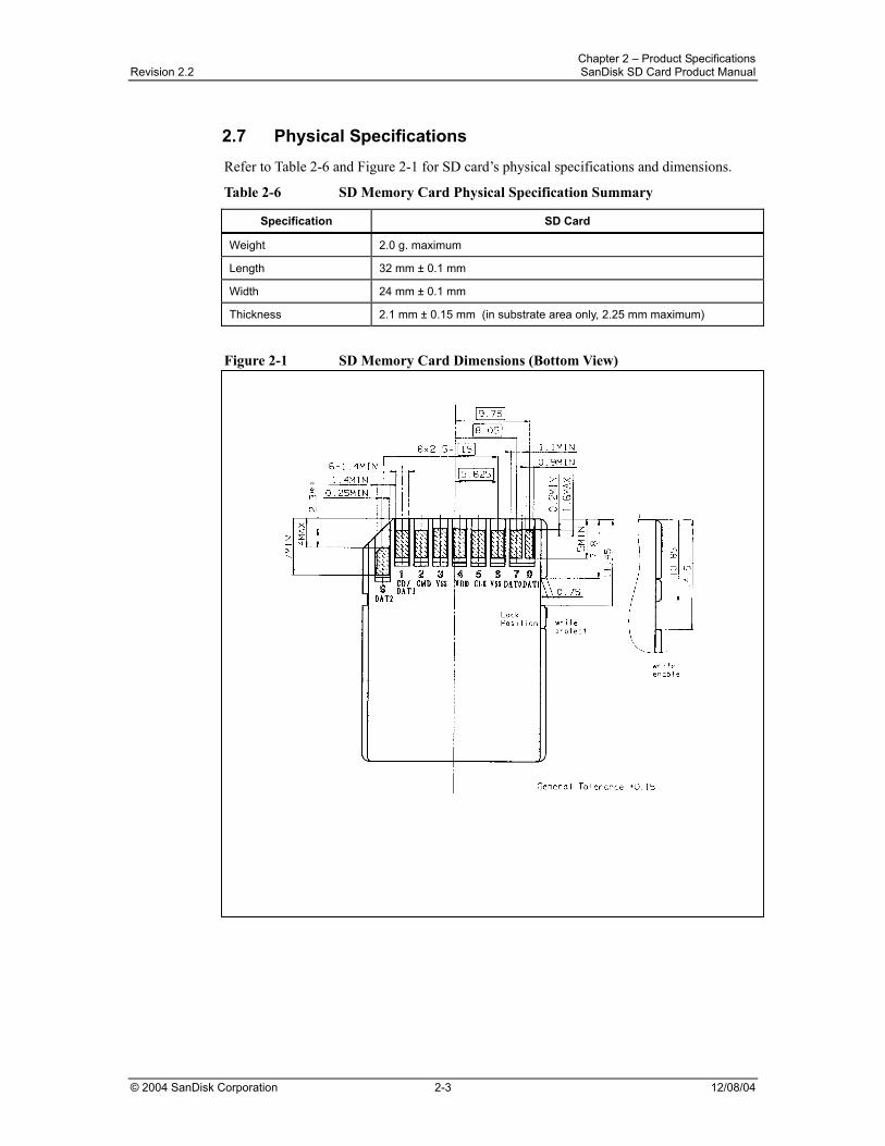
2.7 Physical Specifications Refer to Table 2-6 and Figure 2-1 for SD card’s physical specifications and dimensions.
Table 2-6 SD Memory Card Physical Specification Summary
Specification SD Card
Weight 2.0 g. maximum
Length 32 mm ± 0.1 mm
Width 24 mm ± 0.1 mm
Thickness 2.1 mm ± 0.15 mm (in substrate area only, 2.25 mm maximum)
Figure 2-1 SD Memory Card Dimensions (Bottom View)
Chapter 2 – Product Specifications Revision 2.2 SanDisk SD Card Product Manual
© 2004 SanDisk Corporation 2-4 12/08/04
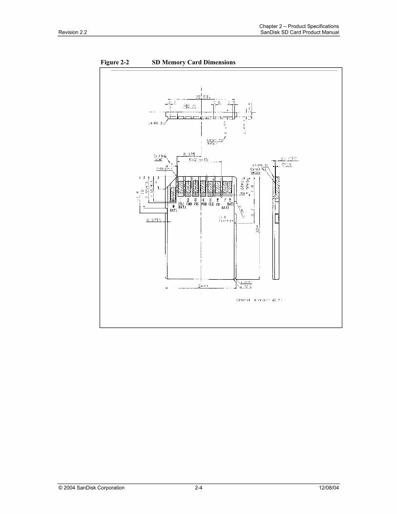
Figure 2-2 SD Memory Card Dimensions
Chapter 2 – Product Specifications Revision 2.2 SanDisk SD Card Product Manual
© 2004 SanDisk Corporation 2-5 12/08/04
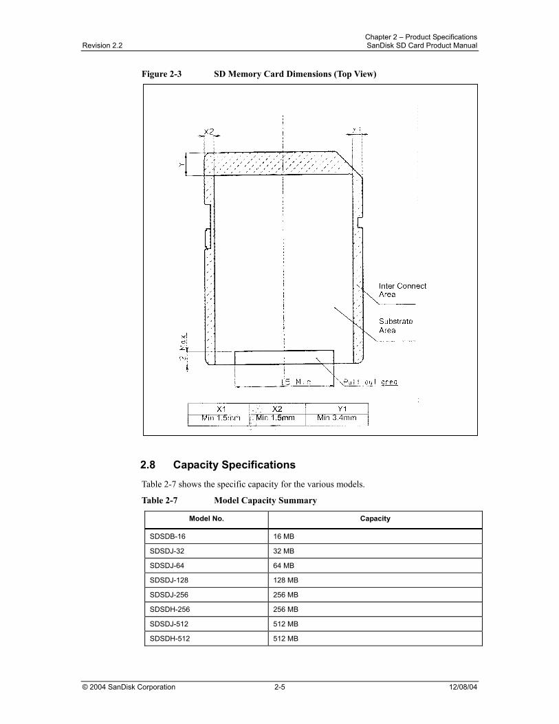
Figure 2-3 SD Memory Card Dimensions (Top View)
2.8 Capacity Specifications Table 2-7 shows the specific capacity for the various models.
Table 2-7 Model Capacity Summary
Model No. Capacity
SDSDB-16 16 MB
SDSDJ-32 32 MB
SDSDJ-64 64 MB
SDSDJ-128 128 MB
SDSDJ-256 256 MB
SDSDH-256 256 MB
SDSDJ-512 512 MB
SDSDH-512 512 MB
Chapter 2 – Product Specifications Revision 2.2 SanDisk SD Card Product Manual
© 2004 SanDisk Corporation 2-6 12/08/04
Model No. Capacity
SDSDJ-1024 1024 MB
SDSDH-1024 1024 MB
SDSDX3-1024 1024 MB
SDSDJ-2048 2048 MB
SDSDH-2048 2048 MB
Chapter 3 – SD Card Interface Description Revision 2.2 SD Card Product Manual
© 2004 SanDisk Corporation 3-1 12/08/04
3 SD Card Interface Description
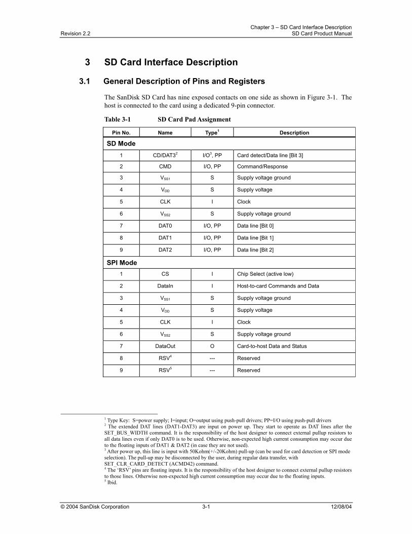
3.1 General Description of Pins and Registers
The SanDisk SD Card has nine exposed contacts on one side as shown in Figure 3-1. The host is connected to the card using a dedicated 9-pin connector.
Table 3-1 SD Card Pad Assignment
Pin No. Name Type1 Description
SD Mode 1 CD/DAT32 I/O3, PP Card detect/Data line [Bit 3]
2 CMD I/O, PP Command/Response
3 VSS1 S Supply voltage ground
4 VDD S Supply voltage
5 CLK I Clock
6 VSS2 S Supply voltage ground
7 DAT0 I/O, PP Data line [Bit 0]
8 DAT1 I/O, PP Data line [Bit 1]
9 DAT2 I/O, PP Data line [Bit 2]
SPI Mode 1 CS I Chip Select (active low)
2 DataIn I Host-to-card Commands and Data
3 VSS1 S Supply voltage ground
4 VDD S Supply voltage
5 CLK I Clock
6 VSS2 S Supply voltage ground
7 DataOut O Card-to-host Data and Status
8 RSV4 --- Reserved
9 RSV5 --- Reserved
1 Type Key: S=power supply; I=input; O=output using push-pull drivers; PP=I/O using push-pull drivers 2 The extended DAT lines (DAT1-DAT3) are input on power up. They start to operate as DAT lines after the SET_BUS_WIDTH command. It is the responsibility of the host designer to connect external pullup resistors to all data lines even if only DAT0 is to be used. Otherwise, non-expected high current consumption may occur due to the floating inputs of DAT1 & DAT2 (in case they are not used). 3 After power up, this line is input with 50Kohm(+/-20Kohm) pull-up (can be used for card detection or SPI mode selection). The pull-up may be disconnected by the user, during regular data transfer, with SET_CLR_CARD_DETECT (ACMD42) command. 4 The ‘RSV’ pins are floating inputs. It is the responsibility of the host designer to connect external pullup resistors to those lines. Otherwise non-expected high current consumption may occur due to the floating inputs. 5 Ibid.
Chapter 3 – SD Card Interface Description Revision 2.2 SD Card Product Manual
© 2004 SanDisk Corporation 3-2 12/08/04
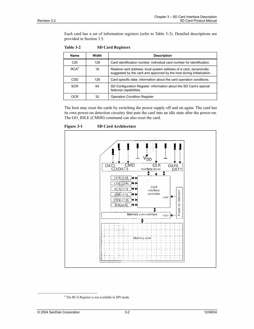
Each card has a set of information registers (refer to Table 3-3). Detailed descriptions are provided in Section 3.5.
Table 3-2 SD Card Registers
Name Width Description
CID 128 Card identification number: individual card number for identification.
RCA6 16 Relative card address: local system address of a card, dynamically suggested by the card and approved by the host during initialization.
CSD 128 Card specific data: information about the card operation conditions.
SCR 64 SD Configuration Register: information about the SD Card’s special features capabilities.
OCR 32 Operation Condition Register
The host may reset the cards by switching the power supply off and on again. The card has its own power-on detection circuitry that puts the card into an idle state after the power-on. The GO_IDLE (CMD0) command can also reset the card.
Figure 3-1 SD Card Architecture
6 The RCA Register is not available in SPI mode.
Chapter 3 – SD Card Interface Description Revision 2.2 SD Card Product Manual
© 2004 SanDisk Corporation 3-3 12/08/04
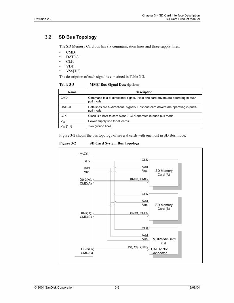
3.2 SD Bus Topology
The SD Memory Card bus has six communication lines and three supply lines. • CMD • DAT0-3 • CLK • VDD • VSS[1:2] The description of each signal is contained in Table 3-3.
Table 3-3 MMC Bus Signal Descriptions
Name Description
CMD Command is a bi-directional signal. Host and card drivers are operating in push-pull mode.
DAT0-3 Data lines are bi-directional signals. Host and card drivers are operating in push-pull mode.
CLK Clock is a host to card signal. CLK operates in push-pull mode.
VDD Power supply line for all cards.
VSS [1:2] Two ground lines.
Figure 3-2 shows the bus topology of several cards with one host in SD Bus mode.
Figure 3-2 SD Card System Bus Topology
SD MemoryCard (A)
CLK
VddVss
D0-D3, CMD
SD MemoryCard (B)
CLK
VddVss
D0-D3, CMD
MultiMediaCard(C)
CLK
VddVss
D0, CS, CMD
CLK
VddVss
D0-3(A),CMD(A)
D0-3(B),CMD(B)
D0-3(C)CMD(C)
HOST
D1&D2 NotConnected
Chapter 3 – SD Card Interface Description Revision 2.2 SD Card Product Manual
© 2004 SanDisk Corporation 3-4 12/08/04
During the initialization process, commands are sent to each card individually, allowing the application to detect the cards and assign logical addresses to the physical slots. Data is always sent to each card individually. However, to simplify the handling of the card stack, after initialization, all commands may be sent concurrently to all cards. Addressing information is provided in the command packet.
The SD bus allows dynamic configuration of the number of data lines. After power-up, by default, the SD Card will use only DAT0 for data transfer. After initialization, the host can change the bus width (number of active data lines). This feature allows and easy trade off between hardware cost and system performance.
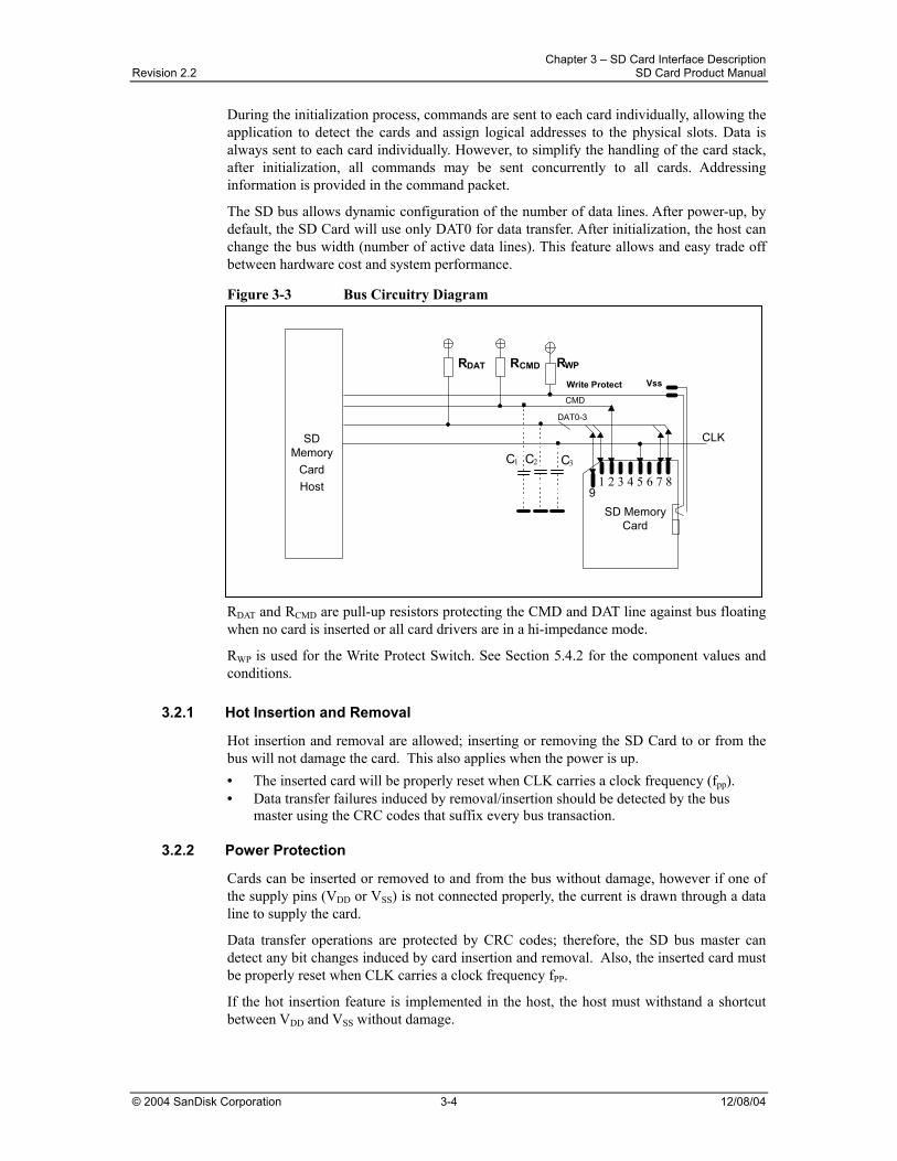
Figure 3-3 Bus Circuitry Diagram
RDAT and RCMD are pull-up resistors protecting the CMD and DAT line against bus floating when no card is inserted or all card drivers are in a hi-impedance mode.
RWP is used for the Write Protect Switch. See Section 5.4.2 for the component values and conditions.
3.2.1 Hot Insertion and Removal
Hot insertion and removal are allowed; inserting or removing the SD Card to or from the bus will not damage the card. This also applies when the power is up. • The inserted card will be properly reset when CLK carries a clock frequency (fpp). • Data transfer failures induced by removal/insertion should be detected by the bus
master using the CRC codes that suffix every bus transaction.
3.2.2 Power Protection
Cards can be inserted or removed to and from the bus without damage, however if one of the supply pins (VDD or VSS) is not connected properly, the current is drawn through a data line to supply the card.
Data transfer operations are protected by CRC codes; therefore, the SD bus master can detect any bit changes induced by card insertion and removal. Also, the inserted card must be properly reset when CLK carries a clock frequency fPP.
If the hot insertion feature is implemented in the host, the host must withstand a shortcut between VDD and VSS without damage.
CMD
CLK
DAT0-3
SDMemory
CardHost 1 2 3 4 5 6 7 8
SD MemoryCard
RDAT RCMD
C1 C2 C3
9
RWP
VssWrite Protect
Chapter 3 – SD Card Interface Description Revision 2.2 SD Card Product Manual
© 2004 SanDisk Corporation 3-5 12/08/04
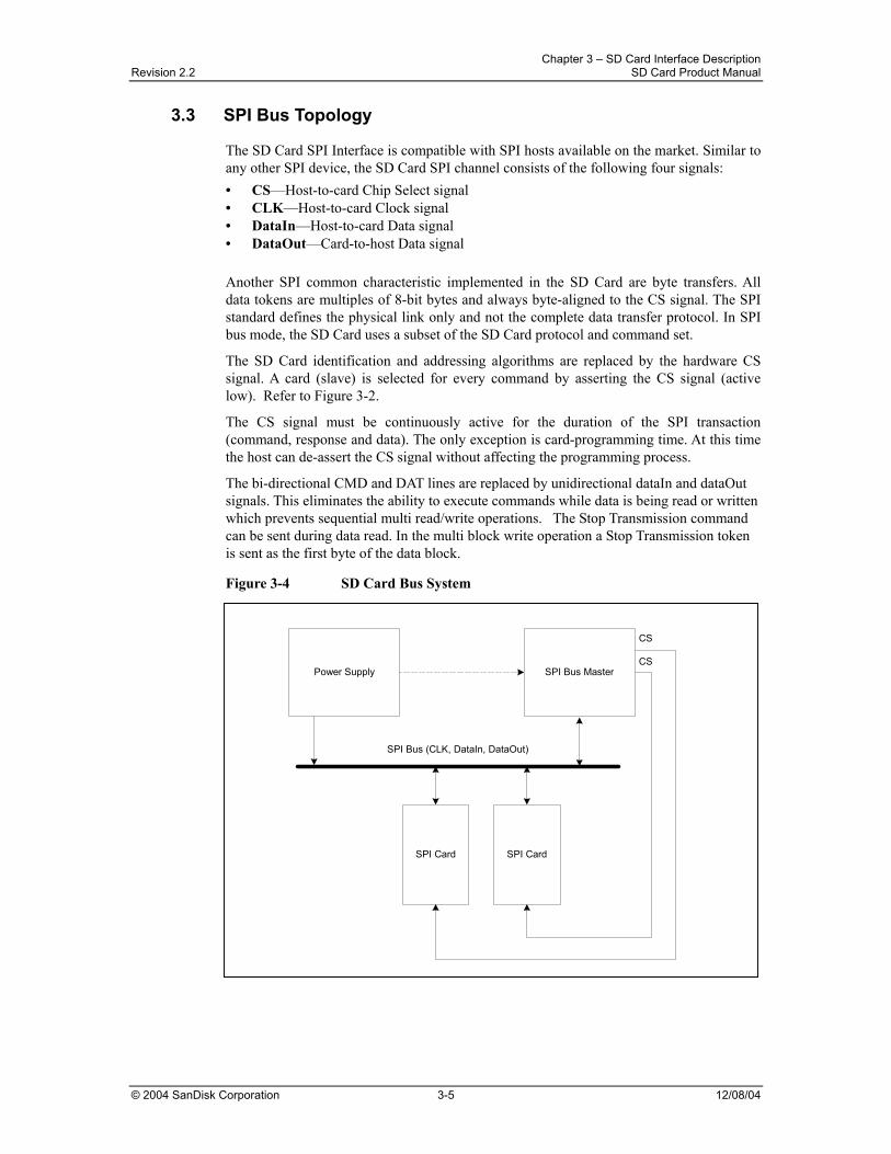
3.3 SPI Bus Topology
The SD Card SPI Interface is compatible with SPI hosts available on the market. Similar to any other SPI device, the SD Card SPI channel consists of the following four signals: • CS—Host-to-card Chip Select signal • CLK—Host-to-card Clock signal • DataIn—Host-to-card Data signal • DataOut—Card-to-host Data signal Another SPI common characteristic implemented in the SD Card are byte transfers. All data tokens are multiples of 8-bit bytes and always byte-aligned to the CS signal. The SPI standard defines the physical link only and not the complete data transfer protocol. In SPI bus mode, the SD Card uses a subset of the SD Card protocol and command set.
The SD Card identification and addressing algorithms are replaced by the hardware CS signal. A card (slave) is selected for every command by asserting the CS signal (active low). Refer to Figure 3-2.
The CS signal must be continuously active for the duration of the SPI transaction (command, response and data). The only exception is card-programming time. At this time the host can de-assert the CS signal without affecting the programming process.
The bi-directional CMD and DAT lines are replaced by unidirectional dataIn and dataOut signals. This eliminates the ability to execute commands while data is being read or written which prevents sequential multi read/write operations. The Stop Transmission command can be sent during data read. In the multi block write operation a Stop Transmission token is sent as the first byte of the data block.
Figure 3-4 SD Card Bus System
SPI Bus Master
SPI Card SPI Card
Power Supply
SPI Bus (CLK, DataIn, DataOut)
CS
CS
Chapter 3 – SD Card Interface Description Revision 2.2 SD Card Product Manual
© 2004 SanDisk Corporation 3-6 12/08/04
3.3.1 Power Protection
Same as in SD Card Bus Mode.
3.4 Electrical Interface
The following sections provide valuable information about the electrical interface.
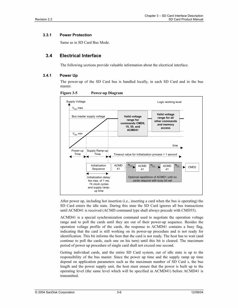
3.4.1 Power Up The power-up of the SD Card bus is handled locally, in each SD Card and in the bus master.
Figure 3-5 Power-up Diagram
After power up, including hot insertion (i.e., inserting a card when the bus is operating) the SD Card enters the idle state. During this state the SD Card ignores all bus transactions until ACMD41 is received (ACMD command type shall always precede with CMD55).
ACMD41 is a special synchronization command used to negotiate the operation voltage range and to poll the cards until they are out of their power-up sequence. Besides the operation voltage profile of the cards, the response to ACMD41 contains a busy flag, indicating that the card is still working on its power-up procedure and is not ready for identification. This bit informs the host that the card is not ready. The host has to wait (and continue to poll the cards, each one on his turn) until this bit is cleared. The maximum period of power up procedure of single card shall not exceed one second.
Getting individual cards, and the entire SD Card system, out of idle state is up to the responsibility of the bus master. Since the power up time and the supply ramp up time depend on application parameters such as the maximum number of SD Card s, the bus length and the power supply unit, the host must ensure that the power is built up to the operating level (the same level which will be specified in ACMD41) before ACMD41 is transmitted.
Power-upTime
Supply Ramp-upTime Timeout value for initialization process = 1 second
time
Supply Voltage
VDD max
Bus master supply voltage
Logic working level
InitializationSequence
ACMD41
Initialization delay:the max. of 1 ms,74 clock cycles
and supply ramp-up time
Optional repetitions of ACMD1 until nocards respond with busy bit set
ACMD41
ACMD41
CMD2
VDD min
NCC NCC NCC
Valid voltagerange for all
other commandsand memory
access
Valid voltagerange for
commands CMD0,15, 55, andACMD41
Chapter 3 – SD Card Interface Description Revision 2.2 SD Card Product Manual
© 2004 SanDisk Corporation 3-7 12/08/04
After power up, the host starts the clock and sends the initializing sequence on the CMD line. This sequence is a contiguous stream of logical ‘1’s. The sequence length is the maximum of 1msec, 74 clocks or the supply-ramp-up-time; the additional 10 clocks (over the 64 clocks after what the card should be ready for communication) is provided to eliminate power-up synchronization problems.
Every bus master shall have the capability to implement ACMD41 and CMD1. CMD1 will be used to ask MultiMediaCards to send their operation conditions. In any case the ACMD41 or the CMD1 shall be send separately to each card accessing it through its own CMD line.
3.4.2 Bus Operating Conditions
SPI Mode bus operating conditions are identical to SD Card mode bus operating conditions. Table 3-4 lists the power supply voltages. The CS (chip select) signal timing is identical to the input signal timing (see Figure 3-8).
Table 3-4 Bus Operating Conditions Summary
Parameter Symbol Min Max Unit RemarkGeneral Peak voltage on all lines --- -0.3 VDD + 0.3 V
All Inputs
Input Leakage Current --- -10 10 uA
All Outputs
Output Leakage Current --- -10 10 uA
Power Supply Voltage7
Supply Voltage VDD 2.0 3.6 V CMD0, 15, 55, ACMD41 commands
VDD 2.7 3.6 V Except CMD0, 15, 55, ACMD41 commands
Supply voltage differentials (VSS1, VSS2)
--- -0.3 0.3 V
Power-up Time --- --- 250 mS From 0 V to VDD min.
3.4.3 Bus Signal Line Load
The total capacitance, CL, of the clock line in the SD Card bus is the sum of the bus-master capacitance (CHOST), the bus capacitance (CBUS) itself and the capacitance (CCARD) of each card connected to this line:
CL = CHOST + CBUS + N*CCARD
Where N is the number of connected cards. Requiring the sum of the host and bus capacitances not to exceed 30 pF for up to 10 cards, and 40 pF for up to 30 cards, the values in Table 3-4 must not be exceeded.
7 The current consumption of any card during the power-up procedure must not exceed 10 mA.
Chapter 3 – SD Card Interface Description Revision 2.2 SD Card Product Manual
© 2004 SanDisk Corporation 3-8 12/08/04
Table 3-5 Host and Bus Capacities8
Parameter Symbol Min. Max. Unit RemarkPull-up resistance RCMD,
RDAT
10 100 kΩ Prevents bus floating
Bus signal line capacitance CL --- 250 pF fPP < 5 MHz, 21 cards
Bus signal line capacitance CL --- 100 pF
Signal card capacitance CCARD --- 10 pF
fPP < 20 MHz, 7 cards
Max. signal line inductance --- --- 16 nH fPP <20 MHz Pull-up resistance inside card (pin 1) RDAT3 10 90 kΩ May be used for card
detection
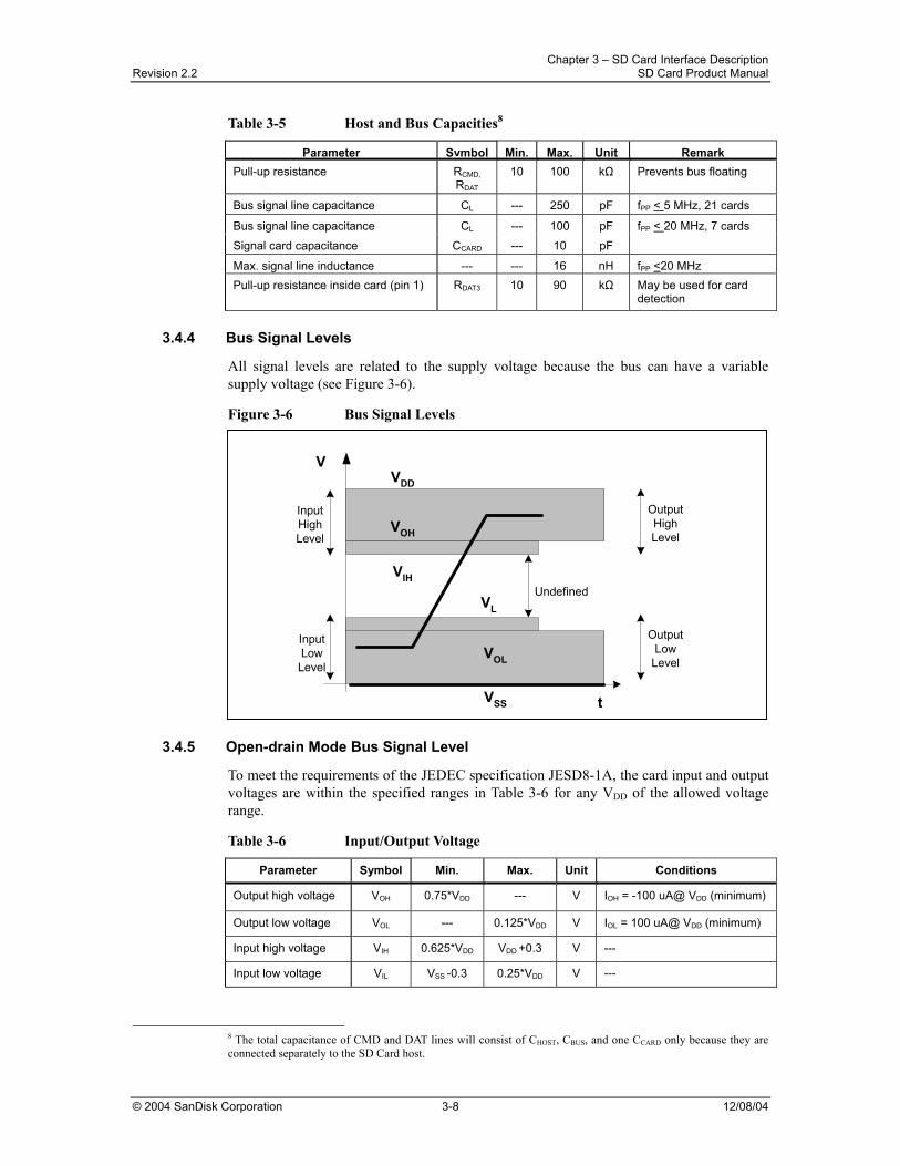
3.4.4 Bus Signal Levels
All signal levels are related to the supply voltage because the bus can have a variable supply voltage (see Figure 3-6).
Figure 3-6 Bus Signal Levels
3.4.5 Open-drain Mode Bus Signal Level
To meet the requirements of the JEDEC specification JESD8-1A, the card input and output voltages are within the specified ranges in Table 3-6 for any VDD of the allowed voltage range.
Table 3-6 Input/Output Voltage
Parameter Symbol Min. Max. Unit Conditions
Output high voltage VOH 0.75*VDD --- V IOH = -100 uA@ VDD (minimum)
Output low voltage VOL --- 0.125*VDD V IOL = 100 uA@ VDD (minimum)
Input high voltage VIH 0.625*VDD VDD +0.3 V ---
Input low voltage VIL VSS -0.3 0.25*VDD V ---
8 The total capacitance of CMD and DAT lines will consist of CHOST, CBUS, and one CCARD only because they are connected separately to the SD Card host.
InputLow
Level
InputHighLevel
OutputHighLevel
OutputLow
Level
Undefined
VDD
VOH
VIH
VL
VOL
VSS t
V
Chapter 3 – SD Card Interface Description Revision 2.2 SD Card Product Manual
© 2004 SanDisk Corporation 3-9 12/08/04
3.4.6 Bus Timing (default)
Default dataIn/dataOut timing is illustrated in Figure 3-7; bus timing parameter values are shown in Table 3-7.
Figure 3-7 Data In/Out Referenced to Clock Timing (default)
Table 3-7 Bus Timing Parameter Values (default)
Parameter Symbol Min Max Unit Remark
Clock (CLK) – all values referred to min. VIH and max. VIL
Clock Freq. Data Transfer Mode fPP 0 25 MHz CL < 100 pF (7 cards)
Clock Freq. Identification Mode9 fOD 010/100
400 kHz CL < 250 pF (21 cards)
Clock Low Time tWL 10 --- ns CL < 100 pF (7 cards)
Clock High Time tWH 10 --- ns CL < 100 pF (7 cards)
Clock Rise Time tTLH --- 10 ns CL < 100 pF (10 cards)
Clock Fall Time tTHL --- 10 ns CL < 100 pF (7 cards)
Clock Low Time tWL 50 --- ns CL < 250 pF (21 cards)
Clock High Time tWH 50 --- ns CL < 250 pF (21 cards)
Clock Rise Time tTLH --- 50 ns CL < 250 pF (21 cards)
Clock Fall Time tTHL --- 50 ns CL < 250 pF (21 cards)
Inputs CMD, DAT – referenced to CLK
Input setup time tISU 5 --- ns CL < 25 pF (1 card)
Input hold time tIH 5 --- ns CL < 25 pF (1 card)
Outputs CMD, DAT – referenced to CLK
9 Low frequency required for MMC compatibility. 10 0 Hz stops clock—given min. freq. range is for cases in which a continuous clock is required.
Chapter 3 – SD Card Interface Description Revision 2.2 SD Card Product Manual
© 2004 SanDisk Corporation 3-10 12/08/04
Parameter Symbol Min Max Unit Remark
Clock (CLK) – all values referred to min. VIH and max. VIL
Output delay time during Data Transfer mode
tOSU 0 14 ns CL < 25 pF (1 card)
Output delay time during Identification mode
tODLY 0 50 ns CL < 25 pF (1 card)
3.4.7 Bus Timing (high-speed mode)
High-speed mode dataIn/dataOut timing is illustrated in Figure 3-8; bus timing parameter values are shown in Table 3-8.
Figure 3-8 Data In/Out Referenced to Clock Timing (high-speed)
Table 3-8 Bus Timing Parameter Values (high-speed)
Parameter Symbol Min Max Unit Remark
Clock (CLK) – all values referred to min. VIH and max. VIL
Clock Freq. Data Transfer Mode fPP 0 50 MHz
Clock Low Time tWL 7 --- ns
Clock High Time tWH 7 --- ns
Clock Rise Time tTLH --- 3 ns
Clock Fall Time tTHL --- 3 ns
Inputs CMD, DAT – referenced to CLK
Input setup time tISU 6 --- ns
Input hold time tIH 2 --- ns
Outputs CMD, DAT – referenced to CLK
Output delay time during Data Transfer mode
tODLY --- 14 ns
Chapter 3 – SD Card Interface Description Revision 2.2 SD Card Product Manual
© 2004 SanDisk Corporation 3-11 12/08/04
Parameter Symbol Min Max Unit Remark
Clock (CLK) – all values referred to min. VIH and max. VIL
Output hold time tOH 2.5 --- ns
Total system capacitance for each line11
CL --- 40 pF
3.5 SD Card Registers
There is a set of six registers within the card interface. The OCR, CID, CSD, and SCR registers carry the card configuration information. The RCA Register holds the card-relative communication address for the current session. The card status and SD status registers hold the communication protocol related status of the card.
3.5.1 Operating Conditions Register
The 32-bit Operation Conditions Register (OCR) stores the VDD voltage profile of the SanDisk SD Card. The card is capable of executing the voltage recognition procedure (CMD1) with any standard SD Card host using operating voltages from 2 to 3.6 V.
Accessing the data in the memory array, however, requires 2.7 to 3.6 V. The OCR shows the voltage range in which the card data can be accessed. The structure of the OCR Register is described in Table 3-9.
Table 3-9 Operating Conditions Register
OCR Bit VDD Voltage Window OCR Bit VDD Voltage Window
0-3 Reserved 15 2.7 to 2.8
4 1.6 to 1.7 16 2.8 to 2.9
5 1.7 to 1.8 17 2.9 to 3.0
6 1.8 to 1.9 18 3.0 to 3.1
7 1.9 to 2.0 19 3.1 to 3.2
8 2.0 to 2.1 20 3.2 to 3.3
9 2.1 to 2.2 21 3.3 to 3.4
10 2.2 to 2.3 22 3.4 to 3.5
11 2.3 to 2.4 23 3.5 to 3.6
12 2.4 to 2.5 24-30 Reserved
13 2.5 to 2.6 31 Card power-up status bit
14 2.6 to 2.7
11 In order to satisfy severe timing, the host will drive only one card.
Chapter 3 – SD Card Interface Description Revision 2.2 SD Card Product Manual
© 2004 SanDisk Corporation 3-12 12/08/04
3.5.2 Card Identification Register
The Card Identification Register (CID)12 is 16 bytes long and contains a unique card identification number as shown in Table 3-10. It is programmed during card manufacturing and cannot be changed by SD Card hosts.
Table 3-10 CID Register Definitions
Name Type Width CID-Slice CID Value Comments
Manufacturer ID (MID) Binary 8 [127:120] 0x03 Manufacturer IDs are controlled and assigned by the SD Card Association
OEM/Application ID (OID) ASCII 16 [119:104] SD ASCII Code 0x53, 0x44
Identifies the card OEM and/or the card contents. The OID is assigned by the 3C.13
Product Name (PNM) ASCII 40 [103:64] SD02G SD01G SD512 SD256 SD128 SD64 SD32 SD16
Five ASCII characters long
Product Revision14 BCD 8 [63:56] Product Revision xx
Two binary-coded decimal digits
Serial Number (PSN) Binary 32 [55:24] Product Serial Number
32-bit unsigned integer
Reserved --- 4 [23:20] --- ---
Manufacture Date Code (MDT)
BCD 12 [19:8] Manufacture date (for ex. April 2001= 0x014)
Manufacturing date—yym (offset from 2000)
CRC7 checksum (CRC) Binary 7 [7:1] CRC7* Calculated
Not used, always “1” --- 1 [0.0] --- ---
*The CRC checksum is computed by using the following formula:
CRC Calculation: G(x)=x7+3+1
M(x)=(MID-MSB)*x119+…+(CIN-LSB)*x0
CRC[6…0]=Remainder[(M(x)*x7)/G(x)]
12 The CID Register in the SD Card has a different structure than in the MultiMediaCard. 13 3C represents the three SDA founding companies: Toshiba, SanDisk, and MEI. 14 The product revision is composed of two binary-coded decimal (BCD) digits (4 bits ea.) representing and “n.m” revision number. The “n” is the most significant nibble and the “m” is the least significant nibble. Example: the PRV binary value filed for product revision (6.2) would be “01100010”.
Chapter 3 – SD Card Interface Description Revision 2.2 SD Card Product Manual
© 2004 SanDisk Corporation 3-13 12/08/04
3.5.3 Card Specific Data Register
The Card Specific Data (CSD) Register configuration information is required to access the card data.
In Table 3-11, the Cell Type column defines the CSD field as read-only (R), one-time programmable (R/W) or erasable (R/W/E). The values are presented in “real world” units for each field and coded according to the CSD structure.
Table 3-11 CSD Register Fields
Field Width Cell Type
CSD Slice
CSD Value CSD Code Description
CSD_ STRUCTURE
2 R [127: 126]
1.0 0 CSD structure
--- 6 R [125: 120]
--- 000000b Reserved
TAAC
8 R [119: 112]
1.5 msec 00100110 Data read access time-1
NSAC 8 R [111: 104]
0 00000000b Data read access time-2 in CLK cycles (NSAC*100)
Default 25MHz 0110010 TRANS_ SPEED
8 R [103:96]
High-speed 50MHz
01011010
Max. data transfer rate
CCC 12 R [95:84] All (inc. WP, lock/unlock)
5F5 Card command classes
READ_BL_ LEN
4 R [83:80] 2G Up to 1G
Ah 9h
Max. read data block length
READ_BL_ PARTIAL
1 R [79:79] Yes 1b Partial blocks for read allowed
WRITE_BLK_ MISALIGN
1 R [78:78] No 0b Write block misalignment
READ_BLK_ MISALIGN
1 R [77:77] No 0b Read block misalignment
DSR_IMP 1 R [76:76] No 0b DSR implemented
--- 2 R [75:74] --- 00b Reserved
C_SIZE 12 R [73:62] 2 GB 1 GB 512 MB 256 MB 128 MB 64 MB 32 MB 16 MB
F24h F22h F1Eh F13h F03h EDFh 74Bh 383h
Device size
VDD_R_ CURR_MIN
3 R [61:59] 100 mA 111b Max. read current @VDD min.
VDD_R_ CURR_MAX
3 R [58:56] 80 mA 110b Max. read current @VDD
Chapter 3 – SD Card Interface Description Revision 2.2 SD Card Product Manual
© 2004 SanDisk Corporation 3-14 12/08/04
Field Width Cell Type
CSD Slice
CSD Value CSD Code Description
max.
VDD_W_ CURR_MIN
3 R [55:53] 100 mA 111b Max. write current @VDD min.
VDD_W_ CURR_MAX
3 R [52:50] 80 mA 110b Max. write current @VDD max.
C_SIZE_ MULT
3 R [49:47] 2G=2048 1G=1024 512=512 256=256 128=128 64=64 32=32 16=16
0x07 0x07 0x06 0x05 0x04 0x03 0x03 0x03
Device size multiplier
ERASE_BLK_EN
1 R [46:56 Yes 1b Erase single block enable
SECTOR_ SIZE
7 R [45:39] 32 blocks 0011111b Erase sector size
WP_GRP_ SIZE
7 R [38:32] 128 sectors 1111111b Write protect group size
WP_GRP_ ENABLE
1 R 31:31] Yes 1b Write protect group enable
Reserved 2 R [30:29] --- 0b Reserved for MMC compatibility
R2W_ FACTOR
3 R [28:26] x16 0100b Write speed factor
WRITE_BL_ LEN
4 R [25:22] 2G Up to 1G
Ah 9h
Max. write data block length
WRITE_BL PARTIAL
1 R [21:21] No 0 Partial blocks for write allowed
--- 5 R [20:16] --- 00000b Reserved
FILE_ FORMAT_ GRP
1 R/W (1)
[15:15] 0 0b File format group
COPY 1 R/W (1)
[14:14] Not original 1b Copy flag (OTP)
PERM_ WRITE_ PROTECT
1 R/W (1)
[13:13] Not protected 0b Permanent write protection
TMP_WRITE_PROTECT
1 R/W [12:12] Not protected 0b Temporary write protection
FILE_ FORMAT
2 R/W (1)
[11:10] HD w/partition 00b File format
Reserved 2 2 R/W [9:8] --- Reserved
CRC 7 R/W [7:1] --- CRC7 CRC
--- 1 --- [0:0] --- 1b Not used, always “1”
Chapter 3 – SD Card Interface Description Revision 2.2 SD Card Product Manual
© 2004 SanDisk Corporation 3-15 12/08/04
The following sections describe the CSD fields and the relevant data types. If not explicitly defined otherwise, all bit strings are interpreted as binary coded numbers starting with the left bit first. • CSD_STRUCTURE—describes the version of the CSD structure.
Table 3-12 CSD Register Structure
CSD Structure CSD Structure Version Valid for System Specification Version
0 CSD Version 1.0 v1.0 to v1.10
1-3 Reserved ---
• TAAC—defines the asynchronous part (relative to the SD Card clock (CLK)) of the read access time.
Table 3-13 TAAC Access Time Definition
TAAC Bit Position Code
Time exponent 2:0
0=1 ns, 1=10 ns, 2=100 ns, 3=1 us, 4=10 us, 5=100 us, 6=1 ms, 7=10 ms
Time value 6:3
0=reserved, 1=1.0, 2=1.2, 3=1.3, 4=1.5, 5=2.0, 6=2.5, 7=3.0, 8=3.5, 9=4.0, A=4.5, B=5.0, C=5.5, D=6.0, E=7.0, F=8.0
7 Reserved
• NSAC—Defines the worst case for the clock dependent factor of the data access time. The unit for NSAC is 100 clock cycles. Therefore, the maximal value for the clock dependent part of the read access time is 25.5k clock cycles. The total read access time NAC is the sum of TAAC and NSAC. It has to be computed by the host for the actual clock rate. The read access time should be interpreted as a typical delay for the first data bit of a data block from the end bit on the read commands.
• TRAN_SPEED—Table 3-14 defines the maximum data transfer rate TRAN_SPEED.
Table 3-14 Max. Data Transfer Rate Definition
TRAN_SPEED Bit Code
Transfer rate exponent 2:0
0=100 kb/s, 1=1 Mb/s, 2=10 Mb/s, 3=100 Mb/s, 4…7=reserved
Time mantissa 6:3
0=reserved, 1=1.0, 2=1.2, 3=1.3, 4=1.5, 5=2.0, 6=2.5, 7=3.0, 8=3.5, 9=4.0, A=4.5, B=5.0, C=5.5, D=6.0, E=7.0, F=8.0
7 Reserved
• CCC—The SD Card command set is divided into subsets (command classes). The Card Command Class Register (CCC) defines which command classes are supported by this card. A value of “1” in a CCC bit means that the corresponding command class is supported.
Chapter 3 – SD Card Interface Description Revision 2.2 SD Card Product Manual
© 2004 SanDisk Corporation 3-16 12/08/04
Table 3-15 Supported Card Command Classes
CCC Bit Supported Card Command Class
0 Class 0
1 Class 1
----
11 Class 11
• READ_BL_LEN—The maximum read data block length is computed as 2READ_BL_LEN. The maximum block length might therefore be in the range 512…2048 bytes. In the SD Memory Card, the WRITE_BL_LEN is always equal to READ_BL_LEN.
Table 3-16 Data Block Length
READ_BL_LEN Block Length
0 to 8 Reserved
9 2 * 512 bytes
…… 11 211 = 2048 bytes
12-15 Reserved
• READ_BL_PARTIAL—defines whether partial block sizes can be used in block read commands.
Table 3-17 Bit Definition
READ_BL_PARTIAL Definition
0 Only the READ_BL_LEN block size can be used for block-oriented data transfers.
1 Smaller blocks can be used. The minimum block size will be equal to minimum addressable unit (one byte).
• WRITE_BLK_MISALIGN—Defines if the data block to be written by one command can be spread over more than one physical block of the memory device. The size of the memory block is defined in WRITE_BL_LEN.
Table 3-18 Bit Definition
WRITE_BLK_MISALIGN Definition
0 Crossing physical block boundaries is invalid.
1 Crossing physical block boundaries is allowed.
• READ_BLK_MISALIGN—defines if the data block read by one command can be spread over more than one physical block of the memory device. The size of the memory block is defined in READ_BL_LEN.
Table 3-19 Bit Definition
READ_BLK_MISALIGN Definition
0 Crossing physical block boundaries is invalid.
1 Crossing physical block boundaries is allowed.
Chapter 3 – SD Card Interface Description Revision 2.2 SD Card Product Manual
© 2004 SanDisk Corporation 3-17 12/08/04
• DSR_IMP—defines if the configurable driver stage is integrated on the card. If set, a Driver Stage Register (DSR) must also be implemented.
Table 3-20 DSR Implementation Code Table
DSR_IMP DSR Type
0 No DSR implemented
1 DSR implemented
• C_SIZE (Device Size)—computes the card capacity. The memory capacity of the card is computed from the entries C_SIZE, C_SIZE_MULT and READ_BL_LEN as follows:
memory capacity = BLOCKNR * BLOCK_LEN Where:
BLOCKNR = (C_SIZE+1) * MULT
MULT = 2C_SIZE_MULT+2 (C_SIZE_MULT < 8)
BLOCK_LEN = 2READ_BL_LEN (READ_BL_LEN < 12)
Therefore, the maximum capacity that can be coded is 4096*512*2048=4 GB. For example, a 4-MB card with BLOCK_LEN = 512 can be coded with C_SIZE_MULT = 0 and C_SIZE = 2047.
• VDD_R_CURR_MIN, VDD_W_CURR_MIN—minimum values for read and write currents at the VDD power supply are coded in Table 3-21.
Table 3-21 VDD Minimum Current Consumption
VDD_R_CURR MIN
VDD_W_CURR MIN
Code for Current Consumption @ VDD
2:0 0=0.5 mA, 1=1 mA, 2=5 mA, 3=10 mA, 4=25 mA, 5=35 mA, 6=60 mA, 7=100 mA
• VDD_R_CURR_MAX, VDD_W_CURR_MAX—maximum values for read and write currents on VDD power supply are coded Table 3-22.
Table 3-22 VDD Maximum Current Consumption
VDD_R_CURR MAX
VDD_W_CURR MAX
Code for Current Consumption @ VDD
2:0 0=1 mA, 1=5 mA, 2=10 mA, 3=25 mA, 4=35 mA, 5=45 mA, 6=80 mA, 7=200 mA
• C_SIZE_MULT (Device Size Multiplier)—codes a factor MULT for computing the total device size (see C_SIZE). The factor MULT is defined as 2C_SIZE_MULT+2.
Chapter 3 – SD Card Interface Description Revision 2.2 SD Card Product Manual
© 2004 SanDisk Corporation 3-18 12/08/04
Table 3-23 Device Size Multiplying Factor
C_SIZE_MULT MULT
0 22 = 4
1 23 = 8
2 24 = 16
3 25 = 324 26 = 64
5 27 = 1286 28 = 256
7 29 = 512
• ERASE_BLK_EN— determines whether erasing one write block (see WRITE_BL_LEN) is allowed (other than SECTOR_SIZE given below).
Table 3-24 Bit Definition
ERASE_BLK_EN Definition
0 Host can erase a SECTOR_SIZE unit.
1 Host can erase either a SECTOR_SIZE unit or a WRITE_BLK_LEN unit.
• SECTOR_SIZE—contents of this register is a 7-bit binary-coded value, defining the number of write blocks (see WRITE_BL_LEN). The actual size is computed by increasing this number by one. A value of “0” denotes 1 write block, 127 denotes 128 blocks.
• WP_GRP_SIZE—contents of this register is a 5-bit binary-coded value, defining the number of Erase Groups (see SECTOR_SIZE). The actual size is computed by increasing this number by “1”. A value of “0” denotes 1 erase group, and a value of “127” denotes 128 erase groups.
• WP_GRP_ENABLE—A value of “0” means group write protection is not possible.
• R2W_FACTOR—defines the typical block program time as a multiple of the read access time. Table 3-25 defines the field format.
Table 3-25 R2W_FACTOR
R2W_FACTOR Multiples of Read Access Time
0 1
1 2 (write half as fast as read)
2 4
3 84 16
5 326, 7 Reserved
• WRITE_BL_LEN— The maximum write data block length is computed as 2WRITE_BL_LEN. The maximum block length might therefore be in the range 512…2048 bytes. A 512-byte write block length is always supported. In the SD Memory Card, the WRITE_BL_LEN is always equal to READ_BL_LEN.
Chapter 3 – SD Card Interface Description Revision 2.2 SD Card Product Manual
© 2004 SanDisk Corporation 3-19 12/08/04
Table 3-26 Data Block Length
WRITE_BL_LEN Block Length
0 to 8 Reserved
9 29 = 512 bytes
……
11 211 = 2048 bytes12-15 Reserved
• WRITE_BL_PARTIAL—defines whether partial block sizes can be used in block write commands.
Table 3-27 Partial Data Block Size
WRITE_BL_PARTIAL Definition
0 Only the WRITE_BL_LEN block size, and its partial derivatives in resolution of units of 512 blocks, can be used for block oriented data write.
1 Smaller blocks can be used as well. The minimum block size is one byte.
• FILE_FORMAT_GROUP—indicates the selected group of file formats. This field is read-only for ROM.
• COPY—marks the card as an original (0) or non-original (1). Once set to non-original, this bit cannot be reset to original. The definition of “original” and “non-original” is application dependent and does not change card characteristics.
• PERM_WRITE_PROTECT—permanently protects the entire card contents against overwriting or erasing (all write and erase commands for this card are permanently disabled). The default value is 0 (i.e., not permanently write protected).
• TMP_WRITE_PROTECT—temporarily protects the whole card content from being overwritten or erased (all write and erase commands for this card are temporarily disabled). This bit can be set and reset. The default value is 0 (i.e., not write protected).
• CONTENT_PROT_APP—indicates whether the content protection application is supported. MultiMediaCards that implement the content protection application will have this bit set to “1.”
• FILE_FORMAT—indicates the card’s file format. This field is read-only for ROM. The formats are defined in Table 3-28.
Table 3-28 File Format
FILE_FORMAT_GRP FILE_FORMAT Type
0 0 Hard disk-like file system with partition table.
0 1 DOS FAT (floppy-like) w/boot sector only (no partition table).
0 2 Universal file format.0 3 Others/unknown.
1 0, 1, 2, 3 Reserved.
• CRC—carries the checksum for the CSD content. The host must recalculate the checksum for any CSD modification. The default corresponds to the initial CSD contents.
Chapter 3 – SD Card Interface Description Revision 2.2 SD Card Product Manual
© 2004 SanDisk Corporation 3-20 12/08/04
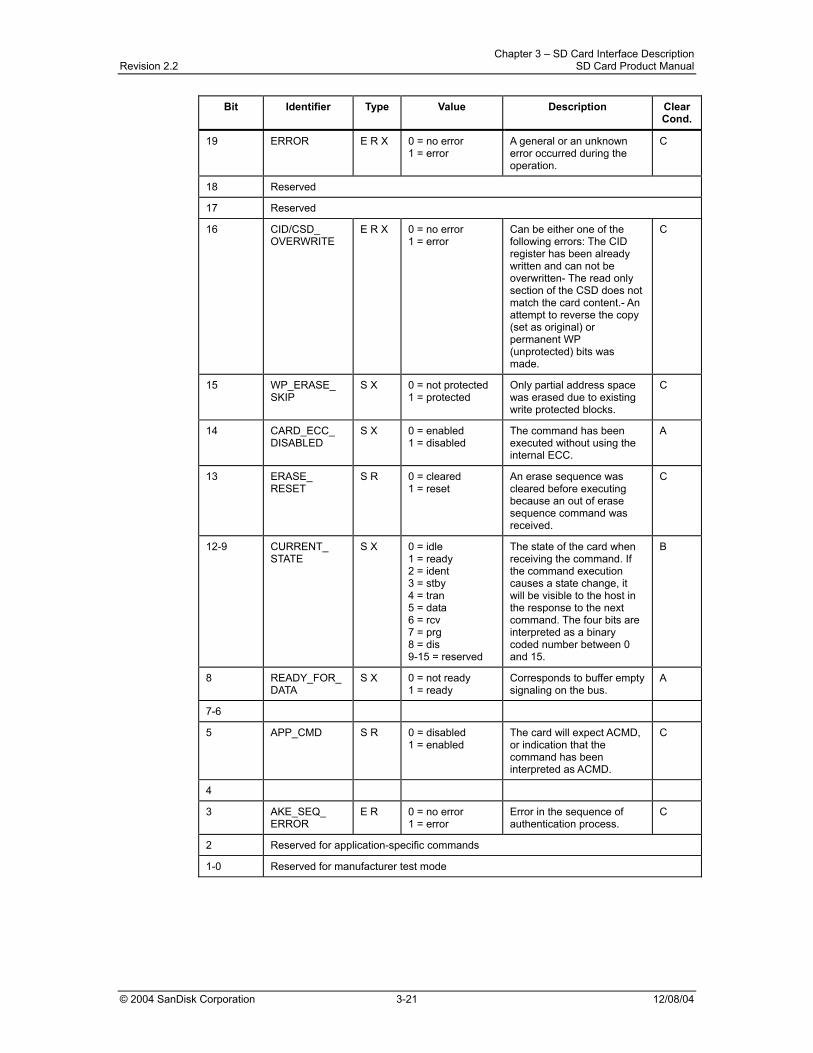
3.5.4 Status Register
The SD Card Status Register structure is defined in Table 3-29. The Type and Clear Condition fields in the table are coded as follows:
Type: • E—Error bit • S—Status bit • R—Detected and set for the actual command response • X—Detected and set during command execution. The host must poll the card by
sending status command in order to read these bits. Clear Condition: • A—According to the card current state • B—Always related to the previous command. Reception of a valid command will clear
it (with a delay of one command) • C—Clear by read.
Table 3-29 Status Register Description
Bit Identifier Type Value Description Clear Cond.
31 OUT_OF_ RANGE
E R X 0 = no error 1 = error
The command’s argument was out of the allowed range for this card.
C
30 ADDRESS_ ERROR
E R X 0 = no error 1 = error
A misaligned address that did not match the block length was used in the command.
C
29 BLOCK_LEN_ERROR
E R X 0 = no error 1 = error
The transferred block length is not allowed for this card, or the number of transferred bytes does not match the block length.
C
28 ERASE_SEQ_ERROR
E R 0 = no error 1 = error
An error in the sequence of erase commands occurred.
C
27 ERASE_ PARAM
E R X 0 = no error 1 = error
An invalid selection of write-blocks for erase occurred.
C
26 WP_ VIOLATION
E R X 0 = not protected 1 = protected
Attempt to program a write-protected block.
C
25 CARD_IS_ LOCKED
S X 0 = unlocked 1 = locked
When set, signals that the card is locked by the host
A
24 LOC_UNLOCK_FAILED
E R X 0 = no error 1 = error
Set when a sequence or password error has been detected in lock/ unlock card command or if there was an attempt to access a locked card
C
23 COM_CRC_ ERROR
E R 0 = no error 1 = error
The CRC check of the previous command failed
B
22 ILLEGAL_ COMMAND
E R 0 = no error 1 = error
Command not legal for the card state
B
21 CARD_ECC_ FAILED
E R X 0 = success 1 = failure
Card internal ECC was applied but failed to correct the data.
C
20 CC_ERROR E R X 0 = no error 1 = error
Internal card controller error C
Chapter 3 – SD Card Interface Description Revision 2.2 SD Card Product Manual
© 2004 SanDisk Corporation 3-21 12/08/04
Bit Identifier Type Value Description Clear Cond.
19 ERROR E R X 0 = no error 1 = error
A general or an unknown error occurred during the operation.
C
18 Reserved
17 Reserved
16 CID/CSD_ OVERWRITE
E R X 0 = no error 1 = error
Can be either one of the following errors: The CID register has been already written and can not be overwritten- The read only section of the CSD does not match the card content.- An attempt to reverse the copy (set as original) or permanent WP (unprotected) bits was made.
C
15 WP_ERASE_ SKIP
S X 0 = not protected 1 = protected
Only partial address space was erased due to existing write protected blocks.
C
14 CARD_ECC_ DISABLED
S X 0 = enabled 1 = disabled
The command has been executed without using the internal ECC.
A
13 ERASE_ RESET
S R 0 = cleared 1 = reset
An erase sequence was cleared before executing because an out of erase sequence command was received.
C
12-9 CURRENT_ STATE
S X 0 = idle 1 = ready 2 = ident 3 = stby 4 = tran 5 = data 6 = rcv 7 = prg 8 = dis 9-15 = reserved
The state of the card when receiving the command. If the command execution causes a state change, it will be visible to the host in the response to the next command. The four bits are interpreted as a binary coded number between 0 and 15.
B
8 READY_FOR_DATA
S X 0 = not ready 1 = ready
Corresponds to buffer empty signaling on the bus.
A
7-6
5 APP_CMD S R 0 = disabled 1 = enabled
The card will expect ACMD, or indication that the command has been interpreted as ACMD.
C
4
3 AKE_SEQ_ ERROR
E R 0 = no error 1 = error
Error in the sequence of authentication process.
C
2 Reserved for application-specific commands
1-0 Reserved for manufacturer test mode
Chapter 3 – SD Card Interface Description Revision 2.2 SD Card Product Manual
© 2004 SanDisk Corporation 3-22 12/08/04
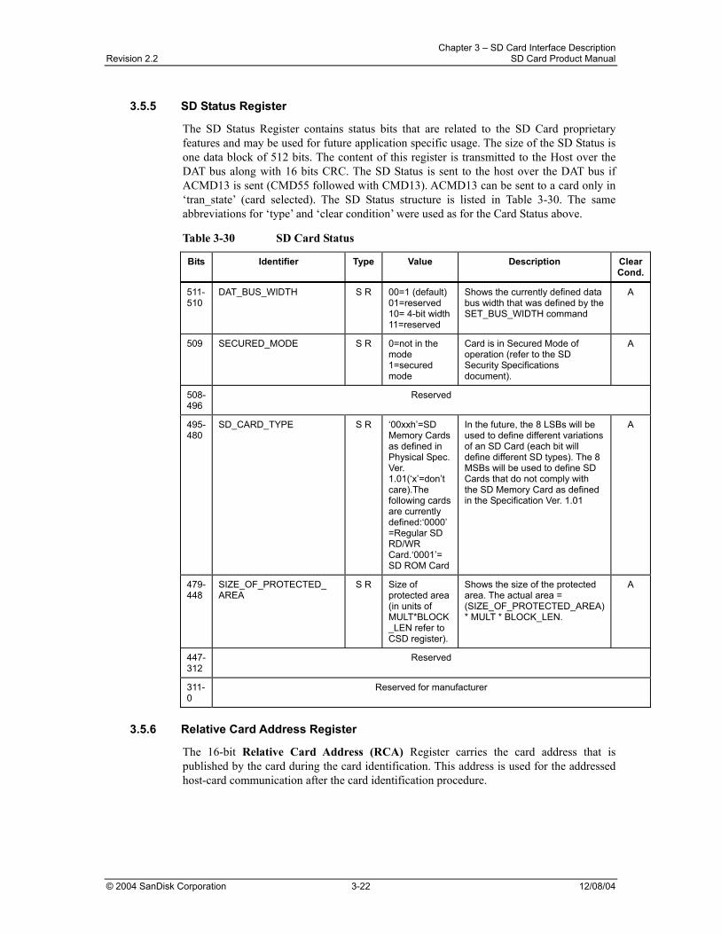
3.5.5 SD Status Register
The SD Status Register contains status bits that are related to the SD Card proprietary features and may be used for future application specific usage. The size of the SD Status is one data block of 512 bits. The content of this register is transmitted to the Host over the DAT bus along with 16 bits CRC. The SD Status is sent to the host over the DAT bus if ACMD13 is sent (CMD55 followed with CMD13). ACMD13 can be sent to a card only in ‘tran_state’ (card selected). The SD Status structure is listed in Table 3-30. The same abbreviations for ‘type’ and ‘clear condition’ were used as for the Card Status above.
Table 3-30 SD Card Status
Bits Identifier Type Value Description Clear Cond.
511-510
DAT_BUS_WIDTH S R 00=1 (default) 01=reserved 10= 4-bit width 11=reserved
Shows the currently defined data bus width that was defined by the SET_BUS_WIDTH command
A
509 SECURED_MODE S R 0=not in the mode 1=secured mode
Card is in Secured Mode of operation (refer to the SD Security Specifications document).
A
508-496
Reserved
495-480
SD_CARD_TYPE S R ‘00xxh’=SD Memory Cards as defined in Physical Spec. Ver. 1.01(‘x’=don’t care).The following cards are currently defined:‘0000’=Regular SD RD/WR Card.‘0001’= SD ROM Card
In the future, the 8 LSBs will be used to define different variations of an SD Card (each bit will define different SD types). The 8 MSBs will be used to define SD Cards that do not comply with the SD Memory Card as defined in the Specification Ver. 1.01
A
479-448
SIZE_OF_PROTECTED_ AREA
S R Size of protected area (in units of MULT*BLOCK_LEN refer to CSD register).
Shows the size of the protected area. The actual area = (SIZE_OF_PROTECTED_AREA) * MULT * BLOCK_LEN.
A
447-312
Reserved
311-0
Reserved for manufacturer
3.5.6 Relative Card Address Register
The 16-bit Relative Card Address (RCA) Register carries the card address that is published by the card during the card identification. This address is used for the addressed host-card communication after the card identification procedure.
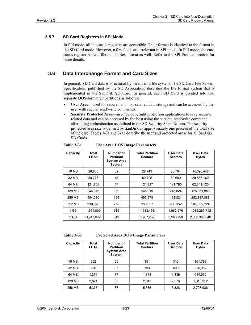
Chapter 3 – SD Card Interface Description Revision 2.2 SD Card Product Manual
© 2004 SanDisk Corporation 3-23 12/08/04
3.5.7 SD Card Registers in SPI Mode
In SPI mode, all the card’s registers are accessible. Their format is identical to the format in the SD Card mode. However, a few fields are irrelevant in SPI mode. In SPI mode, the card status register has a different, shorter, format as well. Refer to the SPI Protocol section for more details.
3.6 Data Interchange Format and Card Sizes
In general, SD Card data is structured by means of a file system. The SD Card File System Specification, published by the SD Association, describes the file format system that is implemented in the SanDisk SD Card. In general, each SD Card is divided into two separate DOS-formatted partitions as follows: • User Area—used for secured and non-secured data storage and can be accessed by the
user with regular read/write commands. • Security Protected Area—used by copyright protection applications to save security
related data and can be accessed by the host using the secured read/write command after doing authentication as defined in the SD Security Specification. The security protected area size is defined by SanDisk as approximately one percent of the total size of the card. Tables 3-31 and 3-32 describe the user and protected areas for all SanDisk SD Cards.
Table 3-31 User Area DOS Image Parameters
Capacity Total LBAs
Number of Partition
System Area Sectors
Total Partition Sectors
User Data Sectors
User Data Bytes
16 MB 28,800 39 28,743 28,704 14,696,448
32 MB 59,776 45 59,725 59,680 30,556,160
64 MB 121,856 57 121,817 121,760 62,341,120
128 MB 246,016 95 245,919 245,824 125,861,888
256 MB 494,080 155 493,979 493,824 252,837,888
512 MB 990,976 275 990,627 990,352 507,060,224
1 GB 1,984,000 519 1,983,495 1,982,976 1,015,283,712
2 GB 3,917,072 519 3,967,239 3,966,720 2,030,960,640
Table 3-32 Protected Area DOS Image Parameters
Capacity Total LBAs
Number of Partition
System Area Sectors
Total Partition Sectors
User Data Sectors
User Data Bytes
16 MB 352 35 351 316 161,792
32 MB 736 37 733 696 356,352
64 MB 1,376 37 1,373 1,336 684,032
128 MB 2,624 35 2,611 2,576 1,318,912
256 MB 5,376 37 5,365 5,328 2,727,936
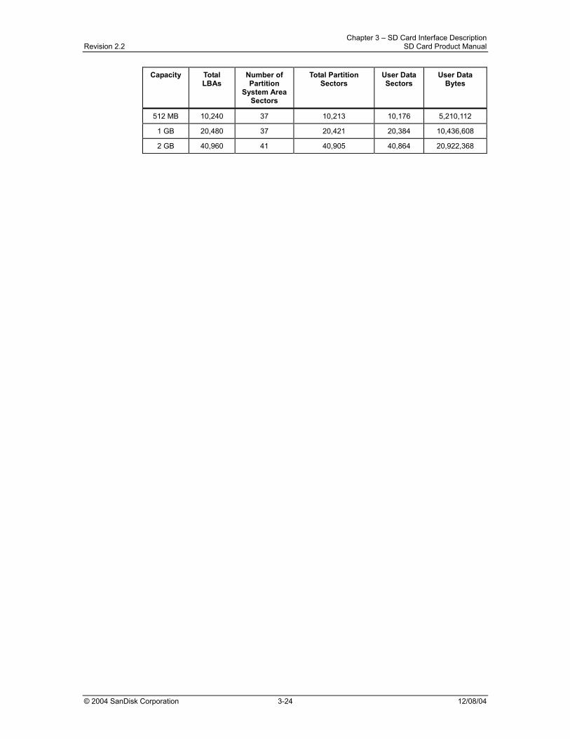
Chapter 3 – SD Card Interface Description Revision 2.2 SD Card Product Manual
© 2004 SanDisk Corporation 3-24 12/08/04
Capacity Total LBAs
Number of Partition
System Area Sectors
Total Partition Sectors
User Data Sectors
User Data Bytes
512 MB 10,240 37 10,213 10,176 5,210,112
1 GB 20,480 37 20,421 20,384 10,436,608
2 GB 40,960 41 40,905 40,864 20,922,368
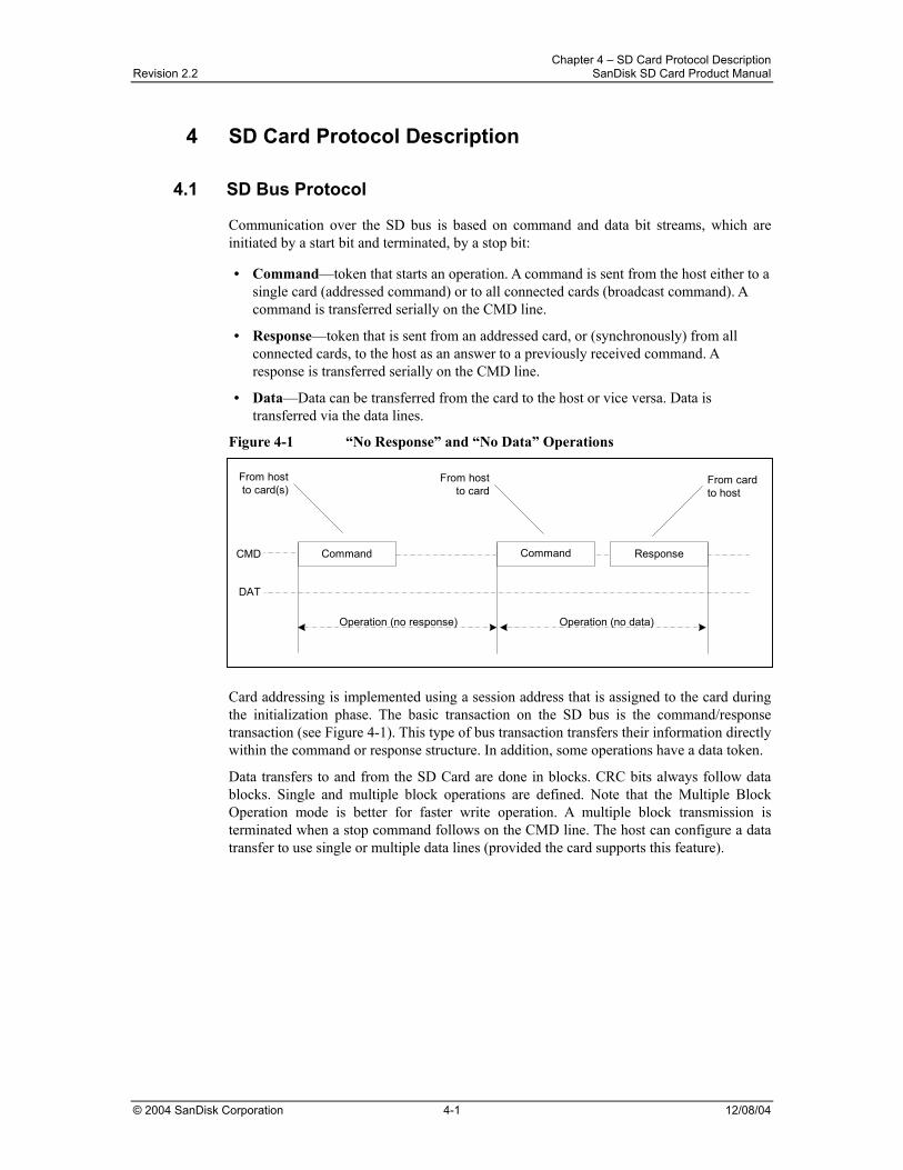
Chapter 4 – SD Card Protocol Description Revision 2.2 SanDisk SD Card Product Manual
© 2004 SanDisk Corporation 4-1 12/08/04
4 SD Card Protocol Description
4.1 SD Bus Protocol
Communication over the SD bus is based on command and data bit streams, which are initiated by a start bit and terminated, by a stop bit:
• Command—token that starts an operation. A command is sent from the host either to a single card (addressed command) or to all connected cards (broadcast command). A command is transferred serially on the CMD line.
• Response—token that is sent from an addressed card, or (synchronously) from all connected cards, to the host as an answer to a previously received command. A response is transferred serially on the CMD line.
• Data—Data can be transferred from the card to the host or vice versa. Data is transferred via the data lines.
Figure 4-1 “No Response” and “No Data” Operations
Card addressing is implemented using a session address that is assigned to the card during the initialization phase. The basic transaction on the SD bus is the command/response transaction (see Figure 4-1). This type of bus transaction transfers their information directly within the command or response structure. In addition, some operations have a data token.
Data transfers to and from the SD Card are done in blocks. CRC bits always follow data blocks. Single and multiple block operations are defined. Note that the Multiple Block Operation mode is better for faster write operation. A multiple block transmission is terminated when a stop command follows on the CMD line. The host can configure a data transfer to use single or multiple data lines (provided the card supports this feature).
CommandCMD
From hostto card(s)
DAT
From cardto host
ResponseCommand
Operation (no response) Operation (no data)
From hostto card
Chapter 4 – SD Card Protocol Description Revision 2.2 SanDisk SD Card Product Manual
© 2004 SanDisk Corporation 4-2 12/08/04
Figure 4-2 Multiple Block Read Operation
The block-write operation uses a simple busy signaling of the write operation duration on the DAT0 data line (see Figure 4-3) regardless of the number of data lines used for transferring the data.
Figure 4-3 Multiple Block Write Operation
Command tokens have the coding scheme shown in Figure 4-4.
Figure 4-4 Command Token Format
CMD
From hostto card(s)
DAT
Data fromcard tohost
ResponseCommand
Block write operation Data stop operation
Response
From cardto host
"Stop" command stopsdata transfer
Command
Data block CRC BusyData block CRC Busy
Multiple Block Write Operation
CRC OKresponseand busyfrom card
"Start" bitalways 0 "End" bit
always 1
Total length = 48 bits
0 Content CRC
Command content: command andaddress information or parameter,protected by 7-bit CRC checksum
1 1
"Transmitter" bit:1=host command
CMD
From hostto card(s)
DAT
Data fromcard tohost
ResponseCommand
Block read operation Data stop operation
Response
Data block CRC Data block CRC
From cardto host
"Stop" command stopsdata transfer
Data block CRC
Command
Multiple block read operation
Chapter 4 – SD Card Protocol Description Revision 2.2 SanDisk SD Card Product Manual
© 2004 SanDisk Corporation 4-3 12/08/04
Each command token is preceded by a start bit (0) and succeeded by an end bit (1). The total length is 48 bits. CRC bits protect each token to detect transmission errors; the operation may be repeated.
Response tokens have four coding schemes depending on their content. The token length is either 48 or 136 bits. The CRC protection algorithm for block data is a 16-bit CCITT polynomial. All used CRC types are described in Section 4.6
Figure 4-5 Response Token Format
In the CMD line, the MSB bit is transmitted first, whereas the LSB bit is transmitted last.
When the wide-bus option is used, the data is transferred four bits at a time (see Figure 4-6). Start and end bits, as well as the CRC bits, are transmitted for every one of the DAT lines. CRC bits are calculated and checked for every DAT line individually. The card sends the host the CRC status response and busy indication on DAT0 only. (DAT1-DAT3 during that period is “don’t care”).
Figure 4-6 Data Packet Format
"Start" bitalways 0 "End" bit
always 1
Response-content mirrored command andstatus information (R1 response). OCR Register(R3 response) or RCA (R6) protected by 7-bitCRC checksum
"Transmitter" bit:1=card response
Total length = 48 bits
0 Content0 1
Total length = 136 bits
0 Content= CID or CSD CRC0 1
"End" bitalways 1R1, R3, R6
R2
"Start" bitalways 0
"End" bitalways 1
MSB (4095)
Block length
0
Block length /4
"End" bitalways 1
LSB (0)
Standard busy(only DAT0 used)
CRC 1
DAT3 0 CRC4095 13
DAT2 0 CRC4094 12
DAT1 0 CRC4093 11
DAT0 0 CRC4092 10
MSN LSN
Widebus (all
four datalinesused)
Chapter 4 – SD Card Protocol Description Revision 2.2 SanDisk SD Card Product Manual
© 2004 SanDisk Corporation 4-4 12/08/04
4.2 Functional Description
The host (master) controls all communication between it and the SD Card. The host sends the following two types of commands:
• Broadcast Commands— Broadcast commands are intended for all SD cards. Some of these commands require a response.
• Addressed (Point-to-Point) Commands— The addressed commands are sent to the addressed SD Card and cause a response to be sent from this card.
A general overview of the command flow is shown in Figure 4-7 for the Card Identification Mode and in Figure 4-8 for the Data Transfer Mode. The commands are listed in Tables 4-15 and 4-16. The dependencies among the current SD Card, received-command and following states are listed in Table 4-18. In the following sections, the various card operation modes will be described first. Thereafter, the restrictions for controlling the clock signal are defined. All SD Card commands, together with corresponding responses, state transitions, error conditions, and timings are presented in the following sections.
The SanDisk SD Card has two operation modes.
• Card Identification Mode— The host will be in card identification mode after reset and while it is looking for new cards on the bus. SD cards will be in this mode after reset until the SET_RCA command (CMD3) is received.
• Data Transfer Mode— SD cards will enter data-transfer mode when their RCA is first published. The host will enter data-transfer mode after identifying all SD cards on the bus.
Table 4-1 lists the dependencies between operation modes and card states. Each state in the card state diagrams (Figure 4-7 and 4-8) is associated with one operation mode.
Table 4-1 Card States vs. Operation Modes Overview
Card State Operation Mode
Inactive Inactive
Idle, Ready, Identification Card Identification Mode
Standby, Transfer, Send data, Receive data, Programming, Disconnect
Data Transfer Mode
4.3 Card Identification Mode In Card Identification Mode the host resets all cards, validates operation voltage range, identifies and requests cards to publish a Relative Card Address (RCA). This operation is performed on each card separately using its own command (CMD) line. All data communication in the Card Identification Mode uses the CMD line only.
Chapter 4 – SD Card Protocol Description Revision 2.2 SanDisk SD Card Product Manual
© 2004 SanDisk Corporation 4-5 12/08/04
Figure 4-7 SD Memory Card State Diagram—Card Identification Mode
4.3.1 Reset
The GO_IDLE_STATE (CMD0) is the software-reset command that makes each SD Card move into an idle state regardless of the card’s current state. Cards already in an inactive state are not affected by this command.
After power-on by the host, all cards are in an idle state, including cards that were in an inactive state.1
After power-on or CMD0, all card CMD lines are in input mode, waiting for the start-bit of the next command. The cards are initialized with a default relative card address (RCA=0x0000) and a default driver-stage-register setting (lowest speed, highest driving current capability).
4.3.2 Operating Voltage Range Validation
The physical specification standard, defined by the SDA, requires that all SD cards can use any operating voltage between VDD-min and VDD-max to establish communication with the host. However, during data transfer, minimum and maximum values for VDD are defined in the Operations Condition Register (OCR) and may not cover the entire range. Card hosts are expected to read the CSD Register and select proper VDD values or reject the card.
An SD Card that stores the CID and CSD data in the payload memory can communicate this information under data-transfer VDD conditions only. In other words, if the host and
1 At least 74 clock cycles are required prior to starting bus communication.
Idle State (idle)
ACMD41
Ready State(ready)
CMD2
Identification State(ident)
CMD3
Standby State(stby) CMD3
Inactive State (ina) CMD15
CMD0
CMD0CS Asserted (0)
SPI OperationMode From all states
except "ina"
Card respondsw/new RCA
From all states inData Transfer
Mode
Card respondsw/new RCA
Start MMCinitialization process
starting at CMD1
No response (nonvalid command)must be an MMC
Card is busy orhost omitted
voltage range
Cards w/non-compatible voltage range
Card Identification Mode
Data Transfer Mode
Power On
Chapter 4 – SD Card Protocol Description Revision 2.2 SanDisk SD Card Product Manual
© 2004 SanDisk Corporation 4-6 12/08/04
card have incompatible VDD ranges, the card will not be able to complete the identification cycle or send CSD data.
The SD_SEND_OP_COND (ACMD41) command is designed to provide card hosts with a mechanism to identify and reject cards that do not match the host’s desired VDD range. To accomplish this, the host sends the required VDD voltage window as the operand of the command. SD cards that cannot perform data transfers in the specified range must discard themselves from further bus operations and go into Inactive State2.
The MultiMediaCard will not respond to ACMD413. The MultiMediaCard will be initialized per the MultiMediaCard specification, using SEND_OP_COND command (CMD1). The host should ignore an ILLEGAL_COMMAND status in the response to CMD3, since it is a residue of ACMD41 that is invalid in the MultiMediaCard (CMD0, 1, 2 do not clear the Status Register). The host will use ACMD41 and CMD1 in a system, to distinguish between a MultiMediaCard and an SD Card.
By omitting the voltage range in the command, the host can query each card and determine if there are any incompatibilities before sending out-of-range cards into an inactive state. This query should be used if the host can select a common voltage range or wants to notify the application of non-usable cards in the stack.
The SanDisk SD Card can use the busy bit in the ACMD41 response to tell the host that it is still working on its power-up/reset procedure (e.g., downloading the register information from memory field) and is not ready for communication. In this case the host must repeat ACMD41 until the busy bit is cleared.
During the initialization procedure, the host is not allowed to change the OCR values; the SD Card will ignore changes in the OCR content. If there is a real change in the operating conditions, the host must reset the card stack (using CMD0) and begin the initialization procedure once more. However, for accessing cards already in Inactive State, a hard reset must be done by switching the power supply off and on.
GO_INACTIVE_STATE (CMD15) can also be used to send an addressed SD Card into the inactive state. CMD15 is used when the host explicitly wants to deactivate a card—for example, the host changes VDD into a range not supported by this card.
4.3.3 Card Identification Process
The host starts the card identification process with the identification clock rate fOD. In the SD Card, the CMD line output drives are push-pull drivers.
After the bus is activated, the host will request the cards to send their valid operation conditions (ACMD41 preceding with APP_CMD-CMD55 with RCA=0x0000). The response to ACMD41 is the Operation Condition Register of the card. The same command will be sent to all of the new cards in the system. Incompatible cards are sent into inactive state. The host then issues the command, ALL_SEND_CID (CMD2), to each card to get its unique card identification (CID) number. An unidentified card (i.e., which is in Ready State) sends its CID number as the response (on the CMD line). After the card sends the CID number, it goes into Identification State. Thereafter, the host issues the CMD3 (SEND_RELATIVE_ADDR) command asking the card to publish a new relative card address (RCA), which is shorter than CID and will be used to address the card in the future data transfer mode (typically with a higher clock rate than fOD).
2 ACMD41 is an application-specific command. Therefore, APP_CMD (CMD55) will always precede ACMD41. The RCA to be used for CMD55 in idle_state will be the card’s default RCA = 0x0000. 3Actually it will not respond to preceding commands APP_CMD-CMD55.
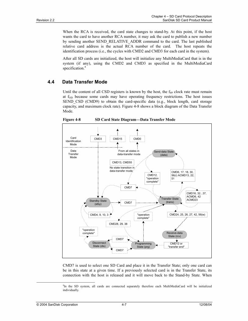
Chapter 4 – SD Card Protocol Description Revision 2.2 SanDisk SD Card Product Manual
© 2004 SanDisk Corporation 4-7 12/08/04
When the RCA is received, the card state changes to stand-by. At this point, if the host wants the card to have another RCA number, it may ask the card to publish a new number by sending another SEND_RELATIVE_ADDR command to the card. The last published relative card address is the actual RCA number of the card. The host repeats the identification process (i.e., the cycles with CMD2 and CMD3 for each card in the system).
After all SD cards are initialized, the host will initialize any MultiMediaCard that is in the system (if any), using the CMD2 and CMD3 as specified in the MultiMediaCard specification.4
4.4 Data Transfer Mode
Until the content of all CSD registers is known by the host, the fPP clock rate must remain at fOD because some cards may have operating frequency restrictions. The host issues SEND_CSD (CMD9) to obtain the card-specific data (e.g., block length, card storage capacity, and maximum clock rate). Figure 4-8 shows a block diagram of the Data Transfer Mode.
Figure 4-8 SD Card State Diagram—Data Transfer Mode
CMD7 is used to select one SD Card and place it in the Transfer State; only one card can be in this state at a given time. If a previously selected card is in the Transfer State, its connection with the host is released and it will move back to the Stand-by State. When
4In the SD system, all cards are connected separately therefore each MultiMediaCard will be initialized individually.
ProgrammingState (prg)
CMD13, CMD55
CMD7
DisconnectState (dis)
CMD4, 9, 10, 3
Standby State(stby)
CMD12 or"transfer end"
Receive-dataState (rcv)
CMD16, 32...37,ACMD6, 42ACMD23
No state transition indata-transfer mode
From all states indata-transfer mode
CardIdentification
Mode
CMD3
"operationcomplete"
CMD15 CMD0
CMD7
CMD28, 29, 38
CMD7
CMD7
"operationcomplete"
DataTransfer
Mode
CMD24, 25, 26, 27, 42, 56(w)
CMD6, 17, 18, 30,56(r) ACMD13, 22,51
Send-data State(data)
CMD12,"operationcomplete"
Transfer State(trans)
Chapter 4 – SD Card Protocol Description Revision 2.2 SanDisk SD Card Product Manual
© 2004 SanDisk Corporation 4-8 12/08/04
CMD7 is issued with the reserved relative card address “0x0000,” all cards transfer back to Stand-by State. This may be used before identifying new cards without resetting other already registered cards. Cards that already have an RCA do not respond to identification command flow in this state.
Important: Card de-selection occurs if a specific card retrieves a CMD7 command with an unmatched RCA. This happens automatically if another card is selected and the CMD lines are common. Therefore, in the SD Card system, it will be the responsibility of the host to do either of the following.
− Work with the common CMD line (after initialization is complete)). In this case the card de-selection will be done automatically (similarly to the MMC system).
− Be aware of the necessity to de-select cards if the CMD lines are separate. All data communication in the Data Transfer Mode is point-to-point between the host and the selected SD Card (using addressed commands). All addressed commands are acknowledged with a response on the CMD line.
The relationship between the various data transfer modes is summarized in Figure 4-8. More detailed information is listed below.
• The stop command (CMD12) can abort all data read commands at any given time. The data transfer will terminate and the card will return to the Transfer State. The read commands are block read (CMD17), multiple block read (CMD18), send write-protect (CMD30), send SCR (ACMD51) and general command in read mode (CMD56).
• The stop command (CMD12) can abort all data write commands at any given time. The write commands must be stopped prior to de-selecting the card with CMD7. The write commands are block write (CMD24 and CMD25), write CSD (CMD27), lock/unlock command (CMD42) and general command in write mode (CMD56).
• When the data transfer is complete, the SD Card exits the Data Write State and moves to either the Programming State (successful transfer) or Transfer State (failed transfer).
• If a block write operation is stopped and the block length and CRC of the last block are valid, the data will be programmed
• The card may provide buffering for block write: the next block can be sent to the card while the previous is being programmed. If all write buffers are full, and the SD Card is in Programming State (refer to Figure 4-8), the DAT0 line will be kept low.
• No buffering option is available for write CSD, write protection, and erase: no other data transfer commands will be accepted when the SD Card is busy servicing any one of the aforementioned commands. DAT0 line will be kept low as long as the card is busy and in the Programming State. Actually if the CMD and DAT0 lines of the cards are kept separate and the host keeps the busy DAT0 line disconnected from the other DAT0 lines (of the other cards), the host may access the other cards while the card is in busy.
• Parameter-set commands are not allowed when the card is programming. Parameter-set commands are set block length (CMD16), erase block start (CMD32) and erase block end (CMD33).
• Read commands are not allowed while the card is programming.
• Moving another card from Stand-by to Transfer State (using CMD7) will not terminate a programming operation. The card will switch to the Disconnect State and release the DAT line.
Chapter 4 – SD Card Protocol Description Revision 2.2 SanDisk SD Card Product Manual
© 2004 SanDisk Corporation 4-9 12/08/04
• A card can be re-selected while in the Disconnect State, using CMD7. In that case, the card will move to the Programming State and reactivate the busy indication.
• Resetting the card (using CMD0 or CMD15) will terminate any pending or active programming operation, which may destroy the data contents on the card. It is the host’s responsibility to prevent the potential destruction of data.
4.4.1 2-GB Card
To make a 2-GB card, the Maximum Block Length (READ_BL_LEN=WRITE_BL_LEN) will be set to 1024 bytes. But Block Length set by CMD16 must be up to 512 bytes to stay consistent with 512 bytes Maximum Block Length cards (less than and equal 2-GB cards).
4.4.2 Wide Bus Selection/De-selection
Wide bus (4-bit bus width) operation mode may be selected/de-selected using ACMD6. The default bus width after power up or GO_IDLE (CMD) is one-bit bus width. ACMD6 command is valid in tran state only. That means that the bus width may be changed only after a card has been selected (CMD7).
4.4.3 Data Read Format
When data is not being transmitted, the DAT bus line is high. A transmitted data block consists of a start bit (low), followed by a continuous data stream. The data stream contains the net payload data, and error correction bits if an off-card ECC is used. The data stream ends with an end bit (high). The data transmission is synchronous to the clock signal
The payload for a block-oriented data transfer is preserved by a CRC checksum. The generator polynomial is standard CCITT format: x16 + x12 + x5 + 1.
Block Read The basic unit of data transfer is a block whose maximum size is defined by READ_BL_LEN in the CSD Register. Smaller blocks with a starting and ending address contained entirely within one physical block, as defined by READ_BL_LEN, may also be transmitted. A CRC appended to the end of each block ensures data transfer integrity. CMD17 or READ_SINGLE_BLOCK starts a block read and returns the card to the Transfer State after a complete transfer. CMD18 or READ_MULTIPLE_BLOCK starts a transfer of several consecutive blocks. Blocks will be continuously transferred until a stop command is issued. The stop command has an execution delay due to the serial command transmission. The data transfer stops after the end bit of the stoop command.
If the host uses partial blocks with an accumulated length that is not block-aligned, the card, at the beginning of the first misaligned block, will detect a block misalignment error, set the ADDRESS_ERROR bit in the Status Register, abort transmission, and wait in the Data State for a stop command.
4.4.4 Data Write Format
The data transfer format is similar to the data read format. For block-oriented write data transfer, the CRC check bits are added to each data block. Prior to an operation, the card performs a CRC check for each such received data block.5 This mechanism prevents the erroneous writing of transferred data.
5The polynomial is the same one used for a read operation.
Chapter 4 – SD Card Protocol Description Revision 2.2 SanDisk SD Card Product Manual
© 2004 SanDisk Corporation 4-10 12/08/04
Block Write Block write (CMD24-27, 42, 56(w)) means that one or more blocks of data are transferred from the host to the card with a 1-bit or 4-bit CRC appended to the end of each block by the host. SanDisk SD cards that support block-write are require the block length, set by CMD16, to be 512 bytes regardless of whether WRITE_BL_LEN is set to 1k or 2kBytes.
The following table defines the card behavior when partial-block access is disabled (WRITE_BL_PARTIAL = 0).
Table 4-2 Write Command Block Length
CSD Value
Max block size WRITE_BL_LEN
Misalign Partial
Current Blocklen6
Write CMD Start Address7
512-Bytes 0 (disable) 0 (disable) 512 bytes n * 512 bytes (n : Integer)
1-kBytes 0 (disable) 0 (disable) 512 bytes n * 512 bytes (n : Integer)
2-kBytes 0 (disable) 0 (disable) 512 bytes n * 512 bytes (n : Integer)
In Table 4-2, the size in the “Current Blocklen” field is set or changed by CMD16. If the value is less than 512 bytes (there are no relations with misalign and partial option), it is set with no error. Then the size of the current block length is tested when the write command is executed.
If WRITE_BL_PARTIAL is allowed (=1) then smaller blocks, up to resolution of one byte, can be used as well. If the CRC fails, the card shall indicate the failure on the DAT line (see below); the transferred data will be discarded and not written, and all further transmitted blocks (in multiple block write mode) will be ignored.
Multiple block-write command shall be used rather than continuous single write command to make faster write operation.
If the host uses partial blocks whose accumulated length is not block aligned and block misalignment is not allowed (CSD parameter WRITE_BLK_MISALIGN is not set), the card shall detect the block misalignment error and abort programming before the beginning of the first misaligned block.
The card shall set the ADDRESS_ERROR error bit in the status register, and while ignoring all further data transfer, wait in the Receive-data-State for a stop command.
The write operation shall also be aborted if the host tries to write over a write-protected area. In this case, however, the card will set the WP_VIOLATION bit. Programming of the CSD register does not require a previous block length setting. The transferred data is also CRC protected. If a part of the CSD register is stored in ROM, then this unchangeable part must match the corresponding part of the receive buffer. If this match fails, then the card will report an error and not change any register contents.
Some cards may require long and unpredictable times to write a block of data. After receiving a block of data and completing the CRC check, the card will begin writing and hold the DAT0 line low if its write buffer is full and unable to accept new data from a new WRITE_BLOCK command. The host may poll the status of the card with a SEND_STATUS command (CMD13) at any time, and the card will respond with its status. The status bit READY_FOR_DATA indicates whether the card can accept new data or
6 If the current block length is other than the values in the column, the SD Card indicates BLOCK_LEN_ERROR” on the write-command response. 7If the start address is different than the values in the column, the card will send “ADDRESS_ERROR” on the Write command response.
Chapter 4 – SD Card Protocol Description Revision 2.2 SanDisk SD Card Product Manual
© 2004 SanDisk Corporation 4-11 12/08/04
whether the write process is still in progress). The host may deselect the card by issuing CMD7 (to select a different card) that will displace the card into the Disconnect State and release the DAT line without interrupting the write operation. When reselecting the card, it will reactivate busy indication by pulling DAT to low if programming is still in progress and the write buffer is unavailable. Actually, the host may perform simultaneous write operation to several cards with inter-leaving process. The interleaving process can be done by accessing each card separately while other cards are busy. This process can be done by proper CMD and DAT0-3 line manipulations (disconnection of busy cards).
Send Number of Written Blocks
Systems that use the PipeLine mechanism for data buffers management are, in some cases, unable to determine which block was the last to be well written to the flash if an error occurs in the middle of a Multiple Blocks Write operation. The card will respond to ACMD22 with the number of well-written blocks.
4.4.5 Erase
Identification of write blocks is accomplished with the ERASE_WR_BLK_START (CMD32), ERASE_WR_BLK_END (CMD33) commands.
The host must adhere to the following command sequence: ERASE_WR_BLK_START, ERASE_WR_BLK_END and ERASE (CMD38).
If an erase (CMD38) or address setting (CMD32, 33) command is received out of sequence, the card sets the ERASE_SEQ_ERROR bit in the Status Register and reset the entire sequence.
If an out-of-sequence command (except SEND_STATUS) is received, the card will set the ERASE_RESET status bit in the Status Register, reset the erase sequence and execute the last command.
If the erase range includes write-protected sectors, they will be left intact and only the unprotected sectors will be erased. The WP_ERASE_SKIP status bit in the Status Register will be set.
The address field in the address setting commands is a write block address in byte units. The card ignores all LSBs below the WRITE_BLK_LEN (see CSD) size.
As described above for block write, the card will indicate that an erase is in progress by holding DAT0 low. The actual erase time may be long, and the host may issue CMD7 to de-select the card or perform card disconnection, as described in the Block Write section, above.
The card data after an erase operation is either “0” or “1”, depending on the card vendor. The SCR register bit DATA_STAT_AFTER_ERASE (bit 55) defines whether it is “0” or “1”.
4.4.6 Write Protect Management
Three write-protect methods are supported in the SD Card as follows.
• Mechanical write-protect switch (host responsibility only)
• Card internal write-protect (card’s responsibility)
• Password protection card-lock operation
Chapter 4 – SD Card Protocol Description Revision 2.2 SanDisk SD Card Product Manual
© 2004 SanDisk Corporation 4-12 12/08/04
Mechanical Write Protect Switch
A mechanical sliding tablet on the side of the card (refer to the mechanical description), controlled by the user, indicates whether or not a given card is write-protected. If the sliding tablet is in the position of the window open, it means the card is write-protected. If the window is closed, the card is not write-protected.
A proper, matched, switch on the socket side will indicate to the host that the card is write- protected or not. It is the responsibility of the host to protect the card. The position of the write-protect switch is unknown to the internal circuitry of the card.
Card’s Internal Write Protection (Optional)
Card data may be protected against either erase or write. The entire card may be permanently write-protected by the manufacturer or content provider by setting the permanent or temporary write protect bits in the CSD Register.
4.4.7 Card Lock/Unlock Operation
The password-protection feature enables the host to lock a card while providing a password that will be used later for unlocking the card. The password and its size are kept in 128-bit PWD and 8-bit PWD_LEN registers, respectively. These registers are non-volatile which protects a power cycle erase.
Locked cards respond to (and execute) all commands in the "basic" command class (class 0), ACMD41, CMD16 and “lock card” command class. Thus the host is allowed to reset, initialize, select, query for status, etc., but not to access data on the card. If the password was previously set (the value of PWD_LEN is not ‘0’), it will be locked automatically after power on.
Similar to the existing CSD Register write commands the lock/unlock command is available in "transfer state" only. This means that it does not include an address argument and the card has to be selected before using it.
The card lock/unlock command has the structure and bus transaction type of a regular single block write command. The transferred data block includes all the required information of the command (password setting mode, PWD itself, card lock/unlock etc.). The following table describes the structure of the command data block.
Table 4-3 Lock Card Data Structure
Byte Bit 7
Bit 6
Bit 5
Bit 4
Bit 3 Bit 2 Bit 1 Bit 0
0 Reserved ERASE LOCK_UNLOCK CLR_PWD SET_PWD
1 PWDS_LEN
2
…
PWDS_LEN + 1
Password Data
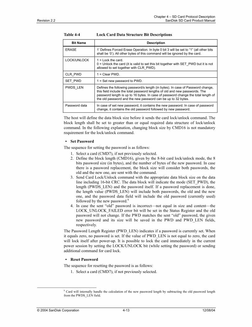
Chapter 4 – SD Card Protocol Description Revision 2.2 SanDisk SD Card Product Manual
© 2004 SanDisk Corporation 4-13 12/08/04
Table 4-4 Lock Card Data Structure Bit Descriptions
Bit Name Description
ERASE 1’ Defines Forced Erase Operation. In byte 0 bit 3 will be set to “1” (all other bits shall be ‘0’). All other bytes of this command will be ignored by the card.
LOCK/UNLOCK 1 = Lock the card. 0 = Unlock the card (it is valid to set this bit together with SET_PWD but it is not allowed to set together with CLR_PWD).
CLR_PWD 1 = Clear PWD.
SET_PWD 1 = Set new password to PWD.
PWDS_LEN Defines the following password/s length (in bytes). In case of Password change, this field include the total password lengths of old and new passwords. The password length is up to 16 bytes. In case of password change the total length of the old password and the new password can be up to 32 bytes.
Password data In case of set new password, it contains the new password. In case of password change, it contains the old password followed by new password.
The host will define the data block size before it sends the card lock/unlock command. The block length shall be set to greater than or equal required data structure of lock/unlock command. In the following explanation, changing block size by CMD16 is not mandatory requirement for the lock/unlock command.
• Set Password The sequence for setting the password is as follows:
1. Select a card (CMD7), if not previously selected. 2. Define the block length (CMD16), given by the 8-bit card lock/unlock mode, the 8
bits password size (in bytes), and the number of bytes of the new password. In case there is a password replacement, the block size will consider both passwords, the old and the new one, are sent with the command.
3. Send Card Lock/Unlock command with the appropriate data block size on the data line including 16-bit CRC. The data block will indicate the mode (SET_PWD), the length (PWDS_LEN) and the password itself. If a password replacement is done, the length value (PWDS_LEN) will include both passwords, the old and the new one, and the password data field will include the old password (currently used) followed by the new password.8
4. In case the sent “old” password is incorrect—not equal in size and content—the LOCK_UNLOCK_FAILED error bit will be set in the Status Register and the old password will not change. If the PWD matches the sent “old” password, the given new password and its size will be saved in the PWD and PWD_LEN fields, respectively.
The Password Length Register (PWD_LEN) indicates if a password is currently set. When it equals zero, no password is set. If the value of PWD_LEN is not equal to zero, the card will lock itself after power-up. It is possible to lock the card immediately in the current power session by setting the LOCK/UNLOCK bit (while setting the password) or sending additional command for card lock.
• Reset Password The sequence for resetting the password is as follows:
1. Select a card (CMD7), if not previously selected.
8 Card will internally handle the calculation of the new password length by subtracting the old password length from the PWDS_LEN field.
Chapter 4 – SD Card Protocol Description Revision 2.2 SanDisk SD Card Product Manual
© 2004 SanDisk Corporation 4-14 12/08/04
2. Define the block length (CMD16), given by the 8-bit card lock/unlock mode, the 8-bit password size (in bytes), and the number of bytes of the currently used password.
3. Send the card lock/unlock command with the appropriate data block size on the data line including 16 bit CRC. The data block shall indicate the mode CLR_PWD, the length (PWDS_LEN) and the password itself . If the PWD and PWD_LEN content match the sent password and its size, then the content of the PWD Register is cleared and PWD_LEN is set to 0. If the password is not correct, the LOCK_UNLOCK_FAILED error bit will be set in the Status Register.
• Lock Card The sequence for locking a card is as follows:
1. Select a card (CMD7), if not previously selected. 2. Define the block length (CMD16), given by the 8-bit card lock/unlock mode, the 8-
bit password size (in bytes), and the number of bytes of the currently used password.
3. Send the Card Lock/Unlock command with the appropriate data block size on the data line including 16-bit CRC. The data block indicates the mode (LOCK), the length (PWDS_LEN) and the password (PWD) itself.
If the PWD content equals to the sent password, the card will be locked and the card-locked status bit will be set in the Status Register. If the password is incorrect, the LOCK_UNLOCK_FAILED error bit will be set in the Status Register.
It is possible to set the password and to lock the card in the same sequence. In such case the host performs all the required steps for setting the password (as described above) including the bit LOCK set while the new password command is sent.
If the password was previously set (PWD_LEN is not 0), the card will be locked automatically after power-on reset.
An attempt to lock a locked card or to lock a card that does not have a password will fail and the LOCK_UNLOCK_FAILED error bit will be set in the Status Register unless it was done during a password definition or change operations.
• Unlock Card The sequence for unlocking a card is as follows:
1. Select a card (CMD7), if not selected already. 2. Define the block length (CMD16), given by the 8-bit card lock/unlock mode, the 8-
bit password size (in bytes), and the number of bytes of the currently used password.
3. Send the Card Lock/Unlock command with the appropriate data block size on the data line including 16-bit CRC. The data block will indicate the mode (UNLOCK), the length (PWDS_LEN) and the password (PWD) itself.
If the PWD content equals to the sent password, the card will be unlocked and the card-locked status bit will be cleared in the Status Register. If the password is incorrect, the LOCK_UNLOCK_FAILED error bit will be set in the Status Register.
Unlocking occurs only for the current power session. As long as the PWD is not cleared the card will be locked automatically on the next power-up. The only way to unlock the card is by clearing the password.
An attempt to unlock an unlocked card will fail and LOCK_UNLOCK_FAILED error bit will be set in the Status Register unless it was done during a password definition or change operations.
Chapter 4 – SD Card Protocol Description Revision 2.2 SanDisk SD Card Product Manual
© 2004 SanDisk Corporation 4-15 12/08/04
• Force Erase In case the user forgets the password (the PWD content) it is possible to erase all card data content along with the PWD content. This operation is called Forced Erase.
1. Select a card (CMD7), if not previously selected.
2. Define the block length (CMD16) to 1 byte (8-bit card lock/unlock command). Send the Card Lock/Unlock command with the appropriate data block of one byte on the data line including 16-bit CRC. The data block will indicate the mode ERASE (the ERASE bit will be the only bit set).
If the erase bit is not the only bit in the data field, the LOCK_UNLOCK_FAILED error bit will be set in the Status Register and the erase request is rejected. If the command was accepted, all card content is erased including the PWD and PWD_LEN Register content and the locked card will get unlocked.
An attempt to force erase on an unlocked card will fail and the LOCK_UNLOCK_FAILED error bit will be set in the Status Register.
• Parameter and Results of CMD42 The block length will be greater than or equal required data structure of CMD42; otherwise, the result of CMD42 is undefined and the card may be in the unexpected locked state. Table 4-5 clarifies the behavior of CMD42. The reserved bits in the parameter (bit7-4) of CMD42 are “don't care.”
In case CMD42 requires the password, it is assumed that the old password and the new password are set correctly; otherwise the card indicates error regardless of information contained in Table 4-5. If the password length is 0 or greater than 128 bits, the card indicates error. If errors occur during execution of CMD42, the LOCK_UNLOCK_FAILED (Bit24 of Card Status) will be set to 1 regardless of the information in Table 4-5.
The CARD_IS_LOCKED (Bit25 of Card Status) in the response of CMD42 will be the same as Current Card State. In the field of Card Status, "0” to 1" means the card change to Locked and "1 to 0" means the card change to Unlocked after execution of CMD42. It can be seen in the response of CMD13 after the CMD42.
The LOCK_UNLOCK_FAILED (Bit24 of Card Status) as the result of CMD42 can be seen in the response of either CMD42 or following CMD13.
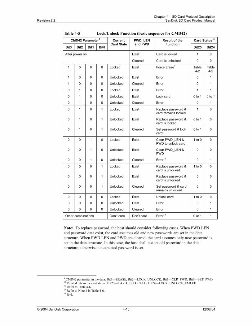
Chapter 4 – SD Card Protocol Description Revision 2.2 SanDisk SD Card Product Manual
© 2004 SanDisk Corporation 4-16 12/08/04
Table 4-5 Lock/Unlock Function (basic sequence for CMD42)
CMD42 Parameter9 Card Status10
Bit3 Bit2 Bit1 Bit0
Current Card State
PWD_LEN and PWD
Result of the Function
Bit25 Bit24
Exist Card is locked 1 0 After power on
Cleared Card is unlocked 0 0
1 0 0 0 Locked Exist Force Erase11 Table 4-2
Table 4-2
1 0 0 0 Unlocked Exist Error 0 1
1 0 0 0 Unlocked Cleared Error 0 1
0 1 0 0 Locked Exist Error 1 1
0 1 0 0 Unlocked Exist Lock card 0 to 1 0 to 1
0 1 0 0 Unlocked Cleared Error 0 1
0 1 0 1 Locked Exist Replace password & card remains locked
1 0
0 1 0 1 Unlocked Exist Replace password & card is locked
0 to 1 0
0 1 0 1 Unlocked Cleared Set password & lock card
0 to 1 0
0 0 1 0 Locked Exist Clear PWD_LEN & PWD to unlock card
1 to 0 0
0 0 1 0 Unlocked Exist Clear PWD_LEN & PWD
0 0
0 0 1 0 Unlocked Cleared Error12 0 1
0 0 0 1 Locked Exist Replace password & card is unlocked
1 to 0 0
0 0 0 1 Unlocked Exist Replace password & card is unlocked
0 0
0 0 0 1 Unlocked Cleared Set password & card remains unlocked
0 0
0 0 0 0 Locked Exist Unlock card 1 to 0 0
0 0 0 0 Unlocked Exist Error 0 1
0 0 0 0 Unlocked Cleared Error 0 1
Other combinations Don’t care Don’t care Error13 0 or 1 1
Note: To replace password, the host should consider following cases. When PWD LEN and password data exist, the card assumes old and new passwords are set in the data structure. When PWD LEN and PWD are cleared, the card assumes only new password is set in the data structure. In this case, the host shall not set old password in the data structure; otherwise, unexpected password is set.
9 CMD42 parameter in the data: Bit3—ERASE, Bit2—LOCK_UNLOCK, Bit1—CLR_PWD, Bit0—SET_PWD. 10 Related bits in the card status: Bit25—CARD_IS_LOCKED, Bit24—LOCK_UNLOCK_FAILED. 11 Refer to Table 4-6. 12 Refer to Note 1 in Table 4-6. 13 Ibid.
Chapter 4 – SD Card Protocol Description Revision 2.2 SanDisk SD Card Product Manual
© 2004 SanDisk Corporation 4-17 12/08/04
• Two types of Lock/Unlock Card There will be two types of lock / unlock function-supported cards. Type 1 is an older version of the SD Card, and Type 2 is the new version defined in this specification (v1.10). Table 4-6 shows the difference between these types of cards. The SD cards that support Lock /Unlock and comply with Version 1.01, can take either Type 1 or Type 2. SD cards that support Lock / Unlock and comply with Version 1.10, take Type 2.
Table 4-6 Type 1 vs. Type 2 Card of Lock/Unlock Function
Note Type 1 Card (older version) Type 2 Card (new version)
1 Treat CMD42 Parameter=0011b as 0001b.
Treat CMD42 Parameter=0111b as 0101b.
Treat CMD42 Parameter=0110b as 0010b.
Results of other combinations are Error.
All results are each an “error.”
2 Execute force erase and set Permanent Write Protect. If force erase is completed, the CARD_IS_LOCKED is changed from 1 to 0. A priority is given to force erase from Permanent Write Protect.
Results in an “error”
A priority is given to Permanent Write Protect from force erase.
3 Execute force erase but Temporary Write Protect and Group Write Protect are not cleared. It is in need of the host clear.
Execute force erase and clear Temporary Write Protect and Group Write Protect.
4 CMD42 Parameter=0010 and CMD42 Parameter=0110 The result is no error.
Card status Bit24 will be 0.
Results in an “error”. Card status Bit24 will be 1.
Note: The host can use both types of card without checking difference by taking account of following points.
(1) The host should not set the parameters of CMD42 that return error in Table 4-5. (For *1)
(2) The host should not issue force erase command if the Permanent Write Protect is set to 1, otherwise the Type 1 card cannot be used any more even if the user remembers the pass word. (For *2)
(3) After the force erase, if the Temporary Write Protect is not cleared, the host should clear it. (For *3)
• Force Erase Function to the Locked Card Figure 4-5 clarifies the relation between Force Erase and Write Protection. The Force Erase does not erase the secure area. The card shall keep locked state during the erase execution and change to unlocked state after the erase of all user area is completed. Similarly, The card shall keep Temporary and Group Write Protection during the erase execution and clear Write Protection after the erase of all user area is completed. In the case of erase error occur, the card can continue force erase if the data of error sectors are destroyed.
Chapter 4 – SD Card Protocol Description Revision 2.2 SanDisk SD Card Product Manual
© 2004 SanDisk Corporation 4-18 12/08/04
Table 4-7 Force Erase Function to Locked Card
CMD42 Parameter TWP15 Card Status
Bit3 Bit2 Bit1 Bit0
PWP14
GWP16
Result of the Function
Bit25 Bit24
1 0 0 0 Yes Don’t care Error17 1 1
1 0 0 0 No Yes Execute force erase & clear Temporary Write Protect and Group Write Protect18
1 to 0 0
1 0 0 0 No No Execute force erase 1 to 0 0
• Relation between ACMD6 and Lock/Unlock State ACMD6 is rejected when the card is locked and bus width can be changed only when the card is unlocked. Figure 4-11 shows the relation between ACMD6 and Lock / Unlock state.
Table 4-8 Relationship between ACMD6 and Lock/Unlock State
Card State Bus Mode Result of the Function
Unlocked 1-bit ACMD6 is accepted
Locked 1-bit ACMD6 is rejected and remains in 1-bit mode
Unlocked 4-bit ACMD6 is accepted
Locked 4-bit ACMD6 is rejected and remains in 4-bit mode; CMD0 changes to 1-bit mode
Note: After power on (in 1-bit mode), if the card is locked, the SD mode host shall issue CMD42 in 1-bit mode. If the card is locked in 4-bit mode, the SD mode host shall issue CMD42 in 4-bit mode.
• Commands Accepted for Locked Card The locked card will accept commands listed below and return a response with setting CARD_IS_LOCKED.
− Basic class (0)
− Lock card class (7)
− CMD16
− ACMD41 All other commands (including security commands) are treated as illegal commands.
Note: After power on, the host can recognize the card lock/unlock state by the CARD_IS_LOCKED in the response of CMD7 or CMD13.
4.4.8 Application-specific Commands
The SanDisk SD Card is defined to be protocol-forward-compatible to the MultiMediaCard Standard.
The SD Card system is designed to provide a standard interface for a variety application types. In order to keep future compatibility to the MultiMediaCard standard together with
14 Write Protection PWP: Permanent Write Protect (CSD bit13). 15 Write Protection TWP: Temporary Write Protect (CSD bit12). 16 Write Protection GWP: Group Write Protect (CMD28, CMD29, CMD30). 17 Refer to Note 2 in Table 4-6. 18 Refer to Note 3 in Table 4-6.
Chapter 4 – SD Card Protocol Description Revision 2.2 SanDisk SD Card Product Manual
© 2004 SanDisk Corporation 4-19 12/08/04
new SD card-specific commands, the SD Card uses the application-specific commands feature to implement its proprietary commands. Following is a description of APP_CMD and GEN_CMD as they were defined in the MultiMediaCard Specification.
Application Specific Command—APP_CMD (CMD55)
This command, when received by the card, will cause the card to interpret the following command as an application-specific command (ACMD). The ACMD has the same structure as regular MultiMediaCard standard commands and it may have the same CMD number. The card will recognize it as ACMD by the fact that it appears after APP_CMD.
The only effect of the APP_CMD is that if the command index of the immediately following command has an ACMD overloading it, the non standard version will be used.
For example, a card has a definition for ACMD13 but not for ACMD7. Therefore, if CMD13 is received immediately after APP_CMD command, it would be interpreted as the non standard ACMD13, whereas CMD7, similarly received, would be interpreted as the standard CMD7. In order to use one of the manufacturer specific ACMDs the host does one of the following.
• Sends APP_CMD: The response will have the APP_CMD bit (new status bit) set signaling to the host that ACMD is expected.
• Sends the required ACMD: The response will have the APP_CMD bit set, indicating that the accepted command was interpreted as ACMD. If a non-ACMD is sent, it the card will recognize it as a normal SD Card command and the APP_CMD bit in the Card Status stays clear.
If a non-valid command is sent (neither ACMD nor CMD), it will be handled as a standard SD Card illegal command error.
According to SD Card protocol perspective, the following ACMD numbers are reserved for the SD Card proprietary applications and may not be used by any SD Card manufacturer: ACMD6, ACMD13, ACMD17-25, ACMD38-49, ACMD51.
General Command—GEN_CMD (CMD56)
The bus transaction of the GEN_CMD is the same as the single-block-read or -write commands (CMD24 or CMD17). The difference is that the argument denotes the direction of the data transfer (rather than the address) and the data block is not memory payload data but has a vendor specific format and meaning. The card shall be selected (‘tran_state’) before sending CMD56. The data block size is the BLOCK_LEN that was defined with CMD16. The response to CMD56 will be R1.
Currently, there are no defined commands or usage for CMD56 in SanDisk’s SD Card, but new commands may be easily defined and tailored for OEM application-specific requirements (upon request to SanDisk).
4.4.9 Switch Function Command
Switch Function command (CMD6) is used to switch or expand memory card functions. Currently there are two function groups defined.
• Card Access Mode: 12.5MB/sec interface speed (default) or 25MB/sec interface speed (high-speed)
• Card Command System: Standard Command set (default), eCommerce Command set, or Vendor-specific Command set.
This is a new feature, introduced in SD Physical Layer Specification Version 1.10. Therefore, cards that are compatible with earlier versions of the specification do not
Chapter 4 – SD Card Protocol Description Revision 2.2 SanDisk SD Card Product Manual
© 2004 SanDisk Corporation 4-20 12/08/04
support it. The host will check the SD_SPEC field in the SCR Register to recognize what version of the spec the card complies with before using CMD6.
Important: It is mandatory for the SD Card to be based on v1.10 in order to support CMD6.
CMD6 is valid under the Transfer State, though once selected by the switch command, all functions return to the default function after a power cycle, CMD6 or CMD0. Using CMD0 to reset a card will cause it to reset to Idle State and all functions switch back to the default.
As a response to CMD6, the SanDisk SD Card will send an R1 response on the CMD line, and 512 bits of status on the DAT lines. The SD bus transaction considers this a standard single block read transaction and the time-out value of this command is 100ms, same as in read command. If a CRC error occurs on the status data, the host should issue a power cycle.
CMD6 function switching period is within eight clocks after the end bit of status data. When CMD6 changes the bus behavior (i.e. access mode) the host is allowed to use the new functions (increase/decrease CLK frequency beyond the current max CLK frequency), at least eight clocks after at the end of the switch command transaction.
In response to CMD0, the switching period is within eight clocks after the end bit of CMD0. When CMD6 has changed the bus behavior (i.e. access mode) the host is allowed to start the initialization process, at least eight clocks after at the CMD0.
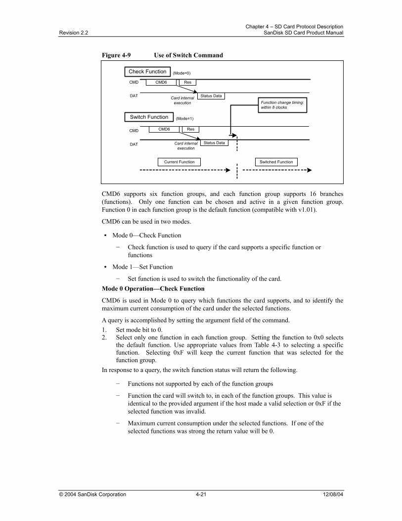
Chapter 4 – SD Card Protocol Description Revision 2.2 SanDisk SD Card Product Manual
© 2004 SanDisk Corporation 4-21 12/08/04
Figure 4-9 Use of Switch Command
CMD6 supports six function groups, and each function group supports 16 branches (functions). Only one function can be chosen and active in a given function group. Function 0 in each function group is the default function (compatible with v1.01).
CMD6 can be used in two modes.
• Mode 0—Check Function
− Check function is used to query if the card supports a specific function or functions
• Mode 1—Set Function
− Set function is used to switch the functionality of the card. Mode 0 Operation—Check Function
CMD6 is used in Mode 0 to query which functions the card supports, and to identify the maximum current consumption of the card under the selected functions.
A query is accomplished by setting the argument field of the command. 1. Set mode bit to 0. 2. Select only one function in each function group. Setting the function to 0x0 selects
the default function. Use appropriate values from Table 4-3 to selecting a specific function. Selecting 0xF will keep the current function that was selected for the function group.
In response to a query, the switch function status will return the following.
− Functions not supported by each of the function groups
− Function the card will switch to, in each of the function groups. This value is identical to the provided argument if the host made a valid selection or 0xF if the selected function was invalid.
− Maximum current consumption under the selected functions. If one of the selected functions was strong the return value will be 0.
Check Function
Switch Function
CMD6 Res
Status Data
Status DataCard internalexecution
Card internalexecution
CMD
DAT
CMD6 ResCMD
DAT
Switched FunctionCurrent Function
(Mode=0)
(Mode=1)
Function change timing:within 8 clocks
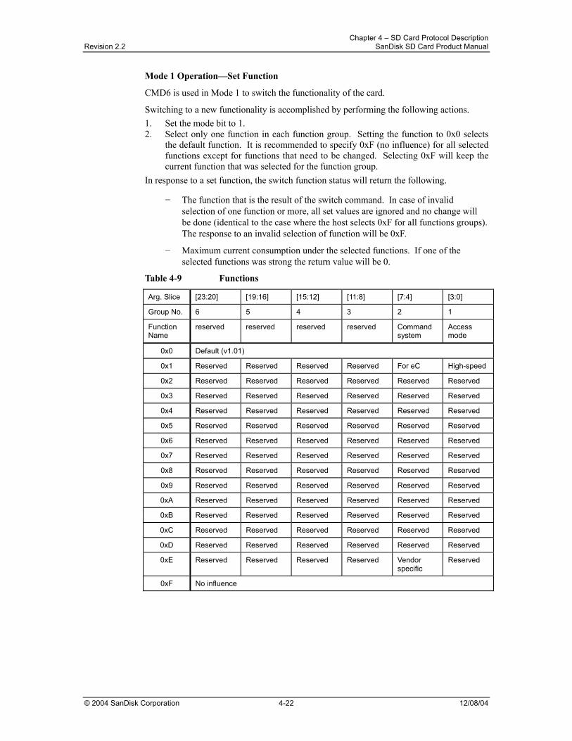
Chapter 4 – SD Card Protocol Description Revision 2.2 SanDisk SD Card Product Manual
© 2004 SanDisk Corporation 4-22 12/08/04
Mode 1 Operation—Set Function
CMD6 is used in Mode 1 to switch the functionality of the card.
Switching to a new functionality is accomplished by performing the following actions. 1. Set the mode bit to 1. 2. Select only one function in each function group. Setting the function to 0x0 selects
the default function. It is recommended to specify 0xF (no influence) for all selected functions except for functions that need to be changed. Selecting 0xF will keep the current function that was selected for the function group.
In response to a set function, the switch function status will return the following.
− The function that is the result of the switch command. In case of invalid selection of one function or more, all set values are ignored and no change will be done (identical to the case where the host selects 0xF for all functions groups). The response to an invalid selection of function will be 0xF.
− Maximum current consumption under the selected functions. If one of the selected functions was strong the return value will be 0.
Table 4-9 Functions
Arg. Slice [23:20] [19:16] [15:12] [11:8] [7:4] [3:0]
Group No. 6 5 4 3 2 1
Function Name
reserved reserved reserved reserved Command system
Access mode
0x0 Default (v1.01)
0x1 Reserved Reserved Reserved Reserved For eC High-speed
0x2 Reserved Reserved Reserved Reserved Reserved Reserved
0x3 Reserved Reserved Reserved Reserved Reserved Reserved
0x4 Reserved Reserved Reserved Reserved Reserved Reserved
0x5 Reserved Reserved Reserved Reserved Reserved Reserved
0x6 Reserved Reserved Reserved Reserved Reserved Reserved
0x7 Reserved Reserved Reserved Reserved Reserved Reserved
0x8 Reserved Reserved Reserved Reserved Reserved Reserved
0x9 Reserved Reserved Reserved Reserved Reserved Reserved
0xA Reserved Reserved Reserved Reserved Reserved Reserved
0xB Reserved Reserved Reserved Reserved Reserved Reserved
0xC Reserved Reserved Reserved Reserved Reserved Reserved
0xD Reserved Reserved Reserved Reserved Reserved Reserved
0xE Reserved Reserved Reserved Reserved Vendor specific
Reserved
0xF No influence
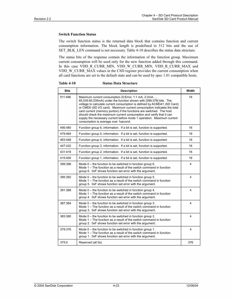
Chapter 4 – SD Card Protocol Description Revision 2.2 SanDisk SD Card Product Manual
© 2004 SanDisk Corporation 4-23 12/08/04
Switch Function Status
The switch function status is the returned data block that contains function and current consumption information. The block length is predefined to 512 bits and the use of SET_BLK_LEN command is not necessary. Table 4-10 describes the status data structure.
The status bits of the response contain the information of the function group. Maximum current consumption will be used only for the new function added through this command. In this case VDD_R_CURR_MIN, VDD_W_CURR_MIN, VDD_R_CURR_MAX and VDD_W_CURR_MAX values in the CSD register provides the current consumption when all card functions are set to the default state and can be used by spec 1.01 compatible hosts.
Table 4-10 Status Data Structure
Bits Description Width
511:496 Maximum current consumption (0:Error, 1:1 mA, 2:2mA…, 65,535:65,535mA) under the function shown with [399:376] bits. The voltage to calculate current consumption is defined by ACMD41 (SD Card) or CMD5 (SD I/O card). Maximum current consumption indicates the total card current (memory portion) if the functions are switched. The host should check the maximum current consumption and verify that it can supply the necessary current before mode 1 operation. Maximum current consumption is average over 1second.
16
495:480 Function group 6, information. If a bit is set, function is supported. 16
479:464 Function group 5, information. If a bit is set, function is supported. 16
463:448 Function group 4, information. If a bit is set, function is supported. 16
447:432 Function group 3, information. If a bit is set, function is supported. 16
431:416 Function group 2, information. If a bit is set, function is supported. 16
415:400 Function group 1, information. If a bit is set, function is supported. 16
399:396 Mode 0 – the function to be switched in function group 6. Mode 1 – The function as a result of the switch command in function group 6. 0xF shows function set error with the argument.
4
395:392 Mode 0 – the function to be switched in function group 5. Mode 1 – The function as a result of the switch command in function group 5. 0xF shows function set error with the argument.
4
391:388 Mode 0 – the function to be switched in function group 4. Mode 1 – The function as a result of the switch command in function group 4. 0xF shows function set error with the argument.
4
387:384 Mode 0 – the function to be switched in function group 3. Mode 1 – The function as a result of the switch command in function group 3. 0xF shows function set error with the argument.
4
383:380 Mode 0 – the function to be switched in function group 2. Mode 1 – The function as a result of the switch command in function group 2. 0xF shows function set error with the argument.
4
379:376 Mode 0 – the function to be switched in function group 1. Mode 1 – The function as a result of the switch command in function group 1. 0xF shows function set error with the argument.
4
375:0 Reserved (all 0s) 376
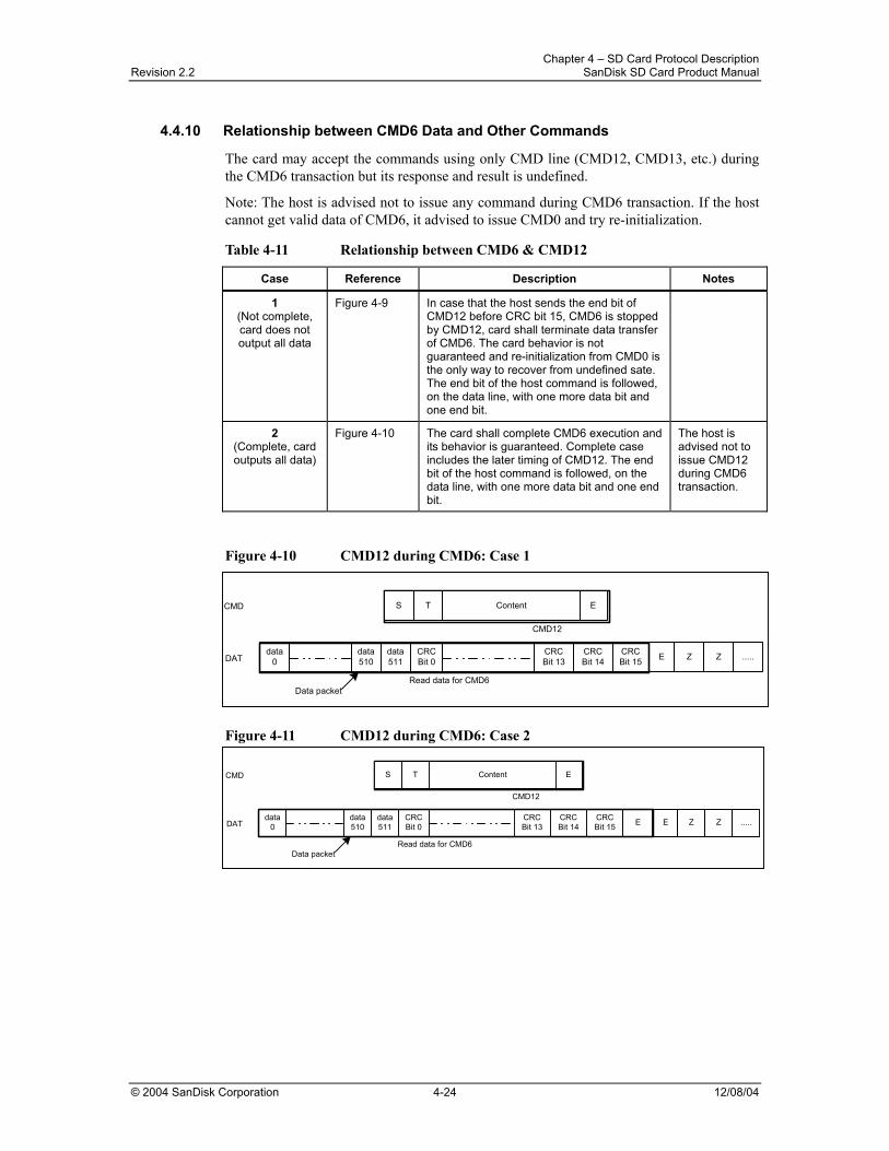
Chapter 4 – SD Card Protocol Description Revision 2.2 SanDisk SD Card Product Manual
© 2004 SanDisk Corporation 4-24 12/08/04
4.4.10 Relationship between CMD6 Data and Other Commands
The card may accept the commands using only CMD line (CMD12, CMD13, etc.) during the CMD6 transaction but its response and result is undefined.
Note: The host is advised not to issue any command during CMD6 transaction. If the host cannot get valid data of CMD6, it advised to issue CMD0 and try re-initialization.
Table 4-11 Relationship between CMD6 & CMD12
Case Reference Description Notes
1 (Not complete, card does not output all data
Figure 4-9 In case that the host sends the end bit of CMD12 before CRC bit 15, CMD6 is stopped by CMD12, card shall terminate data transfer of CMD6. The card behavior is not guaranteed and re-initialization from CMD0 is the only way to recover from undefined sate. The end bit of the host command is followed, on the data line, with one more data bit and one end bit.
2 (Complete, card outputs all data)
Figure 4-10 The card shall complete CMD6 execution and its behavior is guaranteed. Complete case includes the later timing of CMD12. The end bit of the host command is followed, on the data line, with one more data bit and one end bit.
The host is advised not to issue CMD12 during CMD6 transaction.
Figure 4-10 CMD12 during CMD6: Case 1
Figure 4-11 CMD12 during CMD6: Case 2
data0
data510
data511
CRCBit 0
CRCBit 13
CRCBit 14
CRCBit 15 E Z Z .....
T ES Content
CMD12
Read data for CMD6Data packet
CMD
DAT
data0
data510
data511
CRCBit 0
CRCBit 13
CRCBit 14
CRCBit 15 E Z Z .....
T ES Content
CMD12
Read data for CMD6Data packet
CMD
DAT E
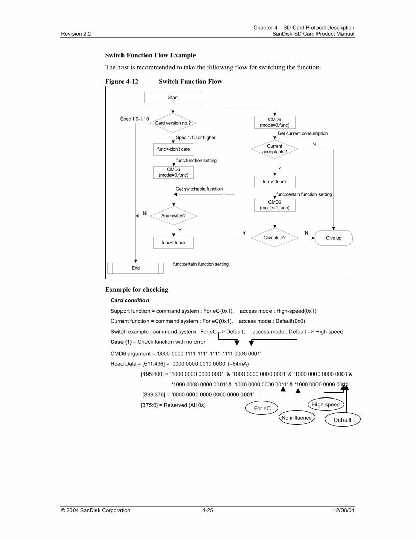
Chapter 4 – SD Card Protocol Description Revision 2.2 SanDisk SD Card Product Manual
© 2004 SanDisk Corporation 4-25 12/08/04
Switch Function Flow Example
The host is recommended to take the following flow for switching the function.
Figure 4-12 Switch Function Flow
Example for checking
Card condition
Support function = command system : For eC(0x1), access mode : High-speed(0x1)
Current function = command system : For eC(0x1), access mode : Default(0x0)
Switch example : command system : For eC => Default, access mode : Default => High-speed
Case (1) – Check function with no error
CMD6 argument = ‘0000 0000 1111 1111 1111 1111 0000 0001’
Read Data = [511:496] = ‘0000 0000 0010 0000’ (=64mA)
[495:400] = ‘1000 0000 0000 0001’ & ‘1000 0000 0000 0001’ & ‘1000 0000 0000 0001’&
‘1000 0000 0000 0001’ & ‘1000 0000 0000 0011’ & ‘1000 0000 0000 0011’
[399:376] = ‘0000 0000 0000 0000 0000 0001’
[375:0] = Reserved (All 0s)
Start
Card version no.?
func<-don't care
CMD6(mode=0,func)
Any switch?
func<-funcx
CMD6(mode=0,func)
Currentacceptable?
func<-funcx
CMD6(mode=1,func)
Complete?
End
Give up
Spec 1.0-1.10
N
N
N
Y Y
Y
Spec 1.10 or higher
func:function setting
Get switchable function
Get current consumption
func:certain function setting
func:certain function setting
For eC
No influence
High-speed
Default
Chapter 4 – SD Card Protocol Description Revision 2.2 SanDisk SD Card Product Manual
© 2004 SanDisk Corporation 4-26 12/08/04
Case (2) – Check function with error
CMD6 argument = ‘0000 0000 1111 1000 1111 0010 0000 0001’
Read Data = [511:496] = ‘0000 0000 0000 0000’ (means error)
[495:400] = ‘1000 0000 0000 0001’ & ‘1000 0000 0000 0001’ & ‘1000 0000 0000 0001’&
‘1000 0000 0000 0001’ & ‘1000 0000 0000 0011’ & ‘1000 0000 0000 0011’
[399:376] = ‘0000 1111 0000 1111 0000 0001’
[375:0] = Reserved (All 0s)
Example for Switching Card condition
Support function = command system : For eC(0x1), access mode : High-speed(0x1)
Current function = command system : For eC(0x1), access mode : Default(0x0)
Switch example : command system : For eC => Default, access mode : Default => High-speed
Case (3) – Switch function with no error
CMD6 argument = ‘1000 0000 1111 1111 1111 1111 0000 0001’
Read Data = [511:496] = ‘0000 0000 0010 0000’ (=64mA)
[495:400] = ‘1000 0000 0000 0001’ & ‘1000 0000 0000 0001’ & ‘1000 0000 0000 0001’&
‘1000 0000 0000 0001’ & ‘1000 0000 0000 0011’ & ‘1000 0000 0000 0011’
[399:376] = ‘0000 0000 0000 0000 0000 0001’
[375:0] = Reserved (All 0s)
Case (4) – Switch function with error
CMD6 argument = ‘1000 0000 1111 1000 1111 0010 0000 0001’
Read Data = [511:496] = ‘0000 0000 0000 0000’ (means error)
[495:400] = ‘1000 0000 0000 0001’ & ‘1000 0000 0000 0001’ & ‘1000 0000 0000 0001’&
‘1000 0000 0000 0001’ & ‘1000 0000 0000 0011’ & ‘1000 0000 0000 0011’
[399:376] = ‘0000 1111 0000 1111 0001 0000’
[375:0] = Reserved (All 0s)
4.4.11 High-speed Mode19 (25MB/sec interface speed)
Although revision 1.01 of the SD Physical Layer Specification supports up to 12.5MB/sec interface speed, the speed of 25MB/sec is necessary to support increasing performance needs of the host and because of growing memory size.
To achieve the 25MB/sec interface speed, the clock rate is increased to 50MHz and CLK/CMD/DAT signal timing and circuit conditions are reconsidered and changed from Physical Layer Specification Version 1.01.
After power-up, the SD Card is in Default Speed mode. Revision 1.10 (and greater) SD cards can be placed in high-speed mode using the Switch Function command (CMD6). The high-speed function belongs to access mode group.
19 High-speed mode is not supported in SPI Mode.
For eC
No influence
High-speed
Default
Error
Error
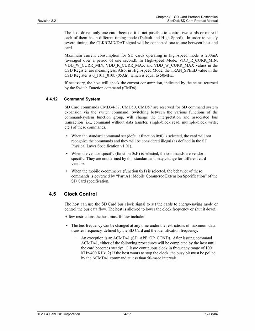
Chapter 4 – SD Card Protocol Description Revision 2.2 SanDisk SD Card Product Manual
© 2004 SanDisk Corporation 4-27 12/08/04
The host drives only one card, because it is not possible to control two cards or more if each of them has a different timing mode (Default and High-Speed). In order to satisfy severe timing, the CLK/CMD/DAT signal will be connected one-to-one between host and card.
Maximum current consumption for SD cards operating in high-speed mode is 200mA (averaged over a period of one second). In High-speed Mode, VDD_R_CURR_MIN, VDD_W_CURR_MIN, VDD_R_CURR_MAX and VDD_W_CURR_MAX values in the CSD Register are meaningless. Also, in High-speed Mode, the TRAN_SPEED value in the CSD Register is 0_1011_010b (05Ah), which is equal to 50MHz.
If necessary, the host will check the current consumption, indicated by the status returned by the Switch Function command (CMD6).
4.4.12 Command System
SD Card commands CMD34-37, CMD50, CMD57 are reserved for SD command system expansion via the switch command. Switching between the various functions of the command-system function group, will change the interpretation and associated bus transaction (i.e., command without data transfer, single-block read, multiple-block write, etc.) of these commands.
• When the standard command set (default function 0x0) is selected, the card will not recognize the commands and they will be considered illegal (as defined in the SD Physical Layer Specification v1.01).
• When the vendor-specific (function 0xE) is selected, the commands are vendor-specific. They are not defined by this standard and may change for different card vendors.
• When the mobile e-commerce (function 0x1) is selected, the behavior of these commands is governed by “Part A1: Mobile Commerce Extension Specification” of the SD Card specification.
4.5 Clock Control
The host can use the SD Card bus clock signal to set the cards to energy-saving mode or control the bus data flow. The host is allowed to lower the clock frequency or shut it down.
A few restrictions the host must follow include:
• The bus frequency can be changed at any time under the restrictions of maximum data transfer frequency, defined by the SD Card and the identification frequency.
− An exception is an ACMD41 (SD_APP_OP_COND). After issuing command ACMD41, either of the following procedures will be completed by the host until the card becomes steady: 1) Issue continuous clock in frequency range of 100 KHz-400 KHz, 2) If the host wants to stop the clock, the busy bit must be polled by the ACMD41 command at less than 50-msec intervals.
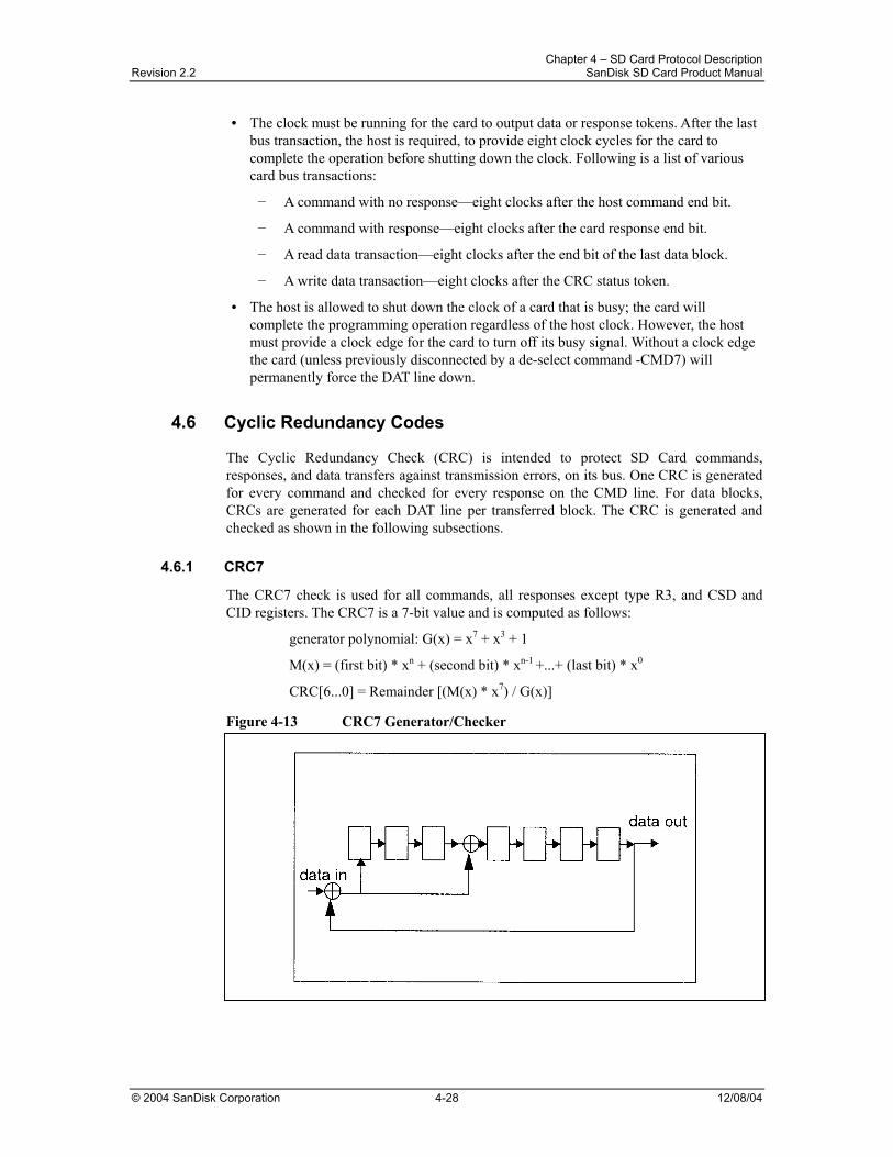
Chapter 4 – SD Card Protocol Description Revision 2.2 SanDisk SD Card Product Manual
© 2004 SanDisk Corporation 4-28 12/08/04
• The clock must be running for the card to output data or response tokens. After the last bus transaction, the host is required, to provide eight clock cycles for the card to complete the operation before shutting down the clock. Following is a list of various card bus transactions:
− A command with no response—eight clocks after the host command end bit.
− A command with response—eight clocks after the card response end bit.
− A read data transaction—eight clocks after the end bit of the last data block.
− A write data transaction—eight clocks after the CRC status token.
• The host is allowed to shut down the clock of a card that is busy; the card will complete the programming operation regardless of the host clock. However, the host must provide a clock edge for the card to turn off its busy signal. Without a clock edge the card (unless previously disconnected by a de-select command -CMD7) will permanently force the DAT line down.
4.6 Cyclic Redundancy Codes
The Cyclic Redundancy Check (CRC) is intended to protect SD Card commands, responses, and data transfers against transmission errors, on its bus. One CRC is generated for every command and checked for every response on the CMD line. For data blocks, CRCs are generated for each DAT line per transferred block. The CRC is generated and checked as shown in the following subsections.
4.6.1 CRC7
The CRC7 check is used for all commands, all responses except type R3, and CSD and CID registers. The CRC7 is a 7-bit value and is computed as follows:
generator polynomial: G(x) = x7 + x3 + 1
M(x) = (first bit) * xn + (second bit) * xn-1 +...+ (last bit) * x0
CRC[6...0] = Remainder [(M(x) * x7) / G(x)]
Figure 4-13 CRC7 Generator/Checker
Chapter 4 – SD Card Protocol Description Revision 2.2 SanDisk SD Card Product Manual
© 2004 SanDisk Corporation 4-29 12/08/04
4.6.2 CRC16
The CRC16 is used for payload protection in block transfer mode when on DAT line is used. The CRC checksum is a 16-bit value and is computed as follows:
generator polynomial: G(x) = x16 + x12 + x5 +1
M(x) = (first bit) * xn + (second bit) * xn-1 +...+ (last bit) * x0
CRC[15...0] = Remainder [(M(x) * x16) / G(x)]
All CRC registers are initialized to zero. The first bit is the first data-bit of the corresponding block. The degree n of the polynomial denotes the number of bits of the data block decreased by one. For example, n = 4,095 for a block length of 512 bytes. The generator polynomial G(x) is a standard CCITT polynomial. The code has a minimal distance d=4 and is used for a payload length of up to 2,048 bytes (n < 16,383). The same CRC16 method is used in single DAT line mode and in wide-bus mode. In wide-bus mode, the CRC16 is done on each line separately.
Figure 4-14 CRC16 Generator/Checker
4.7 Error Conditions
The following sections provide valuable information on error conditions.
4.7.1 CRC and Illegal Commands
CRC-bits protect all commands. If the addressed SD Card CRC check fails, the card does not respond and the command is not executed. The card does not change its state, and the COM_CRC_ERROR bit is set in the Status Register.
Similarly, if an illegal command has been received, an SD Card will not change its state or respond, and will set the ILLEGAL_COMMAND error bit in the Status Register. Only the non-erroneous state branches are shown in the state diagrams (Figure 4-7 and Figure 4-8). Table 4-18 contains a complete state transition description.
Different types of illegal commands include:
• Commands belonging to classes not supported by the SD Card (e.g., I/O command CMD39).
• Commands not allowed in the current state (e.g., CMD2 in Transfer State).
• Commands not defined (e.g., CMD6).
Chapter 4 – SD Card Protocol Description Revision 2.2 SanDisk SD Card Product Manual
© 2004 SanDisk Corporation 4-30 12/08/04
4.7.2 Read, Write and Erase Time-out Conditions
The period after which a time-out condition for read/write/erase operations occurs is (card independent) either 100 times longer than the typical access times for the operations given in Table 4-6 or 100 ms (whichever is lower). The times after which a time-out condition for Write/Erase operations occur are (card independent) either 100 times longer than the typical program times for these operations given below or 250 ms (whichever is lower). A card will complete the command within this time period, or give up and return an error message. If the host does not get any response with the given time-out it should assume the card is not going to respond anymore and try to recover (e.g., reset the card, power cycle, reject). The typical access and program times are defined as shown in Table 4-6.
Table 4-12 Typical Access and Program Time
Operation Definition
Read The read access time is defined as the sum of the two times given by the CSD parameters TAAC and NSAC. These card parameters define the typical delay between the end bit of the read command and the start bit of the data block. This number is card-dependent and should be used by the host to calculate throughput and the maximal frequency for stream read.
Write The R2W_FACTOR field in the CSD is used to calculate the typical block program time obtained by multiplying the read access time by this factor. It applies to all write/erase commands (e.g., SET (CLEAR)_WRITE_PROTECT, PROGRAM_CSD (CID) and the block write commands).
Erase The duration of an erase command will be (order of magnitude) the number of sectors to be erased multiplied by the block write delay.
4.8 Commands
The following sections provide information about commands.
4.8.1 Command Types
There are four kinds of commands defined to control the SD Card bus as shown in Table 4-13.
Table 4-13 Command Definition
Command Abbreviation Definition
Broadcast bc Applicable only if all the CMD lines are connected together in the host. If they are separate, each card will accept it separately in turn.
Broadcast w/Response bcr Response from all cards simultaneously. Because there is not an open-drain mode in the SD Card, this command is used only if all the CMD lines are separate. The command will be accepted and responded to by every card separately.
Addressed point-to-point ac No data transfer on DAT.
Addressed point-to-point data transfer adtc Data transfer on DAT.
The command transmission always starts with the most significant bit (MSB).
Chapter 4 – SD Card Protocol Description Revision 2.2 SanDisk SD Card Product Manual
© 2004 SanDisk Corporation 4-31 12/08/04
4.8.2 Command Format
The command length shown in Figure 4-15 is 48 bits.
Figure 4-15 Format (1.92 µs @ 25 MHz)
0 1 bit 5….bit 0 bit 31….bit 0 bit 6….bit 0 1
start bit host command argument CRC7 end bit
Commands and arguments are listed in Table 4-13.
7-bit CRC Calculation: G(x) = x7+ x3+ 1
M(x) = (start bit)*x39 + (host bit)*x38 +…+ (last bit before CRC)*x0
CRC[6…0] = Remainder[(M(x)*x7)/G(x)]
4.8.3 Command Classes
The command set of the SD Card is divided into several classes (refer to Table 4-15). Each class supports a set of card functions.
The supported Card Command Classes (CCC) is coded as a parameter in the CSD Register data of each card, providing the host with information on how to access the card.
Table 4-15 Card Command Classes
Class 0 1 2 3 4 5 6 7 8 9 10 11
CMD Basic R Block Read
R Block Write
Erase Write Protec
tion
Lock Card
App- Specific
I/O Mode
Switch R
CMD0 +
CMD2 +
CMD3 +
CMD4 +
CMD5 +
CMD620 +
CMD7 +
CMD9 +
CMD10 +
CMD12 +
CMD13 +
CMD15 +
CMD16 + + +
CMD17 +
CMD18 +
CMD24 +
CMD25 +
CMD27 +
20 This command is newly defined in SD Card Physical Description Spec. v1.10
Chapter 4 – SD Card Protocol Description Revision 2.2 SanDisk SD Card Product Manual
© 2004 SanDisk Corporation 4-32 12/08/04
Class 0 1 2 3 4 5 6 7 8 9 10 11
CMD Basic R Block Read
R Block Write
Erase Write Protec
tion
Lock Card
App- Specific
I/O Mode
Switch R
CMD28 +
CMD29 +
CMD30 +
CMD32 +
CMD33 +
CMD3421 to CMD37
+
CMD38 +
CMD42 +
CMD5022 +
CMD52 +
CMD53 +
CMD55 +
CMD56 +
CMD5723 +
ACMD6 +
ACMD13 +
ACMD22 +
ACMD41 +
ACMD42 +
ACMD51 +
R = Reserved
4.8.4 Command Description
All future reserved commands and their responses must be 48 bits long. Responses may not have any response. Table 4-16 details the SD Card bus commands.
Table 4-16 SD Card Bus Command Descriptions
CMD Index Type Argument Resp. Abbreviation Description
Basic Commands (Class 0)
CMD0 bc [31:0] stuff bits
--- GO_IDLE_STATE Reset all cards to Idle State.
CMD1 Reserved
CMD2 bcr [31:0]stuff bits
R2 ALL_SEND_CID Asks all cards to send their CID numbers on the CMD line.
21This command is newly defined in SD Card Physical Description Spec. v1.10 . 22 Ibid. 23 Ibid.
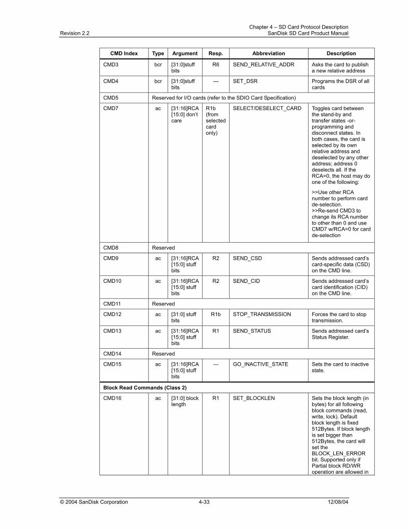
Chapter 4 – SD Card Protocol Description Revision 2.2 SanDisk SD Card Product Manual
© 2004 SanDisk Corporation 4-33 12/08/04
CMD Index Type Argument Resp. Abbreviation Description
CMD3 bcr [31:0]stuff bits
R6 SEND_RELATIVE_ADDR Asks the card to publish a new relative address
CMD4 bcr [31:0]stuff bits
--- SET_DSR Programs the DSR of all cards
CMD5 Reserved for I/O cards (refer to the SDIO Card Specification)
CMD7 ac [31:16]RCA [15:0] don’t care
R1b (from selected card only)
SELECT/DESELECT_CARD Toggles card between the stand-by and transfer states -or- programming and disconnect states. In both cases, the card is selected by its own relative address and deselected by any other address; address 0 deselects all. If the RCA=0, the host may do one of the following:
>>Use other RCA number to perform card de-selection. >>Re-send CMD3 to change its RCA number to other than 0 and use CMD7 w/RCA=0 for card de-selection
CMD8 Reserved
CMD9 ac [31:16]RCA [15:0] stuff bits
R2
SEND_CSD Sends addressed card’s card-specific data (CSD) on the CMD line.
CMD10 ac [31:16]RCA [15:0] stuff bits
R2 SEND_CID Sends addressed card’s card identification (CID) on the CMD line.
CMD11 Reserved
CMD12 ac [31:0] stuff bits
R1b STOP_TRANSMISSION Forces the card to stop transmission.
CMD13 ac [31:16]RCA [15:0] stuff bits
R1 SEND_STATUS Sends addressed card’s Status Register.
CMD14 Reserved
CMD15 ac [31:16]RCA [15:0] stuff bits
--- GO_INACTIVE_STATE Sets the card to inactive state.
Block Read Commands (Class 2)
CMD16 ac [31:0] block length
R1 SET_BLOCKLEN Sets the block length (in bytes) for all following block commands (read, write, lock). Default block length is fixed 512Bytes. If block length is set bigger than 512Bytes, the card will set the BLOCK_LEN_ERROR bit. Supported only if Partial block RD/WR operation are allowed in
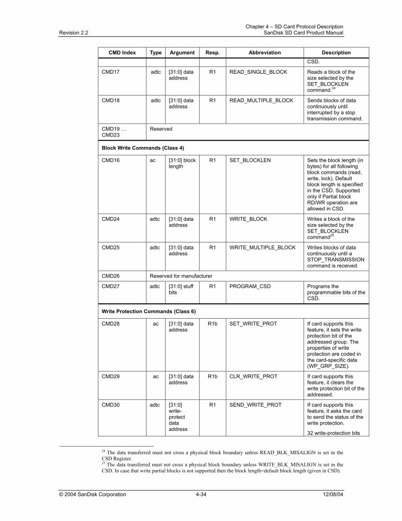
Chapter 4 – SD Card Protocol Description Revision 2.2 SanDisk SD Card Product Manual
© 2004 SanDisk Corporation 4-34 12/08/04
CMD Index Type Argument Resp. Abbreviation Description CSD.
CMD17 adtc [31:0] data address
R1 READ_SINGLE_BLOCK Reads a block of the size selected by the SET_BLOCKLEN command.24
CMD18 adtc [31:0] data address
R1 READ_MULTIPLE_BLOCK Sends blocks of data continuously until interrupted by a stop transmission command.
CMD19 … CMD23
Reserved
Block Write Commands (Class 4)
CMD16 ac [31:0] block length
R1 SET_BLOCKLEN Sets the block length (in bytes) for all following block commands (read, write, lock). Default block length is specified in the CSD. Supported only if Partial block RD/WR operation are allowed in CSD.
CMD24 adtc [31:0] data address
R1 WRITE_BLOCK Writes a block of the size selected by the SET_BLOCKLEN command25
CMD25 adtc [31:0] data address
R1 WRITE_MULTIPLE_BLOCK Writes blocks of data continuously until a STOP_TRANSMISSION command is received.
CMD26 Reserved for manufacturer
CMD27 adtc [31:0] stuff bits
R1 PROGRAM_CSD Programs the programmable bits of the CSD.
Write Protection Commands (Class 6)
CMD28 ac [31:0] data address
R1b SET_WRITE_PROT If card supports this feature, it sets the write protection bit of the addressed group. The properties of write protection are coded in the card-specific data (WP_GRP_SIZE).
CMD29 ac [31:0] data address
R1b CLR_WRITE_PROT If card supports this feature, it clears the write protection bit of the addressed.
CMD30 adtc [31:0] write- protect data address
R1 SEND_WRITE_PROT If card supports this feature, it asks the card to send the status of the write protection.
32 write-protection bits
24 The data transferred must not cross a physical block boundary unless READ_BLK_MISALIGN is set in the CSD Register. 25 The data transferred must not cross a physical block boundary unless WRITE_BLK_MISALIGN is set in the CSD. In case that write partial blocks is not supported then the block length=default block length (given in CSD).
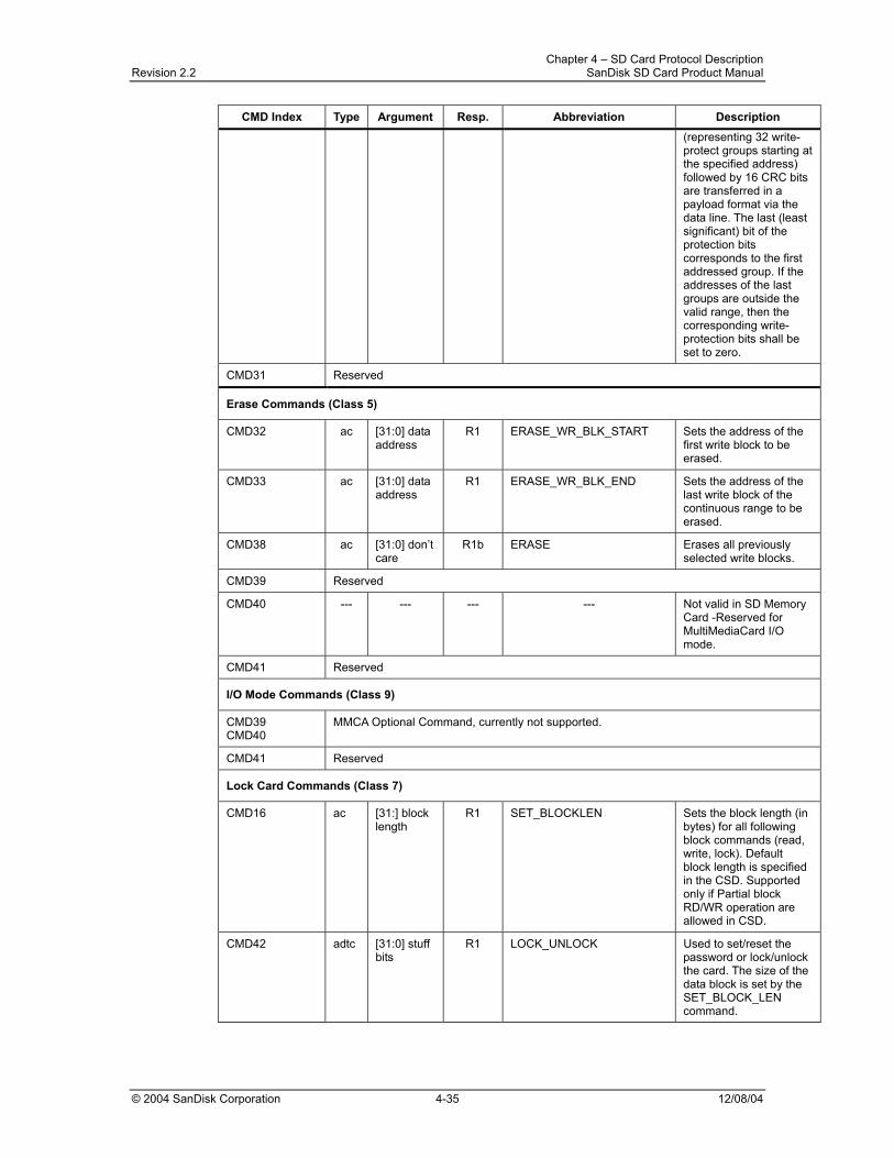
Chapter 4 – SD Card Protocol Description Revision 2.2 SanDisk SD Card Product Manual
© 2004 SanDisk Corporation 4-35 12/08/04
CMD Index Type Argument Resp. Abbreviation Description (representing 32 write- protect groups starting at the specified address) followed by 16 CRC bits are transferred in a payload format via the data line. The last (least significant) bit of the protection bits corresponds to the first addressed group. If the addresses of the last groups are outside the valid range, then the corresponding write- protection bits shall be set to zero.
CMD31 Reserved
Erase Commands (Class 5)
CMD32 ac [31:0] data address
R1 ERASE_WR_BLK_START Sets the address of the first write block to be erased.
CMD33 ac [31:0] data address
R1 ERASE_WR_BLK_END Sets the address of the last write block of the continuous range to be erased.
CMD38 ac [31:0] don’t care
R1b ERASE Erases all previously selected write blocks.
CMD39 Reserved
CMD40 --- --- --- --- Not valid in SD Memory Card -Reserved for MultiMediaCard I/O mode.
CMD41 Reserved
I/O Mode Commands (Class 9)
CMD39 CMD40
MMCA Optional Command, currently not supported.
CMD41 Reserved
Lock Card Commands (Class 7)
CMD16 ac [31:] block length
R1 SET_BLOCKLEN Sets the block length (in bytes) for all following block commands (read, write, lock). Default block length is specified in the CSD. Supported only if Partial block RD/WR operation are allowed in CSD.
CMD42 adtc [31:0] stuff bits
R1 LOCK_UNLOCK Used to set/reset the password or lock/unlock the card. The size of the data block is set by the SET_BLOCK_LEN command.
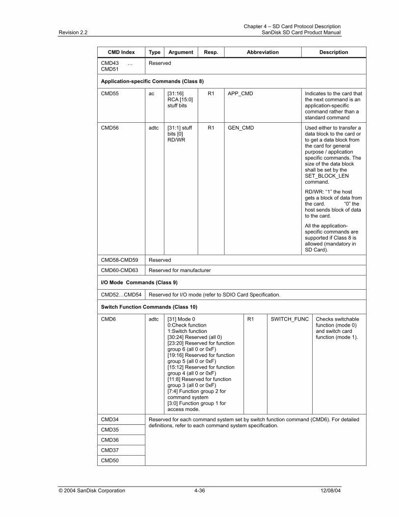
Chapter 4 – SD Card Protocol Description Revision 2.2 SanDisk SD Card Product Manual
© 2004 SanDisk Corporation 4-36 12/08/04
CMD Index Type Argument Resp. Abbreviation Description
CMD43 … CMD51
Reserved
Application-specific Commands (Class 8)
CMD55 ac [31:16] RCA [15:0] stuff bits
R1 APP_CMD Indicates to the card that the next command is an application-specific command rather than a standard command
CMD56 adtc [31:1] stuff bits [0] RD/WR
R1 GEN_CMD Used either to transfer a data block to the card or to get a data block from the card for general purpose / application specific commands. The size of the data block shall be set by the SET_BLOCK_LEN command.
RD/WR: “1” the host gets a block of data from the card. “0” the host sends block of data to the card.
All the application-specific commands are supported if Class 8 is allowed (mandatory in SD Card).
CMD58-CMD59 Reserved
CMD60-CMD63 Reserved for manufacturer
I/O Mode Commands (Class 9)
CMD52…CMD54 Reserved for I/O mode (refer to SDIO Card Specification.
Switch Function Commands (Class 10)
CMD6 adtc [31] Mode 0 0:Check function 1:Switch function [30:24] Reserved (all 0) [23:20] Reserved for function group 6 (all 0 or 0xF) [19:16] Reserved for function group 5 (all 0 or 0xF) [15:12] Reserved for function group 4 (all 0 or 0xF) [11:8] Reserved for function group 3 (all 0 or 0xF) [7:4] Function group 2 for command system [3:0] Function group 1 for access mode.
R1 SWITCH_FUNC Checks switchable function (mode 0) and switch card function (mode 1).
CMD34
CMD35
CMD36
CMD37
CMD50
Reserved for each command system set by switch function command (CMD6). For detailed definitions, refer to each command system specification.
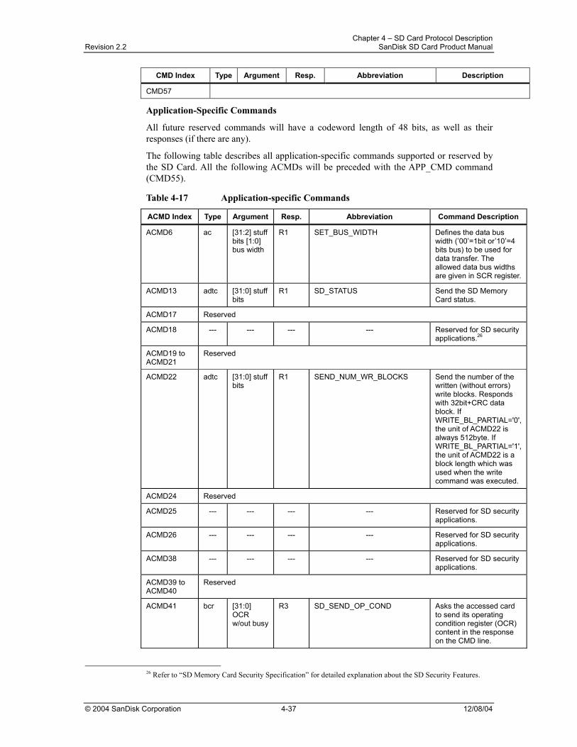
Chapter 4 – SD Card Protocol Description Revision 2.2 SanDisk SD Card Product Manual
© 2004 SanDisk Corporation 4-37 12/08/04
CMD Index Type Argument Resp. Abbreviation Description
CMD57
Application-Specific Commands
All future reserved commands will have a codeword length of 48 bits, as well as their responses (if there are any).
The following table describes all application-specific commands supported or reserved by the SD Card. All the following ACMDs will be preceded with the APP_CMD command (CMD55).
Table 4-17 Application-specific Commands
ACMD Index Type Argument Resp. Abbreviation Command Description
ACMD6 ac [31:2] stuff bits [1:0] bus width
R1 SET_BUS_WIDTH Defines the data bus width (’00’=1bit or’10’=4 bits bus) to be used for data transfer. The allowed data bus widths are given in SCR register.
ACMD13 adtc [31:0] stuff bits
R1 SD_STATUS Send the SD Memory Card status.
ACMD17 Reserved
ACMD18 --- --- --- --- Reserved for SD security applications.26
ACMD19 to ACMD21
Reserved
ACMD22 adtc [31:0] stuff bits
R1 SEND_NUM_WR_BLOCKS Send the number of the written (without errors) write blocks. Responds with 32bit+CRC data block. If WRITE_BL_PARTIAL='0', the unit of ACMD22 is always 512byte. If WRITE_BL_PARTIAL='1', the unit of ACMD22 is a block length which was used when the write command was executed.
ACMD24 Reserved
ACMD25 --- --- --- --- Reserved for SD security applications.
ACMD26 --- --- --- --- Reserved for SD security applications.
ACMD38 --- --- --- --- Reserved for SD security applications.
ACMD39 to ACMD40
Reserved
ACMD41 bcr [31:0] OCR w/out busy
R3 SD_SEND_OP_COND Asks the accessed card to send its operating condition register (OCR) content in the response on the CMD line.
26 Refer to “SD Memory Card Security Specification” for detailed explanation about the SD Security Features.
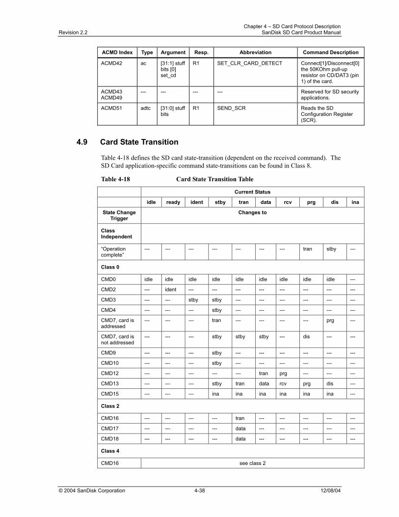
Chapter 4 – SD Card Protocol Description Revision 2.2 SanDisk SD Card Product Manual
© 2004 SanDisk Corporation 4-38 12/08/04
ACMD Index Type Argument Resp. Abbreviation Command Description
ACMD42 ac [31:1] stuff bits [0] set_cd
R1 SET_CLR_CARD_DETECT Connect[1]/Disconnect[0] the 50KOhm pull-up resistor on CD/DAT3 (pin 1) of the card.
ACMD43 ACMD49
--- --- --- --- Reserved for SD security applications.
ACMD51 adtc [31:0] stuff bits
R1 SEND_SCR Reads the SD Configuration Register (SCR).
4.9 Card State Transition
Table 4-18 defines the SD card state-transition (dependent on the received command). The SD Card application-specific command state-transitions can be found in Class 8.
Table 4-18 Card State Transition Table
Current Status
idle ready ident stby tran data rcv prg dis ina
State Change Trigger
Changes to
Class Independent
“Operation complete”
--- --- --- --- --- --- --- tran stby ---
Class 0
CMD0 idle idle idle idle idle idle idle idle idle ---
CMD2 --- ident --- --- --- --- --- --- --- ---
CMD3 --- --- stby stby --- --- --- --- --- ---
CMD4 --- --- --- stby --- --- --- --- --- ---
CMD7, card is addressed
--- --- --- tran --- --- --- --- prg ---
CMD7, card is not addressed
--- --- --- stby stby stby --- dis --- ---
CMD9 --- --- --- stby --- --- --- --- --- ---
CMD10 --- --- --- stby --- --- --- --- --- ---
CMD12 --- --- --- --- --- tran prg --- --- ---
CMD13 --- --- --- stby tran data rcv prg dis ---
CMD15 --- --- --- ina ina ina ina ina ina ---
Class 2
CMD16 --- --- --- --- tran --- --- --- --- ---
CMD17 --- --- --- --- data --- --- --- --- ---
CMD18 --- --- --- --- data --- --- --- --- ---
Class 4
CMD16 see class 2
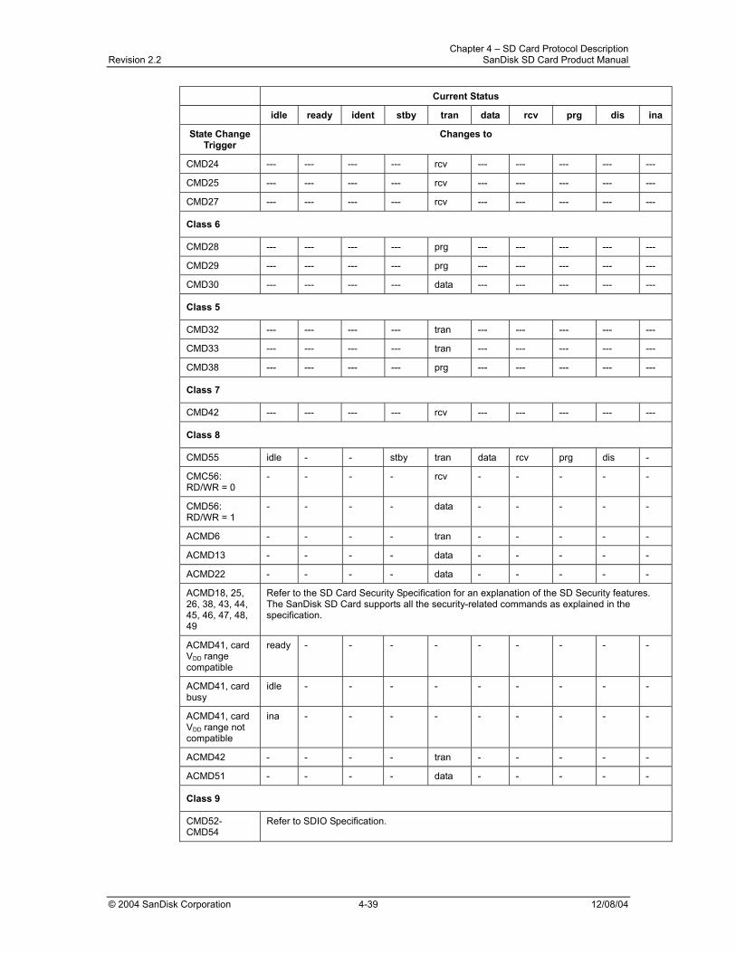
Chapter 4 – SD Card Protocol Description Revision 2.2 SanDisk SD Card Product Manual
© 2004 SanDisk Corporation 4-39 12/08/04
Current Status
idle ready ident stby tran data rcv prg dis ina
State Change Trigger
Changes to
CMD24 --- --- --- --- rcv --- --- --- --- ---
CMD25 --- --- --- --- rcv --- --- --- --- ---
CMD27 --- --- --- --- rcv --- --- --- --- ---
Class 6
CMD28 --- --- --- --- prg --- --- --- --- ---
CMD29 --- --- --- --- prg --- --- --- --- ---
CMD30 --- --- --- --- data --- --- --- --- ---
Class 5
CMD32 --- --- --- --- tran --- --- --- --- ---
CMD33 --- --- --- --- tran --- --- --- --- ---
CMD38 --- --- --- --- prg --- --- --- --- ---
Class 7
CMD42 --- --- --- --- rcv --- --- --- --- ---
Class 8
CMD55 idle - - stby tran data rcv prg dis -
CMC56: RD/WR = 0
- - - - rcv - - - - -
CMD56: RD/WR = 1
- - - - data - - - - -
ACMD6 - - - - tran - - - - -
ACMD13 - - - - data - - - - -
ACMD22 - - - - data - - - - -
ACMD18, 25, 26, 38, 43, 44, 45, 46, 47, 48, 49
Refer to the SD Card Security Specification for an explanation of the SD Security features. The SanDisk SD Card supports all the security-related commands as explained in the specification.
ACMD41, card VDD range compatible
ready - - - - - - - - -
ACMD41, card busy
idle - - - - - - - - -
ACMD41, card VDD range not compatible
ina - - - - - - - - -
ACMD42 - - - - tran - - - - -
ACMD51 - - - - data - - - - -
Class 9
CMD52-CMD54
Refer to SDIO Specification.
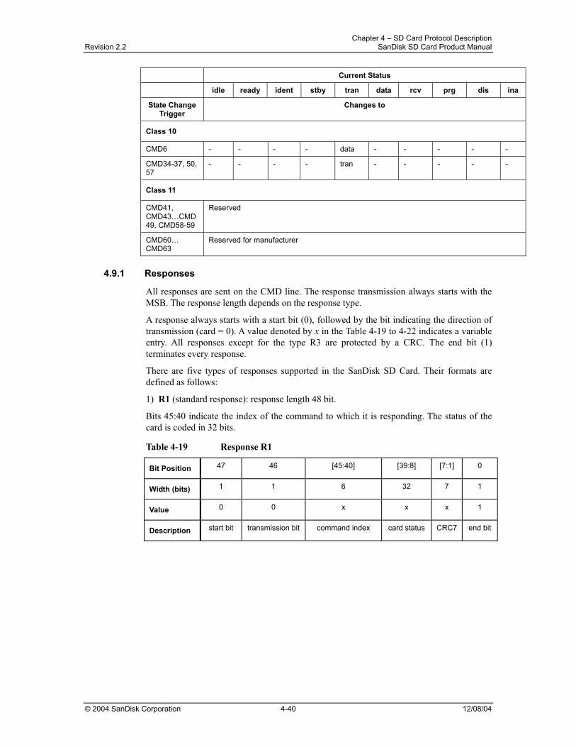
Chapter 4 – SD Card Protocol Description Revision 2.2 SanDisk SD Card Product Manual
© 2004 SanDisk Corporation 4-40 12/08/04
Current Status
idle ready ident stby tran data rcv prg dis ina
State Change Trigger
Changes to
Class 10
CMD6 - - - - data - - - - -
CMD34-37, 50, 57
- - - - tran - - - - -
Class 11
CMD41, CMD43…CMD49, CMD58-59
Reserved
CMD60… CMD63
Reserved for manufacturer
4.9.1 Responses
All responses are sent on the CMD line. The response transmission always starts with the MSB. The response length depends on the response type.
A response always starts with a start bit (0), followed by the bit indicating the direction of transmission (card = 0). A value denoted by x in the Table 4-19 to 4-22 indicates a variable entry. All responses except for the type R3 are protected by a CRC. The end bit (1) terminates every response.
There are five types of responses supported in the SanDisk SD Card. Their formats are defined as follows:
1) R1 (standard response): response length 48 bit.
Bits 45:40 indicate the index of the command to which it is responding. The status of the card is coded in 32 bits.
Table 4-19 Response R1
Bit Position 47 46 [45:40] [39:8] [7:1] 0
Width (bits) 1 1 6 32 7 1
Value 0 0 x x x 1
Description start bit transmission bit command index card status CRC7 end bit
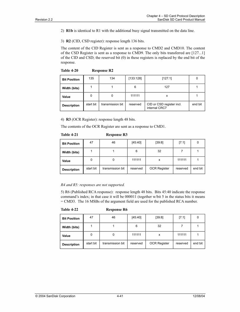
Chapter 4 – SD Card Protocol Description Revision 2.2 SanDisk SD Card Product Manual
© 2004 SanDisk Corporation 4-41 12/08/04
2) R1b is identical to R1 with the additional busy signal transmitted on the data line. 3) R2 (CID, CSD register): response length 136 bits.
The content of the CID Register is sent as a response to CMD2 and CMD10. The content of the CSD Register is sent as a response to CMD9. The only bits transferred are [127...1] of the CID and CSD; the reserved bit (0) in these registers is replaced by the end bit of the response.
Table 4-20 Response R2
Bit Position 135 134 [133:128] [127:1] 0
Width (bits) 1 1 6 127 1
Value 0 0 111111 x 1
Description start bit transmission bit reserved CID or CSD register incl. internal CRC7
end bit
4) R3 (OCR Register): response length 48 bits.
The contents of the OCR Register are sent as a response to CMD1.
Table 4-21 Response R3
Bit Position 47 46 [45:40] [39:8] [7:1] 0
Width (bits) 1 1 6 32 7 1
Value 0 0 111111 x 111111 1
Description start bit transmission bit reserved OCR Register reserved end bit
R4 and R5: responses are not supported.
5) R6 (Published RCA response): response length 48 bits. Bits 45:40 indicate the response command’s index; in that case it will be 000011 (together w/bit 5 in the status bits it means = CMD3. The 16 MSBs of the argument field are used for the published RCA number.
Table 4-22 Response R6
Bit Position 47 46 [45:40] [39:8] [7:1] 0
Width (bits) 1 1 6 32 7 1
Value 0 0 111111 x 111111 1
Description start bit transmission bit reserved OCR Register reserved end bit
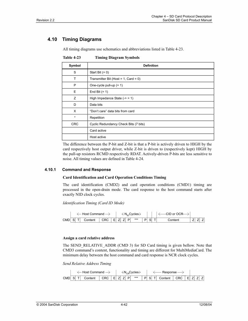
Chapter 4 – SD Card Protocol Description Revision 2.2 SanDisk SD Card Product Manual
© 2004 SanDisk Corporation 4-42 12/08/04
4.10 Timing Diagrams
All timing diagrams use schematics and abbreviations listed in Table 4-23.
Table 4-23 Timing Diagram Symbols
Symbol Definition
S Start Bit (= 0)
T Transmitter Bit (Host = 1, Card = 0)
P One-cycle pull-up (= 1)
E End Bit (= 1)
Z High Impedance State (-> = 1)
D Data bits
X “Don’t care” data bits from card
* Repetition
CRC Cyclic Redundancy Check Bits (7 bits)
Card active
Host active
The difference between the P-bit and Z-bit is that a P-bit is actively driven to HIGH by the card respectively host output driver, while Z-bit is driven to (respectively kept) HIGH by the pull-up resistors RCMD respectively RDAT. Actively-driven P-bits are less sensitive to noise. All timing values are defined in Table 4-24.
4.10.1 Command and Response
Card Identification and Card Operation Conditions Timing
The card identification (CMD2) and card operation conditions (CMD1) timing are processed in the open-drain mode. The card response to the host command starts after exactly NID clock cycles.
Identification Timing (Card ID Mode)
Assign a card relative address
The SEND_RELATIVE_ADDR (CMD 3) for SD Card timing is given bellow. Note that CMD3 command’s content, functionality and timing are different for MultiMediaCard. The minimum delay between the host command and card response is NCR clock cycles.
Send Relative Address Timing
CMD S T Content E Z *** P S T Z Z Z
Host Command NCR
CRC
ResponseCycles
Content CRC ZEZ P
CMD S T Content E Z *** P S T Z Z
Host Command NID
CRC
CID or OCRCycles
Content ZZ P
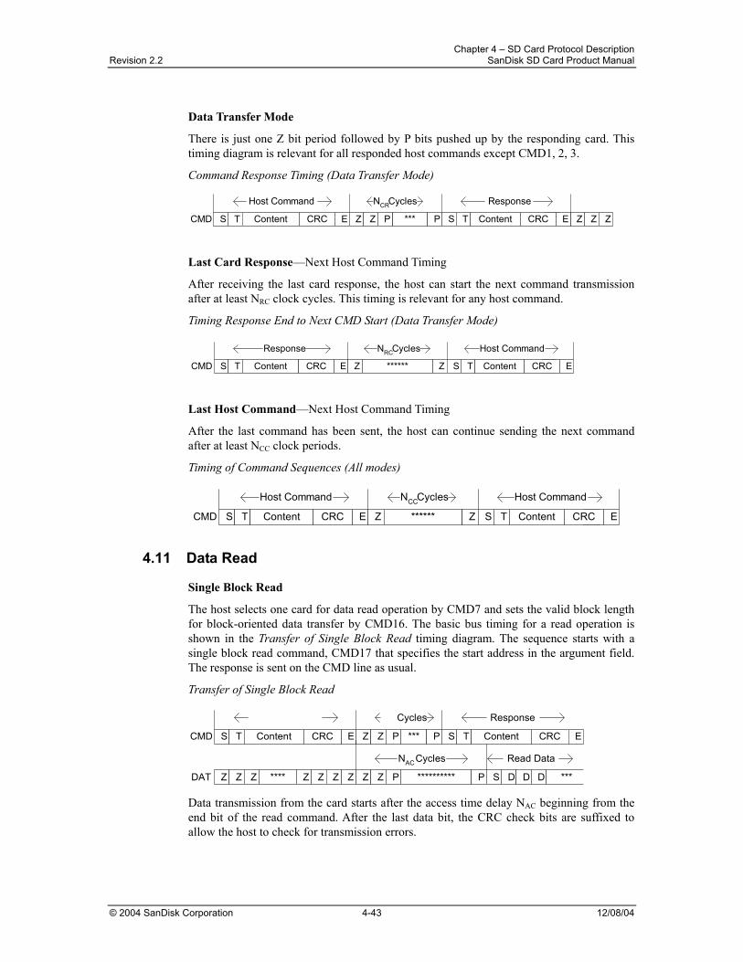
Chapter 4 – SD Card Protocol Description Revision 2.2 SanDisk SD Card Product Manual
© 2004 SanDisk Corporation 4-43 12/08/04
Data Transfer Mode
There is just one Z bit period followed by P bits pushed up by the responding card. This timing diagram is relevant for all responded host commands except CMD1, 2, 3.
Command Response Timing (Data Transfer Mode)
Last Card Response—Next Host Command Timing
After receiving the last card response, the host can start the next command transmission after at least NRC clock cycles. This timing is relevant for any host command.
Timing Response End to Next CMD Start (Data Transfer Mode)
Last Host Command—Next Host Command Timing
After the last command has been sent, the host can continue sending the next command after at least NCC clock periods.
Timing of Command Sequences (All modes)
4.11 Data Read
Single Block Read
The host selects one card for data read operation by CMD7 and sets the valid block length for block-oriented data transfer by CMD16. The basic bus timing for a read operation is shown in the Transfer of Single Block Read timing diagram. The sequence starts with a single block read command, CMD17 that specifies the start address in the argument field. The response is sent on the CMD line as usual.
Transfer of Single Block Read
Data transmission from the card starts after the access time delay NAC beginning from the end bit of the read command. After the last data bit, the CRC check bits are suffixed to allow the host to check for transmission errors.
CMD S T Content E Z ****** Z S T Z
Host Command NCC
CRC
Host CommandCycles
Content CRC E
CMD S T Content E Z *** P S TCRC
ResponseCycles
Content CRC EZ P
DAT Z Z **** Z Z **********Z P S D
NAC Read DataCycles
DZ Z Z Z P D ***
CMD S T Content E Z *** P S T Z Z Z
Host Command NCR
CRC
ResponseCycles
Content CRC ZEZ P
CMD S T Content E Z ****** Z S T Z
Response NRC
CRC
Host CommandCycles
Content CRC E
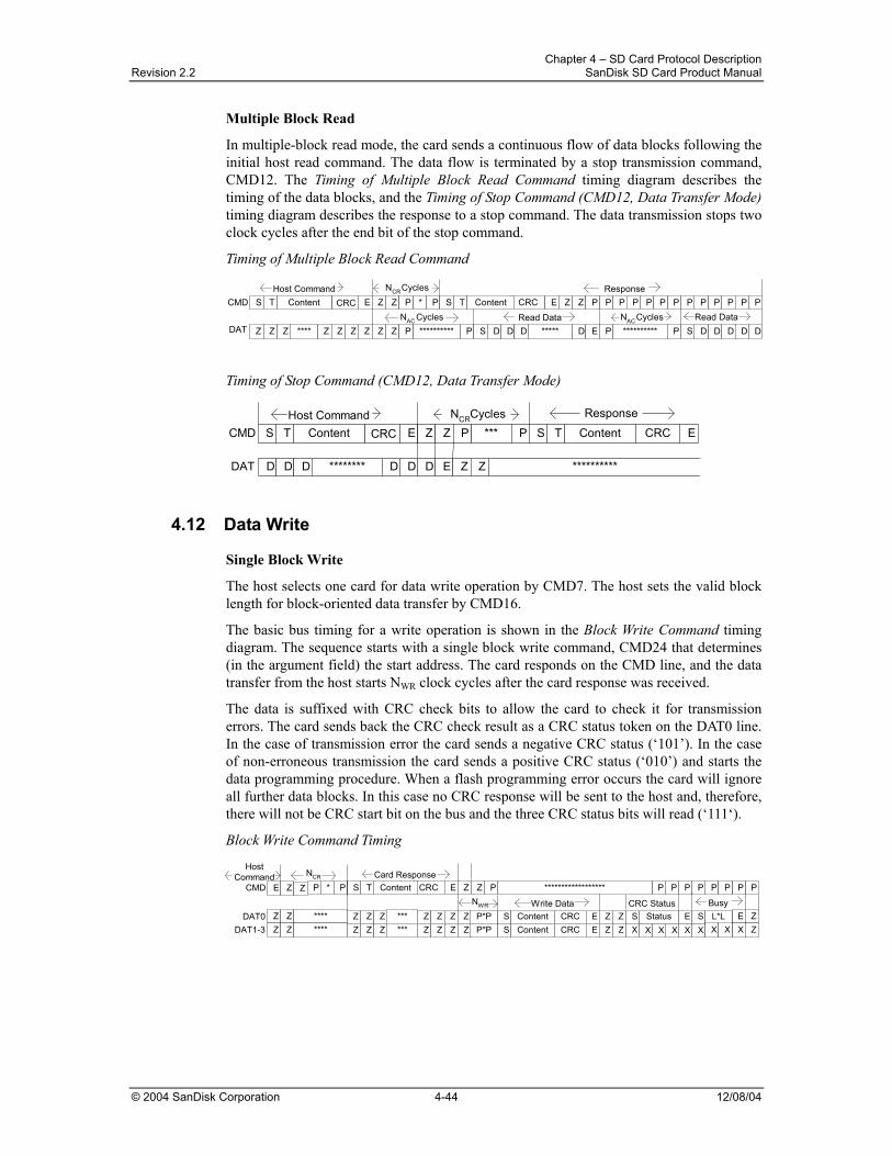
Chapter 4 – SD Card Protocol Description Revision 2.2 SanDisk SD Card Product Manual
© 2004 SanDisk Corporation 4-44 12/08/04
Multiple Block Read
In multiple-block read mode, the card sends a continuous flow of data blocks following the initial host read command. The data flow is terminated by a stop transmission command, CMD12. The Timing of Multiple Block Read Command timing diagram describes the timing of the data blocks, and the Timing of Stop Command (CMD12, Data Transfer Mode) timing diagram describes the response to a stop command. The data transmission stops two clock cycles after the end bit of the stop command.
Timing of Multiple Block Read Command
Timing of Stop Command (CMD12, Data Transfer Mode)
4.12 Data Write
Single Block Write
The host selects one card for data write operation by CMD7. The host sets the valid block length for block-oriented data transfer by CMD16.
The basic bus timing for a write operation is shown in the Block Write Command timing diagram. The sequence starts with a single block write command, CMD24 that determines (in the argument field) the start address. The card responds on the CMD line, and the data transfer from the host starts NWR clock cycles after the card response was received.
The data is suffixed with CRC check bits to allow the card to check it for transmission errors. The card sends back the CRC check result as a CRC status token on the DAT0 line. In the case of transmission error the card sends a negative CRC status (‘101’). In the case of non-erroneous transmission the card sends a positive CRC status (‘010’) and starts the data programming procedure. When a flash programming error occurs the card will ignore all further data blocks. In this case no CRC response will be sent to the host and, therefore, there will not be CRC start bit on the bus and the three CRC status bits will read (‘111‘).
Block Write Command Timing
CMD S T E Z * P S TResponse
CRC EZ P
DAT Z Z **** Z Z **********Z P S D DZ Z Z Z P D *****
Z PZ P P PP P PPP P P P PNCRCycles
D E P ********** P DDS D D D
Content CRC ContentHost Command
NACCyclesNAC Cycles Read Data Read Data
CMD S T E Z *** P S TZ PNCRCycles
Content CRCHost Command
Content ECRC
D D D ******** D D D E Z Z **********
Response
DAT
CMD E Z
Busy
CRC E Z Z P P PP P PPP PNCR Card Response
Content
HostCommand
Write Data CRC Status
Z P * P S ******************T
DAT0 Z Z **** SZ Z Z E S E Z***Z Z Z Z P*P Content CRC E Z Z S Status L*LDAT1-3 Z Z **** SZ Z Z X X X Z***Z Z Z Z P*P Content CRC E Z Z X X X X X X
NWR
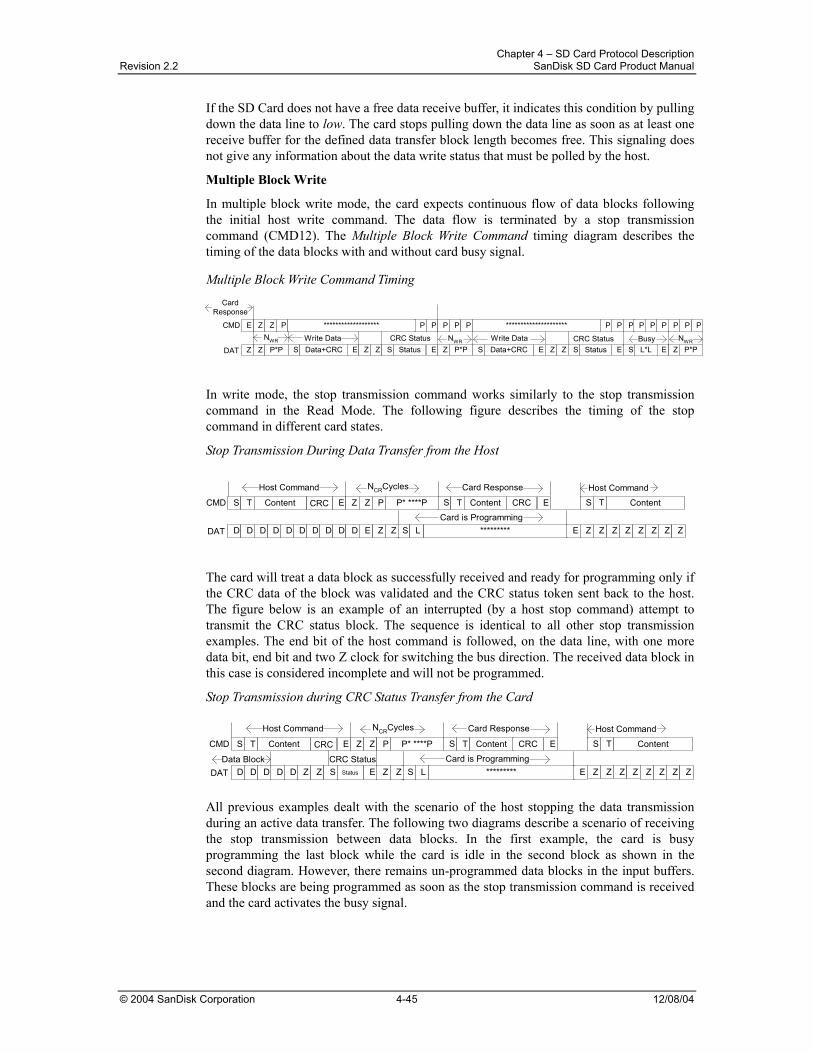
Chapter 4 – SD Card Protocol Description Revision 2.2 SanDisk SD Card Product Manual
© 2004 SanDisk Corporation 4-45 12/08/04
If the SD Card does not have a free data receive buffer, it indicates this condition by pulling down the data line to low. The card stops pulling down the data line as soon as at least one receive buffer for the defined data transfer block length becomes free. This signaling does not give any information about the data write status that must be polled by the host.
Multiple Block Write
In multiple block write mode, the card expects continuous flow of data blocks following the initial host write command. The data flow is terminated by a stop transmission command (CMD12). The Multiple Block Write Command timing diagram describes the timing of the data blocks with and without card busy signal.
Multiple Block Write Command Timing
In write mode, the stop transmission command works similarly to the stop transmission command in the Read Mode. The following figure describes the timing of the stop command in different card states.
Stop Transmission During Data Transfer from the Host
The card will treat a data block as successfully received and ready for programming only if the CRC data of the block was validated and the CRC status token sent back to the host. The figure below is an example of an interrupted (by a host stop command) attempt to transmit the CRC status block. The sequence is identical to all other stop transmission examples. The end bit of the host command is followed, on the data line, with one more data bit, end bit and two Z clock for switching the bus direction. The received data block in this case is considered incomplete and will not be programmed.
Stop Transmission during CRC Status Transfer from the Card
All previous examples dealt with the scenario of the host stopping the data transmission during an active data transfer. The following two diagrams describe a scenario of receiving the stop transmission between data blocks. In the first example, the card is busy programming the last block while the card is idle in the second block as shown in the second diagram. However, there remains un-programmed data blocks in the input buffers. These blocks are being programmed as soon as the stop transmission command is received and the card activates the busy signal.
CMD E Z
BusyDAT Z Z P*P S ZE
P P PP P PPP PNWR
E S
CardResponse
NWRWrite Data CRC Status
Z P *******************
E Z SP*PData+CRC E Z Z S Status L*L
P P P P *********************
Data+CRC E Z Z S Status
P
P*PWrite Data CRC Status NWR
CMD S T
DAT ZZ
E S T
Z Z
Card Response
Z
Content
*********
Z Z P S
E Z Z
E
Card is Programming
Host Command
Content P* ****P T Content CRCCRC
Z
Host Command NCRCycles
D D D D D Z SD D D D D E LZ
CMD S T
DAT ZZ
E S T
Z Z
Card Response
Z
Content
*********
Z Z P S
E Z Z
E
Card is Programming
Host Command
Content P* ****P T Content CRCCRC
Z
Host Command NCRCycles
D D D D Z Z SD Z S E LZData Block
Status
CRC Status
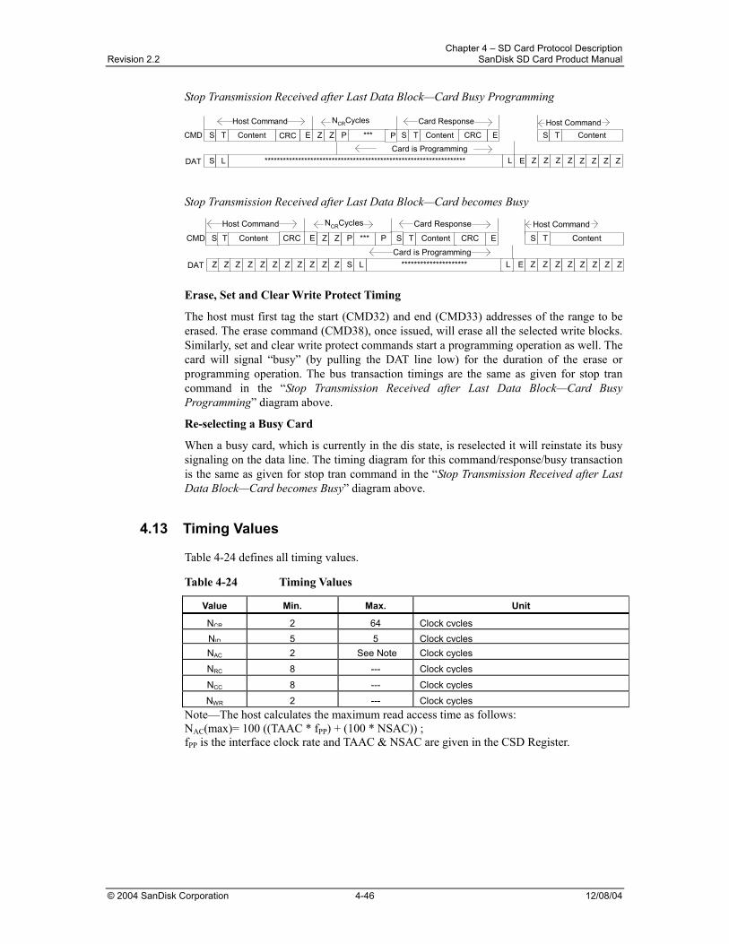
Chapter 4 – SD Card Protocol Description Revision 2.2 SanDisk SD Card Product Manual
© 2004 SanDisk Corporation 4-46 12/08/04
Stop Transmission Received after Last Data Block—Card Busy Programming
Stop Transmission Received after Last Data Block—Card becomes Busy
Erase, Set and Clear Write Protect Timing
The host must first tag the start (CMD32) and end (CMD33) addresses of the range to be erased. The erase command (CMD38), once issued, will erase all the selected write blocks. Similarly, set and clear write protect commands start a programming operation as well. The card will signal “busy” (by pulling the DAT line low) for the duration of the erase or programming operation. The bus transaction timings are the same as given for stop tran command in the “Stop Transmission Received after Last Data Block—Card Busy Programming” diagram above.
Re-selecting a Busy Card
When a busy card, which is currently in the dis state, is reselected it will reinstate its busy signaling on the data line. The timing diagram for this command/response/busy transaction is the same as given for stop tran command in the “Stop Transmission Received after Last Data Block—Card becomes Busy” diagram above.
4.13 Timing Values
Table 4-24 defines all timing values.
Table 4-24 Timing Values
Value Min. Max. Unit
NCR 2 64 Clock cyclesNID 5 5 Clock cyclesNAC 2 See Note Clock cycles
NRC 8 --- Clock cycles
NCC 8 --- Clock cycles
NWR 2 --- Clock cyclesNote—The host calculates the maximum read access time as follows: NAC(max)= 100 ((TAAC * fPP) + (100 * NSAC)) ; fPP is the interface clock rate and TAAC & NSAC are given in the CSD Register.
CMD
DAT
S T
ZZ
E S T
Z Z
Card Response
Z
Content
******************************************************************
Z Z P S
E Z Z
E
Card is Programming
Host CommandContent *** T Content CRCCRC
Z
Host Command NCRCycles
S L L
P
CMD S T
DAT ZZ
S T
Z Z
Card Response
Z
Content
*********************
Z Z S
E Z Z
E
Card is Programming
Host Command
Content P T Content CRCCRC
Z
Host Command NCRCycles
Z Z Z Z Z Z SZ Z Z LZ Z L
***E P
Chapter 5 – SPI Protocol Revision 2.2 SD Card Product Manual
© 2004 SanDisk Corporation 5-1 12/08/04
5 SPI Protocol
5.1 SPI Bus Protocol Although the SanDisk SD Card channel is based on command and data bit-streams initiated by a start bit and terminated by a stop bit, the SPI channel is byte-oriented. Every command or data block is built of eight-bit bytes and byte aligned (multiples of eight clocks) to the CS signal.
Similar to the SD Bus protocol, the SPI messages are built from command, response and data-block tokens. The host (master) controls all communication between host and cards. The host starts every bus transaction by asserting the CS signal, low.
The response behavior in SPI Bus mode differs from the SD Bus mode in the following three ways: 1. The selected card always responds to the command. 2. An 8- or 16-bit response structure is used. 3. When the card encounters a data retrieval problem, it will respond with an error
response (which replaces the expected data block) rather than time-out as in the SD Bus mode.
In addition to the command response, every data block sent to the card during write operations will be responded with a special data response token. A data block may be as big as one card write block (WRITE_BL_LEN) and as small as a single byte. The default block length is specified in the CSD Register (512 bytes). A set block length of less than 512 bytes will cause a write error. The only valid write set block length is 512 bytes. CMD16 is not mandatory if the default is accepted.
5.2 Mode Selection The SD Card wakes up in the SD Bus mode. It will enter SPI mode if the CS signal is asserted (negative) during the reception of the reset command (CMD0). If the card recognizes that the SD Bus mode is required it will not respond to the command and remain in the SD Bus mode. If SPI mode is required, the card will switch to SPI mode and respond with the SPI mode R1 response.
The only way to return to the SD Bus mode is by power cycling the card. In SPI mode, the SD Card protocol state machine is not observed. All the SD Memory Card commands supported in SPI mode are always available. The default command structure/protocol for SPI mode is that CRC checking is disabled. Since the card powers up in SD Bus mode, CMD0 must be followed by a valid CRC byte (even though the command is sent using the SPI structure). Once in SPI mode, CRCs are disabled by default.
CMD0 is a static command and always generates the same 7-bit CRC of 4Ah. Adding the “1,” end bit (bit 0) to the CRC creates a CRC byte of 95h. The following hexadecimal sequence can be used to send CMD0 in all situations for SPI mode, since the CRC byte (although required) is ignored once in SPI mode. The entire CMD0 sequence appears as 40 00 00 00 00 95 (hexadecimal).
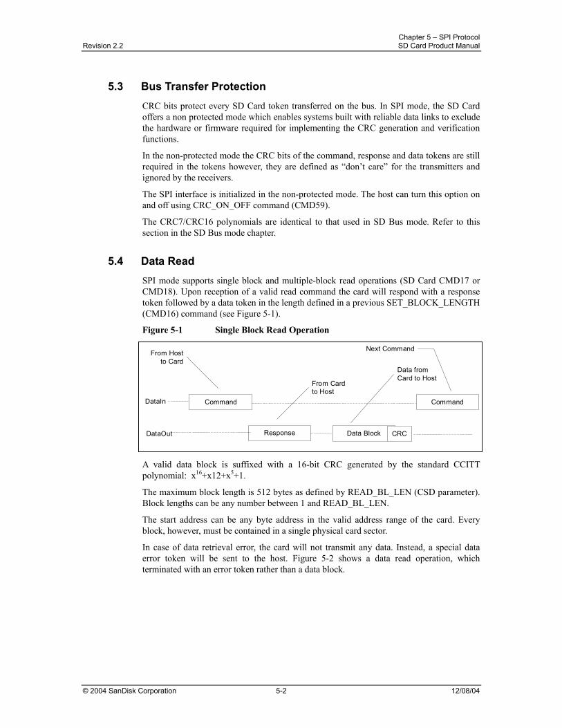
Chapter 5 – SPI Protocol Revision 2.2 SD Card Product Manual
© 2004 SanDisk Corporation 5-2 12/08/04
5.3 Bus Transfer Protection CRC bits protect every SD Card token transferred on the bus. In SPI mode, the SD Card offers a non protected mode which enables systems built with reliable data links to exclude the hardware or firmware required for implementing the CRC generation and verification functions.
In the non-protected mode the CRC bits of the command, response and data tokens are still required in the tokens however, they are defined as “don’t care” for the transmitters and ignored by the receivers.
The SPI interface is initialized in the non-protected mode. The host can turn this option on and off using CRC_ON_OFF command (CMD59).
The CRC7/CRC16 polynomials are identical to that used in SD Bus mode. Refer to this section in the SD Bus mode chapter.
5.4 Data Read SPI mode supports single block and multiple-block read operations (SD Card CMD17 or CMD18). Upon reception of a valid read command the card will respond with a response token followed by a data token in the length defined in a previous SET_BLOCK_LENGTH (CMD16) command (see Figure 5-1).
Figure 5-1 Single Block Read Operation
A valid data block is suffixed with a 16-bit CRC generated by the standard CCITT polynomial: x16+x12+x5+1.
The maximum block length is 512 bytes as defined by READ_BL_LEN (CSD parameter). Block lengths can be any number between 1 and READ_BL_LEN.
The start address can be any byte address in the valid address range of the card. Every block, however, must be contained in a single physical card sector.
In case of data retrieval error, the card will not transmit any data. Instead, a special data error token will be sent to the host. Figure 5-2 shows a data read operation, which terminated with an error token rather than a data block.
CommandDataIn Command
Response Data Block CRC
From Hostto Card
From Cardto Host
Data fromCard to Host
Next Command
DataOut
Chapter 5 – SPI Protocol Revision 2.2 SD Card Product Manual
© 2004 SanDisk Corporation 5-3 12/08/04
Figure 5-2 Read Operation—Data Error
In the case of a Multiple Block Read operation, every transferred block has a 16-bit CRC suffix. The Stop Transmission command (CMD12) will actually stop the data transfer operation (the same as in SD Bus mode).
Figure 5-3 Multiple Block Read Operation
5.5 Data Write In SPI mode, the SD Card supports single block or multiple-block write operations. Upon reception of a valid write command (SD Card CMD24 or CMD25), the card will respond with a response token and will wait for a data block to be sent from the host. CRC suffix and start address restrictions are identical to the read operation (see Figure 5-4). The only valid block length, however, is 512 bytes. Setting a smaller block length will cause a write error on the next write command.
Figure 5-4 Single Block Write Operation
CommandDataIn Command
Response Data Error
From Hostto Card
From Cardto Host
Data ErrorToken fromCard to Host
Next Command
DataOut
CommandDataIn
From hostto card(s)
DataOut
Command
From cardto host
From cardto host
Data Block CRCResponse Data Block CRC Response
StopTransmissioncommand
Data fromcard to host
CommandDataIn
From hostto card
Data fromhost tocard
DataOut
Data Block
Response Busy
Newcommandfrom host
From cardto host
Command
Response
Start blocktoken
Dataresponseand busyfrom card
Chapter 5 – SPI Protocol Revision 2.2 SD Card Product Manual
© 2004 SanDisk Corporation 5-4 12/08/04
Every data block has a prefix or ‘start block’ token (one byte). After a data block is received the card will respond with a data-response token, and if the data block is received with no errors, it will be programmed. As long as the card is busy programming, a continuous stream of busy tokens will be sent to the host (effectively holding the dataOut line low).
Once the programming operation is completed, the host must check the results of the programming using the SEND_STATUS command (CMD13). Some errors (e.g., address out of range, write protect violation, etc.) are detected during programming only. The only validation check performed on the data block and communicated to the host via the data-response token is CRC and general Write Error indication.
In multiple-block write operations, the stop transmission is done by sending, at the beginning of the next block, a Stop Tran token, instead of a Start Block token. In case of Write Error indication (on the data response) the host shall use SEND_NUM_WR_BLOCKS (ACMD22) in order to get the number of well written write blocks. The data token’s description is given in Section 5.17.
Figure 5-5 Multiple Block Write Operation
Resetting the CS signal while the card is busy does not terminate the programming process. The card releases the dataOut line (tristate) and continues to program. If the card is re-selected before the programming has finished, the dataOut line will be forced back to low and all commands will be rejected. Re-setting a card (using CMD0) will terminate any pending or active programming operation. This may destroy the data formats on the card. It is the host’s responsibility to prevent it.
5.6 Erase and Write Protect Management The erase and write protect management procedures in the SPI mode are identical to the SD Bus mode. While the card is erasing or changing the write protection bits of the predefined sector list it will be in a busy state and will hold the dataOut line low. Figure 5-6 illustrates a “no data” bus transaction with and without busy signaling.
CommandDataIn
From hostto card
Data fromhost tocard
DataOut
DataBlock
Data_Response Busy
Data fromhost tocard
From cardto host
Response
Start blocktoken
Dataresponseand busyfrom card
Data_Response Busy Busy
DataBlock
Stop trantoken
Chapter 5 – SPI Protocol Revision 2.2 SD Card Product Manual
© 2004 SanDisk Corporation 5-5 12/08/04
Figure 5-6 No Data Operations
5.7 Read CID/CSD Registers Unlike the SD bus protocol (where the register contents are sent as a command response), reading the contents of the CSD and CID registers in SPI mode is a simple read-block transaction. The card will respond with a standard response token followed by a data block of 16 bytes suffixed with a 16-bit CRC.
The data time out for the CSD command cannot be set to the card TAAC since this value is stored in the CSD. Therefore, the standard response time-out value (NCR) is used for read latency of the CSD Register.
5.8 Reset Sequence The SD Memory Card requires a defined reset sequence. After power on reset or CMD0 (software reset) the card enters an idle state. At this state the only valid host commands are ACMD41 (SD_SEND_OP_COND), CMD58 (READ_OCR) and CMD59 (CRC_ON_OFF). For the Thick (2.1mm) SD Memory Card - CMD1 (SEND_OP_COND) is also valid - that means that in SPI mode CMD1 and ACMD41 have the same behavior, though the usage of CMD41 is preferable because it allows easy distinguishing between SD Memory Card and MultiMediaCard. For the Thin (1.4mm) SD Card CMD1 (SEND_OP_COND) is illegal command during the initialization that is done after power on. After Power On, once the card accepted valid ACMD41, it will be able to accept also CMD1 even if used after re-initializing (CMD0) the card. It was defined in such way in order to be able to distinguish between Thin SD Memory Card and MultiMediaCards (that supports CMD1 as well).
The host must poll the card (by repeatedly sending CMD1 or ACMD41) until the ‘in-idle-state’ bit in the card response indicates (by being set to 0) that the card completed its initialization processes and is ready for the next command.
In SPI mode, as opposed to SD mode, ACMD41 (or CMD1 as well, for 2.1mm-SD Card) has no operands and does not return the contents of the OCR register. Instead, the host may use CMD58 (available in SPI mode only) to read the OCR register. Furthermore, it is in the responsibility of the host to refrain from accessing cards that do not support its voltage range.
The usage of CMD58 is not restricted to the initializing phase only, but can be issued at any time.
CommandDataIn
Response
From Hostto Card
From Hostto Card
DataOut
Command
Response Busy
From Cardto Host
From Cardto Host
Chapter 5 – SPI Protocol Revision 2.2 SD Card Product Manual
© 2004 SanDisk Corporation 5-6 12/08/04
5.9 Clock Control The SPI bus clock signal can be used by the SPI host to set the cards to energy-saving mode or to control the data flow (to avoid under-run or over-run conditions) on the bus. The host is allowed to change the clock frequency or shut it down. There are a few restrictions the SPI host must follow: • The bus frequency can be changed at any time (under the restrictions of maximum data
transfer frequency, defined by the SD cards). • It is an obvious requirement that the clock must be running for the SanDisk SD Card to
output data or response tokens. After the last SPI bus transaction, the host is required to provide 8 (eight) clock cycles for the card to complete the operation before shutting down the clock. Throughout this 8-clock period, the state of the CS signal is irrelevant. It can be asserted or de-asserted. Following is a list of the various SPI bus transactions: • A command/response sequence. Eight clocks after the card response end bit. The
CS signal can be asserted or de-asserted during these eight clocks. • A read data transaction; eight clocks after the end bit of the last data block. • A write data transaction; eight clocks after the CRC status token.
The host is allowed to shut down the clock of a “busy” card. The SD Card will complete the programming operation regardless of the host clock. However, the host must provide a clock edge for the card to turn off its busy signal. Without a clock edge, the SD Card (unless previously disconnected by de-asserting the CS signal) will force the dataOut line down, permanently.
5.10 Error Conditions The following sections provide valuable information on error conditions.
5.10.1 CRC and Illegal Commands Unlike the SD Card protocol, in SPI mode the card will always respond to a command. The response indicates acceptance or rejection of the command. A command may be rejected in any one of the following cases: • It is sent while the card is in read operation (except CMD12 which is legal). • It is sent while the card is in Busy. • Card is locked and it is other than Class 0 or 7 commands. • It is not supported (illegal opcode). • CRC check failed. • It contains an illegal operand. • It was out of sequence during an erase sequence. If the host sends a command while the card sends data in read operation then the response with an illegal command indication may disturb the data transfer.
5.10.2 Read, Write and Erase Time-out Conditions The times after which a time-out condition for read operations occur are (card independent) either 100 times longer than the typical access times for these operations given below or 100ms. The times after which a time-out condition for Write/Erase operations occur are (card independent) either 100 times longer than the typical program times for these operations given below or 250ms. A card shall complete the command within this time period, or give up and return an error message. If the host does not get any response with the given time out it should assume the card is not going to respond anymore and try to
Chapter 5 – SPI Protocol Revision 2.2 SD Card Product Manual
© 2004 SanDisk Corporation 5-7 12/08/04
recover (e.g., reset the card, power cycle, reject). The typical access and program times are defined in the following sections. Read The read access time is defined as the sum of the two times given by the CSD parameters TAAC and NSAC. These card parameters define the typical delay between the end bit of the read command and the start bit of the data block. Write The R2W_FACTOR field in the CSD is used to calculate the typical block program time obtained by multiplying the read access time by this factor. It applies to all write/erase commands (e.g., SET (CLEAR)_WRITE_PROTECT, PROGRAM_CSD (CID) and the block write commands). Erase The duration of an erase command will be (order of magnitude) the number of write blocks (WRITE_BL) to be erased multiplied by the block write delay.
5.11 Memory Array Partitioning See SD Card Bus Mode.
5.12 Card Lock/Unlock Usage of card lock and unlock commands in SPI mode is identical to SD mode. In both cases the command is responded with a R1b response type. After the busy signal clears, the host should obtain the result of the operation by issuing a GET_STATUS command.
5.13 Application-specific Commands The application-specific commands are identical to SD mode with the exception of the APP_CMD status bit, which is not available in SPI mode.
5.14 Copyright Protection Commands All the special copyright protection ACMDs and security functionality are the same as for SD Bus mode.
5.15 Switch Function Command Same as for SD mode with two exceptions: • The command is valid under the "not idle state". • In SPI mode, CMD0 switching period is within 8 clocks after the end bit of the CMD0
command R1 response.
5.16 High-speed Mode (25MB/sec interface speed) Not available in SPI Mode.
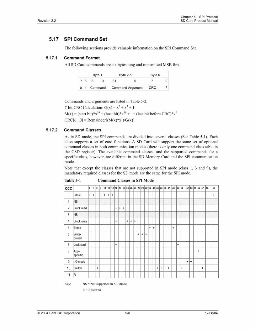
Chapter 5 – SPI Protocol Revision 2.2 SD Card Product Manual
© 2004 SanDisk Corporation 5-8 12/08/04
5.17 SPI Command Set The following sections provide valuable information on the SPI Command Set.
5.17.1 Command Format All SD Card commands are six bytes long and transmitted MSB first.
Commands and arguments are listed in Table 5-2. 7-bit CRC Calculation: G(x) = x7 + x3 + 1 M(x) = (start bit)*x39 + (host bit)*x38 +...+ (last bit before CRC)*x0 CRC[6...0] = Remainder[(M(x)*x7)/G(x)]
5.17.2 Command Classes As in SD mode, the SPI commands are divided into several classes (See Table 5-1). Each class supports a set of card functions. A SD Card will support the same set of optional command classes in both communication modes (there is only one command class table in the CSD register). The available command classes, and the supported commands for a specific class, however, are different in the SD Memory Card and the SPI communication mode. Note that except the classes that are not supported in SPI mode (class 1, 3 and 9), the mandatory required classes for the SD mode are the same for the SPI mode.
Table 5-1 Command Classes in SPI Mode
CCC 0 1 6 9 10 12 13 16 17 18 24 25 27 28 29 30 32 33 34 35 36 37 38 42 50 52 53 55 56 57 58 59
0 Basic + + + + + + + +
1 NS
2 Block read + + +
3 NS
4 Block write + + + +
5 Erase + + +
6 Write- protect
+ + +
7 Lock card + +
8 App-specific
+ +
9 I/O mode + +
10 Switch + + + + + + +
11 R Key: NS = Not supported in SPI mode.
R = Reserved
Byte 1 Byte 2-5 Byte 6
7 6 5 0 31 70 0
1CRCCommand ArgumentCommand0 1
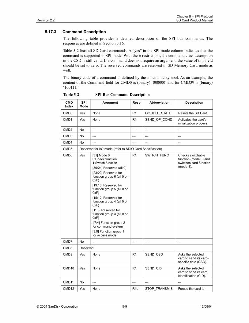
Chapter 5 – SPI Protocol Revision 2.2 SD Card Product Manual
© 2004 SanDisk Corporation 5-9 12/08/04
5.17.3 Command Description The following table provides a detailed description of the SPI bus commands. The responses are defined in Section 5.16.
Table 5-2 lists all SD Card commands. A “yes” in the SPI mode column indicates that the command is supported in SPI mode. With these restrictions, the command class description in the CSD is still valid. If a command does not require an argument, the value of this field should be set to zero. The reserved commands are reserved in SD Memory Card mode as well.
The binary code of a command is defined by the mnemonic symbol. As an example, the content of the Command field for CMD0 is (binary) ‘000000’ and for CMD39 is (binary) ‘100111.’
Table 5-2 SPI Bus Command Description
CMD Index
SPI Mode
Argument Resp Abbreviation Description
CMD0 Yes None R1 GO_IDLE_STATE Resets the SD Card.
CMD1 Yes None R1 SEND_OP_COND Activates the card’s initialization process.
CMD2 No --- --- --- ---
CMD3 No --- --- --- ---
CMD4 No --- --- --- ---
CMD5 Reserved for I/O mode (refer to SDIO Card Specification).
CMD6 Yes [31] Mode 0 0:Check function 1:Switch function [30:24] Reserved (all 0) [23:20] Reserved for function group 6 (all 0 or 0xF) [19:16] Reserved for function group 5 (all 0 or 0xF) [15:12] Reserved for function group 4 (all 0 or 0xF) [11:8] Reserved for function group 3 (all 0 or 0xF) [7:4] Function group 2 for command system [3:0] Function group 1 for access mode.
R1 SWITCH_FUNC Checks switchable function (mode 0) and switches card function (mode 1).
CMD7 No --- --- --- ---
CMD8 Reserved.
CMD9 Yes None R1 SEND_CSD Asks the selected card to send its card-specific data (CSD).
CMD10 Yes None R1 SEND_CID Asks the selected card to send its card identification (CID).
CMD11 No --- --- --- ---
CMD12 Yes None R1b STOP_TRANSMISSION
Forces the card to t t i i
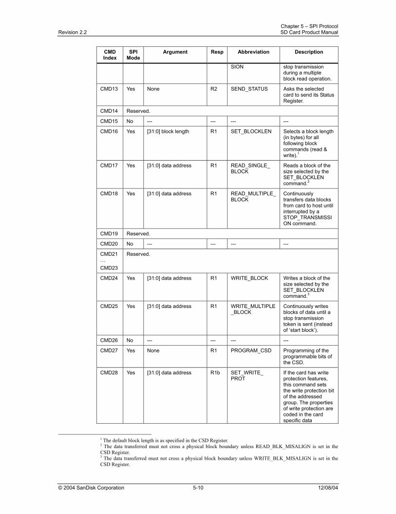
Chapter 5 – SPI Protocol Revision 2.2 SD Card Product Manual
© 2004 SanDisk Corporation 5-10 12/08/04
CMD Index
SPI Mode
Argument Resp Abbreviation Description
SION stop transmission during a multiple block read operation.
CMD13 Yes None R2 SEND_STATUS Asks the selected card to send its Status Register.
CMD14 Reserved.
CMD15 No --- --- --- ---
CMD16 Yes [31:0] block length R1 SET_BLOCKLEN Selects a block length (in bytes) for all following block commands (read & write).1
CMD17 Yes [31:0] data address R1 READ_SINGLE_ BLOCK
Reads a block of the size selected by the SET_BLOCKLEN command.2
CMD18 Yes [31:0] data address R1 READ_MULTIPLE_BLOCK
Continuously transfers data blocks from card to host until interrupted by a STOP_TRANSMISSION command.
CMD19 Reserved.
CMD20 No --- --- --- ---
CMD21 … CMD23
Reserved.
CMD24 Yes [31:0] data address R1 WRITE_BLOCK Writes a block of the size selected by the SET_BLOCKLEN command.3
CMD25 Yes [31:0] data address R1 WRITE_MULTIPLE_BLOCK
Continuously writes blocks of data until a stop transmission token is sent (instead of ‘start block’).
CMD26 No --- --- --- ---
CMD27 Yes None R1 PROGRAM_CSD Programming of the programmable bits of the CSD.
CMD28 Yes [31:0] data address R1b SET_WRITE_ PROT
If the card has write protection features, this command sets the write protection bit of the addressed group. The properties of write protection are coded in the card specific data
1 The default block length is as specified in the CSD Register. 2 The data transferred must not cross a physical block boundary unless READ_BLK_MISALIGN is set in the CSD Register. 3 The data transferred must not cross a physical block boundary unless WRITE_BLK_MISALIGN is set in the CSD Register.
Chapter 5 – SPI Protocol Revision 2.2 SD Card Product Manual
© 2004 SanDisk Corporation 5-11 12/08/04
CMD Index
SPI Mode
Argument Resp Abbreviation Description
(WP_GRP_SIZE).
CMD29 Yes [31:0] data address R1b CLR_WRITE_ PROT
If the card has write protection features, this command clears the write protection bit of the addressed group.
CMD30 Yes [31:0] write protect data address
R1 SEND_WRITE_ PROT
If the card has write protection features, this command asks the card to send the status of the write protection bits.
CMD31 Reserved
CMD32 Yes [31:0] data address R1 ERASE_WR_BLK_ START_ADDR
Sets the address of the first write block to be erased.
CMD33 Yes [31:0] data address R1 ERASE_WR_BLK_ END_ADDR
Sets the address of the last write block in a continuous range to be erased.
CMD34 … CMD37
Reserved for each command system set by switch function command (CMD6). Detailed definition can be referenced in each command system specification.
CMD38 Yes [31:0] stuff bits R1b ERASE Erases all previously selected write blocks.
CMD39 No --- --- --- ---
CMD40 No --- --- --- ---
CMD41 Reserved
CMD42 Yes [31:0] stuff bits R1 LOCK_UNLOCK Used to set/re-set the password or lock/unlock the card. A transferred data block includes all the command details. The size of the data block is defined with SET_BLOCK_LEN command.
CMD43-CMD49 CMD51
Reserved.
CMD50 Reserved for each command system set by switch function command (CMD6). Detailed definition can be referenced in each command system specification.
CMD52… CMD54
Reserved for I/O mode (refer to SDIO Card Specification).
CMD55 Yes [31:0] stuff bits R1 APP_CMD Notifies the card that the next command is an application-specific command rather than a standard command.
Chapter 5 – SPI Protocol Revision 2.2 SD Card Product Manual
© 2004 SanDisk Corporation 5-12 12/08/04
CMD Index
SPI Mode
Argument Resp Abbreviation Description
CMD56 Yes [31:0] stuff bits, [0]: RD/WR4
R1 GEN_CMD Used either to transfer a Data Block to the card or to get a Data Block from the card for general purpose/application specific commands. The size of the Data Block is defined with SET_BLOCK_LEN command.
CMD57 Reserved for each command system set by switch function command (CMD6). Detailed definition can be referenced in each command system specification.
CMD58 Yes None R3 READ_OCR Reads the OCR Register of a card.
CMD59 Yes [31:1] stuff bits, [0:0] CRC option
R1 CRC_ON_OFF Turns the CRC option on or off. A ‘1’ in the CRC option bit will turn the option on, a ‘0’ will turn it off.
CMD60-CMD63
Reserved for manufacturer.
5.18 Responses There are several types of response tokens. As in the SD mode, all are transmitted MSB first.
5.18.1 Format R1 The card sends this response token after every command with the exception of SEND_STATUS commands. It is 1-byte long, the MSB is always set to zero and the other bits are error indications; ‘1’ signals error. • Idle state—The card is in idle state and running initializing process. • Erase reset—An erase sequence was cleared before executing because an out of erase
sequence command was received. • Illegal command—An illegal command code was detected. • Communication CRC error—The CRC check of the last command failed. • Erase sequence error—An error in the sequence of erase commands occurred. • Address error—A misaligned address, which did not match the block length was used
in the command. • Parameter error—The command’s argument (e.g., address, block length) was out of the
allowed range for this card.
4 RD/WR: 1 = host will get a block of data from the card. 0 = host sends block of data to the card.
Chapter 5 – SPI Protocol Revision 2.2 SD Card Product Manual
© 2004 SanDisk Corporation 5-13 12/08/04
The structure of the R1 format is shown in Figure 5-7.
Figure 5-7 R1 Response Format
5.18.2 Format R1b This response token is identical to R1 format with the optional addition of the busy signal. The busy signal token can be any number of bytes. A zero value indicates card is busy. A non-zero value indicates card is ready for the next command.
5.18.3 Format R2 This response token is two bytes long and sent as a response to the SEND_STATUS command. The format of the R2 status is shown in Figure 5-8.
Figure 5-8 R2 Response Format
First byte is identical to response R1. The content of the second byte is described below.
• Erase param—An invalid selection, sectors for erase. • Write-protect (WP) violation—The command tried to write a write-protected block. • Card ECC failed—Card internal ECC was applied but failed to correct the data. • CC error—Internal card-controller error. • Error—A general or an unknown error occurred during the operation. • Write-protect erase-skip/lock/unlock command failed—This status bit has two
functions overloaded. It is set when the host attempts to erase a write-protected sector or makes a sequence or password error during card lock/unlock operation.
• Card is locked—Set when the user locks the card. Resets when it is unlocked.
7
0
0
Idle StateErase ResetIllegal CommandCom CRC ErrorErase Seq ErrorAddress ErrorParameter Error
7
0
0 7 0Byte 1 Byte 2
Com CRC Error
Address Error
Idle State
CC Error
WP Violation
Card is LockedWP EraseSkip, Lock/Unlock Cmd FailedError
Erase Parameter
Parameter Error
Erase ResetIllegal Command
Erase Sequence Error
Card ECC Failed
Out-of-Range, CSD_Overwrite
Chapter 5 – SPI Protocol Revision 2.2 SD Card Product Manual
© 2004 SanDisk Corporation 5-14 12/08/04
5.18.4 Format R3 The SD Card sends this response token when an READ_OCR command is received. The response length is five bytes. The structure of the first (MSB) byte is identical to response type R1. The other four bytes contain the OCR Register.
Figure 5-9 R3 Response Format
5.18.5 Formats R4 and R5 These response formats are reserved for I/O mode (refer to SDIO Card Specification).
5.18.6 Data Response Every data block written to the card is acknowledged by a data response token. It is one-byte long and has the following format:
The meaning of the status bits is defined as follows: ‘010’—Data accepted. ‘101’—Data rejected due to a CRC error. ‘110’—Data rejected due to a Write Error In case of any error (CRC or Write) during Write Multiple Block operation, the host will stop the data transmission using CMD12. In case of Write Error (response ’110’) the host may send CMD13 (SEND_STATUS) in order to get the cause of the write problem. ACMD22 can be used to find the number of well-written write blocks.
5.19 Data Tokens Read and write commands have data transfers associated with them; data is transmitted or received via data tokens. All data bytes are transmitted MSB. Data tokens are 4 to 515 bytes long and have the following format: Single-Block Read, Single-Block Write and Multiple-Block Read: • First byte: Start Block. • Bytes 2-513 (depends on the data block length): User Data. • Last two bytes: 16-bit CRC.
39
0
32 31 0
R1 OCR
7
x x x 0
0
Status 1
6
7
1
0
01 1 1 1 1 1
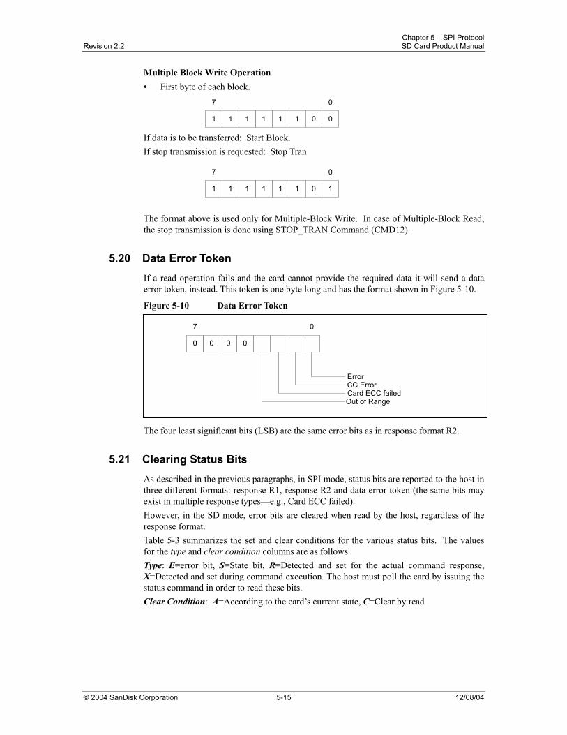
Chapter 5 – SPI Protocol Revision 2.2 SD Card Product Manual
© 2004 SanDisk Corporation 5-15 12/08/04
Multiple Block Write Operation • First byte of each block.
If data is to be transferred: Start Block. If stop transmission is requested: Stop Tran
The format above is used only for Multiple-Block Write. In case of Multiple-Block Read, the stop transmission is done using STOP_TRAN Command (CMD12).
5.20 Data Error Token If a read operation fails and the card cannot provide the required data it will send a data error token, instead. This token is one byte long and has the format shown in Figure 5-10.
Figure 5-10 Data Error Token
The four least significant bits (LSB) are the same error bits as in response format R2.
5.21 Clearing Status Bits As described in the previous paragraphs, in SPI mode, status bits are reported to the host in three different formats: response R1, response R2 and data error token (the same bits may exist in multiple response types—e.g., Card ECC failed). However, in the SD mode, error bits are cleared when read by the host, regardless of the response format. Table 5-3 summarizes the set and clear conditions for the various status bits. The values for the type and clear condition columns are as follows. Type: E=error bit, S=State bit, R=Detected and set for the actual command response, X=Detected and set during command execution. The host must poll the card by issuing the status command in order to read these bits. Clear Condition: A=According to the card’s current state, C=Clear by read
7
1
0
01 1 1 1 1 0
7
1
0
11 1 1 1 1 0
7
0 0 0 0
0
ErrorCC ErrorCard ECC failedOut of Range
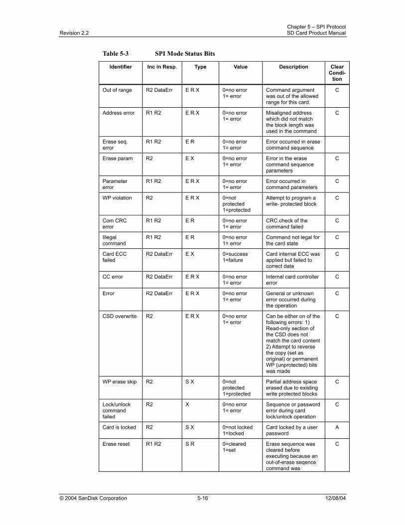
Chapter 5 – SPI Protocol Revision 2.2 SD Card Product Manual
© 2004 SanDisk Corporation 5-16 12/08/04
Table 5-3 SPI Mode Status Bits
Identifier Inc in Resp. Type Value Description Clear Condi-
tion
Out of range R2 DataErr E R X 0=no error 1= error
Command argument was out of the allowed range for this card.
C
Address error R1 R2 E R X 0=no error 1= error
Misaligned address which did not match the block length was used in the command
C
Erase seq. error
R1 R2 E R 0=no error 1= error
Error occurred in erase command sequence
Erase param R2 E X 0=no error 1= error
Error in the erase command sequence parameters
C
Parameter error
R1 R2 E R X 0=no error 1= error
Error occurred in command parameters
C
WP violation R2 E R X 0=not protected 1=protected
Attempt to program a write- protected block
C
Com CRC error
R1 R2 E R 0=no error 1= error
CRC check of the command failed
C
Illegal command
R1 R2 E R 0=no error 1= error
Command not legal for the card state
C
Card ECC failed
R2 DataErr E X 0=success 1=failure
Card internal ECC was applied but failed to correct data
C
CC error R2 DataErr E R X 0=no error 1= error
Internal card controller error
C
Error R2 DataErr E R X 0=no error 1= error
General or unknown error occurred during the operation
C
CSD overwrite R2 E R X 0=no error 1= error
Can be either on of the following errors: 1) Read-only section of the CSD does not match the card content 2) Attempt to reverse the copy (set as original) or permanent WP (unprotected) bits was made
C
WP erase skip R2 S X 0=not protected 1=protected
Partial address space erased due to existing write protected blocks
C
Lock/unlock command failed
R2 X 0=no error 1= error
Sequence or password error during card lock/unlock operation
C
Card is locked R2 S X 0=not locked 1=locked
Card locked by a user password
A
Erase reset R1 R2 S R 0=cleared 1=set
Erase sequence was cleared before executing because an out-of-erase seqence command was
C
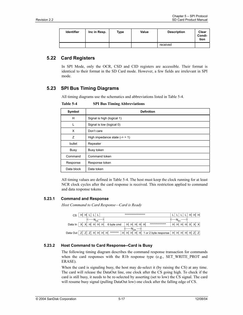
Chapter 5 – SPI Protocol Revision 2.2 SD Card Product Manual
© 2004 SanDisk Corporation 5-17 12/08/04
Identifier Inc in Resp. Type Value Description Clear Condi-
tion received
5.22 Card Registers In SPI Mode, only the OCR, CSD and CID registers are accessible. Their format is identical to their format in the SD Card mode. However, a few fields are irrelevant in SPI mode.
5.23 SPI Bus Timing Diagrams All timing diagrams use the schematics and abbreviations listed in Table 5-4.
Table 5-4 SPI Bus Timing Abbreviations
Symbol Definition
H Signal is high (logical 1)
L Signal is low (logical 0)
X Don’t care
Z High impedance state (-> = 1)
bullet Repeater
Busy Busy token
Command Command token
Response Response token
Data block Data token
All timing values are defined in Table 5-4. The host must keep the clock running for at least NCR clock cycles after the card response is received. This restriction applied to command and data response tokens.
5.23.1 Command and Response Host Command to Card Response—Card is Ready
5.23.2 Host Command to Card Response--Card is Busy The following timing diagram describes the command response transaction for commands when the card responses with the R1b response type (e.g., SET_WRITE_PROT and ERASE). When the card is signaling busy, the host may de-select it (by raising the CS) at any time. The card will release the DataOut line, one clock after the CS going high. To check if the card is still busy, it needs to be re-selected by asserting (set to low) the CS signal. The card will resume busy signal (pulling DataOut low) one clock after the falling edge of CS.
X X H H H H
Z Z Z H H H H
H H L L L *******************
6 byte cmd H H H H H ***************
H H H H H********
H H H H X X X
1 or 2 byte response H H H H H Z Z
L L L L H H H
NCS NEC
NCR
CS
Data In
Data Out
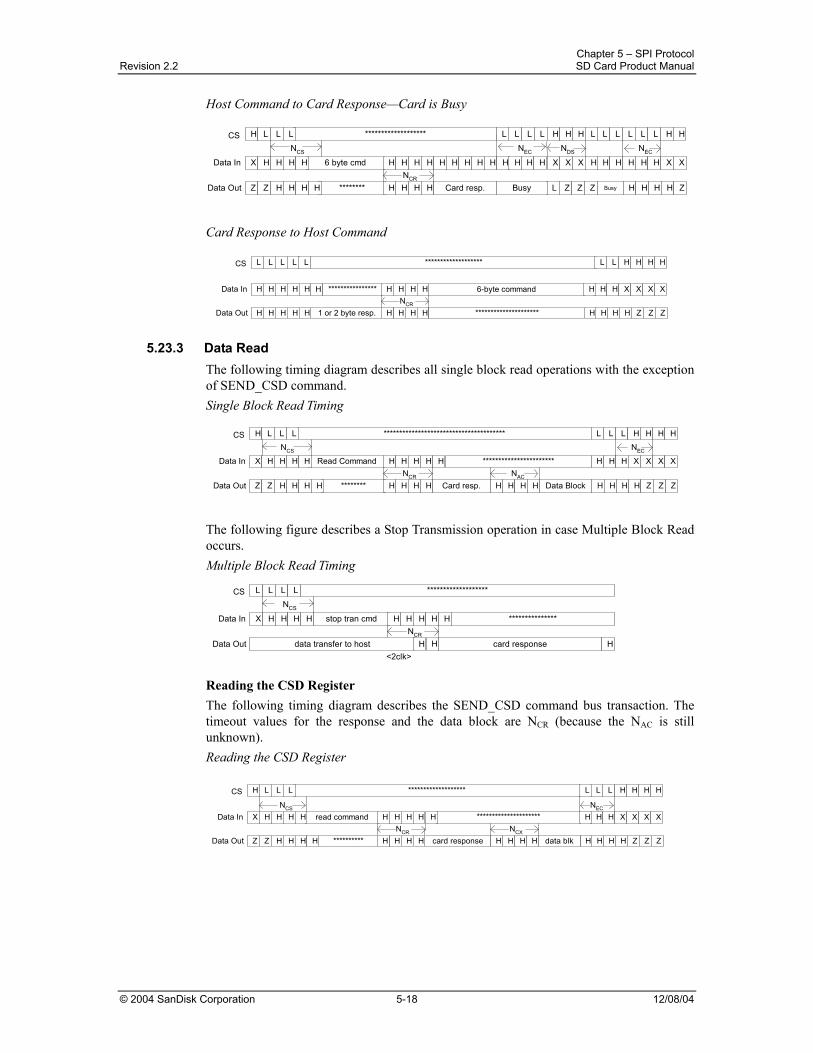
Chapter 5 – SPI Protocol Revision 2.2 SD Card Product Manual
© 2004 SanDisk Corporation 5-18 12/08/04
Host Command to Card Response—Card is Busy
Card Response to Host Command
5.23.3 Data Read The following timing diagram describes all single block read operations with the exception of SEND_CSD command. Single Block Read Timing
The following figure describes a Stop Transmission operation in case Multiple Block Read occurs. Multiple Block Read Timing
Reading the CSD Register The following timing diagram describes the SEND_CSD command bus transaction. The timeout values for the response and the data block are NCR (because the NAC is still unknown). Reading the CSD Register
X H H H
Z Z H H H
H L L *******************
6 byte cmd H H H H H
H H H********
H H X X X H H
Card resp. L Z Z Z
H
L L L L L H H
NCS NEC
NCR
CS
Data In
Data Out
L L L H H H LL
H H H H H H H
H H Busy Busy
H H H X X
H H H H Z
L
NDS NEC
H H H H
H H H H
L L L *******************
****************
H H H1 or 2 byte resp. ********************* H H
H
L H H H H
NCR
CS
Data In
Data Out
L
H
H
H X X X X
H H Z Z Z
L
H 6-byte commandH H H H H
H
L
X H H H
Z Z H H H
H L L ***************************************
Read Command H H H H H
H H H********
H
Card resp. H H
H
L L L H H H H
NCS
NCR
CS
Data In
Data Out
L
H
H H
H X X X X
H H Z Z Z
NEC
***********************
Data BlockH H HHNAC
X H H H H
L L L *******************
stop tran cmd H H H H H ***************
data transfer to host card response H
NCS
NCR
CS
Data In
Data Out
L
HH<2clk>
X H H H
Z Z H H
H L L *******************
read command
********** card response H H
H
L H H H H
NCR
CS
Data In
Data Out
L
H H X X X X
H H Z Z Z
L
*********************H H H H H
H
L
H H H HH H H HH data blk
HNCS
NCX
NEC
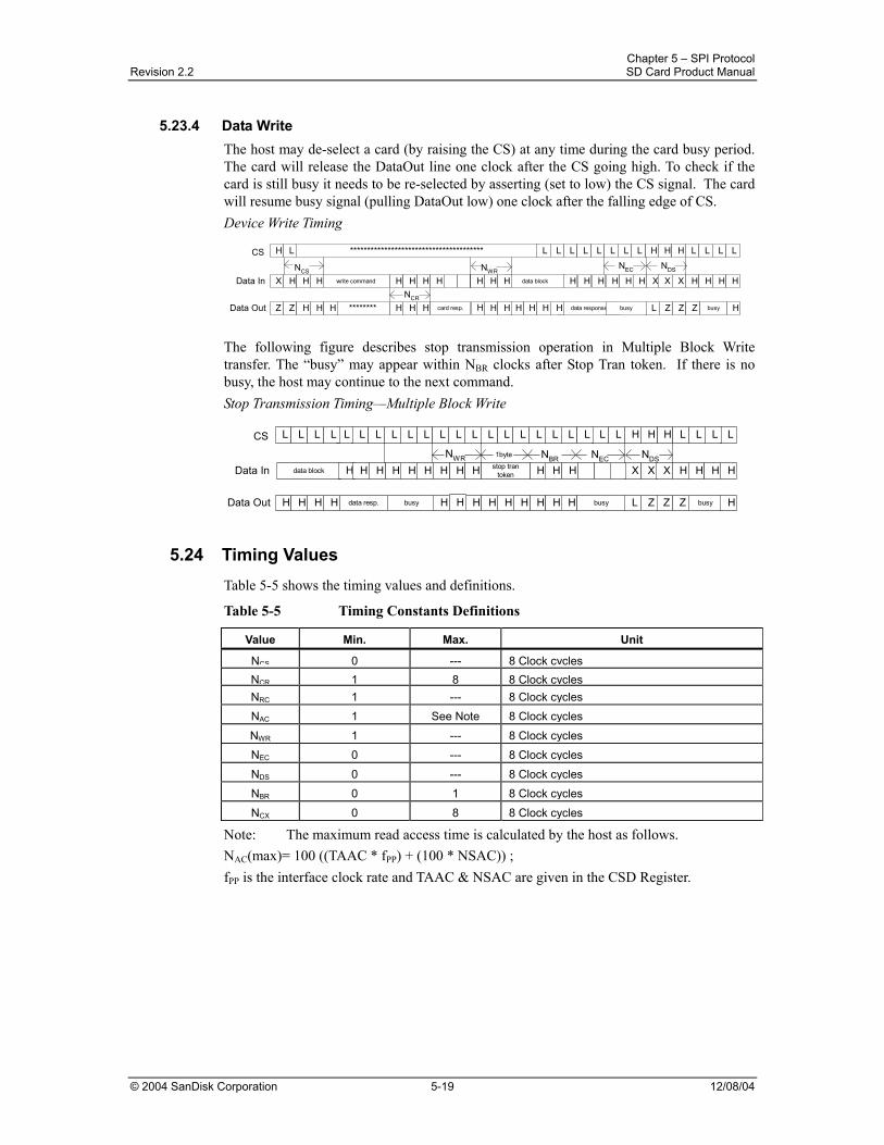
Chapter 5 – SPI Protocol Revision 2.2 SD Card Product Manual
© 2004 SanDisk Corporation 5-19 12/08/04
5.23.4 Data Write The host may de-select a card (by raising the CS) at any time during the card busy period. The card will release the DataOut line one clock after the CS going high. To check if the card is still busy it needs to be re-selected by asserting (set to low) the CS signal. The card will resume busy signal (pulling DataOut low) one clock after the falling edge of CS. Device Write Timing
The following figure describes stop transmission operation in Multiple Block Write transfer. The “busy” may appear within NBR clocks after Stop Tran token. If there is no busy, the host may continue to the next command. Stop Transmission Timing—Multiple Block Write
5.24 Timing Values Table 5-5 shows the timing values and definitions.
Table 5-5 Timing Constants Definitions
Value Min. Max. Unit
NCS 0 --- 8 Clock cyclesNCR 1 8 8 Clock cyclesNRC 1 --- 8 Clock cyclesNAC 1 See Note 8 Clock cycles
NWR 1 --- 8 Clock cyclesNEC 0 --- 8 Clock cycles
NDS 0 --- 8 Clock cyclesNBR 0 1 8 Clock cycles
NCX 0 8 8 Clock cycles
Note: The maximum read access time is calculated by the host as follows. NAC(max)= 100 ((TAAC * fPP) + (100 * NSAC)) ; fPP is the interface clock rate and TAAC & NSAC are given in the CSD Register.
X H H
Z Z H H
H ***************************************
write command H H H
H H********
X
card resp. L Z
X
H H H
NCS
NCR
CS
Data In
Data Out H
X H H H H
Z Z H
NEC
data block
data responseH H HH
L L L LL L L LL L L LL
H
H H H H HH H H H HH
H H H busybusy
HNWR
NDS
H H H H
L
H H H
Z
L
1byte
CS
Data In
Data Out
NECdata block
H
L
X X H H HH H HH
H H busybusy
XNWR NBR
H L L LL L H HL L L L L LL L L LL L L LL LL L
H HHH H H stop trantoken
ZL Zdata resp. busy H H H H H H H
NDS
Chapter 5 – SPI Protocol Revision 2.2 SD Card Product Manual
© 2004 SanDisk Corporation 5-20 12/08/04
5.25 SPI Electrical Interface The SPI Mode electrical interface is identical to that of the SD Card mode.
5.26 SPI Bus Operating Conditions See SD Card mode.
5.27 Bus Timing See SD Card mode. The timing of the CS signal is the same as any other card input.
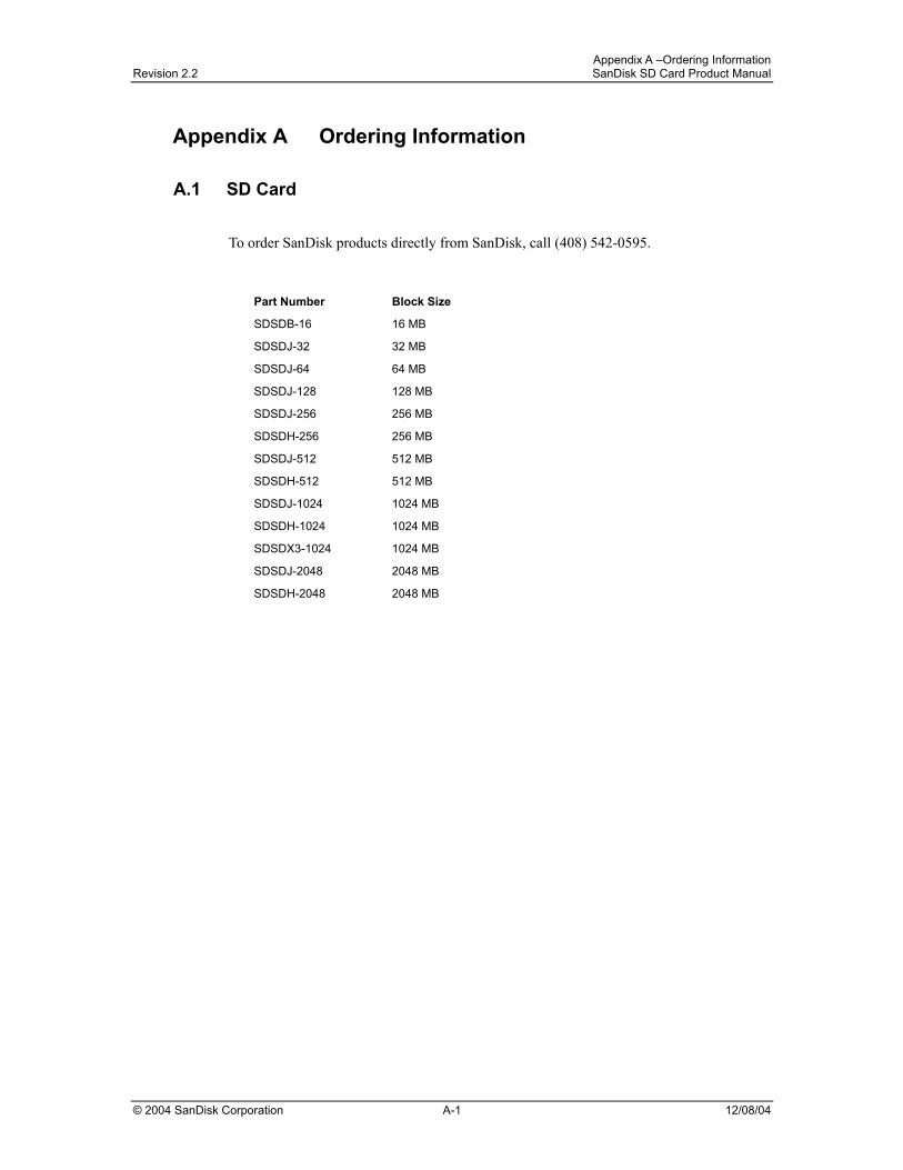
Appendix A –Ordering Information Revision 2.2 SanDisk SD Card Product Manual
© 2004 SanDisk Corporation A-1 12/08/04
Appendix A Ordering Information
A.1 SD Card To order SanDisk products directly from SanDisk, call (408) 542-0595.
Part Number Block Size
SDSDB-16 16 MB
SDSDJ-32 32 MB
SDSDJ-64 64 MB
SDSDJ-128 128 MB
SDSDJ-256 256 MB
SDSDH-256 256 MB
SDSDJ-512 512 MB
SDSDH-512 512 MB
SDSDJ-1024 1024 MB
SDSDH-1024 1024 MB
SDSDX3-1024 1024 MB
SDSDJ-2048 2048 MB
SDSDH-2048 2048 MB
Appendix B –SanDisk Worldwide Sales Offices Revision 2.2 SanDisk SD Card Product Manual
© 2004 SanDisk Corporation B-1 12/08/04
Appendix B SanDisk Worldwide Sales Offices
To order SanDisk products directly from SanDisk, call (408) 542-0595.
SanDisk Corporate Headquarters 140 Caspian Court Sunnyvale, CA 94089 Tel: 408-542-0500 Fax: 408-542-0503 http://www.sandisk.com U.S. Industrial/OEM Sales Offices
Southwest, Northwest USA & Mexico140 Caspian Court Sunnyvale, CA 94089 Tel: 408-542-0730 Fax: 408-542-0410
North Central USA & South America 134 Cherry Creek Circle, Suite 150 Winter Springs, FL 32708 Tel: 407-366-6490 Fax: 407-366-5945
Northeastern USA & Canada 620 Herndon Pkwy. Suite 200 Herndon, VA 22070 Tel: 703-481-9828 Fax: 703-437-9215
International Industrial/OEM Sales Offices
Europe SanDisk GmbH Karlsruher Str. 2C D-30519 Hannover, Germany Tel: 49-511-875-9131 Fax: 49-511-875-9187
Northern Europe Videroegatan 3 B S-16440 Kista, Sweden Tel: 46-08-75084-63 Fax: 46-08-75084-26
Central & Southern Europe Rudolf-Diesel-Str. 3 40822 Mettmann, Germany Tel: 49-210-495-3433 Fax: 49-210-495-3434
Japan 8F Nisso Bldg. 15 2-17-19 Shin-Yokohama, Kohoku-ku Yokohama 222-0033, Japan Tel: 81-45-474-0181 Fax: 81-45-474-0371
Asia/Pacific Rim Suite 902-903 Bank of East Asia Harbour View Centre 56 Gloucester Road, Wanchai Hong Kong Tel: 852-2712-0501 Fax: 852-2712-9385
Appendix C –Limited Warranty Revision 2.2 SanDisk SD Card Product Manual
© 2004 SanDisk Corporation C-1 12/08/04
Appendix C Limited Warranty I. WARRANTY STATEMENT
SanDisk warrants its products to be free of any defects in materials or workmanship that would prevent them from functioning properly for one year from the date of purchase. This express warranty is extended by SanDisk Corporation. II. GENERAL PROVISIONS
This warranty sets forth the full extent of SanDisk’s responsibilities regarding the SanDisk SD Card. In satisfaction of its obligations hereunder, SanDisk, at its sole option, will repair, replace or refund the purchase price of the product. NOTWITHSTANDING ANYTHING ELSE IN THIS LIMITED WARRANTY OR OTHERWISE, THE EXPRESS WARRANTIES AND OBLIGATIONS OF SELLER AS SET FORTH IN THIS LIMITED WARRANTY, ARE IN LIEU OF, AND BUYER EXPRESSLY WAIVES ALL OTHER OBLIGATIONS, GUARANTIES AND WARRANTIES OF ANY KIND, WHETHER EXPRESS OR IMPLIED, INCLUDING WITHOUT LIMITATION, ANY IMPLIED WARRANTY OF MERCHANTABILITY OR FITNESS FOR A PARTICULAR PURPOSE OR INFRINGEMENT, TOGETHER WITH ANY LIABILITY OF SELLER UNDER ANY CONTRACT, NEGLIGENCE, STRICT LIABILITY OR OTHER LEGAL OR EQUITABLE THEORY FOR LOSS OF USE, REVENUE, OR PROFIT OR OTHER INCIDENTAL OR CONSEQUENTIAL DAMAGES, INCLUDING WITHOUT LIMITATION PHYSICAL INJURY OR DEATH, PROPERTY DAMAGE, LOST DATA, OR COSTS OF PROCUREMENT OF SUBSTITUTE GOODS, TECHNOLOGY OR SERVICES. IN NO EVENT SHALL THE SELLER BE LIABLE FOR DAMAGES IN EXCESS OF THE PURCHASE PRICE OF THE PRODUCT, ARISING OUT OF THE USE OR INABILITY TO USE SUCH PRODUCT, TO THE FULL EXTENT SUCH MAY BE DISCLAIMED BY LAW.
SanDisk’s products are not warranted to operate without failure. Accordingly, in any use of products in life support systems or other applications where failure could cause injury or loss of life, the products should only be incorporated in systems designed with appropriate redundancy, fault tolerant or back-up features. III. WHAT THIS WARRANTY COVERS
For products found to be defective within one year of purchase, SanDisk will have the option of repairing or replacing the defective product, if the following conditions are met:
A. A warranty registration card for each defective product was submitted and is on file at SanDisk. If not, a warranty registration card must accompany each returned defective product. This card is included in each product’s original retail package.
B. The defective product is returned to SanDisk for failure analysis as soon as possible after the failure occurs.
C. An incident card filled out by the user, explaining the conditions of usage and the nature of the failure, accompanies each returned defective product.
D. No evidence is found of abuse or operation of products not in accordance with the published specifications, or of exceeding storage or maximum ratings or operating conditions.
All failing products returned to SanDisk under the provisions of this limited warranty shall be tested to the product’s functional and performance specifications. Upon confirmation of failure, each product will be analyzed, by whatever means necessary, to determine the root cause of failure. If the
Appendix C –Limited Warranty Revision 2.2 SanDisk SD Card Product Manual
© 2004 SanDisk Corporation C-2 12/08/04
root cause of failure is found to be not covered by the above provisions, then the product will be returned to the customer with a report indicating why the failure was not covered under the warranty.
This warranty does not cover defects, malfunctions, performance failures or damages to the unit resulting from use in other than its normal and customary manner, misuse, accident or neglect; or improper alterations or repairs.
SanDisk reserves the right to repair or replace, at its discretion, any product returned by its customers, even if such product is not covered under warranty, but is under no obligation to do so.
SanDisk may, at its discretion, ship repaired or rebuilt products identified in the same way as new products, provided such cards meet or exceed the same published specifications as new products. Concurrently, SanDisk also reserves the right to market any products, whether new, repaired, or rebuilt, under different specifications and product designations if such products do not meet the original product’s specifications.
IV. RECEIVING WARRANTY SERVICE According to SanDisk’s warranty procedure, defective product should be returned only with prior authorization from SanDisk Corporation. Please contact SanDisk’s Customer Service department at 408-542-0595 with the following information: product model number and description, serial numbers, nature of defect, conditions of use, proof of purchase and purchase date. If approved, SanDisk will issue a Return Material Authorization or Product Repair Authorization number. Ship the defective product to:
SanDisk Corporation Attn: RMA Returns (Reference RMA or PRA #) 140 Caspian Court Sunnyvale, CA 94089
V. STATE LAW RIGHTS
SOME STATES DO NOT ALLOW THE EXCLUSION OR LIMITATION OF INCIDENTAL OR CONSEQUENTIAL DAMAGES, OR LIMITATION ON HOW LONG AN IMPLIED WARRANTY LASTS, SO THE ABOVE LIMITATIONS OR EXCLUSIONS MAY NOT APPLY TO YOU. This warranty gives you specific rights and you may also have other rights that vary from state to state.
Appendix D –Disclaimer of Liability Revision 2.2 SanDisk SD Card Product Manual
© 2004 SanDisk Corporation D-1 12/08/04
Appendix D Disclaimer of Liability
D.1 SanDisk Corporation Policy SanDisk Corporation general policy does not recommend the use of its products in life support applications wherein a failure or malfunction of the product may directly threaten life or injury. Accordingly, in any use of products in life support systems or other applications where failure could cause damage, injury or loss of life, the products should only be incorporated in systems designed with appropriate redundancy, fault tolerant or back-up features. SanDisk shall not be liable for any loss, injury or damage caused by use of the Products in any of the following applications:
− Special applications such as military related equipment, nuclear reactor control, and aerospace
− Control devices for automotive vehicles, train, ship and traffic equipment
− Safety system for disaster prevention and crime prevention
− Medical-related equipment including medical measurement device
Appendix D –Disclaimer of Liability Revision 2.2 SanDisk SD Card Product Manual
© 2004 SanDisk Corporation E-1 12/08/04
Appendix E Application Note
E.1 Host Design Considerations: NAND MMC and SD-based Products SanDisk Application Note for the SanDisk SD Card follows.
Host Design Considerations: NAND MMC and SD-based Products
Application Note Version 1.0
Document No. 80-11-00160 September 30, 2002
SanDisk Corporation Corporate Headquarters • 140 Caspian Court • Sunnyvale, CA 94089
Phone (408) 542-0500 • Fax (408) 542-0503 www.sandisk.com
Host Design Considerations: Application Note NAND MMC and SD-based Products Revision 1.0
© 2002 SanDisk Corporation 2 9/30/02, Lit# 80-11-00160
SanDisk® Corporation general policy does not recommend the use of its products in life support applications where in a failure or malfunction of the product may directly threaten life or injury. Per SanDisk Terms and Conditions of Sale, the user of SanDisk products in life support applications assumes all risk of such use and indemnifies SanDisk against all damages. The information in this document is subject to change without notice. SanDisk Corporation shall not be liable for technical or editorial errors or omissions contained herein; nor for incidental or consequential damages resulting from the furnishing, performance, or use of this material. All portions of SanDisk documentation are protected by copyright law and all rights are reserved. This documentation may not, in whole or in part, be copied, photocopied, reproduced, translated, or reduced to any electronic medium or machine-readable form without prior consent, in writing, from SanDisk Corporation. SanDisk and the SanDisk logo are registered trademarks of SanDisk Corporation. Product names mentioned herein are for identification purposes only and may be trademarks and/or registered trademarks of their respective companies. © 2002 SanDisk Corporation. All rights reserved. SanDisk products are covered or licensed under one or more of the following U.S. Patent Nos. 5,070,032; 5,095,344; 5,168,465; 5,172,338; 5,198,380; 5,200,959; 5,268,318; 5,268,870; 5,272,669; 5,418,752; 5,602,987. Other U.S. and foreign patents awarded and pending. Lit. No. 80-11-00160 Rev. 1.0, Created on 9/26/2002 1:34 PM Printed in U.S.A. Revision History • Revision 1.0—initial release.
Host Design Considerations: Application Note NAND MMC and SD-based Products Revision 1.0
© 2002 SanDisk Corporation 3 9/30/02, Lit# 80-11-00160
Introduction SanDisk’s MultiMediaCard (MMC) and Secure Digital (SD) Card have been designed into a wide variety of consumer electronic products: MP3 players, cell phones, PDAs, digital still and video cameras, data loggers, and more. Although these cards were designed to support this wide range of products, there are many options an engineer needs to consider before designing a card slot into a product. Design considerations include how the end product handles timeout delays, bus type selection, block mode selection, and other options. These can have a major impact on the performance and compatibility of the product. This Application Note will review these options and provide recommendations on the optimum way to manage them.
Timing There are important timing issues for the engineer to consider when designing products that integrate the MultiMediaCard and/or SD Card.
Timing specifications Design engineers must meet the rise, fall, setup, hold, and other SD Card and MultiMediaCard bus timing specifications. If they want to support MultiMediaCards in their design, the clock speed should be controllable by the host. This is due to the MultiMediaCard's open-drain mode; the MultiMediaCard powers up in the open-drain mode and cannot handle a clock faster than 400 Khz. Once the MultiMediaCard completes the initialization process, the card switches to the push-pull mode. In the push-pull mode the MultiMediaCard can run at the maximum clock speed. Refer to www.mmca.org and www.sdcard.org for timing specifications published by MultiMediaCard and SD Card Associations.
Read access and program times Read access and program times are also very critical to the proper operation of a product design. If the time-out values for read access and program time are not met, data read from and written to the card may be incorrect or invalid. MultiMediaCard and SD Card manufacturers have different read and write time-out values, and the designer must ensure that the product time-out value is not set below the maximum specification.
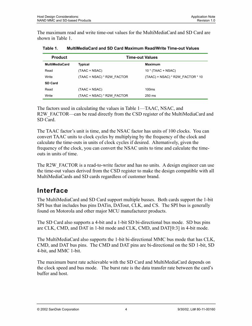
Host Design Considerations: Application Note NAND MMC and SD-based Products Revision 1.0
© 2002 SanDisk Corporation 4 9/30/02, Lit# 80-11-00160
The maximum read and write time-out values for the MultiMediaCard and SD Card are shown in Table 1.
Table 1. MultiMediaCard and SD Card Maximum Read/Write Time-out Values
Product Time-out Values MultiMediaCard Typical Maximum
Read (TAAC + NSAC) 10 * (TAAC + NSAC)
Write (TAAC + NSAC) * R2W_FACTOR (TAAC) + NSAC) * R2W_FACTOR * 10
SD Card Read (TAAC + NSAC) 100ms
Write (TAAC + NSAC) * R2W_FACTOR 250 ms
The factors used in calculating the values in Table 1—TAAC, NSAC, and R2W_FACTOR—can be read directly from the CSD register of the MultiMediaCard and SD Card. The TAAC factor’s unit is time, and the NSAC factor has units of 100 clocks. You can convert TAAC units to clock cycles by multiplying by the frequency of the clock and calculate the time-outs in units of clock cycles if desired. Alternatively, given the frequency of the clock, you can convert the NSAC units to time and calculate the time-outs in units of time. The R2W_FACTOR is a read-to-write factor and has no units. A design engineer can use the time-out values derived from the CSD register to make the design compatible with all MultiMediaCards and SD cards regardless of customer brand.
Interface The MultiMediaCard and SD Card support multiple busses. Both cards support the 1-bit SPI bus that includes bus pins DATin, DATout, CLK, and CS. The SPI bus is generally found on Motorola and other major MCU manufacturer products. The SD Card also supports a 4-bit and a 1-bit SD bi-directional bus mode. SD bus pins are CLK, CMD, and DAT in 1-bit mode and CLK, CMD, and DAT[0:3] in 4-bit mode. The MultiMediaCard also supports the 1-bit bi-directional MMC bus mode that has CLK, CMD, and DAT bus pins. The CMD and DAT pins are bi-directional on the SD 1-bit, SD 4-bit, and MMC 1-bit. The maximum burst rate achievable with the SD Card and MultiMediaCard depends on the clock speed and bus mode. The burst rate is the data transfer rate between the card’s buffer and host.
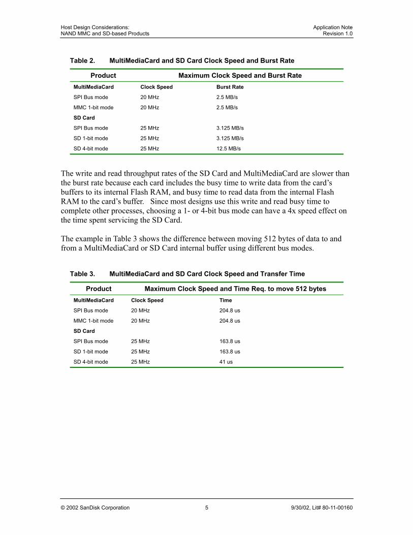
Host Design Considerations: Application Note NAND MMC and SD-based Products Revision 1.0
© 2002 SanDisk Corporation 5 9/30/02, Lit# 80-11-00160
Table 2. MultiMediaCard and SD Card Clock Speed and Burst Rate
Product Maximum Clock Speed and Burst Rate MultiMediaCard Clock Speed Burst Rate
SPI Bus mode 20 MHz 2.5 MB/s
MMC 1-bit mode 20 MHz 2.5 MB/s
SD Card SPI Bus mode 25 MHz 3.125 MB/s
SD 1-bit mode 25 MHz 3.125 MB/s
SD 4-bit mode 25 MHz 12.5 MB/s
The write and read throughput rates of the SD Card and MultiMediaCard are slower than the burst rate because each card includes the busy time to write data from the card’s buffers to its internal Flash RAM, and busy time to read data from the internal Flash RAM to the card’s buffer. Since most designs use this write and read busy time to complete other processes, choosing a 1- or 4-bit bus mode can have a 4x speed effect on the time spent servicing the SD Card. The example in Table 3 shows the difference between moving 512 bytes of data to and from a MultiMediaCard or SD Card internal buffer using different bus modes.
Table 3. MultiMediaCard and SD Card Clock Speed and Transfer Time
Product Maximum Clock Speed and Time Req. to move 512 bytes MultiMediaCard Clock Speed Time
SPI Bus mode 20 MHz 204.8 us
MMC 1-bit mode 20 MHz 204.8 us
SD Card SPI Bus mode 25 MHz 163.8 us
SD 1-bit mode 25 MHz 163.8 us
SD 4-bit mode 25 MHz 41 us
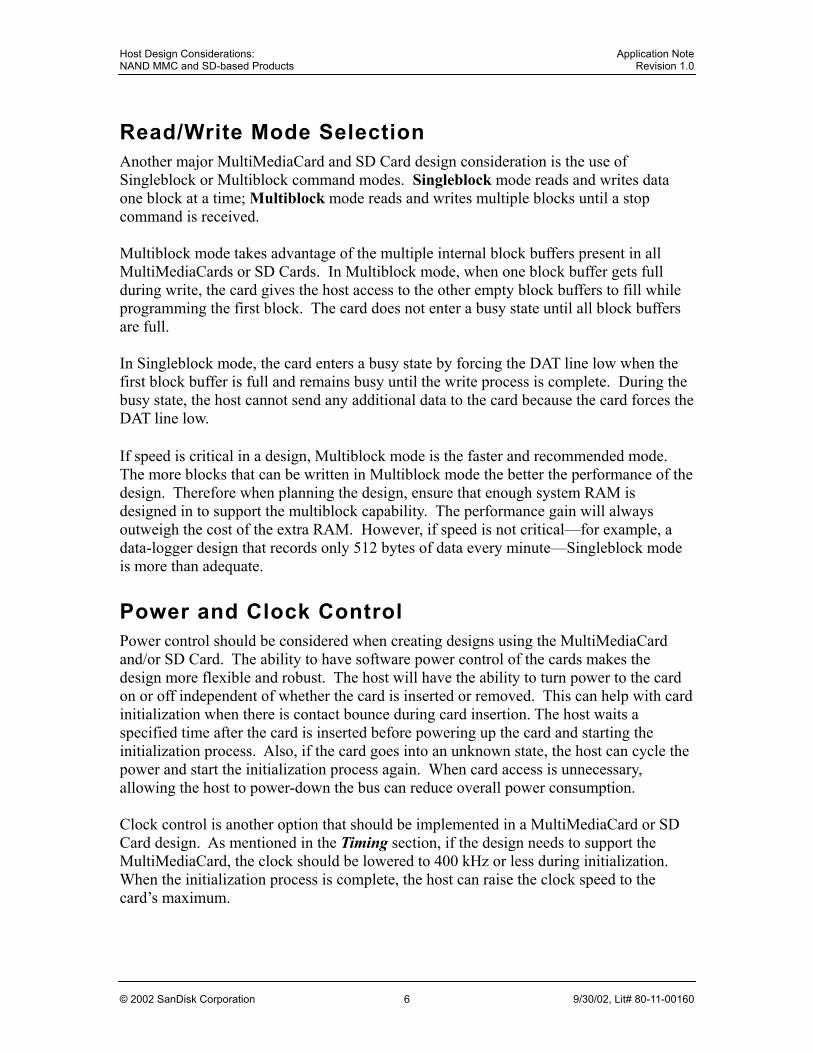
Host Design Considerations: Application Note NAND MMC and SD-based Products Revision 1.0
© 2002 SanDisk Corporation 6 9/30/02, Lit# 80-11-00160
Read/Write Mode Selection Another major MultiMediaCard and SD Card design consideration is the use of Singleblock or Multiblock command modes. Singleblock mode reads and writes data one block at a time; Multiblock mode reads and writes multiple blocks until a stop command is received. Multiblock mode takes advantage of the multiple internal block buffers present in all MultiMediaCards or SD Cards. In Multiblock mode, when one block buffer gets full during write, the card gives the host access to the other empty block buffers to fill while programming the first block. The card does not enter a busy state until all block buffers are full. In Singleblock mode, the card enters a busy state by forcing the DAT line low when the first block buffer is full and remains busy until the write process is complete. During the busy state, the host cannot send any additional data to the card because the card forces the DAT line low. If speed is critical in a design, Multiblock mode is the faster and recommended mode. The more blocks that can be written in Multiblock mode the better the performance of the design. Therefore when planning the design, ensure that enough system RAM is designed in to support the multiblock capability. The performance gain will always outweigh the cost of the extra RAM. However, if speed is not critical—for example, a data-logger design that records only 512 bytes of data every minute—Singleblock mode is more than adequate.
Power and Clock Control Power control should be considered when creating designs using the MultiMediaCard and/or SD Card. The ability to have software power control of the cards makes the design more flexible and robust. The host will have the ability to turn power to the card on or off independent of whether the card is inserted or removed. This can help with card initialization when there is contact bounce during card insertion. The host waits a specified time after the card is inserted before powering up the card and starting the initialization process. Also, if the card goes into an unknown state, the host can cycle the power and start the initialization process again. When card access is unnecessary, allowing the host to power-down the bus can reduce overall power consumption. Clock control is another option that should be implemented in a MultiMediaCard or SD Card design. As mentioned in the Timing section, if the design needs to support the MultiMediaCard, the clock should be lowered to 400 kHz or less during initialization. When the initialization process is complete, the host can raise the clock speed to the card’s maximum.
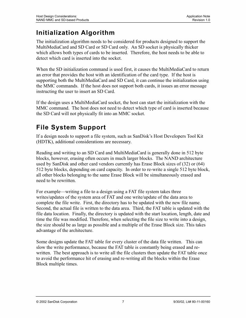
Host Design Considerations: Application Note NAND MMC and SD-based Products Revision 1.0
© 2002 SanDisk Corporation 7 9/30/02, Lit# 80-11-00160
Initialization Algorithm The initialization algorithm needs to be considered for products designed to support the MultiMediaCard and SD Card or SD Card only. An SD socket is physically thicker which allows both types of cards to be inserted. Therefore, the host needs to be able to detect which card is inserted into the socket. When the SD initialization command is used first, it causes the MultiMediaCard to return an error that provides the host with an identification of the card type. If the host is supporting both the MultiMediaCard and SD Card, it can continue the initialization using the MMC commands. If the host does not support both cards, it issues an error message instructing the user to insert an SD Card. If the design uses a MultiMediaCard socket, the host can start the initialization with the MMC command. The host does not need to detect which type of card is inserted because the SD Card will not physically fit into an MMC socket.
File System Support If a design needs to support a file system, such as SanDisk’s Host Developers Tool Kit (HDTK), additional considerations are necessary. Reading and writing to an SD Card and MultiMediaCard is generally done in 512 byte blocks, however, erasing often occurs in much larger blocks. The NAND architecture used by SanDisk and other card vendors currently has Erase Block sizes of (32) or (64) 512 byte blocks, depending on card capacity. In order to re-write a single 512 byte block, all other blocks belonging to the same Erase Block will be simultaneously erased and need to be rewritten. For example—writing a file to a design using a FAT file system takes three writes/updates of the system area of FAT and one write/update of the data area to complete the file write. First, the directory has to be updated with the new file name. Second, the actual file is written to the data area. Third, the FAT table is updated with the file data location. Finally, the directory is updated with the start location, length, date and time the file was modified. Therefore, when selecting the file size to write into a design, the size should be as large as possible and a multiple of the Erase Block size. This takes advantage of the architecture. Some designs update the FAT table for every cluster of the data file written. This can slow the write performance, because the FAT table is constantly being erased and re-written. The best approach is to write all the file clusters then update the FAT table once to avoid the performance hit of erasing and re-writing all the blocks within the Erase Block multiple times.