Embed Size (px)
Citation preview

1 INTRODUCTION
1.1 Overview of Dellin Semiconductor Tutorials
1.2 Overview of Core Competency Devices Course
2 SEMICONDUCTOR MATERIALS2.1 Semiconductor Materials2.2 Silicon2.3 Crystals2.4 Crystaline Silicon3 ELECTRONIC PROPERTIES3.1 Conduction and Valance Bands3.2 Electrons and Holes3.3 Generation and Recombination3.4 Intrinsic Semiconductors3.5 Currents4 DOPING: n AND p TYPE4.1 Doping: n and p Type4.2 Doping: More Details5 JUNCTIONS
5.1 Semiconductor Devices Are Made Up of Interfaces5.2 pn Junction with Zero External Bias5.3 Applying a Voltage to a pn Junction5.4 Other types of Junctions
6 TRANSISTORS6.1 MOS Capacitor6.2 MOS Transistor: Structure6.3 MOS Transistor: Operation6.4 Other Transistors Made in Silicon
6.5 Transistors Made in Other Semiconductors7 CMOS IC AND SCALING7.1 CMOS IC7.2 CMOS IC: Power and Performance
7.3 Scaling for Faster, Better, Cheaper ICs 8 PHOTODIODE AND SOLAR CELL8.1 Review of Optics
8.2 Photon Absorption in Semiconductors8.3 Photodiode
8.4 Solar Cell9 LED AND LASER DIODE
9.1 Spontaneous and Stimulated Emission
9.2 Semiconductor Junctions for Light Emission9.3 Light Emitting Diode (LED)9.4 Laser Diode: How It Works9.5 Edge‐Emitting Laser Diode & VCSEL
Core Competency In Semiconductor Technology:1. DEVICES
Dr. Theodore (Ted) DellinChief Scientist of the Microsystems Center (retired), Sandia National Labs
Reliability Lead (retired), Intl. Technology Roadmap for SemiconductorsQuick Start Micro Training LLC, [email protected], SemiconductorTutorials.com
© 2016, Dellin, All Rights Reserved.
SAMPLE SLIDES & COURSE OUTLINE
A Easy, Effective, Impactful Working Knowledge™ of Microelectronic & Optoelectronic Devices.Recommended for everyone who works with, or depends on, Semiconductor Technologies
Integrated With Our “Digging Deeper” courses in Semiconductor Devices if you need more detail.Integrated With Other Core Competency Courses: 2. Fabrication & 3. Reliability.
14 Hour CourseAvailable Learning Formats: Live, Webinar, Narrated eLearning, Course Notes & PowerPoint Slides.
DellinSemiconductor
Tutorials
Impactful Working Knowledge™Core Competency & Digging DeeperDevices, Fabrication & Reliability
For More Info: SemiconductorTutorials.com or email [email protected]

CORE COMPETENCY CERTIFICATIONIN SEMICONDUCTOR TECHNOLOGIES
DEVICETUTORIALS‐ Semiconductors‐ Junctions‐MOS Transistor‐ IC & Scaling‐ Photodiode & Solar Cell‐ LED and Laser
FABRICATIONTUTORIALS‐Microfabrication Techniques‐Making Devices‐ Packaging‐Micromachining & Microsystems
RELIABILITYTUTORIALS‐ Integrated Circuit and Component Reliability‐ CMOS IC Failure Mechanisms
INTEGRATED “DIGGING DEEPER” COURSESDEVICE‐ Semiconductors‐ Junctions‐ Transistor‐ Optoelectronics
FABRICATION‐ Unit Processes‐ CMOS IC Technology‐Materials
RELIABILITY‐ Failure Mechanisms‐ Rel Engineering‐ Prob. & Statistics
FORMATS
Narrated eLearning
Webinars
PowerPoint Slides
In‐Person Tutorials
UNIQUE FEATURES
Focused on real world needs of tech people
Easy to understand. Picture how things work instead of focusing on equations
Seamless integration of all tutorials
• Chief Scientist of Microsystems Research, Technology & Components Center, Sandia National Lab
• Reliability Lead International Technology Roadmap for Semiconductors
• Reliability Technical Advisory Board, Sematech
• External Review Panel, NASA NEPP
• Tech. & Genl. Chair, IEEE Nonvolatile Memory Technology Symposium
• FLC Award for Technology Transfer
• 6 Tutorials at IEEE Reliability Physics Symp.
• Unique training courses for industry & gov’t.
35 years experience in semiconductor technologies, reliability and training including:
DellinSemiconductor
Tutorials
Impactful Working Knowledge™Core Competency & Digging DeeperDevices, Fabrication & Reliability
For More Info: SemiconductorTutorials.com or email [email protected]

Sample SlidesSemiconductorTutorials.com©2016, Dellin, All Rights Reserved
DellinSemiconductorTutorials
Core Competency Tutorial: Semiconductor Devices
Dr. Ted Dellin
Dellin Semiconductor Tutorials, SemiconductorTutorials.com
Dellin Semiconductor TutorialsCD1: Introduction
Core Competency In-Depth
Devices Fabrication Reliability
CD2. SemiconductorMaterials
CD3. Electronic Properties
CD5. Junctions
CD6. Transistors
CD7. ICs and Scaling
CD8. Photodiode &Solar Cell
CD9. LED & Laser Diode
CD1. Introduction
CD4. Doping: n & p Type
1
1.1 Overview of Dellin Semiconductor Tutorials
1.2 Overview of Device Core Competency Tutorials Overview
Dellin Semiconductor Tutorials, SemiconductorTutorials.com
Dellin Semiconductor Tutorials StrategyFor Impactful Working Knowledge™
Intuitive Knowledge
Intuitive Knowledge
Intuitive Knowledge
BASIC CORE COMPETENCY
Devices-Fab-ReliabilityALL Technical Folks
IN-DEPTH EXPERTISESelected Folks in Selected Areas
Area 1Quantitative& Intuitive
Area 2Quantitative& Intuitive
TECHWORKFORCE
IMPACTFUL WORKING KNOWLEDGE™
2
Dellin Semiconductor Tutorials, SemiconductorTutorials.com
+VGS
- - - -S D
IMPACT•Evolutionary & Revolutionary Changes
•Analyze & Solve Problems•Flexibility in job assignments
m
VV
L
WCI thgoxeffsatds 2
)( 2
,
IMPACT•Derivation & Modeling•Prediction & Optimization
Intuitive Knowledge Quantitative Knowledge
Impactful Working Knowledge™
Impactful Working Knowledge™:Intuitive & Quantitative Knowledge
3
Dellin Semiconductor Tutorials, SemiconductorTutorials.com
Impactful Working Knowledge™
Dellin Semiconductor Tutorials Fills The Critical Need for Intuitive Knowledge
IntuitiveKnowledge
DellinSemiconductor
Tutorials
QuantitativeKnowledge
University Courses
4
Dellin Semiconductor Tutorials, SemiconductorTutorials.com
Areas Covered In ThisCore Competency Course
CMOS IC
Special Properties of Semiconductors
JunctionsMOS Capacitor
MOSTransistor
Bipolar& Other
Transistors
PhotodetectorSolar Cell
LED &LaserDiode
CMOS Technology
MEMS
Microsystem
Optics
Semiconductor Processing Techniques
ReliabilityEngineering
IC FailureMechanisms
IC Industry
Scaling CMOS
Process Flow
5
Dellin Semiconductor Tutorials, SemiconductorTutorials.com
Course Goals:Core Competency: Devices
• Impactful Working Knowledge™ needed by all people working with, or dependent on, semiconductor devices
• Intuitive Understanding (“Picturing How Devices Work”)
– Complements University-type courses that focus on Quantitative Understanding
• Present the knowledge in an effective, efficient, easy-to-understand and engaging manner
• (If needed) Solid foundation for our “Digging Deeper” courses in Devices
6

Sample SlidesSemiconductorTutorials.com©2016, Dellin, All Rights Reserved
DellinSemiconductorTutorials
Core Competency Tutorial: Semiconductor Devices
Dr. Ted Dellin
Dellin Semiconductor Tutorials, SemiconductorTutorials.com
Dellin Semiconductor TutorialsCD2: Semiconductor Materials
Core Competency In-Depth
Devices Fabrication Reliability
CD2. SemiconductorMaterials
CD3. Electronic Properties
CD5. Junctions
CD6. Transistors
CD7. ICs and Scaling
CD8. Photodiode &Solar Cell
CD9f. LED & Laser Diode
CD1. Introduction
CD4. Doping: n & p Type
7
2.1 Semiconductor Materials
2.2 Silicon
2.3 Crystalline Semiconductors
2.4 Crystalline Silicon
Dellin Semiconductor Tutorials, SemiconductorTutorials.com
Three Important Characteristicsof Semiconductors
Semiconductor
• Separation between valance & conduction bands
• Larger bandgap = higher operating temperature
• Determines colors of light absorbed & emitted
1. BANDGAP ENERGY
• Only direct semiconductors are efficient light emitters (e.g., LEDs)
2. DIRECT OR INDIRECT BANDGAP
• Distance between atoms in crystal
• Determines which crystals can be grown on top of each other with minimum defects
3. CRYSTAL LATTICE CONSTANT
Dellin Semiconductor Tutorials, SemiconductorTutorials.com
Why Is Silicon The Dominant Semiconductor For Integrated Circuits?
• Silicon is the only semiconductor
– With a very robust oxide
– On which we can grow a very good oxide/semiconductor interface
• This makes Silicon the best choice for MOS transistors
– MOS transistors are the best choice for almost all ICs
• Also a good choice for high density bipolar ICs
Silicon
Silicon Dioxide
9
Dellin Semiconductor Tutorials, SemiconductorTutorials.com
Amorphous, Polycrystalline and Crystalline Semiconductors Attributes
AMORPHOUS CRYSTALLINEPOLYCRYSTALLINE
Better Performance
Lower Cost
Larger Area Devices
10
Dellin Semiconductor Tutorials, SemiconductorTutorials.com
Why Si Wafers with (100) Surfaces?Why Align IC Edges along [110] Directions?
• Transistors formed on (100) surfaces were found to have less trapped charges at the oxide/silicon interface which leads to better transistors.
• The FCC cubic crystal structure naturally fractures along [110] directions. By orienting the ICs edges along [110] directions any cracks formed during the cutting out of the die will tend to go along the saw line, not across the IC Courtesy of Micron
<110> Directions
11
Dellin Semiconductor Tutorials, SemiconductorTutorials.com
The Diamond Lattice (e.g., Silicon)
• Two intersecting face centered cubic lattices– Both lattices contain the
same silicon atoms (the open and shaded circles in the figure are Si atoms)
• Cube side = 0.54nm
.54 nm Both are the same Si atom
12

Sample SlidesSemiconductorTutorials.com©2016, Dellin, All Rights Reserved
DellinSemiconductorTutorials
Core Competency Tutorial: Semiconductor Devices
Dr. Ted Dellin
Dellin Semiconductor Tutorials, SemiconductorTutorials.com
Dellin Semiconductor TutorialsCD3: Semi Electronic Properties
Core Competency In-Depth
Devices Fabrication Reliability
3.1 Conduction & Valence Bands
3.2 Electrons & Holes
3.3 Generation and Recombination
3.4 Intrinsic Semiconductors
3.5 Currents
CD2. SemiconductorMaterials
CD3. Electronic Properties
CD5. Junctions
CD6. Transistors
CD7. ICs and Scaling
CD8. Photodiode &Solar Cell
CD9. LED & Laser Diode
CD1. Introduction
CD4. Doping: n & p Type
13
Dellin Semiconductor Tutorials, SemiconductorTutorials.com
In The Semiconductor CrystalWe Only Have To Consider Two Bands
T = 0K (Absolute Zero)
Higher-Energy “Conduction” Band
Band GapNo Allowed Electron States
EL
EC
TR
ON
EN
ER
GY
Lower-Energy “Valence” Band
= Empty electron energy state = Energy state filled with an electron
# states = # valence electrons
14
Dellin Semiconductor Tutorials, SemiconductorTutorials.com
Generation of an Electron/Hole Pair
• Thermal or light can break the bond that binds the valence electron to the Si atom
Conduction Electron
Si Si Si Si
Si Si Si Si
Si Si Si Si
“Hole”(Missing Valence
Electron)
• If enough energy is supplied a “free” negative electron is created that can move through the crystal (conduction band)
• The site of the missing bonding electron (called a “hole”) has a net positive charge
15
Dellin Semiconductor Tutorials, SemiconductorTutorials.com
Recombination (Loss of an Electron/Hole Pair) Releases Energy
Heat(Crystal Lattice Vibration –Phonon)
Photon of Light(Semiconductor LEDs and Laser Diodes)
Rate of
Recombination
# of
Electrons
# of
Holes
~ X
16
Dellin Semiconductor Tutorials, SemiconductorTutorials.com
Intrinsic Carrier Concentration Increases With Decreasing Bandgap
100 200 300 400 50010 20
10 15
10 10
10 5
1
510
1010
1015
GeSi
GaAs
Temperature (K)
Material Band Gap (eV)
Room Temp. Intrinsic Carrier Concen-tration (1010/cm3)
Ge 0.66 200
Si 1.12 1
GaAs 1.42 0.00042
17
Dellin Semiconductor Tutorials, SemiconductorTutorials.com
Mobilities For Different Semiconductors
Values given are representative
0.1
1
10
100
1000
10000
100000
Organic Semiconductors
GeGaAs
InAs
Amorphous Si
Crystalline SiliconBulk Surface Strained
Surface
Mo
bili
ty (
cm2/V
s)
Electron
Hole
18

Sample SlidesSemiconductorTutorials.com©2016, Dellin, All Rights Reserved
DellinSemiconductorTutorials
Core Competency Tutorial: Semiconductor Devices
Dr. Ted Dellin
Dellin Semiconductor Tutorials, SemiconductorTutorials.com
Dellin Semiconductor TutorialsCD4: Doping: n and p Type
Core Competency In-Depth
Devices Fabrication Reliability
4.1 Doping to Make n and p Type
4.2 Doping: More Details
CD2. SemiconductorMaterials
CD3. Electronic Properties
CD5. Junctions
CD7. Transistors
CD6. ICs and Scaling
CD8. Photodiode &Solar Cell
CD9. LED & Laser Diode
CD1. Introduction
CD4. Doping: n & p Type
19
Dellin Semiconductor Tutorials, SemiconductorTutorials.com
Intrinsic
“Doping” With Dopant Atoms to Make Electron-rich n Type or Hole-rich p Type
• Add “acceptor” atoms with one lessvalence electron
• Lots of holes (controlled by # of acceptor atoms)
• - B acceptor ions
• Very few electrons
• Pure semiconductor
• Small, equal number of mobile holes and electrons
+
-
+
-
• Add “donor” atoms with extra valence electron
• Lots of electrons (controlled by # of donor atoms)
• + P “donor” ions
• Very few holes
n Type
+
-P+ P+ P+ P+ P+
- - - --
p Type
B- B- B- B- B-
-
+ + + + ++
EC
EV
20
Dellin Semiconductor Tutorials, SemiconductorTutorials.com
n Type
+
-P+ P+ P+ P+ P+
- - - --
Majority Carrier:
Electrons
Minority Carrier:Holes
p Type
B- B- B- B- B-
-
+ + + + ++
Minority Carrier:
Electrons
Majority Carrier:Holes
Definition of Majority and Minority Carriers
21
Dellin Semiconductor Tutorials, SemiconductorTutorials.com
Compensation (Counter Doping) Can Turn p Type Into n Type (or vice versa)
B-
B-B-
B-
B-
+
+++
+ P+
P+ P+P+
P+
p Type
B AtomsMake Si
hole-rich p Type
Adding a Higher Concentration of P Atoms Into A Region Turns
It IntoElectron-rich n Type
-
n Type- -
B-
B- B-
B-+
++
+
p Type
B-
22
Dellin Semiconductor Tutorials, SemiconductorTutorials.com
At Higher Dopant LevelsSemiconductors are Degenerate
P
Conduction Band
P P P P P P
Nondegenerate Degenerate
• Higher doping levels (>1018 /cm3)
• Dopant atoms interact. Energy levels split due to Pauli exclusion principle
• Dopant energy levels form “subband” under conduction band edge
• Makes the bandgap energy appear smaller
Valence Band
EG“Apparent”
EG
23
Dellin Semiconductor Tutorials, SemiconductorTutorials.com
Controlling the # of Donor Atoms Controls The # of Electrons & Holes in n Type
# electrons= # donor
atoms
# holes depends on # of donor
atoms and temperature
Similarly, we can control the electrons and holes in a p type semiconductor by controlling the number of acceptor atoms
Light (n-)(1015 Dopants/cm3)
1015
electrons/cm3
105
holes/cm3
(Room temp.)
Medium (n)(1017 Dopants/cm3)
1017
electrons/cm3
103
holes/cm3
(Room temp.)
Heavy (n+)(1019 Dopants/cm3)
1019
electrons/cm3
10holes/cm3
(Room temp.)
24
Sample SlidesSemiconductorTutorials.com©2016, Dellin, All Rights Reserved
DellinSemiconductorTutorials
Core Competency Tutorial: Semiconductor Devices
Dr. Ted Dellin
Dellin Semiconductor Tutorials, SemiconductorTutorials.com
Dellin Semiconductor TutorialsCD5: Junctions
Core Competency In-Depth
Devices Fabrication Reliability
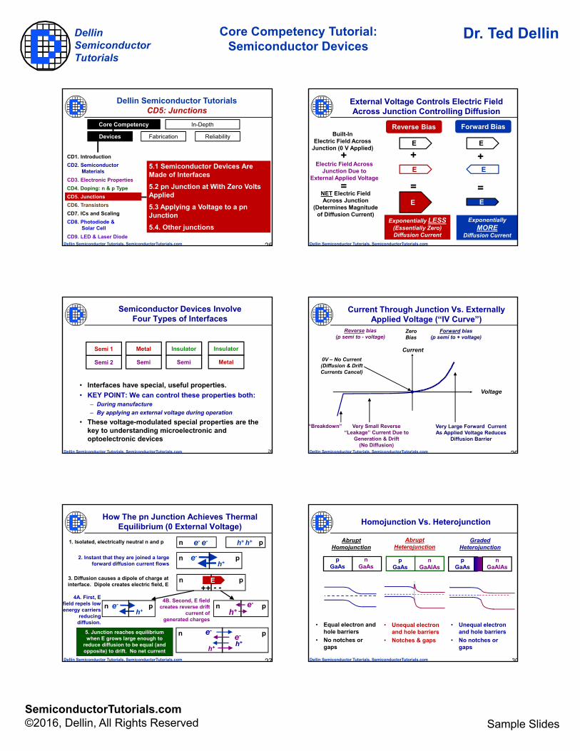
5.1 Semiconductor Devices Are Made of Interfaces
5.2 pn Junction at With Zero Volts Applied
5.3 Applying a Voltage to a pn Junction
5.4. Other junctions
CD2. SemiconductorMaterials
CD3. Electronic Properties
CD5. Junctions
CD6. Transistors
CD7. ICs and Scaling
CD8. Photodiode &Solar Cell
CD9. LED & Laser Diode
CD1. Introduction
CD4. Doping: n & p Type
25
Dellin Semiconductor Tutorials, SemiconductorTutorials.com
Semiconductor Devices InvolveFour Types of Interfaces
• Interfaces have special, useful properties.
• KEY POINT: We can control these properties both:– During manufacture
– By applying an external voltage during operation
• These voltage-modulated special properties are the key to understanding microelectronic and optoelectronic devices
Semi 1
Semi 2
Metal
Semi
Insulator
Semi
Insulator
Metal
26
Dellin Semiconductor Tutorials, SemiconductorTutorials.com
How The pn Junction Achieves Thermal Equilibrium (0 External Voltage)
n pe- e- h+ h+1. Isolated, electrically neutral n and p
n p++ - -
E3. Diffusion causes a dipole of charge at interface. Dipole creates electric field, E
2. Instant that they are joined a large forward diffusion current flows h+
e-n p
h+e-n p
4A. First, E field repels low energy carriers
reducing diffusion.
n pe-
h+
4B. Second, E field creates reverse drift
current of generated charges
n pe-
h+h+
e-5. Junction reaches equilibrium when E grows large enough to
reduce diffusion to be equal (and opposite) to drift. No net current
27
Dellin Semiconductor Tutorials, SemiconductorTutorials.com
External Voltage Controls Electric Field Across Junction Controlling Diffusion
E
Reverse Bias Forward Bias
EBuilt-In
Electric Field Across Junction (0 V Applied)
Exponentially LESS(Essentially Zero)Diffusion Current
ExponentiallyMORE
Diffusion Current
E
+E
+Electric Field Across
Junction Due to External Applied Voltage
+
E
=E
=NET Electric Field Across Junction
(Determines Magnitude of Diffusion Current)
=
Dellin Semiconductor Tutorials, SemiconductorTutorials.com
Voltage
Current
Forward bias(p semi to + voltage)
ZeroBias
Current Through Junction Vs. Externally Applied Voltage (“IV Curve”)
Reverse bias(p semi to - voltage)
“Breakdown” Very Small Reverse“Leakage” Current Due to
Generation & Drift(No Diffusion)
Very Large Forward CurrentAs Applied Voltage Reduces
Diffusion Barrier
0V – No Current(Diffusion & Drift Currents Cancel)
29
Dellin Semiconductor Tutorials, SemiconductorTutorials.com
Homojunction Vs. Heterojunction
p GaAs
n GaAs
Abrupt Homojunction
p GaAs
n GaAlAs
Abrupt Heterojunction
• Unequal electron and hole barriers
• Notches & gaps
p GaAs
n GaAlAs
GradedHeterojunction
• Unequal electron and hole barriers
• No notches or gaps
• Equal electron and hole barriers
• No notches or gaps
30

Sample SlidesSemiconductorTutorials.com©2016, Dellin, All Rights Reserved
DellinSemiconductorTutorials
Core Competency Tutorial: Semiconductor Devices
Dr. Ted Dellin
Dellin Semiconductor Tutorials, SemiconductorTutorials.com
Dellin Semiconductor TutorialsCD6: Transistors
Core Competency In-Depth
Devices Fabrication Reliability
6.1 MOS Capacitor
6.2 MOS Transistor: Structure
6.3 MOS Transistor: Operation
6.4 Other Types of Transistors Made in Silicon
6.5 Transistors Made in Other Semiconductors
6.6 Other Transistors
CD2. SemiconductorMaterials
CD3. Electronic Properties
CD5. Junctions
CD6. Transistors
CD7. ICs and Scaling
CD8. Photodiode &Solar Cell
CD9. LED & Laser Diode
CD1. Introduction
CD4. Doping: n & p Type
31
Dellin Semiconductor Tutorials, SemiconductorTutorials.com
The Field Effect: Using a Voltage To Turn The Surface of a p Type Semi into n Type
+
+
+
+
+
+
+
++
+
++
+
+
+
VGATE = 0“Metal”
Gate
Oxide
p Type Semi-
conductor
0 Volts
-
+
+
+
+
--
+
++
+
- - -
+VGATE > VTHRESHOLD
Thin “inversion” layer of electron-rich n type
0 Volts
+ -Hole Electron
0 Gate Voltage Gate Voltage Above Threshold
32
Dellin Semiconductor Tutorials, SemiconductorTutorials.com
Scanning Electron MicroscopeCross Section of MOS Transistor
SEM: Mike Strizich, Analytical Solutions
Polysilicon Gate
Oxide(too thin to be seen)
Surface of Silicon Wafer
Drain (n type)
Source (n type)
p Well
33
Dellin Semiconductor Tutorials, SemiconductorTutorials.com
Increasing Drain Voltage Has A Limited Ability To Increase Current
Average Speed of Electrons
Across The Channel
(Determines Current)
VDSAT
DrainVoltage
Current ~ electron velocity ~ (Mobility)(Electric Field)
Increasing VD
increases E Field Along Channel
For VD > VDSAT channel is pinched off. Increasing VD
does NOT increase E Field, or velocity.
Current saturates.
34
Dellin Semiconductor Tutorials, SemiconductorTutorials.com
Storage or Absence of Electrons on Floating Gate Determines “0” or “1”
• Higher than normal voltages used to add or remove electrons from floating gate
• “0” or “1” determined by higher or lower transistor currents due to presence or absence of electrons on FG
• Nonvolatile Memory: electrons are trapped - will retain high or low threshold without power being applied
n n
Control Gate
Floating Gate
n n
e- e- e- e-
Uncharged Floating GateHigher Current
Charged Floating GateLower Current
Dellin Semiconductor Tutorials, SemiconductorTutorials.com
High Electron Mobility Transistor(HEMT, Also Called MODFET)
Source Gate Drain
Semi-insulating GaAs
Undoped GaAs
n AlGaAs Quantum Well at Interface That
Traps Electrons
Acts as the Transistor’s
Channel
n++ n++
36
• Quantum energy well formed in top surface of undoped GaAs
• Lots of electrons from n AlGaAs
• Very little scattering in channel
• Advantages: High speed and low noise
Sample SlidesSemiconductorTutorials.com©2016, Dellin, All Rights Reserved
DellinSemiconductorTutorials
Core Competency Tutorial: Semiconductor Devices
Dr. Ted Dellin
Dellin Semiconductor Tutorials, SemiconductorTutorials.com
Dellin Semiconductor TutorialsCD7: ICs and Scaling
Core Competency In-Depth
Devices Fabrication Reliability
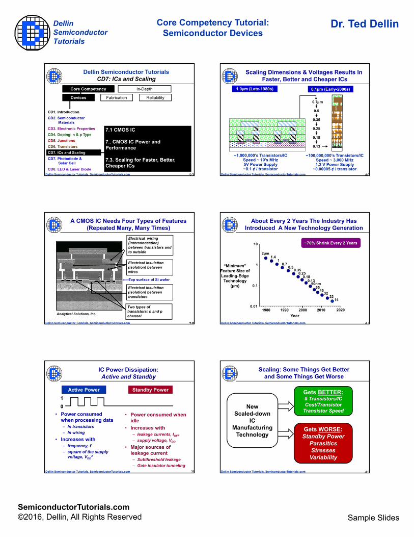
7.1 CMOS IC
7.. CMOS IC Power and Performance
7.3. Scaling for Faster, Better, Cheaper ICs
CD2. SemiconductorMaterials
CD3. Electronic Properties
CD5. Junctions
CD6. Transistors
CD7. ICs and Scaling
CD7. Photodiode &Solar Cell
CD8. LED & Laser Diode
CD1. Introduction
CD4. Doping: n & p Type
37
Dellin Semiconductor Tutorials, SemiconductorTutorials.com
A CMOS IC Needs Four Types of Features (Repeated Many, Many Times)
Electrical insulation (isolation) between transistors
Electrical wiring (interconnection) between transistors and to outside
Two types of transistors: n and p channel
Electrical insulation (isolation) between wires
Top surface of Si wafer
Analytical Solutions, Inc.
38
Dellin Semiconductor Tutorials, SemiconductorTutorials.com
IC Power Dissipation:Active and Standby
• Power consumed when processing data– In transistors
– In wiring
• Increases with– frequency, f
– square of the supply voltage, VDD
2
• Power consumed when idle
• Increases with– leakage currents, IOFF
– supply voltage, VDD
• Major sources of leakage current– Subthreshold leakage
– Gate insulator tunneling
Active Power Standby Power
0
1
39
Dellin Semiconductor Tutorials, SemiconductorTutorials.com
Scaling Dimensions & Voltages Results In Faster, Better and Cheaper ICs
~100,000,000’s Transistors/ICSpeed ~ 3,000 MHz1.2 V Power Supply
~0.00005 ¢ / transistor
~1,000,000’s Transistors/ICSpeed ~ 10’s MHz5V Power Supply~0.1 ¢ / transistor
0.7m
0.35
0.25
0.18
0.13
0.5
1.0µm (Late-1980s) 0.1µm (Early-2000s)
40
Dellin Semiconductor Tutorials, SemiconductorTutorials.com
About Every 2 Years The Industry Has Introduced A New Technology Generation
~70% Shrink Every 2 Years
Year
0.01
0.1
1
10
1980 1990 2000 2010
“Minimum” Feature Size of Leading-Edge Technology
(µm)
2020
2µm
45
22
1.41
0.70.5
0.350.25
0.180.13
90nm65
32
14
41
Dellin Semiconductor Tutorials, SemiconductorTutorials.com
Scaling: Some Things Get Better and Some Things Get Worse
NewScaled-down
IC Manufacturing
Technology
Gets BETTER:# Transistors/ICCost/Transistor
Transistor Speed
Gets WORSE:Standby Power
ParasiticsStresses
Variability
42
Sample SlidesSemiconductorTutorials.com©2016, Dellin, All Rights Reserved
DellinSemiconductorTutorials
Core Competency Tutorial: Semiconductor Devices
Dr. Ted Dellin
Dellin Semiconductor Tutorials, SemiconductorTutorials.com
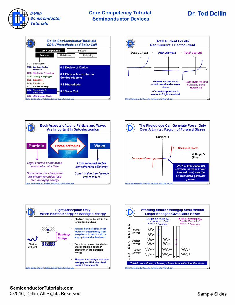
Dellin Semiconductor TutorialsCD8: Photodiode and Solar Cell
Core Competency In-Depth
Devices Fabrication Reliability
8.1 Review of Optics
8.2 Photon Adsorption in Semiconductors
8.3 Photodiode
8.4 Solar Cell
CD2. SemiconductorMaterials
CD3. Electronic Properties
CD5. Junctions
CD6. Transistors
CD7. ICs and Scaling
CD8. Photodiode &Solar Cell
CD9. LED & Laser Diode
CD1. Introduction
CD4. Doping: n & p Type
43
Dellin Semiconductor Tutorials, SemiconductorTutorials.com
Both Aspects of Light, Particle and Wave, Are Important in Optoelectronics
Optoelectronics WaveParticle
Light emitted or absorbed one photon at a time
No emission or absorption for photon energies less
than bandgap energy
Light reflected and/or bent affecting efficiency
Constructive interference key to lasers
44
Dellin Semiconductor Tutorials, SemiconductorTutorials.com
Light Absorption Only When Photon Energy >= Bandgap Energy
-
- - - - - -- - - - -Photon
of Light
-+
-
Bandgap Energy
• Electron cannot be within the forbidden bandgap
• Valence band electron must receive enough energy from one photon to make it all the way up to conduction band
• For this to happen the photon energy must be equal or greater than the bandgap energy
• Photons with energy less than bandgap are NOT absorbed (semi is transparent)
45
Dellin Semiconductor Tutorials, SemiconductorTutorials.com
Total Current Equals Dark Current + Photocurrent
I
Dark Current Photocurrent+
I
•Reverse current under both forward and reverse
biases
• Current proportional to amount of light absorbed
I
= Total Current
V
• Light shifts the Dark Current IV curve
downward
46
Dellin Semiconductor Tutorials, SemiconductorTutorials.com
The Photodiode Can Generate Power Only Over A Limited Region of Forward Biases
Current, I
Voltage, V(Bias)
Only in this quadrant (reverse current under forward bias) can the photodiodes generate
power
Consumes Power
Consumes Power
47
Dellin Semiconductor Tutorials, SemiconductorTutorials.com
Stacking Smaller Bandgap Semi Behind Larger Bandgap Gives More Power
p n
Smaller Bandgap EG2Smaller VMAX2 (~EG2)Power2 = VMAX2 IMAX2
Larger Bandgap EG1Larger VMAX1 (~EG1)Power1 = VMAX1 IMAX1
p n
HigherEnergy
MediumEnergy
LowerEnergy
SOLAR
PHOTONS
Total Power = Power1 + Power2 > Power from either junction alone
48

Sample SlidesSemiconductorTutorials.com©2016, Dellin, All Rights Reserved
DellinSemiconductorTutorials
Core Competency Tutorial: Semiconductor Devices
Dr. Ted Dellin
Dellin Semiconductor Tutorials, SemiconductorTutorials.com
Dellin Semiconductor TutorialsCD9: LED & Laser Diode
Core Competency In-Depth
Devices Fabrication Reliability
9.1 Spontaneous & Stimulated Emission
9.2 Semiconductor Junctions for Light Emission
9.3 Light Emitting Diode (LED)
9.4 Laser Diode: How it Works
9.5 Edge-Emitting Laser Diode and VCSEL
CD2. SemiconductorMaterials
CD3. Electronic Properties
CD5. Junctions
CD6. Transistors
CD7. ICs and Scaling
CD8. Photodiode &Solar Cell
CD9. LED & Laser Diode
CD1. Introduction
CD4. Doping: n & p Type
49
Dellin Semiconductor Tutorials, SemiconductorTutorials.com
2. Stimulated Emission
• Requires an incident photon that exactly matches the energy difference between the electron and the hole
• Stimulates emission of a second photon as first photon passes
– Emitted photon has same energy, direction and phase as incident photon
• Result is photon amplification (leads to lasers)
• Rate depends on both electron/hole and photon concentrations
+- - - - - -- - - - -
-
IncidentPhoton Incident
Photon
EmittedPhoton
50
Dellin Semiconductor Tutorials, SemiconductorTutorials.com
Double Heterojunctions Are Good For Photon Emission
1. Barriers keep electrons and holes in middle layer longer resulting in a larger fraction
recombining to make photons
2. Added benefit: Wide bandgap materials will not absorb lower energy photons from narrow
band gap
Narrow Bandgap pWide Bandgap p Wide Bandgap n+V -V
51
Dellin Semiconductor Tutorials, SemiconductorTutorials.com
Light Output of an LED Controlled by Current Across Junction
LightPowerOutput
Current Across Junction
Light Power ~ Current
Thermal Roll Off
52
Dellin Semiconductor Tutorials, SemiconductorTutorials.com
What Is Going On Inside A Semiconductor Laser When It Is Lasing?
• Photons are concentrated into a single beam– Single direction (perpendicular to side reflectors)
– Single energy• Concentration of photon beam is so great that all electrons and
holes injected immediately undergo stimulated emission producing more photons in that single direction and single energy
– Stimulated emission at other energies and/or directions and/or spontaneous emission doesn’t have a chance
• The electron/hole current injected is so large that the photon beam is amplified as it crosses the semiconductor
Semiconductor
53
Dellin Semiconductor Tutorials, SemiconductorTutorials.com
VCSEL FIB Cross Section
Oxidized MESA edge
OutputFacet
p-contactmetal
Dan Barton, Sandia
Top DBR (Dielectric
Mirror)
Bottom DBR (Dielectric
Mirror)
Optical CavityLight Emission
54