Embed Size (px)
Citation preview

Chipsmall Limited consists of a professional team with an average of over 10 year of expertise in the distribution
of electronic components. Based in Hongkong, we have already established firm and mutual-benefit business
relationships with customers from,Europe,America and south Asia,supplying obsolete and hard-to-find components
to meet their specific needs.
With the principle of “Quality Parts,Customers Priority,Honest Operation,and Considerate Service”,our business
mainly focus on the distribution of electronic components. Line cards we deal with include
Microchip,ALPS,ROHM,Xilinx,Pulse,ON,Everlight and Freescale. Main products comprise
IC,Modules,Potentiometer,IC Socket,Relay,Connector.Our parts cover such applications as commercial,industrial,
and automotives areas.
We are looking forward to setting up business relationship with you and hope to provide you with the best service
and solution. Let us make a better world for our industry!
Contact usTel: +86-755-8981 8866 Fax: +86-755-8427 6832
Email & Skype: [email protected] Web: www.chipsmall.com
Address: A1208, Overseas Decoration Building, #122 Zhenhua RD., Futian, Shenzhen, China

S6BP401A
Power Management IC for Automotive ADAS Platform
Cypress Semiconductor Corporation • 198 Champion Court • San Jose, CA 95134-1709 • 408-943-2600 Document Number: 002-03341 Rev.*C Revised August 9, 2016
Quad Buck 2.1 MHz DC/DC Converter and Dual LDO with Watchdog Timer
S6BP401A is a power management IC, consists of quad buck 2.1 MHz DC/DC converter with built-in switching FETs, dual Low
Drop-out regulator (LDOs) and a digital windowed watchdog timer. Having the switching FETs built-in, S6BP401A realizes high
power conversion efficiency and high switching frequency up to 2.4 MHz. The internal FETs are capable to handle up to 3A load. As
S6BP401A employs the current mode architecture, it has fast load transient response. Built-in output voltage setting resistors and
compensation circuits reduce BOM cost and component area.
Features
Quad Buck DC/DC Converter (DD1 to DD4)
VIN Input Range: 4.5V to 5.5V
Switching Frequency
External clock mode: 1.8 MHz to 2.4 MHz
Internal clock mode: 2.0 MHz to 2.2 MHz
Built-in Switching FETs up to 3A
Built-in Output Voltage Setting Resistors
Built-in Compensation Circuits
Dual LDO (LD1, LD2)
VIN Input Voltage Range: 2.97V to 5.5V
Built-in Output Voltage Setting resistors
Power Good Monitor Output for each DC/DC Converters, LDOs
Built-in Windowed Watchdog Timer (WDT)
Under Voltage Lockout (UVLO)
Thermal Shutdown (TSD)
Over Current Protection (OCP)
Over Voltage Protection (OVP)
Independent Enabling for each DC/DC Converters and LDOs
Load-independent Soft-Start
Built-in Discharge Resistors
Small 6 mm × 6 mm QFN-40 Package
AEC-Q100 compliant (Grade-1)
Applications
Automotive Applications
Advanced Driver Assistance Systems (ADAS)
Camera Systems such as Security Camera
Industrial Applications
Block Diagram
5
1.20V~1.575V / 2A
1.00V~1.275V / 3A
1.20V~2.575V / 2A
3.3V~3.4V / 1A
3.3V~3.4V / 0.2A
1.20V~2.875V / 0.5A
S6BP401A : PMIC
5V
DC/DC converter
LDO
Power Good
Watch Dog

Document Number: 002-03341 Rev.*C Page 2 of 38
S6BP401A
More Information
Cypress provides a wealth of data at www.cypress.com/pmic to help you to select the right PMIC device for your design, and to help
you to quickly and effectively integrate the device into your design. Following is an abbreviated list for S6BP401A:
Overview: Automotive PMIC Portfolio, Automotive PMIC Roadmap
Product Selector:
S6BP401A: 6ch Automotive PMIC for ADAS
Application Notes: Cypress offers S6BP401A application notes. Recommended application notes for getting started with S6BP401A are:
AN98649: How to Design a Power Management System
AN201006: Thermal Considerations and Parameters
Evaluation Kit Operation Manual:
S6SBP401AM2SA1001: Power block for automotive ADAS platform
Related Products:
S6BP201A, S6BP202A, S6BP203A:
1ch Buck-Boost Automotive PMIC
S6BP501A, S6BP502A:
3ch Automotive PMIC for Instrument Cluster
Contents Features ................................................................................................................................................................................... 1
Applications ............................................................................................................................................................................ 1
Block Diagram......................................................................................................................................................................... 1
More Information .................................................................................................................................................................... 2
1. Typical Application ........................................................................................................................................................ 3
2. Pin Configuration ........................................................................................................................................................... 4
3. Pin Functions ................................................................................................................................................................. 5
4. Preset Output Voltage.................................................................................................................................................... 6
5. Architecture Block Diagram .......................................................................................................................................... 8
6. Absolute Maximum Ratings ........................................................................................................................................ 10
7. Recommended Operating Conditions ........................................................................................................................ 11
8. Electrical Characteristics ............................................................................................................................................ 12
9. Operating Mode List..................................................................................................................................................... 17
10. Function ........................................................................................................................................................................ 18
10.1 Turning ON and OFF Sequence .................................................................................................................................. 18
10.2 Over Current Protection ............................................................................................................................................... 20
10.3 Over Voltage Protection .............................................................................................................................................. 20
10.4 Thermal Shutdown (TSD) ............................................................................................................................................ 21
10.5 Under Voltage Lockout (UVLO) ................................................................................................................................... 21
10.6 Soft-Start Operation..................................................................................................................................................... 21
10.7 Discharge Operation.................................................................................................................................................... 22
10.8 Power Good Monitor and Reset Function .................................................................................................................... 23
10.9 Watchdog Timer .......................................................................................................................................................... 25
10.10 Internal Linear Regulator Output (VREG) .................................................................................................................... 28
11. Application Circuit Example ........................................................................................................................................ 29
12. Reference Data ............................................................................................................................................................. 31
13. Ordering Information ................................................................................................................................................... 34
14. Package Dimensions ................................................................................................................................................... 35
15. Major Changes ............................................................................................................................................................. 36
Document History ................................................................................................................................................................. 36
Sales, Solutions, and Legal Information ............................................................................................................................. 38
Document Number: 002-03341 Rev.*C Page 3 of 38
S6BP401A
1. Typical Application
Figure 1-1 Typical Application

Document Number: 002-03341 Rev.*C Page 4 of 38
S6BP401A
2. Pin Configuration
Figure 2-1 Pin Configuration
PG
L2
GN
D
LD
O2
PV
CC
L2
PV
CC
L1
LD
O1
VC
C
PG
1
VR
EG
PG
2
PG4 FB1
FB4 PVCC1
PVCC4 LX1
LX4 PGND1
PGND4 PGND2
PGND3 PGND2
LX3 LX2
PVCC3 LX2
FB3 PVCC2
PG3 PVCC2
SY
NC
WD
I
RS
T
EN
L2
EN
L1
EN
4
EN
3
EN
2
EN
1
FB
2
(Corner Pad)
(Corner Pad) (Corner Pad)
(Corner Pad)CP1 CP4
CP3CP2 17 18 19 2011 12 13 14 15 16
8 23
9 22
10 21
1
7 24
2Top View
29
3 28
4 27
5 26
EP (Exposed Pad)6 25
30
40 39 38 37 36 35 34 33 32 31

Document Number: 002-03341 Rev.*C Page 5 of 38
S6BP401A
3. Pin Functions
Table 3-1 Pin Functions
Functional Block
Pin Number Pin Name I/O Description Pin Setting When Not Being Used
DD1
19 EN1 I Enable input terminal of DD1. Ground
30 FB1 I Output voltage feedback terminal of DD1. Ground
33 PG1 O Power good output terminal of DD1. Ground
29 PVCC1 - Power supply terminal of DD1. VCC
28 LX1 O Inductor connect terminal of DD1. Leave pin open
27 PGND1 - Power ground terminal of DD1. Ground
DD2
18 EN2 I Enable input terminal of DD2. Ground
20 FB2 I Output voltage feedback terminal of DD2. Ground
31 PG2 O Power good output terminal of DD2. Ground
21, 22 PVCC2 - Power supply terminal of DD2. VCC
23, 24 LX2 O Inductor connect terminal of DD2. Leave pin open
25, 26 PGND2 - Power ground terminal of DD2. Ground
DD3
17 EN3 I Enable input terminal of DD3. Ground
9 FB3 I Output voltage feedback terminal of DD3. Ground
10 PG3 O Power good output terminal of DD3. Ground
8 PVCC3 - Power supply terminal of DD3. VCC
7 LX3 O Inductor connect terminal of DD3. Leave pin open
6 PGND3 - Power ground terminal of DD3. Ground
DD4
16 EN4 I Enable input terminal of DD4. Ground
2 FB4 I Output voltage feedback terminal of DD4. Ground
1 PG4 O Power good output terminal of DD4. Ground
3 PVCC4 - Power supply terminal of DD4. VCC
4 LX4 O Inductor connect terminal of DD4. Leave pin open
5 PGND4 - Power ground terminal of DD4. Ground
LD1
15 ENL1 I Enable input terminal of LD1. Ground
36 PVCCL1 - Power supply terminal of LD1. VCC
35 LDO1 O Output terminal of LD1. Leave pin open
LD2
14 ENL2 I Enable input of LD2. Ground
40 PGL2 O Power good output terminal of LD2. Ground
37 PVCCL2 - Power supply terminal of LD2. VCC
38 LDO2 O Output terminal of LD2. Leave pin open
WDT 12 WDI I Trigger input terminal of WDT. Ground
13 RST O Reset input terminal of WDT. Ground
SYNC 11 SYNC I External clock input terminal. Ground
- 34 VCC - Power supply terminal for analog controller. −
- 32 VREG O Internal 1.8V supply voltage capacitor terminal. Do NOT supply or load this terminal externally.
−
- 39 GND - Ground terminal for analog controller. −
- EP EP - Exposed pad. Connect to ground plane. −
- CP1, CP2, CP3, CP4
CP - Corner pad for reinforcing attachment to a board. Connect to ground plane.
−
Document Number: 002-03341 Rev.*C Page 6 of 38
S6BP401A
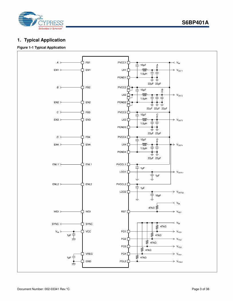
4. Preset Output Voltage
Table 4-1 Preset Output Voltage (Buck DC/DC Converter)
Channel Preset Output
Voltage [V] Soft-start Time
[ms] Maximum Output
Current [mA] Under Voltage Threshold [%]
Over Voltage Threshold [%]
DD1
1.200 1.200
2000 94.0 106.0
1.225 1.225
1.250 1.250
1.275 1.275
1.300 1.300
1.325 1.325
1.500 1.500
1.525 1.525
1.550 1.550
1.575 1.575
DD2
1.000 1.000
3000 94.0 106.0
1.025 1.025
1.050 1.050
1.075 1.075
1.100 1.100
1.125 1.125
1.150 1.150
1.175 1.175
1.200 1.200
1.225 1.225
1.250 1.250
1.275 1.275
DD3
1.200 1.200
2000 95.2 106.0
1.225 1.225
1.250 1.250
1.275 1.275
1.500 1.500
1.525 1.525
1.550 1.550
1.575 1.575
1.800 1.800
1.825 1.825
1.850 1.850
1.875 1.875
2.500 2.500
2.525 2.525
2.550 2.550
2.575 2.575
DD4
3.300 3.300
1000 95.5 106.0
3.325 3.325
3.350 3.350
3.375 3.375
3.400 3.400
Notes:
− Soft-start time values are at fOSC = 2.1 MHz
− Refer to Chapter 8 for the minimum or maximum values of output voltage, under voltage threshold and over voltage threshold.
Document Number: 002-03341 Rev.*C Page 7 of 38
S6BP401A
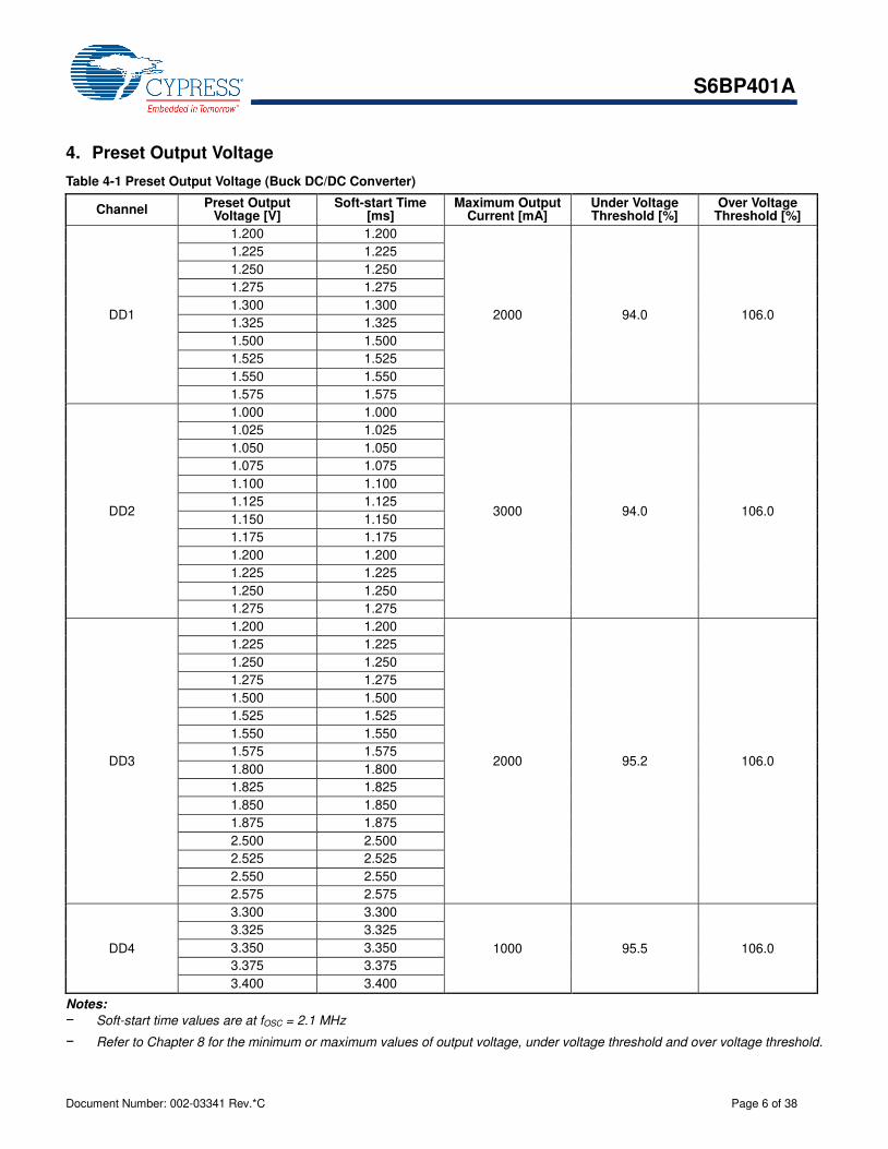
Table 4-2 Preset Output Voltage (LDO)
Channel Preset Output
Voltage [V] Soft-start Time
[ms] Maximum Output
Current [mA] Under Voltage Threshold [%]
Over Voltage Threshold [%]
LD1
3.300 3.300
200 94.0 106.0
3.325 3.325
3.350 3.350
3.375 3.375
3.400 3.400
LD2
1.200 1.200
500 94.0 106.0
1.225 1.225
1.250 1.250
1.275 1.275
1.800 1.800
1.825 1.825
1.850 1.850
1.875 1.875
2.800 2.800
2.825 2.825
2.850 2.850
2.875 2.875
Notes:
− Soft-start time values are at fOSC = 2.1 MHz
− Refer to Chapter 8 for the minimum or maximum values of output voltage, under voltage threshold and over voltage threshold.

Document Number: 002-03341 Rev.*C Page 8 of 38
S6BP401A
5. Architecture Block Diagram
Figure 5-1 Architechture Block Diagram
ErrorAmplifier
SlopeCompensation
PWMLogic
Control
PWMComparator
CurrentSense
Anti-Shoot
Through
Low Priority
en1
VoltageReference
Power GoodMonitor
Peak CurrentComparator
FB1 PVCC1
LX1
PGND1
<< DD1 >>
PGND2
PVCC2
LX2
Discharge
ss1
clk
pg1
ErrorAmplifier
SlopeCompensation
PWMLogic
Control
PWMComparator
CurrentSense
Anti-Shoot
Through
Low Priority
en2
VoltageReference
Power GoodMonitor
Peak CurrentComparator
FB2 PVCC2
LX2
PGND2
<< DD2 >>
Discharge
ss2
clk
pg2
ErrorAmplifier
SlopeCompensation
PWMLogic
Control
PWMComparator
CurrentSense
Anti-Shoot
Through
Low Priority
en3
VoltageReference
Power GoodMonitor
Peak CurrentComparator
FB3 PVCC3
LX3
PGND3
<< DD3 >>
Discharge
ss3
clk
pg3
ErrorAmplifier
SlopeCompensation
PWMLogic
Control
PWMComparator
CurrentSense
Anti-Shoot
Through
Low Priority
en4
VoltageReference
Power GoodMonitor
Peak CurrentComparator
FB4 PVCC4
LX4
PGND4
<< DD4 >>
Discharge
ss4
clk
pg4

Document Number: 002-03341 Rev.*C Page 9 of 38
S6BP401A
EN1
EN2
EN3
EN4
ENL1
ENL2
SYNC
VCC
VREG
GND
PG1
PG2
PG3
PG4
RST
ControlLogic
pg1 pg2 pg3 pg4
WatchdogTimer
pgl1
Oscillatorwith Synchronization
clk
ThermalShutdown
Under VoltageLockout
clk
en1
en2
en3
en4
enl1
enl2
Soft-StartControl
ss1
ss2
ss3
ss4
ssl1
enl2
LinearRegulator
VCC
VCC
<< Main Control >> << Power Good monitor Output >>
<< Watchdog Timer >>
WDI
clk
Power GoodMonitor
PVCCL1Low Priority
VoltageReference
Power GoodMonitor
LDO1
<< LDO1 >>
Discharge
enl1
ssl1
pgl1
PVCCL2Low Priority
VoltageReference
Power GoodMonitor
LDO2
<< LDO2 >>
Discharge
enl2
ssl2
pgl2
PGL2
pgl2

Document Number: 002-03341 Rev.*C Page 10 of 38
S6BP401A
6. Absolute Maximum Ratings
Table 6-1 Absolute Maximum Ratings
Parameter Symbol Condition Rating
Unit Min Max
Power supply voltage
VVCC VCC -0.3 +6.9 V
VPVCC PVCC1, PVCC2, PVCC3, PVCC4 -0.3 +6.9 V
VPVCCL PVCCL1, PVCCL2 -0.3 +6.9 V
Input voltage
VEN EN1, EN2, EN3, EN4, ENL1, ENL2 -0.3 +6.9 V
VWDI WDI -0.3 +6.9 V
VSYNC SYNC -0.3 +6.9 V
VFB FB1, FB2, FB3, FB4 -0.3 +6.9 V
VPG PG1, PG2, PG3, PG4, PGL2 -0.3 +6.9 V
VRST RST -0.3 +6.9 V
LX voltage VLX LX1, LX2, LX3, LX4 -0.3 +6.9 V
Voltage difference
VPVCC-VCC PVCC1 -VCC, PVCC2-VCC, PVCC3-VCC, PVCC4-VCC
-0.3 +0.3 V
VPGND-GND PGND1-GND, PGND2-GND, PGND3-GND, PGND4-GND
-0.3 +0.3 V
VPVCC-LX PVCC1-LX1, PVCC2-LX2, PVCC3-LX3, PVCC4-LX4
-0.3 +6.9 V
VVCC-INPUT
VCC-EN1, VCC-EN2, VCC-EN3, VCC-EN4, VCC-EN1L, VCC-EN2L, VCC-WDI, VCC-SYNC, VCC-FB1, VCC-FB2, VCC-FB3, VCC-FB4
-0.3 +6.9 V
Power dissipation PD TA ≤ + 25°C, Thermal resistance (θJA): 18°C /W (*1)
- 6940 mW
Junction temperature TJ - -40 +150 °C Storage temperature TSTG - -55 +150 °C
*1: When the IC is mounted on 76.2 mm × 114.3 mm four-layer epoxy board. IC is mounted on a four-layer epoxy board, which
terminal bias, and the IC’s thermal pad is connected to the epoxy board.
WARNING
1. Semiconductor devices may be permanently damaged by application of stress (including, without limitation, voltage, current or
temperature) in excess of absolute maximum ratings. Do not exceed any of these ratings.
Figure 6-1 Maximum Power Dissipation - Operating Ambient Temperature Characteristics
0
1000
2000
3000
4000
5000
6000
7000
8000
-60 -40 -20 0 20 40 60 80 100 120 140Ma
xim
um
Po
we
r d
iss
ipa
tio
nP
D
[mW
]
Ambient Temperature TA [°C]

Document Number: 002-03341 Rev.*C Page 11 of 38
S6BP401A
7. Recommended Operating Conditions
Table 7-1 Recommended Operating Conditions
Parameter Symbol Condition Value
Unit Min Typ Max
Power supply voltage
VVCC VCC +4.5 +5.0 +5.5 V
VPVCC PVCC1, PVCC2, PVCC3, PVCC4 - VVCC - V
VPVCCL PVCCL1, PVCCL2 +2.97 +5.0 VVCC V
Input voltage
VEN EN1, EN2, EN3, EN4, ENL1, ENL2 0 - VVCC V
VWDI WDI 0 - VVCC V
VSYNC SYNC 0 - VVCC V
VFB FB1, FB2, FB3, FB4 0 - VVCC V
VPG PG1, PG2, PG3, PG4, PGL2 0 - +5.5 V
VRST RST 0 - +5.5 V
Operating ambient temperature
TA - -40 +25 +125 °C
WARNING:
1. The recommended operating conditions are required in order to ensure the normal operation of the semiconductor device. All of
the device's electrical characteristics are warranted when the device is operated under these conditions.
2. Any use of semiconductor devices will be under their recommended operating condition.
3. Operation under any conditions other than these conditions may adversely affect reliability of device and could result in device
failure.
4. No warranty is made with respect to any use, operating conditions or combinations not represented on this data sheet. If you
are considering application under any conditions other than listed herein, please contact sales representatives beforehand.

Document Number: 002-03341 Rev.*C Page 12 of 38
S6BP401A
8. Electrical Characteristics
VVCC = VPVCC = 5.0V, VPVCCL = 5.0V, TA = TJ = -40 to +125 °C, unless otherwise noted. Typical values are at TA = +25 °C.
Table 8-1 Electrical Characteristics
Parameter Symbol Condition Value
Unit Min Typ Max
Supply Current
Shutdown current IVCCS VCC PIN, VEN1 = VEN2 = VEN3 = VEN4 = VENL1 = VENL2 = 0V
- 1 10 µA
UVLO: Under Voltage Lockout (VCC)
Threshold voltage VUVLOF VVCC falling, UVLO stop voltage 3.80 3.95 4.10 V
Hysteresis VUVHYS - 0.27 0.30 0.33 V
TSD: Thermal Shutdown
Shutdown temperature TTSD Temperature rising - 165 (*1) - °C
Hysteresis TTSDHYS - - 10 (*1) - °C
Enable Inputs (EN1, EN2, EN3, EN4, ENL1, ENL2)
Input high voltage VIHEN - 2.0 - VVCC V
Input low voltage VILEN - 0 - 0.4 V
Input current IIHEN VEN = 5.0V 33 50 100 µA
Pull down resistance RPDEN - 50 100 150 kΩ
Internal Linear Regulator Output (VREG)
Output voltage VVREG VVCC = 5.0V 1.74 1.80 1.86 V Maximum output current
IVREG VVCC = 5.0V 5 - - mA
Over voltage lockout threshold
VVREGOVR VVREG rising, Power fail 1.86 1.92 1.98 V VVREGOVF VVREG falling, Power good 1.81 1.87 1.93 V
Under voltage lockout threshold
VVREGUVR VVREG rising, Power good 1.67 1.73 1.79 V VVREGUVF VVREG falling, Power fail 1.62 1.68 1.74 V
Oscillator
Switching frequency fOSC - 2.0 2.1 2.2 MHz
Synchronization Input (SYNC)
Input high voltage VIHSYNC - 2.0 - VVCC V Input Low voltage VILSYNC - 0 - 0.4 V Input current IIHSYNC VEN = 5.0V 33 50 100 µA Pull down resistance RPDSYNC - 50 100 150 kΩ Input frequency fSYNC - 1.8 2.1 2.4 MHz Switching frequency fOSC - - fSYNC - MHz

Document Number: 002-03341 Rev.*C Page 13 of 38
S6BP401A
Parameter Symbol Condition Value
Unit Min Typ Max
Power Good Monitor (PG1, PG2, PGL2)
Over voltage threshold
VPGOV Ratio of power fail threshold to VOUT1, VOUT2, VOUTL2 rising
104.5 106.0 107.5 %
Over voltage hysteresis
VPGOVHYS - 0.5 1.0 1.5 %
Under voltage threshold
VPGUV Ratio of power fail threshold to VOUT1, VOUT2, VOUT3 falling
92.5 94.0 95.5 %
Under voltage hysteresis
VPGUVHYS - 0.5 1.0 1.5 %
Leakage current ILEAKPG VPG = 5.0V - - 1 µA Output low voltage VOLPG IPG = 3 mA - 0.15 0.30 V Propagation time TPPG 5% outside of the threshold, Power fail - 4 (*1) 8 (*1) µs Power-on reset time TRPG Power good 8 10 12 ms
Power Good Monitor (PG3)
Over voltage threshold
VPGOV Ratio of power fail threshold to VOUT3 rising 104.5 106.0 107.5 %
Over voltage hysteresis
VPGOVHYS - 0.5 1.0 1.5 %
Under voltage threshold
VPGUV Ratio of power fail threshold to VOUT3 falling 93.7 95.2 96.7 %
Under voltage hysteresis
VPGUVHYS - 0.5 1.0 1.5 %
Leakage current ILEAKPG VPG = 5.0V - - 1 µA Output low voltage VOLPG IPG = 3 mA - 0.15 0.30 V Propagation time TPPG 5% outside of the threshold, Power fail - 4 (*1) 8 (*1) µs Power-on reset time TRPG Power good 8 10 12 ms
Power Good Monitor (PG4)
Over voltage threshold
VPGOV Ratio of power fail threshold to VOUT4 rising 104.5 106.0 107.5 %
Over voltage hysteresis
VPGOVHYS - 0.5 1.0 1.5 %
Under voltage threshold
VPGUV Ratio of power fail threshold to VOUT4 falling 94.0 95.5 97.0 %
Under voltage hysteresis
VPGUVHYS - 0.5 1.0 1.5 %
Leakage current ILEAKPG VPG = 5.0V - - 1 µA Output low voltage VOLPG IPG = 3 mA - 0.15 0.30 V Propagation time TPPG 5% outside of the threshold, Power fail - 4 (*1) 8 (*1) µs Power-on reset time TRPG Power good 8 10 12 ms
Reset (RST)
Over voltage threshold
VRSOV Ratio of power fail threshold to VOUTL1 rising 104.5 106.0 107.5 %
Over voltage hysteresis
VRSOVHYS - 0.5 1.0 1.5 %
Under voltage threshold
VRSUV Ratio of power fail threshold to VOUTL1 falling 92.5 94.0 95.5 %
Under voltage hysteresis
VRSUVHYS - 0.5 1.0 1.5 %
Leakage current ILEAKRST VRST = 5.0V - - 1 µA Output low voltage VOLRST IPG = 3 mA - 0.15 0.30 V Propagation time TPRST 5% outside of the threshold, Power fail - 4 (*1) 8 (*1) µs Power-on reset time TRD Power good 25.6 32.0 38.4 ms

Document Number: 002-03341 Rev.*C Page 14 of 38
S6BP401A
Parameter Symbol Condition Value
Unit Min Typ Max
Watchdog Timer (WDI)
Watchdog sampling time
TSAM - 0.40 0.50 0.60 ms
Ignore window time TIW - 25.6 32.0 38.4 ms Open window time TOW - 25.6 32.0 38.4 ms Long open window time
TLOW - 102.4 128.0 153.6 ms
Closed window time TCW - 25.6 32.0 38.4 ms Window watchdog trigger time
TWD - 38.4 48 51.2 ms
Input high voltage VIHWDI - 2.0 - VVCC V Input low voltage VILWDI - 0 - 0.4 V Input current IIHWDI VWDI = 5.0V 33 50 100 µA Pull down resistance RPDWDI - 50 100 150 kΩ
DD1: Buck DC/DC Converter
Output voltage accuracy
VOUT1 VVCC = 5.0V, IOUT1 = 10 mA
-1.8 0 +1.8 %
DC regulation VREG1 VVCC = VPVCC1 = 4.5 to 5.5V, IOUT1 = 0 to 2.0A
-15 (*1) 0 +5 (*1) mV
FB1 input resistance RFB1 VFB1 = 2.0V 95 190 285 kΩ
Switching FET ON resistance
RONHS1 ILX1 = 20 mA (PVCC1 to LX1) - 100 190 mΩ RONLS1 ILX1 = -20 mA (LX1 to PGND1) - 65 125 mΩ
Switching FET leakage current
ILEAK1 IPVCC1 = 5.0V - 1 10 µA
Maximum output current
IOUT1 L = 1.5 µH 2 (*1) - - A
LX1 peak current limit ILIMIT1 L = 1.5 µH 2.5 (*1) - - A
Over voltage protection threshold
VOVP1 VOUT1 rising, Switching termination threshold
125.0 130.0 135.0 %
Over voltage protection hysteresis
VOVPHYS1 - 2.0 5.0 8.0 %
FB1 discharge resistance
RDIS1 - 160 400 640 Ω
Soft-start time coefficient
TCOESS1 TSS1 = VOUT1 x TCOESS1 0.9 1.0 1.1 ms/V
DD2: Buck DC/DC Converter
Output voltage accuracy
VOUT2 VVCC = 5.0V, IOUT2 = 10 mA
-1.8 0 +1.8 %
DC regulation VREG2 VVCC = VPVCC2 = 4.5 to 5.5V IOUT2 = 0 to 3.0A
-15 (*1) 0 +5 (*1) mV
FB2 input resistance RFB2 VFB2 = 2.0V 95 190 285 kΩ
Switching FET ON resistance
RONHS2 ILX2 = 20 mA (PVCC2 to LX2) - 85 165 mΩ
RONLS2 ILX2 = -20 mA (LX2 to PGND2) - 55 105 mΩ Switching FET leakage current
ILEAK2 IPVCC2 = 5.0V - 1 10 µA
Maximum output current
IOUT2 L = 1.5 µH 3 (*1) - - A
LX2 peak current limit ILIMIT2 L = 1.5 µH 3.5 (*1) - - A Over voltage protection threshold
VOVP2 VOUT2 rising, Switching termination threshold
125.0 130.0 135.0 %
Over voltage protection hysteresis
VOVPHYS2 - 2.0 5.0 8.0 %
FB2 discharge resistance
RDIS2 - 160 400 640 Ω
Soft-start time coefficient
TCOESS2 TSS2 = VOUT2 x TCOESS2 0.9 1.0 1.1 ms/V

Document Number: 002-03341 Rev.*C Page 15 of 38
S6BP401A
Parameter Symbol Condition Value
Unit Min Typ Max
DD3: Buck DC/DC Converter
Output voltage accuracy
VOUT3 VVCC = 5.0V, IOUT3 = 10 mA
-1.8 0 +1.8 %
DC regulation VREG3 VVCC = VPVCC3 = 4.5 to 5.5V, IOUT3 = 0 to 2.0A
-15 (*1) 0 +5 (*1) mV
FB3 input resistance RFB3 VFB3 = 2.0V 95 190 285 kΩ
Switching FET ON resistance
RONHS3 ILX3 = 20 mA (PVCC3 to LX3) - 100 190 mΩ RONLS3 ILX3 = -20 mA (LX3 to PGND3) - 65 125 mΩ
Switching FET leakage current
ILEAK3 IPVCC3 = 5.0V - 1 10 µA
Maximum output current
IOUT3 L = 1.5 µH 2 (*1) - - A
LX3 peak current limit ILIMIT3 L = 1.5 µH 2.5 (*1) - - A
Over voltage protection threshold
VOVP3 VOUT3 rising, Switching termination threshold
125.0 130.0 135.0 %
Over voltage protection hysteresis
VOVPHYS3 - 2.0 5.0 8.0 %
FB3 discharge resistance
RDIS3 - 160 400 640 Ω
Soft-start time coefficient
TCOESS3 TSS3 = VOUT3 × TCOESS3 0.9 1.0 1.1 ms/V
DD4: Buck DC/DC Converter
Output voltage accuracy
VOUT4 VVCC = 5.0V, IOUT4 = 10 mA
-1.8 0 +1.8 %
DC regulation VREG4 VVCC = VPVCC4 = 4.5 to 5.5V, IOUT4 = 0 to 1.0A
-15 (*1) 0 +5 (*1) mV
FB4 input resistance RFB4 VFB4 = 2.0V 95 190 285 kΩ
Switching FET ON resistance
RONHS4 ILX4 = 20 mA (PVCC4 to LX4) - 100 190 mΩ
RONLS4 ILX4 = -20 mA (LX4 to PGND4) - 65 125 mΩ Switching FET leakage current
ILEAK4 IPVCC4 = 5.0V - 1 10 µA
Maximum output current
IOUT4 L = 1.5 µH 1 (*1) - - A
LX4 peak current limit ILIMIT4 L = 1.5 µH 1.5 (*1) - - A Over voltage protection threshold
VOVP4 VOUT4 rising, Switching termination threshold
125.0 130.0 135.0 %
Over voltage protection hysteresis
VOVPHYS4 - 2.0 5.0 8.0 %
FB4 discharge resistance
RDIS4 - 160 400 640 Ω
Soft-start time coefficient
TCOESS4 TSS4 = VOUT4 × TCOESS4 0.9 1.0 1.1 ms/V

Document Number: 002-03341 Rev.*C Page 16 of 38
S6BP401A
Parameter Symbol Condition Value
Unit Min Typ Max
LD1: LDO Regulator
Output voltage accuracy
VOUTL1 VVCC = 5.0V, IOUTL1 = 10 mA
-1.8 0 +1.8 %
DC regulation VREGL1 VVCC = 4.5 to 5.5V, VPVCCL1 = 2.97 to VVCC IOUTL1 = 0 to IOUTL1
-15 (*1) 0 +5 (*1) mV
Output FET leakage current
ILEAKL1 IPVCCL1=5.0V - 1 10 µA
Maximum output current
IOUTL1 VPVCCL1 - VOUTL1 ≥ 1.6V 200 (*1) - - mA
0.17V ≤ VPVCCL1 - VOUTL1 < 1.6V 100 (*1) - - mA
Output current limit ILIMITL1 VPVCCL1 - VOUTL1 ≥ 1.6V 210 (*1) - - mA 0.17V ≤ VPVCCL1 - VOUTL1 < 1.6V 105 (*1) - - mA
LDO1 discharge resistance
RDISL1 - 160 400 640 Ω
Soft-start time coefficient
TCOESSL1 TSSL1 = VOUTL1 × TCOESSL1 0.9 1.0 1.1 ms/V
LD2: LDO Regulator
Output voltage accuracy
VOUTL2 VVCC = 5.0V, IOUTL2 = 10 mA
-1.8 0 +1.8 %
DC regulation VREGL2 VVCC = 4.5 to 5.5V, VPVCCL2 = 2.97 to VVCC IOUTL2 = 0 to IOUTL2
-15 (*1) 0 +5 (*1) mV
Output FET leakage current
ILEAKL2 IPVCCL2=5.0V - 1 10 µA
Maximum output current
IOUTL2 VPVCCL2 - VOUTL2 ≥ 1.6V 500 (*1) - - mA 0.17V ≤ VPVCCL2 - VOUTL2 < 1.6V 400 (*1) - - mA
Output current limit ILIMITL2 VPVCCL2 - VOUTL2 ≥ 1.6V 525 (*1) - - mA 0.17V ≤ VPVCCL2 - VOUTL2 < 1.6V 420 (*1) - - mA
LDO2 discharge resistance
RDISL2 - 160 400 640 Ω
Soft-start time coefficient
TCOESSL2 TSSL2 = VOUTL2 × TCOESSL2 0.9 1.0 1.1 ms/V
*1: The electrical characteristic is ensured by statistical characterization and indirect tests.

Document Number: 002-03341 Rev.*C Page 17 of 38
S6BP401A
9. Operating Mode List
Table 9-1 shows the operation list of S6BP401A.
Table 9-1 Operation Mode List
Condition Operating Block
TJ SYNC ENL1
EN1/ EN2/ EN3/ EN4/ ENL2
Chip Control
VREG LDO Watch-
dog Trigger Monitor
Freq. Sync.
LD1
DD1/ DD2/ DD3/ DD4/ LD2
< TTSD L or H L L OFF OFF OFF OFF OFF OFF
< TTSD L or H L H ON ON OFF OFF OFF ON
< TTSD L or H H L ON ON ON OFF ON OFF
< TTSD L or H H H ON ON ON OFF ON ON
< TTSD clock L L OFF OFF OFF OFF OFF OFF
< TTSD clock L H ON ON OFF ON OFF ON
< TTSD clock H L ON ON ON ON ON OFF
< TTSD clock H H ON ON ON ON ON ON
≥ TTSD L or H L L OFF OFF OFF OFF OFF OFF
≥ TTSD L or H L H ON ON OFF OFF OFF OFF
≥ TTSD L or H H L ON ON OFF OFF OFF OFF
≥ TTSD L or H H H ON ON OFF OFF OFF OFF
≥ TTSD clock L L OFF OFF OFF OFF OFF OFF
≥ TTSD clock L H ON ON OFF OFF OFF OFF
≥ TTSD clock H L ON ON OFF OFF OFF OFF
≥ TTSD clock H H ON ON OFF OFF OFF OFF

Document Number: 002-03341 Rev.*C Page 18 of 38
S6BP401A
10. Function
10.1 Turning ON and OFF Sequence
When all of the enable input terminals (EN1, EN2, EN3, EN4, ENL1 and ENL2) are “Low”, the device is in shutdown state. When any one or more than one of them go “High,” the device is initialized, then the internal linear regulator (VREG) starts generating 1.8V
internal supply voltage. After that, each DC/DC converters and LDOs state is transitioned to the state which can be started.
In order for the device to start, the VCC terminal voltage must be higher than the under-voltage lockout threshold (VUVLOF + VUVHYS).
Figure 10-1 depicts the turning-on and off sequence where the enable signals are connected to VCC. Figure 10-2 depicts that where
the enable signals are respectively controlled after the IC is powered.
Figure 10-1 Turning ON and OFF Sequence (where EN1 and ENL1 are Connected to VCC)
*1: Given that the system employs the same external parts with those specified in “11. Application Circuit Example”.
Time
VRST
VVREG
VOUTL1
VOUT1 VPGUV+VPGUVHYS
VENL1
VEN1
VVCC
VRSUV+VRSUVHYS
Initialization(TYP:1ms)
TRD
VUVLOF
TYP:40.5ms(*1)
10%
10%
TYP:0.92ms(*1)
VUVLOF + VUVHYS

Document Number: 002-03341 Rev.*C Page 19 of 38
S6BP401A
Figure 10-2 Turning ON and OFF Sequence (where EN1 and ENL1 are Respectively Controlled)
*1: Given that the system employs the same external parts with those specified in “11. Application Circuit Example”.
Time
VRST
VVREG
VOUTL1
VOUT1 VPGUV+VPGUVHYS
VENL1
VEN1
VVCC
VRSUV+VRSUVHYS
Initialization(TYP:1ms)
TRD Initialization(TYP:1ms)
10%
10%
TYP:40.5ms(*1)
TYP:0.92ms(*1)
VUVLOF + VUVHYS

Document Number: 002-03341 Rev.*C Page 20 of 38
S6BP401A
10.2 Over Current Protection
The over current protection of the DC/DC converters detects the inductor peak current with on-resistance of Internal high side
switching FET. If the DC/DC converter is over current state, the corresponding output voltage is decreased. If the device returns
from over current state, the output voltage is target voltage.
Each LDOs equips foldback current limiter in order to prevent the IC itself from being damaged or destroyed. The curve of output
current and output voltage in over current state is shown in the Figure 10-3.
Figure 10-3 LDO Foldback Over Current Protection Characteristic
10.3 Over Voltage Protection The over voltage protection of the DC/DC converters detects the output voltage. If the DC/DC converter is over voltage state, the
corresponding channel stops switching and inductor connecting terminal (LX1, LX2, LX3, LX4) is held at high impedance. If the
device returns from over voltage state, the channel returns switching automatically.
Figure 10-4 Over Voltage Protection Timing Chart
Current
Voltage
IOUTL1
IOUTL2
ILIMITL1
ILIMITL2
VOUTL1
VOUTL2
ISL1
ISL2
Time
VPG1,VPG2,VPG3,VPG4
TRPGTPPG
VEN1,VEN2,VEN3,VEN4
VOUT1,VOUT2,VOUT3,VOUT4
TRPG
VPGOVHYS
VPGOV
Hi-Z
ON
LX1, LX2,LX3, LX4
Discharge OFF
Switching Hi-Z Switching
VOVP1, VOVP2,VOVP3, VOVP4
VOVPHYS1, VOVPHYS2,VOVPHYS3, VOVPHYS4

Document Number: 002-03341 Rev.*C Page 21 of 38
S6BP401A
10.4 Thermal Shutdown (TSD)
If the junction temperature reaches +165°C, all DC/DC converters and LDOs stop outputting voltage. Then the discharge operation
is carried out to discharge the output capacitor (The discharge operation continues until the state of the thermal shutdown released.)
When the junction temperature drops below +155°C, the soft-starters activate regulators and start generating voltage gradually if the
enable is "High."
Figure 10-5 Thermal Shutdown Timing Chart
10.5 Under Voltage Lockout (UVLO) If the VCC terminal voltage (VVCC) drops below the lower UVLO threshold (VUVLOF), all DC/DC converters (DD1, DD2, DD3, DD4),
LDOs (LD1, LD2), windowed watchdog timer (WDT) and the internal linear regulator (VREG) stop working. When the VCC terminal
voltage (VVCC) is raised higher than the higher UVLO threshold (VUVLOF + VUVHYS), the device returns automatically.
10.6 Soft-Start Operation
S6BP401A equips load-independent soft-start function in order to prevent the DC/DC converters and LDOs from having rush current
at the start-up. The soft-start timing is shown in the Figure 10-6, and is given by the following equation;
𝑇𝑆𝑆 = 𝑉𝑂𝑈𝑇 × 𝑇𝐶𝑂𝐸𝑆𝑆, where
TSS [ms] : Soft-start time
VOUT [V] : Output voltage (VOUT1, VOUT2, VOUT3, VOUT4, VOUTL1, VOUTL2)
TCOESS [ms/V] : Soft-start time coefficient (TCOESS1, TCOESS2, TCOESS3, TCOESS4, TCOESSL1, TCOESSL2)
165 deg.155 deg.
TJ
VEN1
VOUT1
Time
Soft-Start Soft-Start

Document Number: 002-03341 Rev.*C Page 22 of 38
S6BP401A
Figure 10-6 Soft-Start Operation Timing Chart
10.7 Discharge Operation
When an enable signal goes “Low”, the corresponding output capacitor is discharged by the internal discharge resistor and the
output voltage is decreased gradually. Note that the discharge time is not consistent: it depends on the output load current.
As for a DC/DC converter, the output capacitor is discharged from FB1, FB2, FB3 and FB4 terminal to PGND1, PGND2, PGND3
and PGND4 terminal respectively. As for a LDO, the output capacitor is dis-charged from LDO1, LDO2 terminal to GND terminal.
The discharge time required to decrease the output voltage by 90% without any explicit load given by the following equation; 𝑇𝐷𝐼𝑆 = 2.3 × 𝑅𝐷𝐼𝑆 × 𝐶𝑂𝑈𝑇, where
TDIS [ms] : Discharge time
RDIS [kΩ] : Discharge resistance (RDIS1, RDIS2, RDIS3, RDIS4, RDISL1, RDISL2)
COUT [µF] : Output capacitor
Figure 10-7 Discharge Diagram (DC/DC Converter)
enable
Error Amp.
PWMControl
PowerSupply
PVCC1,PVCC2,PVCC3,PVCC4
LX1,LX2,LX3,LX4
PGND1,PGND2,PGND3,PGND4
FB1,FB2,FB3,FB4
RDIS1,RDIS2,RDIS3,RDIS4
VEN
VOUT
Time
TSS=VOUT(1)×TCOESS
VOUT(1)
VOUT(2)
VOUT(3)
TSS=VOUT(2)×TCOESS
TSS=VOUT(3)×TCOESS

Document Number: 002-03341 Rev.*C Page 23 of 38
S6BP401A
Figure 10-8 Discharge Diagram (LDO)
10.8 Power Good Monitor and Reset Function Each DC/DC converters and LDOs has power good function to indicate whether the output voltage is in the expected range. The
Table 10-1 describes the power good pin names and their functions of each DC/DC converters and LDOs. The Figure 10-9 and
Figure 10-10 depict power-good timing chart.
Table 10-1 Power Good Monitor and Reset Function Pin List
Channel Pin Name Description
DD1 PG1
Enabling DD1 is followed by rising of the DD1 output voltage (VOUT1). Once VOUT1 reaches within the power good range (VPGUV + VPGUVHYS < VOUT1 < VPGOV – VPGOVHYS), the power good monitor output (PG1 terminal) changes its state from “Low” to “Open” after a power-on-reset time (TRPG). When VOUT1 is out of the power good range (VOUT1 ≤ VPGUV or VOUT1 ≥ VPGOV), PG1 terminal changes its state from “Open” to “Low” after the propagation delay (TPPG). The glitch within TPPG does not affect the power good monitor output.
DD2 PG2
Enabling DD2 is followed by rising of the DD2 output voltage (VOUT2). Once VOUT2 reaches within the power good range (VPGUV + VPGUVHYS < VOUT2 < VPGOV – VPGOVHYS), the power good monitor output (PG2 terminal) changes its state from “Low” to “Open” after a power-on-reset time (TRPG). When VOUT2 is out of the power good range (VOUT2 ≤ VPGUV or VOUT2 ≥ VPGOV), PG2 terminal changes its state from “Open” to “Low” after the propagation delay (TPPG). The glitch within TPPG does not affect the power good monitor output.
DD3 PG3
Enabling DD3 is followed by rising of the DD3 output voltage (VOUT3). Once VOUT3 reaches within the power good range (VPGUV + VPGUVHYS < VOUT3 < VPGOV – VPGOVHYS), the power good monitor output (PG3 terminal) changes its state from “Low” to “Open” after a power-on-reset time (TRPG). When VOUT3 is out of the power good range (VOUT3 ≤ VPGUV or VOUT3 ≥ VPGOV), PG3 terminal changes its state from “Open” to “Low” after the propagation delay (TPPG). The glitch within TPPG does not affect the power good monitor output.
DD4 PG4
Enabling DD4 is followed by rising of the DD4 output voltage (VOUT4). Once VOUT4 reaches within the power good range (VPGUV + VPGUVHYS < VOUT4 < VPGOV – VPGOVHYS), the power good monitor output (PG4 terminal) changes its state from “Low” to “Open” after a power-on-reset time (TRPG). When VOUT4 is out of the power good range (VOUT4 ≤ VPGUV or VOUT4 ≥ VPGOV), PG4 terminal changes its state from “Open” to “Low” after the propagation delay (TPPG). The glitch within TPPG does not affect the power good monitor output.
enable
PowerSupply
PVCCL1,PVCCL2
LDO1,LDO2
RDISL1,RDISL2

Document Number: 002-03341 Rev.*C Page 24 of 38
S6BP401A
Channel Pin Name Description
LD1 RST
Enabling LD1 is followed by rising of the LD1 output voltage (VOUTL1). Once VOUTL1 reaches within the power good range (VRSUV + VRSUVHYS < VOUTL1 < VRSOV - VRSOVHYS), the RST terminal changes its state from “Low” to “Open” after a power-on-reset time (TRD). When VOUTL1 is out of the power good range (VOUTL1 ≤ VRSUV or VOUTL1 ≥ VRSOV), RST terminal changes “Open” to “Low” after the propagation delay (TPRST). The glitch within TPRST does not affect the power good monitor output.
LD2 PGL2
Enabling LD2 is followed by rising of the LD2 output voltage (VOUTL2). Once VOUTL2 reaches within the power good range (VPGUV + VPGUVHYS < VOUTL2 < VPGOV – VPGOVHYS), the power good monitor output (PGL2 terminal) changes its state from “Low” to “Open” through the power-on-reset time (TRPG). When VOUTL2 is out of the power good range (VOUTL2 ≤ VPGUV or VOUTL2 ≥ VPGOV), PGL2 terminal changes “Open” to “Low” after the propagation delay (TPPG). The glitch within TPPG does not affect the power good monitor output.
Figure 10-9 Power-Good Monitor Output Timing Chart (PG1, PG2, PG3, PG4, PGL2)
Figure 10-10 Power-Good Monitor Output Timing Chart (RST)
Time
VPG1,VPG2,VPG3,VPG4,VPGL2
TRPG < TPPG TPPG
VEN1,VEN2,VEN3,VEN4,VENL2
VOUT1,VOUT2,VOUT3,VOUT4,VOUTL2
< TPPG
Not reset
TRPG
VPGOVHYS
VPGUVHYS
VPGOV
VPGUV
TPPG TRPG
Time
VRST
TRD < TPRST TPRST
VENL1
VOUTL1
< TPRST
Not reset
TRD
VRSOVHYS
VRSUVHYS
VRSOV
VRSUV
TPRST TRD
Document Number: 002-03341 Rev.*C Page 25 of 38
S6BP401A
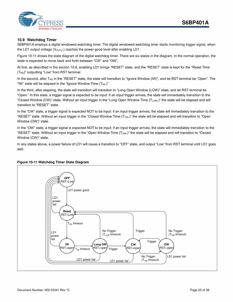
10.9 Watchdog Timer
S6BP401A employs a digital windowed watchdog timer. The digital windowed watchdog timer starts monitoring trigger signal, when
the LD1 output voltage (VOUTL1) reaches the power good level after enabling LD1.
Figure 10-11 shows the state diagram of the digital watchdog timer. There are six states in the diagram. In the normal operation, the
state is expected to move back and forth between “CW” and “OW”,
At first, as described in the section 10.8, enabling LD1 brings “RESET” state, and the “RESET” state is kept for the “Reset Time (TRD)” outputting “Low” from RST terminal.
In the second, after TRD in the “RESET” state, the state will transition to “Ignore Window (IW)”, and let RST terminal be “Open”. The “IW” state will be elapsed in the “Ignore Window Time (TIW.)”
In the third, after elapsing, the state will transition will transition to “Long Open Window (LOW)” state, and let RST terminal be
“Open.” In this state, a trigger signal is expected to be input: if an input trigger arrives, the state will immediately transition to the
“Closed Window (CW)” state. Without an input trigger in the “Long Open Window Time (TLOW,)” the state will be elapsed and will
transition to “RESET” state.
In the “CW” state, a trigger signal is expected NOT to be input: if an input trigger arrives, the state will immediately transition to the
“RESET” state. Without an input trigger in the “Closed Window Time (TCW,)” the state will be elapsed and will transition to “Open Window (OW)” state.
In the “OW” state, a trigger signal is expected NOT to be input: if an input trigger arrives, the state will immediately transition to the
“RESET” state. Without an input trigger in the “Open Window Time (TOW,)” the state will be elapsed and will transition to “Closed Window (CW)” state.
In any states above, a power failure of LD1 will cause a transition to “OFF” state, and output “Low” from RST terminal until LD1 goes
well.
Figure 10-11 Watchdog Timer State Diagram
OFFRST=Low
ResetRST=Low
IWRST=open
Long OWRST=open
OWRST=open
CWRST=open
LD1 power failLD1 power fail
LD1powerfail
Trigger
LD1 power fail
No Trigger(TOW timeout)
Trigger
No Trigger(TCW timeout)
LD1 power good
TRD timeout
TIW timeout Trigger
No Trigger(TLOW timeout)
LD1powerfail