Embed Size (px)
Citation preview

S1D13506 LCD/CRT/TV Controller
S5U13506P00C100 PCI Evaluation Board User Manual
Document Number: X25B-G-014-02
Status: Revision 2.0
Issue Date: 2009/03/02
© SEIKO EPSON CORPORATION 2006 - 2009. All Rights Reserved.
Information in this document is subject to change without notice. You may download and use this document, but only for your own use inevaluating Seiko Epson/EPSON products. You may not modify the document. Epson Research and Development, Inc. disclaims anyrepresentation that the contents of this document are accurate or current. The Programs/Technologies described in this document may contain material protected under U.S. and/or International Patent laws.
EPSON is a registered trademark of Seiko Epson Corporation. All other Trademarks are the property of their respective owners.

Page 2 Epson Research and DevelopmentVancouver Design Center
S1D13506 S5U13506P00C100 PCI Evaluation Board User ManualX25B-G-014-02 Issue Date: 2009/03/02
THIS PAGE LEFT BLANK

Epson Research and Development Page 3Vancouver Design Center
S5U13506P00C100 PCI Evaluation Board User Manual S1D13506Issue Date: 2009/03/02 X25B-G-014-02
Table of Contents
1 Introduction . . . . . . . . . . . . . . . . . . . . . . . . . . . . . . . . . . . . . . . . 5
2 Features . . . . . . . . . . . . . . . . . . . . . . . . . . . . . . . . . . . . . . . . . . 6
3 Installation and Configuration . . . . . . . . . . . . . . . . . . . . . . . . . . . . . . 73.1 Configuration DIP Switches . . . . . . . . . . . . . . . . . . . . . . . . . . 7
3.2 Configuration Jumpers . . . . . . . . . . . . . . . . . . . . . . . . . . . . 9
4 Technical Description . . . . . . . . . . . . . . . . . . . . . . . . . . . . . . . . . 144.1 PCI Bus Support . . . . . . . . . . . . . . . . . . . . . . . . . . . . . 14
4.2 Non-PCI Host Interface Support . . . . . . . . . . . . . . . . . . . . . . . 14
4.2.1 CPU Interface Pin Mapping . . . . . . . . . . . . . . . . . . . . . . . . . . . . . . 15
4.2.2 CPU Bus Connector Pin Mapping . . . . . . . . . . . . . . . . . . . . . . . . . . 16
4.3 LCD Support . . . . . . . . . . . . . . . . . . . . . . . . . . . . . . . 18
4.3.1 LCD Interface Pin Mapping . . . . . . . . . . . . . . . . . . . . . . . . . . . . . . 19
4.3.2 Buffered LCD Connector . . . . . . . . . . . . . . . . . . . . . . . . . . . . . . . 20
4.4 CRT/TV Support . . . . . . . . . . . . . . . . . . . . . . . . . . . . . 21
4.4.1 CRT/TV Interface Pin Mapping . . . . . . . . . . . . . . . . . . . . . . . . . . . . 21
4.4.2 CRT Support . . . . . . . . . . . . . . . . . . . . . . . . . . . . . . . . . . . . . 21
4.4.3 TV Support . . . . . . . . . . . . . . . . . . . . . . . . . . . . . . . . . . . . . . 21
4.5 Current consumption measurement . . . . . . . . . . . . . . . . . . . . . . 21
5 References . . . . . . . . . . . . . . . . . . . . . . . . . . . . . . . . . . . . . . . 225.1 Documents . . . . . . . . . . . . . . . . . . . . . . . . . . . . . . . 22
5.2 Document Sources . . . . . . . . . . . . . . . . . . . . . . . . . . . . 22
6 Parts List . . . . . . . . . . . . . . . . . . . . . . . . . . . . . . . . . . . . . . . . 23
7 Schematic Diagrams . . . . . . . . . . . . . . . . . . . . . . . . . . . . . . . . . . 25
8 Board Layout . . . . . . . . . . . . . . . . . . . . . . . . . . . . . . . . . . . . . . 30
9 Technical Support . . . . . . . . . . . . . . . . . . . . . . . . . . . . . . . . . . . 319.1 EPSON LCD/CRT Controllers (S1D13506) . . . . . . . . . . . . . . . . . . 31

Page 4 Epson Research and DevelopmentVancouver Design Center
S1D13506 S5U13506P00C100 PCI Evaluation Board User ManualX25B-G-014-02 Issue Date: 2009/03/02
THIS PAGE LEFT BLANK

Epson Research and Development Page 5Vancouver Design Center
S5U13506P00C100 PCI Evaluation Board User Manual S1D13506Issue Date: 2009/03/02 X25B-G-014-02
1 Introduction
This manual describes the setup and operation of the S5U13505P00C100 PCI Evaluation Board. The S5U13506P00C100 is designed as an evaluation platform for the S1D13506 Color LCD/CRT/TV Controller chip.
This document is updated as appropriate. Please check the Epson Research and Devel-opment website at http://www.erd.epson.com for the latest revision of this document before beginning any development.
We appreciate your comments on our documentation. Please contact us via email at [email protected].

Page 6 Epson Research and DevelopmentVancouver Design Center
S1D13506 S5U13506P00C100 PCI Evaluation Board User ManualX25B-G-014-02 Issue Date: 2009/03/02
2 Features
The S5U13506P00C100 features the following:
• S1D13506 Color LCD/CRT/TV controller chip
• PCI bus operation using on-board PCI bridge
• Headers for connecting to a 3.3V host bus interface (5V host bus interface also possible with modifications to the board)
• 1Mx16 EDO DRAM
• Configuration options
• Headers for S1D13506 current consumption measurements
• 4/8-bit 3.3V or 5V monochrome passive LCD panel support
• 4/8/16-bit 3.3V or 5V color passive LCD panel support
• 9/12/18-bit 3.3V or 5V TFT/D-TFD LCD panel support
• Embedded RAMDAC for CRT and TV support
• Software initiated Power Save Mode

Epson Research and Development Page 7Vancouver Design Center
S5U13506P00C100 PCI Evaluation Board User Manual S1D13506Issue Date: 2009/03/02 X25B-G-014-02
3 Installation and Configuration
The S5U13506P00C100 is designed to support as many platforms as possible. The board incorporates a DIP switch and several jumpers which allow both evaluation board and S1D13506 LCD controller settings to be configured for a specified evaluation platform.
3.1 Configuration DIP Switches
The S1D13506 LCD controller has 16 configuration inputs (MD[15:0]) which are read on the rising edge of RESET#. Where appropriate, the S5U13506P00C100 hard-wires some of these configuration inputs, but in order to configure the S1D13505 for multiple host bus interfaces an eight-position DIP switch is required. The following figure shows the location of DIP switch S1 on the S5U13506P00C100 board.
Figure 3-1: Configuration DIP Switch (S1) Location
DIP Switch - S1

Page 8 Epson Research and DevelopmentVancouver Design Center
S1D13506 S5U13506P00C100 PCI Evaluation Board User ManualX25B-G-014-02 Issue Date: 2009/03/02
The following DIP switch settings configure the S1D13506.
The following table shows the Host Bus Interface options available. The host bus interface is selected according to the evaluation platform to be used.
Table 3-1: Configuration DIP Switch Settings
Switch SignalValue of this pin at rising edge of RESET# is used to configure:
Closed/On=1 Open/Off=0
S1-1 MD15 WAIT# is always driven. WAIT# is tristated when S1D13506 is not selected
S1-2 MD1
See Table 3-2:, “Host Bus Interface Selection” on page 8S1-3 MD2
S1-4 MD3
S1-5 MD4 Little Endian Big Endian
S1-6 MD5 WAIT# is active high WAIT# is active low
S1-7 MD11 See Table 3-2:, “Host Bus Interface Selection” on page 8
S1-8 MD12 BUSCLK input divided by 2 BUSCLK input not divided
= Required configuration when used in a PCI environment
Table 3-2: Host Bus Interface Selection
MD11 MD3 MD2 MD1 Host Bus Interface
0 0 0 0 SH-4/SH-3
0 0 0 1 MC68K Bus 1
0 0 1 0 MC68K Bus 2
0 0 1 1 Generic
0 1 0 0 Reserved
0 1 0 1 MIPS/ISA
0 1 1 0 PowerPC
0 1 1 1 PC Card
1 1 1 1 Philips PR31500/PR31700 / Toshiba TX3912
= Required configuration when used in a PCI environment
Epson Research and Development Page 9Vancouver Design Center
S5U13506P00C100 PCI Evaluation Board User Manual S1D13506Issue Date: 2009/03/02 X25B-G-014-02
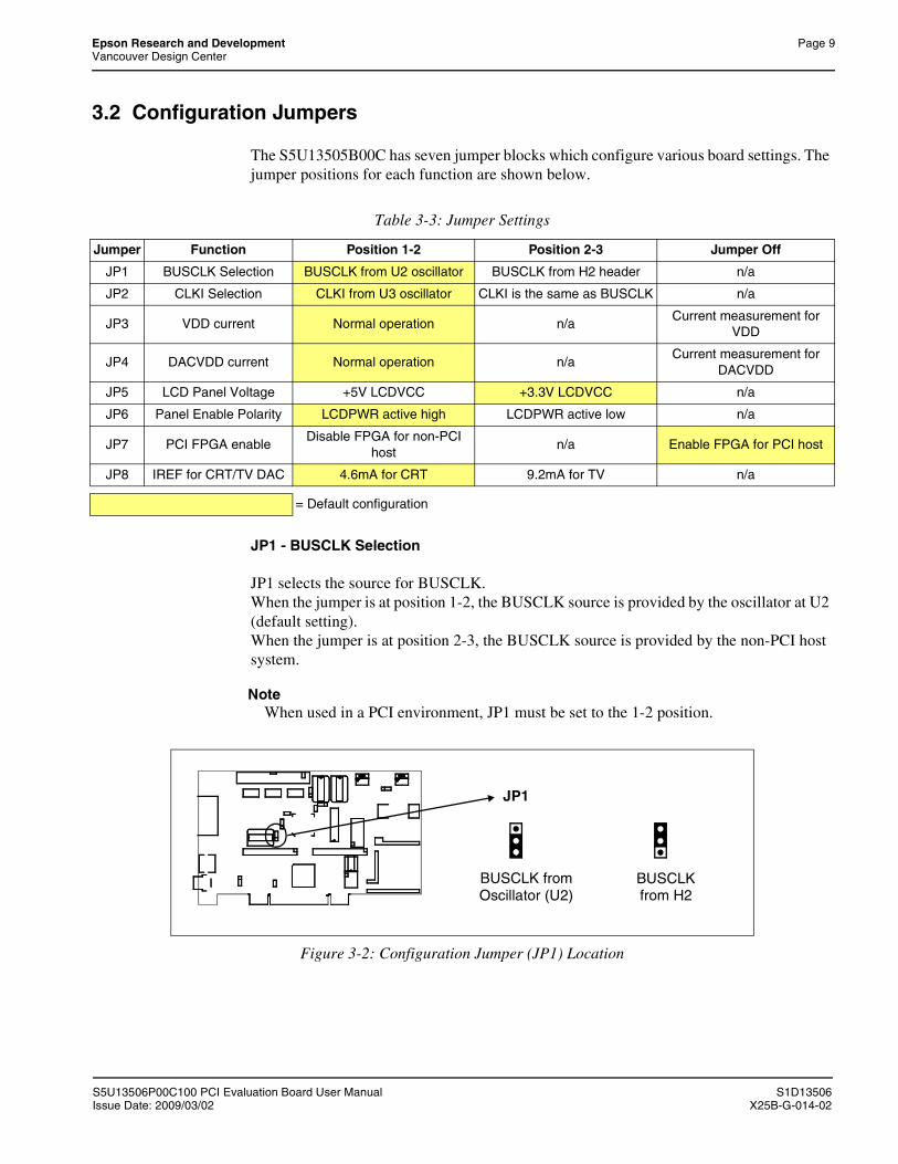
3.2 Configuration Jumpers
The S5U13505B00C has seven jumper blocks which configure various board settings. The jumper positions for each function are shown below.
JP1 - BUSCLK Selection
JP1 selects the source for BUSCLK.When the jumper is at position 1-2, the BUSCLK source is provided by the oscillator at U2 (default setting).When the jumper is at position 2-3, the BUSCLK source is provided by the non-PCI host system.
NoteWhen used in a PCI environment, JP1 must be set to the 1-2 position.
Figure 3-2: Configuration Jumper (JP1) Location
Table 3-3: Jumper Settings
Jumper Function Position 1-2 Position 2-3 Jumper Off
JP1 BUSCLK Selection BUSCLK from U2 oscillator BUSCLK from H2 header n/a
JP2 CLKI Selection CLKI from U3 oscillator CLKI is the same as BUSCLK n/a
JP3 VDD current Normal operation n/aCurrent measurement for
VDD
JP4 DACVDD current Normal operation n/aCurrent measurement for
DACVDD
JP5 LCD Panel Voltage +5V LCDVCC +3.3V LCDVCC n/a
JP6 Panel Enable Polarity LCDPWR active high LCDPWR active low n/a
JP7 PCI FPGA enableDisable FPGA for non-PCI
hostn/a Enable FPGA for PCI host
JP8 IREF for CRT/TV DAC 4.6mA for CRT 9.2mA for TV n/a
= Default configuration
JP1
BUSCLKBUSCLK fromOscillator (U2) from H2

Page 10 Epson Research and DevelopmentVancouver Design Center
S1D13506 S5U13506P00C100 PCI Evaluation Board User ManualX25B-G-014-02 Issue Date: 2009/03/02
JP2 - CLKI Selection
JP2 selects the source for CLKI.When the jumper is at position 1-2, the CLKI source is provided by the oscillator at U3 (default setting).When the jumper is at position 2-3, the CLKI source is the same as BUSCLK (provided by the non-PCI host system).
Figure 3-3: Configuration Jumper (JP2) Location
JP3 - VDD current
JP3 allows the measurement of S1D13505 VDD current consumption.When the jumper is at position 1-2, the evaluation board is operating normally (default setting).When no jumper is installed, VDD current consumption can be measured by connecting an ammeter to JP3.
Figure 3-4: Configuration Jumper (JP3) Location
JP2
CLKI fromOscillator (U3)
CLKI sameas BUSCLK
JP3
CoreVDDNormalOperation Measurement

Epson Research and Development Page 11Vancouver Design Center
S5U13506P00C100 PCI Evaluation Board User Manual S1D13506Issue Date: 2009/03/02 X25B-G-014-02
JP4 - DACVDD current
JP4 allows the measurement of S1D13505 DACVDD current consumption.When the jumper is at position 1-2, the evaluation board is operating normally (default setting).When no jumper is installed, DACVDD current consumption can be measured by connecting an ammeter to JP4.
Figure 3-5: Configuration Jumper (JP4) Location
JP5 - LCD panel voltage
JP5 selects the voltage level to the LCD panel.When the jumper is at position 1-2, the LCD panel voltage level is configured for 5.0V.When the jumper is at position 2-3, the LCD panel voltage level is configured for 3.3V (default setting).
Figure 3-6: Configuration Jumper (JP5) Location
JP4
CoreVDDNormalOperation Measurement
JP5
+3.3 LCDVCC+5V LCDVCC

Page 12 Epson Research and DevelopmentVancouver Design Center
S1D13506 S5U13506P00C100 PCI Evaluation Board User ManualX25B-G-014-02 Issue Date: 2009/03/02
JP6 - Panel Enable Polarity
JP6 selects the polarity of the LCDPWR panel enable signal.When the jumper is at position 1-2, the LCDPWR signal is active high (default setting).When the jumper is at position 2-3, the LCDPWR signal is active low.
Figure 3-7: Configuration Jumper (JP6) Location
JP7 - PCI FPGA Enable
JP7 controls the PCI FPGA.When no jumper is installed, the PCI FPGA is enabled and the evaluation board may be used in a PCI environment (default setting).When the jumper is in position 1-2, the PCI FPGA is disabled and the evaluation board may be used with a non-PCI host system.
NoteNon-PCI host system must be connected to headers H1 and H2.
Figure 3-8: Configuration Jumper (JP7) Location
JP6
LCDPWRActive High
LCDPWRActive Low
JP7
non-PCI(FPGA Disabled)
PCI(FPGA Enabled)

Epson Research and Development Page 13Vancouver Design Center
S5U13506P00C100 PCI Evaluation Board User Manual S1D13506Issue Date: 2009/03/02 X25B-G-014-02
JP8 - IREF for CRT/TV DAC
JP8 selects the magnitude of the IREF current used by the embedded RAMDAC.When the jumper is at position 1-2, the IREF current is 4.6mA. This setting is used for CRT display.When the jumper is at position 2-3, the IREF current is 9.2mA. This setting is used for TV display, but it may be used by CRT display as well.
Figure 3-9: Configuration Jumper (JP8) Location
JP8
IREF = 9.2mAIREF = 4.6mA

Page 14 Epson Research and DevelopmentVancouver Design Center
S1D13506 S5U13506P00C100 PCI Evaluation Board User ManualX25B-G-014-02 Issue Date: 2009/03/02
4 Technical Description
The S5U13506P00C100 operates with both PCI and non-PCI evaluation platforms. It supports passive LCD panels (4/6/16-bit), TFT/D-TFD panels (9/12/18-bit), CRT displays (analog RGB output) and TV (NTSC and PAL).
4.1 PCI Bus Support
The S5U13506P00C100 does not have on-chip PCI bus interface support. The S5U13506P00C100 uses the PCI FPGA to support the PCI bus.
4.2 Non-PCI Host Interface Support
The S5U13506P00C100 is specifically designed to support a standard PCI bus environment (using the PCI Bridge Adapter FPGA). However, the S5U13506P00C100 can directly support many other Host Bus Interfaces. When the FPGA is disabled (using jumper JP7), headers H1 and H2 provide the necessary IO pins to interface to the Host Bus Inter-faces listed in Table 4-4:, “CPU Interface Pin Mapping”.
NoteThe S5U13506P00C100 is designed to work only with 3.3V systems. To use it with a 5V system, some modifications must be done to the board as follows:
1. Replace the 3.3V DRAM (U6) on the board with a 5V DRAM.
2. Cut the trace between JP9-2 and JP9-3 on the solder side of the board.
3. Connect JP9-1 and JP9-2. This will set IOVDD to 5V.

Epson Research and Development Page 15Vancouver Design Center
S5U13506P00C100 PCI Evaluation Board User Manual S1D13506Issue Date: 2009/03/02 X25B-G-014-02
4.2.1 CPU Interface Pin Mapping
The functions of the S1D13506 host interface pins are mapped to each host bus interface according to the following table.
Note1 A0 for these busses is not used internally by the S1D13506.
Table 4-4: CPU Interface Pin Mapping
S1D13505Pin
NamesGeneric
HitachiSH-4/SH-3
MIPS/ISAMotorolaMC68KBus 1
MotorolaMC68KBus 2
MotorolaPowerPC
PC CardPhilips
PR31500/PR31700
ToshibaTX3912
AB20 A20 A20 LatchA20 A20 A20 A11 A20 ALE ALE
AB19 A19 A19 SA19 A19 A19 A12 A19 /CARDREG CARDREG*
AB18 A18 A18 SA18 A18 A18 A13 A18 /CARDIORD CARDIORD*
AB17 A17 A17 SA17 A17 A17 A14 A17 /CARDIOWR CARDIOWR*
AB[16:13] A[16:13] A[16:13] SA[16:13] A[16:13] A[16:13] A[15:18] A[16:13] Connected to VDD
AB[12:1] A[12:1] A[12:1] SA[12:1] A[12:1] A[12:1] A[19:30] A[12:1] A[12:1] A[12:1]
AB0 A01 A01 SA0 LDS# A0 A31 A01 A0 A0
DB[15:8] D[15:0] D[15:8] SD[15:0] D[15:8] D[31:24] D[0:7] D[15:0] D[23:16] D[23:16]
DB[7:0] D[7:0] D[7:0] SD[7:0] D[7:0] D[23:16] D[8:15] D[7:0] D[31:24] D[31:24]
WE1# WE1# WE1# SBHE# UDS# DS# BI -CE2 /CARDxCSH CARDxCSH*
M/R# External Decode Connected to VDD
CS# External Decode Connected to VDD
BUSCLK BCLK CKIO CLK CLK CLK CLKOUT CLK DCLKOUT DCLKOUT
BS# Connected to VDD
BS# Connected to VDD
AS# AS# TS Connected to VDD
Connected to VDD
RD/WR# RD1# RD/WR# Connected to VDD
R/W# R/W# RD/WR -CE1 /CARDxCSL CARDxCSL*
RD# RD0# RD# MEMR# Connected to VDD
SIZ1 TSIZ0 -OE /RD RD*
WE0# WE0# WE0# MEMW# Connected to VDD
SIZ0 TSIZ1 -WE /WE WE*
WAIT# WAIT#RDY#
/WAIT#IOCHRDY DTACK# DSACK1# TA -WAIT /CARDxWAIT CARDxWAIT*
RESET# RESET# RESET#invertedRESET
RESET# RESET# RESET#invertedRESET
RESET# PON*

Page 16 Epson Research and DevelopmentVancouver Design Center
S1D13506 S5U13506P00C100 PCI Evaluation Board User ManualX25B-G-014-02 Issue Date: 2009/03/02
4.2.2 CPU Bus Connector Pin Mapping
The pinouts for Connector H1 are listed in the following table.
Table 4-5: CPU/BUS Connector (H1) Pinout
Pin No. Function1 Connected to DB0 of the S1D135062 Connected to DB1 of the S1D13506
3 Connected to DB2 of the S1D135064 Connected to DB3 of the S1D135065 Ground
6 Ground7 Connected to DB4 of the S1D135068 Connected to DB5 of the S1D13506
9 Connected to DB6 of the S1D1350610 Connected to DB7 of the S1D1350611 Ground
12 Ground13 Connected to DB8 of the S1D1350614 Connected to DB9 of the S1D13506
15 Connected to DB10 of the S1D1350616 Connected to DB11 of the S1D1350617 Ground
18 Ground19 Connected to DB12 of the S1D1350620 Connected to DB13 of the S1D13506
21 Connected to DB14 of the S1D1350622 Connected to DB15 of the S1D1350623 Connected to RESET# of the S1D13506
24 Ground25 Ground26 Ground
27 +12 volt supply, required in non-PCI applications28 +12 volt supply, required in non-PCI applications29 Connected to WE0# of the S1D13506
30 Connected to WAIT# of the S1D1350631 Connected to CS# of the S1D1350632 Connected to MR# of the S1D13506
33 Connected to WE1# of the S1D13506534 S1D13506 supply, provided by the S5U13506P00C100

Epson Research and Development Page 17Vancouver Design Center
S5U13506P00C100 PCI Evaluation Board User Manual S1D13506Issue Date: 2009/03/02 X25B-G-014-02
The pinouts for Connector H2 are listed in the following table.
Table 4-6: CPU/BUS Connector (H2) Pinout
Pin No. Function
1 Connected to AB0 of the S1D13506
2 Connected to AB1 of the S1D13506
3 Connected to AB2 of the S1D13506
4 Connected to AB3 of the S1D13506
5 Connected to AB4 of the S1D13506
6 Connected to AB5 of the S1D13506
7 Connected to AB6 of the S1D13506
8 Connected to AB7 of the S1D13506
9 Ground
10 Ground
11 Connected to AB8 of the S1D13506
12 Connected to AB9 of the S1D13506
13 Connected to AB10 of the S1D13506
14 Connected to AB11 of the S1D13506
15 Connected to AB12 of the S1D13506
16 Connected to AB13 of the S1D13506
17 Ground
18 Ground
19 Connected to AB14 of the S1D13506
20 Connected to AB15 of the S1D13506
21 Connected to AB16 of the S1D13506
22 Connected to AB17 of the S1D13506
23 Connected to AB18 of the S1D13506
24 Connected to AB19 of the S1D13506
25 Ground
26 Ground
27 +5 volt supply, required in non-PCI applications
28 +5 volt supply, required in non-PCI applications
29 Connected to RD/WR# of the S1D13506
30 Connected to BS# of the S1D13506
31 Connected to S1D13506 BUSCLK if JP1 is in position 2-3
32 Connected to RD# of the S1D13506
33 Connected to AB20 of the S1D13506
34 Not connected

Page 18 Epson Research and DevelopmentVancouver Design Center
S1D13506 S5U13506P00C100 PCI Evaluation Board User ManualX25B-G-014-02 Issue Date: 2009/03/02
4.3 LCD Support
The S1D13506 supports 4/8-bit dual and single passive monochrome panels, 4/8/16-bit dual and single passive color panels, and 9/12/18-bit active matrix color TFT/D-TFD panels. All necessary signals are provided on the 40-pin LCD connector (J1). The interface signals are alternated with grounds on the cable to reduce cross-talk and noise. When supporting an 18-bit TFT/D-TFD panel, the S1D13505 can display 64K of a possible 256K colors because only 16 of the18 bits of LCD data are available from the S1D13505. For details, refer to the S1D13506 Hardware Functional Specification, document number X25B-A-001-xx.
For S1D13506 FPDAT[15:0] pin mapping for various types of panel see Table 4-7:, “LCD Signal Connector (J4)” on page 19.

Epson Research and Development Page 19Vancouver Design Center
S5U13506P00C100 PCI Evaluation Board User Manual S1D13506Issue Date: 2009/03/02 X25B-G-014-02
4.3.1 LCD Interface Pin Mapping
Note1 For FPDATxx to LCD interface hardware connections refer to the Display Interface
AC Timing section of the S1D13506 Hardware Functional Specification, documentnumber X25B-A-001-xx.
2 The S5U13506B00C was designed using S1D13506 pin 75 (LCDPWR) to control theLCD bias power. This design is no longer supported. Applications should use one ofthe available GPIO pins to control the LCD bias power allowing for software controlof power sequencing delays. For further information on LCD power sequencing, seethe S1D13506 Programming Notes and Examples, document number X25B-G-003-
xx.
Table 4-7: LCD Signal Connector (J4)
S1D13505Pin Names
ConnectorPin No.
Monochrome Passive Panels
Color Passive PanelsColor TFT/D-TFD
Panels Single Dual Single
SingleFormat 1
SingleFormat 2
Single Dual
4-bit 8-bit 8-bit 4-bit 8-bit 8-bit 16-Bit 8-bit 16-bit 9-bit 12-bit 18-bitFPDAT0 1 and 6 D0 LD0 D0 D0 D0 LD0 LD0 R2 R3 R5
FPDAT1 3 D1 LD1 D1 D1 D1 LD1 LD1 R1 R2 R4FPDAT2 5 D2 LD2 D2 D2 D2 LD2 LD2 R0 R1 R3FPDAT3 7 D3 LD3 D3 D3 D3 LD3 LD3 G2 G3 G5
FPDAT4 9 D0 D4 UD0 D0 D4 D4 D8 UD0 UD0 G1 G2 G4FPDAT5 11 D1 D5 UD1 D1 D5 D5 D9 UD1 UD1 G0 G1 G3FPDAT6 13 and 4 D2 D6 UD2 D2 D6 D6 D10 UD2 UD2 B2 B3 B5
FPDAT7 15 D3 D7 UD3 D3 D7 D7 D11 UD3 UD3 B1 B2 B4FPDAT8 17 D4 LD4 B0 B1 B3FPDAT9 19 D5 LD5 R0 R2
FPDAT10 21 D6 LD6 R1FPDAT11 23 D7 LD7 G0 G2FPDAT12 25 D12 UD4 G1
FPDAT13 27 D13 UD5 G0FPDAT14 29 D14 UD6 B0 B2FPDAT15 31 D15 UD7 B1
FPSHIFT 33 FPSHIFTDRDY 35 and 38 MOD FPSHIFT2 MOD DRDY
FPLINE 37 FPLINE
FPFRAME 39 FPFRAME
GND2 and 8-26(Even Pins)
GND
N/C 28 N/CN/C 30 N/C
LCDVCC 32 +5V or +3.3V according to JP5+12V 34 +12VN/C 36 N/C
NC (pin 75)2 40 Panel Enable, active low (LCDPWR)2
= Driven low

Page 20 Epson Research and DevelopmentVancouver Design Center
S1D13506 S5U13506P00C100 PCI Evaluation Board User ManualX25B-G-014-02 Issue Date: 2009/03/02
4.3.2 Buffered LCD Connector
J4 provides the same LCD panel signals as those directly from S1D13505, but with voltage-adapting buffers which can be set to 3.3V or 5V. Pin 32 on this connector provides power for the LCD panel logic at the same voltage as the buffer power supply.

Epson Research and Development Page 21Vancouver Design Center
S5U13506P00C100 PCI Evaluation Board User Manual S1D13506Issue Date: 2009/03/02 X25B-G-014-02
4.4 CRT/TV Support
4.4.1 CRT/TV Interface Pin Mapping
CRT/TV signals are supplied on a standard CRT connector (J2), Composite Video connector (J1), and S-Video connector (J3):
4.4.2 CRT Support
CRT support is provided on connector J2 via the S1D13506 embedded RAMDAC. An external current reference is implemented to provide the necessary RAMDAC output gain. The reference current (IREF) should be set to 4.6mA using jumper JP8.
NoteWhen IREF is set to 4.6mA, the DAC Output Select bit (REG[05Bh] bit 3) must be set to 1.
CRT output is not available when TV output is enabled.
4.4.3 TV Support
The S1D13506 supports PAL or NTSC TV output. Composite Video is available on connector J1 and S-Video is available on connector J3. An external current reference is implemented to provide the necessary RAMDAC output gain. The reference current should be set to 9.2mA using jumper JP8.
TV output is not available when CRT output is enabled. PAL and NTSC modes cannot be enabled at the same time.
4.5 Current consumption measurement
The evaluation board has 2 headers, JP3 and JP4, which allow the independent measurement of S1D13506 VDD and DACVDD current consumption. To measure the current, remove the appropriate jumper and connect an ammeter to the corresponding header pins.
Table 4-8: CRT/TV Interface Pin Mapping
S1D13506Pin Name
CRT Composite Video S-Video
HRTC Horizontal retrace N/A N/A
VRTC Vertical retrace N/A N/A
RED Red N/A Luminance
GREEN Green Composite N/A
BLUE Blue N/A Chrominance

Page 22 Epson Research and DevelopmentVancouver Design Center
S1D13506 S5U13506P00C100 PCI Evaluation Board User ManualX25B-G-014-02 Issue Date: 2009/03/02
5 References
5.1 Documents
• Epson Research and Development, Inc., S1D13506 Hardware Functional Specification, Document Number X25B-A-001-xx.
• Epson Research and Development, Inc., S1D13506 Programming Notes and Examples, Document Number X25B-G-003-xx.
5.2 Document Sources
• Epson Research and Development Website: http://www.erd.epson.com.

Epson Research and Development Page 23Vancouver Design Center
S5U13506P00C100 PCI Evaluation Board User Manual S1D13506Issue Date: 2009/03/02 X25B-G-014-02
6 Parts ListItem Quantity Reference Part Footprint Comments
1 38
C1,C2,C3,C4,C5,C6, C7,C8,C9,C10,C11, C12,C13,C16,C17, C18,C19,C20,C22, C23,C24,C27,C29, C30,C31,C40,C41, C42,C43,C44,C45, C46,C47,C48,C49,
C50,C51,C52
0.1uF C0805 Kemet C0805C104K4RACTU generic
2 6C14,C15,C21,C36,
C37,C3868uF/10V/10% — Kemet T491D686K010AS or equivalent
3 2 C35,C39 33uF/20V/10% — Kemet T491D336K020AS or equivalent
4 3 D1,D2,D3 BAV99 SOT23 Fairchild Semiconductor BAV99
5 2 H1,H2 HEADER 17X2 HDR2X17Thomas&Betts 609-3407 altern.
Samtec TSW-117-05-G-D or equiv.
6 5 JP1,JP2,JP5,JP6,JP8Header 3x1, 0.1" pitch,
unshroudedSIP3 —
7 3 JP3,JP4,JP7Header 2x1, 0.1" pitch,
unshroudedSIP2 —
8 1 J1 C-VIDEO — CUI RCJ-014
9 1 J2VGA
CONNECTORDB15/PS2CO
NNorComp 181-015-213R561 or equivalent
105 1 J3 S-VIDEO —Kycon KMDGX-4S-BS-99 or equivalent Mini DIN
4 pin
11 1 J4 CON40A HDR2X20A Samtec TST-120-01-G-D or equivalent
12 5 L1,L2,L3,L4,L5 Ferrite Bead INDUCTOR1 Steward 28F0181-ISR-10
13 1 Q1 MMBT2222A SOT23Fairchild Semiconductor MMBT2222A or
equivalent
14 3 R1,R2,R36 100K,5% R0805 —
15 3 R4,R5,R6 150R,1% R0805 generic
16 1 R7 0R R0805 —
17 16
R9,R10,R11,R12,R13,R14,R15,R16,R17, R18,R20,R39,R40,
R41,R42,R44
15K,5% R0805 —
18 1 R19 1.5K,1% R0805 generic
19 4 R21,R37,R38,R43 1K,1% R0805 —
20 1 R23 69.8R,1% R0805 —
21 1 R24 140R,1% R0805 generic
22 1 S1 SW DIP-8 DIPSW8 Grayhill 76SB08S
23 1 U1 S1D13506F00A TQFP128 Epson S1D13506F00A
24 1 U2 40MHz DIP14 Epson SG8002DB, 40MHz socketed
25 1 U3 25.175MHz DIP14 Epson SG8002DB, 25MHz socketed

Page 24 Epson Research and DevelopmentVancouver Design Center
S1D13506 S5U13506P00C100 PCI Evaluation Board User ManualX25B-G-014-02 Issue Date: 2009/03/02
26 1 U4 14.31818MHz DIP14 Epson SG8002DB, 14.31818MHz socketed
27 1 U5 LT1117CM-3.3 DDPAK-2 Linear Technologies LT1117CM-3.3
28 1 U6DRAM 1Mx16-SOJ, Lead free
SOJ42 ISSI IS41LV16100B-50KL
29 1 U7 LT1117CST-3.3 — Linear Technologies LT1117CST-3.3
30 1 U8INVERTER
SINGLE NC7S04
SC70-5 Fairchild Semiconductor NC7S04P5
31 3 U9,U10,U11 74AHC244 SO20W TI 74AHC244
32 1 U14EPF6016TC14
4-2TQFP144 Altera EPF6016TC144-2
33 1 U15 EPC1PI8N DIP8 Altera EPC1PI8N programmed, socketed
Item Quantity Reference Part Footprint Comments

Epson Research and Development Page 25Vancouver Design Center
S5U13506P00C100 PCI Evaluation Board User Manual S1D13506Issue Date: 2009/03/02 X25B-G-014-02
7 Schematic Diagrams
Figure 7-1: S5U13506P00C100 Evaluation Board Schematics (1 of 5)
1 1
2 2
3 3
4 4
5 5
6 6
7 7
8 8
AA
BB
CC
DD
MA
[9..0
]
MA
4
MA
2
MA
8
MA
5
MA
3
MA
1M
A0
MA
7M
A6
DB0
DB1
DB2
DB3
DB4
DB5
DB8
DB9
DB1
0D
B11
DB1
2D
B13
DB1
4D
B15
FPD
AT2
FPD
AT3
FPD
AT4
FPD
AT8
FPD
AT9
DB6
DB7
FPD
AT1
0
FPD
AT0
FPD
AT1
FPD
AT[
15..0
]
FPD
AT1
1FP
DA
T12
FPD
AT1
3FP
DA
T14
FPD
AT1
5
FPD
AT5
FPD
AT6
FPD
AT7
AB
6
AB
4
AB
15
AB
3
AB
18
AB
7
AB
11
AB
16
AB
12
AB
14
AB
8
AB
10A
B9
AB
0
AB
17
AB
19
AB
13
AB
1
AB
5
AB
2
AB[
20:0
]
DB
[15:
0]
MA
9M
A10
AB
20
MD
15
MD
8
MD
13
MD
2M
D1
MD
5
MD
12
MD
6M
D7
MD
4
MD
10M
D11
MD
0
MD
9
MD
14
MD
3
MA
11
MD
[15.
.0]
3.3V
IOV
DD
IOVD
D
DAC
VDD
IOV
DD
IOVD
DD
AC
VD
D
+3.3
V+5
V
+5V
IOVD
D
+3.3
V
IOVD
D
IOVD
D
IOVD
D
AB[
20:0
]4,
5
DB
[15:
0]4,
5
MA
[9..0
]2
RA
S#2
LCA
S#
2U
CA
S#
2W
E#2
LCD
PWR
#3
FPFR
AME
3FP
LIN
E3
FPS
HIF
T3
DR
DY
3FP
DAT
[15.
.0]
3
RD
/WR
#4,
5W
E1#
4,5
WE0
#4,
5R
D#
4,5
BS#
4,5
RE
SET
#4,
5
M/R
#4,
5
CS
#4,
5
WAI
T#4,
5
MD
[15.
.0]
2
BU
SC
LK
RE
D2
GR
EEN
2
BLU
E2
HR
TC2
VRTC
2
CLK
I
IRE
F2
CLK
I
FPG
A_C
LK5
BU
SC
LK
BCLK
4
BUSC
LK
CLK
I2
CLK
I2
Siz
eD
ocum
ent N
umbe
rR
ev
Dat
e:S
heet
of
2.0
Eps
on R
esea
rch
& D
evel
opm
ent,
Inc.
S5U
1350
5/6B
00C
PC
I Bus
: 135
06F0
0A C
hip
Cus
tom
15
Mon
day,
Dec
embe
r 11,
200
6
Siz
eD
ocum
ent N
umbe
rR
ev
Dat
e:S
heet
of
2.0
Eps
on R
esea
rch
& D
evel
opm
ent,
Inc.
S5U
1350
5/6B
00C
PC
I Bus
: 135
06F0
0A C
hip
Cus
tom
15
Mon
day,
Dec
embe
r 11,
200
6
Siz
eD
ocum
ent N
umbe
rR
ev
Dat
e:S
heet
of
2.0
Eps
on R
esea
rch
& D
evel
opm
ent,
Inc.
S5U
1350
5/6B
00C
PC
I Bus
: 135
06F0
0A C
hip
Cus
tom
15
Mon
day,
Dec
embe
r 11,
200
6
CO
REV
DD
By-
pass
Cap
acito
rs (1
/pow
er p
in)
DA
CV
DD
By-
pass
Cap
acito
rs (1
/pow
er p
in)
Sho
rt pi
n 2
and
3 of
JP
8 on
PC
B, s
olde
r sid
e.
Not
pop
ulat
ed fo
r S5U
1350
5B00
C
Not
pop
ulat
ed
Not
pop
ulat
ed
C8
0.1u
F
C8
0.1u
F
AB
03
AB
12
AB
21
AB
312
8
AB
412
7
AB
512
6
AB
612
5A
B7
124
AB
812
3
AB
912
2A
B10
121
AB
1112
0A
B12
119
AB
1311
8A
B14
117
AB
1511
6
AB
1611
5
MA
061
MA
163
MA
265
MA
367
MA
466
MA
564
MA
662
MA
760
MD
035
MD
137
MD
239
MD
341
MD
443
MD
545
MD
647
MD
749
MD
848
MD
946
MD
1044
MD
1240
MD
1338
FPFR
AM
E73
FPLI
NE
74
FPS
HIF
T77
FPD
AT0
79FP
DA
T180
FPD
AT2
81FP
DA
T382
FPD
AT5
84FP
DA
T685
FPD
AT7
86
AB
1711
4A
B18
113
AB
1911
2
M/R
#5
CS
#4
MA
858
LCD
PW
R75
VS
S1
14
VS
S2
32
VS
S4
68
VS
S7
96
MA
9/G
PIO
356
VS
S6
87V
SS
578
AB
2011
1
DR
DY
76
FPD
AT1
292
FPD
AT1
393
FPD
AT1
494
FPD
AT1
595
VS
S3
50
VS
S8
110
MA
10/G
PIO
159
MD
1142
MA
11/G
PIO
257
MD
1436
MD
1534
DB
031
DB
130
DB
229
DB
328
DB
427
DB
526
DB
625
DB
724
DB
823
DB
922
DB
1021
DB
1120
DB
1219
DB
1318
DB
1417
DB
1516
RA
S#
54LC
AS
#51
UC
AS
#52
WE
#53
FPD
AT8
88
FPD
AT1
090
FPD
AT1
191
FPD
AT9
89
FPD
AT4
83
HR
TC10
7
VR
TC10
8
RE
D10
0
GR
EE
N10
3
BLU
E10
5
IRE
F10
1
RD
/WR
#10
WE
1#9
WE
0#8
RD
#7
BS
#6
RE
SE
T#11
CLK
I69
BU
SC
LK13
WA
IT#
15
TES
TEN
70
VD
D1
12V
DD
233
VD
D3
55
VD
D4
72
VD
D5
97
VD
D6
109
DA
C_V
SS
198
DA
C_V
SS
210
6
DA
C_V
DD
199
DA
C_V
DD
210
2
CLK
I271
DA
C_V
DD
310
4
U1
S1D
1350
6F00
A
U1
S1D
1350
6F00
A
C16
0.1u
FC
160.
1uF
C4
0.1u
F
C4
0.1u
F
R3
100K
,5%
R3
100K
,5%
11 22
JP4
DA
C C
UR
RE
NT
JP4
DA
C C
UR
RE
NT
C10
0.1u
F
C10
0.1u
F
C13
0.1u
F
C13
0.1u
F
C6
0.1u
F
C6
0.1u
F
1 2 3
JP1
BUSC
LK
JP1
BUSC
LK
C5
0.1u
F
C5
0.1u
F
C11
0.1u
F
C11
0.1u
F
R2
100K
,5%
R2
100K
,5%
VIN
3
ADJ 1
VO
UT
2
U5
LT11
17C
M-3
.3U
5LT
1117
CM
-3.3
C2
0.1u
F
C2
0.1u
F
L2 FER
RIT
E B
EAD
L2 FER
RIT
E B
EAD
C1
0.1u
F
C1
0.1u
F
+C
1568
uF/1
0V/1
0%+
C15
68uF
/10V
/10%
+C
1468
uF/1
0V/1
0%+
C14
68uF
/10V
/10%
R1
100K
,5%
R1
100K
,5%
C3
0.1u
F
C3
0.1u
F
123
JP2
CLK
I
JP2
CLK
I
NC
1
OU
T8
GN
D7
VC
C14
U4
14.3
1818
MH
zU
414
.318
18M
Hz
C7
0.1u
F
C7
0.1u
F
C12
0.1u
F
C12
0.1u
F
123
JP9
IOV
DD
SE
LEC
TJP
9IO
VD
D S
ELE
CT
C9
0.1u
F
C9
0.1u
F
L1 FER
RIT
E B
EAD
L1 FER
RIT
E B
EAD
NC
1
OU
T8
GN
D7
VC
C14
U2
40M
Hz
U2
40M
Hz NC
1
OU
T8
GN
D7
VC
C14
U3
25.1
75M
Hz
U3
25.1
75M
Hz
11 22
JP3
CO
RE
/IO C
UR
RE
NT
JP3
CO
RE
/IO C
UR
RE
NT

Page 26 Epson Research and DevelopmentVancouver Design Center
S1D13506 S5U13506P00C100 PCI Evaluation Board User ManualX25B-G-014-02 Issue Date: 2009/03/02
Figure 7-2: S5U13506P00C100 Evaluation Board Schematics (2 of 5)
1 1
2 2
3 3
4 4
5 5
6 6
7 7
8 8
AA
BB
CC
DD
Con
fig s
etup
for S
1D13
505:
MD
0 - 1
=8bi
t, 0=
16bi
tM
D[3
:1]=
sel
ects
CP
U b
us in
terfa
ceM
D4
- 1=L
ittle
End
ian,
0=B
ig E
ndia
nM
D5
- 1=W
AIT
# A
CTI
VE
HIG
H, 0
=WA
IT#A
CTI
VE
LO
WM
D[7
:6] -
Mem
ory
type
set
for S
ymet
rical
1M
x16D
RA
MM
D8
- not
use
dM
D9
- 1=S
US
PE
ND
PIN
as
GP
OM
D10
- ac
tive
LOW
LC
DP
WR
/act
ive
HIG
H G
PO
MD
[15:
13] -
not
use
d
Not
e: C
hip
has
inte
rnal
tie
low
resi
stor
s
MD
12 -
1=B
US
CLK
inpu
t div
ide,
0=n
o di
vide
MD
11 -
1=A
ltern
ate,
0=P
rimar
y H
ost S
elec
tion
Not
pop
ulat
ed fo
r S5U
1350
5B00
C
Not
pop
ulat
ed fo
r S5U
1350
5B00
C
Not
pop
ulat
ed fo
r S5U
1350
5B00
C
Not
pop
ulat
ed fo
r S5U
1350
6B00
C
Not
pop
ulat
ed fo
rS
5U13
506B
00C
MD
[14:
13] -
not
use
d
MD
10 -
not u
sed,
but
set
to b
e ac
tive
LOW
LC
DP
WR
(pin
75
NC
)M
D9
- 1=S
US
PE
ND
PIN
as
GP
OM
D8
- not
use
dM
D[7
:6] -
Mem
ory
type
set
for S
ymet
rical
1M
x16D
RA
MM
D5
- 1=W
AIT
# A
CTI
VE
HIG
H, 0
=WA
IT#A
CTI
VE
LO
W
Con
fig s
etup
for S
1D13
506:
MD
4 - 1
=Litt
le E
ndia
n, 0
=Big
End
ian
MD
[3:1
]= s
elec
ts C
PU
bus
inte
rface
MD
0 - n
ot u
sed
MD
11 -
1=A
ltern
ate,
0=P
rimar
y H
ost S
elec
tion
MD
12 -
1=B
US
CLK
inpu
t div
ide,
0=n
o di
vide
MD
15 -
1=W
AIT
# al
way
s dr
iven
, 0=W
AIT
# is
tris
tate
d
Not
e: C
hip
has
inte
rnal
tie
low
resi
stor
s
2.0
S5U
1350
5/6B
00C
PC
I Bus
: DR
AM
/Con
figur
atio
n/C
RT
Out
put
25
Thur
sday
, Oct
ober
03,
200
2BE
pson
Res
earc
h &
Dev
elop
men
t, In
c.Ti
tle
Siz
eD
ocum
ent N
umbe
rR
ev
Dat
e:S
heet
of
MA
[9..0
]
MD
[15.
.0] M
A5
MA
8
MA
6
MA
4
MA
2M
A3
MA
1
MA
7
MA
0
MA
9
MD
2
MD
11
MD
0
MD
6
MD
2
MD
11
MD
9
MD
0
MD
13
MD
3M
D4
MD
15
MD
[15.
.0]
MD
1
MD
7M
D6
MD
4
MD
10
MD
10
MD
3
MD
9
MD
14
MD
8
MD
12
MD
5
MD
1
MD
5
MD
12
MD
15
MD
[15.
.0]
1
MA
[9..0
]1
RAS
#1
UC
AS
#1
LCA
S#
1
WE
#1 M
D[1
5..0
]1
RE
D1
GR
EE
N1
BLU
E1
HR
TC1
VR
TC1
IRE
F1
IOV
DD
DA
CV
DD
DA
CV
DD
DA
CVD
D
IOV
DD
+5V
R17
15K
,5%
J2 VG
A C
ON
NE
CTO
R
6 1 11 7 2 12 8 3 13 9 4 14 10 5 15
D3
BAV
99
1
3
2
D2
BA
V99
1
3
2
R13
15K
,5%
D1
BA
V99
1
3
2
C20
0.1u
F+
C21
68uF
/10V
/10%
R4
150R
,1%
R6
150R
,1%
C17
0.1u
F
L3FE
RR
ITE
BE
AD
R18
15K
,5%
L4FE
RR
ITE
BEA
D
R14
15K
,5%
U6
DR
AM
1M
x16-
SO
J
17 18 19 20 23 24 25 26 27 28 16 15 14 30 31 13 11 12 32 29
2 3 4 5 7 8 9 10 33 34 35 36 38 39 40 41 1 6 21 22 37 42
A0
A1
A2
A3
A4
A5
A6
A7
A8R
/A8
A9R
/A9
NC
NC
/RA
S/U
CA
S/L
CA
S
/W NC
NC
NC
/OE
DQ
0D
Q1
DQ
2D
Q3
DQ
4D
Q5
DQ
6D
Q7
DQ
8D
Q9
DQ
10D
Q11
DQ
12D
Q13
DQ
14D
Q15
VC
CV
CC
VC
C
VSS
VSS
VSS
R10
15K
,5%
U7
LT11
17C
ST-
3.3
3
1
2V
IN
ADJ
VO
UT
L5FE
RR
ITE
BE
AD
R19
1.5K
,1%
C18
0.1u
F
R23
69.8
R,1
%
R8
0RS
1
SW
DIP
-8
1 2 3 4 5 6 7 8
16 15 14 13 12 11 10 9
R20
15K
,5%
R7
0R
JP8
IRE
F
123
R5
150R
,1%
R15
15K
,5%
R11
15K
,5%
R21
1K,1
%
R9
15K
,5%
C19
0.1u
F
J1
C-V
IDE
O1
2 CY
GG
J3
S-V
IDE
O
43 1
2
R16
15K
,5%
R12
15K
,5%
R22
0R
Q1
MM
BT2
222A
3
1
2 R24
140R
,1%

Epson Research and Development Page 27Vancouver Design Center
S5U13506P00C100 PCI Evaluation Board User Manual S1D13506Issue Date: 2009/03/02 X25B-G-014-02
Figure 7-3: S5U13506P00C100 Evaluation Board Schematics (3 of 5)
1 1
2 2
3 3
4 4
5 5
6 6
7 7
8 8
AA
BB
CC
DD
FPD
1
FPS
2
FPD
7
FPD
5
FPD
AT4
FPD
3
FPD
AT1
0
FPD
AT6
FPD
AT1
4
FPD
AT3
FPD
15
FPD
AT5
FPD
AT9
FPD
AT1
FPD
AT8
FPD
AT2
FPD
AT[
15..0
]
FPD
AT1
2
FPD
2
FPD
AT0
FPD
0
FPD
AT1
5
FPD
AT1
1
FPD
AT1
3
FPD
6
FPD
AT7
FPD
4
FPD
13FP
D12
FPD
11
FPD
14
FPD
10
FPS
FPL
FPF
LCD
P#
FPD
9FP
D8
LCD
PW
R
FPD
6FP
D0
+12V
VD
DH
VLC
D
LCD
VC
C
LCD
VC
C
LCD
VC
C
LCD
VC
C
+5V
+3.3
V
LCD
VC
C
IOV
DD
IOV
DD
FPS
HIF
T1
DR
DY
1FP
LIN
E1
FPFR
AM
E1
FPD
AT[
15..0
]1
LCD
PO
WE
R
LCD
PW
R#
1
LCD
PO
WE
R
Siz
eD
ocum
ent N
umbe
rR
ev
Dat
e:S
heet
of
2.0
Eps
on R
esea
rch
& D
evel
opm
ent,
Inc.
S5U
1350
5/6B
00C
PC
I Bus
: LC
D H
eade
rs
B
35
Mon
day,
Dec
embe
r 11,
200
6
Siz
eD
ocum
ent N
umbe
rR
ev
Dat
e:S
heet
of
2.0
Eps
on R
esea
rch
& D
evel
opm
ent,
Inc.
S5U
1350
5/6B
00C
PC
I Bus
: LC
D H
eade
rs
B
35
Mon
day,
Dec
embe
r 11,
200
6
Siz
eD
ocum
ent N
umbe
rR
ev
Dat
e:S
heet
of
2.0
Eps
on R
esea
rch
& D
evel
opm
ent,
Inc.
S5U
1350
5/6B
00C
PC
I Bus
: LC
D H
eade
rs
B
35
Mon
day,
Dec
embe
r 11,
200
6CO
LOR
/MO
NO
LC
D C
ON
NE
CTO
R
Not
e: 2
44 in
put s
ide
viol
ates
the
spec
of c
hip.
At
5V, 2
44 lo
gic
high
nee
ds to
be
grea
ter t
han
3.7V
. O
urch
ip if
set
for 3
.3V
will
not
mee
t thi
s in
put
requ
irem
ent o
f the
244
.
Inpu
t on
244
can
take
upt
o 5.
5V a
s in
put h
igh.
1 2 3
JP6
LCD
PW
R S
ELE
CT
JP6
LCD
PW
R S
ELE
CT
1 3 5 7 9 11 13 15 17 19 21 23 25 27 29 31 33 35 37 39
2 4 6 8 10 12 14 16 18 20 22 24 26 28 30 32 34 36 38 40
J4 CO
N40
A
J4 CO
N40
A
1A1
21Y
118
1A2
41Y
216
1A3
61Y
314
1A4
81Y
412
2A1
112Y
19
2A2
132Y
27
2A3
152Y
35
2A4
172Y
43
1G1
2G19
VC
C20
GN
D10
U9
74AH
C24
4
U9
74AH
C24
4
1A1
21Y
118
1A2
41Y
216
1A3
61Y
314
1A4
81Y
412
2A1
112Y
19
2A2
132Y
27
2A3
152Y
35
2A4
172Y
43
1G1
2G19
VC
C20
GN
D10
U10
74AH
C24
4
U10
74AH
C24
4
C29
0.1u
F
C29
0.1u
F
C24
0.1u
F
C24
0.1u
F
123JP
5LC
D V
CC
SE
LEC
TJP
5LC
D V
CC
SE
LEC
T
C23
0.1u
F
C23
0.1u
F
Vcc
5
GN
D3
NC
1
A2
Y4
U8
INV
ER
TER
SIN
GLE
NC
7S04
U8
INV
ER
TER
SIN
GLE
NC
7S04
C22
0.1u
F
C22
0.1u
F
1A1
21Y
118
1A2
41Y
216
1A3
61Y
314
1A4
81Y
412
2A1
112Y
19
2A2
132Y
27
2A3
152Y
35
2A4
172Y
43
1G1
2G19
VC
C20
GN
D10
U11
74AH
C24
4
U11
74AH
C24
4

Page 28 Epson Research and DevelopmentVancouver Design Center
S1D13506 S5U13506P00C100 PCI Evaluation Board User ManualX25B-G-014-02 Issue Date: 2009/03/02
Figure 7-4: S5U13506P00C100 Evaluation Board Schematics (4 of 5)
1 1
2 2
3 3
4 4
5 5
6 6
7 7
8 8
AA
BB
CC
DD
IOV
DD
pro
vide
d by
the
SD
U13
505B
00C
2.0
Eps
on R
esea
rch
& D
evel
opm
ent,
Inc.
S5U
1350
5/6B
00C
PC
I Bus
: PC
I/Gen
eric
Hea
ders
B
45
Thur
sday
, Sep
tem
ber 1
9, 2
002
Siz
eD
ocum
ent N
umbe
rR
ev
Dat
e:S
heet
of
AB
8
DB
0
AB
5
AD
31
DB
3
AB
3A
D22
AD
23
DB
13
AB
17
AD
20
DB
5
DB
15
AD
25
AB
18
AB
2
AD
3
AD
6
AD
28
DB
7
AB
1
AD
8
AB
20
AB
15
AD
9
AD
14
AB
11
AD
5
DB
10D
B11
AD
11
AB
14
DB
14
AD
2
AD
26
AD[3
1:0]
AB
13
AB
7
AD
1
AB
0
AD
4
AD
12
AD
18
AD
0
AB
12
DB
12
AB
6A
D17
AB
[20:
0]
DB
[15:
0]
AD
29
DB
1
AB
19
AD
19
AB
10
AD
13
DB
9
AD
16
AB
4
AD
7
AD
10
DB
2
AB
9
AD
15
DB
6
DB
8
AB
16
AD
21
AD
24
AD
27
AD
30
DB
4
AB
[20:
0]1,
5
STO
P#5
FRA
ME#
5
TRD
Y#
5
PA
R5
RD
/WR
#1,
5
C/B
E0#
5
WA
IT#
1,5
IDS
EL
5
RE
SE
T#1,
5
RD
#1,
5C
/BE
1#5
C/B
E2#
5
CLK
5
WE
1#1,
5
BS
#1,
5
M/R
#1,
5C
S#
1,5
IRD
Y#
5
RS
T#5
SE
RR
#5
AD
[31:
0]5
BC
LK1
DB
[15:
0]1,
5
C/B
E3#
5
WE
0#1,
5
PE
RR
#5
DE
VS
EL#
5
+12V
+5V
+12V
IOV
DD
+5V
+5V
+5V
+12V +5
V+5
V
+5V
+12V
+5V
+12V
+5V+
C35
33uF
/20V
/10%
PC
IB1
PC
I-B
1 2 3 4 5 6 7 8 9 10 11 14 15 16 17 18 19 20 21 22 23 24 25 26 27 28 29 30 31 32 33 34 35 36 37 38 39 40 41 42 43 44 45 46 47 48 49 52 53 54 55 56 57 58 59 60 61 62
-12V
TCK
GN
DTD
O+5
V+5
VIN
TB#
INTD
#P
RS
NT#
1R
ES
ERV
ED
PR
SN
T#2
RE
SER
VE
DG
ND
CLK
GN
DR
EQ
#+V
I/OA
D31
AD
29G
ND
AD
27A
D25
+3.3
VC
/BE
3#A
D23
GN
DA
D21
AD
19+3
.3V
AD
17C
/BE
2#G
ND
IRD
Y#
+3.3
VD
EV
SE
L#G
ND
LOC
K#
PE
RR
#+3
.3V
SE
RR
#3.
3VC
/BE
1#A
D14
GN
DA
D12
AD
10G
ND
AD
8A
D7
+3.3
VA
D5
AD
3G
ND
AD
1+V
I/OAC
K64
#+5
V+5
V
+C
3768
uF/1
0V/1
0%
H1
HE
AD
ER
17X
2
12
34
56
78
910
1112
1314
1516
1718
1920
2122
2324
2526
2728
2930
3132
3334
H2
HE
AD
ER
17X
2
12
34
56
78
910
1112
1314
1516
1718
1920
2122
2324
2526
2728
2930
3132
3334
PC
IA1
PC
I-A
1 2 3 4 5 6 7 8 9 10 11 14 15 16 17 18 19 20 21 22 23 24 25 26 27 28 29 30 31 32 33 34 35 36 37 38 39 40 41 42 43 44 45 46 47 48 49 52 53 54 55 56 57 58 59 60 61 62
TRST
#+1
2VTM
STD
I+5
VIN
TA#
INTC
#+5
VR
ES
ER
VE
D+V
I/OR
ES
ER
VE
D
RE
SE
RV
ED
RS
T#+V
I/OG
NT#
GN
DR
ES
ER
VE
DA
D30
+3.3
VA
D28
AD
26G
ND
AD
24ID
SEL
+3.3
VA
D22
AD
20G
ND
AD
18A
D16
+3.3
VFR
AME
#G
ND
TRD
Y#
GN
DS
TOP
#+3
.3V
SD
ON
ES
BO
#G
ND
PA
RA
D15
+3.3
VA
D13
AD
11G
ND
AD
9
C/B
E0#
+3.3
VA
D6
AD
4G
ND
AD
2A
D0
+VI/O
RE
Q64
#+5
V+5
V
+C
3668
uF/1
0V/1
0%
+C
3933
uF/2
0V/1
0%+
C38
68uF
/10V
/10%

Epson Research and Development Page 29Vancouver Design Center
S5U13506P00C100 PCI Evaluation Board User Manual S1D13506Issue Date: 2009/03/02 X25B-G-014-02
Figure 7-5: S5U13506P00C100 Evaluation Board Schematics (5 of 5)
1 1
2 2
3 3
4 4
5 5
6 6
7 7
8 8
AA
BB
CC
DD
FPG
A c
onfig
urat
ion
EP
RO
M
Pla
ce ju
mpe
r to
disa
ble
FPG
A
2.0
Eps
on R
esea
rch
& D
evel
opm
ent,
Inc.
S5U
1350
5/6B
00C
PC
I Bus
: PC
I FP
GA
B
55
Thur
sday
, Oct
ober
17,
200
2
Siz
eD
ocum
ent N
umbe
rR
ev
Dat
e:S
heet
of
AB11
AB9
DB
9
CO
NF_
DO
NE
DATA
AB
[20:
0]
DB
3
DA
TA
DB14AD11
AD8
AB10
AB3
AB6
AD15
DB10
AD6
AB0
DCLK
AB7
DB
[15:
0]
DB
5
AD
28AD
5
AB
14
AD17
AB
16
AD24
AD9
DB
0
AD3
AD4
AD10
AB4
DB
6
nCO
NFI
G
DB11
nSTA
TUS
AD25
AB8
DB
8
AD13
AD
[31:
0]
AB1
AD
31AD
2
AD19
AD23
AB12
DB
1
DB12
AD22
CO
NF_
DO
NE
DB
7
AD1
AB
15
AD
26
AD14
AB
19
AB
17
AD12
AD18
AB2
AD
27
AD0
DB
2
DC
LK
AD20
nSTATUS
AD
30
DB
4
AD
29
DB13
AD21
AD7
AB
18
DB15
AB
20
AB5
AB13
AD16
M/R
#1,
4
WA
IT#
1,4
AD
[31:
0]4
SER
R#
4
WE
0#1,
4
CS
#1,
4
PAR
4
C/B
E2#
4
DB
[15:
0]1,
4
C/B
E1#
4
PER
R#
4
FPG
A_C
LK1
C/B
E0#
4
RD
#1,
4
TRD
Y#
4
WE
1#1,
4
CLK
4
RS
T#4
STO
P#
4
RD
/WR
#1,
4
DE
VS
EL#
4
C/B
E3#
4
FRA
ME
#4
IDS
EL
4
BS
#1,
4
AB
[20:
0]1,
4
IRD
Y#
4
RE
SE
T#1,
4
IOV
DD
+5V
+5V
IOV
DD
IOV
DD
+5V
+5V
+5V
+5V
+5V
+5V
+5V
IOV
DD
S2
PC
I CO
NFI
G
1 2 3 4
8 7 6 5
U14
EP
F601
6TC
144-
2
1 2 3 4 5 6 7 8 9 10 11 12 13 14 15 16 17 18 19 20 21 22 23 24 25 26 27 28 29 30 31 32 33 34 35 36
373839404142434445464748495051525354555657585960616263646566676869707172
737475767778798081828384858687888990919293949596979899100
101
102
103
104
105
106
107
108
109110111112113114115116117118119120121122123124125126127128129130131132133134135136137138139140141142143144
IO1
IO2
IO3
nCE
GN
DV
ccin
tV
ccio
IO8
IO9
IO10
IO11
IO12
IO13
IO14
IO15
IO16
I17
GN
DV
ccio
I20
IO21
IO22
IO23
IO24
IO25
IO26
IO27
IO28
IO29
GN
DV
ccin
tV
ccio
MS
EL
IO34
IO35
IO36
IO37IO38IO39IO40IO41IO42IO43IO44IO45IO46IO47IO48IO49IO50IO51IO52nCONFIGGNDVccionSTATUSIO57IO58IO59IO60IO61IO62IO63IO64IO65IO66IO67IO68IO69IO70IO71IO72IO
73IO
74IO
75G
ND
Vcci
ntV
ccio
IO79
IO80
IO81
IO82
IO83
IO84
IO85
IO86
IO87
IO88I8
9G
ND
Vcc
ioI92
IO93
IO94
IO95
IO96
IO97
IO98
IO99
IO10
0IO
101
GN
DVc
cint
Vcc
ioC
ON
F_D
ON
EIO
106
IO10
7IO
108
IO109IO110IO111IO112IO113IO114IO115IO116IO117IO118IO119IO120IO121IO122IO123IO124DATAGNDVccioDCLKIO129IO130IO131IO132IO133IO134IO135IO136IO137IO138IO139IO140IO141IO142IO143IO144
R43
1K,5
%
R44
15K
,5%
C46
0.1u
F
C44
0.1u
F
C51
0.1u
FJP
7
FPG
A D
ISA
BLE
1 21 2
R40
15K
,5%
R36
100K
,5%
C48
0.1u
F
C49
0.1u
F
C43
0.1u
F
R37
1K,5
%
R41
15K
,5%
C40
0.1u
F
C47
0.1u
F
C50
0.1u
F
R39
15K
,5%
C41
0.1u
FR38
1K,5
%
R42
15K
,5%
C45
0.1u
F
C52
0.1u
F
C42
0.1u
F
U15 EP
C14
41P
C8
1 2 3 45678
DA
TAD
CLK
OE
nCS
GN
DnC
AS
CV
CC
VC
C

Page 30 Epson Research and DevelopmentVancouver Design Center
S1D13506 S5U13506P00C100 PCI Evaluation Board User ManualX25B-G-014-02 Issue Date: 2009/03/02
8 Board Layout
Figure 8-1: S5U13506P00C100 Evaluation Board Layout

Epson Research and Development Page 31Vancouver Design Center
S5U13506P00C100 PCI Evaluation Board User Manual S1D13506Issue Date: 2009/03/02 X25B-G-014-02
9 Technical Support
9.1 EPSON LCD/CRT Controllers (S1D13506)
AMERICA EPSON ELECTRONICS AMERICA, INC. 2580 Orchard Parkway San Jose, CA 95131,USA Phone: +1-800-228-3964 FAX: +1-408-922-0238
EUROPEEPSON EUROPE ELECTRONICS GmbH Riesstrasse 15, 80992 Munich,GERMANY Phone: +49-89-14005-0 FAX: +49-89-14005-110
ASIA EPSON (CHINA) CO., LTD.7F, Jinbao Bldg., No.89 Jinbao St.,
Beijing 100005, CHINAPhone: +86-10-6410-6655 FAX: +86-10-6410-7320
SHANGHAI BRANCH7F, Block B, High-Tech Bldg., 900, Yishan Road, Shanghai 200233, CHINA Phone: +86-21-5423-5522 FAX: +86-21-5423-5512
EPSON HONG KONG LTD.20/F, Harbour Centre, 25 Harbour Road Wanchai, Hong Kong Phone: +852-2585-4600 FAX: +852-2827-4346 Telex: 65542 EPSCO HX
SHENZHEN BRANCH12F, Dawning Mansion, Keji South 12th Road,Hi-Tech Park, Shenzhen 518057, CHINAPhone: +86-755-2699-3828 FAX: +86-755-2699-3838
EPSON TAIWAN TECHNOLOGY & TRADING LTD.14F, No. 7, Song Ren Road, Taipei 110, TAIWANPhone: +886-2-8786-6688 FAX: +886-2-8786-6660
EPSON SINGAPORE PTE., LTD.1 HarbourFront Place, #03-02 HarbourFront Tower One, Singapore 098633 Phone: +65-6586-5500 FAX: +65-6271-3182
SEIKO EPSON CORP. KOREA OFFICE 50F, KLI 63 Bldg., 60 Yoido-dong Youngdeungpo-Ku, Seoul, 150-763, KOREA Phone: +82-2-784-6027 FAX: +82-2-767-3677
SEIKO EPSON CORP. SEMICONDUCTOR OPERATIONS DIVISION
IC Sales Dept.IC International Sales Group 421-8, Hino, Hino-shi, Tokyo 191-8501, JAPAN Phone: +81-42-587-5814 FAX: +81-42-587-5117
Dongcheng District,

Page 32 Epson Research and DevelopmentVancouver Design Center
S1D13506 S5U13506P00C100 PCI Evaluation Board User ManualX25B-G-014-02 Issue Date: 2009/03/02
Change Record
X23A-G-014-02 Revision 2.0
• update sales offices
X23A-G-014-01 Revision 1.0
• initial release