Embed Size (px)
Citation preview
Rev.1.0
S1R72U06
Evaluation Board Manual
NOTICE
No part of this material may be reproduced or duplicated in any form or by any means without the written permission of Seiko Epson. Seiko Epson reserves the right to make changes to this material without notice. Seiko Epson does not assume any liability of any kind arising out of any inaccuracies contained in this material or due to its application or use in any product or circuit and, further, there is no representation that this material is applicable to products requiring high level reliability, such as, medical products. Moreover, no license to any intellectual property rights is granted by implication or otherwise, and there is no representation or warranty that anything made in accordance with this material will be free from any patent or copyright infringement of a third party. This material or portions thereof may contain technology or the subject relating to strategic products under the control of the Foreign Exchange and Foreign Trade Law of Japan and may require an export license from the Ministry of Economy, Trade and Industry or other approval from another government agency. All other product names mentioned herein are trademarks and/or registered trademarks of their respective companies.
©SEIKO EPSON CORPORATION 2009, All rights reserved.
S1R72U06 Evaluation Board Manual EPSON i (Rev.1.0)
Table of Contents
1. Overview..................................................................................................................... 1
2. Connectors ................................................................................................................. 2
3. Jumper Settings......................................................................................................... 3
3.1 Jumper switches...................................................................................................................... 3 3.2 Soldered jumpers .................................................................................................................... 4
4. LEDs............................................................................................................................ 5
5. USB Interface Peripheral Circuit............................................................................... 6
6 Connection Example ................................................................................................. 7
7. Connection with Main CPU ....................................................................................... 8
7.1 Main CPU Connection Signal.................................................................................................. 8 7.1.1 UART mode connection example........................................................................................ 9 7.1.2 SPI mode connection example ........................................................................................... 9
7.2 Connection cable example.................................................................................................... 10
8. Power Supply ............................................................................................................11
9. Setting Example ....................................................................................................... 12
9.1 Power supply input................................................................................................................ 12 9.2 VBUS-SW selection ............................................................................................................... 12 9.3 LVDD and UVDD3 input settings .......................................................................................... 12
9.3.1 When using S1R72U06 internal regulator output for LVDD and UVDD3 .......................... 12 9.3.2 When using external input for LVDD and UVDD3 ............................................................. 13
9.4 UART/SPI settings ................................................................................................................. 13 9.4.1 UART mode ...................................................................................................................... 13 9.4.2 SPI mode .......................................................................................................................... 13
9.5 CLKIN ......................................................................................................................................... 13
10. Appendix................................................................................................................... 14
10.1 Exterior view diagram............................................................................................................ 14 10.2 Circuit diagram ...................................................................................................................... 15 10.3 Component list....................................................................................................................... 15 10.4 Circuit board dimensions...................................................................................................... 15
Revision History ............................................................................................................. 19
1. Overview
S1R72U06 Evaluation Board Manual EPSON 1 (Rev.1.0)
1. Overview
The S1R72U06 Evaluation Board is designed for use in evaluating S1R72U06 functions.
This manual describes how to use the S1R72U06 Evaluation Board.
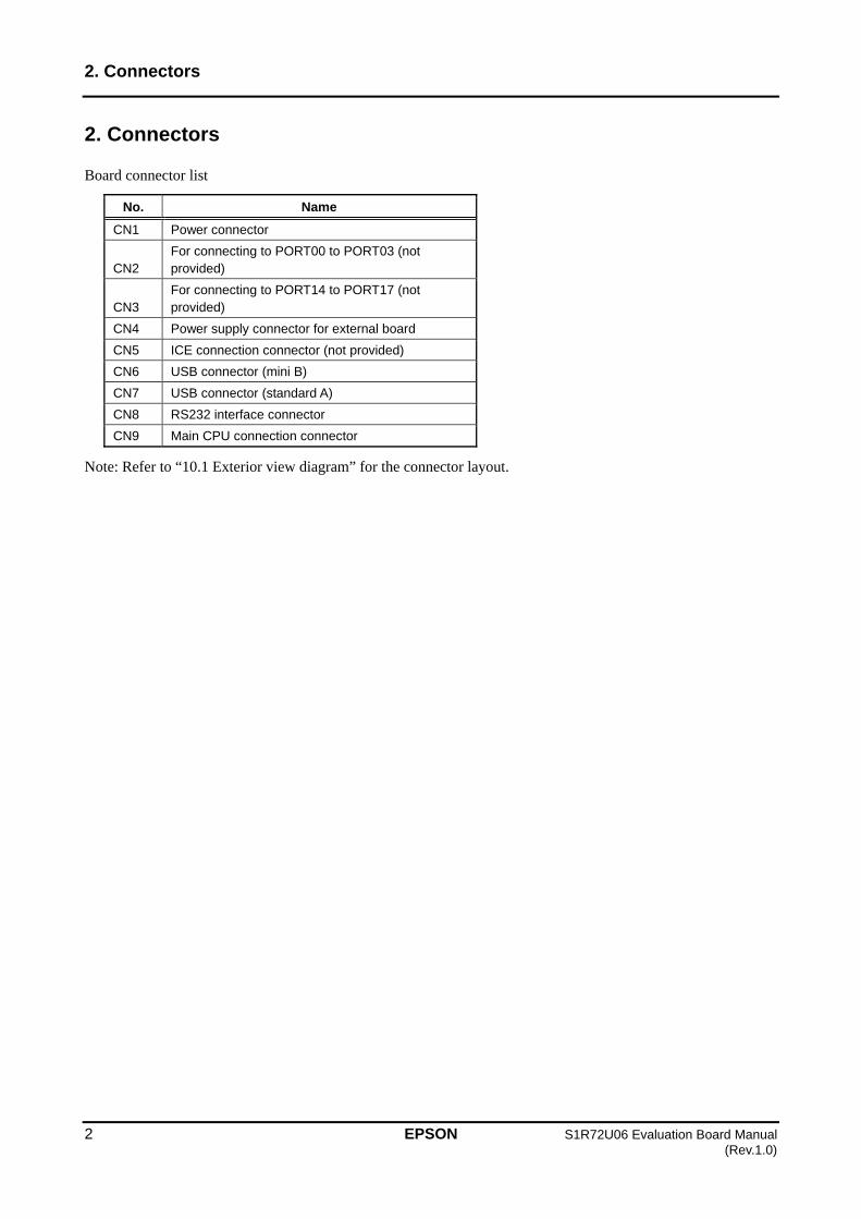
2. Connectors
2 EPSON S1R72U06 Evaluation Board Manual (Rev.1.0)
2. Connectors
Board connector list
No. Name
CN1 Power connector
CN2 For connecting to PORT00 to PORT03 (not provided)
CN3 For connecting to PORT14 to PORT17 (not provided)
CN4 Power supply connector for external board
CN5 ICE connection connector (not provided)
CN6 USB connector (mini B)
CN7 USB connector (standard A)
CN8 RS232 interface connector
CN9 Main CPU connection connector
Note: Refer to “10.1 Exterior view diagram” for the connector layout.
3. Jumper Settings
S1R72U06 Evaluation Board Manual EPSON 3 (Rev.1.0)
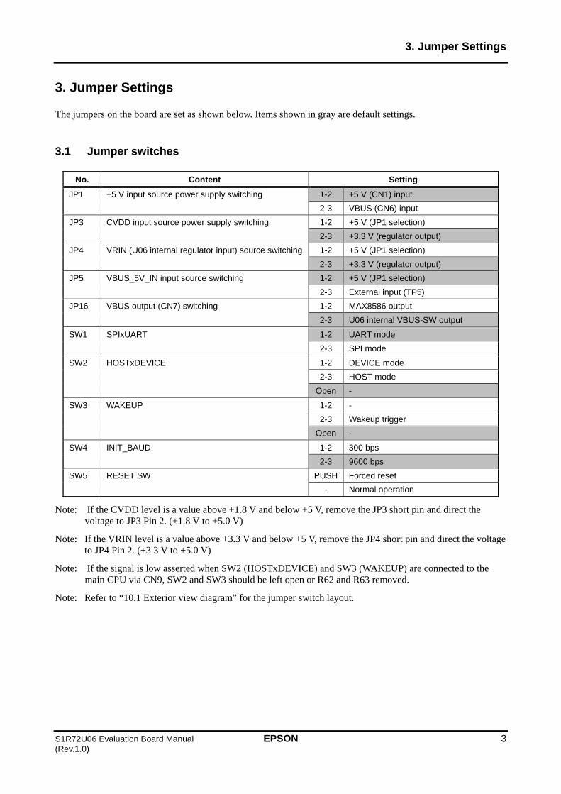
3. Jumper Settings
The jumpers on the board are set as shown below. Items shown in gray are default settings.
3.1 Jumper switches
No. Content Setting
JP1 +5 V input source power supply switching 1-2 +5 V (CN1) input
2-3 VBUS (CN6) input
JP3 CVDD input source power supply switching 1-2 +5 V (JP1 selection)
2-3 +3.3 V (regulator output)
JP4 VRIN (U06 internal regulator input) source switching 1-2 +5 V (JP1 selection)
2-3 +3.3 V (regulator output)
JP5 VBUS_5V_IN input source switching 1-2 +5 V (JP1 selection)
2-3 External input (TP5)
JP16 VBUS output (CN7) switching 1-2 MAX8586 output
2-3 U06 internal VBUS-SW output
SW1 SPIxUART 1-2 UART mode
2-3 SPI mode
SW2 HOSTxDEVICE 1-2 DEVICE mode
2-3 HOST mode
Open -
SW3 WAKEUP 1-2 -
2-3 Wakeup trigger
Open -
SW4 INIT_BAUD 1-2 300 bps
2-3 9600 bps
SW5 RESET SW PUSH Forced reset
- Normal operation
Note: If the CVDD level is a value above +1.8 V and below +5 V, remove the JP3 short pin and direct the voltage to JP3 Pin 2. (+1.8 V to +5.0 V)
Note: If the VRIN level is a value above +3.3 V and below +5 V, remove the JP4 short pin and direct the voltage to JP4 Pin 2. (+3.3 V to +5.0 V)
Note: If the signal is low asserted when SW2 (HOSTxDEVICE) and SW3 (WAKEUP) are connected to the main CPU via CN9, SW2 and SW3 should be left open or R62 and R63 removed.
Note: Refer to “10.1 Exterior view diagram” for the jumper switch layout.
3. Jumper Settings
4 EPSON S1R72U06 Evaluation Board Manual (Rev.1.0)
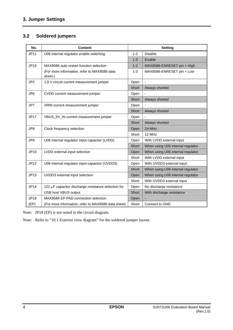
3.2 Soldered jumpers
No. Content Setting
JP11 U06 internal regulator enable switching 1-2 Disable
1-3 Enable
JP15 MAX8586 auto restart function selection 1-2 MAX8586-ENRESET pin = High
(For more information, refer to MAX8586 data sheet.)
1-3 MAX8586-ENRESET pin = Low
JP2 1.8 V circuit current measurement jumper Open -
Short Always shorted
JP6 CVDD current measurement jumper Open -
Short Always shorted
JP7 VRIN current measurement jumper Open -
Short Always shorted
JP17 VBUS_5V_IN current measurement jumper Open -
Short Always shorted
JP8 Clock frequency selection Open 24 MHz
Short 12 MHz
JP9 U06 internal regulator input capacitor (LVDD) Open With LVDD external input
Short When using U06 internal regulator
JP10 LVDD external input selection Open When using U06 internal regulator
Short With LVDD external input
JP12 U06 internal regulator input capacitor (UVDD3) Open With UVDD3 external input
Short When using U06 internal regulator
JP13 UVDD3 external input selection Open When using U06 internal regulator
Short With UVDD3 external input
JP14 122 F capacitor discharge resistance selection for Open No discharge resistance
USB host VBUS output Short With discharge resistance
JP18 MAX8586 EP-PAD connection selection Open -
(EP) (For more information, refer to MAX8586 data sheet) Short Connect to GND
Note: JP18 (EP) is not noted in the circuit diagram.
Note: Refer to “10.1 Exterior view diagram” for the soldered jumper layout.
4. LEDs
S1R72U06 Evaluation Board Manual EPSON 5 (Rev.1.0)
4. LEDs
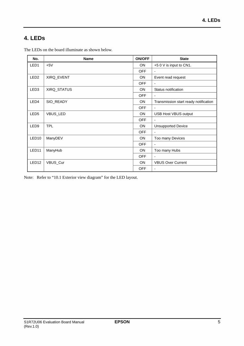
The LEDs on the board illuminate as shown below.
No. Name ON/OFF State
LED1 +5V ON +5 0 V is input to CN1.
OFF -
LED2 XIRQ_EVENT ON Event read request
OFF -
LED3 XIRQ_STATUS ON Status notification
OFF -
LED4 SIO_READY ON Transmission start ready notification
OFF -
LED5 VBUS_LED ON USB Host VBUS output
OFF -
LED9 TPL ON Unsupported Device
OFF -
LED10 ManyDEV ON Too many Devices
OFF -
LED11 ManyHub ON Too many Hubs
OFF -
LED12 VBUS_Cur ON VBUS Over Current
OFF -
Note: Refer to “10.1 Exterior view diagram” for the LED layout.
5. USB Interface Peripheral Circuit
6 EPSON S1R72U06 Evaluation Board Manual (Rev.1.0)
5. USB Interface Peripheral Circuit
This board includes the following two USB connectors:
CN6 (USB Mini B) for device functions CN7 (USB Standard A) for host functions
The DP and DM pins for these connectors are also connected to the DP and DM pins on S1R72U06 for evaluation convenience, but such circuits are not recommended. Mounting components or using wiring patterns like this may upset impedance matching and reduce signal quality, resulting in communication problems. For more information, refer to the S1R72V Series USB2.0 Hi-Speed PCB Design Guidelines.
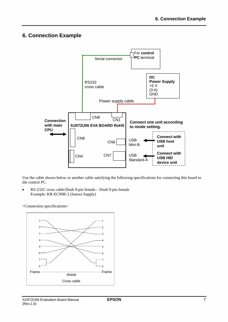
6. Connection Example
S1R72U06 Evaluation Board Manual EPSON 7 (Rev.1.0)
For control PC terminal Serial connector
RS232 cross cable
Power supply cable
CN8 CN1
CN6
CN7 CN4
CN9 USB Mini-B
USB Standard-A
DC Power Supply +5 V (3 A) GND
S1R72U06 EVA BOARD RoHS
Connect with USB host unit
Connect with USB HID device unit
Connect one unit according to mode setting.
Connection with main CPU
6. Connection Example
Use the cable shown below or another cable satisfying the following specifications for connecting this board to the control PC.
RS-232C cross cable/Dsub 9-pin female – Dsub 9-pin female Example: KR-EC99R-2 (Sanwa Supply)
<Connection specifications>
Cross cable
Shield Frame Frame
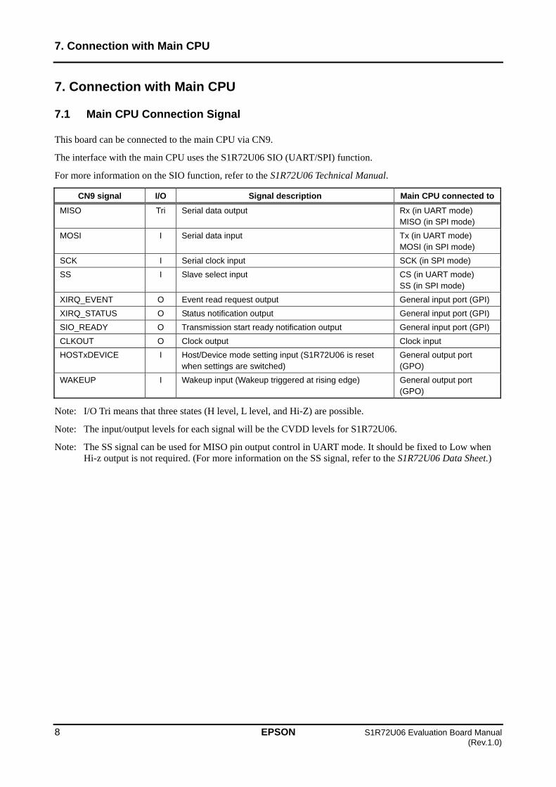
7. Connection with Main CPU
8 EPSON S1R72U06 Evaluation Board Manual (Rev.1.0)
7. Connection with Main CPU
7.1 Main CPU Connection Signal
This board can be connected to the main CPU via CN9.
The interface with the main CPU uses the S1R72U06 SIO (UART/SPI) function.
For more information on the SIO function, refer to the S1R72U06 Technical Manual.
CN9 signal I/O Signal description Main CPU connected to
MISO Tri Serial data output Rx (in UART mode) MISO (in SPI mode)
MOSI I Serial data input Tx (in UART mode) MOSI (in SPI mode)
SCK I Serial clock input SCK (in SPI mode)
SS I Slave select input CS (in UART mode) SS (in SPI mode)
XIRQ_EVENT O Event read request output General input port (GPI)
XIRQ_STATUS O Status notification output General input port (GPI)
SIO_READY O Transmission start ready notification output General input port (GPI)
CLKOUT O Clock output Clock input
HOSTxDEVICE I Host/Device mode setting input (S1R72U06 is reset when settings are switched)
General output port (GPO)
WAKEUP I Wakeup input (Wakeup triggered at rising edge) General output port (GPO)
Note: I/O Tri means that three states (H level, L level, and Hi-Z) are possible.
Note: The input/output levels for each signal will be the CVDD levels for S1R72U06.
Note: The SS signal can be used for MISO pin output control in UART mode. It should be fixed to Low when Hi-z output is not required. (For more information on the SS signal, refer to the S1R72U06 Data Sheet.)
7. Connection with Main CPU
S1R72U06 Evaluation Board Manual EPSON 9 (Rev.1.0)
CN9
SIO_READY
XIRQ_STATUS
XIRQ_EVENT
WAKEUP
MOSI
MISO Rx
Tx
GPO_0
GPI_0
GPI_1
GPI_2
S1R72U06 EVA BOARD RoHS Main CPU
CN9
SIO_READY
XIRQ_STATUS
XIRQ_EVENT
WAKEUP
SCK
MISO MISO
SCK
GPO_0
GPI_0
GPI_1
GPI_2
S1R72U06 EVA BOARD RoHSMain CPU
MOSI MOSI
SS SS
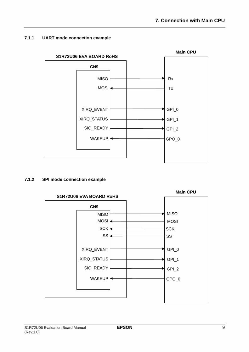
7.1.1 UART mode connection example
7.1.2 SPI mode connection example

7. Connection with Main CPU
10 EPSON S1R72U06 Evaluation Board Manual (Rev.1.0)
7.2 Connection cable example
This is a typical cable for connecting to CN9.
Connect the connector end to CN9. The main CPU end should be modified as required to suit the client’s configuration.
(L= desired length)
Flat cable AWG#28 lattice type
HIF3A-20D-2.54R (Hirose) or similar product

8. Power Supply
S1R72U06 Evaluation Board Manual EPSON 11 (Rev.1.0)
8. Power Supply
The power supply for this board should be supplied to CN1, as shown below.
1 pin +5 V
2 pin GND
3 pin N.C.
4 pin N.C.
Note: When inputting a different voltage to CVDD or VRIN, refer to “3. Jumper Settings.”
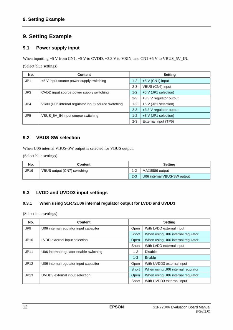
9. Setting Example
12 EPSON S1R72U06 Evaluation Board Manual (Rev.1.0)
9. Setting Example
9.1 Power supply input
When inputting +5 V from CN1, +5 V to CVDD, +3.3 V to VRIN, and CN1 +5 V to VBUS_5V_IN.
(Select blue settings)
No. Content Setting
JP1 +5 V input source power supply switching 1-2 +5 V (CN1) input
2-3 VBUS (CN6) input
JP3 CVDD input source power supply switching 1-2 +5 V (JP1 selection)
2-3 +3.3 V regulator output
JP4 VRIN (U06 internal regulator input) source switching 1-2 +5 V (JP1 selection)
2-3 +3.3 V regulator output
JP5 VBUS_5V_IN input source switching 1-2 +5 V (JP1 selection)
2-3 External input (TP5)
9.2 VBUS-SW selection
When U06 internal VBUS-SW output is selected for VBUS output.
(Select blue settings)
No. Content Setting
JP16 VBUS output (CN7) switching 1-2 MAX8586 output
2-3 U06 internal VBUS-SW output
9.3 LVDD and UVDD3 input settings
9.3.1 When using S1R72U06 internal regulator output for LVDD and UVDD3
(Select blue settings)
No. Content Setting
JP9 U06 internal regulator input capacitor Open With LVDD external input
Short When using U06 internal regulator
JP10 LVDD external input selection Open When using U06 internal regulator
Short With LVDD external input
JP11 U06 internal regulator enable switching 1-2 Disable
1-3 Enable
JP12 U06 internal regulator input capacitor Open With UVDD3 external input
Short When using U06 internal regulator
JP13 UVDD3 external input selection Open When using U06 internal regulator
Short With UVDD3 external input
9. Setting Example
S1R72U06 Evaluation Board Manual EPSON 13 (Rev.1.0)
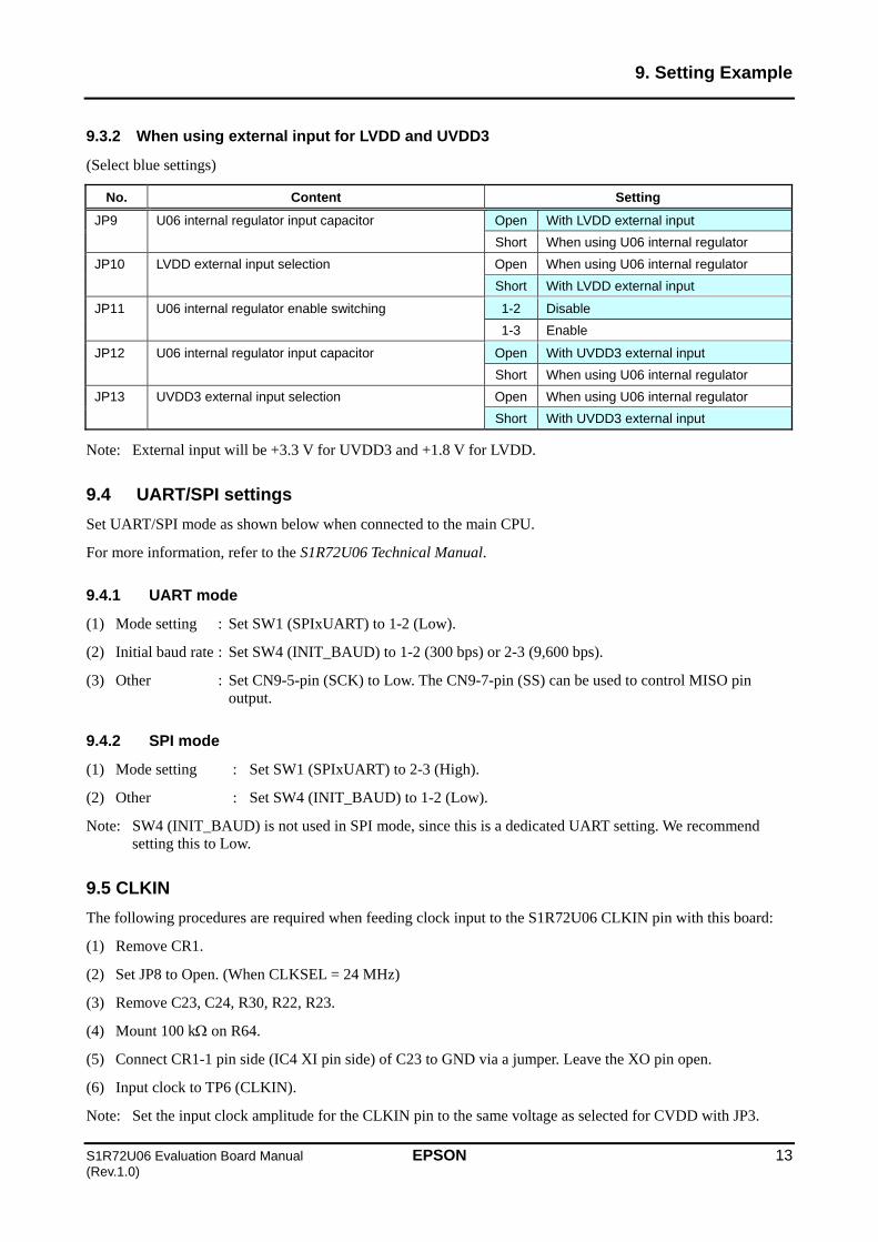
9.3.2 When using external input for LVDD and UVDD3
(Select blue settings)
No. Content Setting
JP9 U06 internal regulator input capacitor Open With LVDD external input
Short When using U06 internal regulator
JP10 LVDD external input selection Open When using U06 internal regulator
Short With LVDD external input
JP11 U06 internal regulator enable switching 1-2 Disable
1-3 Enable
JP12 U06 internal regulator input capacitor Open With UVDD3 external input
Short When using U06 internal regulator
JP13 UVDD3 external input selection Open When using U06 internal regulator
Short With UVDD3 external input
Note: External input will be +3.3 V for UVDD3 and +1.8 V for LVDD.
9.4 UART/SPI settings
Set UART/SPI mode as shown below when connected to the main CPU.
For more information, refer to the S1R72U06 Technical Manual.
9.4.1 UART mode
(1) Mode setting : Set SW1 (SPIxUART) to 1-2 (Low).
(2) Initial baud rate : Set SW4 (INIT_BAUD) to 1-2 (300 bps) or 2-3 (9,600 bps).
(3) Other : Set CN9-5-pin (SCK) to Low. The CN9-7-pin (SS) can be used to control MISO pin output.
9.4.2 SPI mode
(1) Mode setting : Set SW1 (SPIxUART) to 2-3 (High).
(2) Other : Set SW4 (INIT_BAUD) to 1-2 (Low).
Note: SW4 (INIT_BAUD) is not used in SPI mode, since this is a dedicated UART setting. We recommend setting this to Low.
9.5 CLKIN
The following procedures are required when feeding clock input to the S1R72U06 CLKIN pin with this board:
(1) Remove CR1.
(2) Set JP8 to Open. (When CLKSEL = 24 MHz)
(3) Remove C23, C24, R30, R22, R23.
(4) Mount 100 k on R64.
(5) Connect CR1-1 pin side (IC4 XI pin side) of C23 to GND via a jumper. Leave the XO pin open.
(6) Input clock to TP6 (CLKIN).
Note: Set the input clock amplitude for the CLKIN pin to the same voltage as selected for CVDD with JP3.

10. Appendix
14 EPSON S1R72U06 Evaluation Board Manual (Rev.1.0)
10. Appendix
10.1 Exterior view diagram
CN9: Main CPU connector
CN1: Power supply connector
CN7: USB Standard-A connector
CN6: USB Mini-B connector IC4:
S1R72U06
CN4: Power supply output connector
CN8: RS232 connector
SW1-SW4: Mode setting switches
LED2, 3, 4, 9, 10, 11, 12: Status LEDs
SW5: Reset switch
10. Appendix
S1R72U06 Evaluation Board Manual EPSON 15 (Rev.1.0)
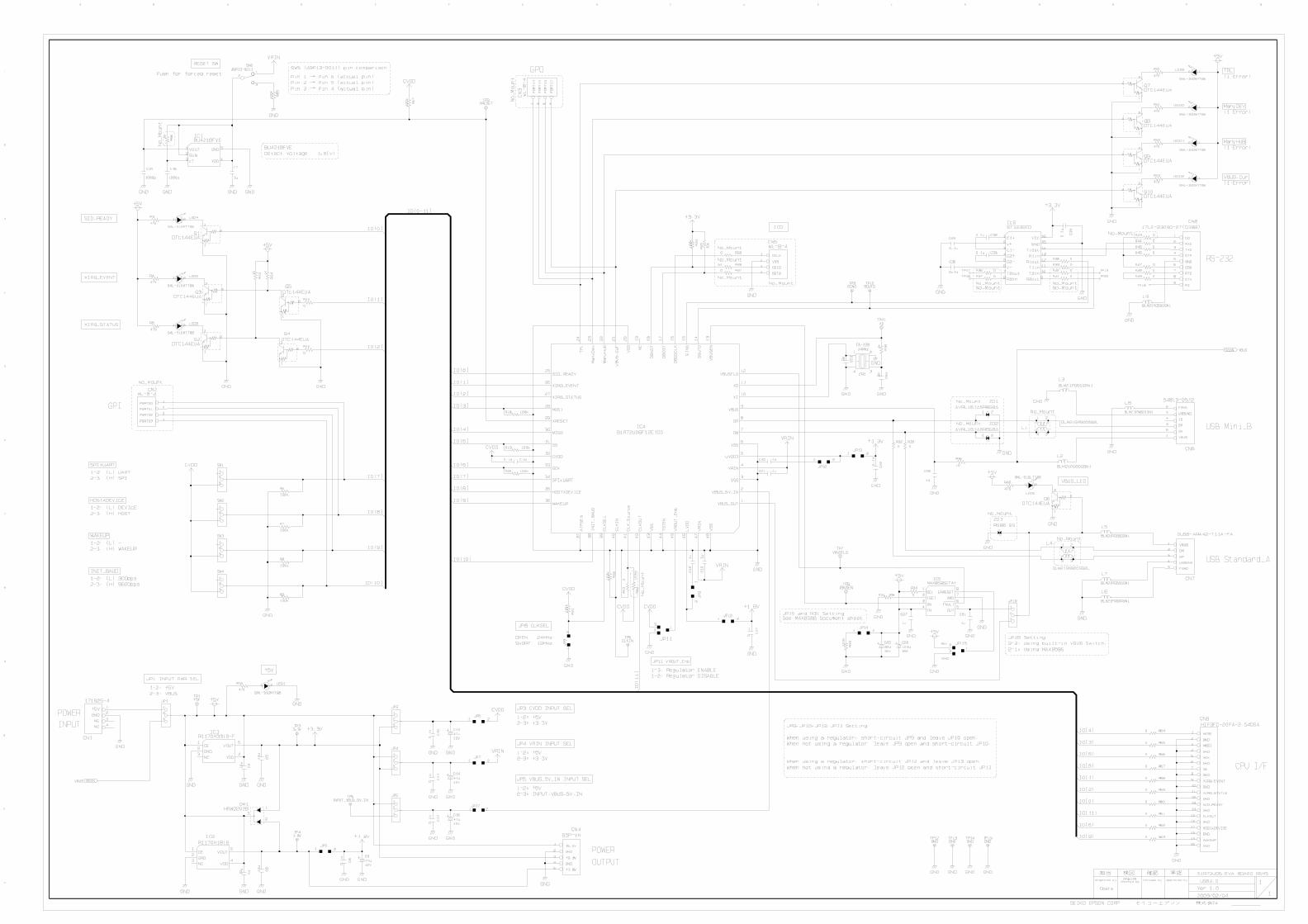
10.2 Circuit diagram
Refer to attachments.
10.3 Component list
Refer to attachments.
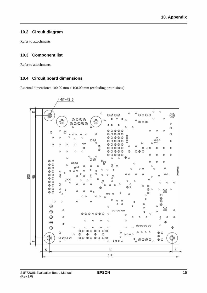
10.4 Circuit board dimensions
External dimensions: 100.00 mm x 100.00 mm (excluding protrusions)
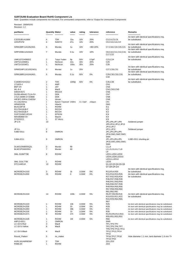
S1R72U06 Evaluation Board RoHS Component ListNote: Quantities include components not mounted. For unmounted components, refer to “Output for Unmounted Components
Revised: 2009/02/03Revision: 1.0
partName Quantity Maker value rating tolerance reference Remarks---------------------- ---------- ------------ ------- -------- ------------- ------------------ ------------------
C3225JB1A106M 4 TDK 10u 10V 20% C3,C4,C5,C6An item with identical specifications maybe substituted.
10SVP47M 4 SANYO 47u 10V 20% C9,C13,C14,C15
GRM188F11A105ZA01 5 Murata 1u 10V +80/-20% C7,C18,C19,C20,C21An item with identical specifications maybe substituted.
GRP155B11A104ZA 7 Murata 0.1u 10V 10% C8,C10,C11,C12,C16,An item with identical specifications maybe substituted.
C17,C22
UMK107CH090DZ 2 Taiyo Yuden 9p 50V 0.5pF C23,C24An item with identical specifications maybe substituted.
UWT1C220MCL 1 Nichicon 22u 16V 20% C25UWT1V101MCL 1 Nichicon 100u 35V 20% C26
GRM31MF11E105ZA01L 3 Murata 1u 25V C27,C28,C31An item with identical specifications maybe substituted.
GRM188R11H104JA01 5 Murata 0.1u 50V 5% C29,C30,C32,C33,An item with identical specifications maybe substituted.
C34
C1608CH1H102J 2 TDK 1000p 50V 5% C35,C36An item with identical specifications maybe substituted.
171825-4 1 AMP CN1B5P-VH 1 JST CN4WL-8-4 3 Mac8 CN2,CN3,CN554819-0572 1 MOLEX CN6DUSB-ARA42-T11A-FA 1 DDK CN717LE-23090-27(D3BB) 1 DDK CN8HIF3FC-20PA-2.54DSA 1 Hirose CN9FA-128(24MHz) 1 Epson Toyocom 24MHz CL=10pF ±50ppm CR1HRW0202B 1 Hitachi DM1BU4218FVE 1 ROHM IC1R1170H181B-F 1 RICOH IC2R1170H331B-F 1 RICOH IC3S1R72U06F12E100 1 EPSON IC4MAX8586ETA+ 1 Maxim IC5ST3232CD 1 ST Micro IC6JP-2-A 10 JP2,JP6,JP7,JP8, Soldered jumper
JP9,JP10,JP12,JP13JP14,JP17
JP-3-L 2 JP11,JP15 Soldered jumperXJ8D-0311 9 OMRON JP1,JP3,JP4,JP5,
JP16,SW1,SW2,SW3,SW4
XJ8A-0211 9 OMRON JP1,JP3,JP4,JP5, XJ8D-0311 shorting pinJP16,SW1,SW2,SW3,SW4
DLW21SN900SQ2L 2 Murata 90 L1,L4BLM21PG600SN1 7 Murata 60 L2,L3,L5,L6,L7,L8
L9SML-310MTT86 8 ROHM LED1,LED2,LED3,
LED4,LED9,LED10,LED11,LED12
SML-310LTT86 1 ROHM LED5DTC144EUA 10 ROHM Q1,Q2,Q3,Q4,Q5,Q6
Q7,Q8,Q9,Q10
MCR03EZHJ102 3 ROHM 1k 1/16W 5% R13,R14,R30An item with identical specifications maybe substituted.
MCR03EZHJ000 31 ROHM 0 1/16W 5% R15,R16,R23,R26, An item with identical specifications mayR27,R32,R33,R34, be substituted.R36,R37,R38,R39,R40,R41,R43,R44,R45,R46,R47,R48,R49,R54,R55,R56,R57,R58,R59,R60,R61,R62,R63
MCR03EZHJ104 14 ROHM 100k 1/16W 5% R6,R7,R8,R9,R18, An item with identical specifications mayR19,R20,R21,R22, be substituted.R24,R29,R64,R65,R67
MCR03EZHJ103 1 ROHM 10k 1/16W 5% R25 An item with identical specifications may be substituted.MCR03EZHJ330 1 ROHM 33 1/16W 5% R28 An item with identical specifications may be substituted.MCR03EZHJ393 1 ROHM 39k 1/16W 5% R31 An item with identical specifications may be substituted.MCR03EZHJ100 1 ROHM 10 1/16W 5% R35 An item with identical specifications may be substituted.MCR03EZHJ471 9 ROHM 470 1/16W 5% R3,R4,R5,R12,R42, An item with identical specifications may be substituted.
R50,R51,R52,R53MCR03EZHJ105 1 ROHM 1M 1/16W 5% R66 An item with identical specifications may be substituted.A9P13-0011 1 OMRON SW5LC-33-S-Red 3 Mac8 TP1,TP3,TP4LC-33-S-Yellow 8 Mac8 TP2,TP5,TP6,TP7,
TP8,TP9,TP10,TP11LC-33-S-Black 4 Mac8 TP12,TP13,TP14,
TP15Round_Pattern 5 no_maker TP16,TP17,TP18, Hole diameter 1.1 mm, land diameter 1.6 mm TH
TP19,TP20AVRL161A6R8GBA 2 TDK ZD1,ZD2RSB6.8S 1 ROHM ZD3
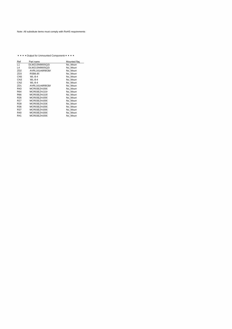
Note: All substitute items must comply with RoHS requirements
****Output for Unmounted Components****
Ref Part name Mounted flagL1 DLW21SN900SQ2L No_MountL4 DLW21SN900SQ2L No_MountZD2 AVRL161A6R8GBA No_MountZD3 RSB6.8S No_MountCN5 WL-8-4 No_MountCN3 WL-8-4 No_MountCN2 WL-8-4 No_MountZD1 AVRL161A6R8GBA No_MountR43 MCR03EZHJ000 No_MountR64 MCR03EZHJ104 No_MountR66 MCR03EZHJ105 No_MountR26 MCR03EZHJ000 No_MountR27 MCR03EZHJ000 No_MountR28 MCR03EZHJ330 No_MountR36 MCR03EZHJ000 No_MountR37 MCR03EZHJ000 No_MountR40 MCR03EZHJ000 No_MountR41 MCR03EZHJ000 No_Mount
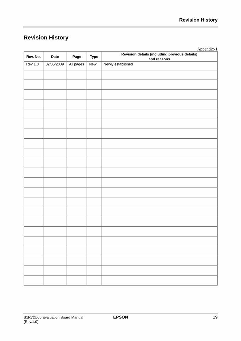
Revision History
S1R72U06 Evaluation Board Manual EPSON 19 (Rev.1.0)
Revision History
Appendix-1
Rev. No. Date Page Type Revision details (including previous details)
and reasons Rev 1.0 02/05/2009 All pages New Newly established
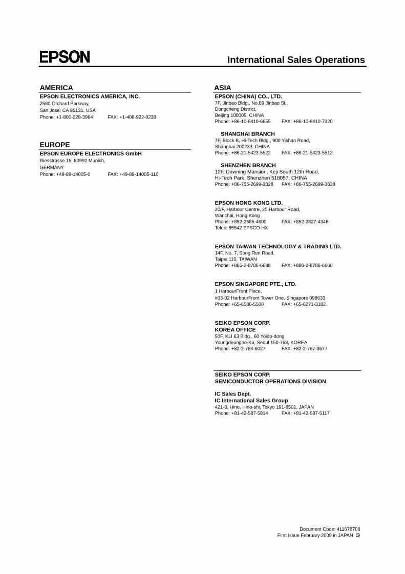
International Sales Operations
AMERICA EPSON ELECTRONICS AMERICA, INC. 2580 Orchard Parkway,
San Jose, CA 95131, USA
Phone: +1-800-228-3964 FAX: +1-408-922-0238
EUROPE EPSON EUROPE ELECTRONICS GmbH Riesstrasse 15, 80992 Munich,
GERMANY
Phone: +49-89-14005-0 FAX: +49-89-14005-110
ASIA EPSON (CHINA) CO., LTD. 7F, Jinbao Bldg., No.89 Jinbao St., Dongcheng District, Beijing 100005, CHINA Phone: +86-10-6410-6655 FAX: +86-10-6410-7320
SHANGHAI BRANCH 7F, Block B, Hi-Tech Bldg., 900 Yishan Road, Shanghai 200233, CHINA Phone: +86-21-5423-5522 FAX: +86-21-5423-5512
SHENZHEN BRANCH 12F, Dawning Mansion, Keji South 12th Road, Hi-Tech Park, Shenzhen 518057, CHINA Phone: +86-755-2699-3828 FAX: +86-755-2699-3838 EPSON HONG KONG LTD. 20/F, Harbour Centre, 25 Harbour Road, Wanchai, Hong Kong Phone: +852-2585-4600 FAX: +852-2827-4346 Telex: 65542 EPSCO HX EPSON TAIWAN TECHNOLOGY & TRADING LTD. 14F, No. 7, Song Ren Road, Taipei 110, TAIWAN Phone: +886-2-8786-6688 FAX: +886-2-8786-6660 EPSON SINGAPORE PTE., LTD. 1 HarbourFront Place,
#03-02 HarbourFront Tower One, Singapore 098633 Phone: +65-6586-5500 FAX: +65-6271-3182 SEIKO EPSON CORP. KOREA OFFICE 50F, KLI 63 Bldg., 60 Yoido-dong, Youngdeungpo-Ku, Seoul 150-763, KOREA Phone: +82-2-784-6027 FAX: +82-2-767-3677
SEIKO EPSON CORP. SEMICONDUCTOR OPERATIONS DIVISION IC Sales Dept. IC International Sales Group 421-8, Hino, Hino-shi, Tokyo 191-8501, JAPAN Phone: +81-42-587-5814 FAX: +81-42-587-5117
Document Code: 411678700 First Issue February 2009 in JAPAN ○D