Embed Size (px)
Citation preview

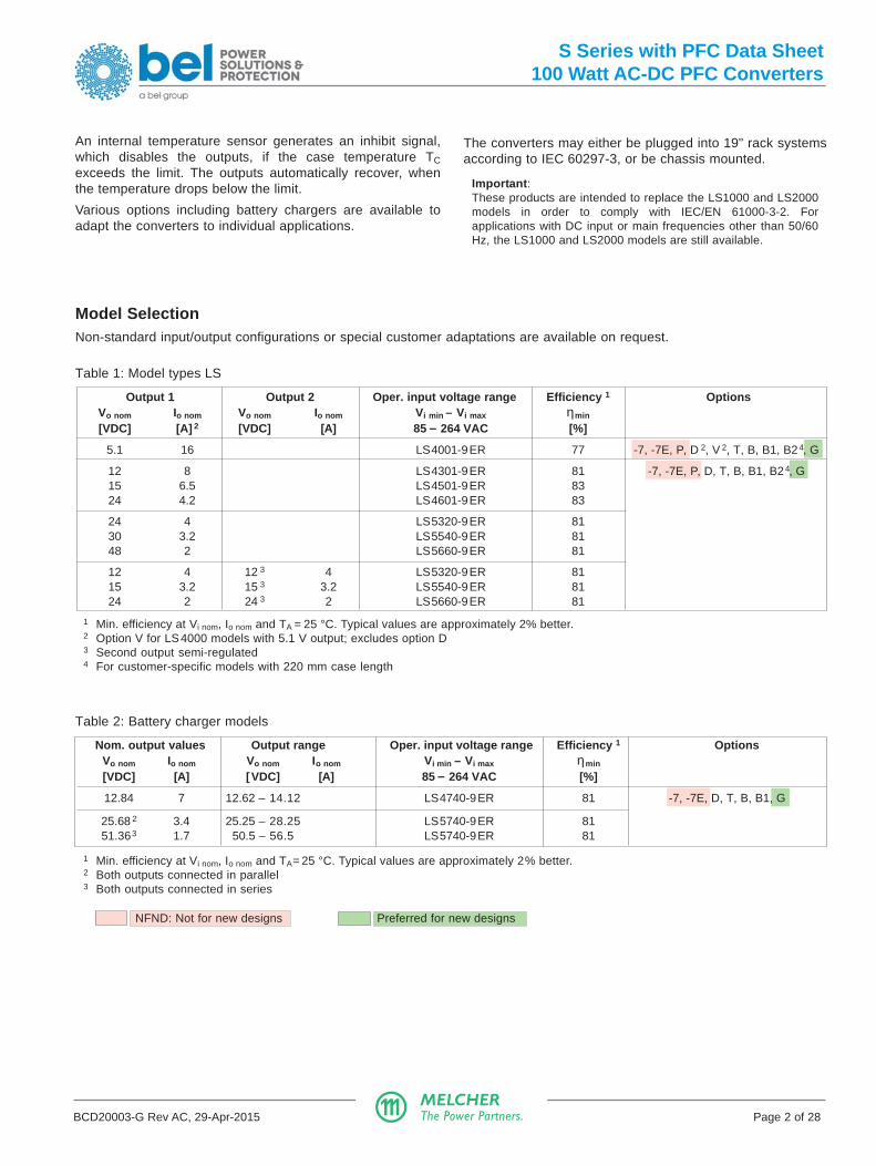
S Series with PFC Data Sheet100 Watt AC-DC PFC Converters
BCD20003-G Rev AC, 29-Apr-2015 Page 1 of 28MELCHERThe Power Partners.
DescriptionThe LS 4000/5000 Series of AC-DC converters represents aflexible range of power supplies for use in advancedelectronic systems. Features include full power factorcorrection, good hold-up time, high efficiency and reliability,low output voltage noise, and excellent dynamic response toload/line changes.
The converters are protected against surges and transientsoccurring at the source lines. Input over- and undervoltagelockout circuitry disables the outputs, when the input voltageis outside of the specified range. Input inrush current limitationis included for preventing circuit breakers and fuses fromtripping at switch-on.
All outputs are overload, open- and short-circuit proof andprotected by a built-in suppressor diode. The outputs can be
inhibited by a logic signal applied to connector pin 18. If theinhibit function is not used, pin 18 must be connected with pin14 to enable the outputs.
LED indicators display the status of the converter and allowvisual monitoring of the system at any time.
Full input to output, input to case, output to case and output tooutput isolation is provided. The converters are designed andbuilt according to the international safety standards IEC/EN60950-1 2nd
The case design allows operation at nominal load up to 71 °Cin a free air ambient temperature. If forced cooling is provided,the ambient temperature may exceed 71 °C but the casetemperature must remain below 95 °C under all conditions.
1686.6"
602.4"12 TE
1114.4"3 U
Features• RoHS lead-free-solder and lead-solder-exempted pro-
ducts are available.
• Class I equipment
• Power factor >0.93, harmonics IEC/EN 61000-3-2• Immunity according to IEC/EN 61000-4-2, -3, -4, -5,
-6, -8, -9• Compliant with EN 50155, EN 50121-4, EN 45545.
• High efficiency• Input over- and undervoltage lockout
• Adjustable output voltage with remote on/off
• 1 or 2 outputs: SELV, no load, overload, and short-circuitproof
• Rectangular current limiting characteristic
• PCBs protected by lacquer
• Very high reliability
Safety-approved according to IEC/EN 60950-1, UL/CSA60950-1 2nd Ed.
Table of Contents Page Page
Copyright © 2015, Bel Power Solutions Inc. All rights reserved.
Description ....................................................................... 1Model Selection ............................................................... 2Functional Description ..................................................... 4Electrical Input Data ........................................................ 5Electrical Output Data ..................................................... 7Auxiliary Functions ........................................................ 11
Electromagnetic Compatibility (EMC) ........................... 15Environmental Conditions ............................................. 16Mechanical Data ............................................................ 17Safety and Installation Instructions ............................... 19Description of Options ................................................... 21Accessories ................................................................... 27
Ed. They have been approved by the safetyagencies Nemko and CSA (for USA and Canada).
S Series with PFC Data Sheet100 Watt AC-DC PFC Converters
BCD20003-G Rev AC, 29-Apr-2015 Page 2 of 28MELCHERThe Power Partners.
An internal temperature sensor generates an inhibit signal,which disables the outputs, if the case temperature TC
exceeds the limit. The outputs automatically recover, whenthe temperature drops below the limit.
Various options including battery chargers are available toadapt the converters to individual applications.
Model SelectionNon-standard input/output configurations or special customer adaptations are available on request.
The converters may either be plugged into 19" rack systemsaccording to IEC 60297-3, or be chassis mounted.
Important:These products are intended to replace the LS1000 and LS2000models in order to comply with IEC/EN 61000-3-2. Forapplications with DC input or main frequencies other than 50/60Hz, the LS1000 and LS2000 models are still available.
Table 1: Model types LS
Output 1 Output 2 Oper. input voltage range Efficiency 1 OptionsVo nom Io nom Vo nom Io nom Vi min – Vi max ηmin
[VDC] [A] 2 [VDC] [A] 85 – 264 VAC [%]
5.1 16 LS4001-9ER 77 -7, -7E, P, D 2, V 2, T, B, B1, B2 4, G
12 8 LS4301-9ER 81 -7, -7E, P, D, T, B, B1, B2 4, G15 6.5 LS4501-9ER 8324 4.2 LS4601-9ER 83
24 4 LS5320-9ER 8130 3.2 LS5540-9ER 8148 2 LS5660-9ER 81
12 4 12 3 4 LS5320-9ER 8115 3.2 15 3 3.2 LS5540-9ER 8124 2 24 3 2 LS5660-9ER 81
1 Min. efficiency at Vi nom, Io nom and TA = 25 °C. Typical values are approximately 2% better.2 Option V for LS4000 models with 5.1 V output; excludes option D3 Second output semi-regulated4 For customer-specific models with 220 mm case length
Table 2: Battery charger models
Nom. output values Output range Oper. input voltage range Efficiency 1 OptionsVo nom Io nom Vo nom Io nom Vi min – Vi max ηmin
[VDC] [A] [VDC] [A] 85 – 264 VAC [%]
12.84 7 12.62 – 14.12 LS4740-9ER 81 -7, -7E, D, T, B, B1, G
25.68 2 3.4 25.25 – 28.25 LS5740-9ER 8151.36 3 1.7 50.5 – 56.5 LS5740-9ER 81
1 Min. efficiency at Vi nom, Io nom and TA= 25 °C. Typical values are approximately 2% better.2 Both outputs connected in parallel3 Both outputs connected in series
NFND: Not for new designs Preferred for new designs

S Series with PFC Data Sheet100 Watt AC-DC PFC Converters
BCD20003-G Rev AC, 29-Apr-2015 Page 3 of 28MELCHERThe Power Partners.
Example: LS5540-9ERD3TB1G: Power factor corrected AC-DC converter, operating input voltage range 85 – 264 VAC,2 electrically isolated outputs, each providing 15 V, 3.2 A, equipped with inrush current limiter, R-input to adjust theoutput voltages, undervoltage monitor D3, current share feature, a cooling plate B1, RoHS-compatibel.
Product MarkingBasic type designation, applicable approval marks, CE mark,warnings, pin designation, Power-One patents and companylogo, identification of LEDs, test sockets, and potentiometer.
Specific type designation, input voltage range, nominal outputvoltages and currents, degree of protection, batch no., serialno., and data code including production site, modificationstatus and date of production.
Part Number Description
Operating input voltage Vi: 85 – 264 VAC ....................... LS
Number of outputs ....................................................... 4, 5
Single output models:Nominal voltage output 1 (main output), Vo1 nom
5.1 V ..................................................................... 0, 1, 212 V .............................................................................. 315 V .......................................................................... 4, 524 V .............................................................................. 6Other voltages 1 ....................................................... 7, 8Other specifications (single output models)1 ....... 01 – 99
Double output models:
Nominal voltage output 1 and 212 V, 12 V ............................................................................................... 2015 V, 15 V ............................................................................................... 4024 V, 24 V .................................................................. 60Other specifications or additional features 1 ....... 21– 99
Operational ambient temperature range TA:–25 to 71 °C ................................................................ -7–40 to 71 °C ................................................................ -9Other 1 ............................................................... -0, -5, -6
Auxiliary functions and options:Inrush current limitation ............................................. E 2
Output voltage control input .......................................R 3
Potentiometer (output voltage adjustment) ................ P 3
Undervoltage monitor (D0 – DD, to be specified) ......D 4
ACFAIL signal (V2, V3, to be specified) .................... V 4
Current share ............................................................... TCooling plate standard case .............................. B or B1Cooling plate for long case 220 mm 1 ........................ B2RoHS-compliant for all 6 substances ..........................G
1 Customer-specific models2 Option E mandatory for all -9 models3 Feature R excludes option P and vice versa.4 Option D excludes option V and vice versa; option V is available for 5.1 V models only.
Note: The sequence of options must follow the order above. This part number description is descriptive only; it is not inteded forcreating part numbers.
LS 5 5 40 -9 E R D3 T B1 G
NFND: Not for new designs Preferred for new designs

S Series with PFC Data Sheet100 Watt AC-DC PFC Converters
BCD20003-G Rev AC, 29-Apr-2015 Page 4 of 28MELCHERThe Power Partners.
Fig. 2Block diagram of double-output models
1 Transient suppressor (VDR)2 Inrush current limiter (NTC, only models with TA min = –25 °C ) or option E3 Bulk capacitor Cb; bulk voltage approx. 370 V
Functional DescriptionThe input voltage is fed via an input fuse, an input filter, arectifier, and an inrush current limiter to a boost converter.This step-up converter provides a sinusoidal input current(IEC/EN 61000-3-2, class D equipment) and charges the bulkcapacitor C i to approx. 370 VDC. This capacitor sources asingle transistor forward converter and provides the powerduring the hold-up time.
Each output is powered by a separate secondary winding ofthe main transformer. The resultant voltages are rectified and
their ripple smoothed by a power choke and an output filter.The control logic senses the main output voltage Vo1 andgenerates, with respect to the maximum admissible outputcurrents, the control signal for the switching transistor of theforward converter.
The second output of double output models is tracking to themain output, but has its own current limiting circuit. If the mainoutput voltage drops due to current limitation, the secondoutput voltage will fall as well and vice versa.
Fig. 1Block diagram of single-output models
1 Transient suppressor (VDR)2 Inrush current limiter (NTC, only models with TA min = –25 °C ) or option E3 Bulk capacitor Cb; bulk voltage approx. 370 V
Input filter
Contr
ol circuit
P
2
16
18
20
22
12
4
6
8
10
14
Outp
ut
filter
28
3032
24
– +
Forw
ard
convert
er
(appro
x. 80 k
Hz)
+
Boost convert
er
(appro
x. 100 k
Hz)
Ci 3
03001c
R
i
D/V
T
S+
Vo+
Vo–
S–
26N~
L~
1
Bridge r
etifier
Fuse
CY
CY
CY
CY
Co
ntr
ol circu
it
P
16
18
20
22
12
14
4
6
8
10
Ou
tpu
t 2
filte
r
Ou
tpu
t 1
filte
r
26
28
3032
24
– +
03002c
N~
L~
R
i
D
T
Vo1+
Vo1–
Vo2+
Vo2–
CY
Inp
ut
filte
r
1
Brid
ge
re
tifie
r
CY
CY
Fu
se
Fo
rwa
rd c
on
ve
rte
r (a
pp
rox.
80
kH
z)
+
Bo
ost
co
nve
rte
r (a
pp
rox.
10
0 k
Hz)
Ci 3
2
S Series with PFC Data Sheet100 Watt AC-DC PFC Converters
BCD20003-G Rev AC, 29-Apr-2015 Page 5 of 28MELCHERThe Power Partners.
Electrical Input DataGeneral Conditions– TA = 25 °C, unless TC is specified.– Pin 18 connected to pin 14, R input not connected, Vo adjusted to Vo nom (option P)– Sense line pins S+ and S– connected to Vo+ and Vo–, respectively.
Table 3: Input data
Input LS Unit
Characteristics Conditions min typ max
Vi Rated input voltage range Io = 0 – Io nom 100 240 VAC 1
Vi op Operating input voltage range TC min – TC max 85 264
Vi nom Nominal input voltage 50 – 60 Hz 230
I i Input current Vi nom, Io nom 2 0.55 A
P i0 No-load input power Vi min – Vi max, Io = 0 7.5 9 W
P i inh Idle input power conv. inhibited 2 3
R i Input resistance 480 mΩ
RNTC NTC resistance (see fig. 3)3 conv. not operating 3200 4000
C i Input capacitance 80 100 120 µF
Vi RFI Conducted input RFI EN 55022 B
Radiated input RFI Vi nom, Io nom B
Vi abs Input voltage limits 283 VACwithout damage –400 400 VDC 4
1 Nominal frequency range: 50 – 60 Hz, operating frequency range 47 – 63 Hz2 With double-output models, both outputs loaded with Io nom3 Valid for -7 versions without option E. This is the NTC resistance value at 25 °C and applies to cold converters. Subsequent switch-on/
off cycles increase the inrush current peak value.4 Operation with DC input voltage is not specified and not recommended.
Input Transient ProtectionA VDR together with the input fuse and a symmetrical inputfilter form an effective protection against high input transientvoltages.
Input FuseA fuse mounted inside the converter in series to the phase lineprotects against severe defects. A second fuse in the neutralline may be necessary in certain applications; see InstallationInstructions.
Fuse specification:
Slow-blow, 4 A, 250 V, 5 × 20 mm.
Input Under- /Overvoltage LockoutIf the input voltage remains below approx. 65 VAC or exceedsVi abs, an internally generated inhibit signal disables theoutput(s). Do not check the overvoltage lockout function!
If Vi is below Vi min, but above the undervoltage lockout level,the output voltage may be below the value specified in thetables Electrical Output Data.
Inrush Current LimitationThe -7 models without option E incorporate an NTC resistor inthe input circuitry, which at initial turn-on reduces the peak
inrush current value by a factor of 5 to 10 to protectconnectors and switching devices from damage. Subsequentswitch-on cycles within short periods will cause an increase ofthe peak inrush current value due to the warming-up of theNTC resistor.
The inrush current peak value (initial switch-on cycle) can bedetermined by following calculation:
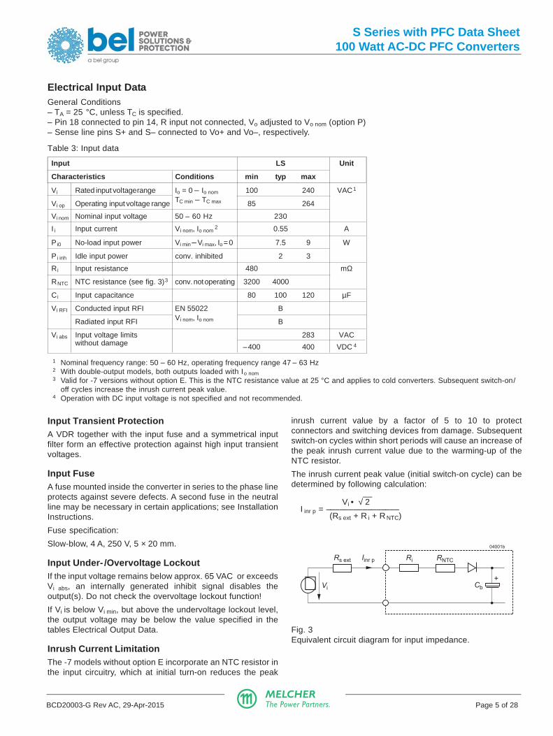
Vi • √ 2––
I inr p = –––––––––––––––– (Rs ext + R i + R NTC)
Fig. 3Equivalent circuit diagram for input impedance.
Rs ext Ri RNTCIinr p
Vi Cb
04001b
∼ +

S Series with PFC Data Sheet100 Watt AC-DC PFC Converters
BCD20003-G Rev AC, 29-Apr-2015 Page 6 of 28MELCHERThe Power Partners.
100 150 200 250 30050
1
3
0.5
1.5
2
2.5
li [A]
Vi [V]
04005a
Fig. 4Theoretical input inrush current versus time at Vi = 255 Vand 115 V, Rext = 0 for models without option E
Fig. 5Input current versus input voltage at Io nom
Fig. 7Harmonic currents at the input (LS4601, Vi = 230 VAC,Io = Io nom).
Power Factor and HarmonicsPower factor correction is achieved by controlling the inputcurrent waveform synchronously with the input voltagewaveform. The power factor control is active under alloperating conditions.
The harmonic distortion is well below the limits specified inIEC/EN 61000-3-2, class D.
Fig. 6Power factor versus output current (LS4601-7R)
Fig. 8Typ switching frequency versus load. The boostconverter at the input stage operates with a constantswitching frequency of 100 kHz.
Hold-up Time
Fig. 9
Hold-up time versus output power (LS4601-7R)
0
0.5
1
1.5
2
2.5
3
3.5
4
3 5 7 9 11 13
Harm-LS4601mA/W
Harm.
0.1 1 ms
50
100
Iinr [A]
0
04054LS
0.5
LS
0.2 0.4 0.6 0.8 10
60
0
10
20
30
40
50
kHz
Io/Io nom
70
80
1.2
05008b
020406080
100120140160180
0 0.2 0.4 0.6 0.8 Io/Io nom
[ms] LS4601-hu
Vi = 230 VAC
Vi = 85 VAC
0.70
0.75
0.80
0.85
0.90
0.95
1
0 0.2 0.4 0.6 0.8 1 Io/Io nom
Power factor
V i = 230 VAC
V i = 85 VAC
PF-LS4601

S Series with PFC Data Sheet100 Watt AC-DC PFC Converters
BCD20003-G Rev AC, 29-Apr-2015 Page 7 of 28MELCHERThe Power Partners.
Electrical Output DataGeneral Conditions:– TA = 25 °C, unless TC is specified.– Pin 18 (i) connected to pin 14 (S– or Vo1–), R input not connected, Vo adjusted to Vo nom (option P),– Sense line pins 12 (S+) and 14 (S–) connected to pins 4 (Vo1+) and 8 (Vo1–), respectively.
Table 4a: Output data of single-output models
LS4001 LS4301 / 4740 5 LS4501 LS4601 UnitOutput 5.1 V 12 V 5 15 V 24 V
Characteristics Conditions min typ max min typ max min typ max min typ max
Vo Output voltage Vi nom, Io nom 5.07 5.13 11.935 12.075 14.91 15.09 23.86 24.14 V
Vo BR Overvoltage protection 7.6 15.2 /17 5 19.6 28.5(supressor diode) 6
Io nom Output current nom. 1 Vi min – Vi max 16 8 /7 5 6.5 4.2 ATC min – TC max
IoL Output current limit 1 Vi min – Vi max 16.2 8.2/8 5 6.7 4.4
vo Output Low frequency Vi nom, Io nom 2 2 2 2 mVpp
noise 3Switching frequ. BW = 20 MHz 10 5 5 5
Total incl. spikes 50 40 40 40
∆Vo u Static line regulation Vi min – Vi max ±5 ±12 ±15 ±24 mVwith respect to Vi nom Io nom
∆Vo I Static load regulation Vi nom –20 –25 –30 –40(0.1 – 1) Io nom
vo d Dynamic Voltage Vi nom ±100 ±100 ±100 ±100load deviation 2 Io nom ↔ 1/2 Io nom
t dregulat. 2 Recovery time2 0.3 0.4 0.4 0.3 ms
α v o Temperature coefficient TC min – TCmax ±0.02 ±0.02 ±0.02 ±0.02 %/Kof output voltage 4 Io nom
1 If the output voltages are increased above Vo nom through R-input control, option P setting, remote sensing or option T, the outputcurrents should be reduced accordingly so that Po nom is not exceeded.
2 See Dynamic load regulation (fig. 13)3 Measured according to IEC/EN 61204 with a probe according to annex A4 For battery charger applications, a defined negative temperature coefficient can be provided by using a temperature sensor (see
Accessories), but we recommend choosing special battery charger models.5 Especially designed for battery charging using the temperature sensor (see Accessories). Vo is set to 12.84 V ±1% (R-input open).6 Breakdown voltage of the incorporated suppressor diode (1 mA; 10 mA for 5 V output). Exceeding Vo BR is dangerous for the
suppressor diode.
Fig. 10
Efficiency versus output power.
Efficiency
0.2 0.4 0.6 0.8 10
0.9
0.3
0.4
0.5
0.6
0.7
0.8
Efficiency
Io/Io nom
Vi = 230 V Vi = 85 V
05014a

S Series with PFC Data Sheet100 Watt AC-DC PFC Converters
BCD20003-G Rev AC, 29-Apr-2015 Page 8 of 28MELCHERThe Power Partners.
Table 4b: Output data of double-output models
LS5320 LS5540 UnitOutput 2 × 12 V 2 × 15 V
Characteristics Conditions Output 1 Output 2 Output 1 Output 2
min typ max min typ max min typ max min typ max
Vo Output voltage Vi nom, Io nom 1 11.93 12.07 11.82 12.18 14.91 15.09 14.78 15.22 V
Vo P Overvoltage protection 15.2 15.2 19.6 19.6(supressor diode) 8
Io nom Output current nom 2 Vi min – Vi max 4 4 3.2 3.2 ATC min – TC max
IoL Output current limit 6 Vi min – Vi max 4.2 4.2 3.4 3.4
uvo Output Low frequency Vi nom, Io nom 3 3 3 3 mVpp
noise 3Switching frequ. BW = 20 MHz 12 12 10 10
Total incl. spikes 40 40 50 50
∆Vo u Static line regulation Vi min – Vi max ±12 6 ±15 6 mVwith respect to Vi nom Io nom
∆Vo I Static load regulation Vi nom –40 6 –50 6
(0.1 – 1) Io nom
vo d Dynamic Voltage Vi nom ±100 ±150 ±100 ±150load deviation 4 Io1 nom ↔ 1/2 Io1 nom
t dregulat.3 Recovery time4 1/2 Io2 nom 0.3 0.4 ms
α v o Temperature coefficient TC min – TC max ±0.02 ±0.02 %/Kof output voltage 5 Io nom
Table 4c: Output data of double-output models
LS5660 / 57407 UnitOutput 2 × 24 V / 25.68 V7
Characteristics Conditions Output 1 Output 2
min typ max min typ max
Vo Output voltage Vi nom, Io nom 1 23.86 7 24.14 7 23.64 7 24.367 V
Vo P Overvoltage protection 28.5/347 28.5/347
(supressor diode)
Io nom Output current nom 2 Vi min – Vi max 2/1.77 2/1.77 ATC min – TC max
IoL Output current limit 6 Vi min – Vi max 2.1/27 2.1/27
uvo Output Low frequency Vi nom, Io nom 3 3 mVppnoise 3
Switching frequ. BW = 20 MHz 5 5
Total incl. spikes 40 40
∆Vo u Static line regulation Vi min – Vi max ±30 6 mVwith respect to Vi nom
3 Io nom
∆Vo I Static load regulation Vi nom –40 6
(0.1 – 1) Io nom
vo d Dynamic Voltage Vi nom ±100 ±150load deviation 4 Io1 nom ↔ 1/2 Io1 nom
t dregulat.3 Recovery time4 1/2 Io2 nom 0.3 ms
α v o Temperature coefficient TC min – TC max ±0.02 %/Kof output voltage 5 Io nom
1 Same conditions for both outputs2 If the output voltages are increased
above Vo nom via R-input control,option P setting, remote sensing oroption T, the output currents shouldbe reduced accordingly so thatPo nom is not exceeded.
3 Measured according to IEC/EN61204 with a probe annex A
4 See Dynamic load regulation (fig.13)
5 For battery charger applications adefined negative temperaturecoefficient can be provided by usinga temperature sensor, seeAccessories.
6 See Output Voltage Regulation ofDouble-Output Models
7 Especially designed for batterycharging using the batterytemperature sensor (seeAccessories). Vo1 is set to 25.68 V±1% (R-input open).
8 Breakdown voltage of theincorporated suppressor diodes (1mA). Exceeding Vo BR is dangerousfor the suppressor diodes.

S Series with PFC Data Sheet100 Watt AC-DC PFC Converters
BCD20003-G Rev AC, 29-Apr-2015 Page 9 of 28MELCHERThe Power Partners.
Thermal ConsiderationsIf a converter is located in free, quasi-stationary air(convection cooling) at the indicated maximum ambienttemperature TA max (see table Temperature specifications) andis operated at its nominal input voltage and output power, thetemperature measured at the Measuring point of casetemperature TC (see Mechanical Data) will approach theindicated value TC max after the warm-up phase. However, therelationship between TA and TC depends heavily on theconditions of operation and integration into a system. Thethermal conditions are influenced by input voltage, outputcurrent, airflow, and temperature of surrounding componentsand surfaces. TA max is therefore, contrary to TC max, anindicative value only.
Caution: The installer must ensure that under all operatingconditions TC remains within the limits stated in thetableTemperature specifications.
Notes: Sufficient forced cooling or an additional heat sink allowsTA to be higher than 71 °C (e.g. 85 °C), if TC max is not exceeded.
For -7 or -9 models at an ambient temperature TA of 85 °C withonly convection cooling, the maximum permissible current foreach output is approx. 40% of its nominal value as per thefigure below.
Fig. 11Output current derating versus temperature for -7 and -9models.
Thermal ProtectionA temperature sensor generates an internal inhibit signal,which disables the outputs if the case temperature exceedsTC max. The outputs are automatically re-enabled, when thetemperature drops below this limit.
It is recommended that continuous operation under simul-taneous extreme worst-case conditions of the following threeparameters be avoided: Minimum input voltage, maximumoutput power, and maximum temperature.
Output ProtectionEach output is protected by a suppressor diode againstovervoltage, which could occur due to a failure of the controlcircuit. In such a case, the suppressor diode becomes a shortcircuit. The suppressor diodes may smooth shortovervoltages resulting from dynamic laod changes, but theyare not designed to withstand externally applied overvoltages.
A short circuit at any of the two outputs will cause a shut-downof the other output. A red LED indicates an overload condition.
Note: Vo BR is specified in Electrical Output Data. If this voltageis exceeded, the suppressor diode generates losses and maybecome a short circuit.
Parallel or Series Connection of ConvertersSingle or double-output models with equal output voltage canbe connected in parallel using option T (current sharing). If theT pins are interconnected, all converters share the outputcurrent equally.
Single-output models and/or main and second outputs ofdouble-output models can be connected in series with anyother (similar) output.
Notes:
– Parallel connection of double-output models should alwaysinclude both, main and second output to maintain goodregulation.
– Not more than 5 converters should be connected in parallel.
– Series connection of second outputs without involving theirmain outputs should be avoided, as regulation may be poor.
– The maximum output current is limited by the output with thelowest current limitation, if several outputs are connected inseries.
0
0.2
0.4
0.6
0.8
50 60 70 80 90 100
Io/Io nom
TA [°C]
1.0
Forcedcooling
05089a
TA min
TC max
Convection cooling

S Series with PFC Data Sheet100 Watt AC-DC PFC Converters
BCD20003-G Rev AC, 29-Apr-2015 Page 10 of 28MELCHERThe Power Partners.
VoVo nom
0.98
0.5
00.5 1.0
Io
IoL
IoIo nom
05001a
0 0.2 0.4 0.6 0.8 1 Io2/Io2 nom
13.5
14
14.5
15
15.5
16
Vo2 [V]
Io1 = 100%Io1 = 50%Io1 = 10%
16.5 05084a
Fig. 14LS5320: ∆Vo2 versus Io2 with various Io1 (typ).
Output Voltage RegulationThe following figures apply to single-output or double-outputmodels with parallel-connected outputs.
0 1 Io2/Io2 nom
10.5
11
11.5
12.0
12.5
13Vo2 [V]
Io1 = 100%Io1 = 50%Io1 = 10%
0.2 0.4 0.6 0.8
05083a
0 0.2 0.4 0.6 0.8 1 Io2/Io2 nom
21
22
23
24
25
26
27Vo2 [V]
Io1 = 100%Io1 = 50%Io1 = 10%
05085a
Fig. 13Typical dynamic load regulation of Vo.
Fig. 15LS5540: Vo2 versus Io2 with various Io1 (typ).
Fig. 16LS5660: Vo2 versus Io2 with various Io1 (typ).
Fig. 12Typ output characteristic Vo1 versus Io1.
Output Regulation of Double-Output ModelsOutput 1 is under normal conditions regulated to Vo nom,independent of the output currents.
Vo2 depends upon the load distribution. If both outputs areloaded with more than 10% of Io nom, the deviation of Vo2
remains within ±5% of the value of Vo1. The following 3 figuresshow the regulation with varying load distribution.
Two outputs of an LS5000 model connected in parallel willbehave like the output of an LS4000 model.
Note: If output 2 is not used, we recommend connecting it inparallel with output 1. This ensures good regulation and efficiency.
Vod
Vod
td td
Vo ±1% Vo ±1%
t
t
≥ 10 µs ≥ 10 µs
Vo
0
0.5
1
Io/Io nom
05102c
S Series with PFC Data Sheet100 Watt AC-DC PFC Converters
BCD20003-G Rev AC, 29-Apr-2015 Page 11 of 28MELCHERThe Power Partners.
Auxiliary Functions
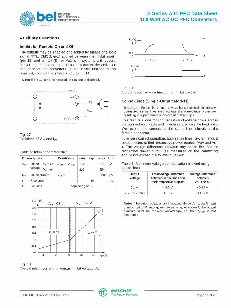
Inhibit for Remote On and OffThe outputs may be enabled or disabled by means of a logicsignal (TTL, CMOS, etc.) applied between the inhibit input i(pin 18) and pin 14 (S– or Vo1–). In systems with severalconverters, this feature can be used to control the activationsequence of the converters. If the inhibit function is notrequired, connect the inhibit pin 18 to pin 14.
Note: If pin 18 is not connected, the output is disabled.
Fig. 17Definition of Vinh and Iinh.
Table 5: Inhibit characteristics
Characteristic Conditions min typ max Unit
Vinh Inhibit Vo = on Vi min – Vi max – 50 0.8 Vvoltage Vo = off 2.4 50
I inh Inhibit current Vinh = 0 – 400 µA
t r Rise time 30 ms
t f Fall time depending on Io
Fig. 19Output response as a function of inhibit control
Fig. 18Typical inhibit current I inh versus inhibit voltage Vinh
0 t
t0
Inhibit
1
0.1
1Vo/Vo nom
tr tf
06001
Sense Lines (Single-Output Models)
Important: Sense lines must always be connected! Incorrectlyconnected sense lines may activate the overvoltage protectionresulting in a permanent short-circuit of the output.
This feature allows for compensation of voltage drops acrossthe connector contacts and if necessary, across the load lines.We recommend connecting the sense lines directly at thefemale connector.
To ensure correct operation, both sense lines (S+, S–) shouldbe connected to their respective power outputs (Vo+ and Vo–). The voltage difference between any sense line and itsrespective power output (as measured on the connector)should not exceed the following values:
Table 6: Maximum voltage compensation allowed usingsense lines
Output Total voltage difference Voltage difference voltage between sense lines and between
their respective outputs Vo– and S–
5.1 V <0.5 V <0.25 V
12 V, 15 V, 24 V <1.0 V <0.25 V
Note: If the output voltages are increased above Vo nom via R-inputcontrol, option P setting, remote sensing, or option T, the outputcurrents must be reduced accordingly, so that Po nom is notexceeded.
S–/Vo1–
i
Vo+Iinh
Vinh
06031b
14
18
Inp
ut
1.6
0.8
0
–0.8Vinh [V]
Iinh [mA]
–40 0–20 20 40
2.0
1.2
0.4
–0.4
Vinh = 0.8 V
Vo = on Vo = off
Vinh = 2.4 V
06032a

S Series with PFC Data Sheet100 Watt AC-DC PFC Converters
BCD20003-G Rev AC, 29-Apr-2015 Page 12 of 28MELCHERThe Power Partners.
R
Vo1+
Vo1–
S–Vext
N~
L~
Rext
R'ext
14
16
16
14
+
S+
Vo1+
Vo1–
S–
N~
L~
R12
06003a
Fig. 20Output voltage control for single-output models LS 4000
Notes:
– The R-Function excludes option P (output voltage adjustmentby potentiometer).
If the output voltages are increased above Vo nom via R-inputcontrol, option P setting, remote sensing or option T, theoutput current(s) should be reduced accordingly so that Po nom
is not exceeded.
– With double-output models the second output follows thevalue of the controlled main output.
– In case of parallel connection the output voltages should beindividually set within a tolerance of 1 – 2%.
Programmable Output Voltage (R-Function)As a standard feature, the converters offer an adjustableoutput voltage, identified by letter R in the type designation.The control input R (pin 16) accepts either a control voltageVext or a resistor Rext to adjust the desired output voltage.When R is not connected, the output voltage is set to Vo nom.
a) Adjustment by means of an external control voltage Vext
between pin 16 (R) and pin 14:
The control voltage range is 0 – 2.75 V and allows anoutput voltage adjustment in the range of approximately0 – 110% Vo nom.
VoVext ≈ –––––– • 2.5 VVo nom
b) Adjustment by means of an external resistor:
Depending upon the value of the required output voltagethe resistor shall be connected
either: Between pin 16 and pin 14 (Vo < Vo nom) to achievean output voltage adjustment range of approx. 0 – 100% Vo
nom.
or: Between pin 16 and pin 12 (Vo > Vo nom) to achieve anoutput voltage adjustment range of approx. 100 – 110% Vo nom.
Warning:
– Vext shall never exceed 2.75 V.
– The value of R'ext shall never be less than the lowest value asindicated in table R'ext (for V0 > V0 nom) to prevent the converterfrom damage!
Table 7a: Rext for Vo < Vo nom; approximate values (Vi nom, Io nom, series E 96 resistors); R'ext = not fitted
Vo nom = 5.1 V Vo nom = 12 V Vo nom = 15 V Vo nom = 24 VVo [V] Rext [kΩ] Vo [V] 1 Rext [kΩ] Vo [V] 1 Rext [kΩ] Vo [V] 1 Rext [kΩ ]
0.5 0.432 2 4 0.806 2 4 0.619 4 8 0.811.0 0.976 3 6 1.33 4 8 1.47 6 12 1.331.5 1.65 4 8 2 6 12 2.67 8 16 22.0 2.61 5 10 2.87 8 16 4.53 10 20 2.872.5 3.83 6 12 4.02 9 18 6.04 12 24 4.023.0 5.76 7 14 5.62 10 20 8.06 14 28 5.623.5 8.66 8 16 8.06 11 22 11 16 32 8.064.0 14.7 9 18 12.1 12 24 16.2 18 36 12.14.5 30.1 10 20 20 13 26 26.1 20 40 205.0 200 11 22 42.2 14 28 56.2 22 44 44.2
Table 7b: R’ext for Vo > Vo nom; approximate values (Vi nom, Io nom, series E 96 resistors); Rext = not fitted
Vo nom = 5.1 V Vo nom = 12 V Vo nom = 15 V Vo nom = 24 V
Vo [V] R'ext [kΩ] Vo [V] 1 R'ext [kΩ] Vo[V]1 R'ext [kΩ] Vo [V] 1 R'ext [kΩ]
5.15 432 12.1 24.2 1820 15.2 30.4 1500 24.25 48.5 33205.2 215 12.2 24.4 931 15.4 30.8 768 24.5 49.0 16905.25 147 12.3 24.6 619 15.6 31.2 523 24.75 49.5 11305.3 110 12.4 24.8 475 15.8 31.6 392 25.0 50.0 8455.35 88.7 12.5 25.0 383 16.0 32.0 316 25.25 50.5 6985.4 75 12.6 25.2 316 16.2 32.4 267 25.5 51.0 5905.45 64.9 12.7 25.4 274 16.4 32.8 232 25.75 51.5 5115.5 57.6 12.8 25.6 243 16.5 33.0 221 26.0 52.0 442
13.0 26.0 196 26.25 52.5 40213.2 26.4 169 26.4 52.8 383
1 First column: Vo or Vo1; second column: double-output models with outputs in series connection

S Series with PFC Data Sheet100 Watt AC-DC PFC Converters
BCD20003-G Rev AC, 29-Apr-2015 Page 13 of 28MELCHERThe Power Partners.
R'extRext
14
16
Vo1–
Vo1+
R
Vo2–
Vo2–
Vo2+
Vo2+
12
10
8
6
4 +
–
Vo1
24 V30 V48 V
Co
06004a
Fig. 21Double-output models: R-input for output voltage control.Wiring for output voltage 24 V, 30 V ,or 48 V with bothoutputs connected in series. A ceramic capacitor (Co) acrossthe load reduces ripple and spikes.
Display Status of LEDs
Vo1 > 0.95 to 0.98Vo1 adj
Vi max Vi ovVi minVi uv
Vi
Vi abs
OKi
Vo1 > 0.95 to 0.98Vo1 adj
Io nom IoL
Io
OKIo L
Vo1 < 0.95 to 0.98Vo1 adj
TC
i
TC max TPTC threshold
Vi inh
i
+50 V+0.8 V +2.4 V-50 V
Vinh threshold
Io L
LED off LED onLED Status undefined
06002_011106
Test JacksTest jacks (pin diameter 2 mm) for measuring the main outputvoltage Vo or Vo1 are located at the front of the converter. Thepositive test jack is protected by a series resistor (seeFunctional Description, block diagrams).
The voltage measured at the test jacks is slightly lower thanthe value at the output terminals.
Fig. 22LED indicators
LEDs "OK ", "i " and "Io L" status versus input voltageConditions: Io ≤ Io nom, TC ≤ TC max, Vinh ≤ 0.8 VVi uv = undervoltage lock-out, Vi ov = overvoltage lockout
LEDs "OK" and "Io L" status versus output currentConditions: Vi min – Vi max, TC ≤ TC max, Vinh ≤ 0.8 V
LED "i " versus case temperatureConditions: Vi min – Vi max , Io ≤ Io nom, Vinh ≤ 0.8 V
LED "i " versus Vinh
Conditions: Vi min – Vi max , Io ≤ Io nom, TC ≤ TC max

S Series with PFC Data Sheet100 Watt AC-DC PFC Converters
BCD20003-G Rev AC, 29-Apr-2015 Page 14 of 28MELCHERThe Power Partners.
2.10
2.15
2.20
2.25
2.30
2.35
2.40
2.45Cell voltage [V]
–20 –10 0 10 20 30 40 50 °C
06139b
VC = 2.27 V, –3 mV/K VC = 2.27 V, –3.5 mV/KVC = 2.23 V, –3 mV/K VC = 2.23 V, –3.5 mV/K
Vo safe
Fig. 23Connection of a temperature sensor
Battery Charging/Temperature SensorThe LS series converters are suitable for battery chargerapplications. For an optimum battery charging and lifeexpectancy of the battery an external temperature sensor canbe connected to the R-input. The sensor is mounted as closeas possible to the battery pole and adjusts the output voltageaccording to the battery temperature.
Fig. 24Trickle charge voltage versus temperature for definedtemperature coefficient.
Powersupply
Load
–+
Input Vo–
R
Temperature sensor
ϑ
03099d
Battery
Vo+
+
Depending upon cell voltage and the temperature coefficientof the battery, different sensor types are available, seeAccessories.

S Series with PFC Data Sheet100 Watt AC-DC PFC Converters
BCD20003-G Rev AC, 29-Apr-2015 Page 15 of 28MELCHERThe Power Partners.
10
40
JM071
dBµV/m TÜV-Divina, Jan.2006Testdistance 10 m, LS4601-7R, Ui=230 VAC, Uo=24 V Io= 4.2 A
50
20
30
EN 55022 B
<25 dbµV/m
Fig. 25Conducted emissions (peak) at the neutral input according toEN 55011/22, measured at Vi nom and Io nom (LS4601-6R). Theline input performs quite similar.
Emissions
0
10
20
30
40
50
60
70
80
0.2 0.5 1 2 5 10 20 MHz
dBµV LS4601-7R, Peak N, Conducted 0.15 - 30 MHz, Divina, Jan. 2006
EN 55022 B
Fig. 26Typ. radiated emissions accord. to EN 55011/22, antenna 10 mdistance, measured at Vi nom and Io nom (LS4601-7R).
Electromagnetic Compatibility (EMC)A metal oxide VDR together with an input fuse and an inputfilter form an effective protection against high input transient
voltages, which typically occur in most installations. The SSeries has been successfully tested to the followingspecifications:
Immunity
Table 11: Electromagnetic immunity (type tests)
Phenomenon Standard Level Coupling Value Waveform Source Test In Perf.mode 1 applied imped. procedure oper. crit. 2
Electrostatic IEC / EN 4 contact discharge 8000 Vp 1/50 ns 330 Ω 10 positive and yes Adischarge 61000-4-2 air discharge 15000 Vp
150 pF 10 negative(to case) discharges
Electromagnetic IEC / EN 3 antenna 10 V/m AM 80% /1 kHz n.a. 80 – 1000 MHz yes Afield 61000-4-3 antenna 20 V/m AM 80% /1 kHz n.a. 800 – 1000 MHz yes A
10 V/m 1400 – 2100 MHz5 V/m 2100 – 2500 MHz
3 antenna 10 V/m 50% duty cycle, n.a. 900 ±5 MHz yes A200 Hz rep. rate pulse modul.
Electrical fast IEC / EN 3 capacitive, o/c ±2000 Vp bursts of 5/50 ns 50 Ω 60 s positive yes Atransients/burst 61000-4-4 ±i/c, +i/–i 2.5/5 kHz over 60 s negative
direct 15 ms; burst transients perperiod: 300 ms coupling mode
Surges IEC / EN 3 ±i/c ±2000 Vp 1.2/50 µs 12 Ω 5 pos. and 5 neg. yes A61000-4-5 +i/– i ±1000 Vp 2 Ω surges per
coupling mode
Conducted IEC / EN 3 i, o, signal wires 10 VAC AM 80% 150 Ω 0.15 – 80 MHz yes Adisturbances 61000-4-6 (140 dBmV) 1 kHz sine wafe
Power frequency IEC / EN 3 -- 100 A/m 60 s in all 3 axis yes Amagnetic field 61000-4-8
Pulse IEC / EN - -- ±300 A/m 5 pulses per axis yes Bmagnetic field 61000-4-9 repetit. rate 10 s
1 i = input, o = output, c = case2 A = Normal operation, no deviation from specifications, B = Temporary loss of function or deviation from specs possible3 For converters with version V102 or higher. Older LKP models meet only B.4 Only LKP models have been tested.
S Series with PFC Data Sheet100 Watt AC-DC PFC Converters
BCD20003-G Rev AC, 29-Apr-2015 Page 16 of 28MELCHERThe Power Partners.
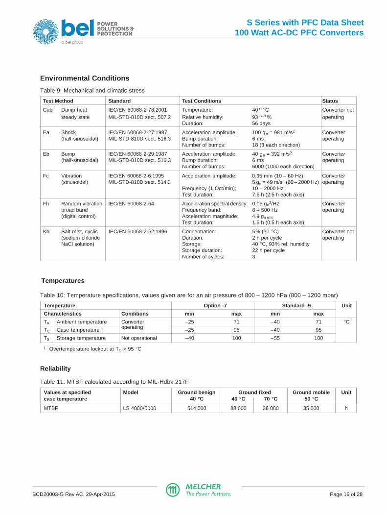
Temperatures
Table 11: MTBF calculated according to MIL-Hdbk 217F
Values at specified Model Ground benign Ground fixed Ground mobile Unitcase temperature 40 °C 40 °C 70 °C 50 °C
MTBF LS 4000/5000 514 000 88 000 38 000 35 000 h
Reliability
Table 10: Temperature specifications, values given are for an air pressure of 800 – 1200 hPa (800 – 1200 mbar)
Temperature Option -7 Standard -9 Unit
Characteristics Conditions min max min max
TA Ambient temperature Converter –25 71 –40 71 °C
TC Case temperature 1 operating –25 95 –40 95
TS Storage temperature Not operational –40 100 –55 100
1 Overtemperature lockout at TC > 95 °C
Environmental Conditions
Table 9: Mechanical and climatic stress
Test Method Standard Test Conditions Status
Cab Damp heat IEC/EN 60068-2-78:2001 Temperature: 40 ±2 °C Converter notsteady state MIL-STD-810D sect. 507.2 Relative humidity: 93 +2/-3 % operating
Duration: 56 days
Ea Shock IEC/EN 60068-2-27:1987 Acceleration amplitude: 100 gn = 981 m/s2 Converter(half-sinusoidal) MIL-STD-810D sect. 516.3 Bump duration: 6 ms operating
Number of bumps: 18 (3 each direction)
Eb Bump IEC/EN 60068-2-29:1987 Acceleration amplitude: 40 gn = 392 m/s2 Converter(half-sinusoidal) MIL-STD-810D sect. 516.3 Bump duration: 6 ms operating
Number of bumps: 6000 (1000 each direction)
Fc Vibration IEC/EN 60068-2-6:1995 Acceleration amplitude: 0.35 mm (10 – 60 Hz) Converter(sinusoidal) MIL-STD-810D sect. 514.3 5 gn = 49 m/s2 (60 – 2000 Hz) operating
Frequency (1 Oct/min): 10 – 2000 HzTest duration: 7.5 h (2.5 h each axis)
Fh Random vibration IEC/EN 60068-2-64 Acceleration spectral density: 0.05 gn2/Hz Converter
broad band Frequency band: 8 – 500 Hz operating(digital control) Acceleration magnitude: 4.9 gn rms
Test duration: 1.5 h (0.5 h each axis)
Kb Salt mist, cyclic IEC/EN 60068-2-52:1996 Concentration: 5% (30 °C) Converter not(sodium chloride Duration: 2 h per cycle operatingNaCl solution) Storage: 40 °C, 93% rel. humidity
Storage duration: 22 h per cycleNumber of cycles: 3

S Series with PFC Data Sheet100 Watt AC-DC PFC Converters
BCD20003-G Rev AC, 29-Apr-2015 Page 17 of 28MELCHERThe Power Partners.
111
(3U
)
168.5
60
4.5
19.7
9.5
29.9
51.5
30.3
20.3
12.1
10.3
7.0
3.277 TE 5 TE
Test jacks
Option P (Vo)
Option D (Vti)
LED OK (green)
LED i (red)
LED IoL (red)
Option D (Vto)
25.9
Front plate Main face Back plate
(171.0 to 171.9)
50
11.8
= Ø 3.5= Ø 4.1
(+/–)
152
100
M4
55
81528
0900
4f
Measuring point ofcase temperature TC
d
= Ø 4.1= Ø 3.5
Screw holes of thefrontplate
∅ 5 x 90°
∅ 2.8 0.2
Mechanical DataDimensions in mm. The converters are designed to be inserted intoa 19" rack, 160 mm long, according to IEC 60297-3.
EuropeanProjection
Notes:
– d ≥ 15 mm, recommended minimum distance tonext part in order to ensure proper air circulationat full output power.
– free air location: the converter should be moun-ted with fins in a vertical position to achievemaximum airflow through the heat sink.
Fig. 27Aluminum case S02 with heat sink;black finish (EP powder coated);weight approx. 1.25 kg

S Series with PFC Data Sheet100 Watt AC-DC PFC Converters
BCD20003-G Rev AC, 29-Apr-2015 Page 18 of 28MELCHERThe Power Partners.
6.5
11.2
13
140
17.3 133.4 ±0.230
168
5 47.2
38.5
127
6.5
11.8
11027
EuropeanProjection
111
(3U
)
17.3 133.4
168
101
547.2
1585
M 4
5
Measuring point ofcase temperature TC
50
(171.0 ... 171.9)
3.27
7 TE 4 TE
09003b
38.5
11.8
Fig. 28Option B1: Aluminium case S02 with small cooling plate; black finish (EP powder coated).Suitable for mounting with access from the backside.Total weight approx. 1.2 kg.
Fig. 29Option B: Aluminium case S02 with large cooling plate; black finish (EP powder coated).Suitable for front mounting.Total weight approx. 1.3 kg
Note: Long case with option B2, elongated by 60 mm for 220 mmrack depth, is available on request. (No LEDs, no test jacks.)

S Series with PFC Data Sheet100 Watt AC-DC PFC Converters
BCD20003-G Rev AC, 29-Apr-2015 Page 19 of 28MELCHERThe Power Partners.
Fig. 30View of converter's male connector, type H15
Safety and Installation Instructions
Connector Pin AllocationThe connector pin allocation table defines the electricalpotentials and the physical pin positions on the H15connector. The protective earth is connected trough a leadingpin (no. 24), ensuring that it makes contact with the femaleconnector first.
Installation Instructions
Important: These products have a power factor correction (PFC)and are intended to replace the LS1000 and LS2000 seriesconverters, in order to comply with IEC/EN 61000-3-2.
Switch off the system and check for hazardous voltagesbefore altering any connection!
These converters are components, intended exclusively forinclusion within other equipment by an industrial assemblyoperation or by professional installers. The installation must
S10002b
32 28 24 20 16 12 8 4
30 26 22 18 14 10 6
Fixtures for retention clips
strictly follow the national safety regulations in compliancewith the enclosure, mounting, creepage, clearance, casualty,markings, and segregation requirements of the end-useapplication.
Connection to the system shall be made via the femaleconnector H15 (see Accessories). Other installation methodsmay not meet the safety requirements.
Pin no. 24 ( ) is reliably connected with the case. For safetyreasons, it is essential to connect this pin reliably to protectiveearth. See Safety of Operator-Accessible Output Circuits.
The phase input 30/32 (L~) is connected via a built-in fuse(see Input Fuse), which is designed to protect in the case of aconverter failure. An additional external fuse, suitable for theapplication, might be necessary in the wiring to the other lineinput 26/28 (N~) if:
• Local requirements demand an individual fuse in eachsource line
• Neutral and earth impedance is high or undefined
• Phase and neutral of the mains are not defined or cannotbe assigned to the corresponding terminals (L~ to phaseand N~ to neutral).
Notes:
– If the inhibit function is not used, pin no. 18 (i) should beconnected to pin no. 14 (S– /Vo1–) to enable the output(s).
– Do not open the converters, or warranty will be invalidated.
– Due to high current values, the converters provide twointernally parallel contacts for certain paths (pins 4/6, 8/10, 26/28 and 30/32). It is recommended to connect load and supply toboth female connector pins of each path in order to keep thevoltage drop low and to not overstress the connector contactswith high currents.
– If the second output of double-output models is not used, connectit parallel with the main output.
Make sure that there is sufficient airflow available forconvection cooling. This should be verified by measuring thecase temperature, when the converter is installed andoperated in the end-use application. See Thermal Con-siderations.
Ensure that a converter failure (e.g., by an internal short-circuit) does not result in a hazardous condition. See alsoSafety of Operator-Accessible Output Circuit.
Standards and ApprovalsThe converters are safety-approved to EN/IEC 60950-1, andUL/CSA 60950-1 2 nd Ed. (version 106 or greater).
The converters correspond to Class I equipment and havebeen evaluated for:
• Building-in
• Basic insulation between input and case based on 250VAC, and double or reinforced insulation between input andoutput(s).
• Functional insulation between outputs.
• Overvoltage category II
Table 12: Pin allocation
Pin Connector type H15
no. LS4000 LS5000
4Vo1+ Positive output Vo2+ Pos. output 2
6
8Vo1– Negative output Vo2– Neg. output 2
10
12 S+ Sense+ Vo1+ Output 1
14 S– Sense– Vo1– Output 1
16 R 1 Control of Vo1 R 1 Control of Vo1
18 i Inhibit i Inhibit
20D 3 Save data
D 3 Save dataV 3 ACFAIL
22 T 4 Current share T 4 Current share
24 2 Protective earth Protective earth
26N~ Neutral line N~ Neutral line
28
30L~ Phase line L~ Phase line
32
1 Not connected, if option P is fitted2 Leading pin (pre-connecting)3 Option D excludes option V and vice versa. Pin is not connec-
ted, if neither option D or V is fitted.4 Not connected, unless option T is fitted.

S Series with PFC Data Sheet100 Watt AC-DC PFC Converters
BCD20003-G Rev AC, 29-Apr-2015 Page 20 of 28MELCHERThe Power Partners.
• Pollution degree 2 environment
• Max. altitude: 2000 m.
• The converters fulfill the requirements of a fireenclosure.
All boards of the converters are coated with aprotective lacquer.
The converters are subject to manufacturing surveillancein accordance with the above mentioned UL standards andISO 9001:2008. CB-scheme is available.
Protection Degree and Cleaning LiquidsCondition: Female connector fitted to the converter.
• IP 30: All models except those with option P, and exceptthose with option D or V including a potentiometer.
• IP 20: All models fitted with option P, or with option D or Vwith potentiometer.
In order to avoid possible damage, any penetration ofcleaning fluids is to be prevented.
Isolation and Leakage CurrentsThe electric strength test is performed in the factory as routinetest in accordance with EN 50514 and IEC/EN 60950. Thecompany will not honor warranty claims resulting fromincorrectly performed electric strength field tests.
Leakage currents flow due to internal leakage capacitances andY-capacitors. The current values are proportional to the supplyvoltage and are specified in the table below.
Table 13: Isolation
Characteristic Input to case Output(s) to Output 1 to Unitand output(s) case output 2
Electric Factory test >1 s 2.8 1 1.4 0.15 kVDCstrength AC test voltage equivalent
2.0 1.0 0.1 kVACtest to factory test
Insulation resistance at 500 VDC >300 >300 >100 2 MΩCreapage distances ≥ 3.2 3 -- -- mm
1 According to IEC/EN 60950, subassemblies connecting input to output are pre-tested with 5.6 kVDC or 4 kVAC.2 Tested at 150 VDC3 Input to outputs: 6.4 mm
Table 14: Leakage currents
Characteristic Class I Unit
Maximum earth Permissible according to IEC/EN 60950 3.5 mAleakage current Typ. value at 254 V, 50 Hz (LS models) 0.8
Fig. 31Schematic safety concept.
Railway Applications and Fire ProtectionThe converters have been designed by observing the railwaystandards EN 50155 and EN 50121-4. All boards are coatedwith a protective lacquer.
The converters with version V108 (or later) comply with NF-F16(I2/F1). They also accord to EN 45545-1, EN 45545-2 (2013),if installed in a technical compartment or cabinet.
Safety of Operator-Accessible Output CircuitIf the output circuit of an converter is operator-accessible, itshall be an SELV circuit according to IEC/EN 60950 .
The table below shows a possible installation configuration,compliance with which causes the output circuit of an S SeriesAC-DC converter to be an SELV circuit according to IEC/EN60950 up to a configured output voltage of 36 V (sum of nominaloutput voltages connected in series) .
Table 15: Safety concept leading to an SELV output circuit
Conditions AC-DC converter Installation Result
Nominal voltage Grade of insulation Measures to achieve the resulting Safety status of the AC-DCbetween input and output safety status of the output circuit converter output circuitprovided by the AC-DC converter
Mains Double or reinforced Earthed case1 and installation SELV circuit≤ 250 VAC according to the applicable standards
1 The earth connection has to be provided by the installer according to the relevant safety standards, e.g. IEC/EN 60950.
AC-DCcon-
verter
Mains SELV
Earthconnection
+
–
~
~
10021a
Fuse
Fuse

S Series with PFC Data Sheet100 Watt AC-DC PFC Converters
BCD20003-G Rev AC, 29-Apr-2015 Page 21 of 28MELCHERThe Power Partners.
--7 Restricted Temperature RangeOption -7 and -7E stand for a restricted operational ambienttemperature range of –25 to 71 °C rather than – 40 to 71 °C.
E Inrush Current LimitationThe converters exhibit an electronic circuit replacing thestandard built-in NTC, in order to achieve an enhanced inrushcurrent limiting function (standard feature).
Note: Subsequent switch-on cycles at start-up are limited to max.10 cycles during the first 20 seconds (cold converter) and then tomax. 1 cycle every 8 s.
Fig. 32Option E block diagram
Description of Options
Table 16: Survey of options
Option Function of option Characteristic
-7, -7E Extended operational ambient temperature range TA = – 25 to 71 °C
E Electronic inrush current limitation circuitry Active inrush current limitation, standard feature for TA = – 40 °C
P 2 Potentiometer for fine adjustment of output voltage Adjustment range +10/– 60% of Vo nom, excludes R input
D1 Input and/or output undervoltage monitoring circuitry Safe data signal output (D0 – DD)
V1 Input and/or output undervoltage monitoring circuitry ACFAIL signal according to VME specifications (V0, V2, V3)
T Current sharing Interconnect T-pins if paralleling outputs (max 5 converters)
B, B1, B2 Cooling plate (160 or 220 mm long) Replaces standard heat sink, allowing direct chassis-mounting
G RoHS-compliant for all six substances G is always the last character in the type designation
1 Option D excludes option V and vice versa; option V only for 5.1 V outputs.2 Option P is not available for battery charger models.
Inpu
t Filt
er
Control
Con
vert
er
FET
CbRI
Rectifier PF
C -
cor
rect
.
11001b
+
Rs
Table 17: Inrush current characteristics with option E
Characteristics LS UnitVi = 230 VAC typ max
Iinr p Peak inrush current – 25.3 A
t inr Inrush current duration 35 50 ms
P PotentiometerA potentiometer provides an output voltage adjustment rangeof +10/–60% of Vo nom. It is accessible through a hole in thefront cover. Option P is not available for battery chargermodels and is not recommended for converters connected inparallel.
Option P excludes the R-function. With double-outputmodels,both outputs are influenced by the potentiometersetting (doubling the voltage, if the outputs are in series).
If the output voltages are increased above Vo nom via R inputcontrol, option P setting, remote sensing or option T, theoutput current(s) should be reduced accordingly, so thatPo nom is not exceeded.
Fig. 33Inrush current with option EVi = 230 VAC, f i = 50 Hz, Po = Po nom
15
Ii [A]
10
5
0
–5
–10
0 20 40 60 80 ms
t tinr
Capacitor Cifully charged
Normal operation(FET fully conducting)
20
10 50 7030
11002b
S Series with PFC Data Sheet100 Watt AC-DC PFC Converters
BCD20003-G Rev AC, 29-Apr-2015 Page 22 of 28MELCHERThe Power Partners.
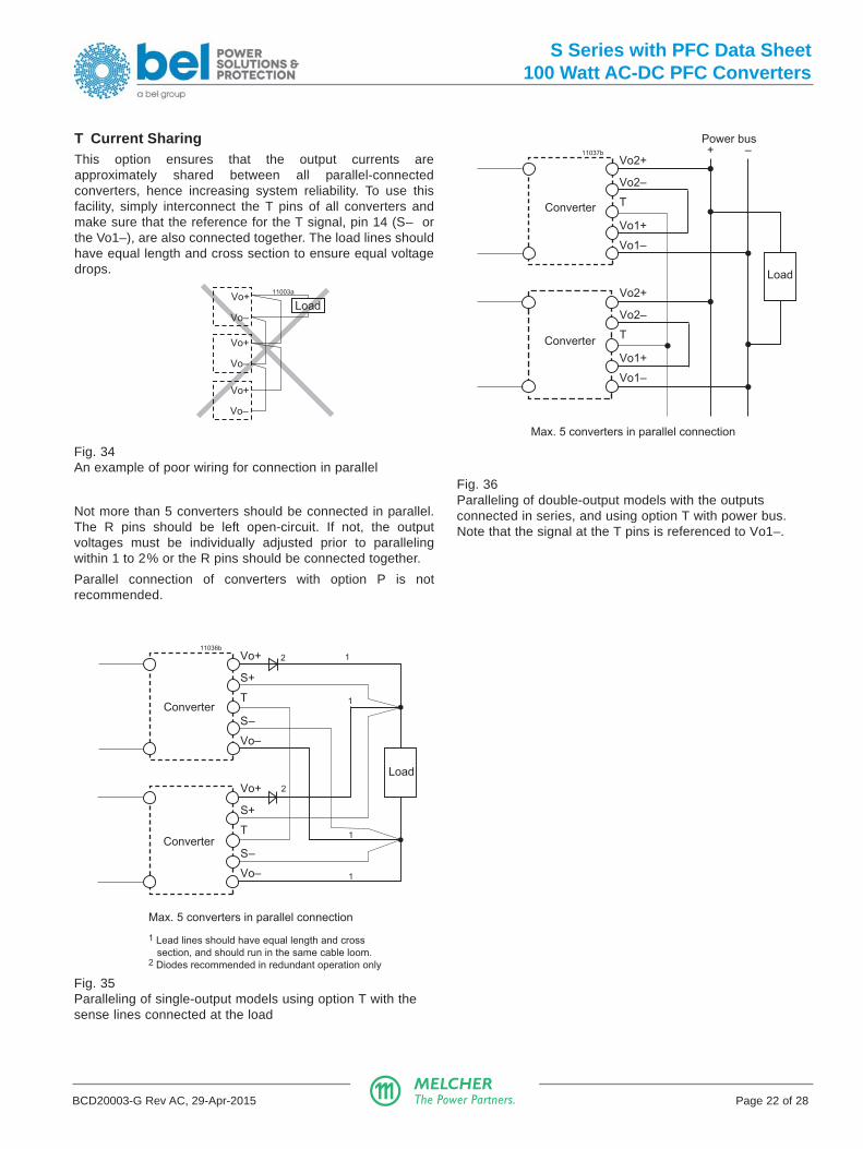
Fig. 35Paralleling of single-output models using option T with thesense lines connected at the load
Fig. 36Paralleling of double-output models with the outputsconnected in series, and using option T with power bus.Note that the signal at the T pins is referenced to Vo1–.
T Current SharingThis option ensures that the output currents areapproximately shared between all parallel-connectedconverters, hence increasing system reliability. To use thisfacility, simply interconnect the T pins of all converters andmake sure that the reference for the T signal, pin 14 (S– orthe Vo1–), are also connected together. The load lines shouldhave equal length and cross section to ensure equal voltagedrops.
Fig. 34An example of poor wiring for connection in parallel
Not more than 5 converters should be connected in parallel.The R pins should be left open-circuit. If not, the outputvoltages must be individually adjusted prior to parallelingwithin 1 to 2% or the R pins should be connected together.
Parallel connection of converters with option P is notrecommended.
Vo+
Vo–
Vo+
Vo–
Load
Vo+
Vo–
11003a
Load
1
1
1
2
2
S+
Vo+
Vo–
S–
T
S+
Vo+
Vo–
S–
T
1
Max. 5 converters in parallel connection
1 Lead lines should have equal length and cross section, and should run in the same cable loom.2 Diodes recommended in redundant operation only
11036b
Converter
Converter
Load
Max. 5 converters in parallel connection
+ –Power bus
Converter
Vo2–
Vo2+
Vo1–
Vo1+
T
Converter
Vo2–
Vo2+
Vo1–
Vo1+
T
11037b

S Series with PFC Data Sheet100 Watt AC-DC PFC Converters
BCD20003-G Rev AC, 29-Apr-2015 Page 23 of 28MELCHERThe Power Partners.
Vo+/Vo1+
S–/Vo1–
D
VD
ID
Rp
Inpu
t
11007a
NPN opencollector
20
14
D Undervoltage MonitorThe input and/or output undervoltage monitoring circuitoperates independently of the built-in input undervoltagelockout circuit. A logic "low" (self conducting JFET) or "high"signal (NPN output) is generated at the D output (pin 20),when one of the monitored voltages drops below thepreselected threshold level Vt. This signal is referenced to S–/Vo1–. The D output recovers, when the monitored voltagesexceed Vt + Vh. The threshold level Vbi is adjusted in thefactory. The threshold level Vto is either adjusted by apotentiometer accessible through a hole in the front cover, oradjusted in the factory to a fixed value specified by thecustomer.
Option D exists in various versions D0 – DD, as shown in thetable below.
JFET output (D0 – D4):
Pin D is internally connected via the drain-source path of aJFET (self-conducting type) to the negative potential of output1. VD ≤ 0.4 V (logic low) corresponds to a monitored voltagelevel (Vi and/or Vo1) <Vt. The current ID through the JFETshould not exceed 2.5 mA. The JFET is protected by a 0.5 WZener diode of 8.2 V against external overvoltages.
Fig. 37Option D0 – D4: JFET output, I D ≤ 2.5 mA
Fig. 38Option D5 – DD: NPN output, Vo1 ≤ 40 V, ID ≤ 20 mA
Vo+/Vo1+
S–/Vo1–
D
VD
ID
Rp
Inpu
t
11006a
Self-conducting junction FET
20
14
NPN output (D5 – DD):
Pin D is internally connected via the collector-emitter path of aNPN transistor to the negative potential of output 1. VD < 0.4 V(logic low) corresponds to a monitored voltage level (Vi and/orVo1) > Vt + Vh. The current ID through the open collector shouldnot exceed 20 mA. The NPN output is not protected againstexternal overvoltages. VD should not exceed 40 V.
Table 19: JFET output (D0 – D4)
Vb, Vo1 status D output, VD
Vb or Vo1 < Vt low, L, VD ≤ 0.4 V at ID = 2.5 mA
Vb and Vo1 > Vt + Vh high, H, ID ≤ 25 µA at VD = 5.25 V
Table 18: Undervoltage monitoring functions
Output type Monitoring Minimum adjustment range Typical hysteresis Vho [% of Vt]JFET NPN Vb 4 Vo/Vo1 of threshold level Vt for Vt min – Vt max
Vtb 4 Vto Vho
D1 D5 no yes - 3.5 – VBR 1 2.5 – 0.6 V
D2 D6 yes no 355 VDC - -
D3 D7 yes yes 355 VDC (0.95 – 0.985 Vo1) 2 "0"
D4 D8 no yes - (0.95 – 0.985 Vo1) 2 "0"
D0 D9 no yes - 3.5 – VBR 3 2.5 – 0.6 V
yes yes 355 VDC 3.5 – VBR 3 2.5 – 0.6 V
DD yes yes 355 VDC 3.5 – VBR 1 2.5 – 0.6 V
1 Threshold level adjustable by potentiometer. See Output Data for VBR.2 Fixed value. Tracking if Vo1 is adjusted via R-input, option P, or sense lines.3 The threshold level permanently adjusted according to customer specification ±2% at 25 °C. Any value within the specified range is
basically possible, but causes a special type designation in addition to the standard option designations (D0/D9).4 Vb is the voltage generated by the boost regulator. When Vb drops below 355 V, the D signal triggers, and the output(s) will remain
powered during nearly the full hold-up time t h.
Table 20: JFET output (D5 – DD)
Vb, Vo1 status D output, VD
Vb or Vo1 < Vt high, H, ID ≤ 25 µA at VD = 40 V
Vb and Vo1 > Vt + Vh low, L, VD ≤ 0.4 V at ID = 20 mA

S Series with PFC Data Sheet100 Watt AC-DC PFC Converters
BCD20003-G Rev AC, 29-Apr-2015 Page 24 of 28MELCHERThe Power Partners.
0
10.95
0
Vb [VDC]
0
t
t
t
tlow min
4 tlow min4 thigh min
th1
358
355
Input voltage failure Switch-on cycle Input voltage sag Switch-on cycle and subsequentinput voltage failure
VD high
VD low
VD
0
JFET
NPN
t
Vo1Vo1 nom
VD high
VD low
VD
tlow min4th
1
0
0
VD high
VD low
VD
0
JFET
NPN
Vo1
VD high
VD low
VD
tlow min4
Vto
Output voltage failure
0
ID high
ID low
ID
t
0
ID high
ID low
ID
t
t
t
t
2
3 3 3 3
Vo1 nomVto +Vho
Input voltage monitoring
Output voltage monitoring
11044b
1 Hold-up time see: Electrical Input Data.2 With output voltage monitoring, hold-up time t h = 0.3 The signal remains high, if the D output is connected
to an external source.4 t low min = 100 – 170 ms, typically 130 ms.
Fig. 39Relationship between Vb, Vo1, VD, Vo1/Vo1 nom versustime
Table 21: D-output logic signals
Version of D Vb <<<<< Vt resp. Vo <<<<< Vt Vb >>>>> Vt + Vh resp. Vo >>>>> Vt Configuration
D1, D2, D3, D4, D0 low high JFET
D5, D6, D7, D8, D9, DD high low NPN

S Series with PFC Data Sheet100 Watt AC-DC PFC Converters
BCD20003-G Rev AC, 29-Apr-2015 Page 25 of 28MELCHERThe Power Partners.
3
5.1 V4.875 V
0
Vb [VDC]
0
t
t
358355
Input voltage failure Switch-on cycle Input voltage sag Switch-on cycle and subsequentinput voltage failure
VV high
VV low
VV
0
V2
t
Vo
0
VV high
VV low
VV
0
V2
Vi
Vti
4
Output voltage failure
0
VV high
VV low
VV
3
Vti + Vhi
tlow min 2 tlow min
2tlow min 2
3 3
44
VV high
VV low
VV
0
V3
t
3
tlow min 2tlow min
2
3 3
th 1
2.0 V
th 1
4
34
tlow min 2
V3
5.1 V4.875 V
0
Vo
2.0 V
Input voltage monitoring
Output voltage monitoring
11045a
t
t
t
t
Fig. 40Vcb, Vo, VV, IV, Vo /Vo nom versus time.
1 VME request: minimum 4 ms2 t low min = 40 – 200 ms, typ 80 ms3 VV level not defined at Vo < 2.0 V4 The V signal drops simultaneously with the output
voltage, if the pull-up resistor R P is connected to Vo+;the V signal remains high if R P is connected to anexternal source.
V ACFAIL Signal (VME)
Available only for models with Vo = 5.1 V.
This option defines an undervoltage monitoring circuit forthe input and main output voltage. It generates the ACFAILsignal (V signal) according to the VME standard.
The low state level of the ACFAIL signal is specified at a sinkcurrent of IV ≤ 48 mA to VV ≤ 0.6 V (open-collector output of anNPN transistor). The pull-up resistor feeding the open-collector output should be placed on the VME backplane.

S Series with PFC Data Sheet100 Watt AC-DC PFC Converters
BCD20003-G Rev AC, 29-Apr-2015 Page 26 of 28MELCHERThe Power Partners.
Fig. 41Output configuration of options V2 and V3
B, B1, B2 Cooling PlateWhere a cooling surface is available, we recommend the useof a cooling plate instead of the standard heat sink. Themounting system should ensure sufficient cooling capacity toguarantee that the maximum case temperature TC max is notexceeded. The cooling capacity is calculated by:
(100% – η)PLoss = –––––––––– • Vo • Io
η
Efficiency η see Model Selection
For the dimensions of the cooling plates, see Mechnical Data.Option B2 is for customer-specific models with elongatedcase (for 220 mm DIN-rack depth).
G RoHSModels with G as last character of the type designation areRoHS-compliant for all six substances.
Vo+
S–
V
VV
IVRp
Inpu
t
11009a
NPN opencollector
20
14
After the ACFAIL signal has gone low, the VME standardrequires a hold-up time th of at least 4 ms before the 5.1 Voutput drops at full load to 4.875 V. This hold-up time t h isprovided by the capacitance supporting the boost voltage Vb.See Hold-up Time.
Table 22: Undervoltage monitor functions
V output Monitoring Minimum adjustment (VME compatible) Vb Vo1 range of threshold level
Vt b Vt o
V2 yes no 355 VDC 1 –
V3 yes yes 355 VDC 1 0.95 – 0.985 Vo1 2
1 Option V monitors Vb generated by the boost regulator. Thetrigger level is adjusted in the factory to 355 VDC.
2 Fixed value between 95% and 98.5% of Vo1
Option V operates independently of the built-in inputundervoltage lockout circuit. A logic "low" signal is generatedat pin 20, as soon as one of the monitored voltages dropsbelow the preselected threshold level Vt. The return for thissignal is S– or Vo1–. The V output recovers, when themonitored voltage(s) exceed(s) Vt + Vh. The threshold levelVto is adjusted in the factory to a customer-specified value.
V-output (V2, V3):
Connector pin V is internally connected with the opencollector of an NPN transistor. The emitter is connected withS– orVo1–. VV ≤ 0.6 V (logic low) corresponds to a monitoredvoltage level (Vi and/or Vo) <Vt. The current IV through theopen collector should not exceed 50 mA. The NPN output isnot protected against external overvoltages. VV should notexceed 60 V.
Table 23: Status of V output
Vb, Vo status V output, VV
Vb or Vo < Vt low, L, VV ≤ 0.6 V at IV = 50 mA
Vb and Vo1 > Vt + Vh high, H, IV ≤ 25 µA at VV = 5.1 V

S Series with PFC Data Sheet100 Watt AC-DC PFC Converters
BCD20003-G Rev AC, 29-Apr-2015 Page 27 of 28MELCHERThe Power Partners.
AccessoriesA variety of electrical and mechanical accessories areavailable including:
– Front panels for 19" DIN-rack: Schroff or Intermas,12 TE /3U; see fig. 42.
– Mating H15 connectors with screw, solder, faston, orpress-fit terminals, code key system and coding wedgesHZZ00202-G; see fig. 43.
– Pair of connector retention clips HZZ01209-G; see fig. 44
– Connector retention brackets HZZ01216-G; see fig. 45.
– Cage clamp adapter HZZ00144-G; see fig. 46
– Different cable hoods for H15 connectors (fig. 47):
- HZZ00141-G, screw version- HZZ00142-G, use with retention brackets HZZ01218-G- HZZ00143-G, metallic version providing fire protection
Fig. 44Connector retention clips to fasten the H15 connector tothe rear plate; see fig. 24. HZZ01209-G consists of 2 clips.
Fig. 46Cage clamp adapter HZZ00144-G
Fig. 42Different front panels
Fig. 43Different mating connectors
Fig. 45Connector retention brackets HZZ01216-G (CRB-HKMS)
20 to 30 Ncm
Fig. 47Different cable hoods

S Series with PFC Data Sheet100 Watt AC-DC PFC Converters
BCD20003-G Rev AC, 29-Apr-2015 Page 28 of 28MELCHERThe Power Partners.
NUCLEAR AND MEDICAL APPLICATIONS - These products are not designed or intended for use as critical components in life supportsystems, equipment used in hazardous environments, or nuclear control systems.
TECHNICAL REVISIONS - The appearance of products, including safety agency certifications pictured on labels, may change depending onthe date manufactured. Specifications are subject to change without notice.
Copyright © 2015, Bel Power Solutions Inc. All rights reserved. www.belpowersolutions.com/power
Fig. 48Chassis- or wall-mounting plateHZZ01213-G (Mounting plate K02)
56 (2.2")L
L = 2 m (standard length) other cable lengths on request
adhesive tape
26 (1.02")
9.8
(0.4
")09125a
Fig. 49DIN-rail mounting assembly HZZ00615-G (DMB-K/S)
EuropeanProjection
Table 24: Battery temperature sensors
Battery Sensor Cell Cell temp. Cablevoltage type voltage coefficient lengthnom. [V] [V] [mV/K] [m]
12 S-KSMH12-2.27-30-2 2.27 –3.0 2
12 S-KSMH12-2.27-35-2 2.27 –3.5 2
24 S-KSMH24-2.27-30-2 2.27 –3.0 2
24 S-KSMH24-2.27-35-2 2.27 –3.5 2
24 S-KSMH24-2.31-35-0 2.31 –3.5 4.5
24 S-KSMH24-2.31-35-2 2.31 –3.5 2
24 S-KSMH24-2.35-35-2 2.35 –3.5 2
48 S-KSMH48-2.27-30-2 2.27 –3.0 2
48 S-KSMH48-2-27-35-2 2.27 –3.5 2
Fig. 50Battery temperature sensor
Note: Other temperature coefficients and cable lengths areavailable on request.
– Chassis or wall-mounting plate K02 (HZZ01213-G) formodels with option B1. Mating connector (HZZ00107-G)with screw terminals; see fig. 48
– DIN-rail mounting assembly HZZ0615-G (DMB-K/S); seefig. 49
– Additional external input and output filters
– Different battery sensors S-KSMH... for using theconverter as a battery charger. Different cellcharacteristics can be selected; see fig. 32, table 12, andBattery Charging /Temperature Sensors.
For additional accessory product information, see theaccessory data sheets listed with each product series orindividual model at our web site:
www.belpowersolutions.com/power