Embed Size (px)
Citation preview
Mitsubishi Programmable Controller
Analog-Digital Converter Module type AJ65VBTCU-68ADV/ADI
User,s Manual
Specifications subject to change without notice.
MODEL
MODELCODE
AJ65V-68AD-U-SY-E
13JR41
SH(NA)-080181-A(0107)MEE
Analog-Digital Converter Module type AJ65VBTCU-68ADV/ADI
User,s Manual
U
An
alo
g-D
igita
l Co
nve
rter M
od
ule
type
AJ6
5V
BT
CU
-68A
DV
/AD
I Use
r ,s Manual
When exported from Japan, this manual does not require application to theMinistry of Economy, Trade and Industry for service transaction permission.
HEAD OFFICE : 1-8-12, OFFICE TOWER Z 14F HARUMI CHUO-KU 104-6212,JAPANNAGOYA WORKS : 1-14 , YADA-MINAMI 5 , HIGASHI-KU, NAGOYA , JAPAN
A - 1 A - 1
SAFETY PRECAUTIONS (Always read these precautions before using this equipment.)
Before using this product, please read this manual and the relevant manuals introduced in this manualcarefully and pay full attention to safety to handle the product correctly.The precautions given in this manual are concerned with this product. Refer to the user’s manual of theCPU module to use for a description of the PLC system safety precautions.In this manual, the safety instructions are ranked as "DANGER" and "CAUTION".
! DANGER
CAUTION!
Indicates that incorrect handling may cause hazardous conditions,resulting in death or severe injury.
Indicates that incorrect handling may cause hazardous conditions, resulting in medium or slight personal injury or physical damage.
Note that the ! CAUTION level may lead to a serious consequence according to the circumstances.Always follow the precautions of both levels because they are important to personal safety.
Please save this manual to make it accessible when required and always forward it to the end user.
[Design Precautions]! DANGER
When there are communication problems with the data link, the data for the master module willbe held.Configure an interlocking circuit in a sequence program so that the safety of the overall systemis always maintained.
! CAUTION Do not bunch the control wires or communication cables with the main circuit or power wires, orinstall them close to each other.They should be installed 100mm (3.9inch) or more from each other.Not doing so could result in noise that would cause erroneous operation.
A - 2 A - 2
[Installation Precautions]! CAUTION
Use the PLC in the environment that meets the general specifications contained in this Manual.Using the PLC outside the range of the general specifications may result in electric shock, fire ormalfunction, or may damage or degrade the module.
Securely fix the module to a DIN rail or securely fix it with the CC-Link connector type metalinstallation fitting.Not doing so can cause a drop or malfunction.
Do not touch the conducted area or electric parts of the module.Doing so may cause module malfunctioning or breakdowns.
[Wiring Precautions]! CAUTION
Always switch power off externally in all phases before starting installation, wiring and otherworks.Not doing so can cause the product to be damaged or malfunction.
Always ground the FG pin and FG1 pin to the protective ground conductor.Not doing so can cause a malfunction.
Wire the module correctly after confirming the rated voltage and pin layout of the product.Not doing so can cause a fire or failure.
Ensure that no foreign matter such as chips and wire-offcuts enter the module.Foreign matter can cause a fire, failure or malfunction.
Do not insert the one-touch connector plug for I/O of the one-touch connector type/connectortype compact remote I/O unit into the one-touch connector for analog I/O accidentally.Doing so can cause the module to be damaged.
Always fit a non-wired, one-touch connector plug to the open one-touch connector for powersupply/FG.Not doing so can cause a failure or malfunction.
When connecting the communication and power supply cables to the module, always run themin conduits or clamp them.Not doing so can damage the module and cables due to loose, moved or accidentally pulledcables or can cause a malfunction due to a cable connection fault.
When disconnecting the communication and power supply cables from the module, do not holdand pull the cable part.Disconnect the cables after loosening the screws in the portions connected to the module.Pulling the cables connected to the module can damage the module and cables or can cause amalfunction due to a cable connection fault.
A - 3 A - 3
[Starting and Maintenance Precautions]! CAUTION
Do not touch the pin while the power is on. Doing so may cause malfunction. Always start cleaning after switching power off externally in all phases.Not doing so can cause the module to fail or malfunction.
Never disassemble or modify the module.This may cause breakdowns, malfunctioning, injury and/or fire.
Do not drop the module or give it hard impact since its case is made of resin. Doing so candamage the module.
Mount or dismount the module to or from an enclosure after switching power off externally in allphases.Not doing so can cause the module to fail or malfunction.
[Disposal Precautions]! CAUTION
When disposing of this product, treat it as industrial waste.
A - 4 A - 4
REVISIONS* The manual number is given on the bottom left of the back cover.
Print Date * Manual Number RevisionJul., 2001 SH (NA)-080181-A First PrintingOct., 2001 SH (NA)-080181-B Correction
Section 2.3, Section 3.2, Appendix 2
Japanese Manual Version SH-080183-A
This manual confers no industrial property rights or any rights of any other kind, nor does it confer any patentlicenses. Mitsubishi Electric Corporation cannot be held responsible for any problems involving industrial propertyrights which may occur as a result of using the contents noted in this manual.
2001 MITSUBISHI ELECTRIC CORPORATION
A - 5 A - 5
INTRODUCTION
Thank you for choosing a Mitsubishi MELSEC-A Series General Purpose Programmable Controller.Before using your new PLC, please read this manual thoroughly to gain an understanding of its functions soyou can use it properly.
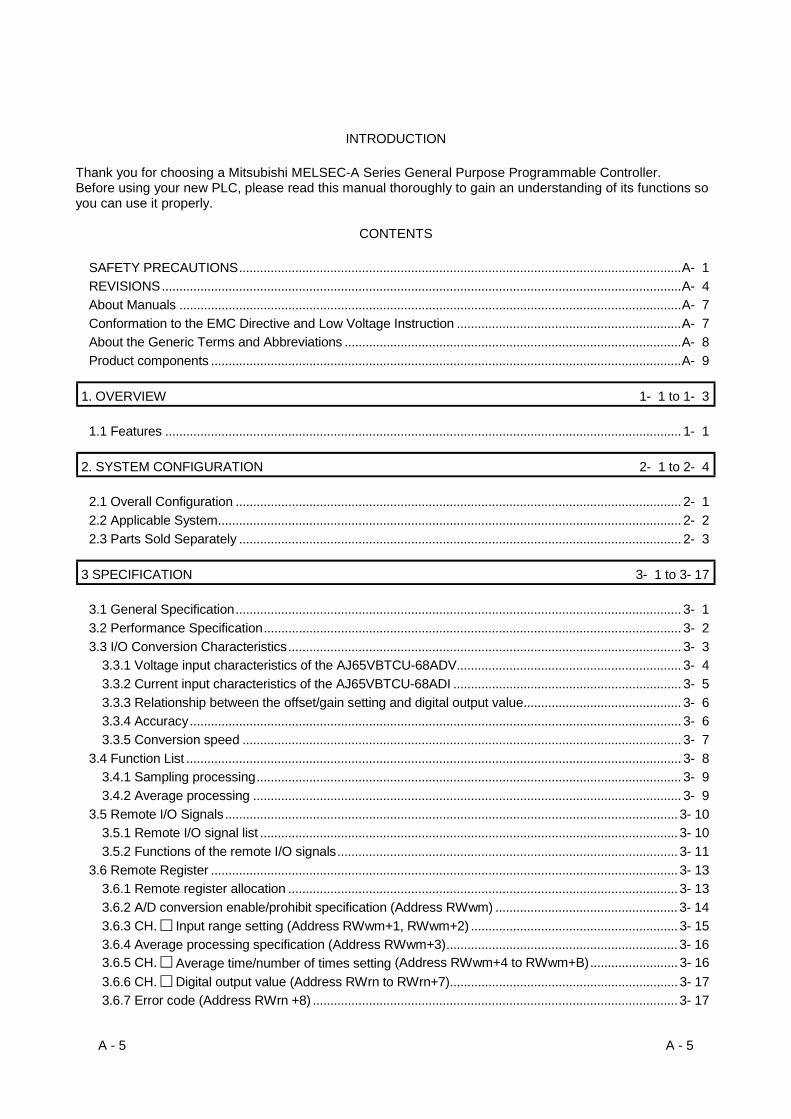
CONTENTS
SAFETY PRECAUTIONS..............................................................................................................................A- 1REVISIONS....................................................................................................................................................A- 4About Manuals ...............................................................................................................................................A- 7Conformation to the EMC Directive and Low Voltage Instruction ................................................................A- 7About the Generic Terms and Abbreviations ................................................................................................A- 8Product components ......................................................................................................................................A- 9
1. OVERVIEW 1- 1 to 1- 3
1.1 Features ................................................................................................................................................... 1- 1
2. SYSTEM CONFIGURATION 2- 1 to 2- 4
2.1 Overall Configuration ............................................................................................................................... 2- 12.2 Applicable System.................................................................................................................................... 2- 22.3 Parts Sold Separately .............................................................................................................................. 2- 3
3 SPECIFICATION 3- 1 to 3- 17
3.1 General Specification............................................................................................................................... 3- 13.2 Performance Specification....................................................................................................................... 3- 23.3 I/O Conversion Characteristics................................................................................................................ 3- 3
3.3.1 Voltage input characteristics of the AJ65VBTCU-68ADV................................................................ 3- 43.3.2 Current input characteristics of the AJ65VBTCU-68ADI ................................................................. 3- 53.3.3 Relationship between the offset/gain setting and digital output value............................................. 3- 63.3.4 Accuracy............................................................................................................................................ 3- 63.3.5 Conversion speed ............................................................................................................................. 3- 7
3.4 Function List ............................................................................................................................................. 3- 83.4.1 Sampling processing......................................................................................................................... 3- 93.4.2 Average processing .......................................................................................................................... 3- 9
3.5 Remote I/O Signals................................................................................................................................. 3- 103.5.1 Remote I/O signal list ....................................................................................................................... 3- 103.5.2 Functions of the remote I/O signals................................................................................................. 3- 11
3.6 Remote Register ..................................................................................................................................... 3- 133.6.1 Remote register allocation ............................................................................................................... 3- 133.6.2 A/D conversion enable/prohibit specification (Address RWwm) .................................................... 3- 143.6.3 CH. Input range setting (Address RWwm+1, RWwm+2) ........................................................... 3- 153.6.4 Average processing specification (Address RWwm+3).................................................................. 3- 163.6.5 CH. Average time/number of times setting (Address RWwm+4 to RWwm+B)......................... 3- 163.6.6 CH. Digital output value (Address RWrn to RWrn+7)................................................................. 3- 173.6.7 Error code (Address RWrn +8) ........................................................................................................ 3- 17

A - 6 A - 6
4 SETUP AND PREPARATION BEFORE OPERATION 4- 1 to 4- 15
4.1 Pre-Operation Procedure......................................................................................................................... 4- 14.2 Precautions When Handling .................................................................................................................... 4- 14.3 Name of Each Part................................................................................................................................... 4- 34.4 Offset/Gain Setting................................................................................................................................... 4- 64.5 Station Number Setting............................................................................................................................ 4- 84.6 Facing Direction of the Module Installation ............................................................................................. 4- 84.7 Data Link Cable Wiring ............................................................................................................................ 4- 9
4.7.1 Instructions for handling the CC-Link dedicated cables................................................................... 4- 94.7.2 Connection of the CC-Link dedicated cables.................................................................................. 4- 10
4.8 Wiring....................................................................................................................................................... 4- 114.8.1 Wiring precautions............................................................................................................................ 4- 114.8.2 Wiring of module with external equipment ...................................................................................... 4- 12
4.9 How to Wire the One-Touch Connector Plug......................................................................................... 4- 134.10 Maintenance and Inspection................................................................................................................. 4- 15
5 PROGRAMMING 5- 1 to 5- 13
5.1 Programming Procedure.......................................................................................................................... 5- 15.2 Conditions of Program Examples............................................................................................................ 5- 25.3 Program Example for Use of the QCPU (Q mode)................................................................................. 5- 45.4 Program Example for Use of the QnACPU............................................................................................. 5- 75.5 Program Example for Use of the ACPU/QCPU (A mode) (dedicated instructions) .............................. 5- 95.6 Program Example for Use of the ACPU/QCPU (A mode) (FROM/TO instructions) ............................ 5- 12
6 TROUBLESHOOTING 6- 1 to 6- 6
6.1 Error Code List ......................................................................................................................................... 6- 16.2 Using the LED Indications to Check Errors............................................................................................. 6- 26.3 When the digital output value cannot be read......................................................................................... 6- 46.4 Troubleshooting for the Case where the "ERR." LED of the Master Station Flickers ........................... 6- 5
APPENDIX App- 1 to App- 4
Appendix1 Comparison between This Product andAJ65SBT-64AD .......................................................App- 1Appendix2 External dimension diagram....................................................................................................App- 3
INDEX Index- 1 to Index- 2
A - 7 A - 7
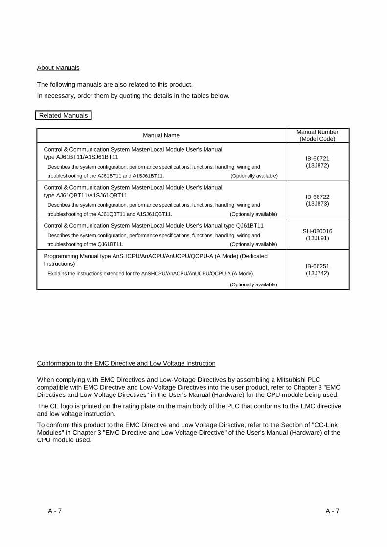
About Manuals
The following manuals are also related to this product.
In necessary, order them by quoting the details in the tables below.
Related Manuals
Manual Name Manual Number(Model Code)
Control & Communication System Master/Local Module User's Manualtype AJ61BT11/A1SJ61BT11
Describes the system configuration, performance specifications, functions, handling, wiring and
troubleshooting of the AJ61BT11 and A1SJ61BT11. (Optionally available)
IB-66721(13J872)
Control & Communication System Master/Local Module User's Manualtype AJ61QBT11/A1SJ61QBT11
Describes the system configuration, performance specifications, functions, handling, wiring and
troubleshooting of the AJ61QBT11 and A1SJ61QBT11. (Optionally available)
IB-66722(13J873)
Control & Communication System Master/Local Module User's Manual type QJ61BT11Describes the system configuration, performance specifications, functions, handling, wiring and
troubleshooting of the QJ61BT11. (Optionally available)
SH-080016(13JL91)
Programming Manual type AnSHCPU/AnACPU/AnUCPU/QCPU-A (A Mode) (DedicatedInstructions)
Explains the instructions extended for the AnSHCPU/AnACPU/AnUCPU/QCPU-A (A Mode).
(Optionally available)
IB-66251(13J742)
Conformation to the EMC Directive and Low Voltage Instruction
When complying with EMC Directives and Low-Voltage Directives by assembling a Mitsubishi PLCcompatible with EMC Directive and Low-Voltage Directives into the user product, refer to Chapter 3 "EMCDirectives and Low-Voltage Directives" in the User’s Manual (Hardware) for the CPU module being used.
The CE logo is printed on the rating plate on the main body of the PLC that conforms to the EMC directiveand low voltage instruction.
To conform this product to the EMC Directive and Low Voltage Directive, refer to the Section of "CC-LinkModules" in Chapter 3 "EMC Directive and Low Voltage Directive" of the User's Manual (Hardware) of theCPU module used.

A - 8 A - 8
About the Generic Terms and Abbreviations
Unless otherwise specified, the following generic terms and abbreviations are used in this manual todescribe Type AJ65VBTCU-68ADV/ADI analog-digital converter module.
Generic Term/Abbreviation Description
GX DeveloperGeneric product name of the product types SWnD5C-GPPW-E, SWnD5C-GPPW-EA,SWnD5C-GPPW-EV and SWnD5C-GPPW-EVA(n in the type indicates 4 or more.)
ACPU
Generic term for A0J2CPU, A0J2HCPU, A2CPU, A2CPU-S1, A3CPU, A1SCPU,A1SCPU-S1, A1SCPUC-24-R2, A1SHCPU, A1SJCPU, A1SJCPU-S3, A1SJHCPU,A1NCPU, A2NCPU, A2NCPU-S1, A3NCPU, A3MCPU, A3HCPU, A2SCPU,A2SCPU-S1, A2SHCPU, A2SHCPU-S1, A2ACPU, A2ACPU-S1, A3ACPU, A2UCPU,A2UCPU-S1, A2ASCPU, A2ASCPU-S1, A2ASCPU-S30, A2USHCPU-S1, A3UCPU,A4UCPU
QnACPU Generic term for Q2ACPU, Q2ACPU-S1, Q2ASCPU, Q2ASCPU-S1, Q2ASHCPU,Q2ASHCPU-S1, Q3ACPU, Q4ACPU, Q4ARCPU
QCPU (A mode) Generic term for Q02CPU-A, Q02HCPU-A, Q06HCPU-A
QCPU (Q mode) Generic term for Q00JCPU, Q00CPU, Q01CPU, Q02CPU, Q02HCPU, Q06HCPU,Q12HCPU, Q25HCPU
Master station Station that controls the data link system.One master station is required for each system.
Local station Station having a PLC CPU and the ability to communicate with the master and otherlocal stations.
Remote I/O station Remote station that handles bit unit data only. (Performs input and output withexternal devices.) (AJ65BTB1-16D, AJ65SBTB1-16D)
Remote device station Remote station that handles bit unit and word unit data only. (Performs input andoutput with external devices, and analog data exchange.)
Remote station Generic term for remote I/O station and remote device station.(Controlled by the master station)
Intelligent device station Station that can perform transient transmission, such as the AJ65BT-R2 (includinglocal stations).
Master module Generic term for QJ61BT11, AJ61BT11, A1SJ61BT11, AJ61QBT11, andA1SJ61QBT11 when they are used as master stations.
SBLink special relay (for CC-Link)Bit unit information that indicates the module operating status and data link status ofthe master station/local station. (Expressed as SB for convenience)
SWLink special register (for CC-Link)16 bit unit information that indicates the module operating status and data link statusof the master station/local station. (Expressed as SW for convenience)
RXRemote input (for CC-Link)Information entered in bit units from the remote station to the master station.(Expressed as RX for convenience)
RYRemote output (for CC-Link)Information output in bit units from the master station to the remote station.(Expressed as RY for convenience)
RWwRemote register (Write area for CC-Link)Information output in 16-bit units from the master station to the remote device station.(Expressed as RWw for convenience)
RWr
Remote register (Read area for CC-Link)Information entered in 16-bit units from the remote device station to the masterstation.(Expressed as RWr for convenience)
A - 9 A - 9
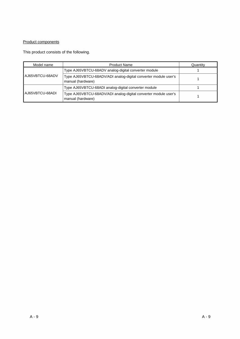
Product components
This product consists of the following.
Model name Product Name QuantityType AJ65VBTCU-68ADV analog-digital converter module 1
AJ65VBTCU-68ADV Type AJ65VBTCU-68ADV/ADI analog-digital converter module user'smanual (hardware) 1
Type AJ65VBTCU-68ADI analog-digital converter module 1AJ65VBTCU-68ADI Type AJ65VBTCU-68ADV/ADI analog-digital converter module user's
manual (hardware) 1
1 - 1 1 - 1
MELSEC-A1 OVERVIEW
1 OVERVIEW
This user's manual explains the specifications, handling, programming methods andothers of Type AJ65VBTCU-68ADV analog-digital converter module (hereafterabbreviated to the " AJ65VBTCU-68ADV") and Type AJ65VBTCU-68ADI analog-digital converter module (hereafter abbreviated to the “AJ65VBTCU-68ADI”) which isused as a remote device station of a Control & Communication Link (hereafterabbreviated to "CC-Link") system.In this manual, the AJ65VBTCU-68ADV and AJ65VBTCU-68ADI are genericallyreferred to as the AJ65VBTCU-68ADV/ADI.The AJ65VBTCU-68ADV/ADI converts the analog signals (voltage or current input)from the PLC's external source to a 16-bit encoded binary data digital value.
1.1 Features
This section gives the features of the AJ65VBTCU-68ADV/ADI.
(1) Selection of model according to applicationAJ65VBTCU-68ADV......Voltage input on all eight channels.AJ65VBTCU-68ADI .......Current input on all eight channels.
(2) High accuracyThis module performs A/D conversion at the accuracy of ±0.3% relative to themaximum value of the digital output value at the operating ambient temperatureof 0 to 55°C, or at ±0.2% relative to the maximum value of the digital output valueat the operating ambient temperature of 25±5°C.
(3) Input range selectable per channelYou can choose the analog input range per channel to change the I/O conversioncharacteristics.
(4) High resolution of 1/±4000By changing the input range, you can choose and set the digital value resolutionto either 1/4000 or 1/±4000 (Only AJ65VBTCU-68ADV) to provide high-resolutiondigital values.
(5) Designation of sampling processing or average processingAs a conversion method, you can specify sampling processing or averageprocessing per channel.
(6) More channels than those of the conventional A/D convertermodulesThe number of channels is twice greater than that of the conventional CC-LinkA/D converter module (AJ65SBT-64AD).
1
1 - 2 1 - 2
MELSEC-A1 OVERVIEW
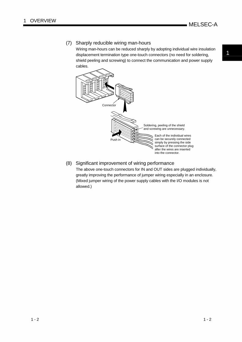
(7) Sharply reducible wiring man-hoursWiring man-hours can be reduced sharply by adopting individual wire insulationdisplacement termination type one-touch connectors (no need for soldering,shield peeling and screwing) to connect the communication and power supplycables.
Connector
Soldering, peeling of the shield and screwing are unnecessary.
Push inEach of the individual wires can be securely connected simply by pressing the side surface of the connector plug after the wires are inserted into the connector.
(8) Significant improvement of wiring performanceThe above one-touch connectors for IN and OUT sides are plugged individually,greatly improving the performance of jumper wiring especially in an enclosure.(Mixed jumper wiring of the power supply cables with the I/O modules is notallowed.)
1
1 - 3 1 - 3
MELSEC-A1 OVERVIEW
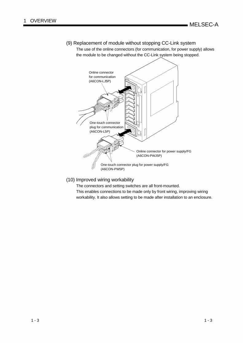
(9) Replacement of module without stopping CC-Link systemThe use of the online connectors (for communication, for power supply) allowsthe module to be changed without the CC-Link system being stopped.
One-touch connectorplug for communication(A6CON-L5P)
One-touch connector plug for power supply/FG(A6CON-PW5P)
Online connector for power supply/FG(A6CON-PWJ5P)
Online connectorfor communication(A6CON-LJ5P)
(10) Improved wiring workabilityThe connectors and setting switches are all front-mounted.This enables connections to be made only by front wiring, improving wiringworkability. It also allows setting to be made after installation to an enclosure.
2 - 1 2 - 1
MELSEC-A2 SYSTEM CONFIGURATION
2 SYSTEM CONFIGURATION
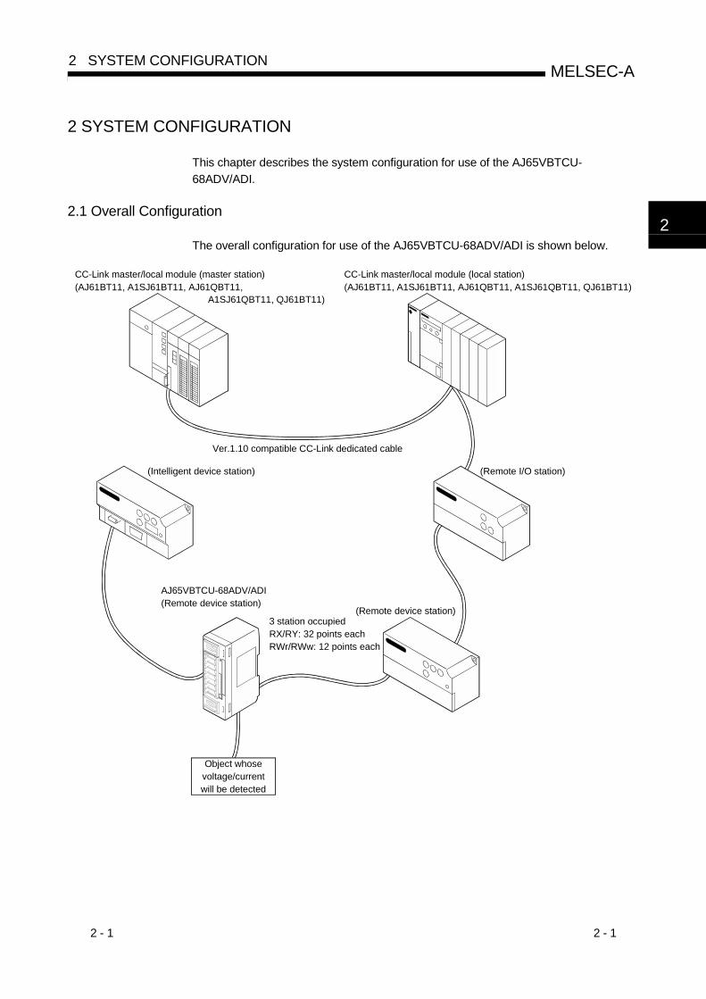
This chapter describes the system configuration for use of the AJ65VBTCU-68ADV/ADI.
2.1 Overall Configuration
The overall configuration for use of the AJ65VBTCU-68ADV/ADI is shown below.
CC-Link master/local module (local station)(AJ61BT11, A1SJ61BT11, AJ61QBT11, A1SJ61QBT11, QJ61BT11)
Ver.1.10 compatible CC-Link dedicated cable
(Intelligent device station) (Remote I/O station)
(Remote device station)
AJ65VBTCU-68ADV/ADI(Remote device station)
3 station occupiedRX/RY: 32 points eachRWr/RWw: 12 points each
Object whosevoltage/currentwill be detected
CC-Link master/local module (master station)(AJ61BT11, A1SJ61BT11, AJ61QBT11,
A1SJ61QBT11, QJ61BT11)
2
2 - 2 2 - 2
MELSEC-A2 SYSTEM CONFIGURATION
2.2 Applicable System
This section explains the applicable system.
(1) Applicable master modulesThe following master modules can be used with the AJ65VBTCU-68ADV/ADI. AJ61BT11 A1SJ61BT11 AJ61QBT11 A1SJ61QBT11 QJ61BT11
(2) Restrictions on use of CC-Link dedicated instructions (RLPA,RRPA)The CC-Link dedicated instructions may not be used depending on the PLC CPUand master module used.For details of the restrictions, refer to the A series master module user's manual,and the Programing Manual type AnSHCPU/AnACPU/AnUCPU/QCPU (A mode)(Dedicated Instructions).This module does not allow the use of the dedicated instructions other thanRLPA and RRPA.Refer to Section 5.5 for a program example using the dedicated instructions(RLPA, RRPA).
2

2 - 3 2 - 3
MELSEC-A2 SYSTEM CONFIGURATION
2.3 Parts Sold Separately
The plugs for AJ65VBTCU-68ADV/ADI are sold separately.Please purchase them as necessary.
Mitsubishi modelname
Part model name(manufacturer)
Specifications Color ofthe cover
Applicable cable core size(mm2)
Applicable cableouter diameter
(mm)
Maximumrated
current (A)
A6CON-P21433104-6000FL
(3M) 1.0 to 1.4 Transparent
A6CON-P22033104-6100FL
(3M)
0.14 to 0.2(AWG#26 to 24)
1.4 to 2.02
Yellow
A6CON-P51433104-6200FL
(3M) 1.0 to 1.4 Red
Plug forone-touch connector
1, 4
A6CON-P52033104-6300FL
(3M)
0.3 to 0.5(AWG#22 to 20)
1.4 to 2.03
Blue
communication line0.5 (AWG#20) 2.2 to 3.0
One-touchconnector plug for
communication 2, 4
A6CON-L5P 35505-6000-BOM GF (3M) shielded cable (drain wire)
0.5 (AWG#20)
Red
One-touchconnector for powersupply/FG 2, 4
A6CON-PW5P 35505-6080-A00GF (3M)
0.75 (0.66 to 0.98) (AWG#18)wire diameter 0.16 mm or
more 2.2 to 3.0 7 Gray
Online connector forcommunication 3 A6CON-LJ5P
35720-L200-B00AK (3M)
Online connector forpower supply/FG 3
A6CON-PWJ5P35720-L200-A00
AK (3M)
One-touch connectorplug with terminating
resistor(including 1)
A6CON-TR11 One-touch connector plug withterminating resister attachedfor communication (110Ω)
1 Mitsubishi's A6CON-P includes 20 plugs.2 Mitsubishi's A6CON- 5P includes 10 plugs.3 Mitsubishi's A6CON- J5P includes 5 plugs.4 Once insulation-displaced, the one-touch connector plugs cannot be reused.
2 - 4 2 - 4
MELSEC-A2 SYSTEM CONFIGURATION
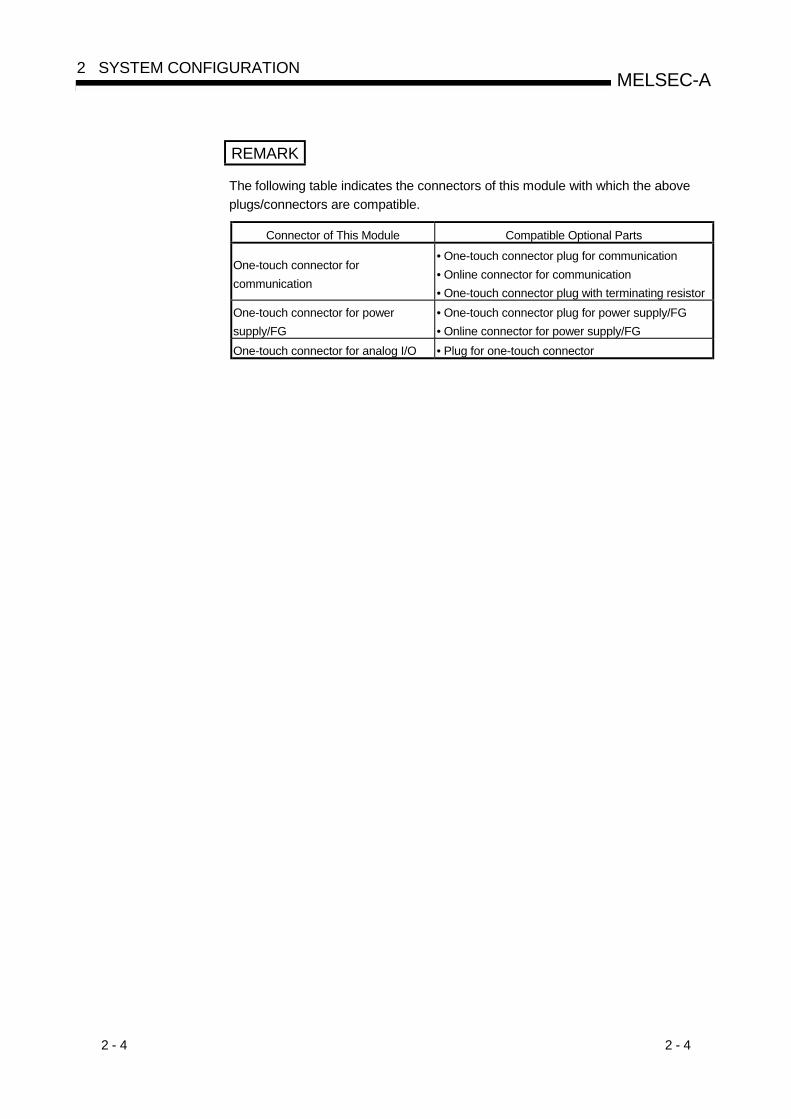
REMARK
The following table indicates the connectors of this module with which the aboveplugs/connectors are compatible.
Connector of This Module Compatible Optional Parts
One-touch connector forcommunication
• One-touch connector plug for communication• Online connector for communication• One-touch connector plug with terminating resistor
One-touch connector for powersupply/FG
• One-touch connector plug for power supply/FG• Online connector for power supply/FG
One-touch connector for analog I/O • Plug for one-touch connector
3 - 1 3 - 1
MELSEC-A3 SPECIFICATION
3 SPECIFICATION
This chapter provides the specifications of the AJ65VBTCU-68ADV/ADI.
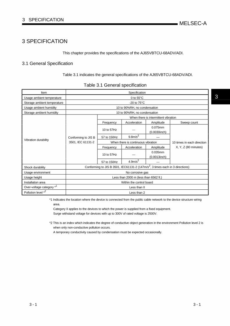
3.1 General Specification
Table 3.1 indicates the general specifications of the AJ65VBTCU-68ADV/ADI.
Table 3.1 General specificationItem Specification
Usage ambient temperature 0 to 55°CStorage ambient temperature -20 to 75°CUsage ambient humidity 10 to 90%RH, no condensationStorage ambient humidity 10 to 90%RH, no condensation
When there is intermittent vibrationFrequency Acceleration Amplitude Sweep count
10 to 57Hz —0.075mm
(0.0030inch)57 to 150Hz 9.8m/s2 —
When there is continuous vibrationFrequency Acceleration Amplitude
10 to 57Hz —0.035mm
(0.0013inch)
Vibration durabilityConforming to JIS B3501, IEC 61131-2
57 to 150Hz 4.9m/s2 —
10 times in each directionX, Y, Z (80 minutes)
Shock durability Conforming to JIS B 3501, IEC61131-2 (147m/s2, 3 times each in 3 directions)
Usage environment No corrosive gasUsage height Less than 2000 m (less than 6562 ft.)Installation area Within the control boardOver-voltage category *1 Less than IIPollution level *2 Less than 2
*1 Indicates the location where the device is connected from the public cable network to the device structure wiringarea.Category II applies to the devices to which the power is supplied from a fixed equipment.Surge withstand voltage for devices with up to 300V of rated voltage is 2500V.
*2 This is an index which indicates the degree of conductive object generation in the environment Pollution level 2 iswhen only non-conductive pollution occurs.A temporary conductivity caused by condensation must be expected occasionally.
3
3 - 2 3 - 2
MELSEC-A3 SPECIFICATION
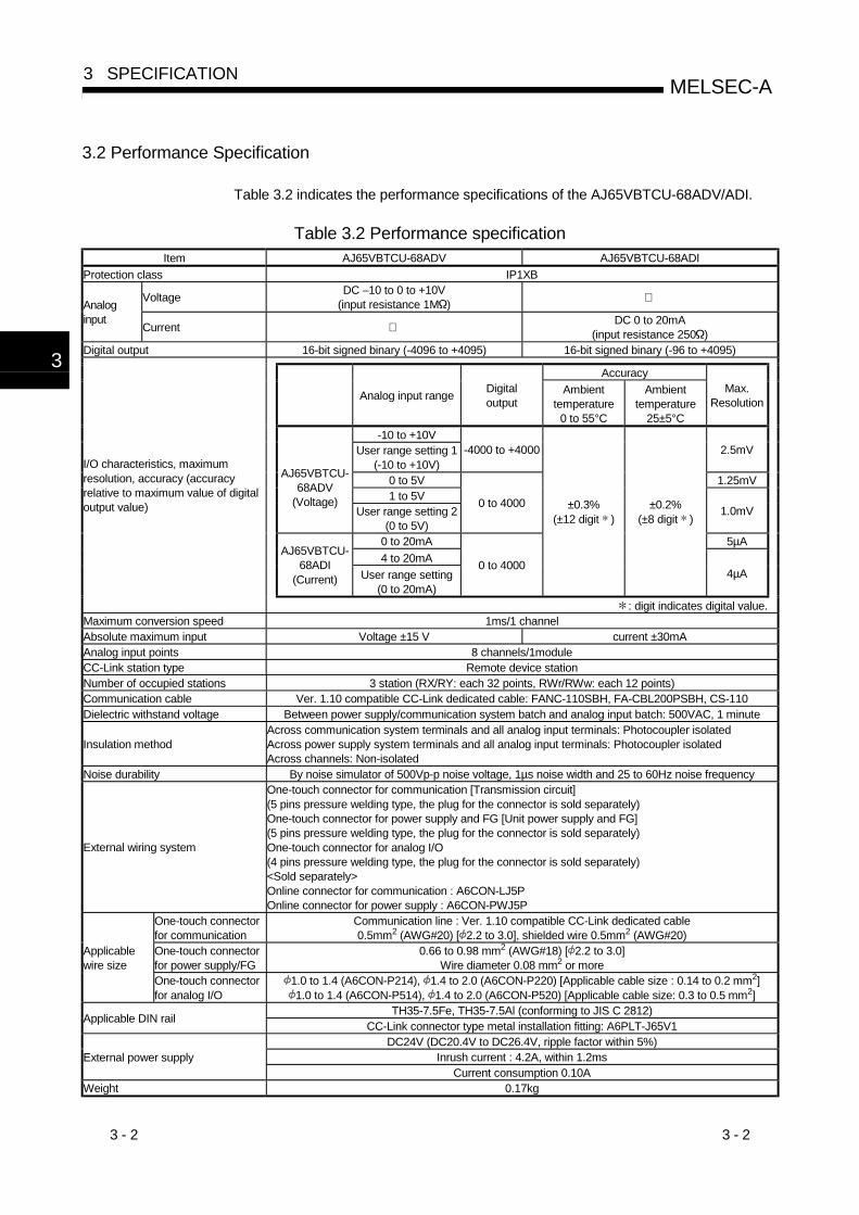
3.2 Performance Specification
Table 3.2 indicates the performance specifications of the AJ65VBTCU-68ADV/ADI.
Table 3.2 Performance specificationItem AJ65VBTCU-68ADV AJ65VBTCU-68ADI
Protection class IP1XB
Voltage DC –10 to 0 to +10V(input resistance 1M ) Analog
inputCurrent DC 0 to 20mA
(input resistance 250 )Digital output 16-bit signed binary (-4096 to +4095) 16-bit signed binary (-96 to +4095)
Accuracy
Analog input range Digitaloutput
Ambienttemperature
0 to 55°C
Ambienttemperature
25±5°C
Max.Resolution
-10 to +10VUser range setting 1
(-10 to +10V)-4000 to +4000 2.5mV
0 to 5V 1.25mV1 to 5V
AJ65VBTCU-68ADV
(Voltage)User range setting 2
(0 to 5V)
0 to 40001.0mV
0 to 20mA 5µA4 to 20mAAJ65VBTCU-
68ADI(Current) User range setting
(0 to 20mA)
0 to 4000
±0.3%(±12 digit )
±0.2%(±8 digit )
4µA
I/O characteristics, maximumresolution, accuracy (accuracyrelative to maximum value of digitaloutput value)
: digit indicates digital value.Maximum conversion speed 1ms/1 channelAbsolute maximum input Voltage ±15 V current ±30mAAnalog input points 8 channels/1moduleCC-Link station type Remote device stationNumber of occupied stations 3 station (RX/RY: each 32 points, RWr/RWw: each 12 points)Communication cable Ver. 1.10 compatible CC-Link dedicated cable: FANC-110SBH, FA-CBL200PSBH, CS-110Dielectric withstand voltage Between power supply/communication system batch and analog input batch: 500VAC, 1 minute
Insulation methodAcross communication system terminals and all analog input terminals: Photocoupler isolatedAcross power supply system terminals and all analog input terminals: Photocoupler isolatedAcross channels: Non-isolated
Noise durability By noise simulator of 500Vp-p noise voltage, 1µs noise width and 25 to 60Hz noise frequency
External wiring system
One-touch connector for communication [Transmission circuit](5 pins pressure welding type, the plug for the connector is sold separately)One-touch connector for power supply and FG [Unit power supply and FG](5 pins pressure welding type, the plug for the connector is sold separately)One-touch connector for analog I/O(4 pins pressure welding type, the plug for the connector is sold separately)<Sold separately>Online connector for communication : A6CON-LJ5POnline connector for power supply : A6CON-PWJ5P
One-touch connectorfor communication
Communication line : Ver. 1.10 compatible CC-Link dedicated cable0.5mm2 (AWG#20) [ 2.2 to 3.0], shielded wire 0.5mm2 (AWG#20)
One-touch connectorfor power supply/FG
0.66 to 0.98 mm2 (AWG#18) [ 2.2 to 3.0]Wire diameter 0.08 mm2 or more
Applicablewire size
One-touch connectorfor analog I/O
1.0 to 1.4 (A6CON-P214), 1.4 to 2.0 (A6CON-P220) [Applicable cable size : 0.14 to 0.2 mm2]1.0 to 1.4 (A6CON-P514), 1.4 to 2.0 (A6CON-P520) [Applicable cable size: 0.3 to 0.5 mm2]
TH35-7.5Fe, TH35-7.5Al (conforming to JIS C 2812)Applicable DIN rail CC-Link connector type metal installation fitting: A6PLT-J65V1DC24V (DC20.4V to DC26.4V, ripple factor within 5%)
Inrush current : 4.2A, within 1.2msExternal power supplyCurrent consumption 0.10A
Weight 0.17kg
3

3 - 3 3 - 3
MELSEC-A3 SPECIFICATION
3.3 I/O Conversion Characteristics
The I/O characteristics is the slope created by connecting the offset and gain values,with a straight line when converting the analog signals (voltage or current input) froman external source of the PLC to digital values.The offset value is an analog input value (voltage or current) at which the digital outputvalue is 0.The gain value is an analog input value (voltage or current) at which the digital outputvalue is 4000.
3 - 4 3 - 4
MELSEC-A3 SPECIFICATION
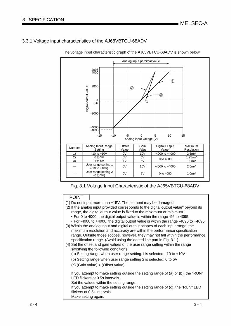
3.3.1 Voltage input characteristics of the AJ68VBTCU-68ADV
The voltage input characteristic graph of the AJ65VBTCU-68ADV is shown below.
3
2
1
40954000
2000
-2000
-4000-4096
0 1
-15 -10 -5 0 5 10 15Analog input voltage (V)
Analog input parcitcal value
-96
Dig
ital o
utpu
t val
ue
Number Analog Input RangeSetting
OffsetValue
GainValue
Digital OutputValue*
MaximumResolution
1) -10 to +10V 0V 10V -4000 to +4000 2.5mV2) 0 to 5V 0V 5V 1.25mV3) 1 to 5V 1V 5V 0 to 4000 1.0mV
— User range setting 1(-10 to +10V) 0V 10V -4000 to +4000 2.5mV
— User range setting 2(0 to 5V) 0V 5V 0 to 4000 1.0mV
Fig. 3.1 Voltage Input Characteristic of the AJ65VBTCU-68ADV
POINT(1) Do not input more than ±15V. The element may be damaged.(2) If the analog input provided corresponds to the digital output value* beyond its
range, the digital output value is fixed to the maximum or minimum. For 0 to 4000, the digital output value is within the range -96 to 4095. For -4000 to +4000, the digital output value is within the range -4096 to +4095.
(3) Within the analog input and digital output scopes of each input range, themaximum resolution and accuracy are within the performance specificationrange. Outside those scopes, however, they may not fall within the performancespecification range. (Avoid using the dotted line part in Fig. 3.1.)
(4) Set the offset and gain values of the user range setting within the rangesatisfying the following conditions.(a) Setting range when user range setting 1 is selected: -10 to +10V(b) Setting range when user range setting 2 is selected: 0 to 5V(c) (Gain value) > (Offset value)
If you attempt to make setting outside the setting range of (a) or (b), the "RUN"LED flickers at 0.5s intervals.Set the values within the setting range.If you attempt to make setting outside the setting range of (c), the "RUN" LEDflickers at 0.5s intervals.Make setting again.
3 - 5 3 - 5
MELSEC-A3 SPECIFICATION
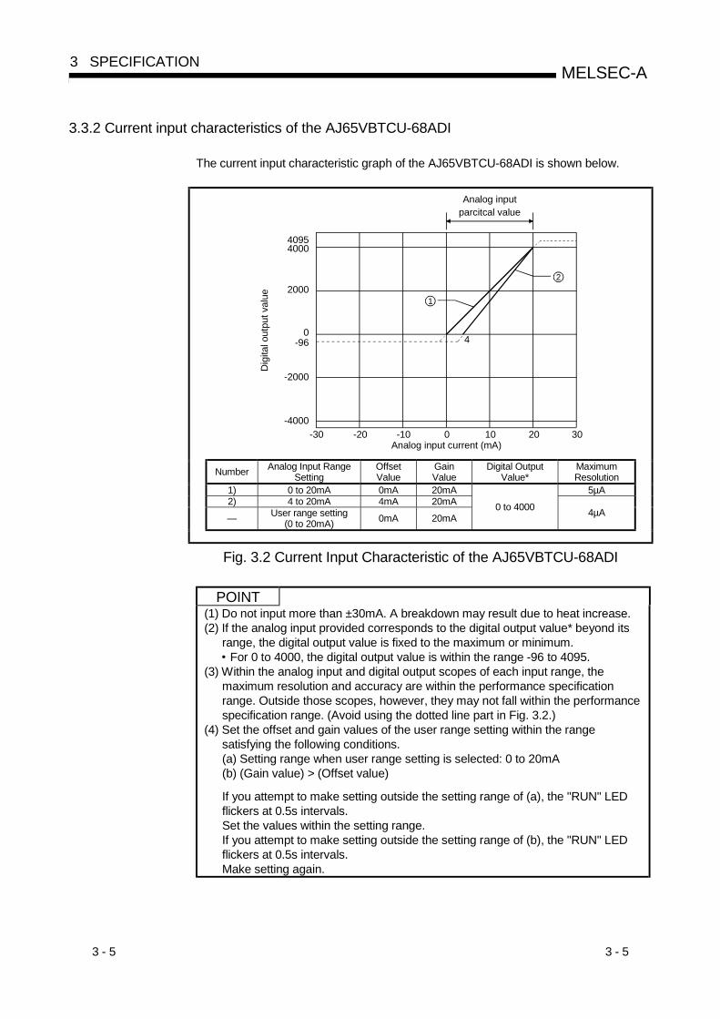
3.3.2 Current input characteristics of the AJ65VBTCU-68ADI
The current input characteristic graph of the AJ65VBTCU-68ADI is shown below.
2
1
40954000
2000
-2000
-4000
04
-30 -20 -10 0 10 20 30Analog input current (mA)
Analog input parcitcal value
-96
Dig
ital o
utpu
t val
ue
Number Analog Input RangeSetting
OffsetValue
GainValue
Digital OutputValue*
MaximumResolution
1) 0 to 20mA 0mA 20mA 5µA2) 4 to 20mA 4mA 20mA
— User range setting(0 to 20mA) 0mA 20mA
0 to 4000 4µA
Fig. 3.2 Current Input Characteristic of the AJ65VBTCU-68ADI
POINT(1) Do not input more than ±30mA. A breakdown may result due to heat increase.(2) If the analog input provided corresponds to the digital output value* beyond its
range, the digital output value is fixed to the maximum or minimum. For 0 to 4000, the digital output value is within the range -96 to 4095.
(3) Within the analog input and digital output scopes of each input range, themaximum resolution and accuracy are within the performance specificationrange. Outside those scopes, however, they may not fall within the performancespecification range. (Avoid using the dotted line part in Fig. 3.2.)
(4) Set the offset and gain values of the user range setting within the rangesatisfying the following conditions.(a) Setting range when user range setting is selected: 0 to 20mA(b) (Gain value) > (Offset value)
If you attempt to make setting outside the setting range of (a), the "RUN" LEDflickers at 0.5s intervals.Set the values within the setting range.If you attempt to make setting outside the setting range of (b), the "RUN" LEDflickers at 0.5s intervals.Make setting again.
3 - 6 3 - 6
MELSEC-A3 SPECIFICATION
3.3.3 Relationship between the offset/gain setting and digital output value
The relationship between the offset/gain setting and digital output value is described.
(1) ResolutionThe resolution is obtained by the following formula:(a) For the AJ65VBTCU-68ADV:
(Gain value) - (Offset value)Resolution = 4000
(b) For the AJ65VBTCU-68ADI:
(Gain value) - (Offset value)Resolution = 4000
(2) Relationship between the maximum resolution and digital outputvalueThe maximum resolution of the AJ65VBTCU-68ADV/ADI is as indicated in theperformance specification.If the following is satisfied from the offset/gain setting, the digital output valuedoes not increases /decreases by one.
(Gain value) - (Offset value)4000 < Maximum resolution
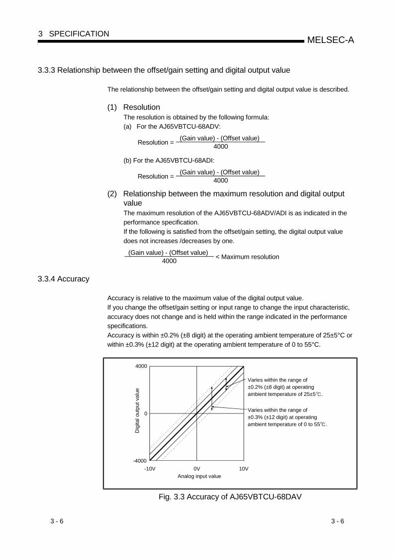
3.3.4 Accuracy
Accuracy is relative to the maximum value of the digital output value.If you change the offset/gain setting or input range to change the input characteristic,accuracy does not change and is held within the range indicated in the performancespecifications.Accuracy is within ±0.2% (±8 digit) at the operating ambient temperature of 25±5°C orwithin ±0.3% (±12 digit) at the operating ambient temperature of 0 to 55°C.
4000
-10V 10V-4000
0V
Dig
ital o
utpu
t val
ue
Analog input value
Varies within the range of±0.2% (±8 digit) at operatingambient temperature of 25±5 .
Varies within the range of±0.3% (±12 digit) at operatingambient temperature of 0 to 55 .
0
Fig. 3.3 Accuracy of AJ65VBTCU-68DAV
3 - 7 3 - 7
MELSEC-A3 SPECIFICATION
4000
0 20mA0
Varies within the range of±0.2% (±8 digit) at operatingambient temperature of 25±5 .
Varies within the range of±0.3% (±12 digit) at operatingambient temperature of 0 to 55 .
Dig
ital o
utpu
t val
ue
Analog input value
Fig. 3.4 Accuracy of AJ65VBTCU-68DAI
3.3.5 Conversion speed
Conversion speed indicates time from channel changing to A/D conversion completion.Conversion speed per channel of the AJ65VBTCU-68ADV/ADI is 1ms.Due to the data link processing time of the CC-Link system, there is a transmissiondelay until the A/D conversion value is read actually.For the data link processing time, refer to the user's manual of the master moduleused.
Example) Data link processing time taken in the asynchronous mode when the mastermodule is the QJ61BT11 (normal value)
[Calculation expression]SM+LS×1+remote device station processing time
SM : Scan time of master station sequence programLS : Link scan timeRemote device station processing time: (Number of channels used+1 )
× 1ms: Internal processing time of AJ65VBTCU-68ADV/ADI
3 - 8 3 - 8
MELSEC-A3 SPECIFICATION
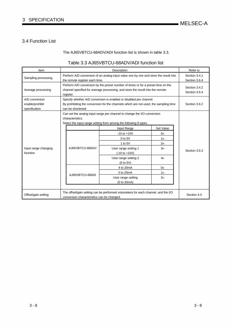
3.4 Function List
The AJ65VBTCU-68ADV/ADI function list is shown in table 3.3.
Table 3.3 AJ65VBTCU-68ADV/ADI function listItem Description Refer to
Sampling processingPerform A/D conversion of an analog input value one by one and store the result intothe remote register each time.
Section 3.4.1Section 3.6.4
Average processingPerform A/D conversion by the preset number of times or for a preset time on thechannel specified for average processing, and store the result into the remoteregister.
Section 3.4.2Section 3.6.4
A/D conversionenable/prohibitspecification
Specify whether A/D conversion is enabled or disabled per channel.By prohibiting the conversion for the channels which are not used, the sampling timecan be shortened.
Section 3.6.2
Can set the analog input range per channel to change the I/O conversioncharacteristics.Select the input range setting from among the following 8 types.
Input Range Set Value-10 to +10V 0H
0 to 5V 1H
1 to 5V 2H
User range setting 1(-10 to +10V)
3HAJ65VBTCU-68ADV
User range setting 2(0 to 5V)
4H
4 to 20mA 0H
0 to 20mA 1HAJ65VBTCU-68ADI
User range setting(0 to 20mA)
2H
Input range changingfunction
Section 3.6.3
Offset/gain settingThe offset/gain setting can be performed volumeless for each channel, and the I/Oconversion characteristics can be changed.
Section 4.4
3 - 9 3 - 9
MELSEC-A3 SPECIFICATION
3.4.1 Sampling processing
The A/D conversion is performed successively for the analog input, and the converteddigital output values are stored in the remote register.The processing time to store the digital output value into the remote register after thesampling processing differs depending on the number of A/D conversion enabledchannels.
(Processing time) Number of A/D conversion enabled channels) 1 (ms)
Maximum conversion speed
[Example] When three channels, channels 1, 2, and 3 are enabled for conversion:3×1 = 3 (ms)
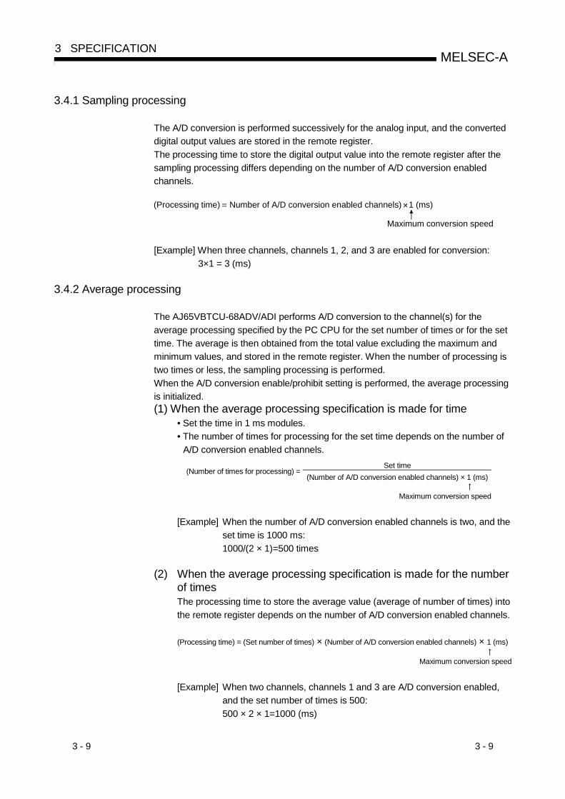
3.4.2 Average processing
The AJ65VBTCU-68ADV/ADI performs A/D conversion to the channel(s) for theaverage processing specified by the PC CPU for the set number of times or for the settime. The average is then obtained from the total value excluding the maximum andminimum values, and stored in the remote register. When the number of processing istwo times or less, the sampling processing is performed.When the A/D conversion enable/prohibit setting is performed, the average processingis initialized.(1) When the average processing specification is made for time
• Set the time in 1 ms modules.• The number of times for processing for the set time depends on the number of
A/D conversion enabled channels.Set time
(Number of times for processing) =(Number of A/D conversion enabled channels) × 1 (ms)
Maximum conversion speed
[Example] When the number of A/D conversion enabled channels is two, and theset time is 1000 ms:1000/(2 × 1)=500 times
(2) When the average processing specification is made for the numberof timesThe processing time to store the average value (average of number of times) intothe remote register depends on the number of A/D conversion enabled channels.
(Processing time) = (Set number of times) × (Number of A/D conversion enabled channels) × 1 (ms)
Maximum conversion speed
[Example] When two channels, channels 1 and 3 are A/D conversion enabled,and the set number of times is 500:500 × 2 × 1=1000 (ms)
3 - 10 3 - 10
MELSEC-A3 SPECIFICATION
3.5 Remote I/O Signals
This section describes the assignment and functions of the remote I/O signals.
3.5.1 Remote I/O signal list
Remote inputs (RX) mean the input signals from the AJ65VBTCU-68ADV/ADI to themaster module, and remote outputs (RY) mean the output signals from the mastermodule to the AJ65VBTCU-68ADV/ADI.In communications with the master station, the AJ65VBTCU-68ADV/ADI uses 32points of the remote inputs (RX) and 32 points of the remote outputs (RY).This module occupies three stations but do not use the latter 64 points.Table 3.4 indicates the assignment and names of the remote I/O signals.
Table 3.4 Remote I/O Signals ListSignal direction: AJ65VBTCU-68ADV/ADI Master Module Signal direction: Master Module AJ65VBTCU-68ADV/ADI
Remote input (RX) Signal name Remote output (RY) Signal nameRXn0 CH.1 A/D conversion completion flagRXn1 CH.2 A/D conversion completion flagRXn2 CH.3 A/D conversion completion flagRXn3 CH.4 A/D conversion completion flagRXn4 CH.5 A/D conversion completion flagRXn5 CH.6 A/D conversion completion flagRXn6 CH.7 A/D conversion completion flagRXn7 CH.8 A/D conversion completion flagRXn8
toRXnB
Reserved
RXnC E2PROM write error flag
RXnDto
RX(n+1)7Reserved
RYn0to
RY(n+1)7Reserved
RX(n+1)8 Initial data processing request flag RY(n+1)8 Initial data processing completion flagRX(n+1)9 Initial data setting completion flag RY(n+1)9 Initial data setting request flagRX(n+1)A Error status flag RY(n+1)A Error reset request flagRX(n+1)B Remote READYRX(n+1)C
toRX(n+1)F
Reserved
RY(n+1)8to
RY(n+1)FReserved
POINTThe reserved devices given in Table 3.4 are used by the system and cannot beused by the user.If the user has used (turned on/off) any of them, we cannot guarantee the functionsof the AJ65VBTCU-68ADV/ADI.
3 - 11 3 - 11
MELSEC-A3 SPECIFICATION
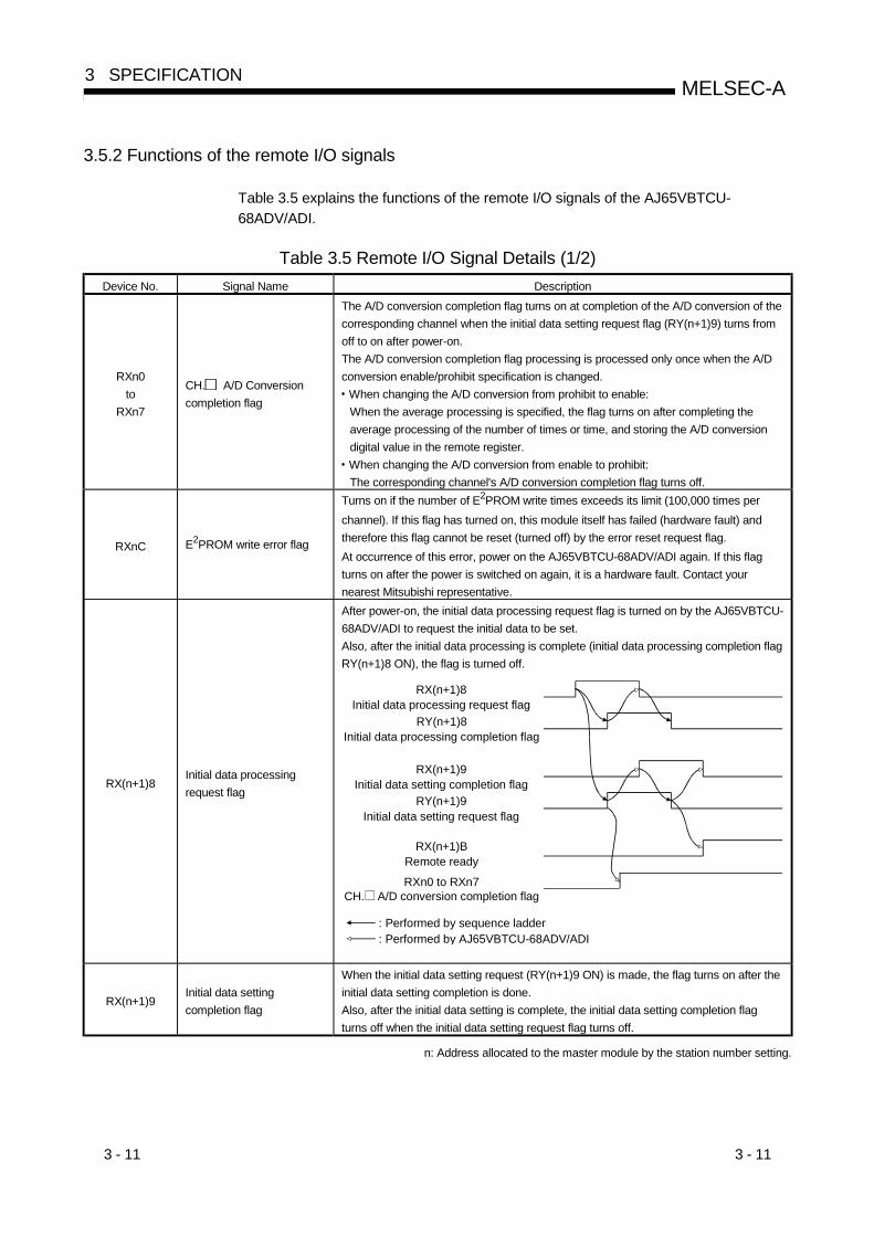
3.5.2 Functions of the remote I/O signals
Table 3.5 explains the functions of the remote I/O signals of the AJ65VBTCU-68ADV/ADI.
Table 3.5 Remote I/O Signal Details (1/2)Device No. Signal Name Description
RXn0to
RXn7
CH. A/D Conversioncompletion flag
The A/D conversion completion flag turns on at completion of the A/D conversion of thecorresponding channel when the initial data setting request flag (RY(n+1)9) turns fromoff to on after power-on.The A/D conversion completion flag processing is processed only once when the A/Dconversion enable/prohibit specification is changed. When changing the A/D conversion from prohibit to enable:When the average processing is specified, the flag turns on after completing theaverage processing of the number of times or time, and storing the A/D conversiondigital value in the remote register.
When changing the A/D conversion from enable to prohibit:The corresponding channel's A/D conversion completion flag turns off.
RXnC E2PROM write error flag
Turns on if the number of E2PROM write times exceeds its limit (100,000 times perchannel). If this flag has turned on, this module itself has failed (hardware fault) andtherefore this flag cannot be reset (turned off) by the error reset request flag.At occurrence of this error, power on the AJ65VBTCU-68ADV/ADI again. If this flagturns on after the power is switched on again, it is a hardware fault. Contact yournearest Mitsubishi representative.
RX(n+1)8Initial data processingrequest flag
After power-on, the initial data processing request flag is turned on by the AJ65VBTCU-68ADV/ADI to request the initial data to be set.Also, after the initial data processing is complete (initial data processing completion flagRY(n+1)8 ON), the flag is turned off.
RX(n+1)8Initial data processing request flag
RY(n+1)8Initial data processing completion flag
RX(n+1)9Initial data setting completion flag
RY(n+1)9Initial data setting request flag
RX(n+1)BRemote ready
: Performed by sequence ladder: Performed by AJ65VBTCU-68ADV/ADI
RXn0 to RXn7CH. A/D conversion completion flag
RX(n+1)9Initial data settingcompletion flag
When the initial data setting request (RY(n+1)9 ON) is made, the flag turns on after theinitial data setting completion is done.Also, after the initial data setting is complete, the initial data setting completion flagturns off when the initial data setting request flag turns off.
n: Address allocated to the master module by the station number setting.

3 - 12 3 - 12
MELSEC-A3 SPECIFICATION
Table 3.5 Remote I/O Signal Details (2/2)Device No. Signal Name Description
RX(n+1)A Error status flag
Turns on at occurrence of an input range setting error, average time/number of timessetting error or E2PROM write error (RXnC).Does not turn on at occurrence of the watchdog timer error. ("RUN" LED goes off.)
RY(n+1)AError reset request flag
RX(n+1)AError status flag
: Performed by sequence ladder: Performed by AJ65VBTCU-68ADV/ADI
RWrn+8Error code
Error code0 0
RX(n+1)B Remote READYTurns on when initial data setting is completed after power-on or at termination of thetest mode.(Used for interlocking read/write from/to the master module.)
RY(n+1)8Initial data processingcompletion flag
Turns on after initial data processing completion when initial data processing isrequested after power-on or test mode operation.
RY(n+1)9Initial data setting requestflag
Turns on at the time of initial data setting or changing.
RY(n+1)A Error reset request flagWhen this flag turns on, the error status flag (RX(n+1)A) is reset, but the E2PROMwrite error flag (RXnC) cannot be rest and therefore the error status flag remains on.
n: Address allocated to the master module by the station number setting.

3 - 13 3 - 13
MELSEC-A3 SPECIFICATION
3.6 Remote Register
The AJ65VBTCU-68ADV/ADI has a remote resister for data communication with themaster module. The remote register allocation and data structures are described.
3.6.1 Remote register allocation
The remote register allocation is shown in Table 3.6.
Table 3.6 Remote register allocationCommunication direction Address Description Default value Reference section
RWwm A/D conversion enable/prohibit specification 0 Section 3.6.2RWwm+1 CH.1 to 4 input range setting 0RWwm+2 CH.5 to 8 input range setting 0
Section 3.6.3
RWwm+3 Average processing specification 0 Section 3.6.4RWwm+4 CH.1 average time, number of times setting 0RWwm+5 CH.2 average time, number of times setting 0RWwm+6 CH.3 average time, number of times setting 0RWwm+7 CH.4 average time, number of times setting 0RWwm+8 CH.5 average time, number of times setting 0RWwm+9 CH.6 average time, number of times setting 0RWwm+A CH.7 average time, number of times setting 0
Master Remote
RWwm+B CH.8 average time, number of times setting 0
Section 3.6.5
RWrn CH.1 digital output value 0RWrn+1 CH.2 digital output value 0RWrn+2 CH.3 digital output value 0RWrn+3 CH.4 digital output value 0RWrn+4 CH.5 digital output value 0RWrn+5 CH.6 digital output value 0RWrn+6 CH.7 digital output value 0RWrn+7 CH.8 digital output value 0
Section 3.6.6
RWrn+8 Error code 0 Section 3.6.7
Remote Master
RWrn+9to
RWrn+BReserved 0 ——
m, n: Address allocated to the master module by the station number setting.
POINTDo not read or write data from or to the reserved area of the remote register. If datais read or written, we cannot guarantee the functions of the AJ65VBTCU-68ADV/ADI.

3 - 14 3 - 14
MELSEC-A3 SPECIFICATION
3.6.2 A/D conversion enable/prohibit specification (Address RWwm)
(1) Set whether A/D conversion is enabled or disabled per channel.
(2) By setting the unused channels to conversion prohibit, the sampling cycle can beshortened.
Example) The sampling cycle when only channels 1 and 3 are set to A/Dconversion enabled:
2 (Number of channels enabled) × 1ms (Conversion speed at one channel) = 2ms
(3) Operation is performed according to the setting made for the leading edges ofinitial data setting request flag (RY(n+1)9).
(4) The default setting is A/D conversion disable for all channels.b15 b14 b13 b12 b11 b10 b9 b8 b7 b6 b5 b4 b3 b2 b1
CH.2 CH.1
b0
Ignored
CH.3CH.4
1: Enable A/D conversion0: Prohibit A/D conversion
CH.6 CH.5CH.7CH.8
(5) AJ65VBTCU-68ADV/ADI processing when conversion isenabled/prohibited(a) Average processing initialization
The data in the work area stored by the AJ65VBTCU-68ADV/ADI system toperform the average processing is initialized.For example, at a channel with the average processing specification at 50times, if the conversion enable/prohibit is set after having completedsampling for 30 times, the 30 sampling data is all cleared, and then theaverage processing is performed from the initial state.
(b) A/D conversion completion flag processingThe A/D conversion completion flag processing is performed only oncewhen the A/D conversion enable/prohibit setting is changed. • When changed the A/D conversion from prohibit to enabled:
When the average processing is specified, the flag turns on afterperforming the average processing for the number of time or time andstoring the A/D conversion digital value in the remote register.
• When changed the A/D conversion from enabled to prohibited:The A/D conversion completion flag for the corresponding channel isturned off.

3 - 15 3 - 15
MELSEC-A3 SPECIFICATION
3.6.3 CH. input range setting (Address RWwm+1, RWwm+2)
(1) Set the analog input range per channel.
(2) Operation is performed according to the setting made for the leading edges of theinitial data setting request flag (RY(n+1)9).
(3) The default is as follows.AJ65VBTCU-68ADV: -10 to +10VAJ65VBTCU-68ADI : 4 to 20mA
b15 b12 b11 b8 b7 b4 b3 b0to
CH.4
to
CH.3
to
CH.2
to
CH.1RWwm+1
b15 b12 b11 b8 b7 b4 b3 b0to
CH.8
to
CH.7
to
CH.6
to
CH.5RWwm+2
Input Range Set Value-10 to +10V 0H
0 to 5V 1H
1 to 5V 2H
User range setting 1 (-10 to +10V) 3H
AJ65VBTCU-68ADV
User range setting 2 (0 to 5V) 4H
4to 20mA 0H
0 to 20mA 1HAJ65VBTCU-68ADIUser range setting (0 to 20mA) 2H
POINTIf the set value is outside the setting range, error "20 " occurs, the "RUN" LEDflickers at intervals of 0.1s, and all channels do not make A/D conversion.
indicates the channel No. where the error occurred.
3 - 16 3 - 16
MELSEC-A3 SPECIFICATION
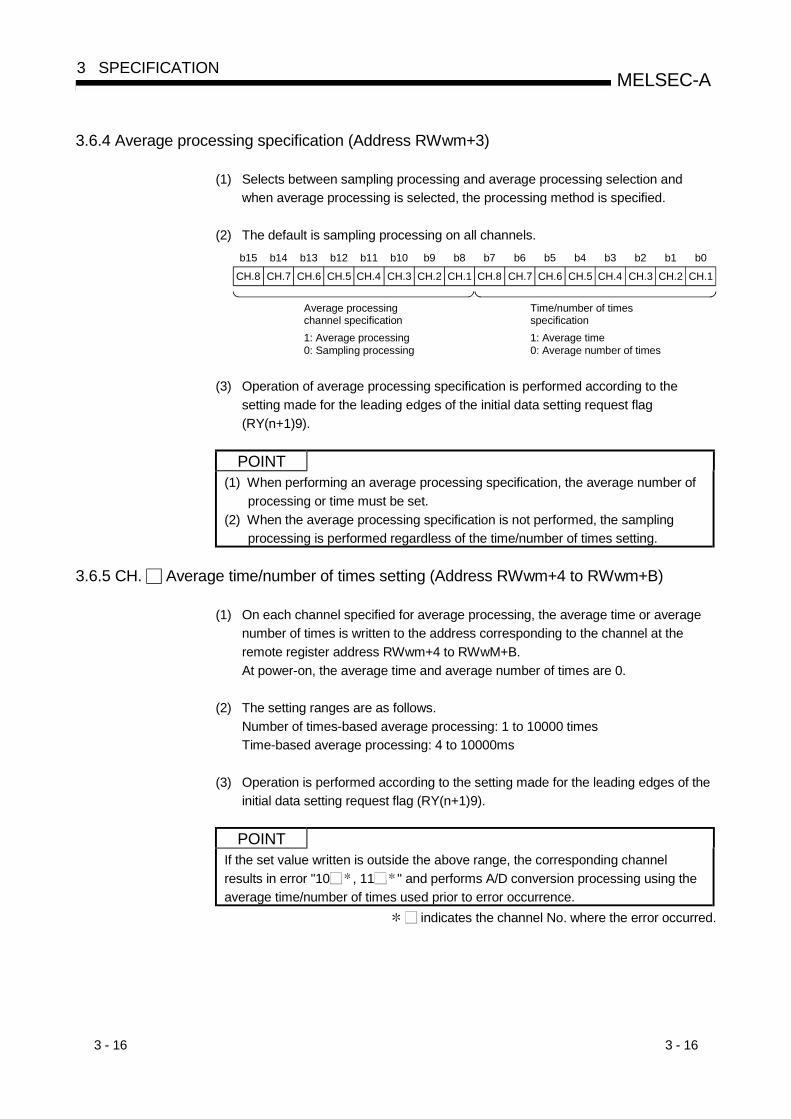
3.6.4 Average processing specification (Address RWwm+3)
(1) Selects between sampling processing and average processing selection andwhen average processing is selected, the processing method is specified.
(2) The default is sampling processing on all channels.b15 b14 b13 b12 b11 b10 b9 b8 b7 b6 b5 b4 b3 b2 b1
CH.2 CH.1
b0
CH.3CH.4CH.6 CH.5CH.7CH.8
Average processing channel specification 1: Average processing 0: Sampling processing
Time/number of times specification 1: Average time 0: Average number of times
CH.2 CH.1CH.3CH.4CH.6 CH.5CH.7CH.8
(3) Operation of average processing specification is performed according to thesetting made for the leading edges of the initial data setting request flag(RY(n+1)9).
POINT(1) When performing an average processing specification, the average number of
processing or time must be set.(2) When the average processing specification is not performed, the sampling
processing is performed regardless of the time/number of times setting.
3.6.5 CH. Average time/number of times setting (Address RWwm+4 to RWwm+B)
(1) On each channel specified for average processing, the average time or averagenumber of times is written to the address corresponding to the channel at theremote register address RWwm+4 to RWwM+B.At power-on, the average time and average number of times are 0.
(2) The setting ranges are as follows.Number of times-based average processing: 1 to 10000 timesTime-based average processing: 4 to 10000ms
(3) Operation is performed according to the setting made for the leading edges of theinitial data setting request flag (RY(n+1)9).
POINTIf the set value written is outside the above range, the corresponding channelresults in error "10 , 11 " and performs A/D conversion processing using theaverage time/number of times used prior to error occurrence.
indicates the channel No. where the error occurred.
3 - 17 3 - 17
MELSEC-A3 SPECIFICATION
3.6.6 CH. Digital output value (Address RWrn to RWrn+7)
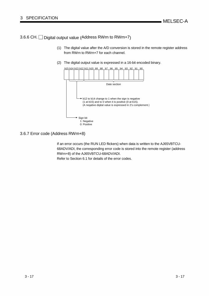
(1) The digital value after the A/D conversion is stored in the remote register addressfrom RWrn to RWrn+7 for each channel.
(2) The digital output value is expressed in a 16-bit encoded binary.b15 b14 b13 b12 b11 b10 b9 b8 b7 b6 b5 b4 b3 b2 b1 b0
Date section
b12 to b14 change to 1 when the sign is negative (1 at b15) and to 0 when it is positive (0 at b15).(A negative digital value is expressed in 2's complement.)
Sign bit 1: Negative 0: Positive
3.6.7 Error code (Address RWrn+8)
If an error occurs (the RUN LED flickers) when data is written to the AJ65VBTCU-68ADV/ADI, the corresponding error code is stored into the remote register (addressRWrn+8) of the AJ65VBTCU-68ADV/ADI.Refer to Section 6.1 for details of the error codes.
4 - 1 4 - 1
MELSEC-A4 SETUP AND PREPARATION BEFORE OPERATION
4 SETUP AND PREPARATION BEFORE OPERATION
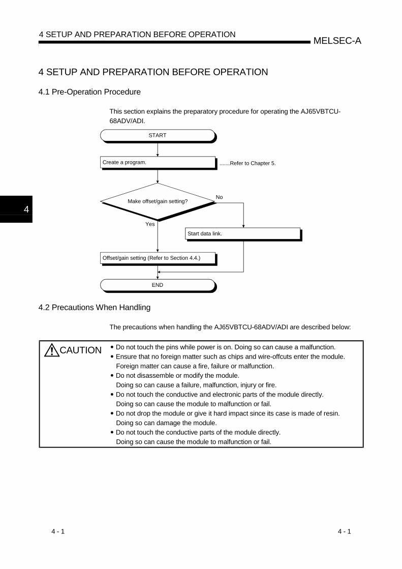
4.1 Pre-Operation Procedure
This section explains the preparatory procedure for operating the AJ65VBTCU-68ADV/ADI.
START
Start data link.
Make offset/gain setting?
Offset/gain setting (Refer to Section 4.4.)
END
.......Refer to Chapter 5.
No
Yes
Create a program.Create a program.
4.2 Precautions When Handling
The precautions when handling the AJ65VBTCU-68ADV/ADI are described below:
CAUTION Do not touch the pins while power is on. Doing so can cause a malfunction. Ensure that no foreign matter such as chips and wire-offcuts enter the module.Foreign matter can cause a fire, failure or malfunction.
Do not disassemble or modify the module.Doing so can cause a failure, malfunction, injury or fire.
Do not touch the conductive and electronic parts of the module directly.Doing so can cause the module to malfunction or fail.
Do not drop the module or give it hard impact since its case is made of resin.Doing so can damage the module.
Do not touch the conductive parts of the module directly.Doing so can cause the module to malfunction or fail.
4
4 - 2 4 - 2
MELSEC-A4 SETUP AND PREPARATION BEFORE OPERATION
CAUTION Dispose of the product as industrial waste. Use the module in the environment indicated in the general specifications given inthis manual.Not doing so can cause an electric shock, fire, malfunction, product damage ordeterioration.
Securely fix the module to a DIN rail or securely fix it with the CC-Link connectortype fitting.Not doing so can cause a drop or malfunction.
Mount or dismount the module to or from an enclosure after switching power offexternally in all phases. Not doing so can cause the module to fail or malfunction.
(1) When using the DIN rail adapter, install the DIN rail by making sure of thefollowing:(a) Applicable DIN rail models (conforming to the JIS C 2812)
TH35-7.5FeTH35-7.5Al
(b) DIN rail installation screw intervalWhen installing the DIN rail, tighten the screws with less than 200mm (7.87inch) pitches.
(2) As the CC-Link connector type metal installation fitting, use the narrow-width type(width 41)-dedicated fitting.(a) CC-Link connector type metal installation fitting model
A6PLT-J65V1
(3) Refer to the Master Module user's manual for specification, and manufacturers ofsupported cables for the use with AJ65VBTCU-68ADV/ADI.
4
4 - 3 4 - 3
MELSEC-A4 SETUP AND PREPARATION BEFORE OPERATION
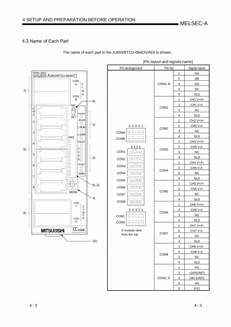
4.3 Name of Each Part
The name of each part in the AJ65VBTCU-68ADV/ADI is shown.
[Pin layout and signals name]Pin arrangement Pin No. Signal name
1 DA2 DB3 DG4 NC
CONA, B
5 SLD1 CH1 V+/I+2 CH1 V-/I-3 NC
CON1
4 SLD1 CH2 V+/I+2 CH2 V-/I-3 NC
CON2
4 SLD1 CH3 V+/I+2 CH3 V-/I-3 NC
CON3
4 SLD1 CH4 V+/I+2 CH4 V-/I-3 NC
CON4
4 SLD1 CH5 V+/I+2 CH5 V-/I-3 NC
CON5
4 SLD1 CH6 V+/I+2 CH6 V-/I-3 NC
CON6
4 SLD1 CH7 V+/I+2 CH7 V-/I-3 NC
CON7
4 SLD1 CH8 V+/I+2 CH8 V-/I-3 NC
CON8
4 SLD1 FG2 +24V(UNIT)3 24G (UNIT)4 AG
AJ65VBTCU-68ADCON
A
CONB
LINK
CH1
2
3
4
5
6
7
8
SEL
SET
SW1
POWER
RUN
L RUN
L ERR
TEST
1248
GAIN
OFFSET
MODE
POWER
CONC
COND
7)
3)
1)
9)
2)
5) ,6)
4)
10)
8)
CON2
CON1
CONA
CONB
CON3
CON4
CON5
CON6
CON7
CON8
1234
12345
CONC
COND
12345
A module viewfrom the top
CONC, D
5 FG1

4 - 4 4 - 4
MELSEC-A4 SETUP AND PREPARATION BEFORE OPERATION
NumberName and
appearanceDescription
POWERLED
ON : Power supply onOFF : Power supply off
Normalmode
On : Normal operationFlashing : 0.1s intervals: Input range setting error, mode select switch setting error
0.5s intervals: Average value setting (count) time errorOff : 24VDC power supply shutoff or watchdog timer error occurred
RUN LED
Testmode
On : Indicates that the SELECT/SET switch is in the SET position.Flashing : 0.5s intervals: An attempt was made to make setting outside the setting
range at the time of offset/gain setting.Off : Indicates that the SELECT/SET switch is in the SELECT or center position.
L RUNLED
On : Normal communicationOff : Communication cutoff (time expiration error)
1)Operation statusdisplay LED
L ERR.LED
On : Indicates that transmission speed setting or station number setting is outside the range.Flicker at fixed intervals : Indicates that transmission speed setting or station number setting
was changed from that at power-on.Flicker at unfixed intervals : Indicates that you forgot fitting the terminating resistor or the module
or CC-Link dedicated cable is affected by noise.Off : Indicates normal communications.Normalmode
Normally OFF
2)Offset/gainadjusting LEDs
TESTCHOFFSETGAIN
Testmode
TEST:ONThe OFFSET/GAIN/ CH LEDs lit change every time the SELECT/SET switch ismoved to SELECT. (Refer to section 4.4)
3)SELECT/SETswitch
Used to make offset/gain setting in the test mode.
Normal mode/ Test mode select switchAJ65VBTCU-68ADV AJ65VBTCU-68ADI
4)Mode selectswitch
0: Normal mode1: Test mode (user range setting 1)2: Test mode (user range setting 2)3 to 7: Must not be used
0: Normal mode1: Test mode (user range setting)2 to 7: Must not be used
Setting SwitchesSet Value
4 2 1Transmission Speed
0 OFF OFF OFF 156kbps1 OFF OFF ON 625kbps2 OFF ON OFF 2.5Mbps3 OFF ON ON 5.0Mbps4 ON OFF OFF 10Mbps
5)
Transmissionspeed settingswitches
1
2
4
B R
ATE
Always set the transmission speed within the above range.The switches are all factory-set to OFF.Making any other setting than the above will result in an error flickering the "L ERR." LED.Confirm the transmission speed setting switch numbers on the seal located on the side face of the connectorfor analog I/O.
4 - 5 4 - 5
MELSEC-A4 SETUP AND PREPARATION BEFORE OPERATION
NumberName and
appearanceDescription
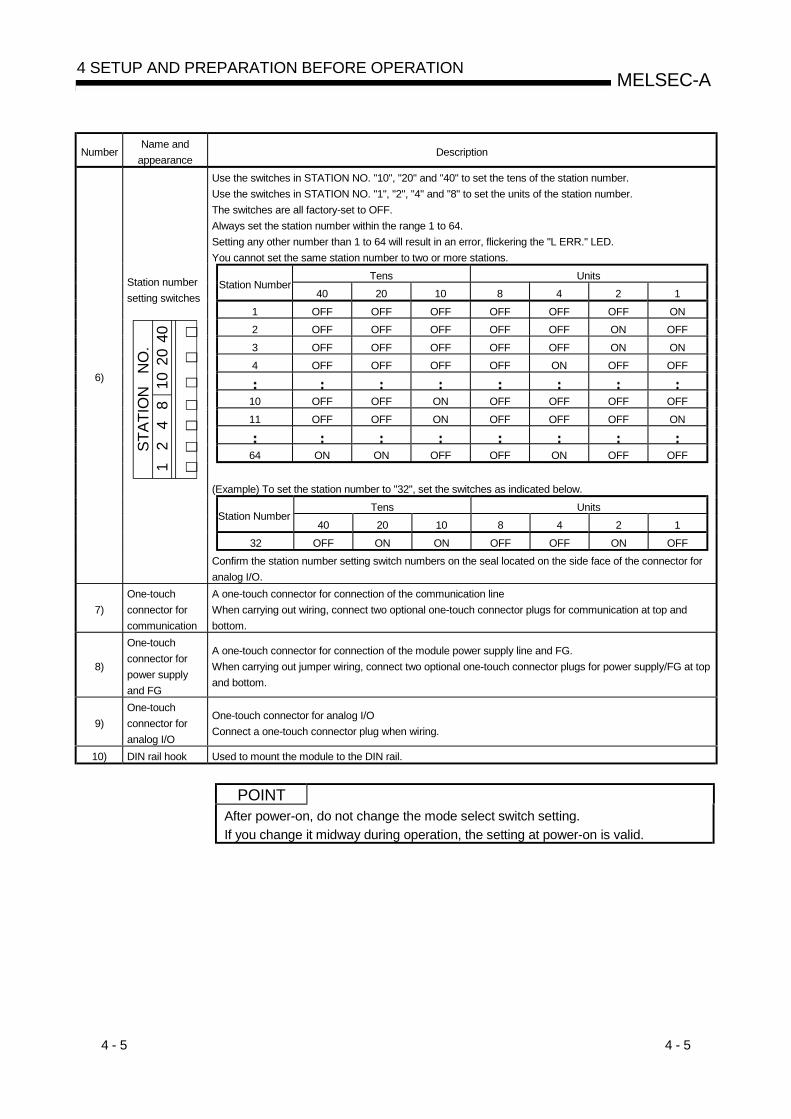
Use the switches in STATION NO. "10", "20" and "40" to set the tens of the station number.Use the switches in STATION NO. "1", "2", "4" and "8" to set the units of the station number.The switches are all factory-set to OFF.Always set the station number within the range 1 to 64.Setting any other number than 1 to 64 will result in an error, flickering the "L ERR." LED.You cannot set the same station number to two or more stations.
Tens UnitsStation Number
40 20 10 8 4 2 11 OFF OFF OFF OFF OFF OFF ON2 OFF OFF OFF OFF OFF ON OFF3 OFF OFF OFF OFF OFF ON ON4 OFF OFF OFF OFF ON OFF OFF
10 OFF OFF ON OFF OFF OFF OFF11 OFF OFF ON OFF OFF OFF ON
64 ON ON OFF OFF ON OFF OFF
(Example) To set the station number to "32", set the switches as indicated below.Tens Units
Station Number40 20 10 8 4 2 1
32 OFF ON ON OFF OFF ON OFF
6)
Station numbersetting switches
STAT
ION
N
O.
1 2
4
810
20
40
Confirm the station number setting switch numbers on the seal located on the side face of the connector foranalog I/O.
7)One-touchconnector forcommunication
A one-touch connector for connection of the communication lineWhen carrying out wiring, connect two optional one-touch connector plugs for communication at top andbottom.
8)
One-touchconnector forpower supplyand FG
A one-touch connector for connection of the module power supply line and FG.When carrying out jumper wiring, connect two optional one-touch connector plugs for power supply/FG at topand bottom.
9)One-touchconnector foranalog I/O
One-touch connector for analog I/OConnect a one-touch connector plug when wiring.
10) DIN rail hook Used to mount the module to the DIN rail.
POINTAfter power-on, do not change the mode select switch setting.If you change it midway during operation, the setting at power-on is valid.
4 - 6 4 - 6
MELSEC-A4 SETUP AND PREPARATION BEFORE OPERATION
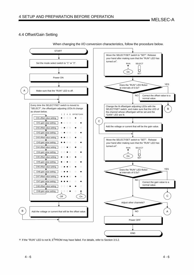
4.4 Offset/Gain Setting
When changing the I/O conversion characteristics, follow the procedure below.
Correct the gain value to a normal value.
ƒ‚ [ ƒh Ø Š· ƒX ƒC ƒb ƒ ‚ð g 1h org 2h ‚É Ý ’è ‚· ‚é B RUN SELECT
OnSET
START
Every time the SELECT/SET switch is moved to "SELECT", the offset/gain adjusting LEDs lit change as shown below.
1 2 4 8 OFFSETGAIN
A Make sure that the "RUN" LED is off.
Power ON
CH1 offset value setting
CH1 gain value setting
CH2 offset value setting
CH2 gain value setting
CH3 offset value setting
CH3 gain value setting
CH4 offset value setting
CH4 gain value setting
CH5 offset value setting
CH5 gain value setting
CH6 offset value setting
CH6 gain value setting
CH7 offset value setting
CH7 gain value setting
CH8 offset value setting
CH8 gain value setting
OnOff
ƒ‚ [ ƒh Ø Š· ƒX ƒC ƒb ƒ ‚ð g 1h org 2h ‚É Ý ’è ‚· ‚é BAdd the voltage or current that will be the offset value.B
YES
NO
B
RUN SELECT
OnSET
YES
NO
C
Adjust other channels?
NO A
Power OFF
END
Move the SELECT/SET switch to "SET". Release your hand after making sure that the "RUN" LED has turned on .
Change the lit offset/gain adjusting LEDs with the SELECT/SET switch, and make sure that the LED of the channel whose offset/gain will be set and the "GAIN" LED are lit.
Add the voltage or current that will be the gain value.
Move the SELECT/SET switch to "SET". Release your hand after making sure that the "RUN" LED has turned on .
Set the mode select switch to "1" or "2".
Does the "RUN" LED flicker at intervals of 0.5s?
Correct the offset value to a normal value.
Does the "RUN" LED flicker at intervals of 0.5s?
C
If the "RUN" LED is not lit, E2PROM may have failed. For details, refer to Section 3.5.2.
4 - 7 4 - 7
MELSEC-A4 SETUP AND PREPARATION BEFORE OPERATION
POINT(1) Set the offset and gain values in the actual usage state.(2) The offset and gain values are stored on E2PROM in the AJ65VBTCU-
68ADV/ADI and are not cleared at power-off.(3) Make offset/gain setting within the range indicated in POINT of Section 3.3.1
and Section 3.3.2. If setting is made outside this range, the maximumresolution/accuracy may not fall within the performance specifications range.
(4) When making offset/gain setting (in the test mode), choose the test mode(AJ65VBTCU-68ADV: 1, 2/AD65VBTCU-68ADI: 1) with the mode select switch.If the switch has been set to any unusable number, an error occurs and the"RUN" LED flickers at intervals of 0.1s.
(5) When the grounding indicated in Section 4.8.2 *5 is changed (not performed perform, or performed to removed), repeat the offset/gain setting from the start.
4 - 8 4 - 8
MELSEC-A4 SETUP AND PREPARATION BEFORE OPERATION
4.5 Station Number Setting
The station number setting of the AJ65VBTCU-68ADV/ADI determines the buffermemory addresses of the master module where the remote I/O signals and read/writedata are stored.For details, refer to the user's manual of the master module used.
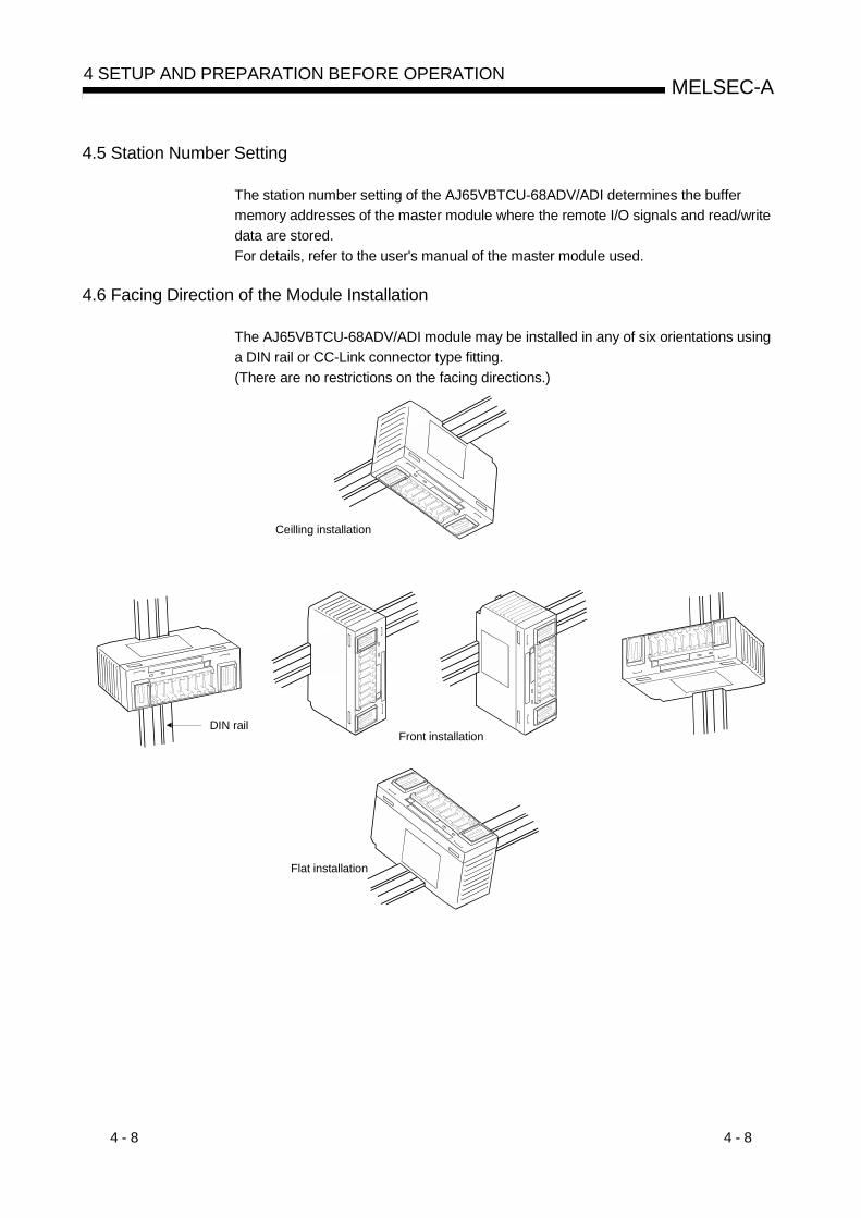
4.6 Facing Direction of the Module Installation
The AJ65VBTCU-68ADV/ADI module may be installed in any of six orientations usinga DIN rail or CC-Link connector type fitting.(There are no restrictions on the facing directions.)
DIN railFront installation
Flat installation
Ceilling installation
4 - 9 4 - 9
MELSEC-A4 SETUP AND PREPARATION BEFORE OPERATION
4.7 Data Link Cable Wiring
This section explains the wiring of the CC-Link dedicated cable used for connection ofthe AJ65VBTCU-68ADV/ADI and master module.
4.7.1 Instructions for handling the CC-Link dedicated cables
Do not handle the CC-Link dedicated cables roughly as described below. Doing so candamage the cables. Compact with a sharp object. Twist the cable excessively. Pull the cable hard. (more than the permitted elasticity.) Step on the cable. Place an object on the top. Scratch the cable's protective layer.
4 - 10 4 - 10
MELSEC-A4 SETUP AND PREPARATION BEFORE OPERATION
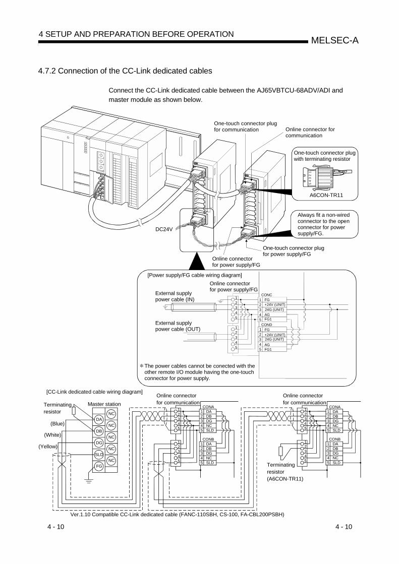
4.7.2 Connection of the CC-Link dedicated cables
Connect the CC-Link dedicated cable between the AJ65VBTCU-68ADV/ADI andmaster module as shown below.
The power cables cannot be conected with the other remote I/O module having the one-touch connector for power supply.
One-touch connector plug for power supply/FG
Online connector for communication
1 2 3 4 5
1 2 3 4 5
FG CONC
1 2 3 4 5
1 2 3 4 5
FG COND
+24V (UNIT)24G (UNIT)AGFG1
+24V (UNIT)24G (UNIT)AGFG1
DC24V
One-touch connector plugfor communication
Online connector for power supply/FG
Online connector for power supply/FG
[Power supply/FG cable wiring diagram]
External supplypower cable (IN)
External supply power cable (OUT)
One-touch connector plug with terminating resistor
54
32
1
54
32
1
A6CON-TR11
Always fit a non-wired connector to the open connector for power supply/FG.
Online connectorfor communication
DA
DB
DG
SLD
FG
NC
NC
NC
NC
NC
Master stationTerminatingresistor
Ver.1.10 Compatible CC-Link dedicated cable (FANC-110SBH, CS-100, FA-CBL200PSBH)
(Blue)
(White)
(Yellow)
[CC-Link dedicated cable wiring diagram]Online connectorfor communication
1 2 3 4 5
1 2 3 4 5
DA DB DG NC SLD
CONA
1 2 3 4 5
1 2 3 4 5
DA DB DG NC SLD
CONB
1 2 3 4 5
1 2 3 4 5
DA DB DG NC SLD
CONA
1 2 3 4 5
1 2 3 4 5
DA DB DG NC SLD
CONB
Terminatingresistor(A6CON-TR11)
4 - 11 4 - 11
MELSEC-A4 SETUP AND PREPARATION BEFORE OPERATION
POINT• On this unit, use the Ver. 1.10-compatible CC-Link dedicated cable (FANC-
110SBH, CS-110, FA-CBL200PSBH).You cannot use the Ver. 1.10-compatible CC-Link dedicated cables of other thanthe above types, CC-Link dedicated cables and CC-Link dedicated, high-performance cables.
• The shield cable of the CC-Link dedicated cable should be connected to "SLD" ineach module, and both ends should be grounded through "FG".SLD and FG are connected inside the module.
4.8 Wiring
This section provides the instructions for wiring the AJ65VBTCU-68ADV/ADI and itswiring with external equipment.
4.8.1 Wiring precautions
To obtain maximum performance from the functions of AJ65VBTCU-68ADV/ADI andimprove the system reliability, an external wiring with high durability against noise isrequired.The precautions when performing external wiring are as follows:(1) Use separate cables for the AC and AJ65VBTCU-68ADV/ADI external input
signals, in order not to be affected by the AC side surge or conductivity.
(2) Do not bundle or place with load carrying wires other than the main circuit line,high voltage line or PLC. Noises, surges, or conductivity may affect the system.
(3) Place a one-point grounding on the PLC side for the shielded line or shieldedcable. However, depending on the external noise conditions, it may be better havea grounding externally.
4 - 12 4 - 12
MELSEC-A4 SETUP AND PREPARATION BEFORE OPERATION
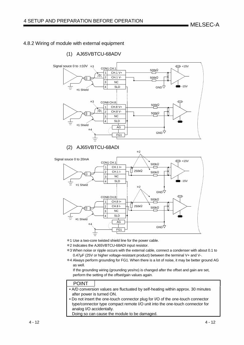
4.8.2 Wiring of module with external equipment
(1) AJ65VBTCU-68ADV
500k
CH.1 V+CH.1 V-
NCSLD
CH.8 V+CH.8 V-
NCSLD
FG1
CON1 CH.1+15V
-15V
CON8 CH.8
Signal souce 0 to 10V
AG
GND
1234
1234
GND
500k
500k
500k
3
3
41 Shield
1 Shield
(2) AJ65VBTCU-68ADI
FG1
+15V
-15V
Signal souce 0 to 20mA
AG
GND
CH.8 I+CH.8 I-
NCSLD
CON8 CH.81234
GND
CH.1 I+CH.1 I-
NCSLD
CON1 CH.11234
500k
500k250k
500k
500k250k
1 Shield
1 Shield
4
2
2
1 Use a two-core twisted shield line for the power cable.2 Indicates the AJ65VBTCU-68ADI input resistor.3 When noise or ripple occurs with the external cable, connect a condenser with about 0.1 to
0.47µF (25V or higher voltage-resistant product) between the terminal V+ and V-.4 Always perform grounding for FG1. When there is a lot of noise, it may be better ground AG
as well.If the grounding wiring (grounding yes/no) is changed after the offset and gain are set,perform the setting of the offset/gain values again.
POINT• A/D conversion values are fluctuated by self-heating within approx. 30 minutes
after power is turned ON.• Do not insert the one-touch connector plug for I/O of the one-touch connector
type/connector type compact remote I/O unit into the one-touch connector foranalog I/O accidentally.Doing so can cause the module to be damaged.
4 - 13 4 - 13
MELSEC-A4 SETUP AND PREPARATION BEFORE OPERATION
4.9 How to Wire the One-Touch Connector Plug
This section describes the way to wire the one-touch connector plug.Refer to section 2.3 for more information on the types and specifications of the one-touch connector plugs which conform to the AJ65VBTCU-68ADV/ADI.
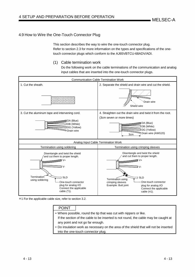
(1) Cable termination workDo the following work on the cable terminations of the communication and analoginput cables that are inserted into the one-touch connector plugs.
Communication Cable Termination Work
1. Cut the sheath. 2. Separate the shield and drain wire and cut the shield.
Shield wireDrain wire
3. Cut the aluminum tape and intervening cord.
DA (Blue)DB (White)DG (Yellow)Drain wire
4. Straighten out the drain wire and twist it from the root.(3cm seven or more times)
3cm
DA (Blue)DB (White)DG (Yellow)Drain wire (AWG20)
Analog Input Cable Termination WorkTermination using soldering Termination using crimping sleeves
V+
V-
Termination using soldering
One-touch connectorplug for analog I/OConnect the applicablecable (*1).
Disentangle and twist the shield and cut them to proper length.
SLD
V+
V-
Termination using crimping sleeves Example: Butt joint
One-touch connector plug for analog I/OConnect the applicablecable ( 1).
Disentangle and twist the shield and cut them to proper length.
SLD
1 For the applicable cable size, refer to section 3.2.
POINT• Where possible, round the tip that was cut with nippers or like.
If the section of the cable to be inserted is not round, the cable may be caught atany point and not go far enough.
• Do insulation work as necessary on the area of the shield that will not be insertedinto the one-touch connector plug.
4 - 14 4 - 14
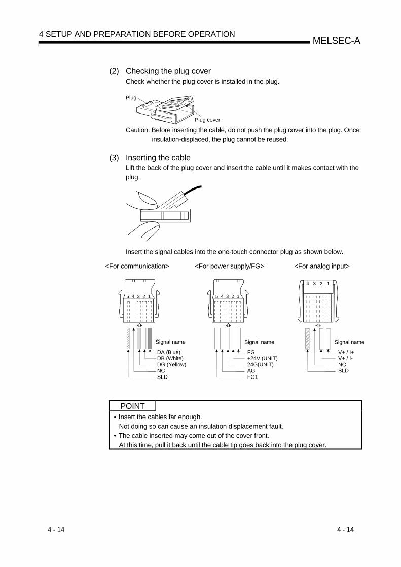
MELSEC-A4 SETUP AND PREPARATION BEFORE OPERATION
(2) Checking the plug coverCheck whether the plug cover is installed in the plug.
Plug
Plug cover
Caution: Before inserting the cable, do not push the plug cover into the plug. Onceinsulation-displaced, the plug cannot be reused.
(3) Inserting the cableLift the back of the plug cover and insert the cable until it makes contact with theplug.
Insert the signal cables into the one-touch connector plug as shown below.
<For communication> <For power supply/FG> <For analog input>
5 4 3 2 1
Signal name Signal name
4 3 2 1
DA (Blue) DB (White) DG (Yellow) NCSLD
FG +24V (UNIT) 24G(UNIT)AGFG1
V+ / I+ V+ / I- NCSLD
Signal name
5 4 3 2 1
POINT• Insert the cables far enough.
Not doing so can cause an insulation displacement fault.• The cable inserted may come out of the cover front.
At this time, pull it back until the cable tip goes back into the plug cover.
4 - 15 4 - 15
MELSEC-A4 SETUP AND PREPARATION BEFORE OPERATION
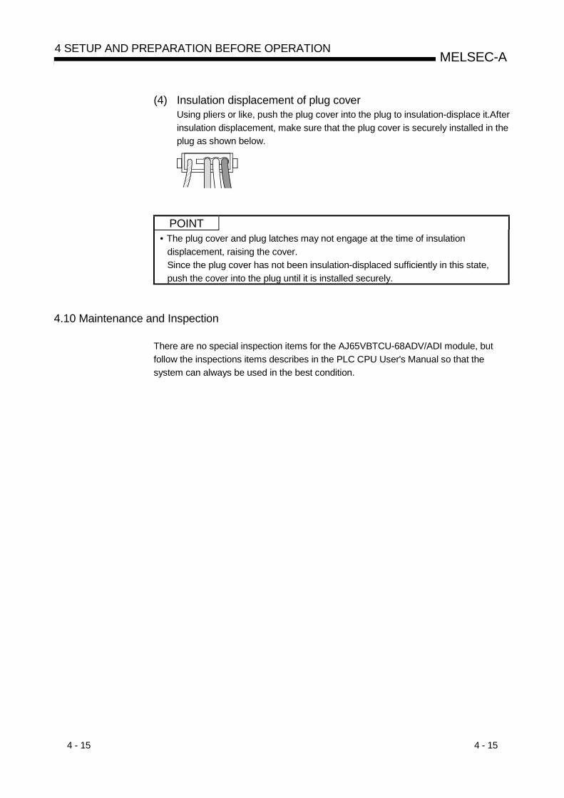
(4) Insulation displacement of plug coverUsing pliers or like, push the plug cover into the plug to insulation-displace it.Afterinsulation displacement, make sure that the plug cover is securely installed in theplug as shown below.
POINT• The plug cover and plug latches may not engage at the time of insulation
displacement, raising the cover.Since the plug cover has not been insulation-displaced sufficiently in this state,push the cover into the plug until it is installed securely.
4.10 Maintenance and Inspection
There are no special inspection items for the AJ65VBTCU-68ADV/ADI module, butfollow the inspections items describes in the PLC CPU User's Manual so that thesystem can always be used in the best condition.

5 - 1 5 - 1
MELSEC-A5 PROGRAMMING
5 PROGRAMMING
The programming procedure, basic read/write programs, and program examples forthe AJ765VBTCU-68ADV/ADI are described.When utilizing the program example introduced in this chapter for an actual system,fully verify that there are no problems in controllability in the target system.Refer to the user's manual of the master module used for the master module, toSection 3.6 for the remote registers, and to the AnSHCPU/AnACPU/AnUCPUProgramming Manual (Dedicated Instructions) for details of the dedicated instructions.
5.1 Programming Procedure
Create a program which executes the AJ765VBTCU-68ADV/ADI analog/digitalconversion by following the procedure below:
START
Perform average processing?
END
No
Yes
A/D conversion enable/prohibit specification
Input range setting
Average time, number of times setting
Specify the channel for which averageprocessing will be performed.
Read digital output value
Initial settings
When using the QCPU (Q mode), you can use the remote device stationinitialization procedure registration function to make settings. When using the ACPU,QCPU (A mode) or QnACPU, use the sequence program to make settings.
5
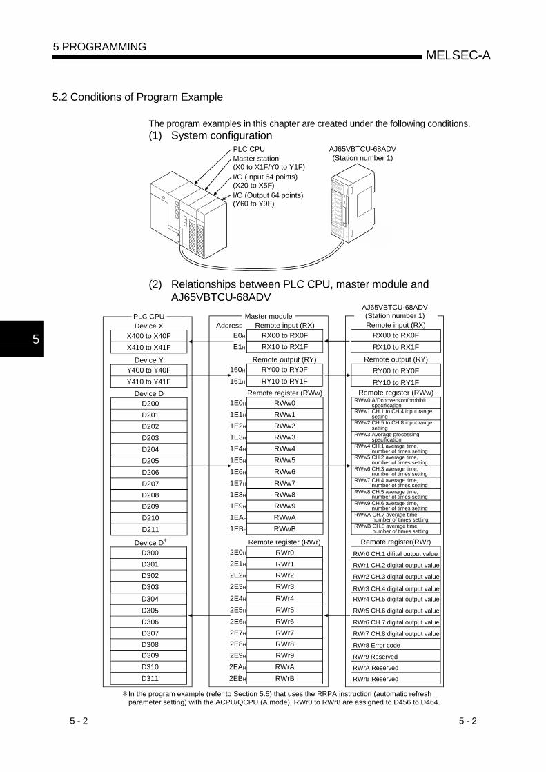
5 - 2 5 - 2
MELSEC-A5 PROGRAMMING
5.2 Conditions of Program Example
The program examples in this chapter are created under the following conditions.(1) System configuration
PLC CPUMaster station(X0 to X1F/Y0 to Y1F)
I/O (Output 64 points)(Y60 to Y9F)
AJ65VBTCU-68ADV(Station number 1)
I/O (Input 64 points)(X20 to X5F)
(2) Relationships between PLC CPU, master module andAJ65VBTCU-68ADV
AJ65VBTCU-68ADV(Station number 1)PLC CPU
Device XX400 to X40FX410 to X41F
Device YY400 to Y40FY410 to Y41F
Device DD200D201D202D203
Device DD300D301D302D303
Master moduleAddress Remote input (RX)
RX00 to RX0FRX10 to RX1F
E0H
E1H
Remote output (RY)RY00 to RY0FRY10 to RY1F
160H
161H
Remote register (RWw)RWw0RWw1RWw2RWw3
1E0H
1E1H
1E2H
1E3H
Remote register (RWr)RWr0RWr1RWr2RWr3
2E0H
2E1H
2E2H
2E3H
Remote input (RX)RX00 to RX0FRX10 to RX1F
Remote output (RY)RY00 to RY0FRY10 to RY1F
Remote register (RWw)
Remote register(RWr)
RWw0 A/Dconversion/prohibit
RWr0 CH.1 difital output value
D204D205D206D207
RWw4RWw5RWw6RWw7
1E4H
1E5H
1E6H
1E7H
RWw3 Average processing
D208D209D210D211
RWw8RWw9RWwARWwB
1E8H
1E9H
1EAH
1EBH
D304D305D306D307
RWr4RWr5RWr6RWr7
2E4H
2E5H
2E6H
2E7H
D308 RWr8RWr9RWrARWrB
2E8H
2E9H
2EAH
2EBH
RWr8 Error code
RWrA Reserved
RWrB Reserved
RWr9 Reserved
RWw1 CH.1 to CH.4 input range
RWw2 CH.5 to CH.8 input range
RWr1 CH.2 digital output value
RWr2 CH.3 digital output value
RWr3 CH.4 digital output valueRWr4 CH.5 digital output value
RWr5 CH.6 digital output value
RWr6 CH.7 digital output value
RWr7 CH.8 digital output value
D309D310D311
In the program example (refer to Section 5.5) that uses the RRPA instruction (automatic refreshparameter setting) with the ACPU/QCPU (A mode), RWr0 to RWr8 are assigned to D456 to D464.
RWw4 CH.1 average time, number of times settingRWw5 CH.2 average time, number of times settingRWw6 CH.3 average time, number of times settingRWw7 CH.4 average time, number of times settingRWw8 CH.5 average time, number of times settingRWw9 CH.6 average time, number of times settingRWwA CH.7 average time, number of times settingRWwB CH.8 average time, number of times setting
specification
setting
setting
spacification
5

5 - 3 5 - 3
MELSEC-A5 PROGRAMMING
POINTSome CPU modules may not accept the devices used in the program example inthis chapter. For the setting ranges of the devices, refer to the user's manual of theCPU module used.For the A1SCPU, for example, devices X100, Y100 and later are unusable. Usesuch devices as B and M.
(3) Initial settingsSetting Item Settings
A/D conversion enable/prohibitspecification (RWw0)
A/D conversion enabled channel: Channel 1, 2
CH. 1 to CH. 4 input range setting(RWw1)
Channel 1: 0 to 5VChannel 2: User range setting 1
Average processing specification(RWw3)
Channel 1: Sampling processingChannel 2: Average processing, number of times average
CH. 2 average time, number oftimes setting (RWw5)
Number of average processing times of channel 2: 16 times
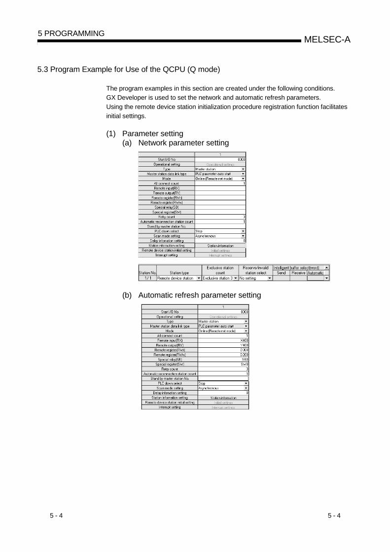
5 - 4 5 - 4
MELSEC-A5 PROGRAMMING
5.3 Program Example for Use of the QCPU (Q mode)
The program examples in this section are created under the following conditions.GX Developer is used to set the network and automatic refresh parameters.Using the remote device station initialization procedure registration function facilitatesinitial settings.
(1) Parameter setting(a) Network parameter setting
(b) Automatic refresh parameter setting
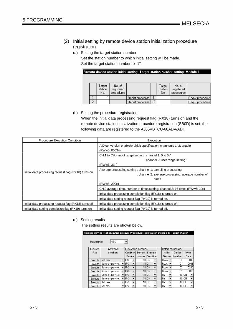
5 - 5 5 - 5
MELSEC-A5 PROGRAMMING
(2) Initial setting by remote device station initialization procedureregistration(a) Setting the target station number
Set the station number to which initial setting will be made.Set the target station number to "1".
(b) Setting the procedure registrationWhen the initial data processing request flag (RX18) turns on and theremote device station initialization procedure registration (SB0D) is set, thefollowing data are registered to the AJ65VBTCU-68ADV/ADI.
Procedure Execution Condition ExecutionA/D conversion enable/prohibit specification: channenls 1, 2: enable(RWw0 :0003H)CH.1 to CH.4 input range setting : channel 1: 0 to 5V
: channel 2: user range setting 1(RWw1: 31H)Average processing setting : channel 1: sampling processing
: channel 2: average processing, average number oftimes
(RWw3: 200H)CH.2 average time, number of times setting: channel 2: 16 times (RWw5: 10H)Initial data processing completion flag (RY18) is turned on.
Initial data processing request flag (RX18) turns on
Initial data setting request flag (RY19) is turned on.Initial data processing request flag (RX18) turns off Initial data processing completion flag (RY18) is turned off.Initial data setting completion flag (RX19) turns on Initial data setting request flag (RY19) is turned off.
(c) Setting resultsThe setting results are shown below.
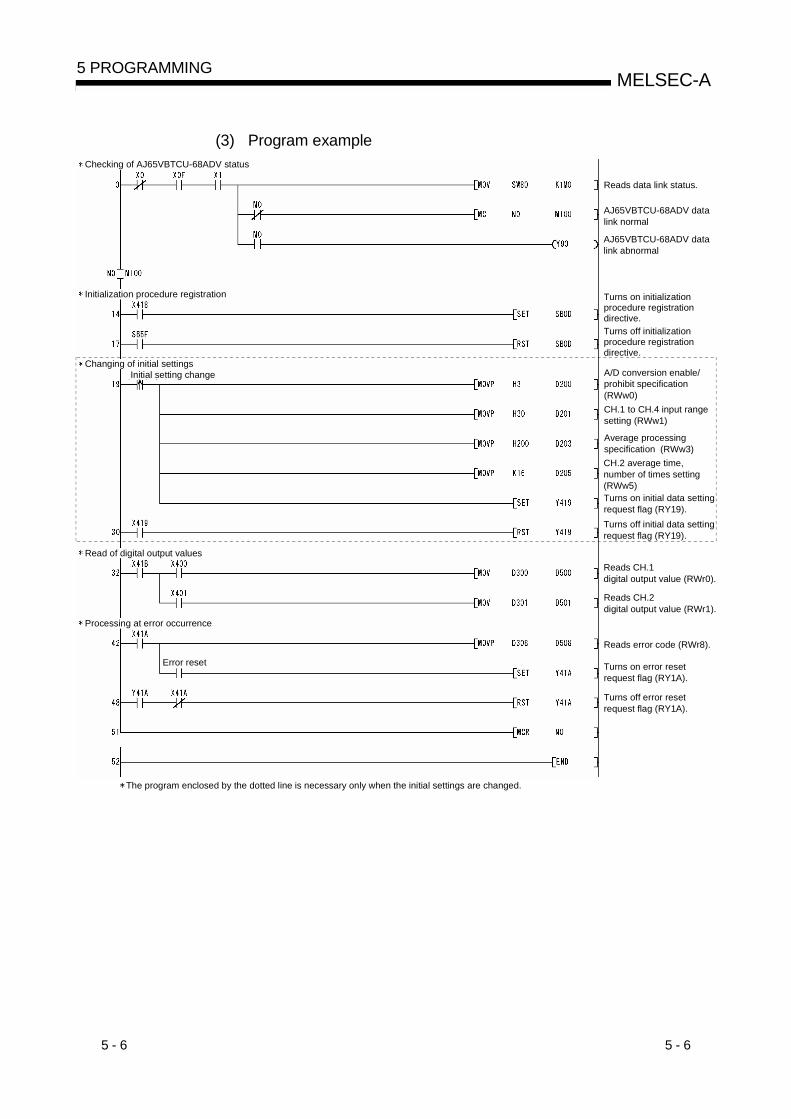
5 - 6 5 - 6
MELSEC-A5 PROGRAMMING
(3) Program example
Reads data link status.
AJ65VBTCU-68ADV data link normal
AJ65VBTCU-68ADV data link abnormal
A/D conversion enable/prohibit specification (RWw0)
Turns on initialization procedure registration directive.Turns off initialization procedure registration directive.
CH.1 to CH.4 input rangesetting (RWw1)
Average processingspecification (RWw3)CH.2 average time, number of times setting (RWw5)Turns on initial data settingrequest flag (RY19).Turns off initial data settingrequest flag (RY19).
Reads CH.1digital output value (RWr0).
Reads CH.2digital output value (RWr1).
Reads error code (RWr8).
Turns on error resetrequest flag (RY1A).
Turns off error resetrequest flag (RY1A).
ƒC ƒj ƒV ƒƒ ƒ‹Ý ’è •Ï X
Error reset
The program enclosed by the dotted line is necessary only when the initial settings are changed.
Checking of AJ65VBTCU-68ADV status
Initialization procedure registration
Changing of initial settingsInitial setting change
Read of digital output values
Processing at error occurrence
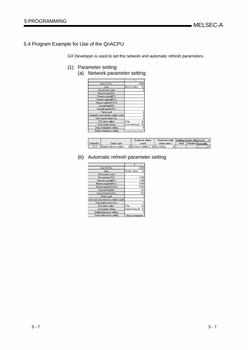
5 - 7 5 - 7
MELSEC-A5 PROGRAMMING
5.4 Program Example for Use of the QnACPU
GX Developer is used to set the network and automatic refresh parameters.
(1) Parameter setting(a) Network parameter setting
(b) Automatic refresh parameter setting
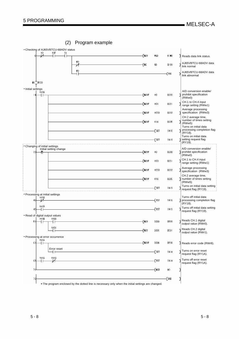
5 - 8 5 - 8
MELSEC-A5 PROGRAMMING
(2) Program example
Initial settings
Checking of AJ65VBTCU-68ADV status
Changing of initial settings Initial setting change
Processing at initial settings
Read of digital output values
Processing at error occurrence
Error reset
The program enclosed by the dotted line is necessary only when the initial settings are changed.
Reads data link status.
AJ65VBTCU-68ADV data link normal
AJ65VBTCU-68ADV data link abnormal
A/D conversion enable/prohibit specification(RWw0)CH.1 to CH.4 input range setting (RWw1)Average processingspecification (RWw3)CH.2 average time, number of times setting (RWw5)Turns on initial data processing completion flag(RY18).Turns on initial data setting request flag (RY19).
A/D conversion enable/prohibit specification (RWw0)CH.1 to CH.4 inputrange setting (RWw1)
Average processingspecification (RWw3)CH.2 average time, number of times setting (RWw5)Turns on initial data settingrequest flag (RY19).
Turns off initial data processing completion flag (RY18).Turns off initial data settingrequest flag (RY19).
Reads CH.1 digital output value (RWr0).
Reads CH.2 digital output value (RWr1).
Reads error code (RWr8).
Turns on error resetrequest flag (RY1A).
Turns off error resetrequest flag (RY1A).
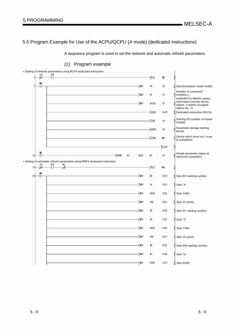
5 - 9 5 - 9
MELSEC-A5 PROGRAMMING
5.5 Program Example for Use of the ACPU/QCPU (A mode) (dedicated instructions)
A sequence program is used to set the network and automatic refresh parameters.
(1) Program exampleSetting of network parameters using RLPA dedicated instruction
Setting of automatic refresh parameters using RRPA dedicated instruction
Synchronization mode invalid
Number of connected modules:1AJ65VBTCU-68ADV station information (remote device station, 3 station occupied, station No. 1)Dedicated instruction (RLPA)
Starting I/O number of master module
Parameter storage starting device
Device which turns on 1 scanat completion
Reads parameter status at abnormal completion.
Sets RX starting number.
Sets "X".
Sets X400.
Sets RY starting number.
Sets 32 points.
Sets "Y".
Sets Y400.
Sets 32 points.
Sets RW starting number.
Sets "D".
Sets D200.
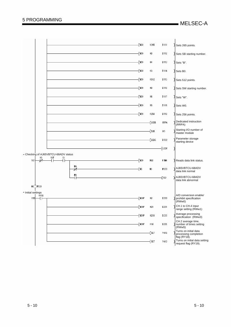
5 - 10 5 - 10
MELSEC-A5 PROGRAMMING
Checking of AJ65VBTCU-68ADV status
Initial settings
Sets 265 points.
Sets SB starting number.
Sets "B".
Sets B0.
Sets 512 points.
Sets SW starting number.
Sets "W".
Sets W0.
Sets 256 points.
Dedicated instruction (RRPA)
Starting I/O number ofmaster module
Parameter storagestarting device
Reads data link status.
AJ65VBTCU-68ADVdata link normal
AJ65VBTCU-68ADVdata link abnormal
A/D conversion enable/prohibit specification (RWw0)CH.1 to CH.4 input range setting (RWw1)
Average processingspecification (RWw3)CH.2 average time, number of times setting (RWw5)Turns on initial data processing completion flag (RY18).Turns on initial data setting request flag (RY19).

5 - 11 5 - 11
MELSEC-A5 PROGRAMMING
Initial setting changeChanging of initial settings
Processing at initial settings
Read of digital output values
Processing at error occurrence
Error reset
The program enclosed by the dotted line is necessary only when the initial settings are changed.
A/D conversion enable/prohibit specification(RWw0)CH.1 to CH.4 inputrange setting (RWw1)
Average processingspecification (RWw3)
CH.2 average time, numberof times setting (RWw5)
Turns on initial data settingrequest flag (RY19).
Turns off initial data processing completion flag (RY18).
Turns off initial data settingrequest flag (RY19).
Reads CH.1 digital output value (RWr0).
Reads CH.2 digital output value (RWr1).
Reads error code (RWr8).
Turns on error resetrequest flag (RY1A).
Turns off error resetrequest flag (RY1A).
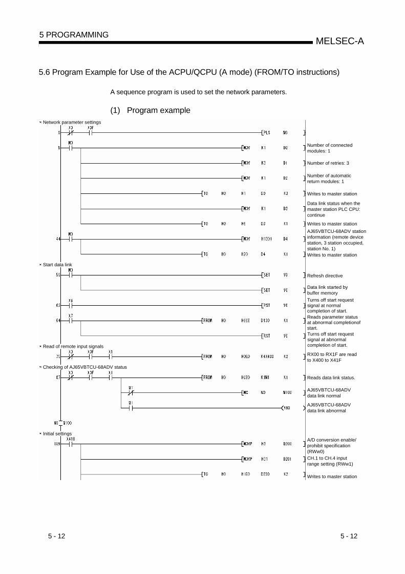
5 - 12 5 - 12
MELSEC-A5 PROGRAMMING
5.6 Program Example for Use of the ACPU/QCPU (A mode) (FROM/TO instructions)
A sequence program is used to set the network parameters.
(1) Program example
Number of connected modules: 1
Number of retries: 3
Number of automatic return modules: 1
Writes to master station
Data link status when themaster station PLC CPU: continue
AJ65VBTCU-68ADV station information (remote device station, 3 station occupied, station No. 1)Writes to master station
Writes to master station
Refresh directive
Data link started by buffer memoryTurns off start request signal at normal completion of start.Reads parameter status at abnormal completionof start.Turns off start request signal at abnormal completion of start.
AJ65VBTCU-68ADVdata link normal
AJ65VBTCU-68ADVdata link abnormal
RX00 to RX1F are read to X400 to X41F
Reads data link status.
A/D conversion enable/prohibit specification (RWw0)CH.1 to CH.4 input range setting (RWw1)
Writes to master station
Network parameter settings
Start data link
Read of remote input signals
Checking of AJ65VBTCU-68ADV status
Initial settings
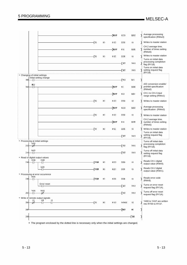
5 - 13 5 - 13
MELSEC-A5 PROGRAMMING
The program enclosed by the dotted line is necessary only when the initial settings are changed.
Initial setting change
Error reset
Average processing specification (RWw3)
Turns on initial data processing completion flag (RY18).Turns on initial data setting request flag (RY19).
A/D conversion enable/prohibit specification (RWw0)CH.1 to CH.4 input range setting (RWw1)
Writes to master station
Turns off initial data processing completion flag (RY18).
Turns off initial data setting request flag (RY19).
Reads CH.1 digital output value (RWr0).
Reads CH.2 digital output value (RWr1).
Turns on error reset request flag (RY1A).
Turns off error reset request flag (RY1A).
Y400 to Y41F are writteninto RY00 to RY1F.
Turns on initial data setting request flag (RY19).
Writes to master station
CH.2 average time, number of times setting (RWw5)Writes to master station
Average processing specification (RWw3)
Writes to master station
CH.2 average time, number of times setting (RWw5)
Writes to master station
Reads error code (RWr8).
Changing of initial settings
Processing at initial settings
Read of digital output values
Processing at error occurrence
Write of remote output signals
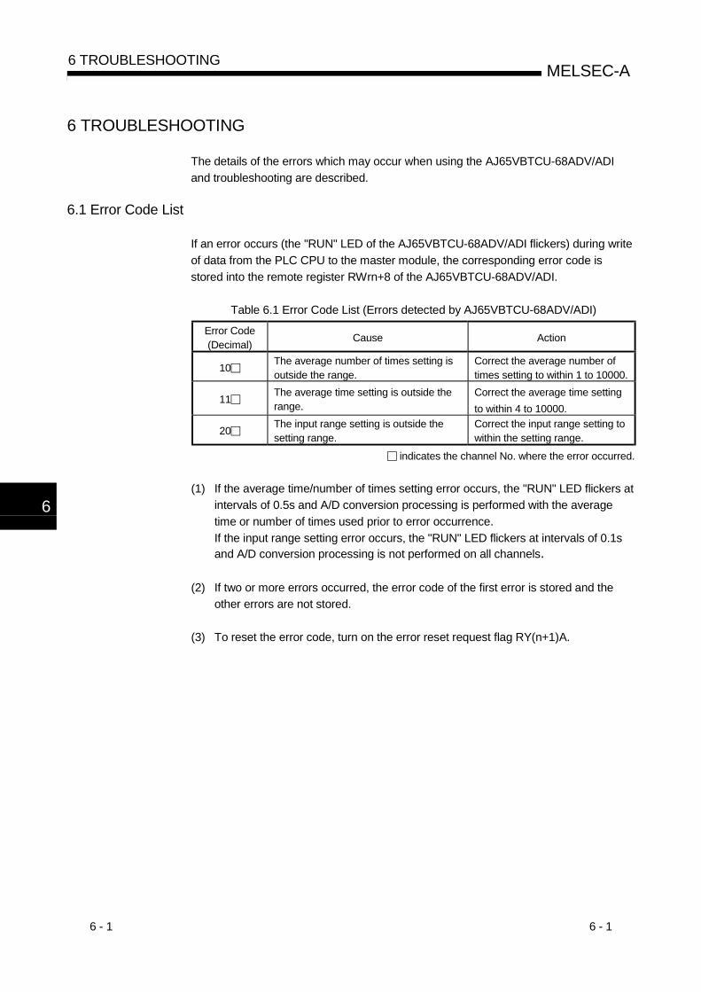
6 - 1 6 - 1
MELSEC-A6 TROUBLESHOOTING
6 TROUBLESHOOTING
The details of the errors which may occur when using the AJ65VBTCU-68ADV/ADIand troubleshooting are described.
6.1 Error Code List
If an error occurs (the "RUN" LED of the AJ65VBTCU-68ADV/ADI flickers) during writeof data from the PLC CPU to the master module, the corresponding error code isstored into the remote register RWrn+8 of the AJ65VBTCU-68ADV/ADI.
Table 6.1 Error Code List (Errors detected by AJ65VBTCU-68ADV/ADI)
Error Code(Decimal) Cause Action
10 The average number of times setting isoutside the range.
Correct the average number oftimes setting to within 1 to 10000.
11 The average time setting is outside therange.
Correct the average time settingto within 4 to 10000.
20 The input range setting is outside thesetting range.
Correct the input range setting towithin the setting range.
indicates the channel No. where the error occurred.
(1) If the average time/number of times setting error occurs, the "RUN" LED flickers atintervals of 0.5s and A/D conversion processing is performed with the averagetime or number of times used prior to error occurrence.If the input range setting error occurs, the "RUN" LED flickers at intervals of 0.1sand A/D conversion processing is not performed on all channels.
(2) If two or more errors occurred, the error code of the first error is stored and theother errors are not stored.
(3) To reset the error code, turn on the error reset request flag RY(n+1)A.
6
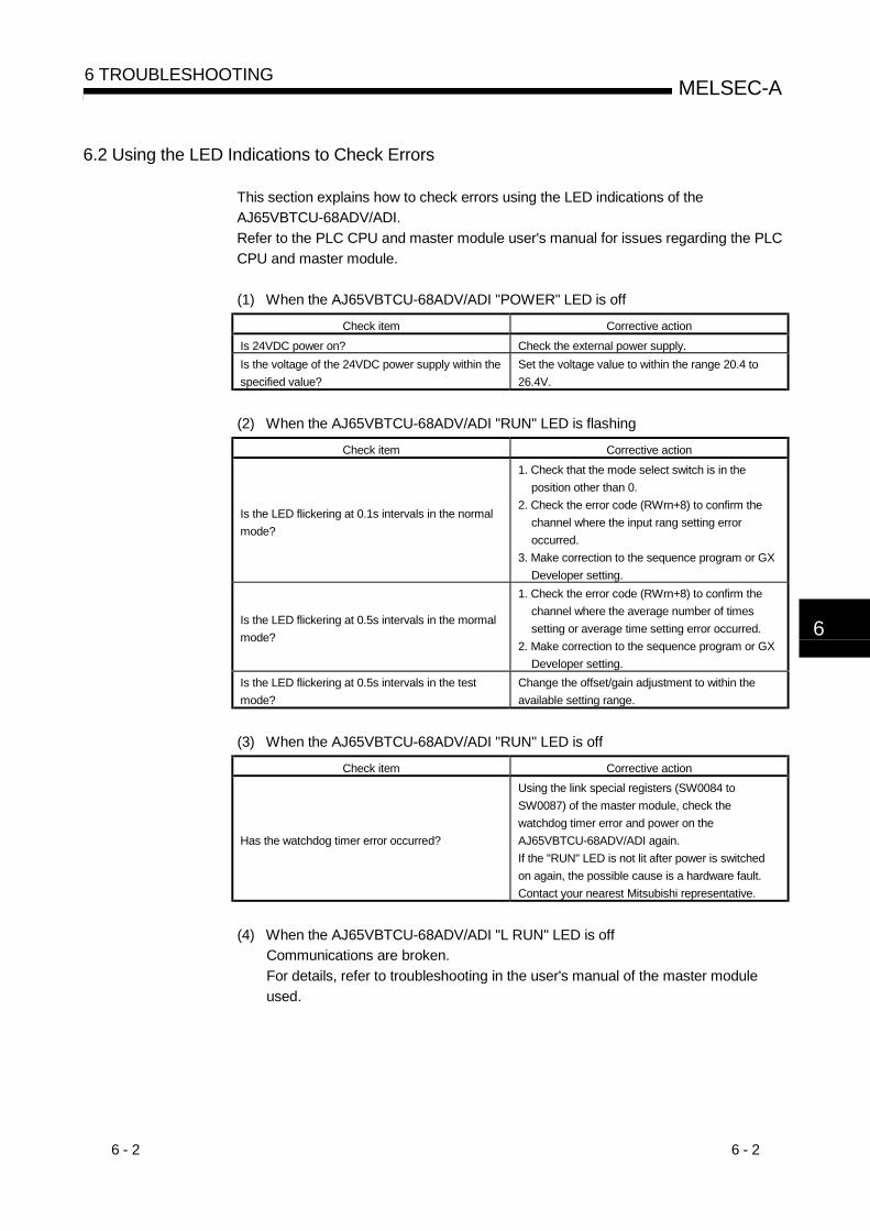
6 - 2 6 - 2
MELSEC-A6 TROUBLESHOOTING
6.2 Using the LED Indications to Check Errors
This section explains how to check errors using the LED indications of theAJ65VBTCU-68ADV/ADI.Refer to the PLC CPU and master module user's manual for issues regarding the PLCCPU and master module.
(1) When the AJ65VBTCU-68ADV/ADI "POWER" LED is off
Check item Corrective actionIs 24VDC power on? Check the external power supply.Is the voltage of the 24VDC power supply within thespecified value?
Set the voltage value to within the range 20.4 to26.4V.
(2) When the AJ65VBTCU-68ADV/ADI "RUN" LED is flashing
Check item Corrective action
Is the LED flickering at 0.1s intervals in the normalmode?
1. Check that the mode select switch is in theposition other than 0.
2. Check the error code (RWrn+8) to confirm thechannel where the input rang setting erroroccurred.
3. Make correction to the sequence program or GXDeveloper setting.
Is the LED flickering at 0.5s intervals in the mormalmode?
1. Check the error code (RWrn+8) to confirm thechannel where the average number of timessetting or average time setting error occurred.
2. Make correction to the sequence program or GXDeveloper setting.
Is the LED flickering at 0.5s intervals in the testmode?
Change the offset/gain adjustment to within theavailable setting range.
(3) When the AJ65VBTCU-68ADV/ADI "RUN" LED is off
Check item Corrective action
Has the watchdog timer error occurred?
Using the link special registers (SW0084 toSW0087) of the master module, check thewatchdog timer error and power on theAJ65VBTCU-68ADV/ADI again.If the "RUN" LED is not lit after power is switchedon again, the possible cause is a hardware fault.Contact your nearest Mitsubishi representative.
(4) When the AJ65VBTCU-68ADV/ADI "L RUN" LED is offCommunications are broken.For details, refer to troubleshooting in the user's manual of the master moduleused.
6
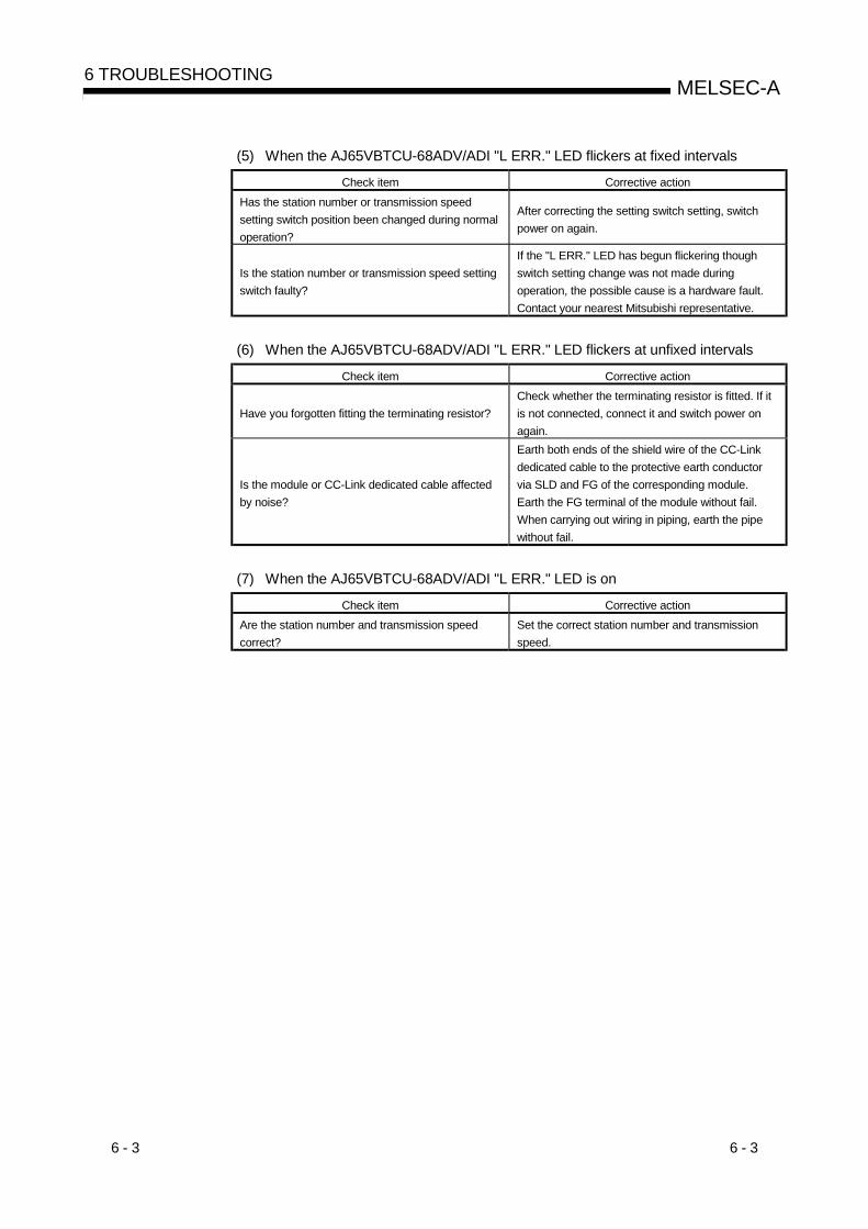
6 - 3 6 - 3
MELSEC-A6 TROUBLESHOOTING
(5) When the AJ65VBTCU-68ADV/ADI "L ERR." LED flickers at fixed intervals
Check item Corrective actionHas the station number or transmission speedsetting switch position been changed during normaloperation?
After correcting the setting switch setting, switchpower on again.
Is the station number or transmission speed settingswitch faulty?
If the "L ERR." LED has begun flickering thoughswitch setting change was not made duringoperation, the possible cause is a hardware fault.Contact your nearest Mitsubishi representative.
(6) When the AJ65VBTCU-68ADV/ADI "L ERR." LED flickers at unfixed intervals
Check item Corrective action
Have you forgotten fitting the terminating resistor?Check whether the terminating resistor is fitted. If itis not connected, connect it and switch power onagain.
Is the module or CC-Link dedicated cable affectedby noise?
Earth both ends of the shield wire of the CC-Linkdedicated cable to the protective earth conductorvia SLD and FG of the corresponding module.Earth the FG terminal of the module without fail.When carrying out wiring in piping, earth the pipewithout fail.
(7) When the AJ65VBTCU-68ADV/ADI "L ERR." LED is on
Check item Corrective actionAre the station number and transmission speedcorrect?
Set the correct station number and transmissionspeed.

6 - 4 6 - 4
MELSEC-A6 TROUBLESHOOTING
6.3 When the digital output value cannot be read
Check item Corrective actionIs the "POWER" LED off? Take action as described in Section 6.2 (1).Is the "RUN" LED flashing or off? Take action as described in Section 6.2 (2), (3).Is the "L RUN" LED off? Take action as described in Section 6.2 (4).
Is the "L ERR." LED on?Take action as described in Section 6.2 (7).Check the error details according to the mastermodule user's manual.
Is the PLC CPU "RUN" LED flashing or off?Check the error details according to the PLC CPUuser's manual.
Is the master module "RUN" LED off?Check the error details according to the mastermodule user's manual.
Is the master module [RD] [SD] LED on?Check the error details according to the mastermodule user's manual.
Is the analog input signal line disconnected, cut off,or any errors?
Check the error area by checking the signal linevisually or by conductive check.
Remove the AJ65VBTCU-68ADV/ADI analog inputcable. Apply the test voltage (stable power supplyor battery) to this module's terminal, and measurethe digital output value.
If he AJ65VBTCU-68ADV/ADI module digital outputvalue is normal, the effects are being received bynoise from an external wiring. So check the wiringand grounding method.Lift the AJ65VBTCU-68ADV/ADI from the system,and remove the grounding circuit. (install to the DINrail.)
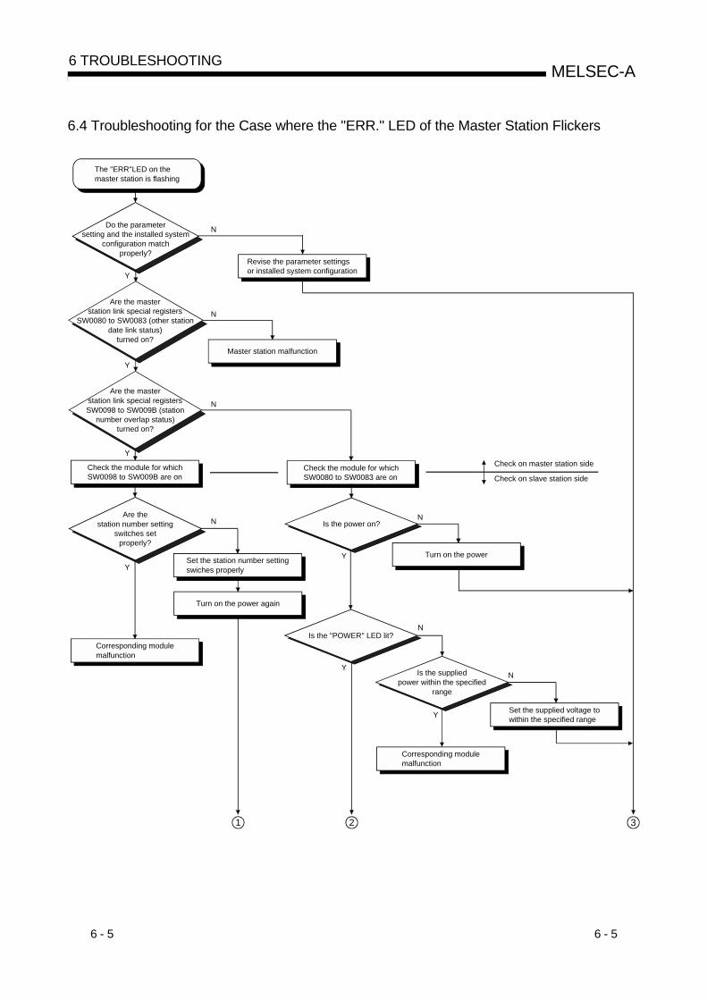
6 - 5 6 - 5
MELSEC-A6 TROUBLESHOOTING
6.4 Troubleshooting for the Case where the "ERR." LED of the Master Station Flickers
The "ERR"LED on the master station is flashing
Do the parametersetting and the installed system
configuration matchproperly?
Are the masterstation link special registers
SW0080 to SW0083 (other stationdate link status)
turned on?
Are the masterstation link special registersSW0098 to SW009B (station
number overlap status)turned on?
Check the module for whichSW0098 to SW009B are on
Are the station number setting
switches set properly?
Set the station number settingswiches properly
Revise the parameter settingsor installed system configuration
Master station malfunction
Check the module for whichSW0080 to SW0083 are on
Is the power on?
Turn on the power
Corresponding modulemalfunction
Turn on the power again
Is the "POWER" LED lit?
Is the suppliedpower within the specified
range
Set the supplied voltage towithin the specified range
Corresponding modulemalfunction
1 2 3
Check on master station side
Check on slave station side
N
N
N
N
Y
Y
Y
N
N
Y
Y
YY
N
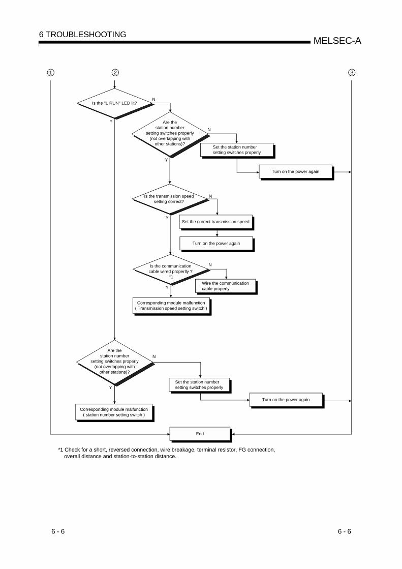
6 - 6 6 - 6
MELSEC-A6 TROUBLESHOOTING
Are thestation number
setting switches properly(not overlapping with
other stations)?Set the station numbersetting switches properly
Set the correct transmission speed
Is the transmission speed setting correct?
Corresponding module malfunction( Transmission speed setting switch )
Is the communicationcable wired properlly ?
*1
1 2 3
N
N
N
Y
Is the "L RUN" LED lit?N
Turn on the power again
Turn on the power again
Wire the communicationcable properly
Are thestation number
setting switches properly(not overlapping with
other stations)?
Set the station number setting switches properly
Corresponding module malfunction( station number setting switch )
End
Turn on the power again
Y
Y
Y
Y
N
*1 Check for a short, reversed connection, wire breakage, terminal resistor, FG connection, overall distance and station-to-station distance.
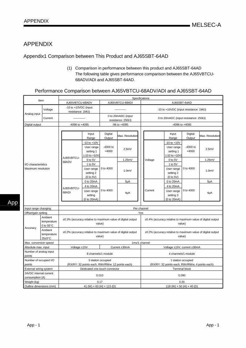
App - 1 App - 1
MELSEC-AAPPENDIX
APPENDIX
Appendix1 Comparison between This Product and AJ65SBT-64AD
(1) Comparison in performance between this product and AJ65SBT-64ADThe following table gives performance comparison between the AJ65VBTCU-68ADV/ADI and AJ65SBT-64AD.
Performance Comparison between AJ65VBTCU-68ADV/ADI and AJ65SBT-64ADSpecifications
ItemAJ65VBTCU-68ADV AJ65VBTCU-68ADI AJ65SBT-64AD
Voltage-10 to +10VDC (input
resistance: 1M )———— -10 to +10VDC (input resistance: 1M )
Analog inputCurrent ————
0 to 20mADC (inputresistance: 250 )
0 to 20mADC (input resistance: 250 )
Digital output -4096 to +4095 -96 to +4095 -4096 to +4095
InputRange
DigitalOutput
Max. ResolutionInput
RangeDigitalOutput
Max. Resolution
-10 to +10V -10 to +10VUser range
setting 1(-10 to +10V)
-4000 to+4000
2.5mV User rangesetting 1
(-10 to +10V)
-4000 to+4000
2.5mV
0 to 5V 1.25mV 0 to 5V 1.25mV1 to 5V 1 to 5V
AJ65VBTCU-68ADV
User rangesetting 2(0 to 5V)
0 to 40001.0mV
Voltage
User rangesetting 2(0 to 5V)
0 to 40001.0mV
0 to 20mA 5µA 0 to 20mA 5µA4 to 20mA 4 to 20mA
AJ65VBTCU-68ADI User range
setting(0 to 20mA)
0 to 40004µA
Current User rangesetting 3
(0 to 20mA)
0 to 40004µA
I/O characteristicsMaximum resolution
Input range changing Per channelOffset/gain setting Yes
Ambienttemperature0 to 55°C
±0.3% (accuracy relative to maximum value of digital outputvalue)
±0.4% (accuracy relative to maximum value of digital outputvalue)
AccuracyAmbienttemperature25±5°C
±0.2% (accuracy relative to maximum value of digital outputvalue)
±0.2% (accuracy relative to maximum value of digital outputvalue)
Max. conversion speed 1ms/1 channelAbsolute max. input Voltage ±15V Current ±30mA Voltage ±15V, current ±30mANumber of analog inputpoints
8 channels/1 module 4 channels/1 module
Number of occupied I/Opoints
3 station occupied(RX/RY: 32 points each, RWr/RWw: 12 points each)
1 station occupied(RX/RY: 32 points each, RWr/RWw: 4 points each)
External wiring system Dedicated one-touch connector Terminal block24VDC internal currentconsumption (A)
0.010 0.090
Weight (kg) 0.17 0.20Outline dimensions (mm) 41 (W) × 63 (H) × 115 (D) 118 (W) × 50 (H) × 40 (D)
App

App - 2 App - 2
MELSEC-AAPPENDIX
(2) Differences between AJ65VBTCU-68ADV/ADI and AJ65SBT-64ADSince the remote I/O signals, remote registers and so on differ, replacementcannot be made.• The AJ65VBTCU-68ADV is a voltage input-dedicated model.• The AJ65VBTCU-68ADI is a current input-dedicated model.
App
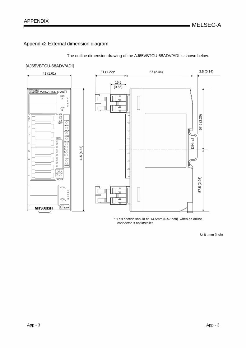
App - 3 App - 3
MELSEC-AAPPENDIX
Appendix2 External dimension diagram
The outline dimension drawing of the AJ65VBTCU-68ADV/ADI is shown below.
115
(4.5
3)
41 (1.61)
[AJ65VBTCU-68ADV/ADI]
AJ65VBTCU-68ADCON
A
CONB
LINK
CH1
2
3
4
5
6
7
8
SEL
SET
SW1
POWER
RUN
L RUN
L ERR
TEST
1248
GAIN
OFFSET
MODE
POWER
CONC
COND
67 (2.44)
DIN
rail
3.5 (0.14)
57.5
(2.2
6)57
.5 (2
.26)
31 (1.22)*
16.5(0.65)
* :This section should be 14.5mm (0.57inch) when an online connector is not installed.
Unit : mm (inch)

App - 4 App - 4
MELSEC-AAPPENDIX
MEMO
Index - 1 Index - 1
INDEX
[A]A/D conversion completion flag .................... 3-11A/D conversion enable/prohibit specification................................................. 3-14Absolute maximum input................................. 3-2Accuracy.................................................... 3-2,3-6Analog input..................................................... 3-2Analog input points.......................................... 3-2Applicable master modules............................. 2-2Average processing ........................................ 3-9Average processing specification ................. 3-16Average time, number of times setting......... 3-16
[C]CC-Link dedicated cable................................. 4-9CC-Link dedicated instruction......................... 2-2Comparison in performance between this product and AJ65SBT-64AD..............App-1Conversion speed ........................................... 3-7Current consumption....................................... 3-2Current input characteristics ........................... 3-5
[D]Data link cable wiring ...................................... 4-9Difference between AJ65VBTCU-68ADV/ADI and AJ65SBT-64AD..................................App-2Digital output.................................................... 3-2Digital output value........................................ 3-17DIN rail .................................................3-2,4-2,4-5
[E]E2PROM write error flag ............................... 3-11Error code........................................................ 6-1Error reset request flag ................................. 3-12Error status flag ............................................. 3-12External dimension diagram .......................App-3External power supply..................................... 3-2
[F]Facing direction of the module installation ..... 4-8Function list...................................................... 3-8
[G]Gain value........................................................ 3-3General specification....................................... 3-1
[I]I/O Conversion Characteristics........................3-3Initial data processing completion flag ..........3-12Initial data processing request flag................3-11Initial data setting completion flag .................3-11Initial data setting request flag.......................3-12Input range changing function .........................3-8Input range setting .........................................3-15
[M]Maintenance and inspection..........................4-15Maximum resolution.................................. 3-2,3-6Mode select switch...........................................4-4
[N]Name of each part ...........................................4-3Number of occupied stations...........................3-2
[O]Offset value ......................................................3-3Offset/gain adjusting LED................................4-4Offset/Gain Setting...........................................4-6One-touch connector for analog I/O................4-5One-touch connector for communication........4-5One-touch connector for power supply/FG.....4-5Operation status display LED..........................4-4
[P]Parts sold separately .......................................2-3Performance comparison between AJ65SBT-64AD and conventional product..................................................................... App-1Performance specification ...............................3-2Plug for one-touch connector ................. 2-3,4-10Pre-Operation procedure.................................4-1Precautions when handling .............................4-1Program example for use of the ACPU/ QCPU (A mode) (dedicated instructions) .....5-9Program example for use of the ACPU/ QCPU (A mode) (FROM/TO instructions) .5-12Program example for use of the QCPU (Q mode) ............................................5-4Program example for use of the QnACPU......5-7Programming procedure..................................5-1
Ind
Index - 2 Index - 2
[R]Remote I/O signal list .................................... 3-10Remote READY ............................................ 3-12Remote register allocation ............................ 3-13Resolution........................................................ 3-6
[S]Sampling processing....................................... 3-9SELECT/SET switch ....................................... 4-4Station number setting switch......................... 4-5
[T]Troubleshooting............................................... 6-1Troubleshooting for the case where the"ERR."LED of the master station flickers ....... 6-5
[U]User rage setting ....................................... 3-4,3-5
[V]Voltage input characteristics ........................... 3-4
[W]Weight.............................................................. 3-2Wiring............................................................. 4-11Wiring of module with external equipment ... 4-12
Ind

WARRANTY
Please confirm the following product warranty details before starting use.
1. Gratis Warranty Term and Gratis Warranty RangeIf any faults or defects (hereinafter "Failure") found to be the responsibility of Mitsubishi occurs during use of the productwithin the gratis warranty term, the product shall be repaired at no cost via the dealer or Mitsubishi Service Company.Note that if repairs are required at a site overseas, on a detached island or remote place, expenses to dispatch anengineer shall be charged for.[Gratis Warranty Term]
The gratis warranty term of the product shall be for one year after the date of purchase or delivery to a designatedplace.Note that after manufacture and shipment from Mitsubishi, the maximum distribution period shall be six (6) months, andthe longest gratis warranty term after manufacturing shall be eighteen (18) months. The gratis warranty term of repairparts shall not exceed the gratis warranty term before repairs.
[Gratis Warranty Range](1) The range shall be limited to normal use within the usage state, usage methods and usage environment, etc.,
which follow the conditions and precautions, etc., given in the instruction manual, user's manual and caution labelson the product.
(2) Even within the gratis warranty term, repairs shall be charged for in the following cases.1. Failure occurring from inappropriate storage or handling, carelessness or negligence by the user. Failure caused
by the user's hardware or software design.2. Failure caused by unapproved modifications, etc., to the product by the user.3. When the Mitsubishi product is assembled into a user's device, Failure that could have been avoided if functions
or structures, judged as necessary in the legal safety measures the user's device is subject to or as necessaryby industry standards, had been provided.
4. Failure that could have been avoided if consumable parts (battery, backlight, fuse, etc.) designated in theinstruction manual had been correctly serviced or replaced.
5. Failure caused by external irresistible forces such as fires or abnormal voltages, and Failure caused by forcemajeure such as earthquakes, lightning, wind and water damage.
6. Failure caused by reasons unpredictable by scientific technology standards at time of shipment from Mitsubishi.7. Any other failure found not to be the responsibility of Mitsubishi or the user.
2. Onerous repair term after discontinuation of production(1) Mitsubishi shall accept onerous product repairs for seven (7) years after production of the product is discontinued.
Discontinuation of production shall be notified with Mitsubishi Technical Bulletins, etc.(2) Product supply (including repair parts) is not possible after production is discontinued.
3. Overseas serviceOverseas, repairs shall be accepted by Mitsubishi's local overseas FA Center. Note that the repair conditions at each FACenter may differ.
4. Exclusion of chance loss and secondary loss from warranty liabilityRegardless of the gratis warranty term, Mitsubishi shall not be liable for compensation to damages caused by any causefound not to be the responsibility of Mitsubishi, chance losses, lost profits incurred to the user by Failures of Mitsubishiproducts, damages and secondary damages caused from special reasons regardless of Mitsubishi's expectations,compensation for accidents, and compensation for damages to products other than Mitsubishi products and other duties.
5. Changes in product specificationsThe specifications given in the catalogs, manuals or technical documents are subject to change without prior notice.
6. Product application(1) In using the Mitsubishi MELSEC programmable logic controller, the usage conditions shall be that the application will
not lead to a major accident even if any problem or fault should occur in the programmable logic controller device, andthat backup and fail-safe functions are systematically provided outside of the device for any problem or fault.
(2) The Mitsubishi general-purpose programmable logic controller has been designed and manufactured for applicationsin general industries, etc. Thus, applications in which the public could be affected such as in nuclear power plants andother power plants operated by respective power companies, and applications in which a special quality assurancesystem is required, such as for Railway companies or National Defense purposes shall be excluded from theprogrammable logic controller applications.Note that even with these applications, if the user approves that the application is to be limited and a special quality isnot required, application shall be possible.When considering use in aircraft, medical applications, railways, incineration and fuel devices, manned transportdevices, equipment for recreation and amusement, and safety devices, in which human life or assets could be greatlyaffected and for which a particularly high reliability is required in terms of safety and control system, please consultwith Mitsubishi and discuss the required specifications.
Mitsubishi Programmable Controller
Analog-Digital Converter Module type AJ65VBTCU-68ADV/ADI
User,s Manual
Specifications subject to change without notice.
MODEL
MODELCODE
AJ65V-68AD-U-SY-E
13JR41
SH(NA)-080181-B(0110)MEE
Analog-Digital Converter Module type AJ65VBTCU-68ADV/ADI
User,s Manual
U
When exported from Japan, this manual does not require application to theMinistry of Economy, Trade and Industry for service transaction permission.
HEAD OFFICE : 1-8-12, OFFICE TOWER Z 14F HARUMI CHUO-KU 104-6212,JAPANNAGOYA WORKS : 1-14 , YADA-MINAMI 5 , HIGASHI-KU, NAGOYA , JAPAN
![Safety Relay Module User's Manual - MITSUBISHI ELECTRIC …dl.mitsubishielectric.com/dl/fa/document/manual/plc/sh... · 2016-12-19 · A - 3 [Installation Precautions] [Wiring Precautions]](https://img.pdfslide.us/doc/110x75/5e8a074a03ac1b2a630583ae/safety-relay-module-users-manual-mitsubishi-electric-dl-2016-12-19-a-3-installation.jpg)


![FX3U-232ADP Installation Manual - MITSUBISHI …dl.mitsubishielectric.com/dl/fa/document/manual/plc_fx/...[11] Screws to fix the cable connector: Screw holes #4-40UNC (inch screw thread)](https://img.pdfslide.us/doc/110x75/5aafd4157f8b9a3a038de56b/fx3u-232adp-installation-manual-mitsubishi-dl-11-screws-to-fix-the-cable.jpg)