Embed Size (px)
Citation preview
S-8229 Series
www.ablicinc.com BATTERY MONITORING IC
© ABLIC Inc., 2012-2017 Rev.1.1_01
1
The S-8229 Series is a battery monitoring IC developed using CMOS technology. Compared with conventional CMOS voltage detectors, the S-8229 Series is ideal for the applications that require high-withstand voltage due to its maximum operation voltage as high as 24 V. The S-8229 Series is capable of confirming the voltage in stages since it detects three voltage values.
Features
Detection voltage accuracy: 1.0% Hysteresis characteristics: VHYS1 to VHYS3 = 0 mV, 50 mV, 300 mV, 400 mV, 500 mV Current consumption: During operation: IDD1 = 9.0 A max. (VDETtotal
*1 42 V) IDD1 = 11.0 A max. (VDETtotal
*1 42 V) During power-off: IDD2 = 0.1 A max. Operation voltage range: VDD = 3.6 V to 24 V Detection voltage: VDET1(S) to VDET3(S) = 10.5 V to 21.5 V (0.1 V step) Output form: Nch open-drain output Output logic*2: Full charge all on, full charge all off Operation temperature range: Ta = 40C to 85C Lead-free (Sn 100%), halogen-free *1. VDETtotal: Total detection voltage VDETtotal = VDET1(S) VDET2(S) VDET3(S) *2. Full charge all on: When the input voltage is equal to or higher than each of the three detection voltage values, VOUT1 = VOUT2 = VOUT3 = VSS. Full charge all off: When the input voltage is equal to or higher than each of the three detection voltage values, VOUT1 = VOUT2 = VOUT3 = "High-Z".
Application
Rechargeable lithium-ion battery pack
Packages
SOT-23-6 SNT-6A
www.ablic.com
BATTERY MONITORING IC S-8229 Series Rev.1.1_01
2
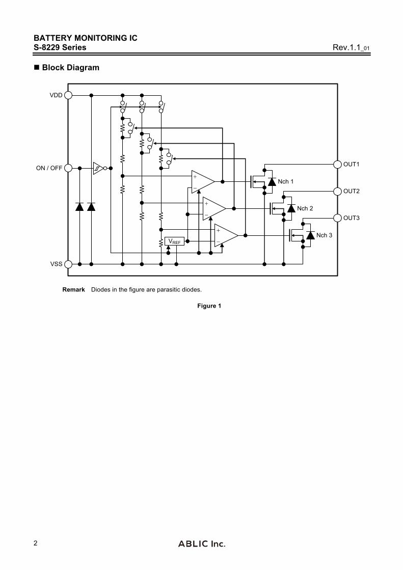
Block Diagram
OUT3
Nch 3
VDD
VREF
OUT2
Nch 2
OUT1
Nch 1
ON / OFF
VSS
Remark Diodes in the figure are parasitic diodes.
Figure 1
BATTERY MONITORING IC Rev.1.1_01 S-8229 Series
3
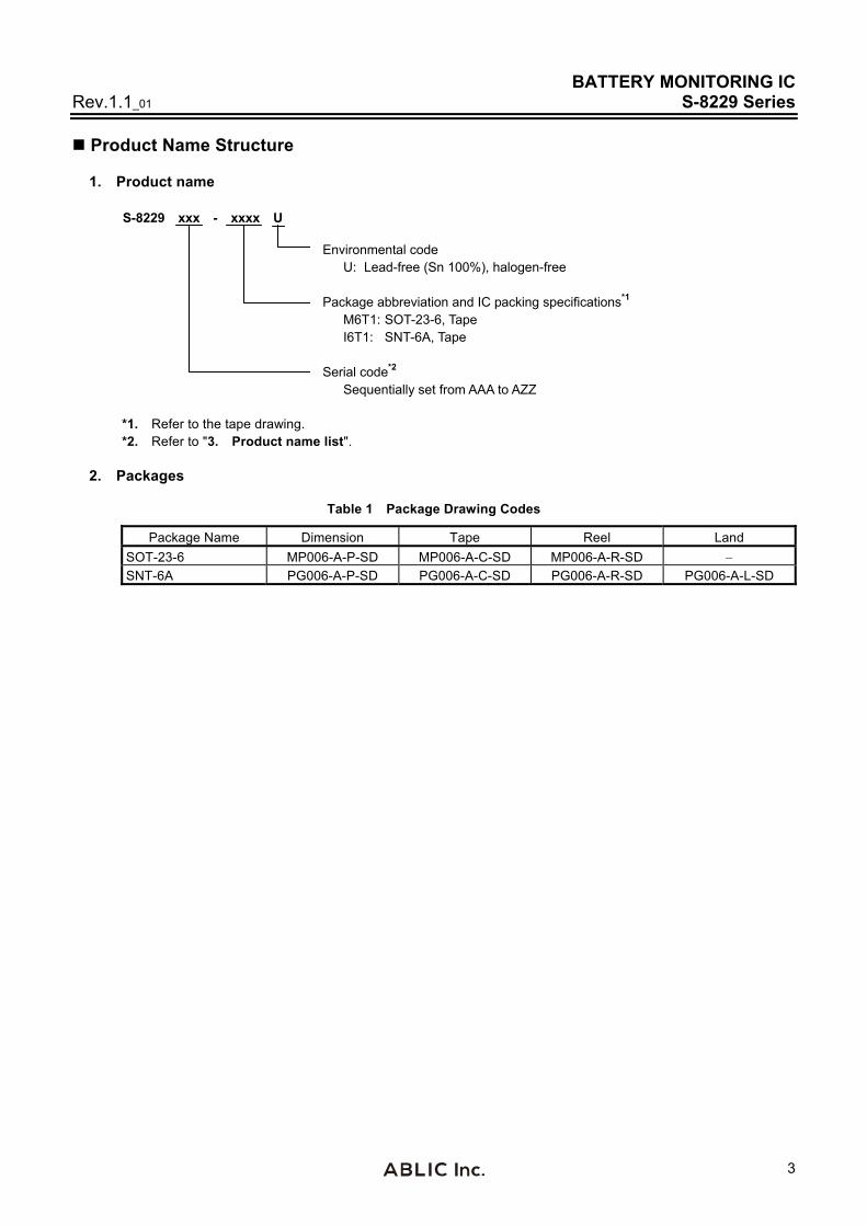
Product Name Structure
1. Product name
S-8229 xxx - xxxx U
Environmental code U: Lead-free (Sn 100%), halogen-free Package abbreviation and IC packing specifications*1 M6T1: SOT-23-6, Tape I6T1: SNT-6A, Tape Serial code*2 Sequentially set from AAA to AZZ
*1. Refer to the tape drawing. *2. Refer to "3. Product name list".
2. Packages
Table 1 Package Drawing Codes
Package Name Dimension Tape Reel Land
SOT-23-6 MP006-A-P-SD MP006-A-C-SD MP006-A-R-SD SNT-6A PG006-A-P-SD PG006-A-C-SD PG006-A-R-SD PG006-A-L-SD

BATTERY MONITORING IC S-8229 Series Rev.1.1_01
4
3. Product name list
3. 1 SOT-23-6
Table 2
Product Name Detection Voltage 1 [VDET1(S)]
Detection Voltage 2[VDET2(S)]
Detection Voltage 3[VDET3(S)]
Hysteresis Width 1 [VHYS1(S)]
Hysteresis Width 2 [VHYS2(S)]
Hysteresis Width 3 [VHYS3(S)]
Output Logic*1
S-8229AAA-M6T1U 19.400 V 18.100 V 15.300 V 0 V 0 V 0 V Full charge all on
S-8229AAB-M6T1U 19.400 V 18.100 V 15.300 V 0.500 V 0.500 V 0.500 V Full charge all on
S-8229AAC-M6T1U 19.500 V 18.000 V 15.500 V 0.050 V 0.050 V 0.050 V Full charge all on
S-8229AAG-M6T1U 15.600 V 14.800 V 13.600 V 0.500 V 0.500 V 0.500 V Full charge all on
S-8229AAH-M6T1U 20.000 V 18.500 V 16.000 V 0.500 V 0.500 V 0.500 V Full charge all on
S-8229AAI-M6T1U 20.000 V 18.500 V 16.000 V 0.050 V 0.050 V 0.050 V Full charge all on
S-8229AAJ-M6T1U 15.100 V 14.300 V 13.100 V 0.500 V 0.500 V 0.500 V Full charge all on
S-8229AAK-M6T1U 15.600 V 14.400 V 12.400 V 0 V 0 V 0 V Full charge all on
*1. Full charge all on: When the input voltage is equal to or higher than each of the three detection voltage values, VOUT1 = VOUT2 = VOUT3 = VSS.
Full charge all off: When the input voltage is equal to or higher than each of the three detection voltage values, VOUT1 = VOUT2 = VOUT3 = "High-Z".
Remark Please contact our sales office for products other than the above. 3. 2 SNT-6A
Table 3
Product Name Detection Voltage 1 [VDET1(S)]
Detection Voltage 2[VDET2(S)]
Detection Voltage 3[VDET3(S)]
Hysteresis Width 1 [VHYS1(S)]
Hysteresis Width 2 [VHYS2(S)]
Hysteresis Width 3 [VHYS3(S)]
Output Logic*1
S-8229AAF-I6T1U 18.000 V 15.000 V 21.500 V 0.050 V 0.050 V 0.050 V Full charge all on
*1. Full charge all on: When the input voltage is equal to or higher than each of the three detection voltage values, VOUT1 = VOUT2 = VOUT3 = VSS.
Full charge all off: When the input voltage is equal to or higher than each of the three detection voltage values, VOUT1 = VOUT2 = VOUT3 = "High-Z".
Remark Please contact our sales office for products other than the above.
BATTERY MONITORING IC Rev.1.1_01 S-8229 Series
5
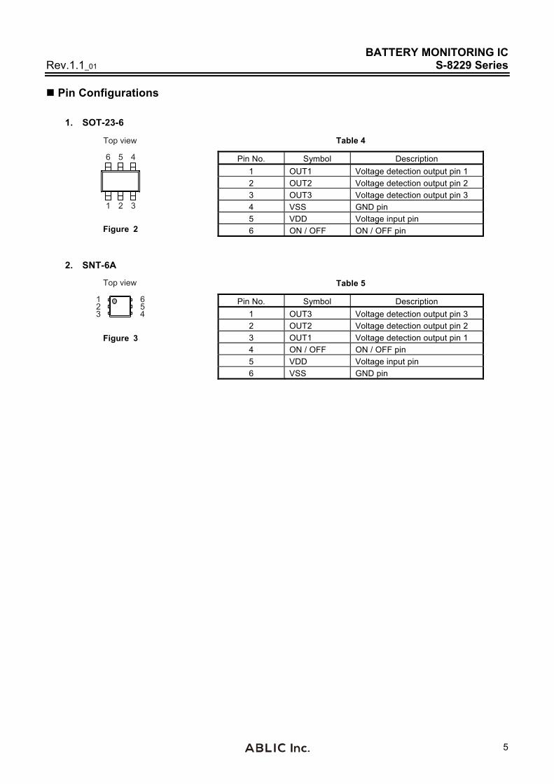
Pin Configurations
1. SOT-23-6
1 32
5 46
Top view
Figure 2
Table 4
Pin No. Symbol Description
1 OUT1 Voltage detection output pin 1
2 OUT2 Voltage detection output pin 2
3 OUT3 Voltage detection output pin 3
4 VSS GND pin
5 VDD Voltage input pin
6 ON / OFF ON / OFF pin
2. SNT-6A
54
623
1
Top view
Figure 3
Table 5
Pin No. Symbol Description
1 OUT3 Voltage detection output pin 3
2 OUT2 Voltage detection output pin 2
3 OUT1 Voltage detection output pin 1
4 ON / OFF ON / OFF pin
5 VDD Voltage input pin
6 VSS GND pin
BATTERY MONITORING IC S-8229 Series Rev.1.1_01
6
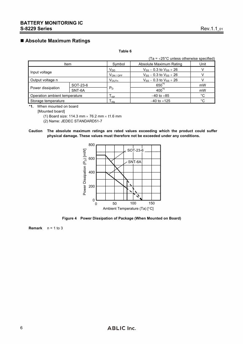
Absolute Maximum Ratings
Table 6
(Ta = 25°C unless otherwise specified)
Item Symbol Absolute Maximum Rating Unit
Input voltage VDD VSS 0.3 to VSS 26 V
VON / OFF VSS 0.3 to VSS 26 V
Output voltage n VOUTn VSS 0.3 to VSS 26 V
Power dissipation SOT-23-6
PD 650*1 mW
SNT-6A 400*1 mW
Operation ambient temperature Topr 40 to 85 °C
Storage temperature Tstg 40 to 125 °C
*1. When mounted on board [Mounted board]
(1) Board size: 114.3 mm 76.2 mm t1.6 mm (2) Name: JEDEC STANDARD51-7
Caution The absolute maximum ratings are rated values exceeding which the product could suffer
physical damage. These values must therefore not be exceeded under any conditions.
0 50 100 150
800
0
Pow
er D
issi
patio
n (P
D)
[mW
]
Ambient Temperature (Ta) [C]
SOT-23-6
400
600
200
SNT-6A
Figure 4 Power Dissipation of Package (When Mounted on Board)
Remark n = 1 to 3
BATTERY MONITORING IC Rev.1.1_01 S-8229 Series
7
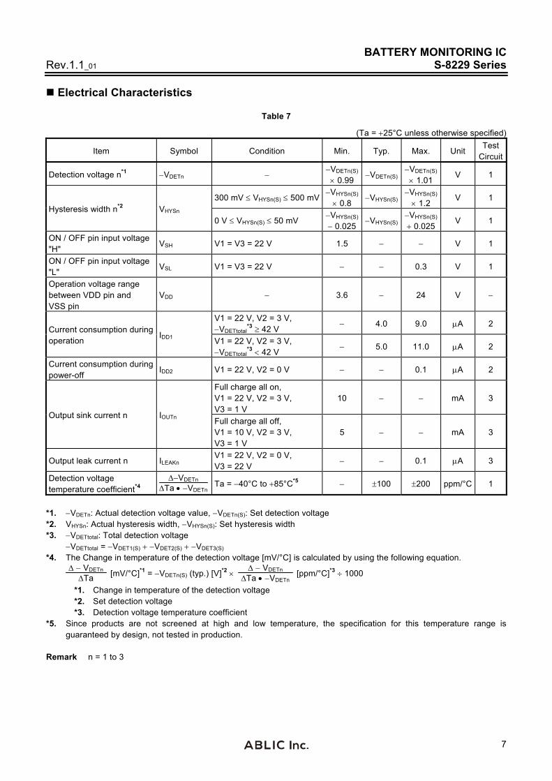
Electrical Characteristics
Table 7
(Ta = 25°C unless otherwise specified)
Item Symbol Condition Min. Typ. Max. Unit Test
Circuit
Detection voltage n*1 VDETn VDETn(S) 0.99
VDETn(S) VDETn(S) 1.01
V 1
Hysteresis width n*2 VHYSn 300 mV VHYSn(S) 500 mV
VHYSn(S) 0.8
VHYSn(S) VHYSn(S) 1.2
V 1
0 V VHYSn(S) 50 mV VHYSn(S) 0.025
VHYSn(S) VHYSn(S) 0.025
V 1
ON / OFF pin input voltage "H"
VSH V1 = V3 = 22 V 1.5 V 1
ON / OFF pin input voltage "L"
VSL V1 = V3 = 22 V 0.3 V 1
Operation voltage range between VDD pin and VSS pin
VDD 3.6 24 V
Current consumption during operation
IDD1
V1 = 22 V, V2 = 3 V, VDETtotal
*3 42 V 4.0 9.0 A 2
V1 = 22 V, V2 = 3 V, VDETtotal
*3 42 V 5.0 11.0 A 2
Current consumption during power-off
IDD2 V1 = 22 V, V2 = 0 V 0.1 A 2
Output sink current n IOUTn
Full charge all on, V1 = 22 V, V2 = 3 V, V3 = 1 V
10 mA 3
Full charge all off, V1 = 10 V, V2 = 3 V, V3 = 1 V
5 mA 3
Output leak current n ILEAKn V1 = 22 V, V2 = 0 V, V3 = 22 V
0.1 A 3
Detection voltage temperature coefficient*4
VDETn
Ta VDETn Ta = 40°C to 85°C*5 100 200 ppm/°C 1
*1. VDETn: Actual detection voltage value, VDETn(S): Set detection voltage *2. VHYSn: Actual hysteresis width, VHYSn(S): Set hysteresis width *3. VDETtotal: Total detection voltage VDETtotal = VDET1(S) VDET2(S) VDET3(S) *4. The Change in temperature of the detection voltage [mV/°C] is calculated by using the following equation.
VDETn
Ta [mV/°C]*1 = VDETn(S) (typ.) [V]*2
VDETn
Ta VDETn [ppm/°C]*3 1000
*1. Change in temperature of the detection voltage *2. Set detection voltage *3. Detection voltage temperature coefficient
*5. Since products are not screened at high and low temperature, the specification for this temperature range is guaranteed by design, not tested in production.
Remark n = 1 to 3
BATTERY MONITORING IC S-8229 Series Rev.1.1_01
8
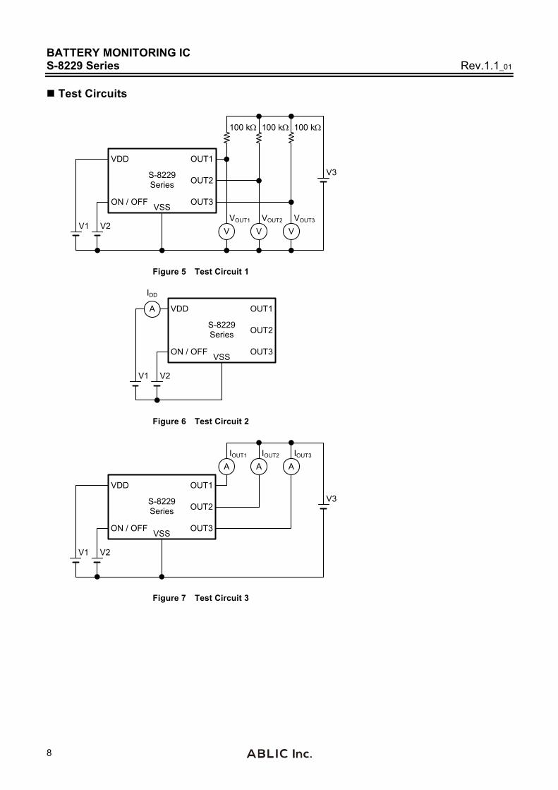
Test Circuits
OUT1
OUT2
OUT3
S-8229 Series
VSS
V2 V1 VOUT1 VOUT2 VOUT3
V3
V V V
100 k 100 k 100 k
ON / OFF
VDD
Figure 5 Test Circuit 1
OUT1
OUT2
OUT3
S-8229 Series
VSS
V2 V1
ON / OFF
VDD A
IDD
Figure 6 Test Circuit 2
OUT1
OUT2
OUT3
S-8229 Series
ON / OFF
VSS
VDD
V2 V1
IOUT1
A A
IOUT2
A
IOUT3
V3
Figure 7 Test Circuit 3

BATTERY MONITORING IC Rev.1.1_01 S-8229 Series
9
Standard Circuit
OUT1
OUT2
OUT3
S-8229 Series
ON / OFF
VSS
VDD
ROUT1 ROUT2 ROUT3
R1
C1
Figure 8
Table 8 Constants for External Components
Symbol Purpose Typ. Remark
R1*1 For power fluctuation 470 Set the value as small as possible to prevent deterioration of the detection voltage.
C1 For power fluctuation 0.1 F Set R1 C1 40 106.
ROUTn*2 For output pin pull-up 100 k
Make sure the power dissipation of the S-8229 Series is not exceeded.
*1. Set up R1 as 100 k or less to prevent oscillation. *2. Set up each of ROUTn as 620 or more so that the power dissipation is not exceeded. Caution The above connection diagram and constant will not guarantee successful operation. Perform thorough
evaluation using the actual application to set the constant. Remark n = 1 to 3

BATTERY MONITORING IC S-8229 Series Rev.1.1_01
10
Operation
1. Basic operation
The basic operation when VON / OFF VSH is shown as follows. 1. 1 When the power supply voltage (VDD) increases
The OUTn pin becomes release status if VDD is equal to or higher than the release voltage (VDETn).
Table 9 Set Conditions at Releasing
Output Logic VOUTn Nch n
Full charge all on VSS OnFull charge all off High-Z Off
1. 2 When VDD decreases
The OUTn pin becomes detection status if VDD is equal to or lower than the detection voltage (VDETn).
Table 10 Set Conditions at Detecting
Output Logic VOUTn Nch n
Full charge all on High-Z OffFull charge all off VSS On
1. 3 When VDD minimum operation voltage
The OUTn pin voltage is indefinite.
Remark n = 1 to 3
2. ON / OFF pin
This pin starts and stops the S-8229 Series. When VON / OFF is set to VSL or lower, the entire internal circuit stops operating, and Nch n (refer to Figure 1 in " Block Diagram") is turned off, reducing current consumption significantly. The ON / OFF pin is configured as shown in Figure 9. The ON / OFF pin is not internally pulled up or pulled down, so do not use the ON / OFF pin in the floating status. When not using the ON / OFF pin, connect the pin to the VDD pin.
ON / OFF
VDD
VSS
Figure 9
Remark n = 1 to 3

BATTERY MONITORING IC Rev.1.1_01 S-8229 Series
11
Timing Charts
1. Nch open-drain output (full charge all on, VON / OFF VSH)
VDET1
VDD pin voltage
OUT2 pin voltage
High-Z
VSS
VDET1
VDET2
VDET2
VDET3
VDET3
High-Z
VSS
High-Z
VSS
Minimum operation voltage
OUT1 pin voltage
OUT3 pin voltage
Figure 10
Remark When VDD is equal to or lower than the minimum operation voltage, the output voltage from the OUT1 pin to the OUT3 pin is indefinite in the shaded area.
BATTERY MONITORING IC S-8229 Series Rev.1.1_01
12
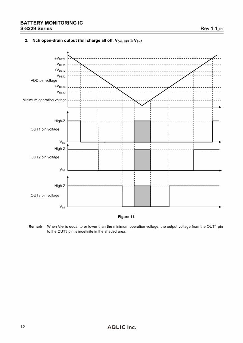
2. Nch open-drain output (full charge all off, VON / OFF VSH)
VDET1
VDD pin voltage
OUT2 pin voltage
High-Z
VSS
VDET1
VDET2
VDET2
VDET3
VDET3
High-Z
VSS
High-Z
VSS
Minimum operation voltage
OUT1 pin voltage
OUT3 pin voltage
Figure 11
Remark When VDD is equal to or lower than the minimum operation voltage, the output voltage from the OUT1 pin to the OUT3 pin is indefinite in the shaded area.

BATTERY MONITORING IC Rev.1.1_01 S-8229 Series
13
Application Circuits
1. Detection of residual quantity of the battery used by LED
OUT1
OUT2
OUT3
S-8229 Series
ON / OFF
VSS
VDD
ROUT1 ROUT2 ROUT3
LED3 LED2 LED1 R1
C1
Figure 12
Caution The above connection diagram and constant will not guarantee successful operation. Perform thorough evaluation using the actual application to set the constant.
2. Change of detection voltage
When the detection voltage is changed by using a resistance divider, set RA 100 k to prevent oscillation, as shown in Figure 13. The detection voltage after changing is calculated by using the following equation.
Detection voltage = RA RB
RB VDETn RA IDD
OUT1
OUT2
OUT3
S-8229 Series
ON / OFF
VSS
VDD
RA
RB
ROUT1 ROUT2 ROUT3
C1
Figure 13
Caution 1. Note that the detection voltage may deviate from the value determined by the ratio of RA and RB
in the case of the above connection diagram. 2. The above connection diagram and constant will not guarantee successful operation. Perform
thorough evaluation using the actual application to set the constant.
Remark n = 1 to 3
BATTERY MONITORING IC S-8229 Series Rev.1.1_01
14
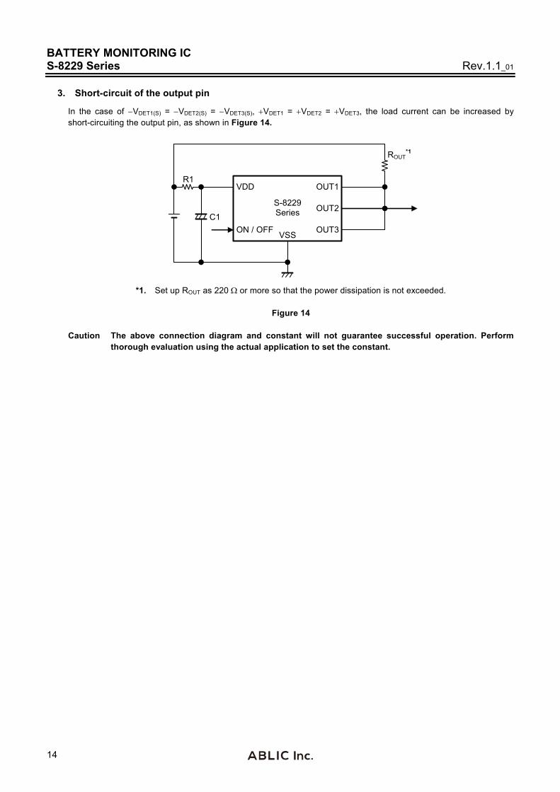
3. Short-circuit of the output pin
In the case of VDET1(S) = VDET2(S) = VDET3(S), VDET1 = VDET2 = VDET3, the load current can be increased by short-circuiting the output pin, as shown in Figure 14.
OUT1
OUT2
OUT3
S-8229 Series
ON / OFF
VSS
VDD
ROUT*1
C1
R1
*1. Set up ROUT as 220 or more so that the power dissipation is not exceeded.
Figure 14
Caution The above connection diagram and constant will not guarantee successful operation. Perform thorough evaluation using the actual application to set the constant.

BATTERY MONITORING IC Rev.1.1_01 S-8229 Series
15
Precautions
The application conditions for the input voltage, output voltage, and output pin pull-up resistance should not exceed the package power dissipation.
Wiring patterns for the VDD pin, the VOUT pin and the VSS pin should be designed so that the impedance is low. Note that the detection voltage may deviate due to the resistance component of output sink current and the VSS pin
wiring. In applications where a resistor is connected to the input (refer to Figure 8 in " Standard Circuit"), the
feed-through current which is generated when the output switches causes a voltage drop equal to feed-through current input resistance. In this state, the feed-through current stops and its resultant voltage drop disappears, and the output switches. The feed-through current is then generated again, a voltage drop appears. Note that an oscillation may be generated for this reason.
When designing for mass production using an application circuit described herein, the product deviation and
temperature characteristics should be taken into consideration. ABLIC Inc. shall not bear any responsibility for patent infringements related to products using the circuits described herein.
Do not apply an electrostatic discharge to this IC that exceeds the performance ratings of the built-in electrostatic
protection circuit. ABLIC Inc. claims no responsibility for any disputes arising out of or in connection with any infringement by
products including this IC of patents owned by a third party.
BATTERY MONITORING IC S-8229 Series Rev.1.1_01
16
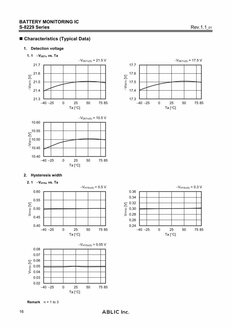
Characteristics (Typical Data)
1. Detection voltage
1. 1 VDETn vs. Ta VDETn(S) = 21.5 V VDETn(S) = 17.5 V
−VD
ETn
[V]
21.3
21.4
21.5
21.6
21.7
−40 0 25 50 75 85−25Ta [°C]
−VD
ETn
[V]
17.3
17.4
17.5
17.6
17.7
−40 0 25 50 75 85−25Ta [°C]
VDETn(S) = 10.5 V
−VD
ETn
[V]
10.40
10.45
10.50
10.55
10.60
−40 0 25 50 75 85−25Ta [°C]
2. Hysteresis width
2. 1 VHYSn vs. Ta VHYSn(S) = 0.5 V VHYSn(S) = 0.3 V
VH
YS
n [V
]
0.40
0.45
0.50
0.55
0.60
−40 0 25 50 75 85−25Ta [°C]
VH
YS
n [V
]
0.240.260.280.30
0.340.32
0.36
−40 0 25 50 75 85−25Ta [°C]
VHYSn(S) = 0.05 V
VH
YS
n [V
]
0.020.030.040.05
0.070.06
0.08
−40 0 25 50 75 85−25Ta [°C]
Remark n = 1 to 3
BATTERY MONITORING IC Rev.1.1_01 S-8229 Series
17
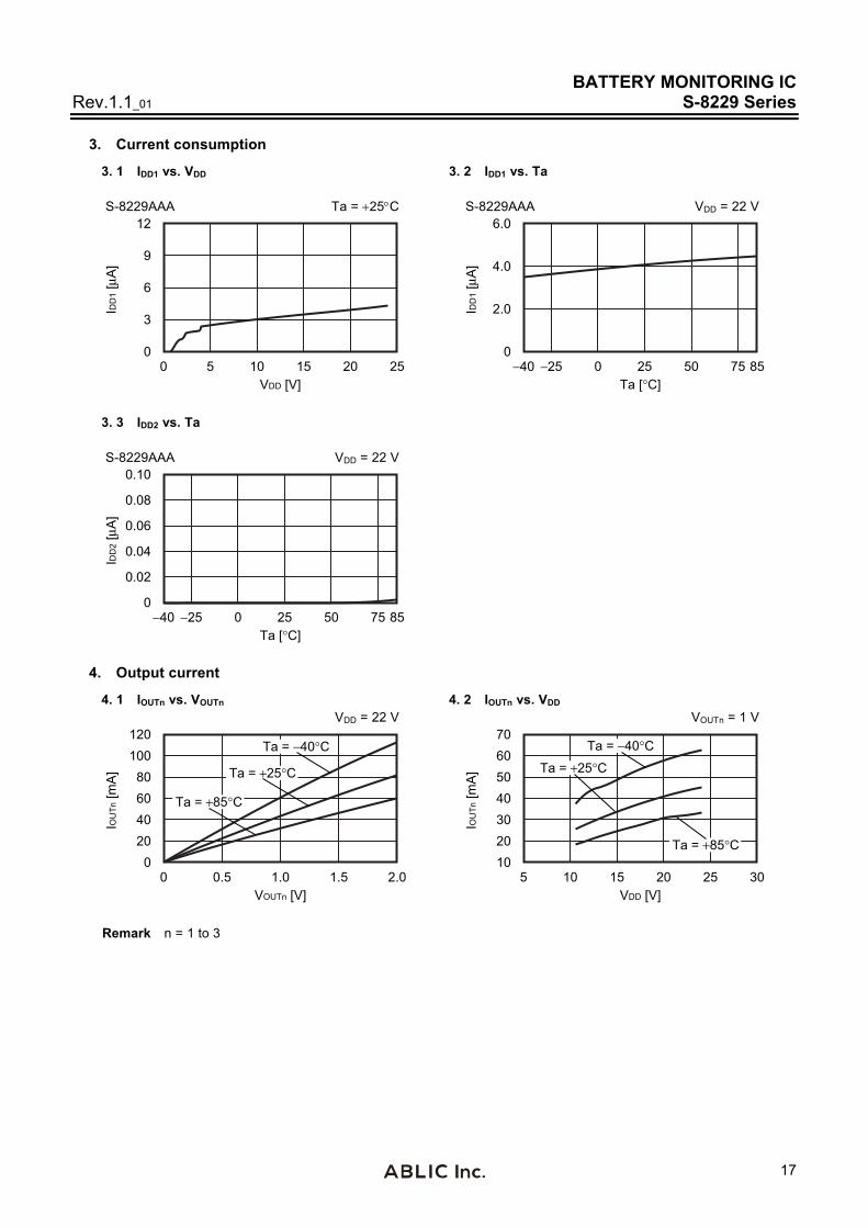
3. Current consumption
3. 1 IDD1 vs. VDD 3. 2 IDD1 vs. Ta
S-8229AAA Ta = 25C S-8229AAA VDD = 22 V
IDD
1 [μA
]
0
6
3
9
12
0 5 10 15 20 25VDD [V]
IDD
1 [μA
]
0
2.0
4.0
6.0
−40 0 25 50 75 85−25Ta [°C]
3. 3 IDD2 vs. Ta
S-8229AAA VDD = 22 V
IDD
2 [μA
]
0
0.02
0.06
0.08
0.04
0.10
−40 0 25 50 75 85−25Ta [°C]
4. Output current
4. 1 IOUTn vs. VOUTn 4. 2 IOUTn vs. VDD VDD = 22 V VOUTn = 1 V
IOU
Tn [m
A]
0
6080
2040
100120
0 0.5 1.0 1.5 2.0VOUTn [V]
Ta = −40°C
Ta = +25°C
Ta = +85°C
IOU
Tn [m
A]
10
3020
5040
7060
5 10 15 20 3025VDD [V]
Ta = −40°C
Ta = +25°C
Ta = +85°C
Remark n = 1 to 3
BATTERY MONITORING IC S-8229 Series Rev.1.1_01
18
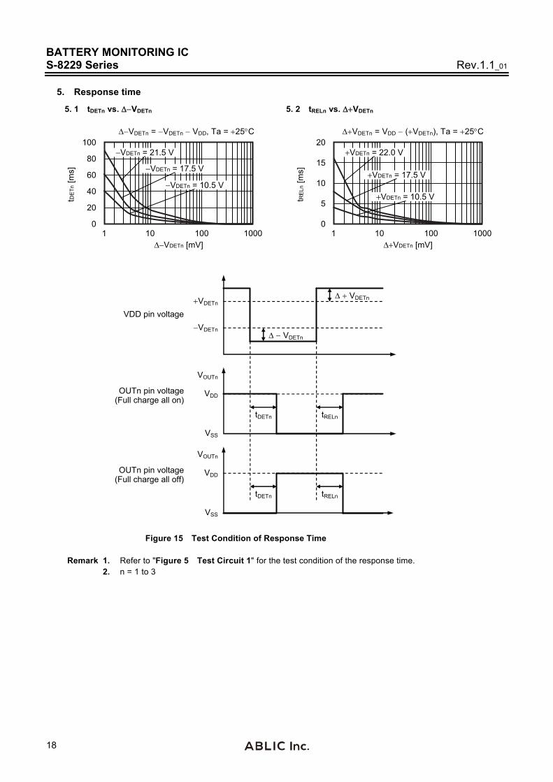
5. Response time
5. 1 tDETn vs. VDETn 5. 2 tRELn vs. VDETn
VDETn = VDETn VDD, Ta = 25C VDETn = VDD (VDETn), Ta = 25C
tDE
Tn [m
s]
0
40
80
60
20
100
1 100 100010Δ−VDETn [mV]
−VDETn = 21.5 V
−VDETn = 17.5 V
−VDETn = 10.5 V
tRE
Ln [m
s]
0
5
15
10
20
1 100 100010Δ+VDETn [mV]
+VDETn = 22.0 V
+VDETn = 17.5 V
+VDETn = 10.5 V
VDD
VSS
OUTn pin voltage (Full charge all off)
VOUTn
VDD
VSS
OUTn pin voltage (Full charge all on)
VOUTn
VDD pin voltage
VDETn
VDETn
tDETn
tDETn tRELn
tRELn
VDETn
VDETn
Figure 15 Test Condition of Response Time
Remark 1. Refer to "Figure 5 Test Circuit 1" for the test condition of the response time. 2. n = 1 to 3

BATTERY MONITORING IC Rev.1.1_01 S-8229 Series
19
Marking Specifications
1. SOT-23-6
1 2 3
46 5
Top view
(1) (2) (3) (4)
(1) to (3): Product code (Refer to Product name vs. Product code) (4): Lot number
Product name vs. Product code
Product Name Product Code
(1) (2) (3)
S-8229AAA-M6T1U Y S A
S-8229AAB-M6T1U Y S B
S-8229AAC-M6T1U Y S C
S-8229AAG-M6T1U Y S G
S-8229AAH-M6T1U Y S H
S-8229AAI-M6T1U Y S I
S-8229AAJ-M6T1U Y S J
S-8229AAK-M6T1U Y S K
2. SNT-6A
Top view
1 32
6 45
(1) (2) (3)
(4) (5) (6)
(1) to (3): Product code (Refer to Product name vs. Product code) (4) to (6): Lot number
Product name vs. Product code
Product Name Product Code
(1) (2) (3)
S-8229AAF-I6T1U Y S F

���
�����
���
����
������ ��
�� ����
����
�� ����
� � �
�� �
���������
�� �
�����������
�� �
��
�������������������
���������������
��������������� !"��!"
���
�����
���
����
������ ��
��
���
� � �
#���������
��������
#��������� �������
�������
��������
�������
�����������$�������
�������$�������
��������$%&& � & � �%'
( )�)�& *+��!
�������,���'�+*- ".��������/

���
�����
���
����
������ ��
��
�����%0�
������
#������
,��1/ ,��1/
2�3 �4���
�!5%&6 )�)&%7�!6��!�+- �* !+&%5�'%&+
�����������8�������
�������8�������
��������8 5
���
�����
���
����
������ ��
��
��������������������
��������� �����
������������� �����
��������
���������
��������������
���
��� ����!
� � !
���

���
�����
���
����
������ ��
"��#�#�$�%&���
���������������
�������
'�������
���
'������������ ���������
���������
��
�������(� �����
������()$$ ��$ � �)*�
�����������(� �����
����
���
��
�
!
� �

���
�����
���
����
������ ��
�����)+�
,�����!
'�!����
-��./ -��./
0�1�
�����������2� �����
�������2� �����
��3)$4�#�#$)5��4����&6��%��&$)3�*)$&
������2��3
�7����
��

���
�����
���
����
������ ��
��
�������������)�#�2�%�����#)&���
��������� ������������������ �����
��!���
����
��!�
����
�
�
��� ��� ������� ������������������ ������������������� ���������� ����������������� ���������
������ ����������� ��������������� ���� ���������� ���������� ����������������� ��!!"����������������� ���������� ����������
"�#� �� ������������ ������$���������� �������� ������ �� ���������� ���
%�&����� ��'()��*������+���,��-����'������� ����
��� -�������������@���!�����&<*�/��� �-��!�����A��������/
!!"���
()�
����)<�)&&��&����&��&6��3)�#�*)&&�$��5�#&6�-�������������@���!�����&<*�/���������&�5�#���&6��3)�#�*)&&�$��&��&6��%��&�$��:�&6��*)%?)4���-���!�����A���������/�
��
��� -��!�����A��������/
-�������������@���!�����&<*�/

Disclaimers (Handling Precautions)
1. All the information described herein (product data, specifications, figures, tables, programs, algorithms and application circuit examples, etc.) is current as of publishing date of this document and is subject to change without notice.
2. The circuit examples and the usages described herein are for reference only, and do not guarantee the success of any specific mass-production design. ABLIC Inc. is not responsible for damages caused by the reasons other than the products described herein (hereinafter "the products") or infringement of third-party intellectual property right and any other right due to the use of the information described herein.
3. ABLIC Inc. is not responsible for damages caused by the incorrect information described herein.
4. Be careful to use the products within their specified ranges. Pay special attention to the absolute maximum ratings, operation voltage range and electrical characteristics, etc. ABLIC Inc. is not responsible for damages caused by failures and / or accidents, etc. that occur due to the use of the products outside their specified ranges.
5. When using the products, confirm their applications, and the laws and regulations of the region or country where they are used and verify suitability, safety and other factors for the intended use.
6. When exporting the products, comply with the Foreign Exchange and Foreign Trade Act and all other export-related laws, and follow the required procedures.
7. The products must not be used or provided (exported) for the purposes of the development of weapons of mass destruction or military use. ABLIC Inc. is not responsible for any provision (export) to those whose purpose is to develop, manufacture, use or store nuclear, biological or chemical weapons, missiles, or other military use.
8. The products are not designed to be used as part of any device or equipment that may affect the human body, human life, or assets (such as medical equipment, disaster prevention systems, security systems, combustion control systems, infrastructure control systems, vehicle equipment, traffic systems, in-vehicle equipment, aviation equipment, aerospace equipment, and nuclear-related equipment), excluding when specified for in-vehicle use or other uses. Do not apply the products to the above listed devices and equipments without prior written permission by ABLIC Inc. Especially, the products cannot be used for life support devices, devices implanted in the human body and devices that directly affect human life, etc. Prior consultation with our sales office is required when considering the above uses. ABLIC Inc. is not responsible for damages caused by unauthorized or unspecified use of our products.
9. Semiconductor products may fail or malfunction with some probability. The user of the products should therefore take responsibility to give thorough consideration to safety design including redundancy, fire spread prevention measures, and malfunction prevention to prevent accidents causing injury or death, fires and social damage, etc. that may ensue from the products' failure or malfunction. The entire system must be sufficiently evaluated and applied on customer's own responsibility.
10. The products are not designed to be radiation-proof. The necessary radiation measures should be taken in the product design by the customer depending on the intended use.
11. The products do not affect human health under normal use. However, they contain chemical substances and heavy metals and should therefore not be put in the mouth. The fracture surfaces of wafers and chips may be sharp. Be careful when handling these with the bare hands to prevent injuries, etc.
12. When disposing of the products, comply with the laws and ordinances of the country or region where they are used.
13. The information described herein contains copyright information and know-how of ABLIC Inc. The information described herein does not convey any license under any intellectual property rights or any other rights belonging to ABLIC Inc. or a third party. Reproduction or copying of the information from this document or any part of this document described herein for the purpose of disclosing it to a third-party without the express permission of ABLIC Inc. is strictly prohibited.
14. For more details on the information described herein, contact our sales office.
2.2-2018.06
www.ablic.com