Embed Size (px)
Citation preview
RTL8763B Series RTL8763BM, RTL8763BF, RTL8763BFR, RTL8763BS, RTL8763BA
BLUETOOTH 5 DUAL MODE SOC
PRELIMINARY DATASHEET (CONFIDENTIAL: Development Partners Only)
Rev. 0.92
13rd
, November 2017
Track ID: JATR-8275-15
Realtek Semiconductor Corp. No. 2, Innovation Road II, Hsinchu Science Park, Hsinchu 300, Taiwan
Tel.: +886-3-578-0211. Fax: +886-3-577-6047
www.realtek.com
Realtek confidential files
The document authorized to
WTMEC
2017-11-16 13:21:21
RTL8763B Series
Datasheet Preliminary
Bluetooth 5 Dual Mode SOC ii Track ID: JATR-8275-15 Rev. 0.9
COPYRIGHT
©2017 Realtek Semiconductor Corp. All rights reserved. No part of this document may be reproduced,
transmitted, transcribed, stored in a retrieval system, or translated into any language in any form or by any
means without the written permission of Realtek Semiconductor Corp.
DISCLAIMER
Realtek provides this document ‘as is’, without warranty of any kind. Realtek may make improvements
and/or changes in this document or in the product described in this document at any time. This document
could include technical inaccuracies or typographical errors.
TRADEMARKS
Realtek is a trademark of Realtek Semiconductor Corporation. Other names mentioned in this document
are trademarks/registered trademarks of their respective owners.
LICENSE
This product is covered by one or more of the following patents: US5,307,459, US5,434,872,
US5,732,094, US6,570,884, US6,115,776, and US6,327,625.
USING THIS DOCUMENT
This document is intended for the software engineer’s reference and provides detailed programming
information.
Though every effort has been made to ensure that this document is current and accurate, more information
may have become available subsequent to the production of this guide.
ELECTROSTATIC DISCHARGE (ESD) WARNING
This product can be damaged by Electrostatic Discharge (ESD). When handling, care must be taken.
Damage due to inappropriate handling is not covered by warranty.
Do not open the protective conductive packaging until you have read the following, and are at an
approved anti-static workstation.
• Use an approved anti-static mat to cover your work surface.
• Use a conductive wrist strap attached to a good earth ground
• Always discharge yourself by touching a grounded bare metal surface or approved anti-static mat
before picking up an ESD-sensitive electronic component
• If working on a prototyping board, use a soldering iron or station that is marked as ESD-safe
• Always disconnect the microcontroller from the prototyping board when it is being worked on
REVISION HISTORY Revision Release Date Summary
0.92 2017/11/14 Preliminary Release.
Realtek confidential files
The document authorized to
WTMEC
2017-11-16 13:21:21
RTL8763B Series
Datasheet Preliminary
Bluetooth 5 Dual Mode SOC iii Track ID: JATR-8275-15 Rev. 0.9
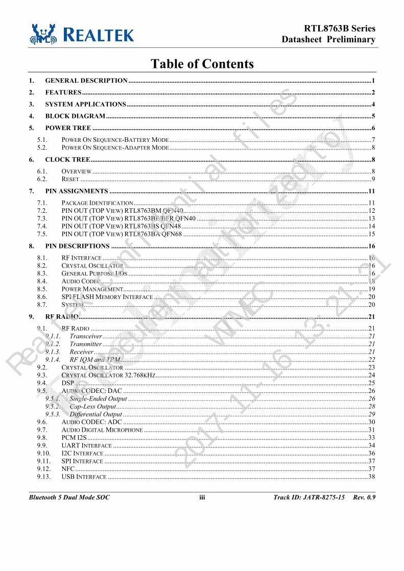
Table of Contents 1. GENERAL DESCRIPTION .............................................................................................................................................. 1
2. FEATURES ......................................................................................................................................................................... 2
3. SYSTEM APPLICATIONS ............................................................................................................................................... 4
4. BLOCK DIAGRAM ........................................................................................................................................................... 5
5. POWER TREE ................................................................................................................................................................... 6
5.1. POWER ON SEQUENCE-BATTERY MODE ...................................................................................................................... 7 5.2. POWER ON SEQUENCE-ADAPTER MODE ...................................................................................................................... 8
6. CLOCK TREE .................................................................................................................................................................... 8
6.1. OVERVIEW ................................................................................................................................................................... 8 6.2. RESET .......................................................................................................................................................................... 9
7. PIN ASSIGNMENTS ....................................................................................................................................................... 11
7.1. PACKAGE IDENTIFICATION ......................................................................................................................................... 11 7.2. PIN OUT (TOP VIEW) RTL8763BM QFN40............................................................................................................ 12 7.3. PIN OUT (TOP VIEW) RTL8763BF/BFR QFN40 .................................................................................................... 13 7.4. PIN OUT (TOP VIEW) RTL8763BS QFN48 ............................................................................................................. 14 7.5. PIN OUT (TOP VIEW) RTL8763BA QFN68 ............................................................................................................ 15
8. PIN DESCRIPTIONS ...................................................................................................................................................... 16
8.1. RF INTERFACE ........................................................................................................................................................... 16 8.2. CRYSTAL OSCILLATOR .............................................................................................................................................. 16 8.3. GENERAL PURPOSE I/OS ............................................................................................................................................ 16 8.4. AUDIO CODEC ............................................................................................................................................................ 18 8.5. POWER MANAGEMENT ............................................................................................................................................... 19 8.6. SPI FLASH MEMORY INTERFACE ............................................................................................................................. 20 8.7. SYSTEM ...................................................................................................................................................................... 20
9. RF RADIO ......................................................................................................................................................................... 21
9.1. RF RADIO .................................................................................................................................................................. 21 9.1.1. Transceiver ........................................................................................................................................................... 21 9.1.2. Transmitter ........................................................................................................................................................... 21 9.1.3. Receiver ................................................................................................................................................................ 21 9.1.4. RF IQM and TPM ................................................................................................................................................. 22
9.2. CRYSTAL OSCILLATOR .............................................................................................................................................. 23 9.3. CRYSTAL OSCILLATOR 32.768KHZ ............................................................................................................................ 24 9.4. DSP ........................................................................................................................................................................... 25 9.5. AUDIO CODEC: DAC ............................................................................................................................................... 26
9.5.1. Single-Ended Output ............................................................................................................................................ 26 9.5.2. Cap-Less Output ................................................................................................................................................... 28 9.5.3. Differential Output ............................................................................................................................................... 29
9.6. AUDIO CODEC: ADC ............................................................................................................................................... 30 9.7. AUDIO DIGITAL MICROPHONE ................................................................................................................................... 31 9.8. PCM I2S .................................................................................................................................................................... 33 9.9. UART INTERFACE ..................................................................................................................................................... 34 9.10. I2C INTERFACE .......................................................................................................................................................... 36 9.11. SPI INTERFACE .......................................................................................................................................................... 37 9.12. NFC ........................................................................................................................................................................... 37 9.13. USB INTERFACE ........................................................................................................................................................ 38
Realtek confidential files
The document authorized to
WTMEC
2017-11-16 13:21:21
RTL8763B Series
Datasheet Preliminary
Bluetooth 5 Dual Mode SOC iv Track ID: JATR-8275-15 Rev. 0.9
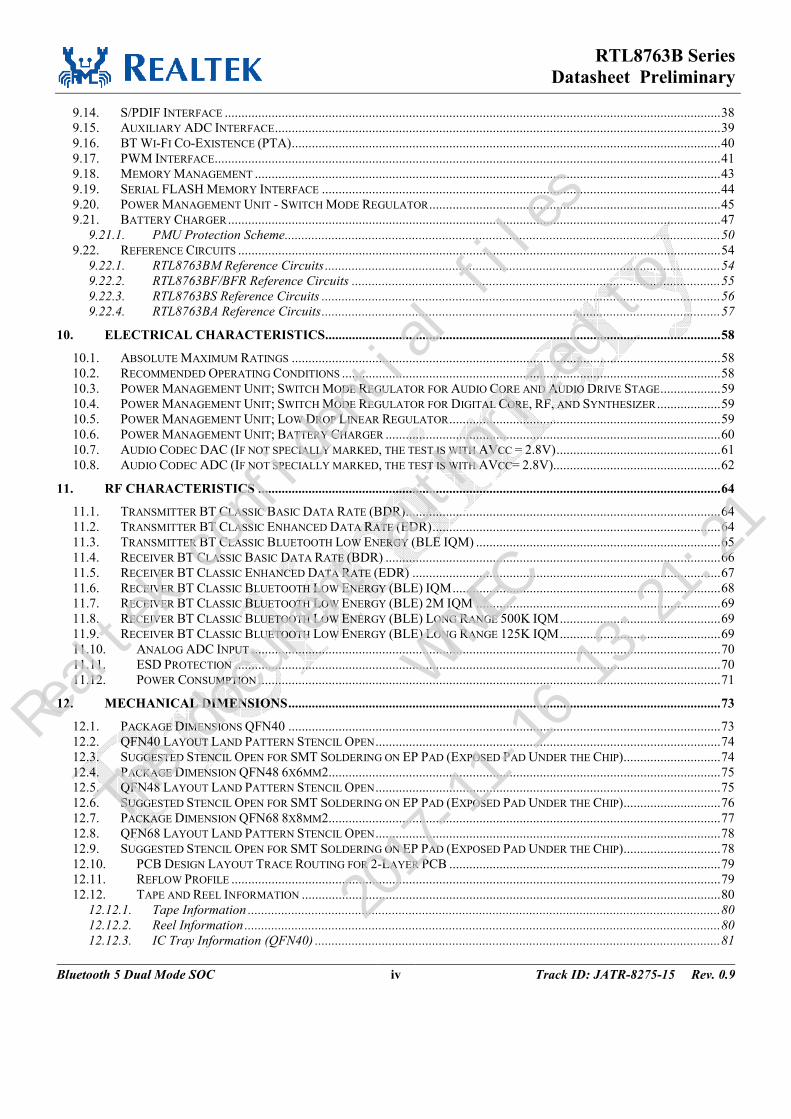
9.14. S/PDIF INTERFACE .................................................................................................................................................... 38 9.15. AUXILIARY ADC INTERFACE ..................................................................................................................................... 39 9.16. BT WI-FI CO-EXISTENCE (PTA) ................................................................................................................................ 40 9.17. PWM INTERFACE ....................................................................................................................................................... 41 9.18. MEMORY MANAGEMENT ........................................................................................................................................... 43 9.19. SERIAL FLASH MEMORY INTERFACE ....................................................................................................................... 44 9.20. POWER MANAGEMENT UNIT - SWITCH MODE REGULATOR ....................................................................................... 45 9.21. BATTERY CHARGER ................................................................................................................................................... 47
9.21.1. PMU Protection Scheme .................................................................................................................................. 50 9.22. REFERENCE CIRCUITS ................................................................................................................................................ 54
9.22.1. RTL8763BM Reference Circuits ...................................................................................................................... 54 9.22.2. RTL8763BF/BFR Reference Circuits .............................................................................................................. 55 9.22.3. RTL8763BS Reference Circuits ....................................................................................................................... 56 9.22.4. RTL8763BA Reference Circuits ....................................................................................................................... 57
10. ELECTRICAL CHARACTERISTICS...................................................................................................................... 58
10.1. ABSOLUTE MAXIMUM RATINGS ................................................................................................................................ 58 10.2. RECOMMENDED OPERATING CONDITIONS ................................................................................................................. 58 10.3. POWER MANAGEMENT UNIT; SWITCH MODE REGULATOR FOR AUDIO CORE AND AUDIO DRIVE STAGE .................. 59 10.4. POWER MANAGEMENT UNIT; SWITCH MODE REGULATOR FOR DIGITAL CORE, RF, AND SYNTHESIZER ................... 59 10.5. POWER MANAGEMENT UNIT; LOW DROP LINEAR REGULATOR ................................................................................. 59 10.6. POWER MANAGEMENT UNIT; BATTERY CHARGER .................................................................................................... 60 10.7. AUDIO CODEC DAC (IF NOT SPECIALLY MARKED, THE TEST IS WITH AVCC = 2.8V) ................................................. 61 10.8. AUDIO CODEC ADC (IF NOT SPECIALLY MARKED, THE TEST IS WITH AVCC= 2.8V).................................................. 62
11. RF CHARACTERISTICS .......................................................................................................................................... 64
11.1. TRANSMITTER BT CLASSIC BASIC DATA RATE (BDR) .............................................................................................. 64 11.2. TRANSMITTER BT CLASSIC ENHANCED DATA RATE (EDR) ...................................................................................... 64 11.3. TRANSMITTER BT CLASSIC BLUETOOTH LOW ENERGY (BLE IQM) ......................................................................... 65 11.4. RECEIVER BT CLASSIC BASIC DATA RATE (BDR) .................................................................................................... 66 11.5. RECEIVER BT CLASSIC ENHANCED DATA RATE (EDR) ............................................................................................ 67 11.6. RECEIVER BT CLASSIC BLUETOOTH LOW ENERGY (BLE) IQM ................................................................................ 68 11.7. RECEIVER BT CLASSIC BLUETOOTH LOW ENERGY (BLE) 2M IQM ......................................................................... 69 11.8. RECEIVER BT CLASSIC BLUETOOTH LOW ENERGY (BLE) LONG RANGE 500K IQM ................................................ 69 11.9. RECEIVER BT CLASSIC BLUETOOTH LOW ENERGY (BLE) LONG RANGE 125K IQM ................................................ 69 11.10. ANALOG ADC INPUT ............................................................................................................................................ 70 11.11. ESD PROTECTION ................................................................................................................................................. 70 11.12. POWER CONSUMPTION .......................................................................................................................................... 71
12. MECHANICAL DIMENSIONS ................................................................................................................................. 73
12.1. PACKAGE DIMENSIONS QFN40 ................................................................................................................................. 73 12.2. QFN40 LAYOUT LAND PATTERN STENCIL OPEN ....................................................................................................... 74 12.3. SUGGESTED STENCIL OPEN FOR SMT SOLDERING ON EP PAD (EXPOSED PAD UNDER THE CHIP)............................. 74 12.4. PACKAGE DIMENSION QFN48 6X6MM2 ..................................................................................................................... 75 12.5. QFN48 LAYOUT LAND PATTERN STENCIL OPEN ....................................................................................................... 75 12.6. SUGGESTED STENCIL OPEN FOR SMT SOLDERING ON EP PAD (EXPOSED PAD UNDER THE CHIP)............................. 76 12.7. PACKAGE DIMENSION QFN68 8X8MM2 ..................................................................................................................... 77 12.8. QFN68 LAYOUT LAND PATTERN STENCIL OPEN ....................................................................................................... 78 12.9. SUGGESTED STENCIL OPEN FOR SMT SOLDERING ON EP PAD (EXPOSED PAD UNDER THE CHIP)............................. 78 12.10. PCB DESIGN LAYOUT TRACE ROUTING FOR 2-LAYER PCB ................................................................................. 79 12.11. REFLOW PROFILE .................................................................................................................................................. 79 12.12. TAPE AND REEL INFORMATION ............................................................................................................................. 80
12.12.1. Tape Information ............................................................................................................................................. 80 12.12.2. Reel Information .............................................................................................................................................. 80 12.12.3. IC Tray Information (QFN40) ......................................................................................................................... 81
Realtek confidential files
The document authorized to
WTMEC
2017-11-16 13:21:21
RTL8763B Series
Datasheet Preliminary
Bluetooth 5 Dual Mode SOC v Track ID: JATR-8275-15 Rev. 0.9
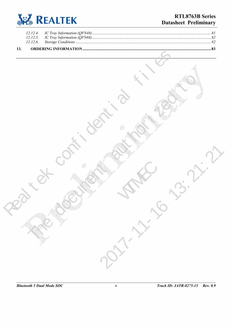
12.12.4. IC Tray Information (QFN48) ......................................................................................................................... 81 12.12.5. IC Tray Information (QFN68) ......................................................................................................................... 82 12.12.6. Storage Conditions .......................................................................................................................................... 82
13. ORDERING INFORMATION ................................................................................................................................... 83
Realtek confidential files
The document authorized to
WTMEC
2017-11-16 13:21:21
RTL8763B Series
Datasheet Preliminary
Bluetooth 5 Dual Mode SOC vi Track ID: JATR-8275-15 Rev. 0.9
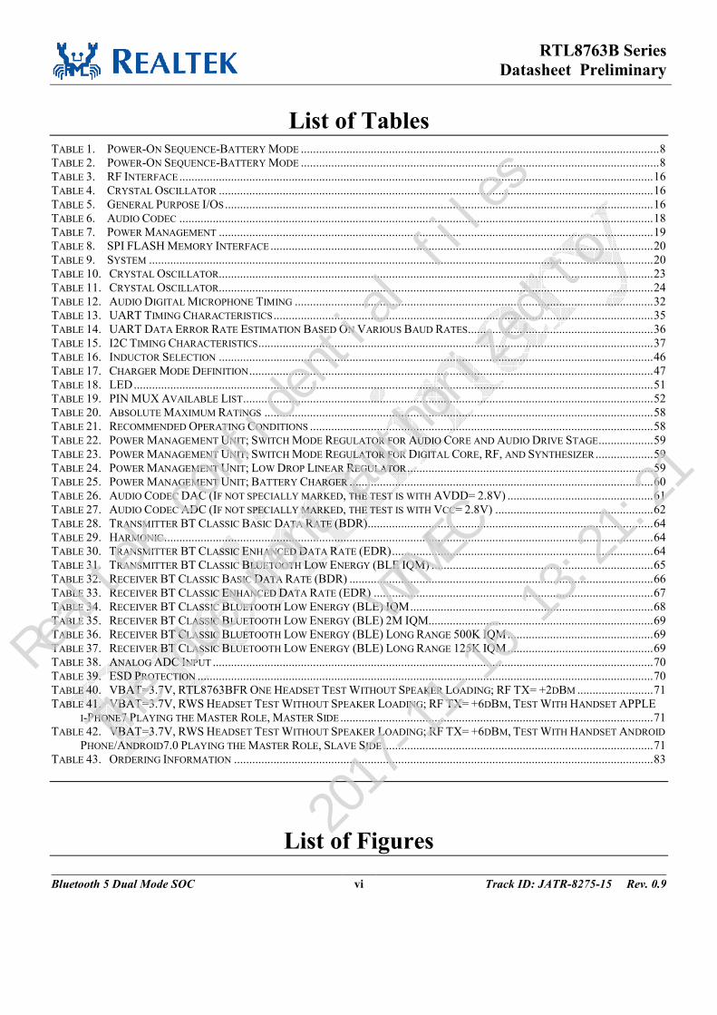
List of Tables TABLE 1. POWER-ON SEQUENCE-BATTERY MODE ...................................................................................................................... 8 TABLE 2. POWER-ON SEQUENCE-BATTERY MODE ...................................................................................................................... 8 TABLE 3. RF INTERFACE ............................................................................................................................................................ 16 TABLE 4. CRYSTAL OSCILLATOR ............................................................................................................................................... 16 TABLE 5. GENERAL PURPOSE I/OS ............................................................................................................................................. 16 TABLE 6. AUDIO CODEC ............................................................................................................................................................ 18 TABLE 7. POWER MANAGEMENT ............................................................................................................................................... 19 TABLE 8. SPI FLASH MEMORY INTERFACE .............................................................................................................................. 20 TABLE 9. SYSTEM ...................................................................................................................................................................... 20 TABLE 10. CRYSTAL OSCILLATOR............................................................................................................................................... 23 TABLE 11. CRYSTAL OSCILLATOR............................................................................................................................................... 24 TABLE 12. AUDIO DIGITAL MICROPHONE TIMING ...................................................................................................................... 32 TABLE 13. UART TIMING CHARACTERISTICS ............................................................................................................................. 35 TABLE 14. UART DATA ERROR RATE ESTIMATION BASED ON VARIOUS BAUD RATES ............................................................. 36 TABLE 15. I2C TIMING CHARACTERISTICS .................................................................................................................................. 37 TABLE 16. INDUCTOR SELECTION ............................................................................................................................................... 46 TABLE 17. CHARGER MODE DEFINITION ..................................................................................................................................... 47 TABLE 18. LED ........................................................................................................................................................................... 51 TABLE 19. PIN MUX AVAILABLE LIST ....................................................................................................................................... 52 TABLE 20. ABSOLUTE MAXIMUM RATINGS ................................................................................................................................ 58 TABLE 21. RECOMMENDED OPERATING CONDITIONS ................................................................................................................. 58 TABLE 22. POWER MANAGEMENT UNIT; SWITCH MODE REGULATOR FOR AUDIO CORE AND AUDIO DRIVE STAGE .................. 59 TABLE 23. POWER MANAGEMENT UNIT; SWITCH MODE REGULATOR FOR DIGITAL CORE, RF, AND SYNTHESIZER ................... 59 TABLE 24. POWER MANAGEMENT UNIT; LOW DROP LINEAR REGULATOR ................................................................................. 59 TABLE 25. POWER MANAGEMENT UNIT; BATTERY CHARGER .................................................................................................... 60 TABLE 26. AUDIO CODEC DAC (IF NOT SPECIALLY MARKED, THE TEST IS WITH AVDD= 2.8V) ................................................ 61 TABLE 27. AUDIO CODEC ADC (IF NOT SPECIALLY MARKED, THE TEST IS WITH VCC= 2.8V) .................................................... 62 TABLE 28. TRANSMITTER BT CLASSIC BASIC DATA RATE (BDR) .............................................................................................. 64 TABLE 29. HARMONIC ................................................................................................................................................................. 64 TABLE 30. TRANSMITTER BT CLASSIC ENHANCED DATA RATE (EDR) ...................................................................................... 64 TABLE 31. TRANSMITTER BT CLASSIC BLUETOOTH LOW ENERGY (BLE IQM) ......................................................................... 65 TABLE 32. RECEIVER BT CLASSIC BASIC DATA RATE (BDR) .................................................................................................... 66 TABLE 33. RECEIVER BT CLASSIC ENHANCED DATA RATE (EDR) ............................................................................................ 67 TABLE 34. RECEIVER BT CLASSIC BLUETOOTH LOW ENERGY (BLE) IQM ................................................................................ 68 TABLE 35. RECEIVER BT CLASSIC BLUETOOTH LOW ENERGY (BLE) 2M IQM.......................................................................... 69 TABLE 36. RECEIVER BT CLASSIC BLUETOOTH LOW ENERGY (BLE) LONG RANGE 500K IQM ................................................ 69 TABLE 37. RECEIVER BT CLASSIC BLUETOOTH LOW ENERGY (BLE) LONG RANGE 125K IQM ................................................ 69 TABLE 38. ANALOG ADC INPUT ................................................................................................................................................. 70 TABLE 39. ESD PROTECTION ...................................................................................................................................................... 70 TABLE 40. VBAT=3.7V, RTL8763BFR ONE HEADSET TEST WITHOUT SPEAKER LOADING; RF TX= +2DBM ......................... 71 TABLE 41. VBAT=3.7V, RWS HEADSET TEST WITHOUT SPEAKER LOADING; RF TX= +6DBM, TEST WITH HANDSET APPLE
I-PHONE7 PLAYING THE MASTER ROLE, MASTER SIDE ....................................................................................................... 71 TABLE 42. VBAT=3.7V, RWS HEADSET TEST WITHOUT SPEAKER LOADING; RF TX= +6DBM, TEST WITH HANDSET ANDROID
PHONE/ANDROID7.0 PLAYING THE MASTER ROLE, SLAVE SIDE ......................................................................................... 71 TABLE 43. ORDERING INFORMATION .......................................................................................................................................... 83
List of Figures
Realtek confidential files
The document authorized to
WTMEC
2017-11-16 13:21:21
RTL8763B Series
Datasheet Preliminary
Bluetooth 5 Dual Mode SOC vii Track ID: JATR-8275-15 Rev. 0.9
FIGURE 1. BLOCK DIAGRAM ........................................................................................................................................................ 5 FIGURE 2. POWER TREE-1 ............................................................................................................................................................ 6 FIGURE 3. POWER TREE-2 ............................................................................................................................................................ 7 FIGURE 4. POWER-ON SEQUENCE-BATTERY MODE ..................................................................................................................... 7 FIGURE 5. POWER-ON SEQUENCE-ADAPTER MODE ..................................................................................................................... 8 FIGURE 6. CLOCK TREE ................................................................................................................................................................ 9 FIGURE 7. RESET ........................................................................................................................................................................ 10 FIGURE 8. PACKAGE IDENTIFICATION ........................................................................................................................................ 11 FIGURE 9. PIN OUT (TOP VIEW) RTL8763BM QFN40 ........................................................................................................... 12 FIGURE 10. PIN OUT (TOP VIEW) RTL8763BF/BFR QFN40 ................................................................................................... 13 FIGURE 11. PIN OUT (TOP VIEW) RTL8763BS QFN48 ............................................................................................................ 14 FIGURE 12. PIN OUT (TOP VIEW) RTL8763BA QFN68 ........................................................................................................... 15 FIGURE 13. RF RADIO ................................................................................................................................................................. 21 FIGURE 14. REFERENCE CIRCUIT ................................................................................................................................................. 22 FIGURE 15. 40MHZ CRYSTAL SPECIFICATION SUGGESTION ....................................................................................................... 23 FIGURE 16. 32MHZ CRYSTAL SPECIFICATION SUGGESTION ....................................................................................................... 24 FIGURE 17. DSP INTERFACES IN RTL86XX IC PLATFORM .......................................................................................................... 25 FIGURE 18. CODEC AND DAC BLOCK DIAGRAM ......................................................................................................................... 26 FIGURE 19. RTL8763B MONO .................................................................................................................................................. 27 FIGURE 20. RTL8763B STEREO................................................................................................................................................ 27 FIGURE 21. RTL8763B MONO .................................................................................................................................................. 28 FIGURE 22. RTL8763B STEREO................................................................................................................................................ 28 FIGURE 23. RTL8763B MONO .................................................................................................................................................. 29 FIGURE 24. RTL8763B STEREO................................................................................................................................................ 29 FIGURE 25. CODEC AND ADC BLOCK DIAGRAM ......................................................................................................................... 30 FIGURE 26. RTL8763B DUAL MICROPHONE REFERENCE ........................................................................................................... 30 FIGURE 27. RTL8763B ONE MICROPHONE AND ONE AUX-IN REFERENCE ............................................................................... 31 FIGURE 28. AUDIO DIGITAL MICROPHONE .................................................................................................................................. 31 FIGURE 29. AUDIO DIGITAL MICROPHONE TIMING DIAGRAM ..................................................................................................... 32 FIGURE 30. I2S CONNECTION; RTL8763B IN MASTER MODE ..................................................................................................... 33 FIGURE 31. I2S CONNECTION; RTL8763B IN SLAVE MODE........................................................................................................ 33 FIGURE 32. TIMING DIAGRAM-3 .................................................................................................................................................. 34 FIGURE 33. UART INTERFACE .................................................................................................................................................... 35 FIGURE 34. UART INTERFACE TIMING DIAGRAM ....................................................................................................................... 35 FIGURE 35. I2C INTERFACE TIMING DIAGRAM ............................................................................................................................ 37 FIGURE 36. NEAR FIELD COMMUNICATION ................................................................................................................................. 38 FIGURE 37. USB INTERFACE ....................................................................................................................................................... 38 FIGURE 38. BLUETOOTH SPEAKER APPLICATION ........................................................................................................................ 39 FIGURE 39. BLUETOOTH AUDIO RECEIVER APPLICATION ........................................................................................................... 39 FIGURE 40. AUXILIARY ADC INTERFACE APPLICATION ............................................................................................................. 40 FIGURE 41. BT WI-FI CO-EXISTENCE (PTA) .............................................................................................................................. 40 FIGURE 42. PWM INTERFACE ..................................................................................................................................................... 41 FIGURE 43. COMPLEMENTARY OUTPUT MODE ENABLED BUT NOT SET IN THE DEAD ZONE ...................................................... 42 FIGURE 44. MAXIMUM SETTING OF DEAD ZONE ......................................................................................................................... 43 FIGURE 45. DEAD ZONE IS LONGER THAN PWM HIGH LEVEL TIMER ........................................................................................ 43 FIGURE 46. DEAD ZONE IS LONGER THAN PWM LOW LEVEL TIMER ......................................................................................... 43 FIGURE 47. MEMORY MANAGEMENT .......................................................................................................................................... 44 FIGURE 48. SERIAL FLASH MEMORY; 1 AND 2-BIT MODE ......................................................................................................... 44 FIGURE 49. SERIAL FLASH MEMORY; 4-BIT MODE .................................................................................................................... 45 FIGURE 50. POWER MANAGEMENT UNIT - SWITCH MODE REGULATOR ...................................................................................... 45 FIGURE 51. INDUCTOR SELECTION .............................................................................................................................................. 46 FIGURE 52. BATTERY VOLTAGE VS. CHARGER CURRENT CURVE ............................................................................................... 48 FIGURE 53. AMBIENT DETECTION FOR BATTERY CHARGE PROTECTION ..................................................................................... 49 FIGURE 54. PMU PROTECTION SCHEME ...................................................................................................................................... 50 FIGURE 55. LED .......................................................................................................................................................................... 51
Realtek confidential files
The document authorized to
WTMEC
2017-11-16 13:21:21
RTL8763B Series
Datasheet Preliminary
Bluetooth 5 Dual Mode SOC viii Track ID: JATR-8275-15 Rev. 0.9
FIGURE 56. I/O MUX ................................................................................................................................................................... 52 FIGURE 57. RTL8763BM REFERENCE CIRCUITS......................................................................................................................... 54 FIGURE 58. RTL8763BF/BFR REFERENCE CIRCUITS ................................................................................................................. 55 FIGURE 59. RTL8763BS REFERENCE CIRCUITS .......................................................................................................................... 56 FIGURE 60. RTL8763BS REFERENCE CIRCUITS .......................................................................................................................... 57
Realtek confidential files
The document authorized to
WTMEC
2017-11-16 13:21:21
RTL8763B Series
Datasheet Preliminary
Bluetooth 5 Dual Mode SOC 1 Track ID: JATR-8275-15 Rev. 0.9
1. General Description The RT8763B series are single-chip Bluetooth ROM audio solutions for mono (RTL8763BM) and stereo
(RTL8763BF/BFR, RTL8763BS, RTL8763BA) applications. The RT8763B is composed of an ARM
core and an ultra-low power DSP core with high efficiency computing power, high performance audio
codec, power management unit, ADC, ultra-low current RF transceiver, and smart I/O distribution
controller.
The parameter configuration tools, the EVB kits, and the MP kits, including controller hardware and
software, provide a simple and flexible procedure for customers to quickly design and proceed to mass
production with Realtek’s new generation of audio solutions. These complete total solutions provide a
fast and highly reliable development path with a very competitive R-BOM.
Realtek confidential files
The document authorized to
WTMEC
2017-11-16 13:21:21
RTL8763B Series
Datasheet Preliminary
Bluetooth 5 Dual Mode SOC 2 Track ID: JATR-8275-15 Rev. 0.9
2. Features
General Features
Bluetooth 5 specification compliant
Supports HFP 1.7, HSP 1.2, A2DP 1.3,
AVRCP 1.6, SPP 1.2 and PBAP 1.0
Single-end RF radio output with high
performance 10dBm of transmitter power and
-94dBm 2M EDR receiver sensitivity
Supports Bluetooth classic (BDR/EDR)
Supports Bluetooth Low Energy (BLE)
Generic access service
Device information service
Proprietary services for data
communication
Apple Notification Center Service
(ANCS)
Real Wireless Stereo (RWS)
Supports USB type-C audio
Supports iAP2
Realtek’s latest RCV (Real Clear Voice)
technology for narrowband and wideband
voice connection, including wind noise
reduction
Supports high resolution audio codec up to
24bits, 192kHz audio data format
Supports dual analog and digital MIC,
AUX-IN, I2S digital audio, analog output
Supports high speed UART, I2C, SPI and
USB2.0 compatible interface
Supports high resolution 12-bits
multi-channel ADC
Supports PWM I/O and smart LED controller
Supports USB BC1.2 battery charging
Smart I/O distribution scheme with MUX
Built-in 8Mbits FLASH memory
(RTL8763BF/RTL8763BFR)
Integrated dual switch mode power regulator,
linear regulators, and battery charger;
charging current up to 400mA
Built-in battery voltage monitoring and
thermal protection scheme with external
thermal resistor
SBC, AAC decoder support
Package: 5x5mm2 QFN40 (RTL8763BM,
RTL8763BF, RTL8763BFR), 6x6mm2
QFN48 (RTL8763BS) and 8x8mm2 QFN68
(RTL8763BA) with 0.4mm pitch
Supports OTA and USB firmware upgrade
GSM 217Hz interference block out design
Low BOM cost
Green (RoHS compliant and no antimony or
halogenated flame retardants)
Supports PTA (Packet Traffic Arbiter) when
co-existing with Wi-Fi
Baseband Features
40MHz main clock
Supports serial flash for FW storage and
parameter upgrade
Adaptive Frequency Hopping (AFH)
Multi-link support
Supports Serial Copy Management System
(SCMS-T) content protection
RAM and ROM Size
ROM size 768KB
MCU RAM size 16KB x 8 Data RAM + 8KB
X 2 cache RAM
DSP RAM 8KB x 22
Realtek confidential files
The document authorized to
WTMEC
2017-11-16 13:21:21
RTL8763B Series
Datasheet Preliminary
Bluetooth 5 Dual Mode SOC 3 Track ID: JATR-8275-15 Rev. 0.9
RF
Supports TX +10dBm (typ.) maximum output
power for Bluetooth classic
Supports TX +10dBm (typ.) maximum output
power for Bluetooth BLE
Supports TX +4dBm (typ.) maximum output
power for Bluetooth BLE low power TPM
mode
Receive sensitivity: -94dBm (2Mbps EDR)
Receive sensitivity: -97dBm (BLE)
Receiver sensitivity: -106.5dBm (125K BLE
long range)
Single-end TX/RX RF port without matching
component required (when TX power is
below +4dBm and using PIFA type PCB
antenna)
Crystal oscillator with built-in integrated
capacitor for clock offset digital tuning
(0~20pF), could save 2-compensation CL cap
following Realtek design guidelines
MCU
32-bit ARM Cortex-M4F Processor
1.23 DMIPS/MHz performance (Dhrystone)
Supports hardware Floating Point Unit (FPU)
Supports Memory Protect Unit (MPU)
Supports SWD debug interface
Executed external SPI flash
4-way association cache controller
DSP Audio Processing
Enhanced Tensilica Hi-Fi-mini compatible
24-bit DSP core providing maxima 160-MIPS
computation power
2 single-cycle MACs: 24 x 24-bit multiplier
and 56-bit accumulator
Supports G.711 A-Law, µ-Law,
continuous-variable-slope-delta (CVSD) and
mSBC voice codecs
Supports 8/16 kHz 1/2-mic noise suppression
and echo cancellation
Packet Loss Concealment (PLC) for voice
processing
SBC, and AAC-LC audio codecs supported
for BT audio streaming
Audio Codec
Dual operation voltage range 2.8V and 1.8V
Supports cap-less, single-ended, and
differential mode at the DAC path
Supports 16ohm and 32ohm speaker loading
Stereo 24-bit digital-to-analog (DAC) with
102dBA SNR
Stereo 24-bit analog-to-digital (ADC) with
97dBA SNR
5-band configurable EQ at both DAC/ADC
paths
Sampling rates of 8, 16, 32, 44.1, 48, 88.2,
and 96kHz are supported.
Built-in MIC bias generator
Digital Audio Interface
Supports two PDM digital MIC inputs
Supports 24-bit, 192kHz on I2S digital audio
Sampling frequency
8/16/32/44.1/48/88.2/96/176.4/192kHz
Radio
Compliant with Bluetooth Core Specification
including BR/EDR/LE-1M/LE-2M/LE-Coded
(LongRange)
Fully integrated balun and synthesizer
minimizes external components.
RF circuit design minimizes
power-consumption while keeping excellent
performance
Realtek confidential files
The document authorized to
WTMEC
2017-11-16 13:21:21
RTL8763B Series
Datasheet Preliminary
Bluetooth 5 Dual Mode SOC 4 Track ID: JATR-8275-15 Rev. 0.9
PMU
Highly integrated PMU design for the system
application
Dual switching mode regulator for digital core,
radio and audio codec respectively
Built-in LDO for the I/O and FLASH memory
Built-in Li-Ion battery charger with up to
400mA charger current capability
Supports ambient thermal detection to detect
the battery temperature
Built-in OVP, OCP, UVP protection to
protect the system.
Operating Condition
Operating voltage: 2.8V to 4.35V (VBAT)
Temperature range: -40°C to +85°C
Package
5mmx5mm, QFN40 package (RTL8763BM)
5mmx5mm, QFN40 package
(RTL8763BF/BFR)
6mmx6mm, QFN48 package (RTL8763BS)
8mmx8mm, QFN68 package (RTL8763BA)
3. System Applications Mono headset
Stereo headset
Real Wireless Stereo (RWS) headset
Mono speaker
Stereo speaker
Realtek confidential files
The document authorized to
WTMEC
2017-11-16 13:21:21
RTL8763B Series
Datasheet Preliminary
Bluetooth 5 Dual Mode SOC 5 Track ID: JATR-8275-15 Rev. 0.9
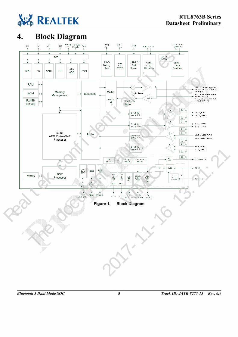
4. Block Diagram
Figure 1. Block Diagram
Realtek confidential files
The document authorized to
WTMEC
2017-11-16 13:21:21
RTL8763B Series
Datasheet Preliminary
Bluetooth 5 Dual Mode SOC 6 Track ID: JATR-8275-15 Rev. 0.9
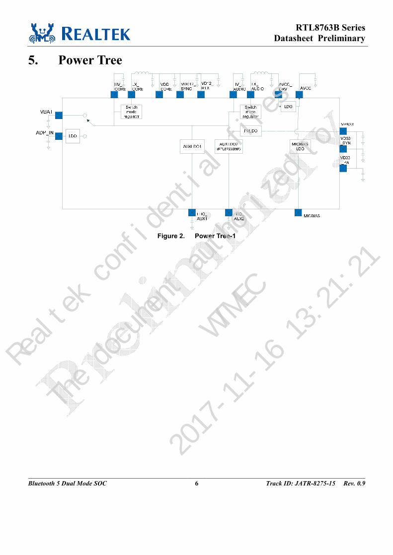
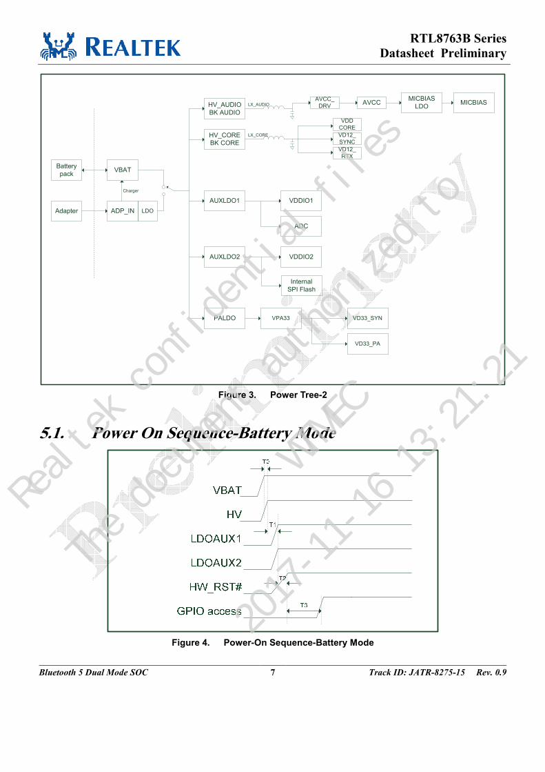
5. Power Tree
Figure 2. Power Tree-1
Realtek confidential files
The document authorized to
WTMEC
2017-11-16 13:21:21
RTL8763B Series
Datasheet Preliminary
Bluetooth 5 Dual Mode SOC 7 Track ID: JATR-8275-15 Rev. 0.9
VBAT
ADP_IN
HV_AUDIO
BK AUDIO
HV_CORE
BK CORE
AUXLDO1
AUXLDO2
PALDO
LX_AUDIO
AVCC_
DRV
LX_CORE
VDD
CORE
VD12_
SYNC
VD12_
RTX
VDDIO1
VDDIO2
VPA33 VD33_SYN
VD33_PA
Charger
Battery
pack
Adapter
AVCC
Internal
SPI Flash
ADC
LDO
MICBIAS
LDOMICBIAS
Figure 3. Power Tree-2
5.1. Power On Sequence-Battery Mode
Figure 4. Power-On Sequence-Battery Mode
Realtek confidential files
The document authorized to
WTMEC
2017-11-16 13:21:21
RTL8763B Series
Datasheet Preliminary
Bluetooth 5 Dual Mode SOC 8 Track ID: JATR-8275-15 Rev. 0.9
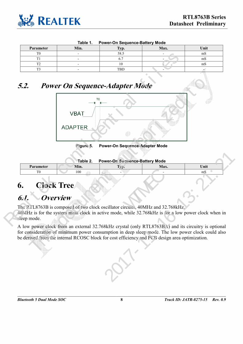
Table 1. Power-On Sequence-Battery Mode
Parameter Min. Typ. Max. Unit
T0 - 58.5 - mS
T1 - 6.7 - mS
T2 - 10 - mS
T3 - TBD - -
5.2. Power On Sequence-Adapter Mode
Figure 5. Power-On Sequence-Adapter Mode
Table 2. Power-On Sequence-Battery Mode
Parameter Min. Typ. Max. Unit
T0 100 - - mS
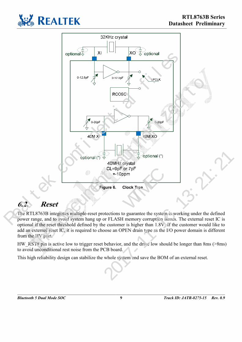
6. Clock Tree
6.1. Overview The RTL8763B is composed of two clock oscillator circuits, 40MHz and 32.768kHz.
40MHz is for the system main clock in active mode, while 32.768kHz is for a low power clock when in
sleep mode.
A low power clock from an external 32.768kHz crystal (only RTL8763BA) and its circuitry is optional
for consideration of minimum power consumption in deep sleep mode. The low power clock could also
be derived from the internal RCOSC block for cost efficiency and PCB design area optimization.
Realtek confidential files
The document authorized to
WTMEC
2017-11-16 13:21:21
RTL8763B Series
Datasheet Preliminary
Bluetooth 5 Dual Mode SOC 9 Track ID: JATR-8275-15 Rev. 0.9
Figure 6. Clock Tree
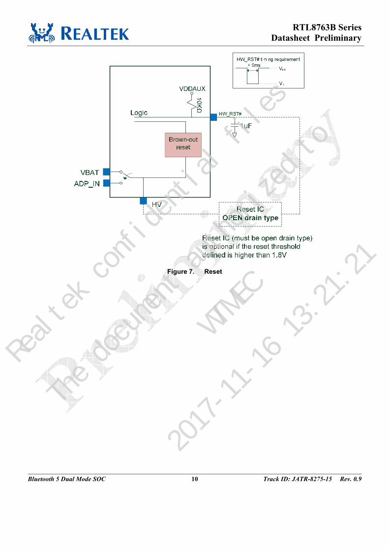
6.2. Reset The RTL8763B integrates multiple-reset protections to guarantee the system is working under the defined
power range, and to avoid system hang up or FLASH memory corruption issues. The external reset IC is
optional if the reset threshold defined by the customer is higher than 1.8V. If the customer would like to
add an external reset IC, it is required to choose an OPEN drain type as the I/O power domain is different
from the HV port.
HW_RST# pin is active low to trigger reset behavior, and the drive low should be longer than 8ms (>8ms)
to avoid unconditional rest noise from the PCB board.
This high reliability design can stabilize the whole system and save the BOM of an external reset.
Realtek confidential files
The document authorized to
WTMEC
2017-11-16 13:21:21
RTL8763B Series
Datasheet Preliminary
Bluetooth 5 Dual Mode SOC 10 Track ID: JATR-8275-15 Rev. 0.9
Figure 7. Reset
Realtek confidential files
The document authorized to
WTMEC
2017-11-16 13:21:21
RTL8763B Series
Datasheet Preliminary
Bluetooth 5 Dual Mode SOC 11 Track ID: JATR-8275-15 Rev. 0.9
7. Pin Assignments
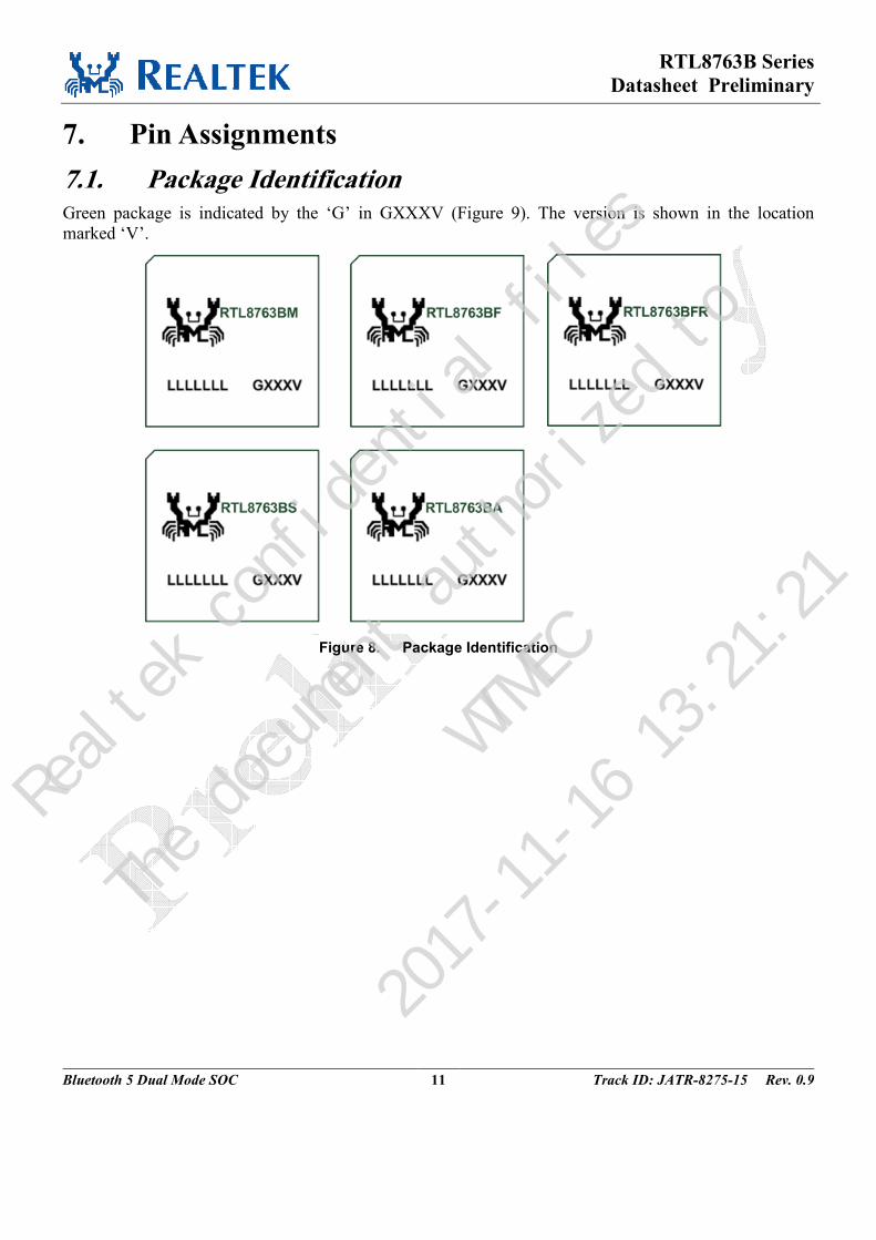
7.1. Package Identification Green package is indicated by the ‘G’ in GXXXV (Figure 9). The version is shown in the location
marked ‘V’.
Figure 8. Package Identification
Realtek confidential files
The document authorized to
WTMEC
2017-11-16 13:21:21
RTL8763B Series
Datasheet Preliminary
Bluetooth 5 Dual Mode SOC 12 Track ID: JATR-8275-15 Rev. 0.9
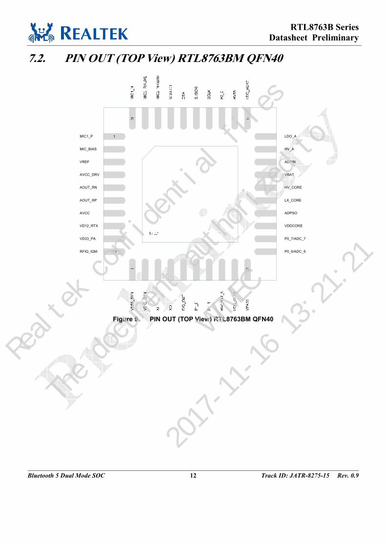
7.2. PIN OUT (TOP View) RTL8763BM QFN40
1
10
MIC1_P
MIC_BIAS
VREF
AVCC_DRV
AOUT_RN
AOUT_RP
AVCC
VD12_RTX
VD33_PA
RFIQ_IQM
LDO_A
HV_A
ADPIN
VBAT
HV_CORE
LX_CORE
ADPSO
VDDCORE
P0_7/ADC_7
P0_6/ADC_6
41: EP
Figure 9. PIN OUT (TOP View) RTL8763BM QFN40
Realtek confidential files
The document authorized to
WTMEC
2017-11-16 13:21:21
RTL8763B Series
Datasheet Preliminary
Bluetooth 5 Dual Mode SOC 13 Track ID: JATR-8275-15 Rev. 0.9
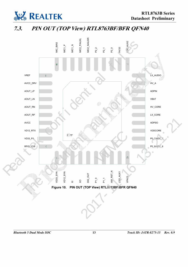
7.3. PIN OUT (TOP View) RTL8763BF/BFR QFN40
1
10
4
0
3
1
1
1
2
0
VREF
AVCC_DRV
AOUT_RN
AOUT_RP
AVCC
VD12_RTX
VD33_PA
RFIQ_IQM
LX_AUDIO
HV_A
ADPIN
VBAT
HV_CORE
LX_CORE
ADPSO
VDDCORE
P0_7/ADC_7
P0_6/ADC_6
MIC
1_
N
MIC
2_
P/A
UX
L
MIC
2_
N/A
UX
R
P2
_2
P2
_1
P2
_0
HV
33
LD
O_A
UX
2
VD
33_
SY
N
VD
12_
SY
N
XI
XO
DIG
_O
UT
P1
_0
P1
_1
HW
_R
ST
_N
LD
O_
AU
X1
VP
A3
3
41: EP
AOUT_LP
AOUT_LN
MIC
1_
P
MIC
_B
IAS
Figure 10. PIN OUT (TOP View) RTL8763BF/BFR QFN40
Realtek confidential files
The document authorized to
WTMEC
2017-11-16 13:21:21
RTL8763B Series
Datasheet Preliminary
Bluetooth 5 Dual Mode SOC 14 Track ID: JATR-8275-15 Rev. 0.9
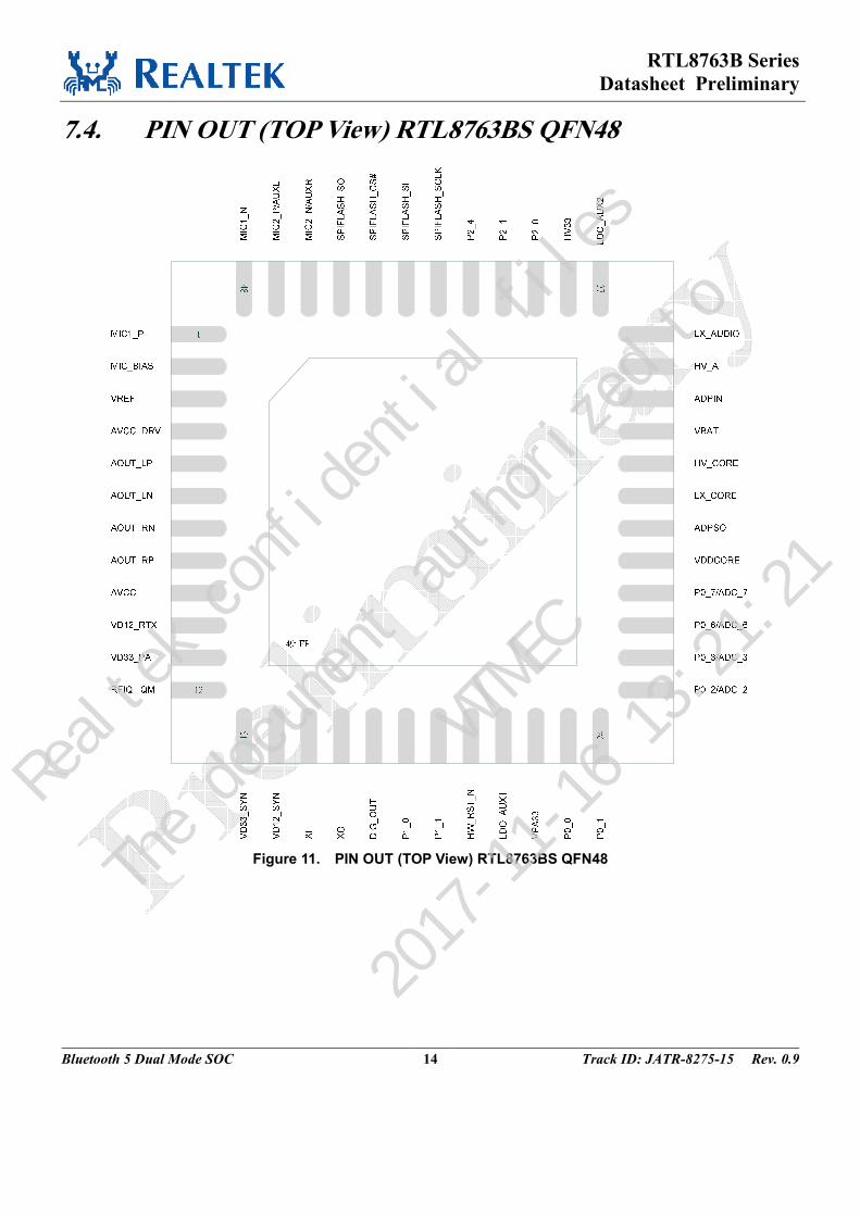
7.4. PIN OUT (TOP View) RTL8763BS QFN48
Figure 11. PIN OUT (TOP View) RTL8763BS QFN48
Realtek confidential files
The document authorized to
WTMEC
2017-11-16 13:21:21
RTL8763B Series
Datasheet Preliminary
Bluetooth 5 Dual Mode SOC 15 Track ID: JATR-8275-15 Rev. 0.9
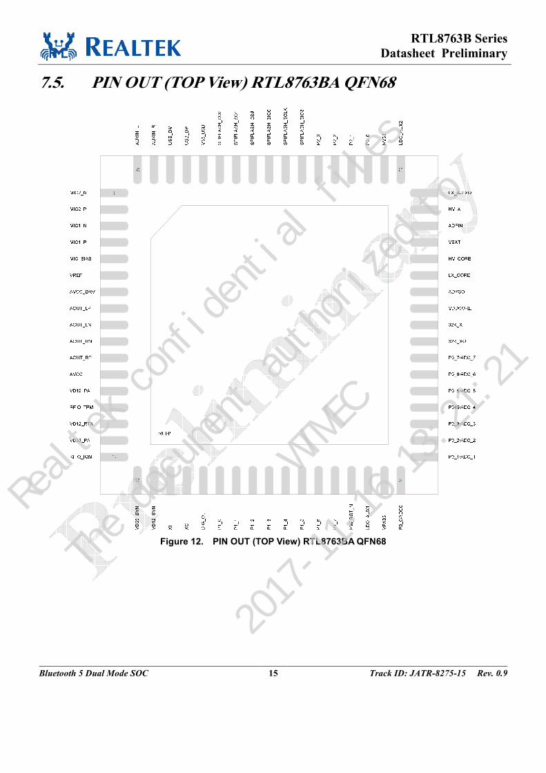
7.5. PIN OUT (TOP View) RTL8763BA QFN68
Figure 12. PIN OUT (TOP View) RTL8763BA QFN68
Realtek confidential files
The document authorized to
WTMEC
2017-11-16 13:21:21
RTL8763B Series
Datasheet Preliminary
Bluetooth 5 Dual Mode SOC 16 Track ID: JATR-8275-15 Rev. 0.9
8. Pin Descriptions
8.1. RF Interface Table 3. RF Interface
Pin Name Pad
Type
RTL
8763BM
RTL
8763BF/
BFR
RTL
8763BS
RTL
8763BA Description
RFIO_IQM RF 10 10 12 17 Bluetooth radio 50Ω transmitter output
and receiver input (dual mode)
RFIO_TPM RF - - - 14 Bluetooth radio 50Ω transmitter output
and receiver input (BLE)
8.2. Crystal Oscillator Table 4. Crystal Oscillator
Pin Name Pad
Type
RTL
8763BM
RTL
8763BF/
BFR
RTL
8763BS
RTL
8763BA Description
XI A 13 13 15 20 Crystal input
XO A 14 14 16 21 Crystal output
A: Analog
8.3. General Purpose I/Os Table 5. General Purpose I/Os
Pin Name Pad
Type
RTL
8763BM
RTL
8763BF/
BFR
RTL
8763BS
RTL
8763BA Description
P0_0/ADC_0 I/O
I/O A - - 23 34
Programmable GPIO. Can be
programmed as ADC input pin
Pull high/low input configurable
P0_1/ADC_1 I/O
I/O A - - 24 35
Programmable GPIO. Can be
programmed as ADC input pin
Pull high/low input configurable
P0_2/ADC_2 I/O
I/O A - - 25 36
Programmable GPIO. Can be
programmed as ADC input pin
Pull high/low input configurable
P0_3/ADC_3 I/O
I/O A - - 26 37
Programmable GPIO. Can be
programmed as ADC input pin
Pull high/low input configurable
P0_4/ADC_4 I/O
I/O A - - - 38
Programmable GPIO. Can be
programmed as ADC input pin
Pull high/low input configurable
Realtek confidential files
The document authorized to
WTMEC
2017-11-16 13:21:21
RTL8763B Series
Datasheet Preliminary
Bluetooth 5 Dual Mode SOC 17 Track ID: JATR-8275-15 Rev. 0.9
Pin Name Pad
Type
RTL
8763BM
RTL
8763BF/
BFR
RTL
8763BS
RTL
8763BA Description
P0_5/ADC_5 I/O I/O
A - - - 39
Programmable GPIO. Can be
programmed as ADC input pin
Pull high/low input configurable
P0_6/ADC_6 I/O I/O
A 21 21 27 40
Programmable GPIO. Can be
programmed as ADC input pin
Pull high/low input configurable
P0_7/ADC_7 I/O I/O
A 22 22 28 41
Programmable GPIO. Can be
programmed as ADC input pin
Pull high/low input configurable
P1_0 I/O 16 16 18 23 Programmable GPI and MFB for power
on
P1_1 I/O 17 17 19 24 Programmable GPIO
Pull high/low input configurable
P1_2 I/O - - - 25 Programmable GPIO
Pull high/low input configurable
P1_3 I/O - - - 26 Programmable GPIO
Pull high/low input configurable
P1_4 I/O - - - 27 Programmable GPIO
Pull high/low input configurable
P1_5 I/O - - - 28 Programmable GPIO
Pull high/low input configurable
P1_6 I/O - - - 29 Programmable GPIO
Pull high/low input configurable
P1_7 I/O - - - 30 Programmable GPIO
Pull high/low input configurable
P2_0 I/O 33 33 39 54 Programmable GPIO
Pull high/low input configurable
P2_1 I/O - 34 40 55 Programmable GPIO
Pull high/low input configurable
P2_2 I/O - 35 - 56 Programmable GPIO
Pull high/low input configurable
P2_3 I/O - - - 57 Programmable GPIO
Pull high/low input configurable
P2_4 I/O - 41 - Programmable GPIO
Pull high/low input configurable
I/O: Bidirectional digital pad
I/O PU: Bidirectional digital pad with pull high resistor inside when input mode
I/O PD: Bidirectional digital pad with pull low resistor inside when input mode
I/O A: Bidirectional digital pad and programmable ADC
Realtek confidential files
The document authorized to
WTMEC
2017-11-16 13:21:21
RTL8763B Series
Datasheet Preliminary
Bluetooth 5 Dual Mode SOC 18 Track ID: JATR-8275-15 Rev. 0.9
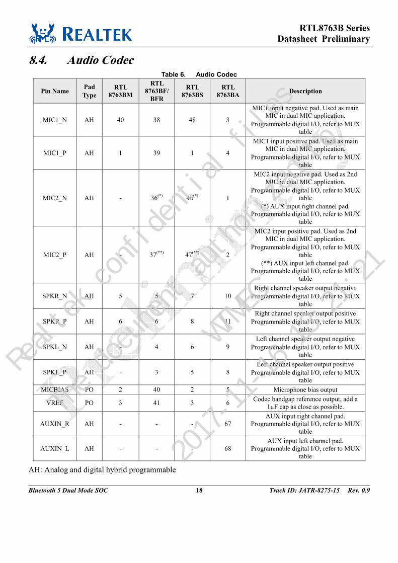
8.4. Audio Codec Table 6. Audio Codec
Pin Name Pad
Type
RTL
8763BM
RTL
8763BF/
BFR
RTL
8763BS
RTL
8763BA Description
MIC1_N AH 40 38 48 3
MIC1 input negative pad. Used as main
MIC in dual MIC application.
Programmable digital I/O, refer to MUX
table
MIC1_P AH 1 39 1 4
MIC1 input positive pad. Used as main
MIC in dual MIC application.
Programmable digital I/O, refer to MUX
table
MIC2_N AH - 36(*)
46(*)
1
MIC2 input negative pad. Used as 2nd
MIC in dual MIC application.
Programmable digital I/O, refer to MUX
table
(*) AUX input right channel pad.
Programmable digital I/O, refer to MUX
table
MIC2_P AH - 37(**)
47(**)
2
MIC2 input positive pad. Used as 2nd
MIC in dual MIC application.
Programmable digital I/O, refer to MUX
table
(**) AUX input left channel pad.
Programmable digital I/O, refer to MUX
table
SPKR_N AH 5 5 7 10
Right channel speaker output negative
Programmable digital I/O, refer to MUX
table
SPKR_P AH 6 6 8 11
Right channel speaker output positive
Programmable digital I/O, refer to MUX
table
SPKL_N AH - 4 6 9
Left channel speaker output negative
Programmable digital I/O, refer to MUX
table
SPKL_P AH - 3 5 8
Left channel speaker output positive
Programmable digital I/O, refer to MUX
table
MICBIAS PO 2 40 2 5 Microphone bias output
VREF PO 3 41 3 6 Codec bandgap reference output, add a
1µF cap as close as possible.
AUXIN_R AH - - - 67
AUX input right channel pad.
Programmable digital I/O, refer to MUX
table
AUXIN_L AH - - - 68
AUX input left channel pad.
Programmable digital I/O, refer to MUX
table
AH: Analog and digital hybrid programmable
Realtek confidential files
The document authorized to
WTMEC
2017-11-16 13:21:21
RTL8763B Series
Datasheet Preliminary
Bluetooth 5 Dual Mode SOC 19 Track ID: JATR-8275-15 Rev. 0.9
PO: Power output
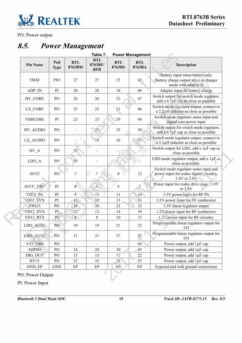
8.5. Power Management Table 7. Power Management
Pin Name Pad
Type
RTL
8763BM
RTL
8763BF/
BFR
RTL
8763BS
RTL
8763BA Description
VBAT PIO 27 27 33 48
Battery input when battery only
Battery charge output when in charger
mode with adapter in
ADP_IN PI 28 28 34 49 Adapter input for battery charge
HV_CORE PO 26 26 32 47 Switch output for switch mode regulator,
add a 4.7µF cap as close as possible
LX_CORE PO 25 25 31 46 Switch mode regulator output, connect to
a 2.2µH inductor as close as possible
VDDCORE PI 23 23 29 44 Switch mode regulator sense input and
digital core power input
HV_AUDIO PO - 29 35 50 Switch output for switch mode regulator,
add a 4.7µF cap as close as possible
LX_AUDIO PO - 30 36 51 Switch mode regulator output, connect to
a 2.2µH inductor as close as possible
HV_A PO 29 - - - Switch output for LDO, add a 1µF cap as
close as possible
LDO_A PO 30 - - - LDO mode regulator output, add a 1µF as
close as possible.
AVCC PO 7 7 9 12
Switch mode regulator sense input and
power input for codec digital circuitry,
1.8V or 2.8V
AVCC_DRV PI 4 4 4 7 Power input for codec drive stage, 1.8V
or 2.8V
VD33_PA PI 9 13 11 16 3.3V power input for RF PA
VD33_SYN PI 11 15 13 18 3.3V power input for RF synthesizer
VPA33 PO 20 20 22 33 3.3V linear regulator output
VD12_SYN PI 12 12 14 19 1.2V power input for RF synthesizer
VD12_RTX PI 8 8 10 15 1.2V power input for RF circuitry
LDO_AUX1 PO 19 19 21 32 Programmable linear regulator output for
I/O
LDO_AUX2 PO 31 31 37 52 Programmable linear regulator output for
I/O
V33_USB PO - - - 64 Power output, add 1µF cap
ADPSO PO 24 24 30 45 Power output, add 1µF cap
DIG_OUT PO 15 15 17 22 Power output, add 1µF cap
HV33 PO 32 32 38 53 Power output, add 1µF cap
GND_EP GND EP EP EP EP Exposed pad with ground connections
PO: Power Output
PI: Power Input
Realtek confidential files
The document authorized to
WTMEC
2017-11-16 13:21:21
RTL8763B Series
Datasheet Preliminary
Bluetooth 5 Dual Mode SOC 20 Track ID: JATR-8275-15 Rev. 0.9
PIO: Power Input and Output
8.6. SPI FLASH Memory Interface Table 8. SPI FLASH Memory Interface
Pin Name Pad
Type
RTL
8763BM
RTL
8763BF/
BFR
RTL
8763BS
RTL
8763BA Description
SPIFLASH_
SCLK O 34 - 42 59
Serial flash clock output
SPIFLASH_
CS# I/O 36 - 44 61
Serial flash chip select, low active
SPIFLASH_SI/
SIO0 I/O 35 - 43 60
Serial flash data output for 1-bit mode,
connect to SI pin of external FLASH
memory
Serial flash data output for 4-bit mode,
connect to SIO0 pin of external FLASH
memory
SPIFLASH_SO/
SIO1 I/O 37 - 45 62
Serial flash data input for 1-bit mode,
connect to SO pin of external FLASH
memory
Serial flash data output for 4-bit mode,
connect to SIO1 pin of external FLASH
memory
SPIFLASH_
WP#/SIO2 I/O - - - 63
Serial flash data output for 4-bit mode,
connect to SIO2 pin of external FLASH
memory
SPIFLASH_
HOLD#/SIO3 I/O - - - 58
Serial flash data output for 4-bit mode,
connect to SIO3 pin of external FLASH
memory
O: Digital output
I: Digital input
8.7. System Table 9. System
Pin Name Pad
Type
RTL
8763BM
RTL
8763BF/
BFR
RTL
8763BS
RTL
8763BA Description
HW_RST# I_PU 18 18 20 31
System reset input with internal pull high,
low active with at least 5ms low to trigger
system reset
USB_DP AI/O - - - 65 USB signal positive
USB_DN AI/O - - - 66 USB signal negative
I_PU: Input with internal pull high inside
Realtek confidential files
The document authorized to
WTMEC
2017-11-16 13:21:21
RTL8763B Series
Datasheet Preliminary
Bluetooth 5 Dual Mode SOC 21 Track ID: JATR-8275-15 Rev. 0.9
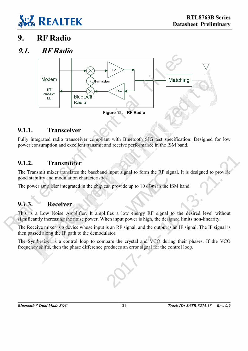
9. RF Radio
9.1. RF Radio
Figure 13. RF Radio
9.1.1. Transceiver
Fully integrated radio transceiver compliant with Bluetooth SIG test specification. Designed for low
power consumption and excellent transmit and receive performance in the ISM band.
9.1.2. Transmitter
The Transmit mixer translates the baseband input signal to form the RF signal. It is designed to provide
good stability and modulation characteristics.
The power amplifier integrated in the chip can provide up to 10 dBm in the ISM band.
9.1.3. Receiver
This is a Low Noise Amplifier. It amplifies a low energy RF signal to the desired level without
significantly increasing the noise power. When input power is high, the designed limits non-linearity.
The Receive mixer is a device whose input is an RF signal, and the output is an IF signal. The IF signal is
then passed along the IF path to the demodulator.
The Synthesizer is a control loop to compare the crystal and VCO during their phases. If the VCO
frequency shifts, then the phase difference produces an error signal for the control loop.
Realtek confidential files
The document authorized to
WTMEC
2017-11-16 13:21:21
RTL8763B Series
Datasheet Preliminary
Bluetooth 5 Dual Mode SOC 22 Track ID: JATR-8275-15 Rev. 0.9
9.1.4. RF IQM and TPM
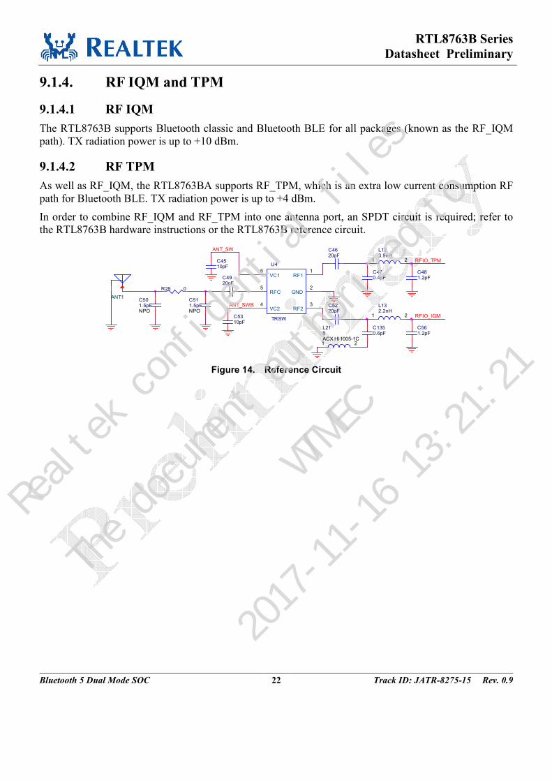
9.1.4.1 RF IQM
The RTL8763B supports Bluetooth classic and Bluetooth BLE for all packages (known as the RF_IQM
path). TX radiation power is up to +10 dBm.
9.1.4.2 RF TPM
As well as RF_IQM, the RTL8763BA supports RF_TPM, which is an extra low current consumption RF
path for Bluetooth BLE. TX radiation power is up to +4 dBm.
In order to combine RF_IQM and RF_TPM into one antenna port, an SPDT circuit is required; refer to
the RTL8763B hardware instructions or the RTL8763B reference circuit.
Figure 14. Reference Circuit
C1350.6pF
L210ACX HI1005-1C1 2
ANT_SW
RFIO_IQM
RFIO_TPM
ANT_SWB L132.2nH
1 2
C470.4pFC49
20pF
C561.2pF
ANT1
C5220pF
C481.2pF
C511.5pFNPO
L123.9nH
1 2
C4620pF
U4
TRSW
RF11
GND2
RF23
VC24
RFC5
VC16
C5310pF
C501.5pFNPO
C4510pF
R25 0
Realtek confidential files
The document authorized to
WTMEC
2017-11-16 13:21:21
RTL8763B Series
Datasheet Preliminary
Bluetooth 5 Dual Mode SOC 23 Track ID: JATR-8275-15 Rev. 0.9
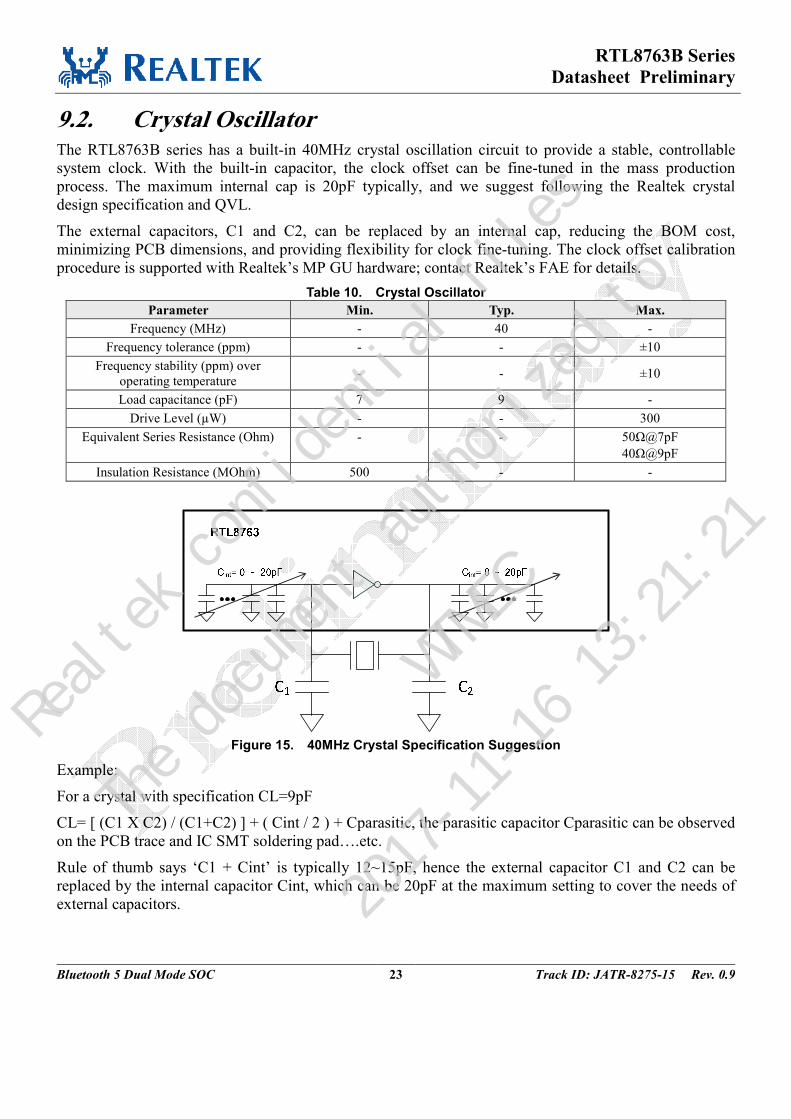
9.2. Crystal Oscillator The RTL8763B series has a built-in 40MHz crystal oscillation circuit to provide a stable, controllable
system clock. With the built-in capacitor, the clock offset can be fine-tuned in the mass production
process. The maximum internal cap is 20pF typically, and we suggest following the Realtek crystal
design specification and QVL.
The external capacitors, C1 and C2, can be replaced by an internal cap, reducing the BOM cost,
minimizing PCB dimensions, and providing flexibility for clock fine-tuning. The clock offset calibration
procedure is supported with Realtek’s MP GU hardware; contact Realtek’s FAE for details.
Table 10. Crystal Oscillator
Parameter Min. Typ. Max.
Frequency (MHz) - 40 -
Frequency tolerance (ppm) - - ±10
Frequency stability (ppm) over
operating temperature - - ±10
Load capacitance (pF) 7 9 -
Drive Level (µW) - - 300
Equivalent Series Resistance (Ohm) - - 50Ω@7pF
40Ω@9pF
Insulation Resistance (MOhm) 500 - -
Figure 15. 40MHz Crystal Specification Suggestion
Example:
For a crystal with specification CL=9pF
CL= [ (C1 X C2) / (C1+C2) ] + ( Cint / 2 ) + Cparasitic, the parasitic capacitor Cparasitic can be observed
on the PCB trace and IC SMT soldering pad….etc.
Rule of thumb says ‘C1 + Cint’ is typically 12~15pF, hence the external capacitor C1 and C2 can be
replaced by the internal capacitor Cint, which can be 20pF at the maximum setting to cover the needs of
external capacitors.
Realtek confidential files
The document authorized to
WTMEC
2017-11-16 13:21:21
RTL8763B Series
Datasheet Preliminary
Bluetooth 5 Dual Mode SOC 24 Track ID: JATR-8275-15 Rev. 0.9
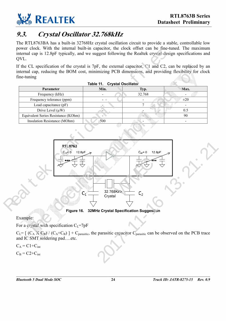
9.3. Crystal Oscillator 32.768kHz The RTL8763BA has a built-in 32768Hz crystal oscillation circuit to provide a stable, controllable low
power clock. With the internal built-in capacitor, the clock offset can be fine-tuned. The maximum
internal cap is 12.8pF typically, and we suggest following the Realtek crystal design specifications and
QVL.
If the CL specification of the crystal is 7pF, the external capacitor, C1 and C2, can be replaced by an
internal cap, reducing the BOM cost, minimizing PCB dimensions, and providing flexibility for clock
fine-tuning
Table 11. Crystal Oscillator
Parameter Min. Typ. Max.
Frequency (kHz) - 32.768 -
Frequency tolerance (ppm) - - ±20
Load capacitance (pF) - 7 -
Drive Level (µW) - - 0.5
Equivalent Series Resistance (KOhm) - - 90
Insulation Resistance (MOhm) 500 - -
Figure 16. 32MHz Crystal Specification Suggestion
Example:
For a crystal with specification CL=7pF
CL= [ (CA X CB) / (CA+CB) ] + Cparasitic, the parasitic capacitor Cparasitic can be observed on the PCB trace
and IC SMT soldering pad….etc.
CA = C1+Cint
CB = C2+Cint
Realtek confidential files
The document authorized to
WTMEC
2017-11-16 13:21:21
RTL8763B Series
Datasheet Preliminary
Bluetooth 5 Dual Mode SOC 25 Track ID: JATR-8275-15 Rev. 0.9
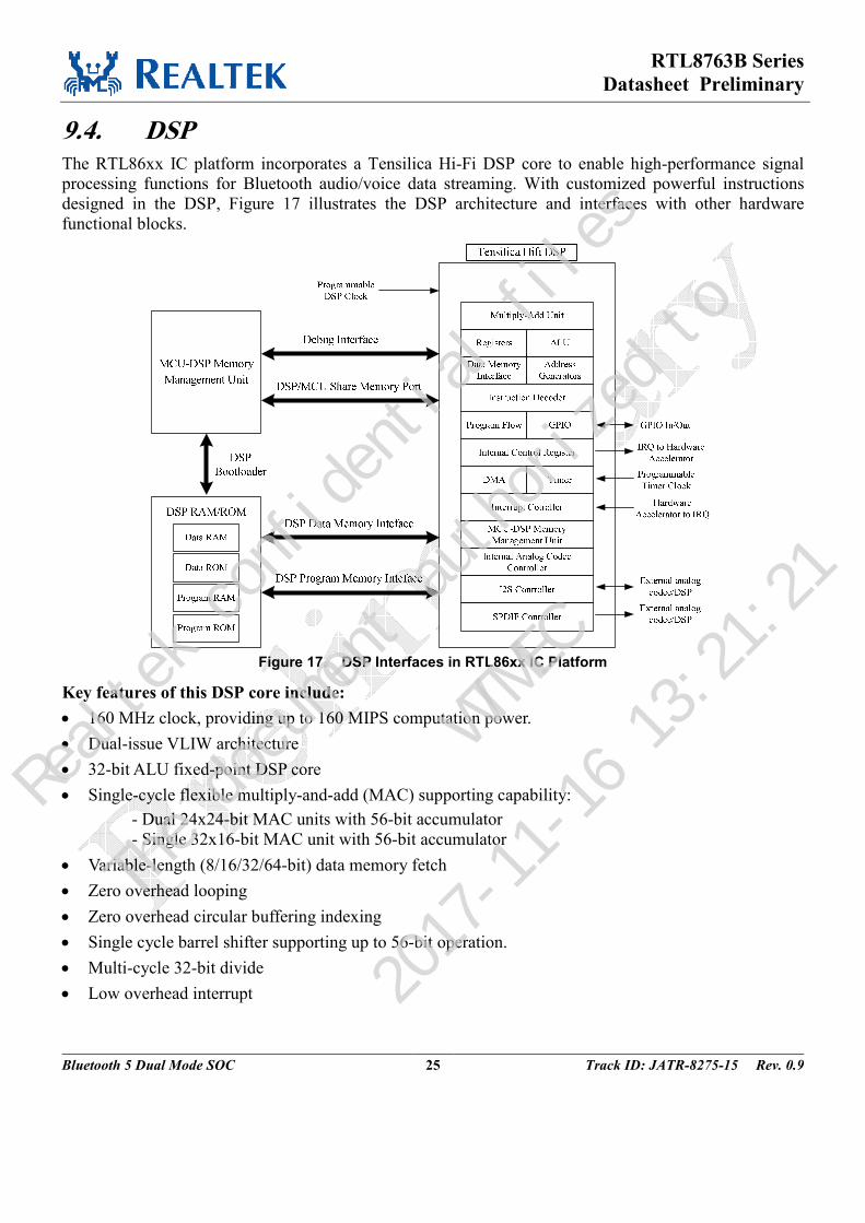
9.4. DSP The RTL86xx IC platform incorporates a Tensilica Hi-Fi DSP core to enable high-performance signal
processing functions for Bluetooth audio/voice data streaming. With customized powerful instructions
designed in the DSP, Figure 17 illustrates the DSP architecture and interfaces with other hardware
functional blocks.
Figure 17. DSP Interfaces in RTL86xx IC Platform
Key features of this DSP core include:
• 160 MHz clock, providing up to 160 MIPS computation power.
• Dual-issue VLIW architecture
• 32-bit ALU fixed-point DSP core
• Single-cycle flexible multiply-and-add (MAC) supporting capability:
- Dual 24x24-bit MAC units with 56-bit accumulator
- Single 32x16-bit MAC unit with 56-bit accumulator
• Variable-length (8/16/32/64-bit) data memory fetch
• Zero overhead looping
• Zero overhead circular buffering indexing
• Single cycle barrel shifter supporting up to 56-bit operation.
• Multi-cycle 32-bit divide
• Low overhead interrupt
Realtek confidential files
The document authorized to
WTMEC
2017-11-16 13:21:21
RTL8763B Series
Datasheet Preliminary
Bluetooth 5 Dual Mode SOC 26 Track ID: JATR-8275-15 Rev. 0.9
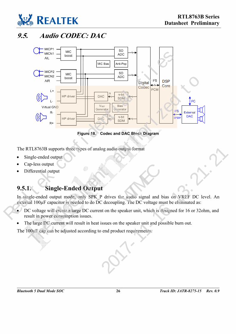
9.5. Audio CODEC: DAC
Figure 18. Codec and DAC Block Diagram
The RTL8763B supports three types of analog audio output format
• Single-ended output
• Cap-less output
• Differential output
9.5.1. Single-Ended Output
In single-ended output mode, only SPK_P drives the audio signal and bias on VREF DC level. An
external 100µF capacitor is needed to do DC decoupling. The DC voltage must be eliminated as:
• DC voltage will create a large DC current on the speaker unit, which is designed for 16 or 32ohm, and
result in power consumption issues.
• The large DC current will result in heat issues on the speaker unit and possible burn out.
The 100µF cap can be adjusted according to end product requirements.
Realtek confidential files
The document authorized to
WTMEC
2017-11-16 13:21:21
RTL8763B Series
Datasheet Preliminary
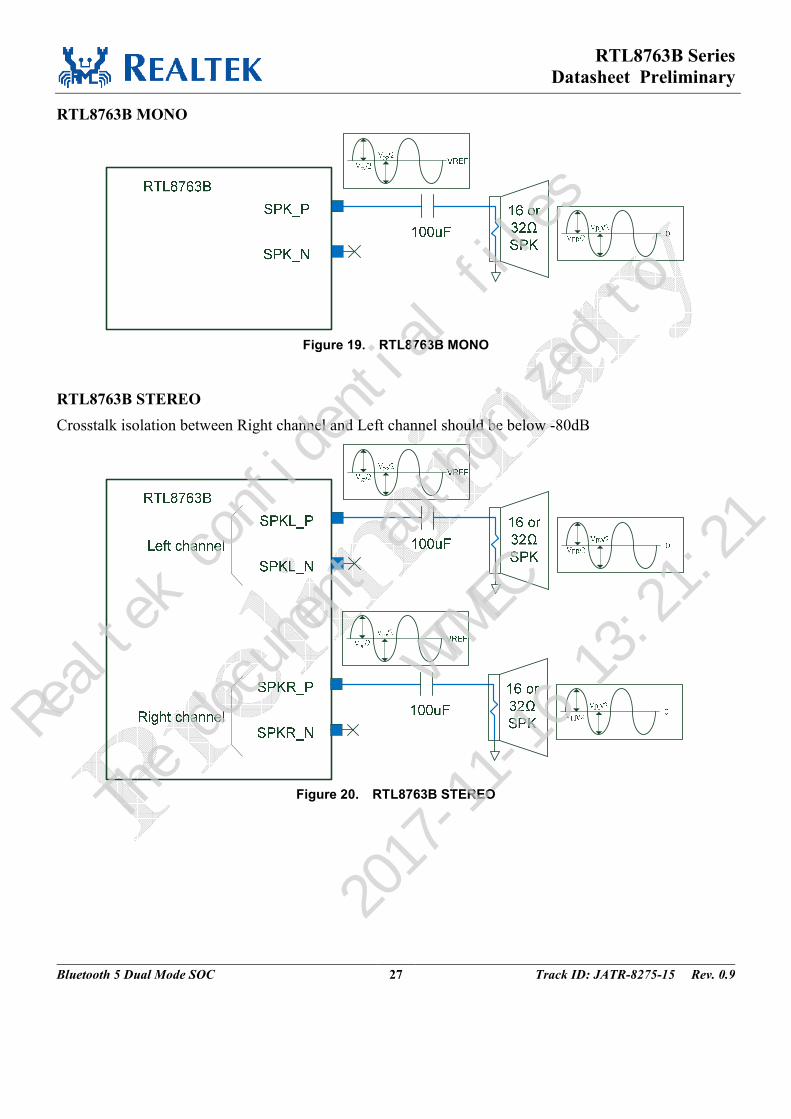
Bluetooth 5 Dual Mode SOC 27 Track ID: JATR-8275-15 Rev. 0.9
RTL8763B MONO
Figure 19. RTL8763B MONO
RTL8763B STEREO
Crosstalk isolation between Right channel and Left channel should be below -80dB
Figure 20. RTL8763B STEREO
Realtek confidential files
The document authorized to
WTMEC
2017-11-16 13:21:21
RTL8763B Series
Datasheet Preliminary
Bluetooth 5 Dual Mode SOC 28 Track ID: JATR-8275-15 Rev. 0.9
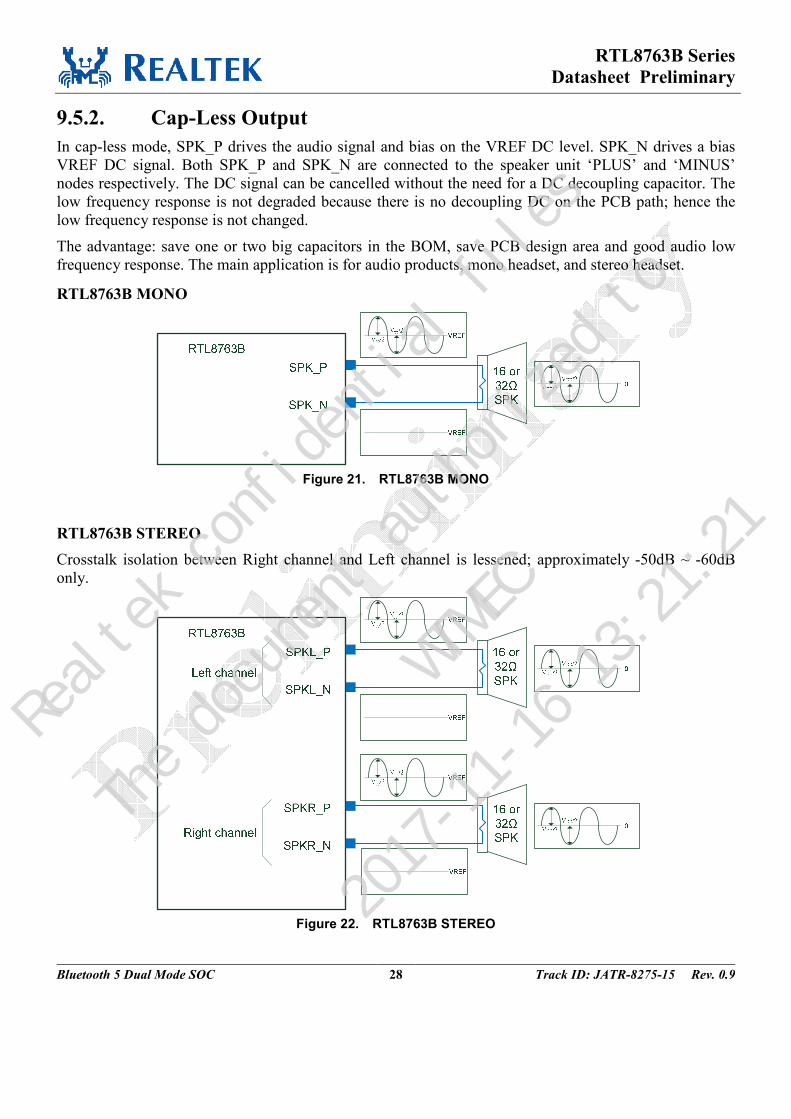
9.5.2. Cap-Less Output
In cap-less mode, SPK_P drives the audio signal and bias on the VREF DC level. SPK_N drives a bias
VREF DC signal. Both SPK_P and SPK_N are connected to the speaker unit ‘PLUS’ and ‘MINUS’
nodes respectively. The DC signal can be cancelled without the need for a DC decoupling capacitor. The
low frequency response is not degraded because there is no decoupling DC on the PCB path; hence the
low frequency response is not changed.
The advantage: save one or two big capacitors in the BOM, save PCB design area and good audio low
frequency response. The main application is for audio products, mono headset, and stereo headset.
RTL8763B MONO
Figure 21. RTL8763B MONO
RTL8763B STEREO
Crosstalk isolation between Right channel and Left channel is lessened; approximately -50dB ~ -60dB
only.
Figure 22. RTL8763B STEREO
Realtek confidential files
The document authorized to
WTMEC
2017-11-16 13:21:21
RTL8763B Series
Datasheet Preliminary
Bluetooth 5 Dual Mode SOC 29 Track ID: JATR-8275-15 Rev. 0.9
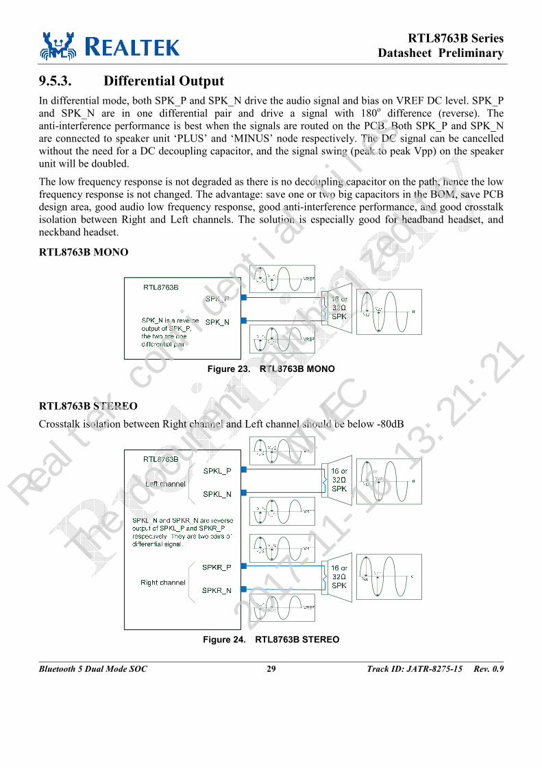
9.5.3. Differential Output
In differential mode, both SPK_P and SPK_N drive the audio signal and bias on VREF DC level. SPK_P
and SPK_N are in one differential pair and drive a signal with 180o difference (reverse). The
anti-interference performance is best when the signals are routed on the PCB. Both SPK_P and SPK_N
are connected to speaker unit ‘PLUS’ and ‘MINUS’ node respectively. The DC signal can be cancelled
without the need for a DC decoupling capacitor, and the signal swing (peak to peak Vpp) on the speaker
unit will be doubled.
The low frequency response is not degraded as there is no decoupling capacitor on the path, hence the low
frequency response is not changed. The advantage: save one or two big capacitors in the BOM, save PCB
design area, good audio low frequency response, good anti-interference performance, and good crosstalk
isolation between Right and Left channels. The solution is especially good for headband headset, and
neckband headset.
RTL8763B MONO
Figure 23. RTL8763B MONO
RTL8763B STEREO
Crosstalk isolation between Right channel and Left channel should be below -80dB
Figure 24. RTL8763B STEREO
Realtek confidential files
The document authorized to
WTMEC
2017-11-16 13:21:21
RTL8763B Series
Datasheet Preliminary
Bluetooth 5 Dual Mode SOC 30 Track ID: JATR-8275-15 Rev. 0.9
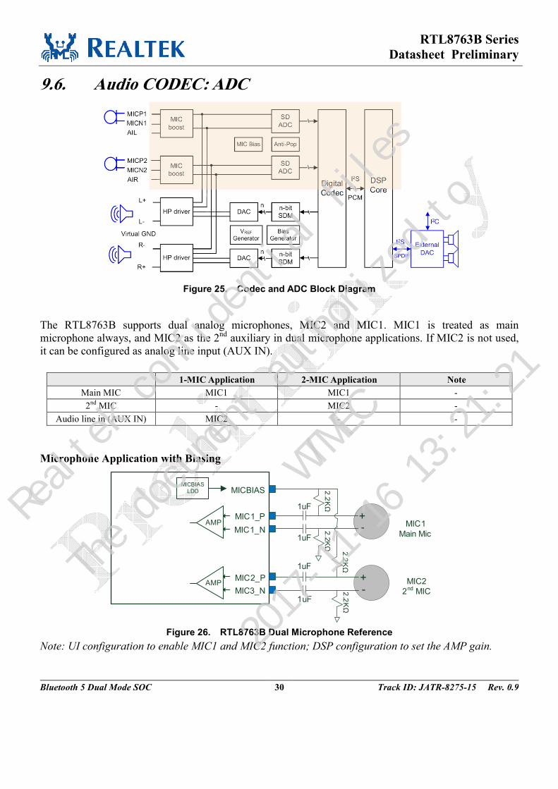
9.6. Audio CODEC: ADC
Figure 25. Codec and ADC Block Diagram
The RTL8763B supports dual analog microphones, MIC2 and MIC1. MIC1 is treated as main
microphone always, and MIC2 as the 2nd
auxiliary in dual microphone applications. If MIC2 is not used,
it can be configured as analog line input (AUX IN).
1-MIC Application 2-MIC Application Note
Main MIC MIC1 MIC1 -
2nd
MIC - MIC2 -
Audio line in (AUX IN) MIC2 - -
Microphone Application with Biasing
MICBIAS
MIC1_P
MIC1_N
MIC2_P
MIC3_N
2.2
KΩ1uF
1uF
+-
1uF
1uF
2.2
KΩ
AMP
AMP
MICBIAS
LDO
MIC1
Main Mic
MIC2
2nd MIC
+-2
.2K
Ω
2.2
KΩ
Figure 26. RTL8763B Dual Microphone Reference
Note: UI configuration to enable MIC1 and MIC2 function; DSP configuration to set the AMP gain.
Realtek confidential files
The document authorized to
WTMEC
2017-11-16 13:21:21
RTL8763B Series
Datasheet Preliminary
Bluetooth 5 Dual Mode SOC 31 Track ID: JATR-8275-15 Rev. 0.9
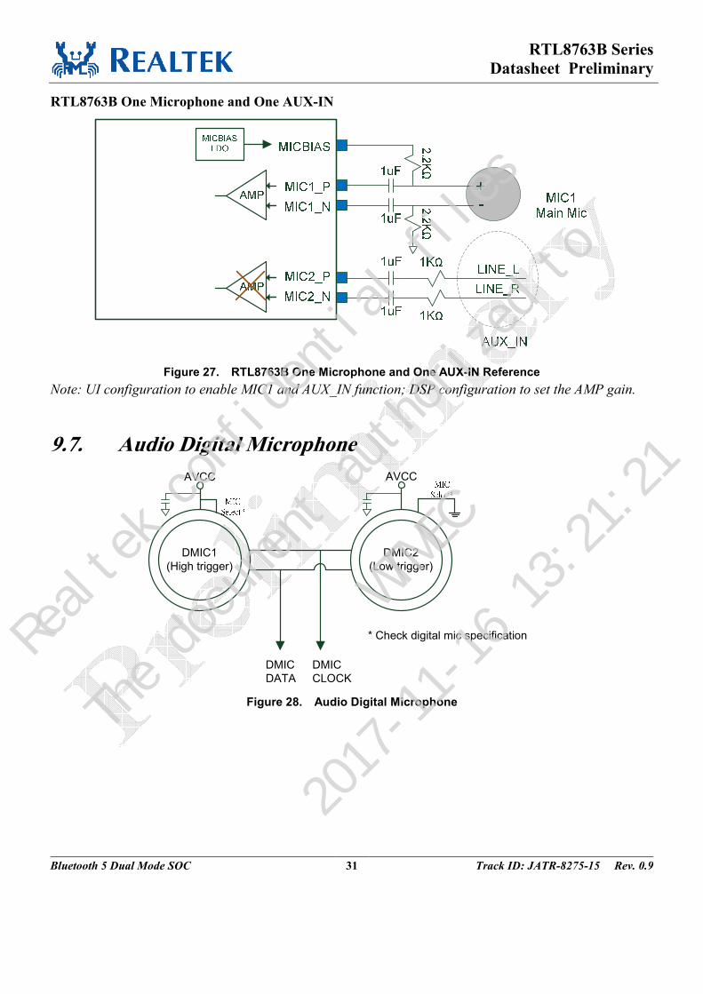
RTL8763B One Microphone and One AUX-IN
Figure 27. RTL8763B One Microphone and One AUX-IN Reference
Note: UI configuration to enable MIC1 and AUX_IN function; DSP configuration to set the AMP gain.
9.7. Audio Digital Microphone
DMIC1
(High trigger)
DMIC2
(Low trigger)
DMIC
DATA
DMIC
CLOCK
AVCC
MIC
Select*
AVCCMIC
Select*
* Check digital mic specification
Figure 28. Audio Digital Microphone
Realtek confidential files
The document authorized to
WTMEC
2017-11-16 13:21:21
RTL8763B Series
Datasheet Preliminary
Bluetooth 5 Dual Mode SOC 32 Track ID: JATR-8275-15 Rev. 0.9
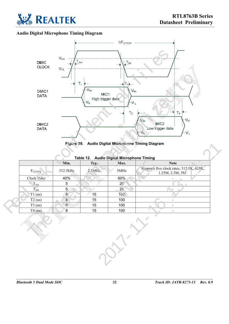
Audio Digital Microphone Timing Diagram
Figure 29. Audio Digital Microphone Timing Diagram
Table 12. Audio Digital Microphone Timing
Min. Typ. Max. Note
FCLOCK 312.5kHz 2.5MHz 5MHz Supports five clock rates, 312.5K, 625K,
1.25M, 2.5M, 5M`
Clock Duty 40% 60% -
Trise 5 20
Tfall 5 20 -
T1 (ns) 8 15 100 -
T2 (ns) 8 15 100 -
T3 (ns) 8 15 100 -
T4 (ns) 8 15 100 -
Realtek confidential files
The document authorized to
WTMEC
2017-11-16 13:21:21
RTL8763B Series
Datasheet Preliminary
Bluetooth 5 Dual Mode SOC 33 Track ID: JATR-8275-15 Rev. 0.9
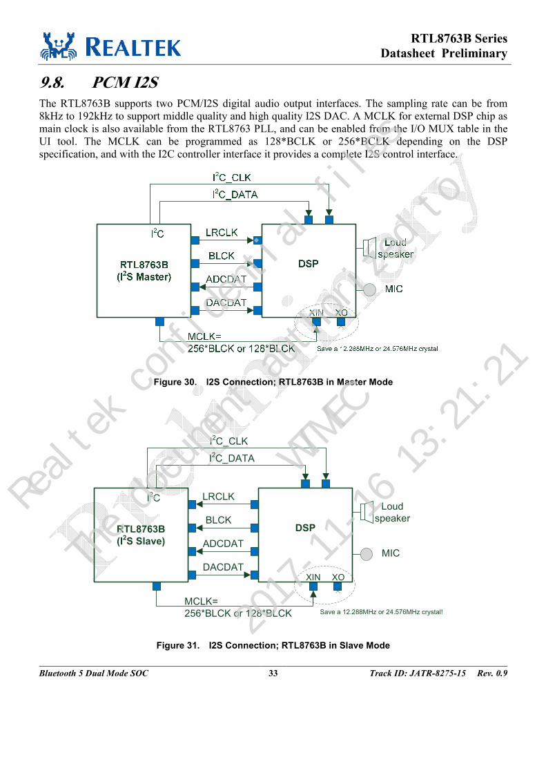
9.8. PCM I2S The RTL8763B supports two PCM/I2S digital audio output interfaces. The sampling rate can be from
8kHz to 192kHz to support middle quality and high quality I2S DAC. A MCLK for external DSP chip as
main clock is also available from the RTL8763 PLL, and can be enabled from the I/O MUX table in the
UI tool. The MCLK can be programmed as 128*BCLK or 256*BCLK depending on the DSP
specification, and with the I2C controller interface it provides a complete I2S control interface.
Figure 30. I2S Connection; RTL8763B in Master Mode
LRCLK
BLCK
ADCDAT
DACDAT
DSP
I2C_DATA
Loud
speaker
MIC
RTL8763B
(I2S Slave)
MCLK=
256*BLCK or 128*BLCK
XIN XO
I2C_CLK
Save a 12.288MHz or 24.576MHz crystal!
I2C
Figure 31. I2S Connection; RTL8763B in Slave Mode
Realtek confidential files
The document authorized to
WTMEC
2017-11-16 13:21:21
RTL8763B Series
Datasheet Preliminary
Bluetooth 5 Dual Mode SOC 34 Track ID: JATR-8275-15 Rev. 0.9
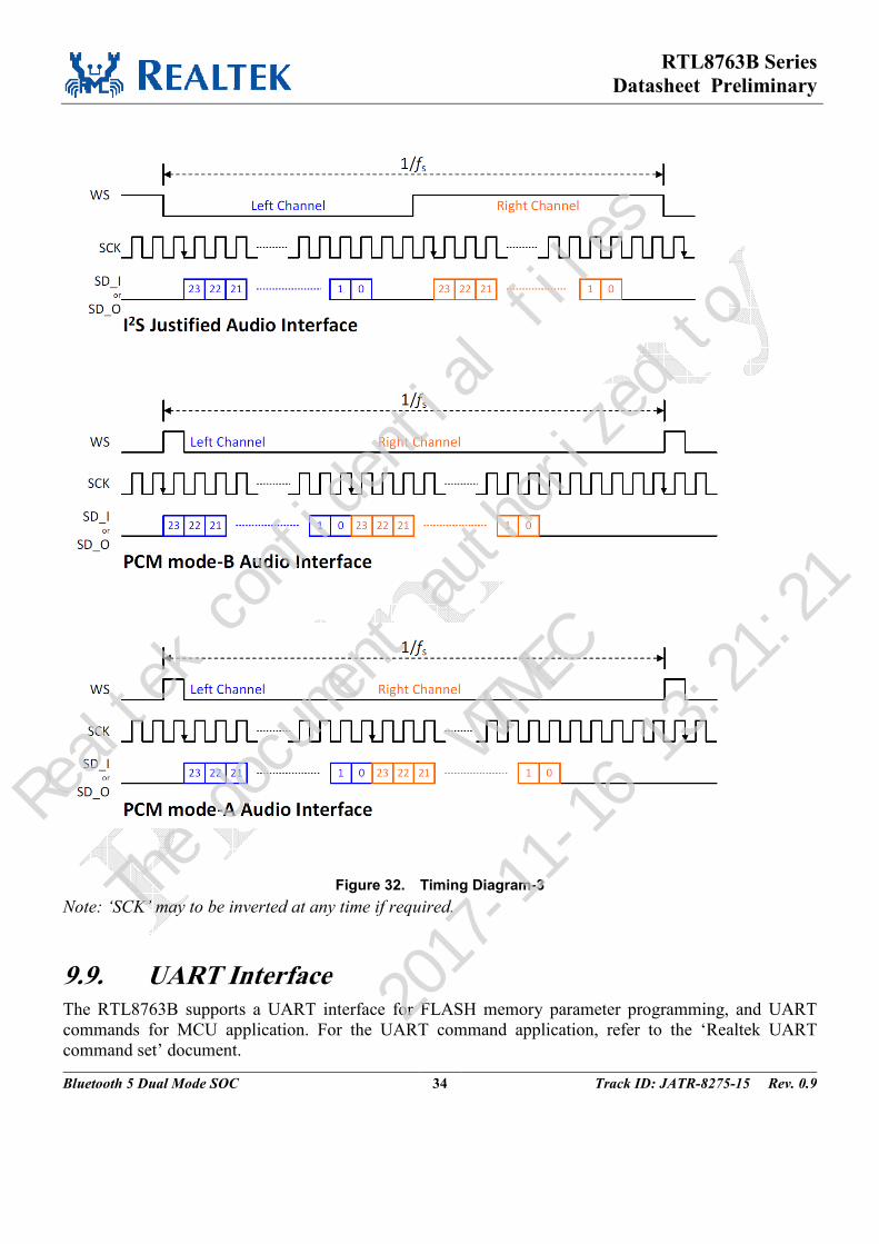
Figure 32. Timing Diagram-3
Note: ‘SCK’ may to be inverted at any time if required.
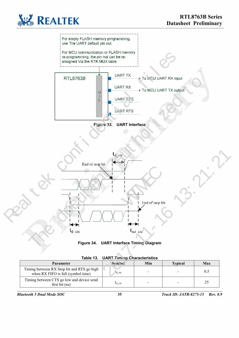
9.9. UART Interface The RTL8763B supports a UART interface for FLASH memory parameter programming, and UART
commands for MCU application. For the UART command application, refer to the ‘Realtek UART
command set’ document.
Realtek confidential files
The document authorized to
WTMEC
2017-11-16 13:21:21
RTL8763B Series
Datasheet Preliminary
Bluetooth 5 Dual Mode SOC 35 Track ID: JATR-8275-15 Rev. 0.9
Figure 33. UART Interface
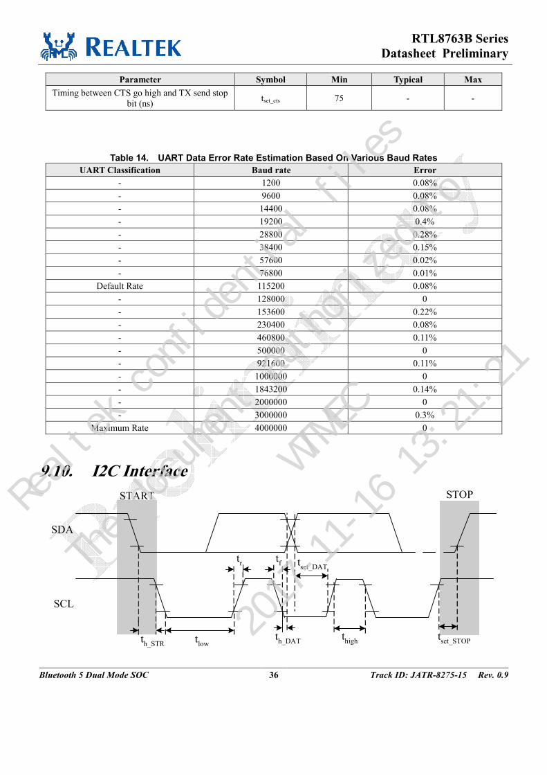
Figure 34. UART Interface Timing Diagram
Table 13. UART Timing Characteristics
Parameter Symbol Min Typical Max
Timing between RX Stop bit and RTS go high
when RX FIFO is full (symbol time) td_rts - - 0.5
Timing between CTS go low and device send
first bit (ns) td_cts - - 25
Realtek confidential files
The document authorized to
WTMEC
2017-11-16 13:21:21
RTL8763B Series
Datasheet Preliminary
Bluetooth 5 Dual Mode SOC 36 Track ID: JATR-8275-15 Rev. 0.9
Parameter Symbol Min Typical Max
Timing between CTS go high and TX send stop
bit (ns) tset_cts 75 - -
Table 14. UART Data Error Rate Estimation Based On Various Baud Rates
UART Classification Baud rate Error
- 1200 0.08%
- 9600 0.08%
- 14400 0.08%
- 19200 0.4%
- 28800 0.28%
- 38400 0.15%
- 57600 0.02%
- 76800 0.01%
Default Rate 115200 0.08%
- 128000 0
- 153600 0.22%
- 230400 0.08%
- 460800 0.11%
- 500000 0
- 921600 0.11%
- 1000000 0
- 1843200 0.14%
- 2000000 0
- 3000000 0.3%
Maximum Rate 4000000 0
9.10. I2C Interface
th_STR
tr
th_DAT
thigh
tf t
set_DAT
tlow
tset_STOP
SCL
SDA
START STOP
Realtek confidential files
The document authorized to
WTMEC
2017-11-16 13:21:21
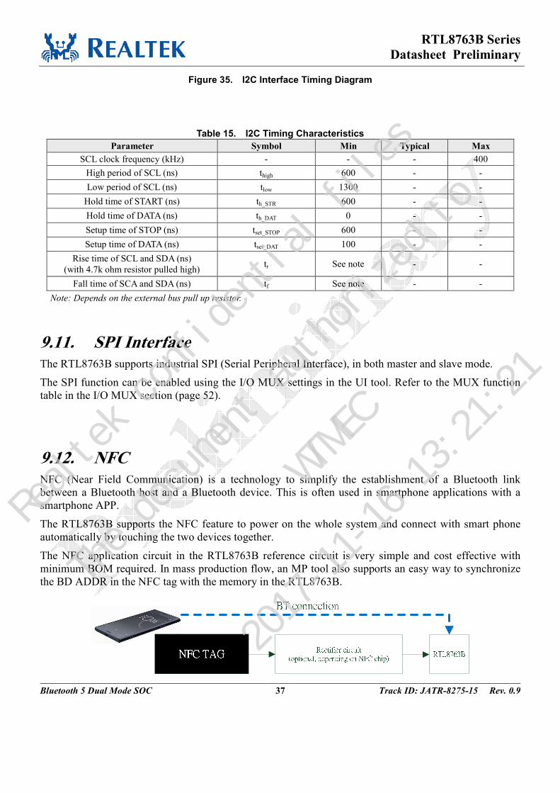
RTL8763B Series
Datasheet Preliminary
Bluetooth 5 Dual Mode SOC 37 Track ID: JATR-8275-15 Rev. 0.9
Figure 35. I2C Interface Timing Diagram
Table 15. I2C Timing Characteristics
Parameter Symbol Min Typical Max
SCL clock frequency (kHz) - - - 400
High period of SCL (ns) thigh 600 - -
Low period of SCL (ns) tlow 1300 - -
Hold time of START (ns) th_STR 600 - -
Hold time of DATA (ns) th_DAT 0 - -
Setup time of STOP (ns) tset_STOP 600 - -
Setup time of DATA (ns) tset_DAT 100 - -
Rise time of SCL and SDA (ns)
(with 4.7k ohm resistor pulled high) tr See note - -
Fall time of SCA and SDA (ns) tf See note - -
Note: Depends on the external bus pull up resistor.
9.11. SPI Interface The RTL8763B supports industrial SPI (Serial Peripheral Interface), in both master and slave mode.
The SPI function can be enabled using the I/O MUX settings in the UI tool. Refer to the MUX function
table in the I/O MUX section (page 52).
9.12. NFC NFC (Near Field Communication) is a technology to simplify the establishment of a Bluetooth link
between a Bluetooth host and a Bluetooth device. This is often used in smartphone applications with a
smartphone APP.
The RTL8763B supports the NFC feature to power on the whole system and connect with smart phone
automatically by touching the two devices together.
The NFC application circuit in the RTL8763B reference circuit is very simple and cost effective with
minimum BOM required. In mass production flow, an MP tool also supports an easy way to synchronize
the BD ADDR in the NFC tag with the memory in the RTL8763B.
Realtek confidential files
The document authorized to
WTMEC
2017-11-16 13:21:21
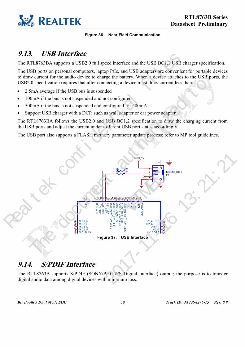
RTL8763B Series
Datasheet Preliminary
Bluetooth 5 Dual Mode SOC 38 Track ID: JATR-8275-15 Rev. 0.9
Figure 36. Near Field Communication
9.13. USB Interface The RTL8763BA supports a USB2.0 full speed interface and the USB BC1.2 USB charger specification.
The USB ports on personal computers, laptop PCs, and USB adapters are convenient for portable devices
to draw current for the audio device to charge the battery. When a device attaches to the USB ports, the
USB2.0 specification requires that after connecting a device must draw current less than:
• 2.5mA average if the USB bus is suspended
• 100mA if the bus is not suspended and not configured
• 500mA if the bus is not suspended and configured for 500mA
• Support USB charger with a DCP, such as wall adapter or car power adapter
The RTL8763BA follows the USB2.0 and USB BC1.2 specification to draw the charging current from
the USB ports and adjust the current under different USB port states accordingly.
The USB port also supports a FLASH memory parameter update process; refer to MP tool guidelines.
Figure 37. USB Interface
9.14. S/PDIF Interface The RTL8763B supports S/PDIF (SONY/PHILIPS Digital Interface) output; the purpose is to transfer
digital audio data among digital devices with minimum loss.
Realtek confidential files
The document authorized to
WTMEC
2017-11-16 13:21:21
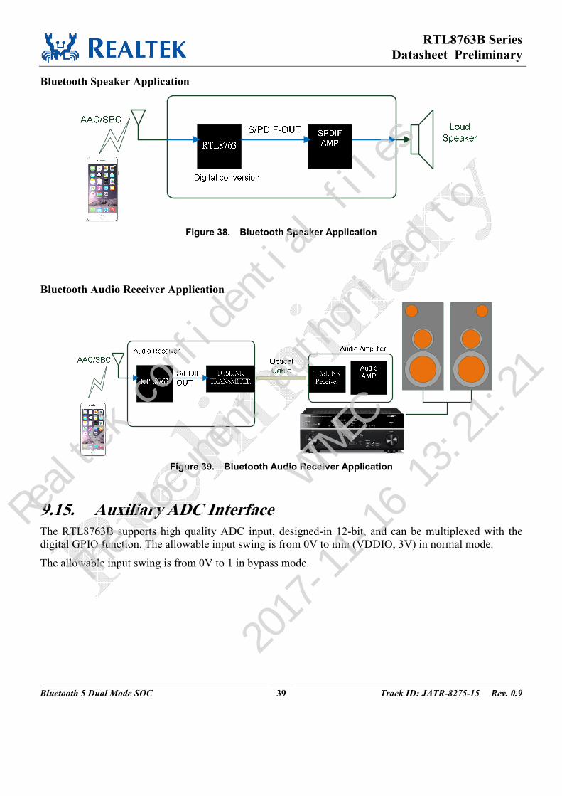
RTL8763B Series
Datasheet Preliminary
Bluetooth 5 Dual Mode SOC 39 Track ID: JATR-8275-15 Rev. 0.9
Bluetooth Speaker Application
Figure 38. Bluetooth Speaker Application
Bluetooth Audio Receiver Application
Figure 39. Bluetooth Audio Receiver Application
9.15. Auxiliary ADC Interface The RTL8763B supports high quality ADC input, designed-in 12-bit, and can be multiplexed with the
digital GPIO function. The allowable input swing is from 0V to min (VDDIO, 3V) in normal mode.
The allowable input swing is from 0V to 1 in bypass mode.
Realtek confidential files
The document authorized to
WTMEC
2017-11-16 13:21:21
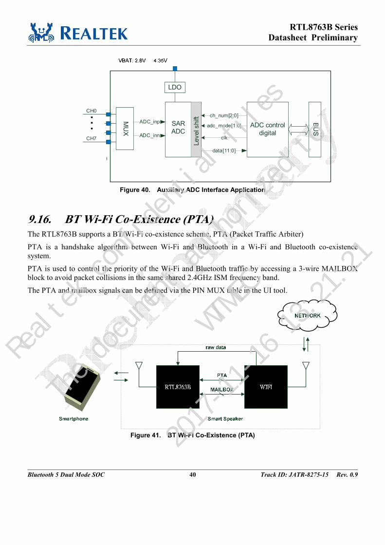
RTL8763B Series
Datasheet Preliminary
Bluetooth 5 Dual Mode SOC 40 Track ID: JATR-8275-15 Rev. 0.9
MU
X
LDO
VBAT:
1.62~5V
ch_num[2:0]
adc_mode[1:0]
clk
data[11:0]
ADC control
digital
BU
S
ADC_inp
ADC_inn
Input swing:
0~min(VBAT, 3.6V)
Level shift
CH7
CH1
CH0
SAR
ADCCH6
Figure 40. Auxiliary ADC Interface Application
9.16. BT Wi-Fi Co-Existence (PTA) The RTL8763B supports a BT/Wi-Fi co-existence scheme, PTA (Packet Traffic Arbiter)
PTA is a handshake algorithm between Wi-Fi and Bluetooth in a Wi-Fi and Bluetooth co-existence
system.
PTA is used to control the priority of the Wi-Fi and Bluetooth traffic by accessing a 3-wire MAILBOX
block to avoid packet collisions in the same shared 2.4GHz ISM frequency band.
The PTA and mailbox signals can be defined via the PIN MUX table in the UI tool.
Figure 41. BT Wi-Fi Co-Existence (PTA)
Realtek confidential files
The document authorized to
WTMEC
2017-11-16 13:21:21
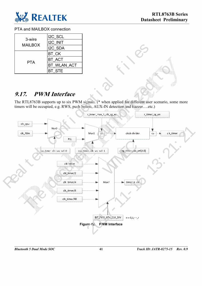
RTL8763B Series
Datasheet Preliminary
Bluetooth 5 Dual Mode SOC 41 Track ID: JATR-8275-15 Rev. 0.9
PTA and MAILBOX connection
9.17. PWM Interface The RTL8763B supports up to six PWM signals. (* when applied for different user scenario, some more
timers will be occupied, e.g. RWS, push button, AUX-IN detection and buzzer….etc.)
Figure 42. PWM Interface
I2C_SCL
I2C_INIT
I2C_SDA
BT_CK
BT_ACT
BT_WLAN_ACT
BT_STE
3-wire
MAILBOX
PTA
Realtek confidential files
The document authorized to
WTMEC
2017-11-16 13:21:21
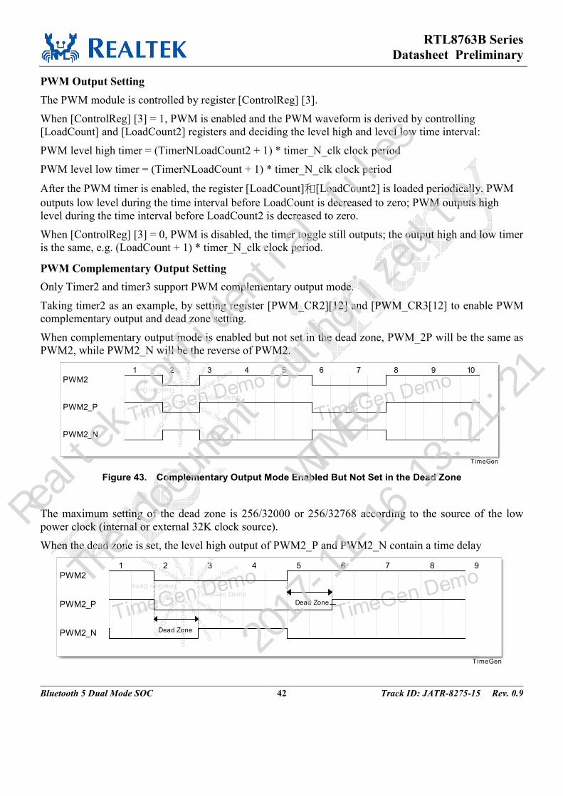
RTL8763B Series
Datasheet Preliminary
Bluetooth 5 Dual Mode SOC 42 Track ID: JATR-8275-15 Rev. 0.9
PWM Output Setting
The PWM module is controlled by register [ControlReg] [3].
When [ControlReg] [3] = 1, PWM is enabled and the PWM waveform is derived by controlling
[LoadCount] and [LoadCount2] registers and deciding the level high and level low time interval:
PWM level high timer = (TimerNLoadCount2 + 1) * timer_N_clk clock period
PWM level low timer = (TimerNLoadCount + 1) * timer_N_clk clock period
After the PWM timer is enabled, the register [LoadCount]和[LoadCount2] is loaded periodically. PWM
outputs low level during the time interval before LoadCount is decreased to zero; PWM outputs high
level during the time interval before LoadCount2 is decreased to zero.
When [ControlReg] [3] = 0, PWM is disabled, the timer toggle still outputs; the output high and low timer
is the same, e.g. (LoadCount + 1) * timer_N_clk clock period.
PWM Complementary Output Setting
Only Timer2 and timer3 support PWM complementary output mode.
Taking timer2 as an example, by setting register [PWM_CR2][12] and [PWM_CR3[12] to enable PWM
complementary output and dead zone setting.
When complementary output mode is enabled but not set in the dead zone, PWM_2P will be the same as
PWM2, while PWM2_N will be the reverse of PWM2.
Figure 43. Complementary Output Mode Enabled But Not Set in the Dead Zone
The maximum setting of the dead zone is 256/32000 or 256/32768 according to the source of the low
power clock (internal or external 32K clock source).
When the dead zone is set, the level high output of PWM2_P and PWM2_N contain a time delay
TimeGen Demo
TimeGen Demo 1 2 3 4 5 6 7 8 9 10
TimeGen Demo Tim
eGen Demo
Tim
eG
en D
emo
Tim
eG
en
De
mo
Tim
eG
en D
emo
Tim
eGen Demo
TimeGen Demo TimeGen Demo T
imeG
en D
emo
Tim
eG
en
De
mo
Tim
eG
en D
emo
TimeGen Demo
TimeGen
PWM2
PWM2_P
PWM2_N
TimeGen Demo
TimeGen Demo 1 2 3 4 5 6 7 8 9
TimeGen Demo Tim
eGen Demo
Tim
eG
en D
emo
Tim
eG
en
De
mo
Tim
eG
en D
emo
Tim
eGen Demo
TimeGen Demo TimeGen Demo
Tim
eG
en D
emo
Tim
eG
en
De
mo
Tim
eG
en D
emo
TimeGen Demo
Dead Zone
Dead Zone
TimeGen
PWM2
PWM2_P
PWM2_N
Realtek confidential files
The document authorized to
WTMEC
2017-11-16 13:21:21
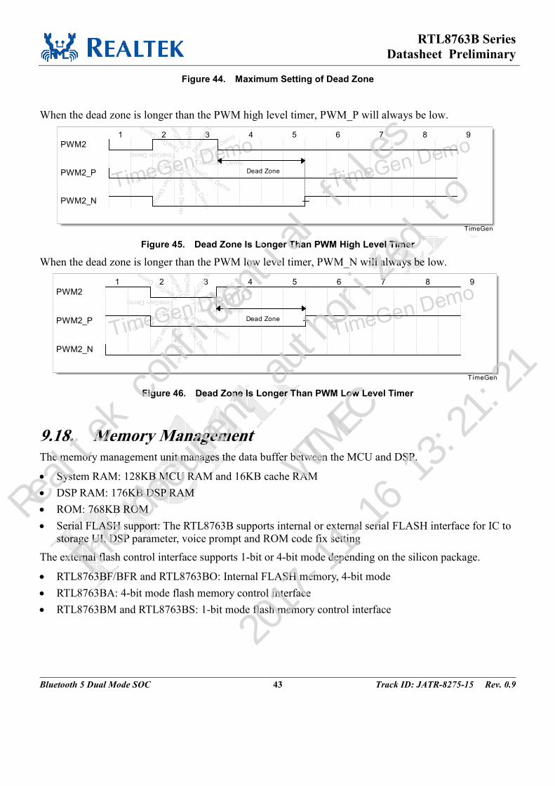
RTL8763B Series
Datasheet Preliminary
Bluetooth 5 Dual Mode SOC 43 Track ID: JATR-8275-15 Rev. 0.9
Figure 44. Maximum Setting of Dead Zone
When the dead zone is longer than the PWM high level timer, PWM_P will always be low.
Figure 45. Dead Zone Is Longer Than PWM High Level Timer
When the dead zone is longer than the PWM low level timer, PWM_N will always be low.
Figure 46. Dead Zone Is Longer Than PWM Low Level Timer
9.18. Memory Management The memory management unit manages the data buffer between the MCU and DSP.
• System RAM: 128KB MCU RAM and 16KB cache RAM
• DSP RAM: 176KB DSP RAM
• ROM: 768KB ROM
• Serial FLASH support: The RTL8763B supports internal or external serial FLASH interface for IC to
storage UI, DSP parameter, voice prompt and ROM code fix setting
The external flash control interface supports 1-bit or 4-bit mode depending on the silicon package.
• RTL8763BF/BFR and RTL8763BO: Internal FLASH memory, 4-bit mode
• RTL8763BA: 4-bit mode flash memory control interface
• RTL8763BM and RTL8763BS: 1-bit mode flash memory control interface
TimeGen Demo
TimeGen Demo 1 2 3 4 5 6 7 8 9
TimeGen Demo Tim
eGen Demo
Tim
eG
en D
emo
Tim
eG
en
De
mo
Tim
eG
en D
emo
Tim
eGen Demo
TimeGen Demo TimeGen Demo
Tim
eG
en D
emo
Tim
eG
en
De
mo
Tim
eG
en D
emo
TimeGen Demo
Dead Zone
TimeGen
PWM2
PWM2_P
PWM2_N
TimeGen Demo
TimeGen Demo 1 2 3 4 5 6 7 8 9
TimeGen Demo Tim
eGen Demo
Tim
eG
en D
emo
Tim
eG
en
De
mo
Tim
eG
en D
emo
Tim
eGen Demo
TimeGen Demo TimeGen Demo
Tim
eG
en D
emo
Tim
eG
en
De
mo
Tim
eG
en D
emo
TimeGen Demo
Dead Zone
TimeGen
PWM2
PWM2_P
PWM2_N
Realtek confidential files
The document authorized to
WTMEC
2017-11-16 13:21:21
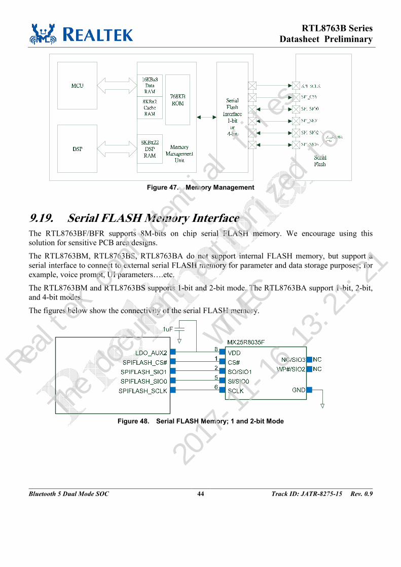
RTL8763B Series
Datasheet Preliminary
Bluetooth 5 Dual Mode SOC 44 Track ID: JATR-8275-15 Rev. 0.9
Figure 47. Memory Management
9.19. Serial FLASH Memory Interface The RTL8763BF/BFR supports 8M-bits on chip serial FLASH memory. We encourage using this
solution for sensitive PCB area designs.
The RTL8763BM, RTL8763BS, RTL8763BA do not support internal FLASH memory, but support a
serial interface to connect to external serial FLASH memory for parameter and data storage purposes; for
example, voice prompt, UI parameters….etc.
The RTL8763BM and RTL8763BS supports 1-bit and 2-bit mode. The RTL8763BA support 1-bit, 2-bit,
and 4-bit modes.
The figures below show the connectivity of the serial FLASH memory.
Figure 48. Serial FLASH Memory; 1 and 2-bit Mode
Realtek confidential files
The document authorized to
WTMEC
2017-11-16 13:21:21
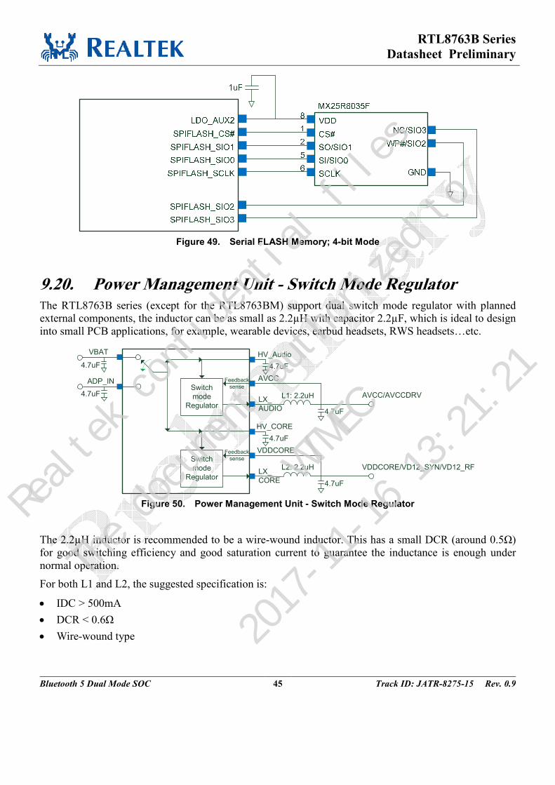
RTL8763B Series
Datasheet Preliminary
Bluetooth 5 Dual Mode SOC 45 Track ID: JATR-8275-15 Rev. 0.9
Figure 49. Serial FLASH Memory; 4-bit Mode
9.20. Power Management Unit - Switch Mode Regulator The RTL8763B series (except for the RTL8763BM) support dual switch mode regulator with planned
external components, the inductor can be as small as 2.2µH with capacitor 2.2µF, which is ideal to design
into small PCB applications, for example, wearable devices, earbud headsets, RWS headsets…etc.
Switch
mode
Regulator
VBAT
ADP_IN
HV_Audio
LX_
AUDIO
L1: 2.2uH
4.7uF
4.7uF
AVCC/AVCCDRV
AVCCFeedback
sense
4.7uF
4.7uF
Switch
mode
Regulator
HV_CORE
LX_
CORE 4.7uF
4.7uF
VDDCORE/VD12_SYN/VD12_RF
VDDCOREFeedback
sense
L2: 2.2uH
Figure 50. Power Management Unit - Switch Mode Regulator
The 2.2µH inductor is recommended to be a wire-wound inductor. This has a small DCR (around 0.5Ω)
for good switching efficiency and good saturation current to guarantee the inductance is enough under
normal operation.
For both L1 and L2, the suggested specification is:
• IDC > 500mA
• DCR < 0.6Ω
• Wire-wound type
Realtek confidential files
The document authorized to
WTMEC
2017-11-16 13:21:21
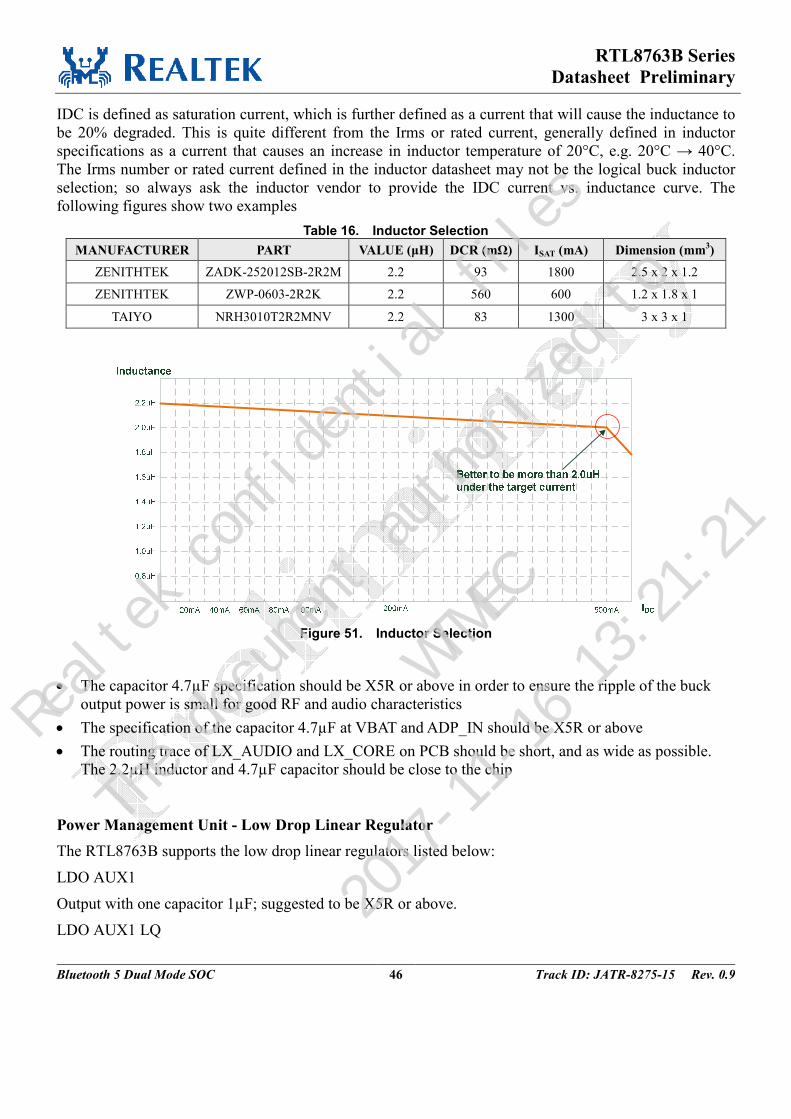
RTL8763B Series
Datasheet Preliminary
Bluetooth 5 Dual Mode SOC 46 Track ID: JATR-8275-15 Rev. 0.9
IDC is defined as saturation current, which is further defined as a current that will cause the inductance to
be 20% degraded. This is quite different from the Irms or rated current, generally defined in inductor
specifications as a current that causes an increase in inductor temperature of 20°C, e.g. 20°C → 40°C.
The Irms number or rated current defined in the inductor datasheet may not be the logical buck inductor
selection; so always ask the inductor vendor to provide the IDC current vs. inductance curve. The
following figures show two examples
Table 16. Inductor Selection
MANUFACTURER PART VALUE (µH) DCR (mΩ) ISAT (mA) Dimension (mm3)
ZENITHTEK ZADK-252012SB-2R2M 2.2 93 1800 2.5 x 2 x 1.2
ZENITHTEK ZWP-0603-2R2K 2.2 560 600 1.2 x 1.8 x 1
TAIYO NRH3010T2R2MNV 2.2 83 1300 3 x 3 x 1
Figure 51. Inductor Selection
• The capacitor 4.7µF specification should be X5R or above in order to ensure the ripple of the buck
output power is small for good RF and audio characteristics
• The specification of the capacitor 4.7µF at VBAT and ADP_IN should be X5R or above
• The routing trace of LX_AUDIO and LX_CORE on PCB should be short, and as wide as possible.
The 2.2µH inductor and 4.7µF capacitor should be close to the chip
Power Management Unit - Low Drop Linear Regulator
The RTL8763B supports the low drop linear regulators listed below:
LDO AUX1
Output with one capacitor 1µF; suggested to be X5R or above.
LDO AUX1 LQ
Realtek confidential files
The document authorized to
WTMEC
2017-11-16 13:21:21
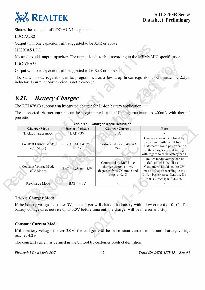
RTL8763B Series
Datasheet Preliminary
Bluetooth 5 Dual Mode SOC 47 Track ID: JATR-8275-15 Rev. 0.9
Shares the same pin of LDO AUX1 as pin out.
LDO AUX2
Output with one capacitor 1µF; suggested to be X5R or above.
MICBIAS LDO
No need to add output capacitor. The output is adjustable according to the MEMs MIC specification.
LDO VPA33
Output with one capacitor 1µF; suggested to be X5R or above.
The switch mode regulator can be programmed as a low drop linear regulator to eliminate the 2.2µH
inductor if current consumption is not a concern.
9.21. Battery Charger The RTL8763B supports an integrated charger for Li-Ion battery application.
The supported charger current can be programmed in the UI tool; maximum is 400mA with thermal
protection.
Table 17. Charger Mode Definition
Charger Mode Battery Voltage Charger Current Note
Trickle charger mode BAT < 3V 0.1C -
Constant Current Mode
(CC Mode)
3.0V ≤ BAT ≤ 4.2V or
4.35V
Customer defined; 400mA
max.
Charger current is defined by
customer with the UI tool.
Customers should pay attention
to the charger current setting
with regard to their battery pack.
Constant Voltage Mode
(CV Mode) BAT = 4.2V or 4.35V
Controlled by MCU, the
charger current slowly
degrades from CC mode and
stops at 0.1C
The CV mode voltage can be
defined with the UI tool.
Customers should set the CV
mode voltage according to the
Li-Ion battery specification. Do
not set over specification.
Re-Charge Mode BAT ≤ 4.0V - -
Trickle Charger Mode
If the battery voltage is below 3V, the charger will charge the battery with a low current of 0.1C. If the
battery voltage does not rise up to 3.0V before time out, the charger will be in error and stop.
Constant Current Mode
If the battery voltage is over 3.0V, the charger will be in constant current mode until battery voltage
reaches 4.2V.
The constant current is defined in the UI tool by customer product definition.
Realtek confidential files
The document authorized to
WTMEC
2017-11-16 13:21:21
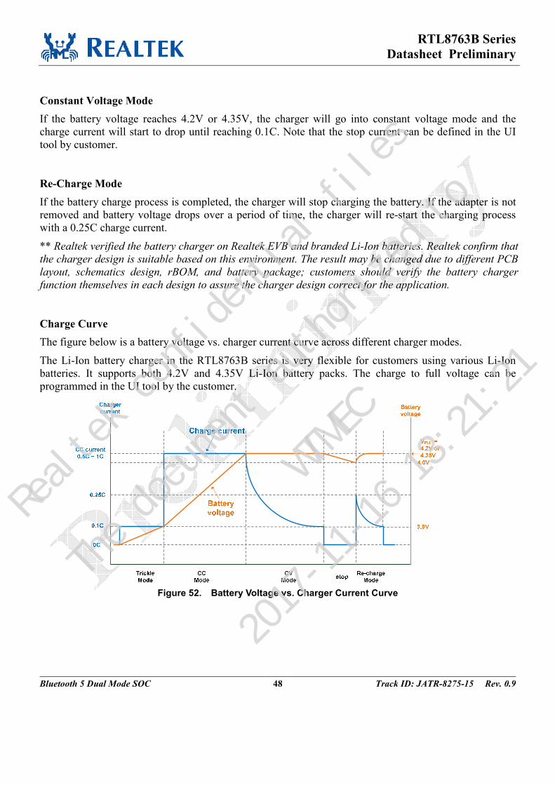
RTL8763B Series
Datasheet Preliminary
Bluetooth 5 Dual Mode SOC 48 Track ID: JATR-8275-15 Rev. 0.9
Constant Voltage Mode
If the battery voltage reaches 4.2V or 4.35V, the charger will go into constant voltage mode and the
charge current will start to drop until reaching 0.1C. Note that the stop current can be defined in the UI
tool by customer.
Re-Charge Mode
If the battery charge process is completed, the charger will stop charging the battery. If the adapter is not
removed and battery voltage drops over a period of time, the charger will re-start the charging process
with a 0.25C charge current.
** Realtek verified the battery charger on Realtek EVB and branded Li-Ion batteries. Realtek confirm that
the charger design is suitable based on this environment. The result may be changed due to different PCB
layout, schematics design, rBOM, and battery package; customers should verify the battery charger
function themselves in each design to assure the charger design correct for the application.
Charge Curve
The figure below is a battery voltage vs. charger current curve across different charger modes.
The Li-Ion battery charger in the RTL8763B series is very flexible for customers using various Li-Ion
batteries. It supports both 4.2V and 4.35V Li-Ion battery packs. The charge to full voltage can be
programmed in the UI tool by the customer.
Figure 52. Battery Voltage vs. Charger Current Curve
Realtek confidential files
The document authorized to
WTMEC
2017-11-16 13:21:21
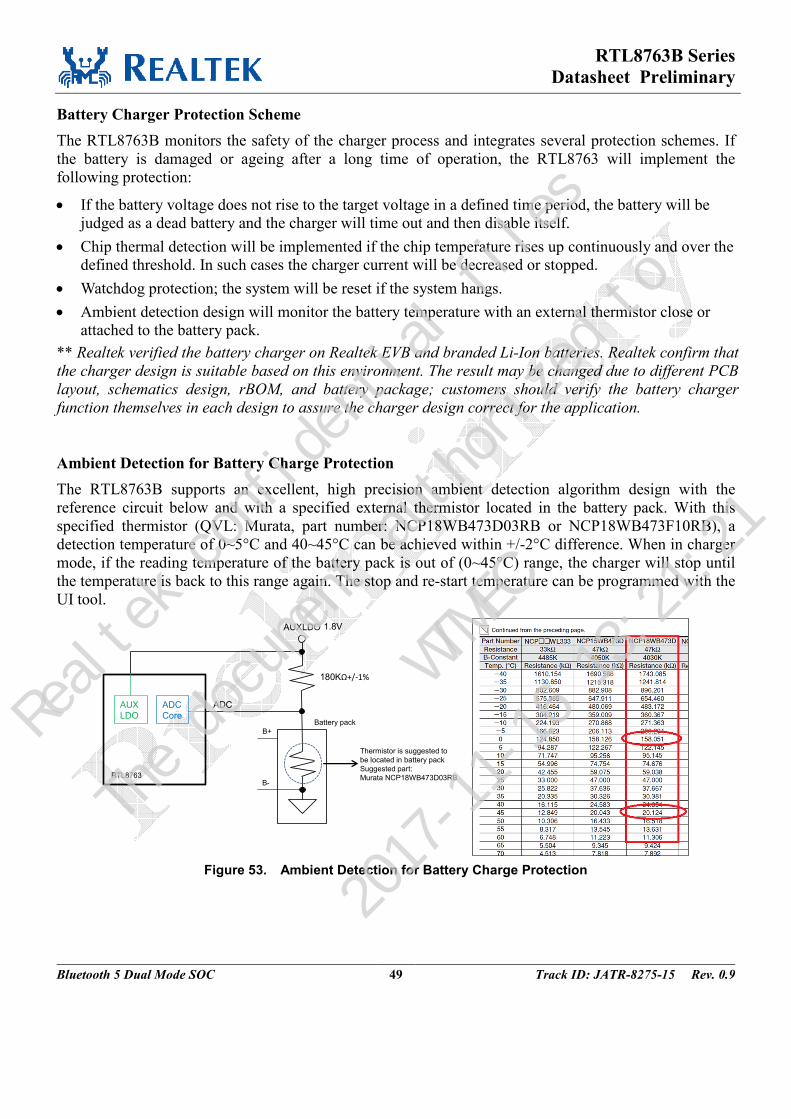
RTL8763B Series
Datasheet Preliminary
Bluetooth 5 Dual Mode SOC 49 Track ID: JATR-8275-15 Rev. 0.9
Battery Charger Protection Scheme
The RTL8763B monitors the safety of the charger process and integrates several protection schemes. If
the battery is damaged or ageing after a long time of operation, the RTL8763 will implement the
following protection:
• If the battery voltage does not rise to the target voltage in a defined time period, the battery will be
judged as a dead battery and the charger will time out and then disable itself.
• Chip thermal detection will be implemented if the chip temperature rises up continuously and over the
defined threshold. In such cases the charger current will be decreased or stopped.
• Watchdog protection; the system will be reset if the system hangs.
• Ambient detection design will monitor the battery temperature with an external thermistor close or
attached to the battery pack.
** Realtek verified the battery charger on Realtek EVB and branded Li-Ion batteries. Realtek confirm that
the charger design is suitable based on this environment. The result may be changed due to different PCB
layout, schematics design, rBOM, and battery package; customers should verify the battery charger
function themselves in each design to assure the charger design correct for the application.
Ambient Detection for Battery Charge Protection
The RTL8763B supports an excellent, high precision ambient detection algorithm design with the
reference circuit below and with a specified external thermistor located in the battery pack. With this
specified thermistor (QVL: Murata, part number: NCP18WB473D03RB or NCP18WB473F10RB), a
detection temperature of 0~5°C and 40~45°C can be achieved within +/-2°C difference. When in charger
mode, if the reading temperature of the battery pack is out of (0~45°C) range, the charger will stop until
the temperature is back to this range again. The stop and re-start temperature can be programmed with the
UI tool.
ADC
Core
AUXLDO 1.8V
180KΩ+/-1%
AUX
LDO
ADC
Battery pack
Thermistor is suggested to
be located in battery pack
Suggested part:
Murata NCP18WB473D03RB
B+
B-RTL8763
Figure 53. Ambient Detection for Battery Charge Protection
Realtek confidential files
The document authorized to
WTMEC
2017-11-16 13:21:21
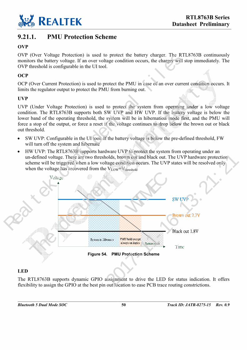
RTL8763B Series
Datasheet Preliminary
Bluetooth 5 Dual Mode SOC 50 Track ID: JATR-8275-15 Rev. 0.9
9.21.1. PMU Protection Scheme
OVP
OVP (Over Voltage Protection) is used to protect the battery charger. The RTL8763B continuously
monitors the battery voltage. If an over voltage condition occurs, the charger will stop immediately. The
OVP threshold is configurable in the UI tool.
OCP
OCP (Over Current Protection) is used to protect the PMU in case of an over current condition occurs. It
limits the regulator output to protect the PMU from burning out.
UVP
UVP (Under Voltage Protection) is used to protect the system from operating under a low voltage
condition. The RTL8763B supports both SW UVP and HW UVP. If the battery voltage is below the
lower band of the operating threshold, the system will be in hibernation mode first, and the PMU will
force a stop of the output, or force a reset if the voltage continues to drop below the brown out or black
out threshold.
• SW UVP: Configurable in the UI tool. If the battery voltage is below the pre-defined threshold, FW
will turn off the system and hibernate
• HW UVP: The RTL8763B supports hardware UVP to protect the system from operating under an
un-defined voltage. There are two thresholds, brown out and black out. The UVP hardware protection
scheme will be triggered when a low voltage condition occurs. The UVP states will be resolved only
when the voltage has recovered from the VLOW+Vthreshold
Figure 54. PMU Protection Scheme
LED
The RTL8763B supports dynamic GPIO assignment to drive the LED for status indication. It offers
flexibility to assign the GPIO at the best pin out location to ease PCB trace routing constrictions.
Realtek confidential files
The document authorized to
WTMEC
2017-11-16 13:21:21
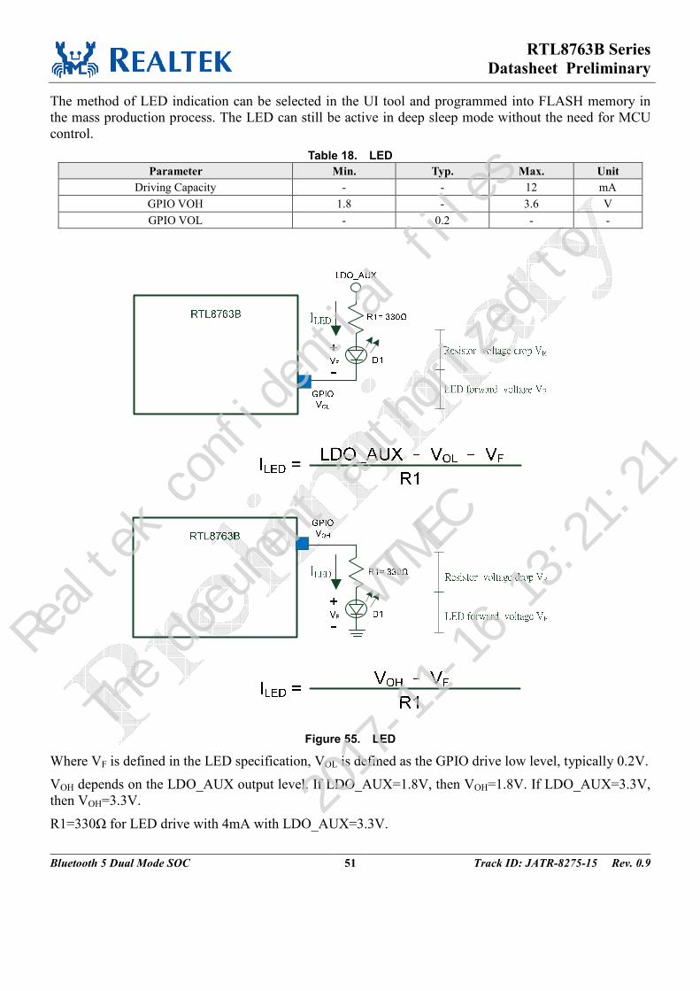
RTL8763B Series
Datasheet Preliminary
Bluetooth 5 Dual Mode SOC 51 Track ID: JATR-8275-15 Rev. 0.9
The method of LED indication can be selected in the UI tool and programmed into FLASH memory in
the mass production process. The LED can still be active in deep sleep mode without the need for MCU
control.
Table 18. LED
Parameter Min. Typ. Max. Unit
Driving Capacity - - 12 mA
GPIO VOH 1.8 - 3.6 V
GPIO VOL - 0.2 - -
Figure 55. LED
Where VF is defined in the LED specification, VOL is defined as the GPIO drive low level, typically 0.2V.
VOH depends on the LDO_AUX output level. If LDO_AUX=1.8V, then VOH=1.8V. If LDO_AUX=3.3V,
then VOH=3.3V.
R1=330Ω for LED drive with 4mA with LDO_AUX=3.3V.
Realtek confidential files
The document authorized to
WTMEC
2017-11-16 13:21:21
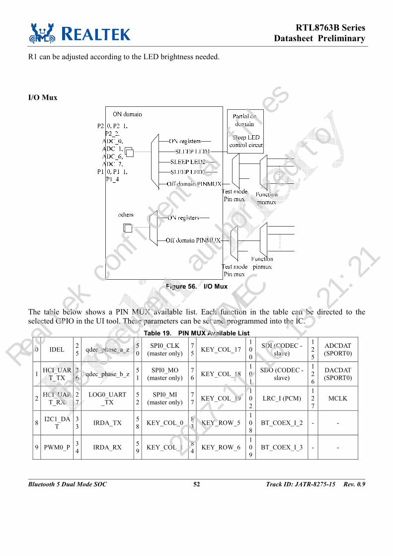
RTL8763B Series
Datasheet Preliminary
Bluetooth 5 Dual Mode SOC 52 Track ID: JATR-8275-15 Rev. 0.9
R1 can be adjusted according to the LED brightness needed.
I/O Mux
Figure 56. I/O Mux
The table below shows a PIN MUX available list. Each function in the table can be directed to the
selected GPIO in the UI tool. These parameters can be set and programmed into the IC.
Table 19. PIN MUX Available List
0 IDEL 2
5 qdec_phase_a_z
5
0
SPI0_CLK
(master only)
7
5 KEY_COL_17
1
0
0
SDI (CODEC -
slave)
1
2
5
ADCDAT
(SPORT0)
1 HCI_UAR
T_TX
2
6 qdec_phase_b_z
5
1
SPI0_MO
(master only)
7
6 KEY_COL_18
1
0
1
SDO (CODEC -
slave)
1
2
6
DACDAT
(SPORT0)
2 HCI_UAR
T_RX
2
7
LOG0_UART
_TX
5
2
SPI0_MI
(master only)
7
7 KEY_COL_19
1
0
2
LRC_I (PCM)
1
2
7
MCLK
8 I2C1_DA
T
3
3 IRDA_TX
5
8 KEY_COL_0
8
3 KEY_ROW_5
1
0
8
BT_COEX_I_2 - -
9 PWM0_P 3
4 IRDA_RX
5
9 KEY_COL_1
8
4 KEY_ROW_6
1
0
9
BT_COEX_I_3 - -
Realtek confidential files
The document authorized to
WTMEC
2017-11-16 13:21:21
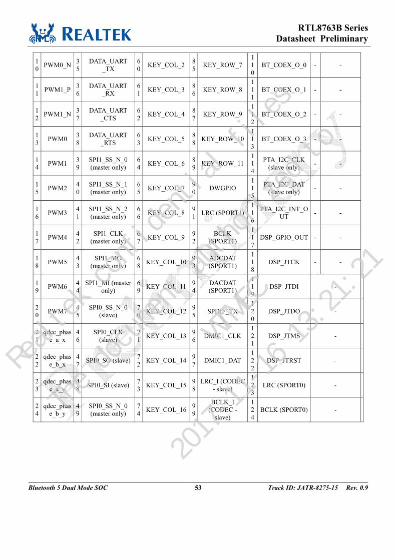
RTL8763B Series
Datasheet Preliminary
Bluetooth 5 Dual Mode SOC 53 Track ID: JATR-8275-15 Rev. 0.9
1
0 PWM0_N
3
5
DATA_UART
_TX
6
0 KEY_COL_2
8
5 KEY_ROW_7
1
1
0
BT_COEX_O_0 - -
1
1 PWM1_P
3
6
DATA_UART
_RX
6
1 KEY_COL_3
8
6 KEY_ROW_8
1
1
1
BT_COEX_O_1 - -
1
2 PWM1_N
3
7
DATA_UART
_CTS
6
2 KEY_COL_4
8
7 KEY_ROW_9
1
1
2
BT_COEX_O_2 - -
1
3 PWM0
3
8
DATA_UART
_RTS
6
3 KEY_COL_5
8
8 KEY_ROW_10
1
1
3
BT_COEX_O_3 - -
1
4 PWM1
3
9
SPI1_SS_N_0
(master only)
6
4 KEY_COL_6
8
9 KEY_ROW_11
1
1
4
PTA_I2C_CLK
(slave only) - -
1
5 PWM2
4
0
SPI1_SS_N_1
(master only)
6
5 KEY_COL_7
9
0 DWGPIO
1
1
5
PTA_I2C_DAT
(slave only) - -
1
6 PWM3
4
1
SPI1_SS_N_2
(master only)
6
6 KEY_COL_8
9
1 LRC (SPORT1)
1
1
6
PTA_I2C_INT_O
UT - -
1
7 PWM4
4
2
SPI1_CLK
(master only)
6
7 KEY_COL_9
9
2
BCLK
(SPORT1)
1
1
7
DSP_GPIO_OUT - -
1
8 PWM5
4
3
SPI1_MO
(master only)
6
8 KEY_COL_10
9
3
ADCDAT
(SPORT1)
1
1
8
DSP_JTCK - -
1
9 PWM6
4
4
SPI1_MI (master
only)
6
9 KEY_COL_11
9
4
DACDAT
(SPORT1)
1
1
9
DSP_JTDI -
2
0 PWM7
4
5
SPI0_SS_N_0
(slave)
7
0 KEY_COL_12
9
5 SPDIF_TX
1
2
0
DSP_JTDO -
2
1
qdec_phas
e_a_x
4
6
SPI0_CLK
(slave)
7
1 KEY_COL_13
9
6 DMIC1_CLK
1
2
1
DSP_JTMS -
2
2
qdec_phas
e_b_x
4
7 SPI0_SO (slave)
7
2 KEY_COL_14
9
7 DMIC1_DAT
1
2
2
DSP_JTRST -
2
3
qdec_phas
e_a_y
4
8 SPI0_SI (slave)
7
3 KEY_COL_15
9
8
LRC_I (CODEC
- slave)
1
2
3
LRC (SPORT0) -
2
4
qdec_phas
e_b_y
4
9
SPI0_SS_N_0
(master only)
7
4 KEY_COL_16
9
9
BCLK_I
(CODEC -
slave)
1
2
4
BCLK (SPORT0) -
Realtek confidential files
The document authorized to
WTMEC
2017-11-16 13:21:21
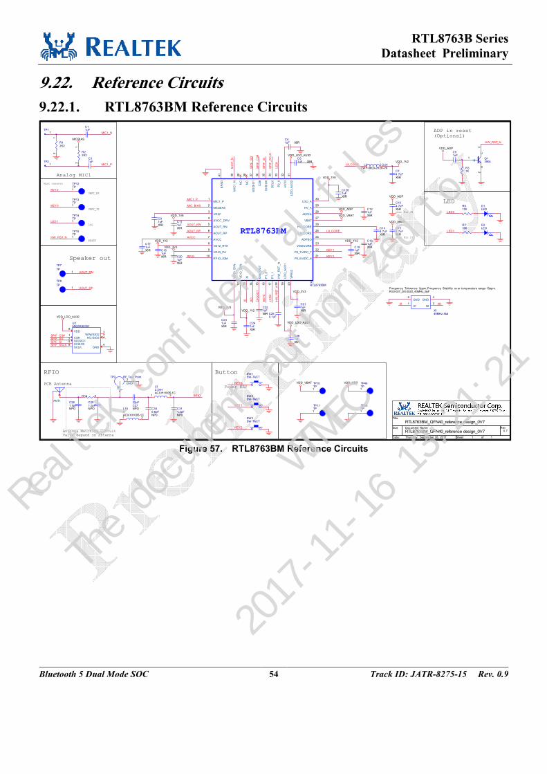
RTL8763B Series
Datasheet Preliminary
Bluetooth 5 Dual Mode SOC 54 Track ID: JATR-8275-15 Rev. 0.9
9.22. Reference Circuits
9.22.1. RTL8763BM Reference Circuits
Figure 57. RTL8763BM Reference Circuits
Power KEY
Title
Size Document Name Rev
Date: Sheet of
RTL8763BM_QFN40_reference design_0V7 0.7
RTL8763BM_QFN40_reference design_0V7
REALTEK Semiconductor Corp.
Addr: No.2, Innovation Rd. II, Hsinchu Science Park, Hsinchu 30076, Taiwan
TEL: 886-3-5780211
1 1Thursday , September 28, 2017
KEY1
MIC1_N
MIC1_P LX_CORE
KEY0
LX_CORE
KE
Y0
AVCC
HW
_R
ST
_N
LE
D0
AOUT_RP
LE
D1
RFIOD
IGO
UT
RFIO
XOXI
AOUT_RN
KEY2
KEY1X
O
XI
AOUT_RP
AOUT_RN
LED0
HW_RST_N
LED1
HW_RST_N
LED1
KEY 0
KEY 2
SP
IF_S
O
SP
IF_C
S#
SP
IF_S
I
SP
IF_S
CL
K
MIC
1_
N
MIC1_P
MIC_BIAS
TP12TP1
KEY2
C51uF
R7100
C231uFX5R
TP14TP1
C281.5pFNPO
C74.7uFX5R
C191uFX5R
TP8
TP1
L32.2nHACX HI1005-1C
1 2
C121uFX5R
C11uF
R12K2
12
ANT1
C261uFX5R
C111uFX5R
C311.2pFNP0
C181uFX5R
C241uFX5R
C144.7uFX5R
SW1SW-TACT
R31K
TP9 RF Test Point
RF
1
2
GND
C91uFX5R
L2 2.2uHZWP-0603-2R2K-V0
D2LED
X140MHz Xtal
Frequency Tolerence: 5ppm;Frequency Stability ov er temperature range:15ppm.R53-027_SX-2520_40MHz_9pF
X11
GND2
GND4
X23
TP15TP1
C291.5pFNPO
C41uF X5R
TP13TP1
RTL8763BM
U1RTL8763BM
MIC1_P1
MICBIAS2
VREF3
AVCC_DRV4
AOUT_RN5
AOUT_RP6
AVCC7
VD12_RTX8
VD33_PA9
RFIO_IQM10
VD
33
_S
YN
11
VD
12
_S
YN
12
XI
13
XO
14
DIG
_O
UT
15
P1_
016
P1_
117
HW
_R
ST
_N
18
LD
O_
AU
X1
19
VP
A3
320
LDO_A30
HV_A29
ADPIN28
VBAT27
HV_CORE26
LX_CORE25
ADPSO24
VDDCORE23
P0_7/ADC_722
P0_6/ADC_621
MIC
1_N
40
NC
39
NC
38
SO
/SIO
137
CS
#36
SI/
SIO
035
SC
LK
34
P2_
033
HV
33
32
LD
O_A
UX
231
EP
AD
41
R22K2
12
C61uF X5R
C171uFX5R
C161uFX5R
TP10TP1
R6100
Q13904B
1
C3
E2
C104.7uFX5R
C300.6pFNP0
C154.7uFX5R
C31uF
TP11
C2722pF
NPO
C221uFX5R
TP21
TP11TP1
C250.1uF
SW3SW-TACT
D1LED
TP7
TP1
C201uFX5R
SW2SW-TACT
R14 0
C211uFX5R
MICBIAS
VDD_VBAT
VDD_1V2
VDD_3V3
VDD_ADP
VDD_VBAT
VDD_1V2
VDD_1V2
VDD_1V2
VDD_LDO_AUX2
VDD_ADP
VDD_VBAT
VDD_3V3
VDD_ADP
VDD_3V3
VDD_LDO_AUX1
VDD_1V8
PCB Antenna
Analog MIC1
Button
Antenna Matching CircuitValue depand on Antenna
LED
Speaker out
ADP in reset(Optional)
near Pin 27
near Pin 28
RFIO
RESET
Must reserve
LOG
UART_TX
UART_RX
SPIF_SCLKSPIF_SISPIF_SOSPIF_CS#
U2MX25R8035F
VDD8
CS#1
SO/SIO12
SI/SIO05
NC/SIO37WP#/SIO23
SCLK6
GND4
VDD_LDO_AUX2
TP49TP1
TP50TP1
VDD_ADP
VDD_1V8
C1281uFX5R
L180ACX HI1005-1C1 2
Realtek confidential files
The document authorized to
WTMEC
2017-11-16 13:21:21
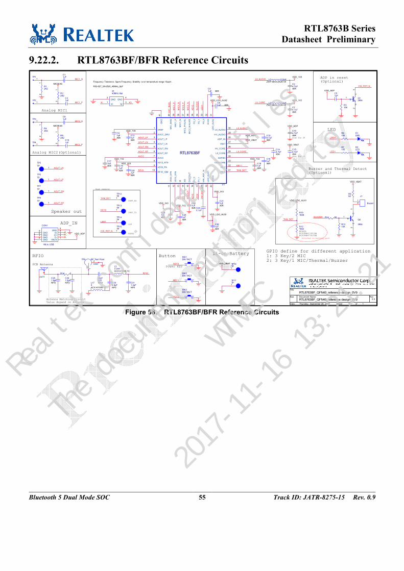
RTL8763B Series
Datasheet Preliminary
Bluetooth 5 Dual Mode SOC 55 Track ID: JATR-8275-15 Rev. 0.9
9.22.2. RTL8763BF/BFR Reference Circuits
Figure 58. RTL8763BF/BFR Reference Circuits
Power KEY
Title
Size Document Name Rev
Date: Sheet of
RTL8763BF_QFN40_reference design_0V9 0.9
RTL8763BF_QFN40_reference design_0V9
REALTEK Semiconductor Corp.
Addr: No.2, Innovation Rd. II, Hsinchu Science Park, Hsinchu 30076, Taiwan
TEL: 886-3-5780211
1 1Thursday , September 28, 2017
KEY0
KEY1
MIC1_N
MIC1_P LX_CORE
LX_AUDIO
DIG
OU
T
LX_CORE
LX_AUDIO
KE
Y0
AVCC
XO
XI
HW
_R
ST
_N
LE
D0
AOUT_RP
KE
Y2
BU
ZZ
ER
LE
D1
RFIO
RFIO
XOXI
AOUT_RN
THM_DET
KEY1
HW_RST_N
MIC
_B
IAS
MIC
1_P
MIC
1_N
LED0
KEY2
AOUT_LP
AOUT_LN
MIC2_P
AOUT_RP
AOUT_RN
AOUT_LP
AOUT_LN
MIC
2_P
MIC
2_N
LED1
MIC2_N
THM_DETBUZZER
HW_RST_N
LED1
KEY0
THM_DET
C104.7uFX5R
C311.2pFNP0
C24.7uFX5R
TP8
TP1
TP11TP1
C181uFX5R
C261uFX5R
C241uFX5R
D2LED
C11uF
R42K2
12
C291.5pFNPO
L1 2.2uHZWP-0603-2R2K-V0
R12K2
12
C154.7uFX5R
C61uF X5R
C91uFX5R
C111uFX5R
TP15TP1
C231uFX5R
TP9 RF Test Point
RF
1
2
GND
X140MHz Xtal
Frequency Tolerence: 5ppm;Frequency Stability ov er temperature range:15ppm.
R53-027_SX-2520_40MHz_9pF
X11
GND2
GND4
X23
SW2SW-TACT
R14 0
R52K2
12
TP12TP1
C131uF
R310K
C201uFX5R
C161uFX5R
U1
RTL8763BF
VREF1
AVCC_DRV2
AOUT_RN5
MIC
1_N
38
MIC
2_
P/A
UX
L37
AOUT_RP6
AVCC7
VD12_RTX8
VD33_PA9
RFIO_IQM10
VD
12
_S
YN
12
VD
33
_S
YN
11
XI
13
XO
14
DIG
_O
UT
15
P1_
01
6
P1_
11
7
HW
_R
ST
_N
18
LD
O_A
UX
11
9
VP
A3
32
0
P0_621
P0_722
VDDCORE23
ADPSO24
LX_CORE25
HV_CORE26
VBAT27
ADP_IN28
HV_AUDIO29
LX_AUDIO30
LD
O_
AU
X2
31
HV
33
32
P2_0
33
P2_1
34
P2_2
35
MIC
2_N
/AU
XR
36
MIC
1_P
39
MIC
_B
IAS
40
AOUT_LN4
AOUT_LP3
GN
D41
SW3SW-TACT
J1
Buzzer
12
R1310K
C300.6pFNP0
C250.1uF
TP11
D1LED
TP41
C81uF
R850
C191uFX5R
C281.5pFNPO
TP21
TP7
TP1
C41uF X5R
TP14TP1
C221uFX5R
C144.7uFX5R
R6100
CON1
Micro USB
VBUS1D-2D+3ID4GND5
GND9
GND8
GND7
GND6
TP10TP1
C74.7uFX5R
L170ACX HI1005-1C1 2
C171uFX5R
R12THM
L32.2nHACX HI1005-1C
1 2
R7100
R22K2
12
C51uF
SW1SW-TACT
C2722pF
NPO
C124.7uFX5R
C31uF
TP6
TP1
R10180K
R11 50
C211uFX5R
Q13904B
1
C3
E2
TP31
ANT1
TP5
TP1
Q2
3904
B1
C3
E2
TP13TP1
L2 2.2uHZWP-0603-2R2K-V0
MICBIAS
VDD_1V8
VDD_VBAT
VDD_1V2
VDD_3V3
VDD_ADP
VDD_VBAT
VDD_1V2
VDD_1V2
VDD_LDO_AUX2
VDD_1V2
VDD_ADP
VDD_VBAT
VDD_ADP
VDD_3V3
VDD_1V8
MICBIAS
VDD_VBAT
VDD_LDO_AUX1
VDD_ADP
VDD_3V3
VDD_LDO_AUX1
near Pin 27
near Pin 28
RFIOLi-on Battery
PCB Antenna
Analog MIC1
Button
Buzzer and Thermal Detect(Optional)
Analog MIC2(Optional)
Antenna Matching CircuitValue depand on Antenna
LED
Speaker out
ADP in reset(Optional)
ADP_IN
RESET
Must reserve
LOG
UART_TX
UART_RX
Attached on battery pack
MURATANCP18WB473D03RBNCP18WB473F10RB
GPIO define for different application1: 3 Key/2 MIC2: 3 Key/1 MIC/Thermal/Buzzer
Realtek confidential files
The document authorized to
WTMEC
2017-11-16 13:21:21
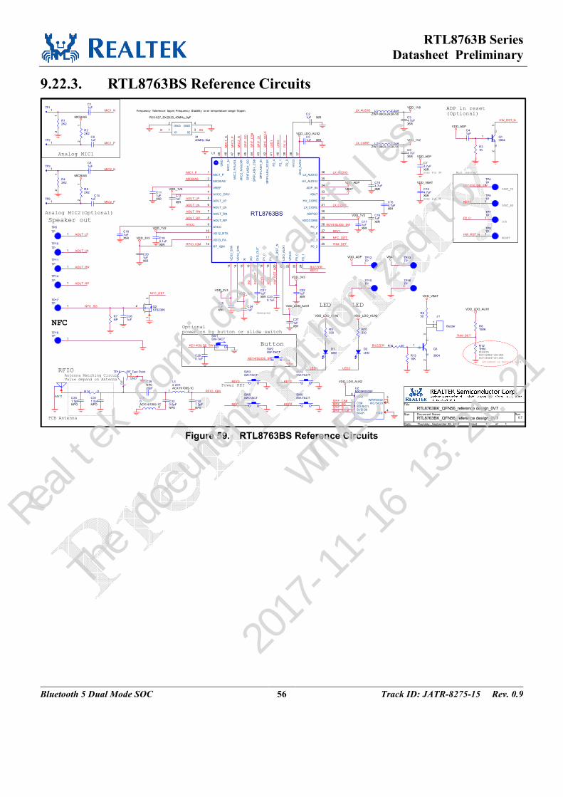
RTL8763B Series
Datasheet Preliminary
Bluetooth 5 Dual Mode SOC 56 Track ID: JATR-8275-15 Rev. 0.9
9.22.3. RTL8763BS Reference Circuits
Figure 59. RTL8763BS Reference Circuits
Power KEY
Title
Size Document Name Rev
Date: Sheet of
RTL8763BK_QFN56_reference design_0V7 0.7
RTL8763BK_QFN56_reference design_0V7
REALTEK Semiconductor Corp.
Addr: No.2, Innovation Rd. II, Hsinchu Science Park, Hsinchu 30076, Taiwan
TEL: 886-3-5780211
1 1Thursday , September 28, 2017
KEY0
MIC1_N
MIC1_P LX_CORE
LX_AUDIO
KEY4/SLIDE_SW
HW_RST_N
MIC2_N
MIC2_P
AOUT_RP
AOUT_RN
P2_0
KEY2
KEY0/SLIDE_SW
MIC
2_
N
MIC
2_
P
MIC
1_
N
KEY1
RFIO_IQM
MIC1_P
MICBIAS
HW_RST_N
AVCC
AOUT_RN
AOUT_RP
AOUT_LP
AOUT_LN
AOUT_LN
AOUT_LP
XO
XI
RFIO_IQM
HW
_R
ST
_N
KE
Y2
KE
Y0
DIG
OU
T
KEY4/SLIDE_SW
LX_CORE
LX_AUDIO
SP
IF_
SO
SP
IF_
CS
#
SP
IF_
SI
SP
IF_
SC
LK
SPIF_CS#
SPIF_SCLKSPIF_SISPIF_SO
KEY 1
NFC_DET
BUZZER
LED1
XOXI
THM_DET
LED2
NFC_DET
NFC_SG
KEY4/SLIDE_SW
P2
_0
KEY3
KEY2
LE
D2
LE
D1
KEY 3BUZZER
THM_DET
C261uF
TP13TP1
X140MHz Xtal
Frequency Tolerence: 5ppm;Frequency Stability ov er temperature range:15ppm.
R53-027_SX-2520_40MHz_9pF
X11
GND2
GND4
X23
R42K2
12
Q3
3904
B1
C3
E2
SW4SW-TACT
C241uF
C171uFX5R
C331.2pFNP0
U2MX25R8035F
VDD8
CS#1
SO/SIO12
SI/SIO05
NC/SIO37WP#/SIO23
SCLK6
GND4
C94.7uFX5R
ANT1
Q13904B
1
C3
E2
C51uF X5R
C61uF
C190.1uFX5R
U1
RTL8763BS
MIC1_P1
MICBIAS2
AOUT_LP5
SP
IFL
AS
H_
SO
45
SP
IFLA
SH
_C
S#
44
AOUT_LN6
AOUT_RN7
AOUT_RP8
AVCC9
VD12_RTX10
VD
12_
SY
N14
VD
33_
SY
N13
XI
15
XO
16
DIG
_O
UT
17
P1
_0
18
P1
_1
19
HW
_R
ST
_N
20
LD
O_A
UX
121
VP
A33
22
P0_225
P0_326
VDDCORE29
ADPSO30
LX_CORE31
HV_CORE32
VBAT33
ADP_IN34
HV_AUDIO35
LX_AUDIO36
LD
O_A
UX
23
7
HV
33
38
P2_
03
9
P2_
14
0
P2_
44
1
SP
IFLA
SH
_S
I4
3
MIC
2_
N/A
UX
R4
6
MIC
2_P
/AU
XL
47
AVCC_DRV4
VREF3
GN
D4
9
VD33_PA11
RF_IQM12
P0
_0
23
P0
_1
24
P0_627
P0_728
SP
IFLA
SH
_S
CL
K4
2
MIC
1_N
48
C211uFX5R
TP8
TP1
C181uFX5R
TP61
C81uF
L32.2nHACX HI1005-1C
1 2
R22K2
12
J1
Buzzer
12
SW2SW-TACT
C21uF X5R
TP11
TP1
TP9TP1
TP17TP
1
TP31
R9330
C29
20pFNP0
C141uF
C230.1uF
C320.6pFNP0
R11 50
R14 0
R12K2
12
R31K
C161uFX5R
C271uFX5R
C311.5pFNPO
D2
LED
C41uF
C131uFX5R
C111uFX5R
TP16TP1
SW6SW-TACT
TP4TP1
C301.5pFNPO
R12THM
R1310K
R52K2
12
L1 2.2uHZWP-0603-2R2K-V0
TP19 RF Test Point
RF
1
2
GND
C74.7uFX5R
C280.1uF
TP7TP1
C124.7uFX5R
C154.7uFX5R
R8180K
TP15TP1
TP5TP1
TP11
TP10
TP1
C201uFX5R
C104.7uFX5R
C221uFX5R
L2 2.2uHZWP-0603-2R2K-V0
R10330
TP12TP1
C11uF
TP14
TP1
R7NP
SW5SW-TACT
TP21
TP18TP
1SW1SW-TACT
R650
C34.7uFX5R
D1
LED
Q2STS2306
31
2
SW3SW-TACT
C251uFX5R
MICBIAS
VDD_1V2
VDD_1V8
VDD_ADP
VDD_VBAT
VDD_ADP
MICBIAS
VDD_LDO_AUX2
VDD_1V8
VDD_3V3
VDD_1V2
VDD_3V3
VDD_LDO_AUX1
VDD_1V2
VDD_3V3
VDD_ADP
VBAT
VDD_ADP
VDD_LDO_AUX2
VDD_1V2
VDD_LDO_AUX2
VBAT
VDD_LDO_AUX2
VDD_VBAT
VDD_LDO_AUX1
Speaker out
ADP in reset(Optional)
near Pin 38
near Pin 39
RFIO
PCB Antenna
Analog MIC1
Button
Attached on battery pack
MURATANCP18WB473D03RBNCP18WB473F10RB
LEDLEDReserved
RESET
Must reserve
LOG
UART_RX
UART_TX
Analog MIC2(Optional)
Antenna Matching CircuitValue depand on Antenna
NFCOptionalpower on by button or slide switch
L190ACX HI1005-1C1 2
Realtek confidential files
The document authorized to
WTMEC
2017-11-16 13:21:21
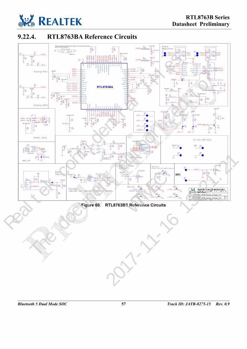
RTL8763B Series
Datasheet Preliminary
Bluetooth 5 Dual Mode SOC 57 Track ID: JATR-8275-15 Rev. 0.9
9.22.4. RTL8763BA Reference Circuits
Figure 60. RTL8763BS Reference Circuits
power key
Title
Size Document Name Rev
Date: Sheet of
RTL8763BA_QFN68_Speaker_ref design_1V0 1.0
RTL8763BA_QFN68_Speaker_ref design_1V0
REALTEK Semiconductor Corp.
Addr: No.2, Innovation Rd. II, Hsinchu Science Park, Hsinchu 30076, Taiwan
TEL: 886-3-5780211
C
1 1Thursday , September 28, 2017
MIC1_N
MIC1_P
LX_CORE
LX_AUDIO
AU
XIN
_L
AU
XIN
_R
US
B_D
M
US
B_D
P
BO
OS
T_
EN
LE
D2
AU
XIN
_D
ET
LE
D1
HW_RST_N
MIC2_N
MIC2_P
BOOST_EN
HW_RST_N
USB_DMUSB_DP
XO
KE
Y0
LX_AUDIO
KEY5
KEY4
NFC_DET
THM_DET
HV_AUDIO
MIC2_N
MIC1_N
HW
_R
ST
_N
KE
Y1
AN
T_
SW
AN
T_
SW
B
BU
ZZ
ER
AM
P_
EN
#
KE
Y2
KE
Y3
XI
SP
IF_
SIO
0
SP
IF_
SC
LK
RFIO_IQM
RFIO_TPM
AOUT_RP
AOUT_RN
MIC2_P
AOUT_LN
AOUT_LP
MIC1_P
XOXI
SP
IF_
SIO
3
SP
IF_
SIO
2
SP
IF_
SIO
1
SP
IF_
CS
#
AUXIN_R
AUXIN_L
KEY0
KEY1
NFC_SG
LED1
SLIDE_SW
OUT_RP
OUT_RN
OUT_LN
OUT_LP
SPIF_CS#
SPIF_SCLKSPIF_SIO0SPIF_SIO1
SPIF_SIO3SPIF_SIO2
AOUT_RP
AOUT_LP
G2
G1
SPK_O_R_P OUT_RN
OUT_RPSPK_O_R_N
SPK_O_L_P OUT_LP
OUT_LNSPK_O_L_N
NFC_DET
HW_RST_N
LED1
KEY0
KEY2
ANT_SWB
ANT_SW
RFIO_IQM
RFIO_TPM
BUZZER
THM_DET
KEY2
LED2
AUXIN_DET
AMP_EN#
KEY4
KEY5KEY3
LX_CORE
HV_CORE
G2
G1
C431uFX5R
D4LED
C61uF
R31200K
C3
4.7uF
>4.7uF, X5R
TP15TP1
R22 50
L3 BEAD1 2
C13 1uF
C34100uF
U2ALC105-VF
OUT_LP1
OUT_LN2
PVDD13
PVDD24
OUT_RN5
OUT_RP6
PD#7
BYPASS8
IN_R/DIFF+9
IN_L/DIFF-10
G111
G212
GN
D1
3
R7
10K
C5220pF
R2310K
TP121
C214.7uFX5R
L5 BEAD
1 2TP5
TP
1
R13
0
C4920pF
SW6SW-TACT
C291uFX5R
L10BEAD
1 2
C550.6pF
C4510pF
TP1
TP1
TP91
C481.2pF
C301uF
C571uF
C111uFTP6
1
C144.7uFX5R
R281K R27
20K
C4
680pF
R18330
C594.7uF
D3
LED
SW5SW-TACT
C16
0.1uF
C511.5pFNPO
U4
TRSW
RF11
GND2
RF23
VC24
RFC5
VC16
R16180K
C21uFX5R
R17
NP
U6APL3202
STAT1
GND2
BAT+3
VIN4
ISET5
R1550
CON1
USB_B TYPE
VBUS1D-2D+3ID4GND5
GND9
GND8
GND7
GND6
TP31
C5310pF
C234.7uFX5R
R4 0
R12
NC 0
C600.1uF
U5MX25R8035F
VDD8
CS#1
SO/SIO12
SI/SIO05
NC/SIO37WP#/SIO23
SCLK6
GND4
C281uFX5R
L1410uH-ZAH-70501 2
TP20TP1
L132.2nH
1 2
C58 1uF
R30600K
TP17TP1
C244.7uFX5R
L4 BEAD
1 2
D1
Schottky
TP8 1
R3
NC
R112K2
12
R25 0
TP2
TP 1
R2910K
L7BEAD
1 2
TP14TP1
C91uFX5R
C44
0.1uF
C470.4pF
SW7SW-TACT
C351uFX5R
L12.2uH
ZWP-0603-2R2K-V0
C10
4.7uF
>4.7uF, X5R
C19 2.2uF
SW2SW-TACT
TP4
TP
1
C5
680pF
R22K2
12
C8
680pF
Q3STS2306
31
2
C561.2pF
C391uFX5R
C614.7uF
C271uFX5R
L11BEAD1 2
C6210uF
C3210uF
TP16TP1
C11uFX5R
C4620pF
C541uF
ANT1
TP10 1
L8NC1 2
C7
680pF
R8
10K
R21THM
C221uFX5R
TP21TP
1
C12
0.33uF
L2 BEAD1 2
J1
Buzzer
12
L9BEAD1 2
TP7 1
TP22TP
1
R9
NC 0
Q2STS2306
31
2
R10
0
C37 1uF/X5R
R6
NC
R5 0
C38 1uF/X5R
R12K2
12
R19330
C401uFX5R
C311uF
C411uFX5R
X140MHz Xtal
Frequency Tolerence: 5ppm;Frequency Stability ov er temperature range:15ppm.R53-027_SX-2520_40MHz_9pF
X11
GND2
GND4
X23
RTL8763BA
MIC2_N1
MIC1_N3
MIC1_P4
MICBIAS5
VREF6
AVCC_DRV7
AOUT_LP8
AOUT_LN9
AOUT_RN10
VD12_PA13
VD
12_
SY
N1
9
VD
33_
SY
N1
8
XI
20
XO
21
DIG
_O
UT
22
P1
_0
23
P1
_3
26
P1
_4
27
P1
_5
28
P1
_6
29
32K_XO42
32K_XI43
ADPSO45
LX_CORE46
HV_CORE47
VBAT48
ADPIN49
HV_AUDIO50
LX_AUDIO51L
DO
_A
UX
25
2
HV
33
53
P2_
25
6
P2_
35
7
V33
_U
SB
64
DP
65
RFIO_TPM14
VD12_RTX15
VD33_PA16
RFIO_IQM17
44VDDCORE
P1
_7
30
HW
_R
ST
_N
31
LD
O_A
UX
13
2
VP
A33
33
P0_236
P0_337
P0_438
P0_539
DM
66
AU
XIN
_R
67
AU
XIN
_L
68
MIC2_P2
AOUT_RP11
AVCC12
P1
_1
24
P1
_2
25
P0
_0
34
P0_135
P0_640
P0_741
GN
D6
9
P2_
05
4
P2_
15
5
SP
IFLA
SH
_W
P#
/SIO
26
3
SP
IFLA
SH
_S
O/S
IO1
62
SP
IFL
AS
H_C
S#
61
SP
IFLA
SH
_S
I/S
IO0
60
SP
IFLA
SH
_S
CL
K5
9
SP
IFLA
SH
_H
OL
D#
/SIO
35
8
TP18TP1
D2
LED
U7APW7237
LX1
GND2
FB3
EN4
VIN5
C15
10uF
C18 1uF
C501.5pFNPO
R26NP
C33100uF
C251uFX5R
SD1
PESD5V0L1UL
C201uFX5R
L62.2uH
ZWP-0603-2R2K-V0
C361uFX5R
SW3SW-TACT
D5
SchottkySW4SW-TACT
L123.9nH
1 2
C421uFX5R
C261uF
R201M
Q1
3904
B1
C3
E2
R2410K
C17
0.33uF
TP11 1
U3
PJ2503B
6123
54
R142K2
12
SW1SW-TACT
TP13TP1
TP19TP1
VDD_AMP_DRIVE
MICBIAS
VBAT
GND_AUDIO_DRIVE
GND_AUDIO_DRIVE
VDD_A
AVCC_DRV
GND_A
VDD_A
VDD_LDO_AUX1
MICBIAS
VDD_LDO_AUX2
VBAT
VDD_ADP
VDD_AMP VBAT
VDD_ADP
VDD_ADP
VDD_3V3 VDD_1V2VDD_LDO_AUX1 VDD_3V3
VDD_1V2
VDD_ADP
VDD_VBAT
VDD_1V2
VDD_1V2
VDD_ADP
VDD_3V3
AVCC_DRV
VDD_1V2
MICBIAS
VDD_AMP
VBAT
VDD_LDO_AUX2
VDD_LDO_AUX2
GND_A
VDD_AMP_DRIVE
GND_AUDIO_DRIVE
GND_A
GND_AUDIO_DRIVE
GND_A
GND_A
GND_A
GND_A
VDD_ADP
GND_A
VDD_LDO_AUX1
VDD_LDO_AUX2
VDD_VBAT
VDD_LDO_AUX2
VDD_AMP_DRIVE
NFCValue depending oncharging current
ADP_IN
ADP in reset(Option)
Charger(Option for charge current > 400mA)
BOOST(Option)
Audio Jack
Analog MIC2
AudioAmplifier
Analog MIC1
GND_A
GND_A
Reserve for Input attenuationTo have optimized output power
LED
Li-Ion Battery
SPI FLASH
OptionalSlide switch application
Button
LED
Attached on battery pack
MURATANCP18WB473D03RBNCP18WB473F10RB
RESET
Must reserve
LOG
UART_TX
UART_RX
Reserve for EMI supressionReserve for EMI supression
L200ACX HI1005-1C1 2
Realtek confidential files
The document authorized to
WTMEC
2017-11-16 13:21:21
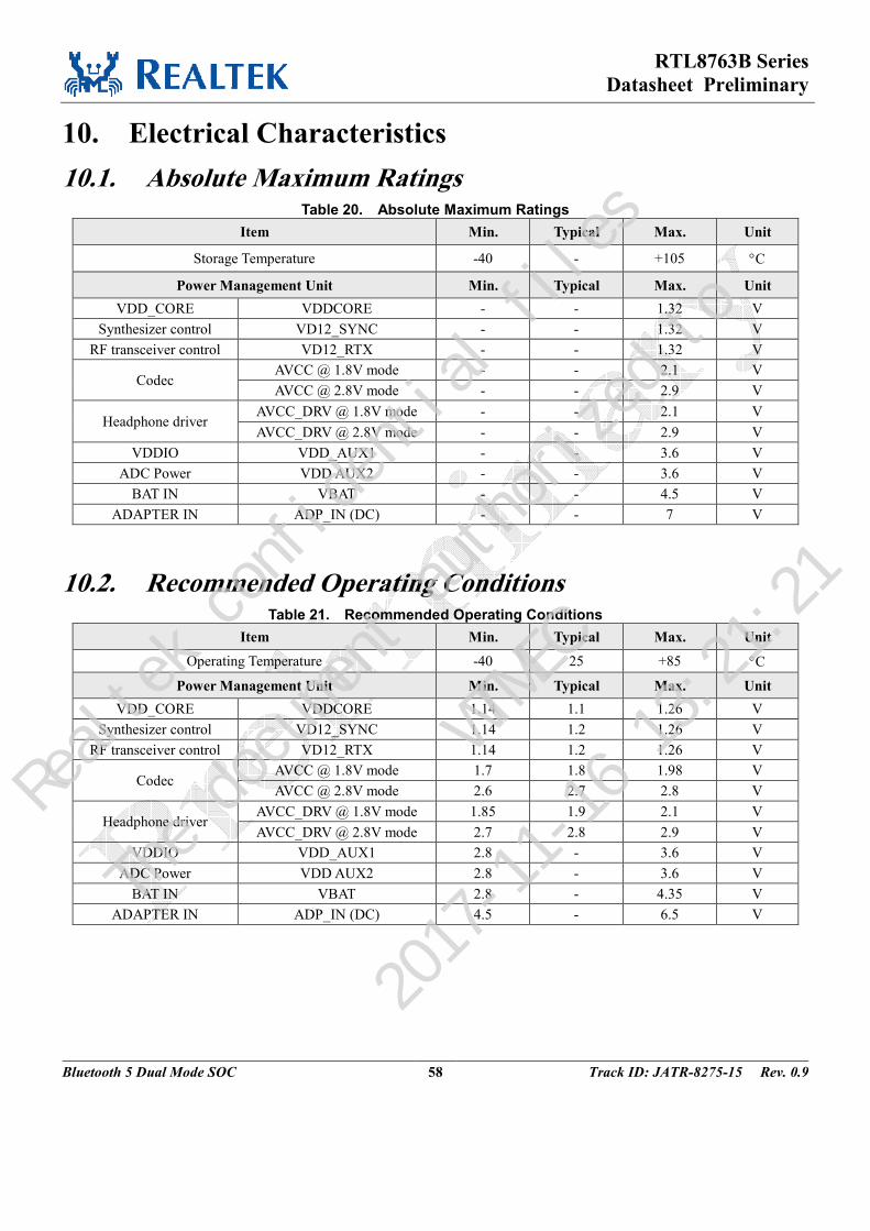
RTL8763B Series
Datasheet Preliminary
Bluetooth 5 Dual Mode SOC 58 Track ID: JATR-8275-15 Rev. 0.9
10. Electrical Characteristics
10.1. Absolute Maximum Ratings Table 20. Absolute Maximum Ratings
Item Min. Typical Max. Unit
Storage Temperature -40 - +105 °C
Power Management Unit Min. Typical Max. Unit
VDD_CORE VDDCORE - - 1.32 V
Synthesizer control VD12_SYNC - - 1.32 V
RF transceiver control VD12_RTX - - 1.32 V
Codec AVCC @ 1.8V mode - - 2.1 V
AVCC @ 2.8V mode - - 2.9 V
Headphone driver AVCC_DRV @ 1.8V mode - - 2.1 V
AVCC_DRV @ 2.8V mode - - 2.9 V
VDDIO VDD_AUX1 - - 3.6 V
ADC Power VDD AUX2 - - 3.6 V
BAT IN VBAT - - 4.5 V
ADAPTER IN ADP_IN (DC) - - 7 V
10.2. Recommended Operating Conditions Table 21. Recommended Operating Conditions
Item Min. Typical Max. Unit
Operating Temperature -40 25 +85 °C
Power Management Unit Min. Typical Max. Unit
VDD_CORE VDDCORE 1.14 1.1 1.26 V
Synthesizer control VD12_SYNC 1.14 1.2 1.26 V
RF transceiver control VD12_RTX 1.14 1.2 1.26 V
Codec AVCC @ 1.8V mode 1.7 1.8 1.98 V
AVCC @ 2.8V mode 2.6 2.7 2.8 V
Headphone driver AVCC_DRV @ 1.8V mode 1.85 1.9 2.1 V
AVCC_DRV @ 2.8V mode 2.7 2.8 2.9 V
VDDIO VDD_AUX1 2.8 - 3.6 V
ADC Power VDD AUX2 2.8 - 3.6 V
BAT IN VBAT 2.8 - 4.35 V
ADAPTER IN ADP_IN (DC) 4.5 - 6.5 V
Realtek confidential files
The document authorized to
WTMEC
2017-11-16 13:21:21
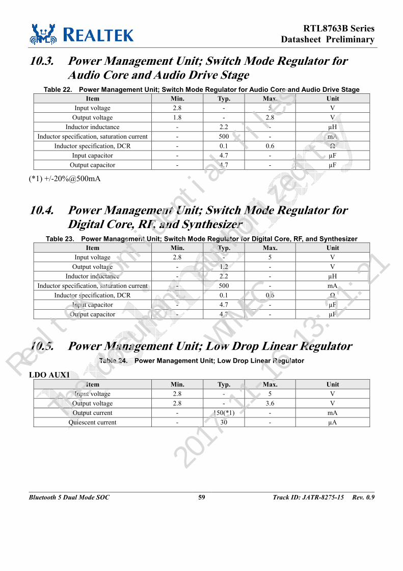
RTL8763B Series
Datasheet Preliminary
Bluetooth 5 Dual Mode SOC 59 Track ID: JATR-8275-15 Rev. 0.9
10.3. Power Management Unit; Switch Mode Regulator for Audio Core and Audio Drive Stage
Table 22. Power Management Unit; Switch Mode Regulator for Audio Core and Audio Drive Stage
Item Min. Typ. Max. Unit
Input voltage 2.8 - 5 V
Output voltage 1.8 - 2.8 V
Inductor inductance - 2.2 - µH
Inductor specification, saturation current - 500 - mA
Inductor specification, DCR - 0.1 0.6 Ω
Input capacitor - 4.7 - µF
Output capacitor - 4.7 - µF
(*1) +/-20%@500mA
10.4. Power Management Unit; Switch Mode Regulator for Digital Core, RF, and Synthesizer
Table 23. Power Management Unit; Switch Mode Regulator for Digital Core, RF, and Synthesizer
Item Min. Typ. Max. Unit
Input voltage 2.8 - 5 V
Output voltage - 1.2 - V
Inductor inductance - 2.2 - µH
Inductor specification, saturation current - 500 - mA
Inductor specification, DCR - 0.1 0.6 Ω
Input capacitor - 4.7 - µF
Output capacitor - 4.7 - µF
10.5. Power Management Unit; Low Drop Linear Regulator Table 24. Power Management Unit; Low Drop Linear Regulator
LDO AUX1
Item Min. Typ. Max. Unit
Input voltage 2.8 - 5 V
Output voltage 2.8 - 3.6 V
Output current - 150(*1) - mA
Quiescent current - 30 - µA
Realtek confidential files
The document authorized to
WTMEC
2017-11-16 13:21:21
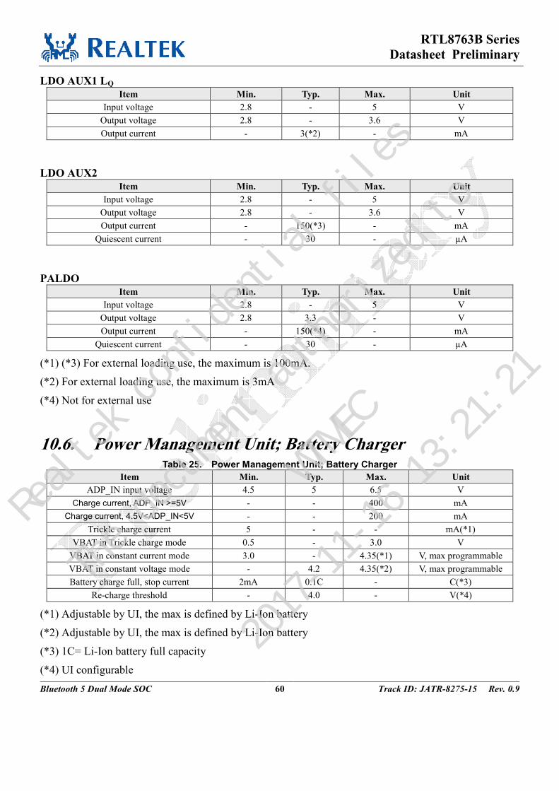
RTL8763B Series
Datasheet Preliminary
Bluetooth 5 Dual Mode SOC 60 Track ID: JATR-8275-15 Rev. 0.9
LDO AUX1 LQ
Item Min. Typ. Max. Unit
Input voltage 2.8 - 5 V
Output voltage 2.8 - 3.6 V
Output current - 3(*2) - mA
LDO AUX2
Item Min. Typ. Max. Unit
Input voltage 2.8 - 5 V
Output voltage 2.8 - 3.6 V
Output current - 150(*3) - mA
Quiescent current - 30 - µA
PALDO
Item Min. Typ. Max. Unit
Input voltage 2.8 - 5 V
Output voltage 2.8 3.3 - V
Output current - 150(*4) - mA
Quiescent current - 30 - µA
(*1) (*3) For external loading use, the maximum is 100mA.
(*2) For external loading use, the maximum is 3mA
(*4) Not for external use
10.6. Power Management Unit; Battery Charger Table 25. Power Management Unit; Battery Charger
Item Min. Typ. Max. Unit
ADP_IN input voltage 4.5 5 6.5 V
Charge current, ADP_IN >=5V - - 400 mA
Charge current, 4.5V<ADP_IN<5V - - 200 mA
Trickle charge current 5 - - mA(*1)
VBAT in Trickle charge mode 0.5 - 3.0 V
VBAT in constant current mode 3.0 - 4.35(*1) V, max programmable
VBAT in constant voltage mode - 4.2 4.35(*2) V, max programmable
Battery charge full, stop current 2mA 0.1C - C(*3)
Re-charge threshold - 4.0 - V(*4)
(*1) Adjustable by UI, the max is defined by Li-Ion battery
(*2) Adjustable by UI, the max is defined by Li-Ion battery
(*3) 1C= Li-Ion battery full capacity
(*4) UI configurable
Realtek confidential files
The document authorized to
WTMEC
2017-11-16 13:21:21
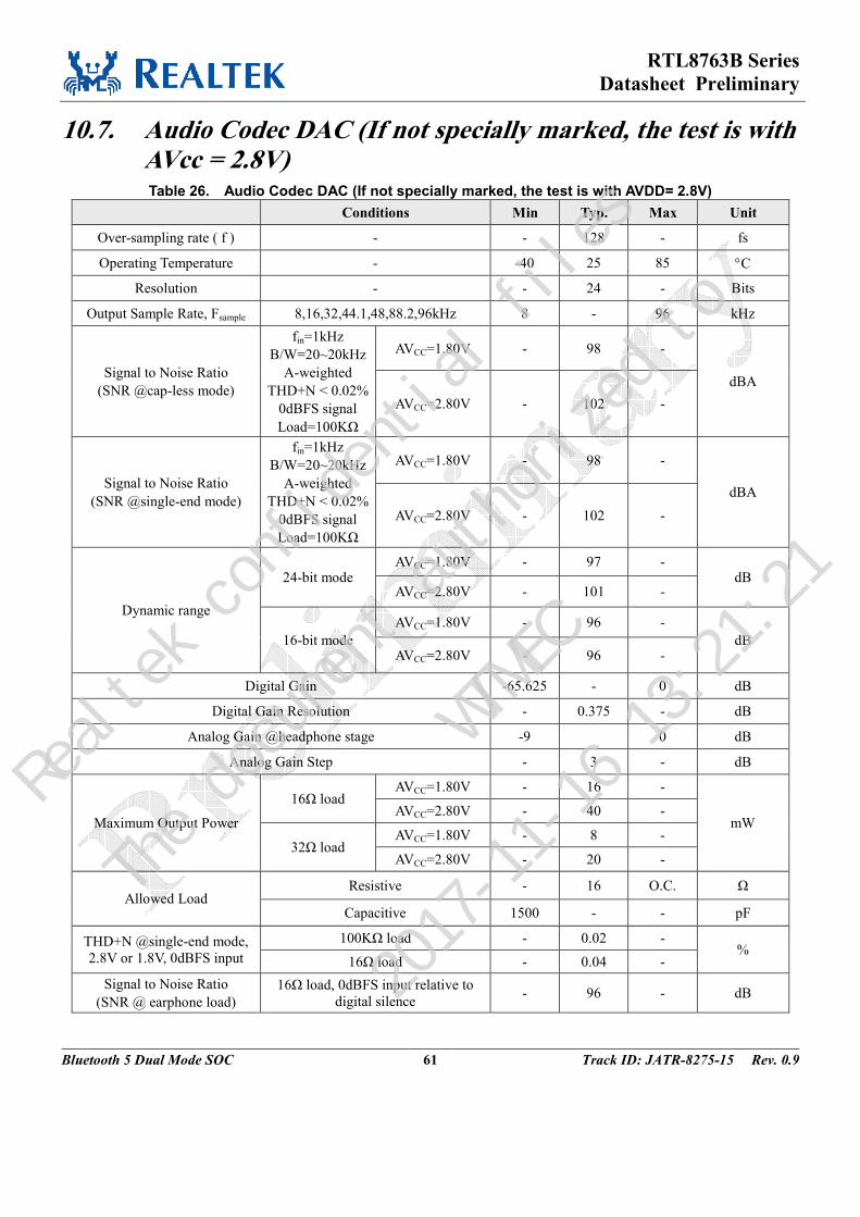
RTL8763B Series
Datasheet Preliminary
Bluetooth 5 Dual Mode SOC 61 Track ID: JATR-8275-15 Rev. 0.9
10.7. Audio Codec DAC (If not specially marked, the test is with AVcc = 2.8V) Table 26. Audio Codec DAC (If not specially marked, the test is with AVDD= 2.8V)
Conditions Min Typ. Max Unit
Over-sampling rate ( f ) - - 128 - fs
Operating Temperature - -40 25 85 °C
Resolution - - 24 - Bits
Output Sample Rate, Fsample 8,16,32,44.1,48,88.2,96kHz 8 - 96 kHz
Signal to Noise Ratio
(SNR @cap-less mode)
fin=1kHz
B/W=20~20kHz
A-weighted
THD+N < 0.02%
0dBFS signal
Load=100KΩ
AVCC=1.80V - 98 -
dBA
AVCC=2.80V - 102 -
Signal to Noise Ratio
(SNR @single-end mode)
fin=1kHz
B/W=20~20kHz
A-weighted
THD+N < 0.02%
0dBFS signal
Load=100KΩ
AVCC=1.80V - 98 -
dBA
AVCC=2.80V - 102 -
Dynamic range
24-bit mode AVCC=1.80V - 97 -
dB AVCC=2.80V - 101 -
16-bit mode
AVCC=1.80V - 96 -
dB AVCC=2.80V - 96 -
Digital Gain -65.625 - 0 dB
Digital Gain Resolution - 0.375 - dB
Analog Gain @headphone stage -9 0 dB
Analog Gain Step - 3 - dB
Maximum Output Power
16Ω load AVCC=1.80V - 16 -
mW AVCC=2.80V - 40 -
32Ω load AVCC=1.80V - 8 -
AVCC=2.80V - 20 -
Allowed Load Resistive - 16 O.C. Ω
Capacitive 1500 - - pF
THD+N @single-end mode,
2.8V or 1.8V, 0dBFS input
100KΩ load - 0.02 - %
16Ω load - 0.04 -
Signal to Noise Ratio
(SNR @ earphone load)
16Ω load, 0dBFS input relative to
digital silence - 96 - dB
Realtek confidential files
The document authorized to
WTMEC
2017-11-16 13:21:21
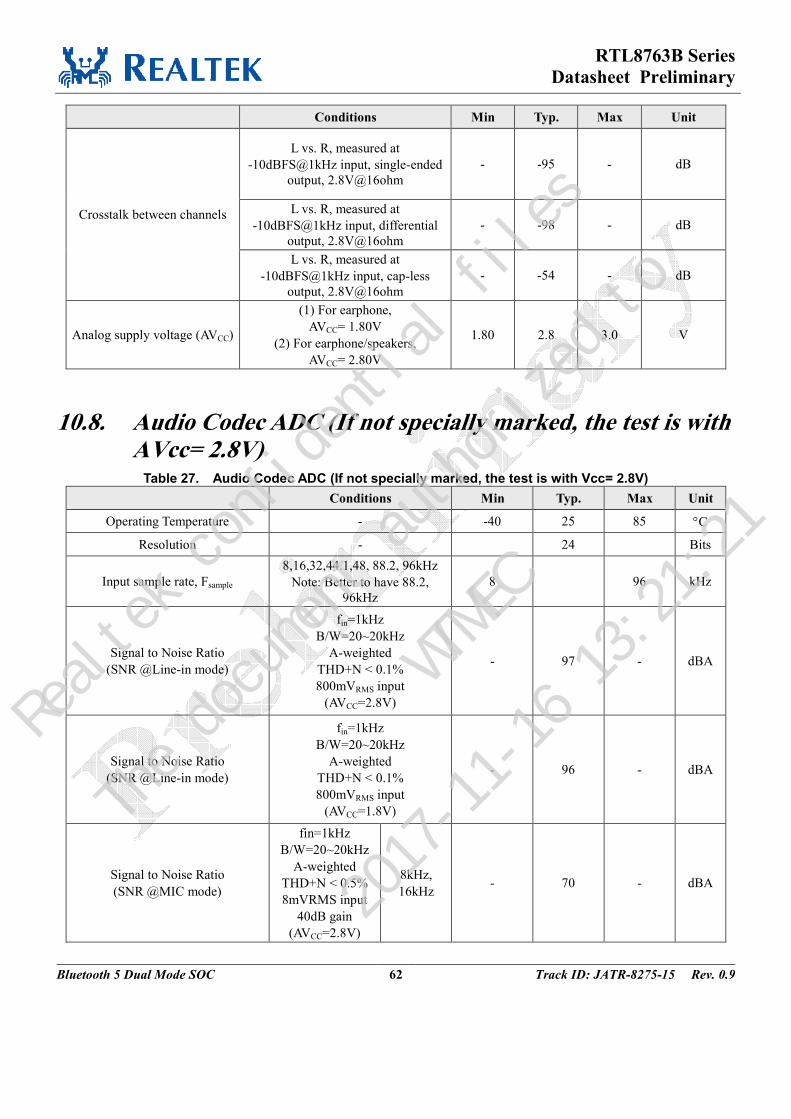
RTL8763B Series
Datasheet Preliminary
Bluetooth 5 Dual Mode SOC 62 Track ID: JATR-8275-15 Rev. 0.9
Conditions Min Typ. Max Unit
Crosstalk between channels
L vs. R, measured at
-10dBFS@1kHz input, single-ended
output, 2.8V@16ohm
- -95 - dB
L vs. R, measured at
-10dBFS@1kHz input, differential
output, 2.8V@16ohm
- -98 - dB
L vs. R, measured at
-10dBFS@1kHz input, cap-less
output, 2.8V@16ohm
- -54 - dB
Analog supply voltage (AVCC)
(1) For earphone,
AVCC= 1.80V
(2) For earphone/speakers,
AVCC= 2.80V
1.80 2.8 3.0 V
10.8. Audio Codec ADC (If not specially marked, the test is with AVcc= 2.8V)
Table 27. Audio Codec ADC (If not specially marked, the test is with Vcc= 2.8V)
Conditions Min Typ. Max Unit
Operating Temperature - -40 25 85 °C
Resolution - 24 Bits
Input sample rate, Fsample
8,16,32,44.1,48, 88.2, 96kHz
Note: Better to have 88.2,
96kHz
8 96 kHz
Signal to Noise Ratio
(SNR @Line-in mode)
fin=1kHz
B/W=20~20kHz
A-weighted
THD+N < 0.1%
800mVRMS input
(AVCC=2.8V)
- 97 - dBA
Signal to Noise Ratio
(SNR @Line-in mode)
fin=1kHz
B/W=20~20kHz
A-weighted
THD+N < 0.1%
800mVRMS input
(AVCC=1.8V)
- 96 - dBA
Signal to Noise Ratio
(SNR @MIC mode)
fin=1kHz
B/W=20~20kHz
A-weighted
THD+N < 0.5%
8mVRMS input
40dB gain
(AVCC=2.8V)
8kHz,
16kHz - 70 - dBA
Realtek confidential files
The document authorized to
WTMEC
2017-11-16 13:21:21
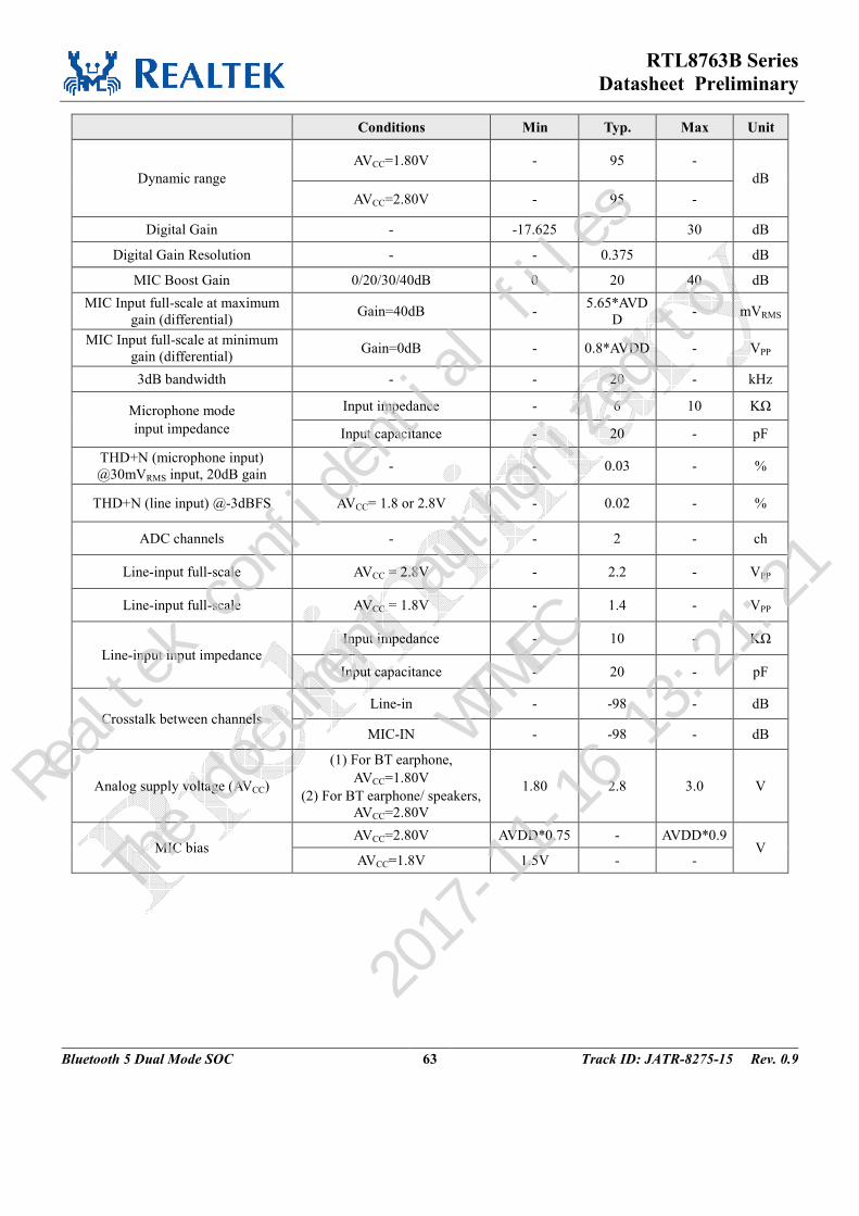
RTL8763B Series
Datasheet Preliminary
Bluetooth 5 Dual Mode SOC 63 Track ID: JATR-8275-15 Rev. 0.9
Conditions Min Typ. Max Unit
Dynamic range
AVCC=1.80V - 95 -
dB
AVCC=2.80V - 95 -
Digital Gain - -17.625 30 dB
Digital Gain Resolution - - 0.375 dB
MIC Boost Gain 0/20/30/40dB 0 20 40 dB
MIC Input full-scale at maximum
gain (differential) Gain=40dB -
5.65*AVD
D - mVRMS
MIC Input full-scale at minimum
gain (differential) Gain=0dB - 0.8*AVDD - VPP
3dB bandwidth - - 20 - kHz
Microphone mode
input impedance
Input impedance - 6 10 KΩ
Input capacitance - 20 - pF
THD+N (microphone input)
@30mVRMS input, 20dB gain - - 0.03 - %
THD+N (line input) @-3dBFS AVCC= 1.8 or 2.8V - 0.02 - %
ADC channels - - 2 - ch
Line-input full-scale AVCC = 2.8V - 2.2 - VPP
Line-input full-scale AVCC = 1.8V - 1.4 - VPP
Line-input input impedance
Input impedance - 10 - KΩ
Input capacitance - 20 - pF
Crosstalk between channels Line-in - -98 - dB
MIC-IN - -98 - dB
Analog supply voltage (AVCC)
(1) For BT earphone,
AVCC=1.80V
(2) For BT earphone/ speakers,
AVCC=2.80V
1.80 2.8 3.0 V
MIC bias AVCC=2.80V AVDD*0.75 - AVDD*0.9
V AVCC=1.8V 1.5V - -
Realtek confidential files
The document authorized to
WTMEC
2017-11-16 13:21:21
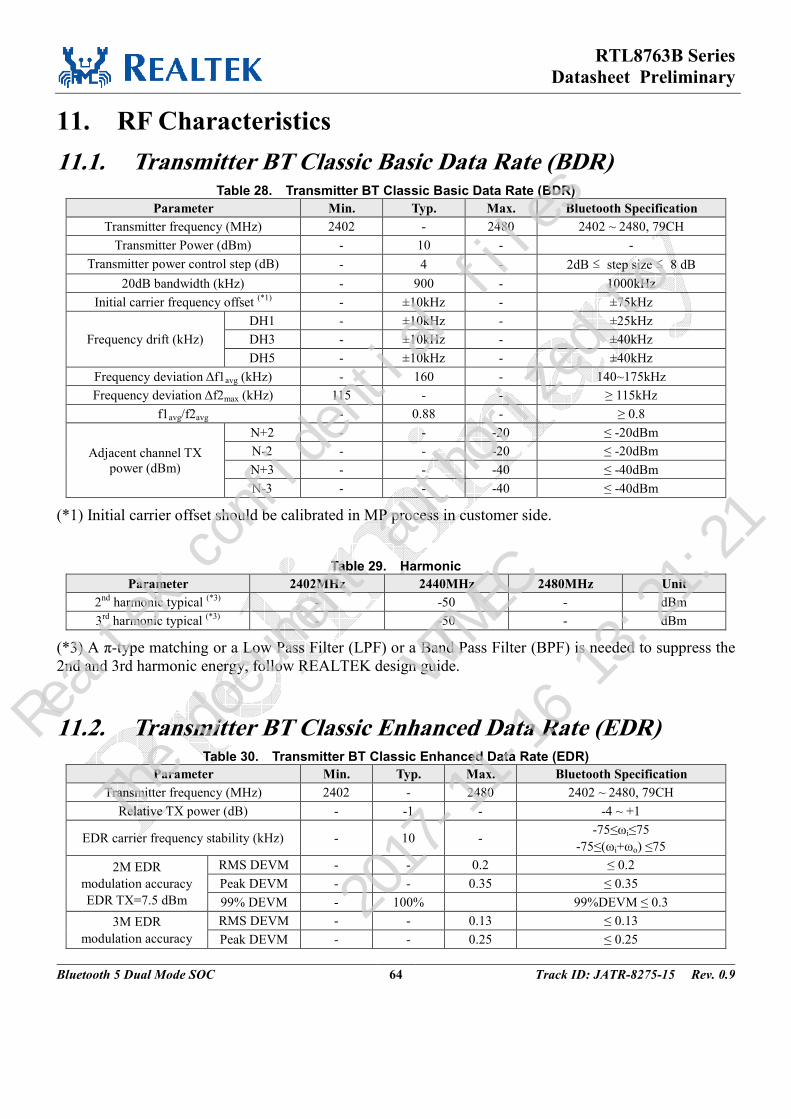
RTL8763B Series
Datasheet Preliminary
Bluetooth 5 Dual Mode SOC 64 Track ID: JATR-8275-15 Rev. 0.9
11. RF Characteristics
11.1. Transmitter BT Classic Basic Data Rate (BDR) Table 28. Transmitter BT Classic Basic Data Rate (BDR)
Parameter Min. Typ. Max. Bluetooth Specification
Transmitter frequency (MHz) 2402 - 2480 2402 ~ 2480, 79CH
Transmitter Power (dBm) - 10 - -
Transmitter power control step (dB) - 4 - 2dB ≤ step size ≤ 8 dB
20dB bandwidth (kHz) - 900 - 1000kHz
Initial carrier frequency offset (*1)
- ±10kHz - ±75kHz
Frequency drift (kHz)
DH1 - ±10kHz - ±25kHz
DH3 - ±10kHz - ±40kHz
DH5 - ±10kHz - ±40kHz
Frequency deviation ∆f1avg (kHz) - 160 - 140~175kHz
Frequency deviation ∆f2max (kHz) 115 - - ≥ 115kHz
f1avg/f2avg - 0.88 - ≥ 0.8
Adjacent channel TX
power (dBm)
N+2 - - -20 ≤ -20dBm
N-2 - - -20 ≤ -20dBm
N+3 - - -40 ≤ -40dBm
N-3 - - -40 ≤ -40dBm
(*1) Initial carrier offset should be calibrated in MP process in customer side.
Table 29. Harmonic
Parameter 2402MHz 2440MHz 2480MHz Unit
2nd
harmonic typical (*3)
- -50 - dBm
3rd
harmonic typical (*3)
- -50 - dBm
(*3) A π-type matching or a Low Pass Filter (LPF) or a Band Pass Filter (BPF) is needed to suppress the
2nd and 3rd harmonic energy, follow REALTEK design guide.
11.2. Transmitter BT Classic Enhanced Data Rate (EDR) Table 30. Transmitter BT Classic Enhanced Data Rate (EDR)
Parameter Min. Typ. Max. Bluetooth Specification
Transmitter frequency (MHz) 2402 - 2480 2402 ~ 2480, 79CH
Relative TX power (dB) - -1 - -4 ~ +1
EDR carrier frequency stability (kHz) - 10 - -75≤ωi≤75
-75≤(ωi+ωo) ≤75
2M EDR
modulation accuracy
EDR TX=7.5 dBm
RMS DEVM - - 0.2 ≤ 0.2
Peak DEVM - - 0.35 ≤ 0.35
99% DEVM - 100% 99%DEVM ≤ 0.3
3M EDR
modulation accuracy
RMS DEVM - - 0.13 ≤ 0.13
Peak DEVM - - 0.25 ≤ 0.25
Realtek confidential files
The document authorized to
WTMEC
2017-11-16 13:21:21
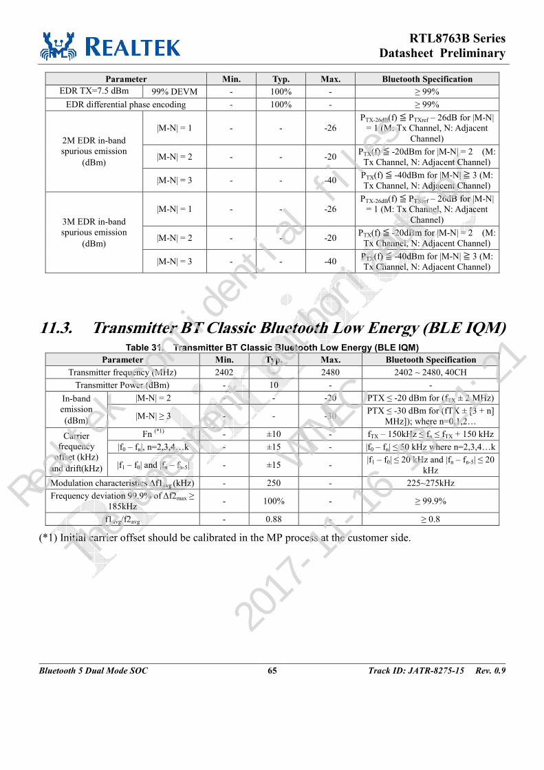
RTL8763B Series
Datasheet Preliminary
Bluetooth 5 Dual Mode SOC 65 Track ID: JATR-8275-15 Rev. 0.9
Parameter Min. Typ. Max. Bluetooth Specification
EDR TX=7.5 dBm 99% DEVM - 100% - ≥ 99%
EDR differential phase encoding - 100% - ≥ 99%
2M EDR in-band
spurious emission
(dBm)
|M-N| = 1 - - -26
PTX-26dB(f) ≦ PTXref – 26dB for |M-N|
= 1 (M: Tx Channel, N: Adjacent
Channel)
|M-N| = 2 - - -20 PTX(f) ≦ -20dBm for |M-N| = 2 (M:
Tx Channel, N: Adjacent Channel)
|M-N| = 3 - - -40 PTX(f) ≦ -40dBm for |M-N| ≧ 3 (M:
Tx Channel, N: Adjacent Channel)
3M EDR in-band
spurious emission
(dBm)
|M-N| = 1 - - -26 PTX-26dB(f) ≦ PTXref – 26dB for |M-N|
= 1 (M: Tx Channel, N: Adjacent
Channel)
|M-N| = 2 - - -20 PTX(f) ≦ -20dBm for |M-N| = 2 (M:
Tx Channel, N: Adjacent Channel)
|M-N| = 3 - - -40 PTX(f) ≦ -40dBm for |M-N| ≧ 3 (M:
Tx Channel, N: Adjacent Channel)
11.3. Transmitter BT Classic Bluetooth Low Energy (BLE IQM) Table 31. Transmitter BT Classic Bluetooth Low Energy (BLE IQM)
Parameter Min. Typ. Max. Bluetooth Specification
Transmitter frequency (MHz) 2402 - 2480 2402 ~ 2480, 40CH
Transmitter Power (dBm) - 10 - -
In-band
emission
(dBm)
|M-N| = 2 - - -20 PTX ≤ -20 dBm for (fTX ± 2 MHz)
|M-N| ≥ 3 - - -30 PTX ≤ -30 dBm for (fTX ± [3 + n]
MHz]); where n=0,1,2…
Carrier
frequency
offset (kHz)
and drift(kHz)
Fn (*1)
- ±10 - fTX – 150kHz ≤ fn ≤ fTX + 150 kHz
|f0 – fn|, n=2,3,4…k - ±15 - |f0 – fn| ≤ 50 kHz where n=2,3,4…k
|f1 – f0| and |fn – fn-5| - ±15 - |f1 – f0| ≤ 20 kHz and |fn – fn-5| ≤ 20
kHz
Modulation characteristics ∆f1avg (kHz) - 250 - 225~275kHz
Frequency deviation 99.9% of ∆f2max ≥
185kHz - 100% - ≥ 99.9%
f1avg/f2avg - 0.88 - ≥ 0.8
(*1) Initial carrier offset should be calibrated in the MP process at the customer side.
Realtek confidential files
The document authorized to
WTMEC
2017-11-16 13:21:21
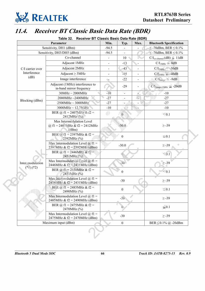
RTL8763B Series
Datasheet Preliminary
Bluetooth 5 Dual Mode SOC 66 Track ID: JATR-8275-15 Rev. 0.9
11.4. Receiver BT Classic Basic Data Rate (BDR) Table 32. Receiver BT Classic Basic Data Rate (BDR)
Parameter Min. Typ. Max. Bluetooth Specification
Sensitivity, DH1 (dBm) -94.5 - - ≤ -70dBm, BER ≤ 0.1%
Sensitivity, DH3/DH5 (dBm) -94.5 - - ≤ -70dBm, BER ≤ 0.1%
C/I carrier over
Interference
(dB)
Co-channel - 10 - C/Ico-channel (dB) ≦ 11dB
Adjacent 1MHz - -13 - C/I1MHz ≦ 0dB
Adjacent 2MHz - -43 - C/I2MHz ≦ -30dB
Adjacent ≥ 3MHz - -45 - C/I3MHz ≦ -40dB
Image interference - -22 - C/IImage ≦ -9dB
Adjacent (1MHz) interference to
in-band mirror frequency - -29 - C/IImage±1MHz ≦ -20dB
Blocking (dBm)
30MHz ~ 2000MHz -10 - - -10
2000MHz ~2400MHz -27 - - -27
2500MHz ~ 3000MHz -27 - - -27
3000MHz ~ 12.75GHz -10 - - -10
Inter-modulation
(*1) (*2)
BER @ f1 = 2407MHz & f2 =
2412MHz (%) 0 ≦0.1
Max Intermodulation Level
@ f1 = 2407MHz & f2 = 2412MHz
(dBm)
-30.0 ≥ -39
BER @ f1 = 2397MHz & f2 =
2392MHz (%) 0 ≦0.1
Max Intermodulation Level @ f1 =
2397MHz & f2 = 2392MHz (dBm) -30.0 ≥ -39
BER @ f1 = 2446MHz & f2 =
2451MHz (%) 0 ≦0.1
Max Intermodulation Level @ f1 =
2446MHz & f2 = 2451MHz (dBm) -30 ≥ -39
BER @ f1 = 2436MHz & f2 =
2431MHz (%) 0 ≦0.1
Max Intermodulation Level @ f1 =
2436MHz & f2 = 2431MHz (dBm) -30 ≥ -39
BER @ f1 = 2485MHz & f2 =
2490MHz (%) 0 ≦0.1
Max Intermodulation Level @ f1 =
2485MHz & f2 = 2490MHz (dBm) -30 ≥ -39
BER @ f1 = 2475MHz & f2 =
2470MHz (%) 0 ≦0.1
Max Intermodulation Level @ f1 =
2475MHz & f2 = 2470MHz (dBm) -30 ≥ -39
Maximum input (dBm) 0 BER≦0.1% @ -20dBm
Realtek confidential files
The document authorized to
WTMEC
2017-11-16 13:21:21
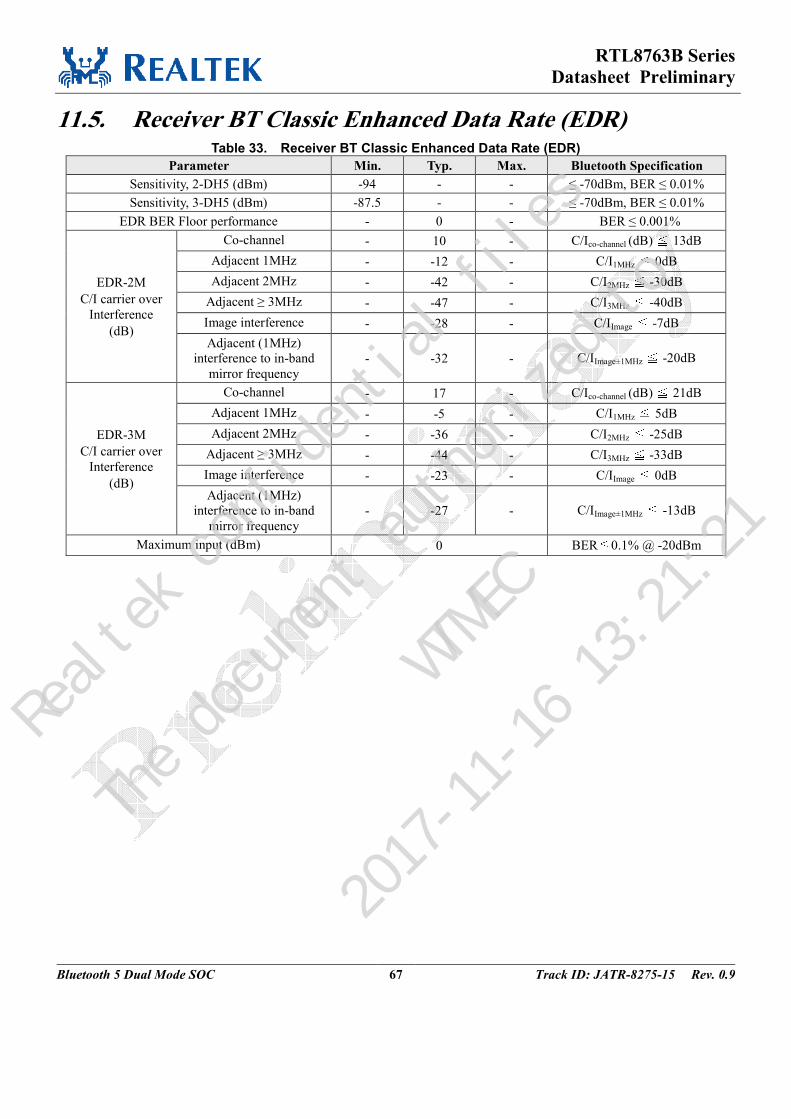
RTL8763B Series
Datasheet Preliminary
Bluetooth 5 Dual Mode SOC 67 Track ID: JATR-8275-15 Rev. 0.9
11.5. Receiver BT Classic Enhanced Data Rate (EDR) Table 33. Receiver BT Classic Enhanced Data Rate (EDR)
Parameter Min. Typ. Max. Bluetooth Specification
Sensitivity, 2-DH5 (dBm) -94 - - ≤ -70dBm, BER ≤ 0.01%
Sensitivity, 3-DH5 (dBm) -87.5 - - ≤ -70dBm, BER ≤ 0.01%
EDR BER Floor performance - 0 - BER ≤ 0.001%
EDR-2M
C/I carrier over
Interference
(dB)
Co-channel - 10 - C/Ico-channel (dB) ≦ 13dB
Adjacent 1MHz - -12 - C/I1MHz ≦ 0dB
Adjacent 2MHz - -42 - C/I2MHz ≦ -30dB
Adjacent ≥ 3MHz - -47 - C/I3MHz ≦ -40dB
Image interference - -28 - C/IImage ≦ -7dB
Adjacent (1MHz)
interference to in-band
mirror frequency
- -32 - C/IImage±1MHz ≦ -20dB
EDR-3M
C/I carrier over
Interference
(dB)
Co-channel - 17 - C/Ico-channel (dB) ≦ 21dB
Adjacent 1MHz - -5 - C/I1MHz ≦ 5dB
Adjacent 2MHz - -36 - C/I2MHz ≦ -25dB
Adjacent ≥ 3MHz - -44 - C/I3MHz ≦ -33dB
Image interference - -23 - C/IImage ≦ 0dB
Adjacent (1MHz)
interference to in-band
mirror frequency
- -27 - C/IImage±1MHz ≦ -13dB
Maximum input (dBm) 0 BER≦0.1% @ -20dBm
Realtek confidential files
The document authorized to
WTMEC
2017-11-16 13:21:21
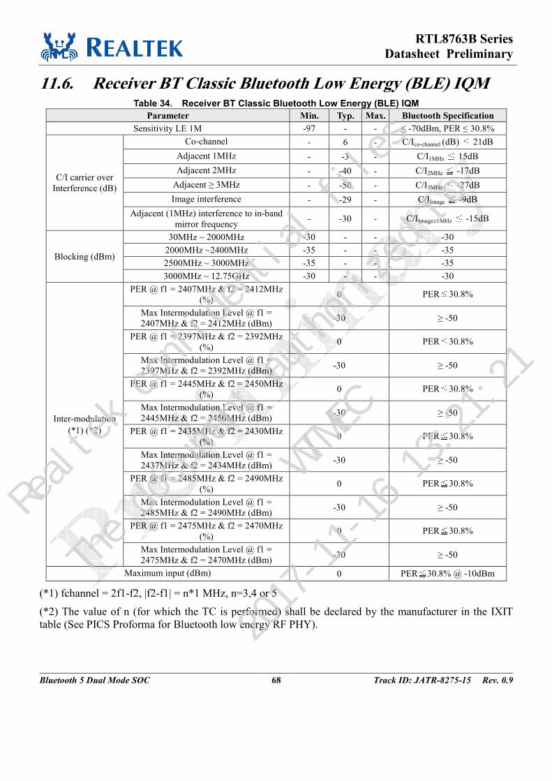
RTL8763B Series
Datasheet Preliminary
Bluetooth 5 Dual Mode SOC 68 Track ID: JATR-8275-15 Rev. 0.9
11.6. Receiver BT Classic Bluetooth Low Energy (BLE) IQM Table 34. Receiver BT Classic Bluetooth Low Energy (BLE) IQM
Parameter Min. Typ. Max. Bluetooth Specification
Sensitivity LE 1M -97 - - ≤ -70dBm, PER ≤ 30.8%
C/I carrier over
Interference (dB)
Co-channel - 6 - C/Ico-channel (dB) ≦ 21dB
Adjacent 1MHz - -3 - C/I1MHz ≦ 15dB
Adjacent 2MHz - -40 - C/I2MHz ≦ -17dB
Adjacent ≥ 3MHz - -50 - C/I3MHz ≦ -27dB
Image interference - -29 - C/IImage ≦ -9dB
Adjacent (1MHz) interference to in-band
mirror frequency - -30 - C/IImage±1MHz ≦ -15dB
Blocking (dBm)
30MHz ~ 2000MHz -30 - - -30
2000MHz ~2400MHz -35 - - -35
2500MHz ~ 3000MHz -35 - - -35
3000MHz ~ 12.75GHz -30 - - -30
Inter-modulation
(*1) (*2)
PER @ f1 = 2407MHz & f2 = 2412MHz
(%) 0 PER≦30.8%
Max Intermodulation Level @ f1 =
2407MHz & f2 = 2412MHz (dBm) -30 ≥ -50
PER @ f1 = 2397MHz & f2 = 2392MHz
(%) 0 PER≦30.8%
Max Intermodulation Level @ f1 =
2397MHz & f2 = 2392MHz (dBm) -30 ≥ -50
PER @ f1 = 2445MHz & f2 = 2450MHz
(%) 0 PER≦30.8%
Max Intermodulation Level @ f1 =
2445MHz & f2 = 2450MHz (dBm) -30 ≥ -50
PER @ f1 = 2435MHz & f2 = 2430MHz
(%) 0 PER≦30.8%
Max Intermodulation Level @ f1 =
2437MHz & f2 = 2434MHz (dBm) -30 ≥ -50
PER @ f1 = 2485MHz & f2 = 2490MHz
(%) 0 PER≦30.8%
Max Intermodulation Level @ f1 =
2485MHz & f2 = 2490MHz (dBm) -30 ≥ -50
PER @ f1 = 2475MHz & f2 = 2470MHz
(%) 0 PER≦30.8%
Max Intermodulation Level @ f1 =
2475MHz & f2 = 2470MHz (dBm) -30 ≥ -50
Maximum input (dBm) 0 PER≦30.8% @ -10dBm
(*1) fchannel = 2f1-f2, |f2-f1| = n*1 MHz, n=3,4 or 5
(*2) The value of n (for which the TC is performed) shall be declared by the manufacturer in the IXIT
table (See PICS Proforma for Bluetooth low energy RF PHY).
Realtek confidential files
The document authorized to
WTMEC
2017-11-16 13:21:21
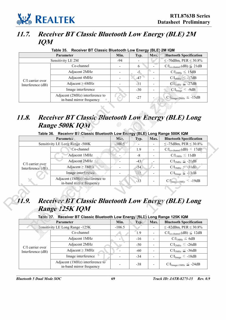
RTL8763B Series
Datasheet Preliminary
Bluetooth 5 Dual Mode SOC 69 Track ID: JATR-8275-15 Rev. 0.9
11.7. Receiver BT Classic Bluetooth Low Energy (BLE) 2M IQM
Table 35. Receiver BT Classic Bluetooth Low Energy (BLE) 2M IQM
Parameter Min. Typ. Max. Bluetooth Specification
Sensitivity LE 2M -94 - - ≤ -70dBm, PER ≤ 30.8%
C/I carrier over
Interference (dB)
Co-channel - 6 - C/Ico-channel (dB) ≦ 21dB
Adjacent 2MHz - -5 - C/I2MHz ≦ 15dB
Adjacent 4MHz - -47 - C/I4MHz ≦ -17dB
Adjacent ≥ 6MHz - -51 - C/I6MHz ≦ -27dB
Image interference - -30 - C/IImage ≦ -9dB
Adjacent (2MHz) interference to
in-band mirror frequency - -27 - C/IImage±2MHz ≦ -15dB
11.8. Receiver BT Classic Bluetooth Low Energy (BLE) Long Range 500K IQM Table 36. Receiver BT Classic Bluetooth Low Energy (BLE) Long Range 500K IQM
Parameter Min. Typ. Max. Bluetooth Specification
Sensitivity LE Long Range -500K -100.5 - - ≤ -75dBm, PER ≤ 30.8%
C/I carrier over
Interference (dB)
Co-channel - 1.9 - C/Ico-channel (dB) ≦ 17dB
Adjacent 1MHz - -8 - C/I1MHz ≦ 11dB
Adjacent 2MHz - -43 - C/I2MHz ≦ -21dB
Adjacent ≥ 3MHz - -54 - C/I3MHz ≦ -31dB
Image interference - -33 - C/IImage ≦ -13dB
Adjacent (1MHz) interference to
in-band mirror frequency - -33 - C/IImage±1MHz ≦ -19dB
11.9. Receiver BT Classic Bluetooth Low Energy (BLE) Long Range 125K IQM Table 37. Receiver BT Classic Bluetooth Low Energy (BLE) Long Range 125K IQM
Parameter Min. Typ. Max. Bluetooth Specification
Sensitivity LE Long Range -125K -106.5 - - ≤ -82dBm, PER ≤ 30.8%
C/I carrier over
Interference (dB)
Co-channel - 1.9 - C/Ico-channel (dB) ≦ 12dB
Adjacent 1MHz - -16 - C/I1MHz ≦ 6dB
Adjacent 2MHz - -50 - C/I2MHz ≦ -26dB
Adjacent ≥ 3MHz - -60 - C/I3MHz ≦ -36dB
Image interference - -34 - C/IImage ≦ -18dB
Adjacent (1MHz) interference to
in-band mirror frequency - -38 - C/IImage±1MHz ≦ -24dB
Realtek confidential files
The document authorized to
WTMEC
2017-11-16 13:21:21
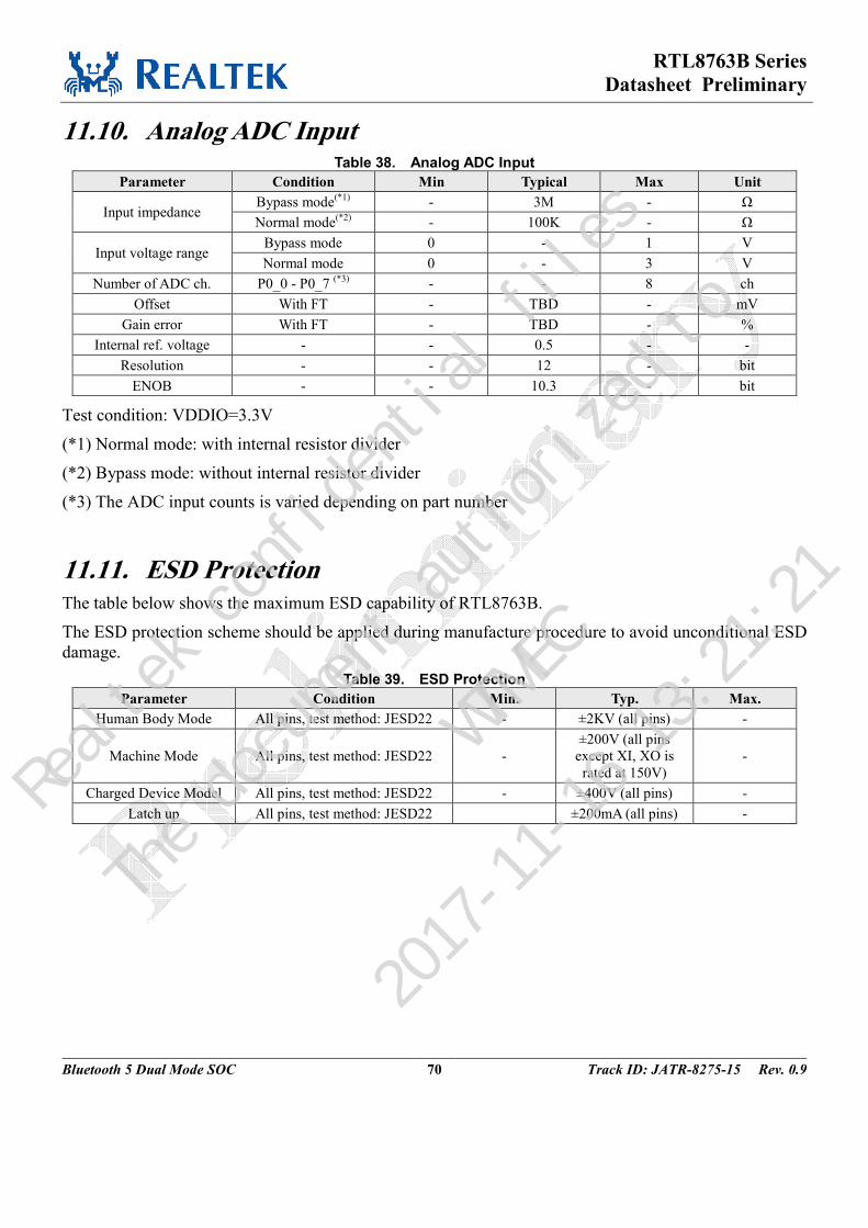
RTL8763B Series
Datasheet Preliminary
Bluetooth 5 Dual Mode SOC 70 Track ID: JATR-8275-15 Rev. 0.9
11.10. Analog ADC Input Table 38. Analog ADC Input
Parameter Condition Min Typical Max Unit
Input impedance Bypass mode
(*1) - 3M - Ω
Normal mode(*2)
- 100K - Ω
Input voltage range Bypass mode 0 - 1 V
Normal mode 0 - 3 V
Number of ADC ch. P0_0 - P0_7 (*3)
- - 8 ch
Offset With FT - TBD - mV
Gain error With FT - TBD - %
Internal ref. voltage - - 0.5 - -
Resolution - - 12 - bit
ENOB - - 10.3 - bit
Test condition: VDDIO=3.3V
(*1) Normal mode: with internal resistor divider
(*2) Bypass mode: without internal resistor divider
(*3) The ADC input counts is varied depending on part number
11.11. ESD Protection The table below shows the maximum ESD capability of RTL8763B.
The ESD protection scheme should be applied during manufacture procedure to avoid unconditional ESD
damage.
Table 39. ESD Protection
Parameter Condition Min. Typ. Max.
Human Body Mode All pins, test method: JESD22 - ±2KV (all pins) -
Machine Mode All pins, test method: JESD22 -
±200V (all pins
except XI, XO is
rated at 150V)
-
Charged Device Model All pins, test method: JESD22 - ±400V (all pins) -
Latch up All pins, test method: JESD22 ±200mA (all pins) -
Realtek confidential files
The document authorized to
WTMEC
2017-11-16 13:21:21
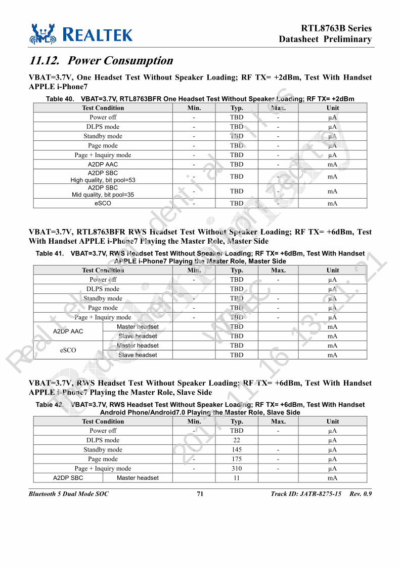
RTL8763B Series
Datasheet Preliminary
Bluetooth 5 Dual Mode SOC 71 Track ID: JATR-8275-15 Rev. 0.9
11.12. Power Consumption
VBAT=3.7V, One Headset Test Without Speaker Loading; RF TX= +2dBm, Test With Handset
APPLE i-Phone7
Table 40. VBAT=3.7V, RTL8763BFR One Headset Test Without Speaker Loading; RF TX= +2dBm
Test Condition Min. Typ. Max. Unit
Power off - TBD - µA
DLPS mode - TBD - µA
Standby mode - TBD - µA
Page mode - TBD - µA
Page + Inquiry mode - TBD - µA
A2DP AAC - TBD - mA
A2DP SBC High quality, bit pool=53
- TBD - mA
A2DP SBC Mid quality, bit pool=35
- TBD - mA
eSCO - TBD - mA
VBAT=3.7V, RTL8763BFR RWS Headset Test Without Speaker Loading; RF TX= +6dBm, Test
With Handset APPLE i-Phone7 Playing the Master Role, Master Side
Table 41. VBAT=3.7V, RWS Headset Test Without Speaker Loading; RF TX= +6dBm, Test With Handset APPLE i-Phone7 Playing the Master Role, Master Side
Test Condition Min. Typ. Max. Unit
Power off - TBD - µA
DLPS mode TBD µA
Standby mode - TBD - µA
Page mode - TBD - µA
Page + Inquiry mode - TBD - µA
A2DP AAC Master headset TBD mA
Slave headset TBD mA
eSCO Master headset TBD mA
Slave headset TBD mA
VBAT=3.7V, RWS Headset Test Without Speaker Loading; RF TX= +6dBm, Test With Handset
APPLE i-Phone7 Playing the Master Role, Slave Side
Table 42. VBAT=3.7V, RWS Headset Test Without Speaker Loading; RF TX= +6dBm, Test With Handset Android Phone/Android7.0 Playing the Master Role, Slave Side
Test Condition Min. Typ. Max. Unit
Power off - TBD - µA
DLPS mode 22 µA
Standby mode - 145 - µA
Page mode - 175 - µA
Page + Inquiry mode - 310 - µA
A2DP SBC Master headset 11 mA
Realtek confidential files
The document authorized to
WTMEC
2017-11-16 13:21:21
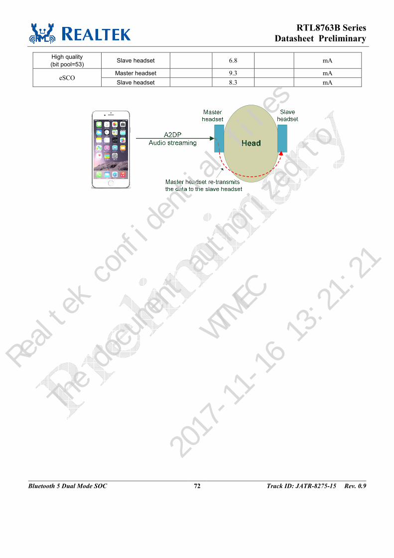
RTL8763B Series
Datasheet Preliminary
Bluetooth 5 Dual Mode SOC 72 Track ID: JATR-8275-15 Rev. 0.9
High quality
(bit pool=53) Slave headset 6.8 mA
eSCO Master headset 9.3 mA
Slave headset 8.3 mA
Realtek confidential files
The document authorized to
WTMEC
2017-11-16 13:21:21
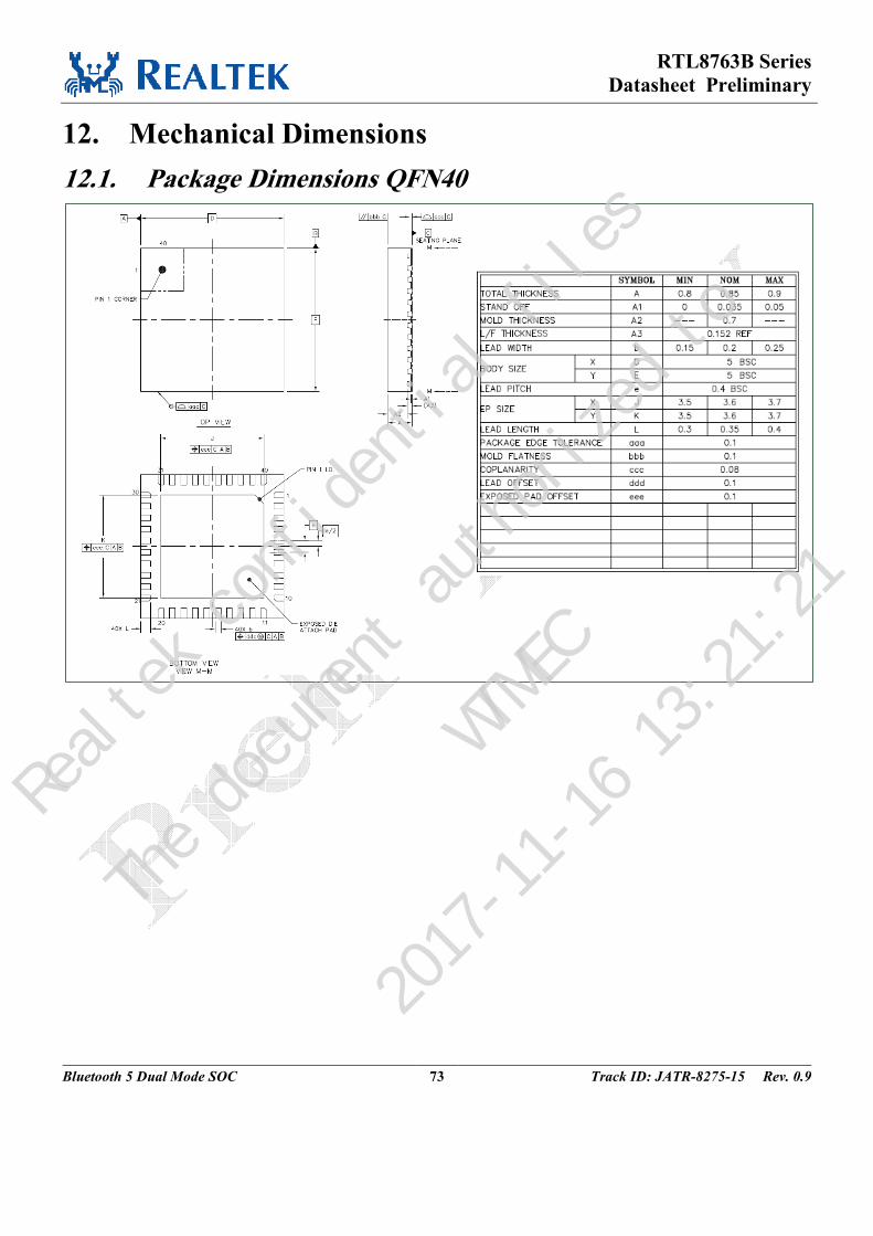
RTL8763B Series
Datasheet Preliminary
Bluetooth 5 Dual Mode SOC 73 Track ID: JATR-8275-15 Rev. 0.9
12. Mechanical Dimensions
12.1. Package Dimensions QFN40
Realtek confidential files
The document authorized to
WTMEC
2017-11-16 13:21:21
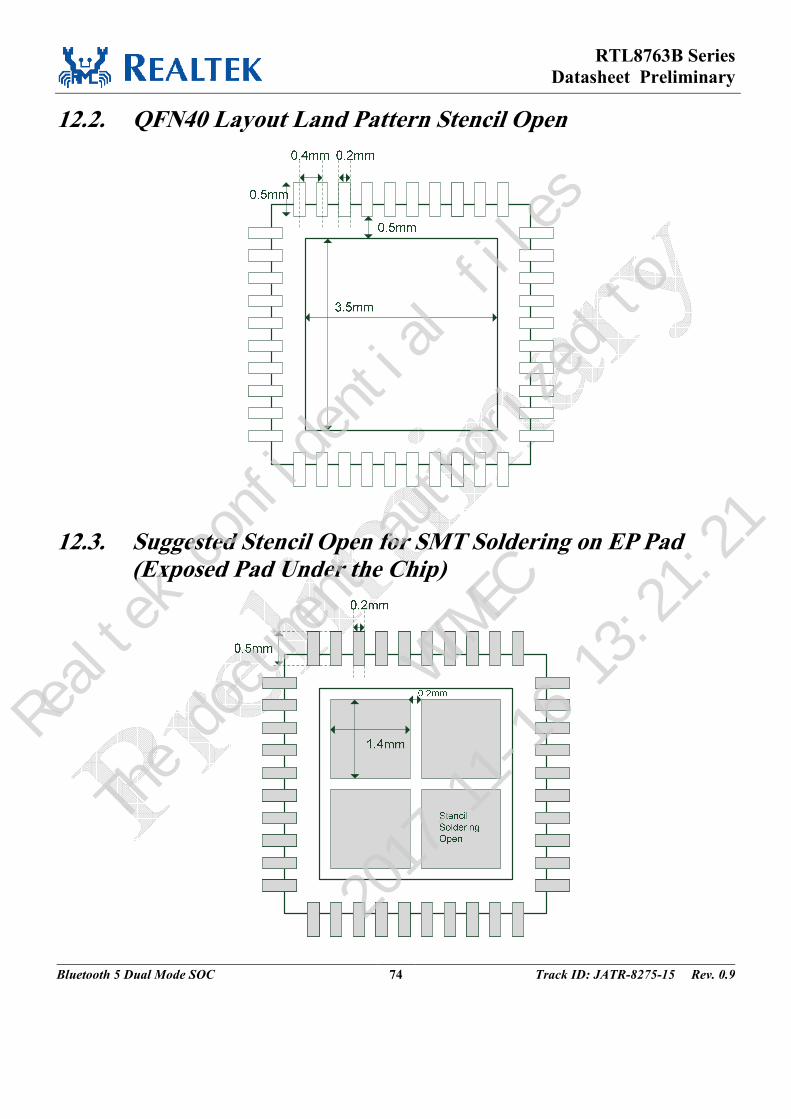
RTL8763B Series
Datasheet Preliminary
Bluetooth 5 Dual Mode SOC 74 Track ID: JATR-8275-15 Rev. 0.9
12.2. QFN40 Layout Land Pattern Stencil Open
12.3. Suggested Stencil Open for SMT Soldering on EP Pad (Exposed Pad Under the Chip)
Realtek confidential files
The document authorized to
WTMEC
2017-11-16 13:21:21
RTL8763B Series
Datasheet Preliminary
Bluetooth 5 Dual Mode SOC 75 Track ID: JATR-8275-15 Rev. 0.9
12.4. Package Dimension QFN48 6x6mm2
12.5. QFN48 Layout Land Pattern Stencil Open
4.0mm
0.2mm
0.2mm
0.4mm
0.4mm
0.6mm
Realtek confidential files
The document authorized to
WTMEC
2017-11-16 13:21:21
RTL8763B Series
Datasheet Preliminary
Bluetooth 5 Dual Mode SOC 76 Track ID: JATR-8275-15 Rev. 0.9
12.6. Suggested Stencil Open for SMT Soldering on EP Pad (Exposed Pad Under the Chip)
9.3mm
0.2mm
0.2mm
0.4mm
0.4mm
0.3mm
Realtek confidential files
The document authorized to
WTMEC
2017-11-16 13:21:21
RTL8763B Series
Datasheet Preliminary
Bluetooth 5 Dual Mode SOC 77 Track ID: JATR-8275-15 Rev. 0.9
12.7. Package Dimension QFN68 8x8mm2
Realtek confidential files
The document authorized to
WTMEC
2017-11-16 13:21:21
RTL8763B Series
Datasheet Preliminary
Bluetooth 5 Dual Mode SOC 78 Track ID: JATR-8275-15 Rev. 0.9
12.8. QFN68 Layout Land Pattern Stencil Open
12.9. Suggested Stencil Open for SMT Soldering on EP Pad (Exposed Pad Under the Chip)
Realtek confidential files
The document authorized to
WTMEC
2017-11-16 13:21:21
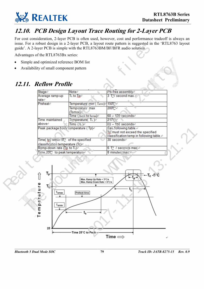
RTL8763B Series
Datasheet Preliminary
Bluetooth 5 Dual Mode SOC 79 Track ID: JATR-8275-15 Rev. 0.9
12.10. PCB Design Layout Trace Routing for 2-Layer PCB For cost consideration, 2-layer PCB is often used, however, cost and performance tradeoff is always an
issue. For a robust design in a 2-layer PCB, a layout route pattern is suggested in the ‘RTL8763 layout
guide’. A 2-layer PCB is simple with the RTL8763BM/BF/BFR audio solution
Advantages of the RTL8763Bx series:
• Simple and optimized reference BOM list
• Availability of small component pattern
12.11. Reflow Profile
Realtek confidential files
The document authorized to
WTMEC
2017-11-16 13:21:21
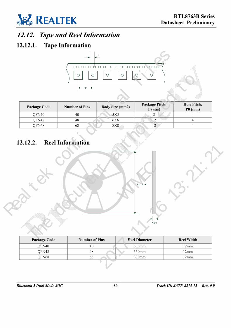
RTL8763B Series
Datasheet Preliminary
Bluetooth 5 Dual Mode SOC 80 Track ID: JATR-8275-15 Rev. 0.9
12.12. Tape and Reel Information
12.12.1. Tape Information
Package Code Number of Pins Body Size (mm2) Package Pitch:
P (mm)
Hole Pitch:
P0 (mm)
QFN40 40 5X5 8 4
QFN48 48 6X6 12 4
QFN68 68 8X8 12 4
12.12.2. Reel Information
Package Code Number of Pins Reel Diameter Reel Width
QFN40 40 330mm 12mm
QFN48 48 330mm 12mm
QFN68 68 330mm 12mm
Realtek confidential files
The document authorized to
WTMEC
2017-11-16 13:21:21
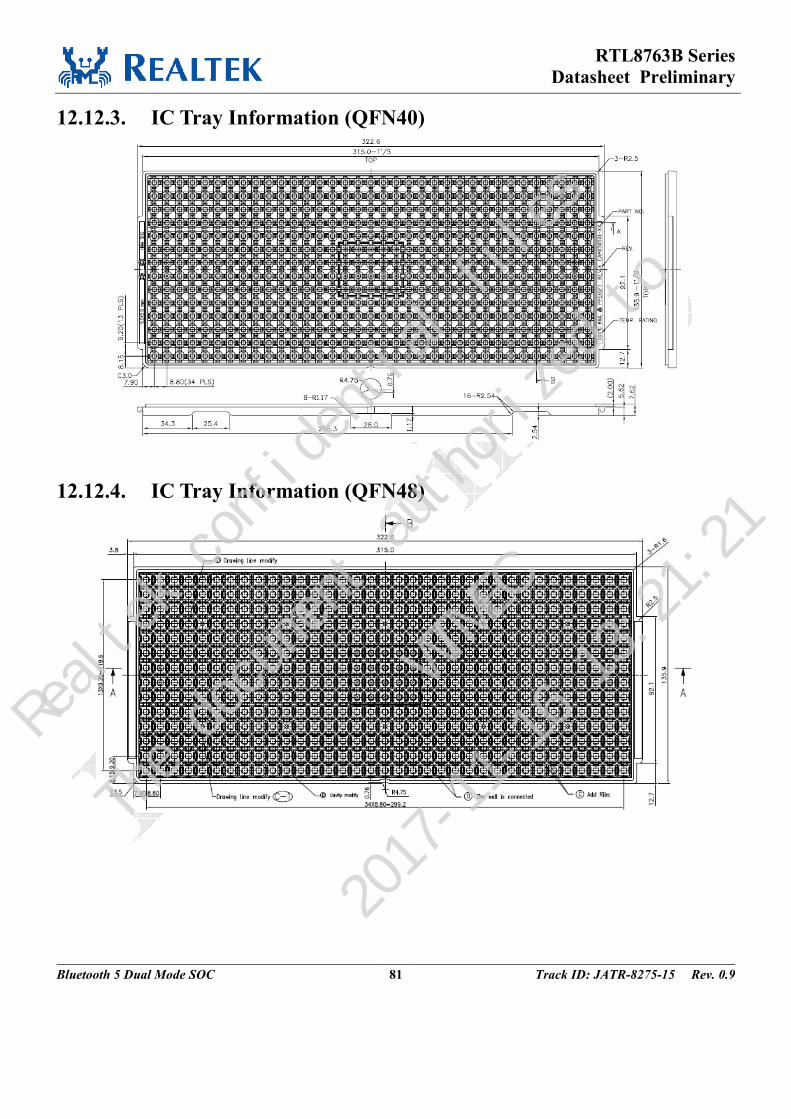
RTL8763B Series
Datasheet Preliminary
Bluetooth 5 Dual Mode SOC 81 Track ID: JATR-8275-15 Rev. 0.9
12.12.3. IC Tray Information (QFN40)
12.12.4. IC Tray Information (QFN48)
Realtek confidential files
The document authorized to
WTMEC
2017-11-16 13:21:21
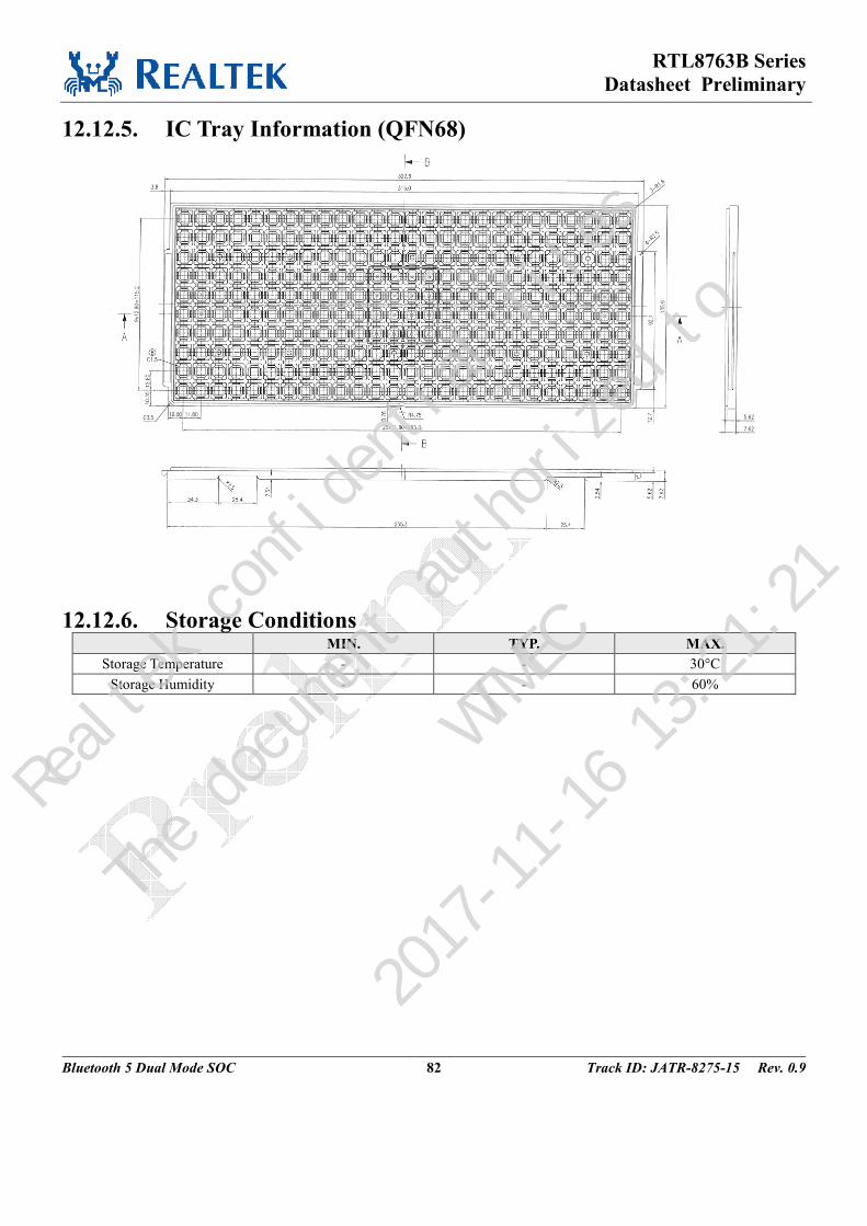
RTL8763B Series
Datasheet Preliminary
Bluetooth 5 Dual Mode SOC 82 Track ID: JATR-8275-15 Rev. 0.9
12.12.5. IC Tray Information (QFN68)
12.12.6. Storage Conditions MIN. TYP. MAX.
Storage Temperature - - 30°C
Storage Humidity - - 60%
Realtek confidential files
The document authorized to
WTMEC
2017-11-16 13:21:21
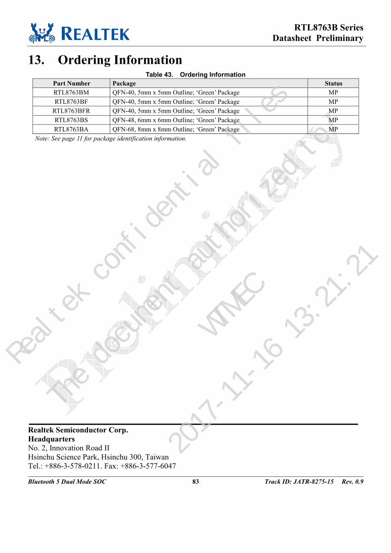
RTL8763B Series
Datasheet Preliminary
Bluetooth 5 Dual Mode SOC 83 Track ID: JATR-8275-15 Rev. 0.9
13. Ordering Information Table 43. Ordering Information
Part Number Package Status
RTL8763BM QFN-40, 5mm x 5mm Outline; ‘Green’ Package MP
RTL8763BF QFN-40, 5mm x 5mm Outline; ‘Green’ Package MP
RTL8763BFR QFN-40, 5mm x 5mm Outline; ‘Green’ Package MP
RTL8763BS QFN-48, 6mm x 6mm Outline; ‘Green’ Package MP
RTL8763BA QFN-68, 8mm x 8mm Outline; ‘Green’ Package MP
Note: See page 11 for package identification information.
Realtek Semiconductor Corp.
Headquarters
No. 2, Innovation Road II
Hsinchu Science Park, Hsinchu 300, Taiwan
Tel.: +886-3-578-0211. Fax: +886-3-577-6047
Realtek confidential files
The document authorized to
WTMEC
2017-11-16 13:21:21
RTL8763B Series
Datasheet Preliminary
Bluetooth 5 Dual Mode SOC 84 Track ID: JATR-8275-15 Rev. 0.9
www.realtek.com
Realtek confidential files
The document authorized to
WTMEC
2017-11-16 13:21:21