Embed Size (px)
Citation preview

RTE-V830-PCUser's Manual
Midas lab

RTE-V830-PC USER’ S MANUAL
1
REVISION HISTORY
Date of enforcement Revision Page Description
November 28, 1995 0.9 Preliminary issue
December 25, 1995 0.91 6, 7,...9, 10
Correction of error in which SW1 was written as SW2and vice versaCorrection of error related to descriptions about SW1(1-2 and 3-4) settings
February 5, 1996 0.92 14 Correction of errors in tables in Sections 6.1 and 6.2
November 23, 1996 1.01e 16
21
Correction of errors in tables in Sections 6.2(bit2-bit0 in port0 )Correction of errors in tables in Sections 7

RTE-V830-PC USER’ S MANUAL
2
CONTENTS
1. INTRODUCTION ...............................................................................................................4
1.1. NUMERIC NOTATION ..............................................................................................4
2. FEATURES AND FUNCTIONS..........................................................................................5
3. BOARD CONFIGURATION ...............................................................................................6
3.1. RESET SWITCH (SWRESET) ..................................................................................6
3.2. POWER SUPPLY CONNECTOR (JPOWER) ...........................................................6
3.3. SWITCH 1 (SW1)......................................................................................................6
3.4. SWITCH 2 (SW2)......................................................................................................7
3.5. LED...........................................................................................................................7
3.6. TEST PINS (TP)........................................................................................................7
3.7. SERIAL CONNECTOR (JSIO)...................................................................................8
3.8. CPU TEST PINS (J1) ................................................................................................8
3.9. CLOCK SOCKET (OSC1) .........................................................................................8
3.10. DRAM-SIMM SOCKETS ...........................................................................................9
3.11. ROM SOCKETS........................................................................................................9
4. INSTALLATION AND USE ..............................................................................................10
4.1. BOARD SETTING ...................................................................................................10
4.2. INSTALLATION ON THE ISA BUS..........................................................................11
4.3. STANDALONE USE OF THE BOARD ....................................................................12
5. HARDWARE REFERENCES ...........................................................................................13
5.1. MEMORY MAP .......................................................................................................13
5.2. I/O MAP ..................................................................................................................14
6. SYSTEM-I/O....................................................................................................................15
6.1. UART/TIMER (SCC2691)........................................................................................15
6.2. PIO (µPD71055)......................................................................................................15
6.3. OTHER PORTS ......................................................................................................19
7. JEXT BUS SPECIFICATION ...........................................................................................21
8. OTHER CPU RESOURCES.............................................................................................23
8.1. RESET-...................................................................................................................23
8.2. NMI- ........................................................................................................................23
9. MULTI MONITOR............................................................................................................24
9.1. MONITOR WORK RAM ..........................................................................................24
9.2. INTERRUPTS .........................................................................................................24
RTE-V830-PC USER’ S MANUAL
3
9.3. _INIT_SP SETTING ................................................................................................24
9.4. REMOTE CONNECTION ........................................................................................24
10. RTE COMMANDS ...........................................................................................................25
10.1. HELP (?) .................................................................................................................25
10.2. INIT .........................................................................................................................25
10.3. VER ........................................................................................................................25
10.4. INB, INH, AND INW ................................................................................................25
10.5. OUTB, OUTH, AND OUTW.....................................................................................26
10.6. DCTR COMMAND...................................................................................................26
10.7. ITCR COMMAND ....................................................................................................26
10.8. PLLCR COMMAND.................................................................................................26
10.9. CMCR COMMAND..................................................................................................26
11. APPENDIX DRAM TIMING............................................................................................27
11.1. DRAM INTERFACE OVERVIEW ............................................................................27
11.2. SIGNAL DESCRIPTIONS........................................................................................27
11.3. 32-BIT BUS MODE (SINGLE READ, NORMAL)......................................................28
11.4. 32-BIT BUS MODE (SINGLE READ, HIT) ...............................................................29
11.5. 32-BIT BUS MODE (SINGLE READ, NOHIT)..........................................................30
11.6. 32-BIT BUS MODE (SINGLE WRITE, NORMAL)....................................................31
11.7. 32-BIT BUS MODE (SINGLE WRITE, HIT) .............................................................32
11.8. 32-BIT BUS MODE (SINGLE WRITE, NOHIT)........................................................33
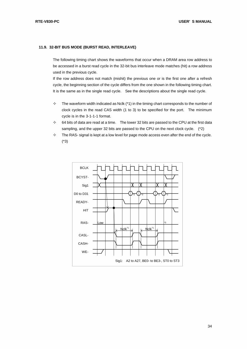
11.9. 32-BIT BUS MODE (BURST READ, INTERLEAVE)................................................34
11.10. 32-BIT BUS MODE (BURST WRITE, INTERLEAVE) ............................................35
11.11. 32-BIT BUS MODE (BURST READ, NONINTERLEAVE) ......................................36
11.12. 32-BIT BUS MODE (BURST WRITE, NONINTERLEAVE) ....................................37
11.13. 16-BIT BUS MODE (SINGLE READ).....................................................................38
11.14. 16-BIT BUS MODE (SINGLE WRITE)...................................................................40
11.15. 16-BIT BUS MODE (BURST READ, INTERLEAVE)..............................................41
11.16. 16-BIT BUS MODE (BURST WRITE, INTERLEAVE) ............................................42
11.17. 16-BIT BUS MODE (BURST READ, NONINTERLEAVE) ......................................43
11.18. 16-BIT BUS MODE (BURST WRITE, NONINTERLEAVE) ....................................44

RTE-V830-PC USER’ S MANUAL
4
1. INTRODUCTION
This manual describes the RTE-V830-PC, which is an evaluation board for the V830, NEC's
CPU. With the RTE-V830-PC, it is possible to develop and debug programs, and evaluate the
CPU performance, using the GreenHills Multi debugger. Communication with this debugger is
carried out using the IBM-PC/AT ISA bus or RS-232C serial interface. It is also possible to
expand memory and I/O units using local bus connectors provided on the evaluation board.
1.1. NUMERIC NOTATION
This manual represents numbers according to the notation described in the following table.
Hexadecimal and binary numbers are hyphenated at every four digits, if they are difficult to read
because of many digits being in each number.
Number Notation rule Example
Decimalnumber
Only numerals are indicated. "10" represents number 10 in decimal.
Hexa-decimalnumber
A number is suffixed with letter H. "10H" represents number 16 in decimal.
Binarynumber
A number is suffixed with letter B. "10B" represents number 2 in decimal.
Number Notation Rules

RTE-V830-PC USER’ S MANUAL
5
2. FEATURES AND FUNCTIONS
The overview of each function block of the RTE-V830-PC is shown below.
V830
ISA Bus
Local Bus
ISA BUS I/F
JEXTCONNECTOR
ORD-RAM S-RAM ROM
TIMER/SIOInternalControl
OR
RS-232CCONNECTOR
OR
PIO
USERHW
RTE-V830-PC Block Diagram
Features
• ROM: 256 Kbytes (64K x 16-bit EPROM x 2)
• SRAM: 512 Kbytes (64K x 16-bit SRAM x 4)
• DRAM: 8, 16, or 32 Mbytes (standard of 8 Mbytes) installed in two 72-pin SIMM sockets
• RS-232C port (9-pin D-SUB connector)
• Communication function supported using the ISA bus of a PC/AT or compatible
• Local bus connector for user-installed expansion equipment
• Processor pin connector enabling measurement of all CPU signals
• External reset switch provided on the rear panel
• Connection pins for ROM in-circuit debugger

RTE-V830-PC USER’ S MANUAL
6
3. BOARD CONFIGURATION
The physical layout of the major components on the RTE-V830-PC board is shown below. This
chapter explains each component.
RTE-V830-PC Board Top View
3.1. RESET SWITCH (SWRESET)
SWRESET is a reset switch. Pressing this switch causes the CPU to be reset.
3.2. POWER SUPPLY CONNECTOR (JPOWER)
When this board is to be used as a standalone, that is, without being inserted in an ISA bus slot,
the board should be supplied with power from an external power supply by connecting it to the
JPOWER connector.
The external power should be one rated as listed below.
Voltage: 5 V
Current: Maximum of 2 A (excluding the current supplied to the JEXT
connector)
Mating connector: Type A (5.5 mm in diameter)
Polarity:
GND
GND
+5V
+5V
[Caution] When attaching an external power supply to the board, be careful about its
connector polarity. When inserting the board into the ISA bus slot, do not attach the JPOWER
connector to an external power supply.
3.3. SWITCH 1 (SW1)
SW1 is a switch for general-purpose input ports. When SW1 is in the OFF position, it
represents 1. When it is in the ON position, it represents 0. See Section 6.2 for details.
SW2SCC/TIMER
SW RESET
JPOWERJEXT
JSIO
PLD
PIO
SW1
PLD
PLD
PLD
PLD
ROM(D16-31)
ROM(D0-15)
RAMRAM
V830
J1(1-36)
J1(37-72)
J1(73-108)
J1(109-144)
TP
OSC11pin
SIM-72pin X 2
POWERCS0CS1CS2CS3
TOVER

RTE-V830-PC USER’ S MANUAL
7
3.4. SWITCH 2 (SW2)
SW2 is a switch for selecting the I/O address of the ISA bus. Switch contacts 1 to 8
corresponds to ISA addresses A4 to A11, respectively (A12 to A15 are fixed at 0). This means
that the I/O address that can be selected ranges between 000xH and 0FFxH. When a switch
contact is open, it corresponds to 1. When it is closed, it corresponds to 0.
SW2 contact 1 2 3 4 5 6 7 8
ISA address A4 A5 A6 A7 A8 A9 A10 A11
SW2-to-ISA Address Correspondence
3.5. LED
The LEDs are used to indicate statuses, as listed below.
LED Description
POWER Lights when power is supplied to the RTE-V830-PC board.
CS0 Lights when the CS0 pin of the CPU is active (low).
CS1 Lights when the CS1 pin of the CPU is active (low).
CS2 Lights when the CS2 pin of the CPU is active (low).
CS3 Lights when the CS3 pin of the CPU is active (low).
TOVER Lights when a time-out occurs.
LED Indication
3.6. TEST PINS (TP)
Test pins are used to connect a ROM in-circuit debugger. They accept control signals from
the ROM in-circuit debugger. The following table lists the signal name and function related to
each test pin.
Signal Input/output
Function
RESET- Input When a low level is supplied to this test pin, the CPU is reset. Areset request signal from the ROM in-circuit debugger isconnected to the test pin. The test pin is pulled up with 1kΩ.
NMI- Input When a low level is supplied to this test pin, an NMI signal is givento the CPU. This signal can be masked by software. An NMIrequest (break request) signal from the ROM in-circuit debugger isconnected to the test pin. The test pin is pulled up with 1kΩ.
GND – – – This test pin is at a ground level. The ground level of the ROMin-circuit debugger is connected to the test pin.
Test Pin Functions

RTE-V830-PC USER’ S MANUAL
8
3.7. SERIAL CONNECTOR (JSIO)
JSIO is a connector for the RS-232C interface controlled by the serial controller (SCC2691). It
is a 9-pin D-SUB connector (D-SUB9) generally used with the PC/AT. All signals at this
connector are at RS-232C level. Its pin arrangement and signal assignment are shown and
listed below.
For connection signals connected to the host computer, the table gives the wirings for both the
D-SUB9 pins and D-SUB25 pins on the host side. (These are general cross-cable wirings.)
1
9876
5432
JSIO Pin Arrangement
Pin Signal name Input/output
Connector pin number onthe host side
D-SUB9 D-SUB25
1 NC2 RxD(RD) Input 3 23 TxD(SD) Output 2 34 DTR(DR) Output 1, 6 6, 85 GND 5 76 DSR(ER) Input 4 207 RTS(RS) Output 8 58 CTS(CS) Input 7 49 NC
JSIO Connector Signals
3.8. CPU TEST PINS (J1)
The CPU test pins are connected to the corresponding CPU pins. The test pin numbers
correspond to the CPU pin numbers on a one-to-one basis. The test pins can be used to
handle CPU signals for test purposes.
3.9. CLOCK SOCKET (OSC1)
The OSC1 socket is connected to an oscillator used to supply clock pulses to the CPU. The
V830 uses a PLL for system clock generation. The SW1-7 setting specifies the frequency of
the oscillator connected to the OSC1 socket. The frequency must be half or one-third the
internal clock frequency.
The oscillator connected to the OSC1 socket must be of an 8-pin DIP type (half type).
[Caution] When you have to cut an oscillator or crystal pin for convenience, be careful not to
cut it too short, or otherwise the frame (housing) of the oscillator or crystal may touch a tine in
the socket, resulting in a short-circuit occurring.

RTE-V830-PC USER’ S MANUAL
9
3.10. DRAM-SIMM SOCKETS
The RTE-V830-PC has DRAM-SIMM sockets used to install two 4 Mbytes (standard) of SIMMs.
Each socket can hold a 72-pin 4-, 8-, or 16-Mbyte SIMM (known as a module for DOS/V
machines), so it is easy to expand the capacity of DRAM. Select SIMM chips that meet the
access timing requirements listed in a table elsewhere. The selected SIMM chips must be of
the same model. The capacity of installed SIMMs can be detected using a PIO port. (See
Section 6.2.)
3.11. ROM SOCKETS
The RTE-V830-PC has ROM sockets to hold 40-pin ROM chips to provide standard 128 Kbytes
(64K x 16 bits). When the ROM chips used here are to be replaced, the access time should be
150 ns or less.
RTE-V830-PC USER’ S MANUAL
10
4. INSTALLATION AND USE
The RTE-V830-PC board is designed to be installed in the ISA bus slot of a PC/AT or compatible
(hereafter called the PC). However, it can also be used as a standalone, if it is powered from
an external power supply. When the board is used for testing purposes or with the Multi
debugger, communication software called RTE for Windows must be installed in the PC. Refer
to the RTE for Windows Installation Manual for installation and test methods.
4.1. BOARD SETTING
The RTE-V830-PC board has DIP switches. The DIP switches can be used to set up the
evaluation board. The switch layout is shown below.
Switches on the RTE-V830-PC Board
SW2 is a switch for selecting the I/O address of the ISA bus. Switch contacts 1 to 8 correspond
to ISA addresses A4 to A11, respectively (A12 to A15 are fixed at 0). This means that the I/O
address that can be selected ranges between 000xH and 0FFxH. When a switch contact is
open, it corresponds to 1. When it is closed, it corresponds to 0. Generally, SW2 is set to any
value between 20xH and 3FxH.
SW2contact
1 2 3 4 5 6 7 8
Address A4 A5 A6 A7 A8 A9 A10 A11 I/O address
ON/OFF
0 0 0 0 01
0 0 020xH(factory-set)
SW2-to-ISA I/O Address Correspondence
SW1 is a switch for general-purpose input ports. For the Multi monitor in the factory-installed
ROM, SW1 is used to set the RS-232C baud rate and profiler timer period.
SW1contact
1 2 Baud rate
Setting ONOFFONOFF
ONONOFFOFF
Not used38400 baud19200 baud 9600 baud (factory-set)
Baud Rate Setting
SW2SCC/TIMER
SWRESET
JPOWERJEXT
JSIO
PLD
PIO
SW1
PLD
PLD
PLD
PLD
ROM(D16-31)
ROM(D0-15)
RAMRAM
V830
J1(1-36)
J1(37-72)
J1(73-108)
J1(109-144)
TP
OSC11pin
SIM-72pin X 2
POWERCS0CS1CS2CS3
TOVER

RTE-V830-PC USER’ S MANUAL
11
SW1contact
3 4 Profiler period
Setting ONOFFONOFF
ONONOFFOFF
Timer is not used.200 Hz 5 ms100 Hz 10 ms60 Hz 16.67 ms (factory-set)
Profiler Period Setting
Contacts 5 and 6 of SW1 are not used for the Multi monitor (they are fixed at OFF).
SW1contact
7 CMODE (V830 pin)
Setting ONOFF
Triple modeDouble mode
CMODE Setting
SW1contact
8 SIZE16 (V830 pin)
Setting ONOFF
32-bit mode16-bit mode
SIZE16 Setting
4.2. INSTALLATION ON THE ISA BUS
When the RTE-V830-PC is installed in the ISA bus slot of the PC, power (+5V) is supplied from
the ISA bus to the board. In addition, the ISA bus can be used for communication with the
debugger, so programs are down-loaded at high speed.
The RTE-V830-PC can be installed in the ISA bus slot according to the following procedure.
Set the I/O address of the PC using a DIP switch on the board. Be careful not to specify
the same I/O address as used for any other I/O unit. See Section 4.1 for switch setting.
Turn off the power to the PC, open its housing, and confirm the ISA bus slot to be used. If
the slot is equipped with a rear panel, remove the rear panel.
Insert the board into the ISA bus slot. Make sure that the board does not touch any
adjacent board. Fasten the rear panel of the board to the housing of the PC with screws.
Turn on the power to the PC, and check that the POWER-LED on the board lights. If the
LED does not light, turn off the PC power immediately, and check the connection. If
the system does not start normally (for example, if an error occurs during installation of a
device driver), it is likely that the set I/O address is the same as one already in use.
Reconfirm the I/O address of the board by referring to the applicable manual of the PC or
the board.
When the system turns out to be normal, turn off the PC power again, and put back its
housing.

RTE-V830-PC USER’ S MANUAL
12
4.3. STANDALONE USE OF THE BOARD
When the RTE-V830-PC is used as a standalone rather than being installed in the PC, it
requires an external power supply. In addition, communication with the debugger is supported
only by the RS-232C interface. This configuration is useful when the host debugger used with
the board is not one in the PC/AT or compatible as well as when the board is used for hardware
confirmation and expansion.
The RTE-V830-PC can be used as a standalone according to the following procedure.
Get an RS-232C cable for connection with the host and an external power supply (+5 V, 1
A) on hand. Especially for the power supply, watch for its voltage and connector polarity.
In addition, attach spacers to the four corners of the board, so it will not pose any problem
wherever it is installed. See Sections 3.7 and 3.2 for RS-232C cable connection and the
power supply connector, respectively.
Set the RS-232C baud rate using a DIP switch on the board. See Section 4.1 for switch
setting.
Connect the board to the host via an RS-232C cable. Also connect an external power
supply to the JPOWER connector, then check that the POWER-LED on the board lights.
If the LED does not light, turn off the power immediately, and check the connection.

RTE-V830-PC USER’ S MANUAL
13
5. HARDWARE REFERENCES
This chapter describes the hardware of the RTE-V830-PC.
5.1. MEMORY MAP
The memory assignment of the board is shown below.
0000-0000
4FFF-FFFF
8000-0000
4000-0000
7E00-0000
0000-0FFF
CS0 space
6000-0000
6010-0000
6020-0000
600F-FFFF
601F-FFFF
60FF-FFFF
80FF-FFFF
C000-0000BFFF-FFFF
61FF-FFFF6200-0000
6FFF-FFFF
XE80-0000XE7F-FFFF
XE00-0000
XEFF-FFFFXF00-0000
XFFB-FFFFXFFC-0000FE00-1000
XFFF-FFFFFFFF-FFFF
Image of XE7F-0000 to XE00-0000
Image ofXFFC-0000 toXFFF-FFFF
Accessinhibited
CS1 space
CS2 space
CS3 space (*1)
DRAM
Reserved
SRAM
EXT-BUS
SYSTEM-I/O
ROM
0000-1000
0FFF-FFFF
2FFF-FFFF
2000-0000
3000-0000
Built-in data RAM
3FFF-FFFF
CS1 space
CS2 space
CS3 space
7000-0000
7DFF-FFFF
5FFF-FFFF
5000-0000
6000-0000
6FFF-FFFF
7FFF-FFFF
Accessinhibited
Accessinhibited
Accessinhibited
FDFF-FFFFFE00-0000FE00-0FFF
CS0 space
Built-in instructionRAM
Cacheablearea
Cacheablearea
Un-cacheablearea
Cacheablearea
6100-0000
Accessinhibited
ReservedX000-0000
XFFF-FFFF
X000-0000
X1FF-FFFFX200-0000
XFFF-FFFFImage of X000-0000 to X1FF-FFFF
*1 Access to the CS3 space at 3000-0000 to 3FFF-FFF isinhibited.
Memory Map
DRAM spaces (0000-0000H to 01FF-FFFFH and 4000-0000H to 41FF-FFFFH)
These are spaces in 72-pin SIMM chips mounted on the RTE-V830-PC board. Two 4-Mbyte
SIMM chips are used in a standard configuration. They can be replaced with 8- or 16-Mbyte
SIMM chips for memory expansion. It is possible to specify RAS, CAS, and precharge
widths. (See Section 6.2.)
Reserved and access-inhibited spaces
Do not attempt to access these spaces.

RTE-V830-PC USER’ S MANUAL
14
EXT-BUS space (6010-0000H to 601F-FFFFH)
This space is used for a hardware expansion board connected to the JEXT connector on the
RTE-V830-PC. See Chapter 7 for details of the EXT-BUS.
SYSTEM-I/O space (6100-0000H to 61FF-FFFFH)
This space is assigned to I/O devices for controlling each function on the board. It acts as
memory-mapped I/O units. See Chapter 6 for details..
SRAM space (FE00-0000H to FE07-FFFFH and 7E00-0000H to 7E07-FFFFH)
This space is provided in SRAM on the board. Its capacity is 512 Kbytes. SRAM can be
accessed with no wait state. Wait states can be specified for read and write cycles
separately. (See Section 6.2.)
ROM space (FFFC-0000H to FFFF-FFFFH and 7FFC-0000H to 7FFF-FFFFH)
This space is provided in ROM on the board. Its storage capacity is 256 Kbytes. Ten wait
states are inserted in a ROM access cycle during ready signal control. If the external bus
clock frequency is 50 MHz, the access time of the ROM must be 150 ns or less.
The standard ROM chip that is factory-set contains the Multi monitor.
5.2. I/O MAP
The I/O space in the V830-CPU is not used by the RTE-V830-PC. The I/O registers used for
control purposes are allocated in the memory-mapped SYSTEM-I/O space.

RTE-V830-PC USER’ S MANUAL
15
6. SYSTEM-I/O
SYSTEM-I/O is an I/O device mapped in a memory space. The I/O devices include the
UART/TIMER, PIO, and ISA bus interface. (No description about the ISA bus interface is
included.)
6.1. UART/TIMER (SCC2691)
The SCC2691 UART receiver/transmitter LSI chip produced by PHILIPS Signetics is used as the
UART/TIMER. Because the SCC2691 has a 3-character buffer in the receiver section, it is
possible to minimize chances of an overrun error occurring during reception. Moreover, a
3.6864 MHz oscillator is connected across the X1 and X2 pins. It, in conjunction with a 16-bit
counter in the SCC2691, enables measurement of about 271 ns to 17.8 ms.
Each register in the SCC2691 is assigned as listed below. Refer to the applicable SCC2691
manual for the function of each register.
Address Read access Write access
6100-0400h MR1, MR2 MR1, MR2
6100-0404h SR CSR
6100-0408h Reserved CR
6100-040Ch RHR THR
6100-0410h Reserved ACR
6100-0414h ISR IMR
6100-0418h CTU CTUR
6100-041Ch (CTL) CTLR
SCC2691 Register Mapping
The general-purpose output pin (MPO) and input pin (MPI) are used as RTS (RS) and CTS (CS),
respectively. DTR (DR) and DSR (ER) are controlled by the PIO. See Section 6.2 for details.
The SCC2691 is reset at a system reset (see Section 8.1).
6.2. PIO (µPD71055)
The µPD71055 produced by NEC is installed as a PIO. The µPD71055 is compatible with the
i8255 produced by Intel. It has three parallel ports. These ports are used for various types of
control. Each register of the PIO is assigned as listed below.
Address Read access Write access
6100-0800h PORT0 PORT0
6100-0804h PORT1 PORT1
6100-0808h PORT2 PORT2
6100-080Ch --------- COMMAND REG
PIO Register Mapping
The PIO ports are reset at a system reset. When reset, all these ports are set as input, so the
signal state of bits used for output is set to a high level, using a pull-up resistor. The following
table lists the way each port is used.

RTE-V830-PC USER’ S MANUAL
16
Bit7 Bit6 Bit5 Bit4 Bit3 Bit2 Bit1 Bit0
PORT0 SRAMRDWIDE1
SRAMRDWIDE0
SRAMWRWIDE1
SRAMWRWIDE0
INTERLEAVE Reserved field 1
Output
PORT1 PCWIDE1 PCWIDE0 RDCASWIDE1
RDCASWIDE0
WRCASWIDE0
MINRASWIDE[2..0]
Output
PORT2 PD[2..1] TOVERF- DSR- DTR- NMIMASK TOVERCLR- Reservedfield 1
Input Output
PIO Bit Assignment
The following paragraphs detail each port bit.
Port 0: Internal control port (output).....61000800h
P07 P06 P05 P04 P03 P02 P01 P00
SRAMRDWIDE1
SRAMRDWIDE0
SRAMWRWIDE1
SRAMWRWIDE0
INTERLEAVE Reserved
Reserved field 1: All the three bits in this field are reserved for the system. Once they are
initialized to 1, do not change them.
INTERLEAVE: This bit specifies whether to use the noninterleave emulation mode.
When the bit is 1, the DRAM is put in the normal mode. When it is 0,
the DRAM is put in the noninterleave emulation mode.
SRAMWRWIDE1..0: These bits specify the number of wait states to be inserted in an SRAM
write cycle.
SRAMWRWIDE1 SRAMWRWIDE0 Function
0 0 No wait state is inserted in an SRAM write cycle.
0 1 One wait state is inserted in an SRAM write cycle.
1 0 Two wait states are inserted in an SRAM write cycle.
1 1 Three wait states are inserted in an SRAM write cycle.
SRAMRDWIDE1..0: These bits specify the number of wait states to be inserted in an SRAM
read cycle.
SRAMRDWIDE1 SRAMRDWIDE0 Function
0 0 No wait state is inserted in an SRAM read cycle.
0 1 One wait state is inserted in an SRAM read cycle.
1 0 Two wait states are inserted in an SRAM read cycle.
1 1 Three wait states are inserted in an SRAM read cycle.

RTE-V830-PC USER’ S MANUAL
17
Port 1: DRAM access condition setting output port (input).....61000804h
P17 P16 P15 P14 P13 P12 P11 P10
PRCWIDE1
PRCWIDE0
RDCASWIDE1
RDCASWIDE0
WRCASWIDE0
MINRASWIDE2
MINRASWIDE1
MINRASWIDE0
MINRASWIDE2..0: These bits specify the minimum RAS width for DRAM operations.
RASWIDE2
RASWIDE1
RASWIDE0
Function
0 0 0 This bit combination shall not be specified.
0 0 1 This bit combination shall not be specified.
0 1 0 The minimum RAS width is specified to be two CPU busclock cycles.
0 1 1 The minimum RAS width is specified to be three CPU busclock cycles.
1 0 0 The minimum RAS width is specified to be four CPU busclock cycles.
1 0 1 This bit combination shall not be specified.
1 1 0 This bit combination shall not be specified.
1 1 1 This bit combination shall not be specified.
WRCASWIDE0: This bit specifies the CAS width for DRAM write operations.
WRCASWIDE0 Function
0 The CAS width for a write operation is specified to be one CPU bus clockcycle.
1 The CAS width for a write operation is specified to be two CPU bus clockcycles.
RDCASWIDE1..0: These bits specify the CAS width for DRAM read operations.
RDCASWIDE1 RDCASWIDE0 Function
0 0 This bit combination shall not be specified.
0 1 The CAS width for a read operation is specified to be oneCPU bus clock cycle.
1 0 The CAS width for a read operation is specified to be twoCPU bus clock cycles.
1 1 The CAS width for a read operation is specified to be threeCPU bus clock cycles.
RTE-V830-PC USER’ S MANUAL
18
PRCWIDE1..0: These bits specify the precharge width for DRAM operations.
PRCWIDE1 PRCWIDE0 Function
0 0 This bit combination shall not be specified.
0 1 The precharge width is specified to be one CPU bus clockcycle.
1 0 The precharge width is specified to be two CPU bus clockcycles.
1 1 The precharge width is specified to be three CPU bus clockcycles.
Port 2: Internal control port (output).....61000808h
P23 P22 P21 P20
DTR- NMIMASK TOVERFCLR- Reservedfield 1
Reserved field 1: The bit in this field is reserved for the system. Once the bit is initialized to 1,
do not change it.
TOVERCLR-: This is a control bit used to clear TOVERF- in bit 5 of port 2. It should be
initialized to 1 and usually kept to be 1. When TOVERF- is to be cleared,
the bit should be rest to 0, then set back to 1.
NMIMASK: This bit is used to mask an NMI signal input to the CPU. When the bit is 1,
the NMI signal is masked at a gate. The bit should be initialized to 1.
When an NMI becomes acceptable, the bit should be reset to 0. In the Multi
monitor, it is initialized to 1.
DTR-: This bit controls the DTR signal output from the JSIO connector. The
inverted state of this bit is converted to the RS-232C level and output to the
JSIO connector.
Port 2: Internal control port (input).....61000808h
P27 P26 P25 P24
PD2 PD1 TOVERF- DSR-
DSR-: This bit indicates the state of the DSR signal input from the JSIO connector. The
state of this bit represents the inverted state of the DSR signal at the JSIO
connector.
TOVERF-: This bit becomes 0, when 30 or more bus cycles occur to result in a time-out. The
flag is cleared (to 1), using bit 1 (TOVERCLR-) of port 2.
PD[2..1]: PD[2..1] of a DRAM (72-pin SIMM) chip mounted on the board can be read-
accessed. The states of these bits indicate the size of the DRAM area. The
following table lists the relationships between PD[2..1] and the DRAM capacity.

RTE-V830-PC USER’ S MANUAL
19
PD[2] PD[1] DRAM capacity
0 0 4 Mbytes
0 1 Reserved
1 0 16 Mbytes
1 1 8 Mbytes
PD[2..1] and DRAM Capacity
Ports 0 to 2: Control ports.....6100080Ch
Ports 0, 1, and 2 belong to the µPD71055. These ports are initialized by writing to the indicated
location.
6.3. OTHER PORTS
Port 3: 7-segment LED display data output port (output).....61000C00h
P17 P16 P15 P14 P13 P12 P11 P10
DPseg Gseg Fseg Eseg Dseg Cseg Bseg Aseg
Port 4: DIP SW1 state read port (input).....61000C04h
P17 P16 P15 P14 P13 P12 P11 P10
SW1-8 SW1-7 SW1-6 SW1-5 SW1-4 SW1-3 SW1-2 SW1-1
SIZE16B CMODE no use no use TIM1 TIM0 BPS1 BPS0
SW1-[8..1]: The states of SW1 mounted on the board can be read-accessed. SW1-1
corresponds to contact 1 of SW1, and SW1-2 corresponds to contact 2 of SW1,
and so on. When a switch is ON, the corresponding bit is 0, and when it is OFF,
the corresponding bit is 1.
BPS1 BPS0 Baud rate
ON ON 9600 bps
ON OFF 19200 bps
OFF ON 38400 bps
OFF OFF don’ t use
A
B
C
D
E
F
G
DP

RTE-V830-PC USER’ S MANUAL
20
TIM1 TIM0 Timer rate
ON ON No timer is used.
ON OFF 200 Hz ( 5 ms)
OFF ON 100 Hz (10 ms)
OFF OFF 60 Hz (16.67 ms)
CMODE: The multiplication factor for the internal clock frequency (triple for ON and double
for OFF)
SIZE16B: Bus size setting (32 bits for ON and 16 bits for OFF)

RTE-V830-PC USER’ S MANUAL
21
7. JEXT BUS SPECIFICATION
The JEXT is a connector which is used to expand memory and I/O units. The local bus on this
board is connected to the JEXT connector.
The following tables list the pin arrangement of the JEXT connector and the functions of each
signal. The timing relationships between the signals are also shown below.
Number Signal name Number Signal name Number Signal name Number Signal name
1 +5V 2 +5V 31 GND 32 GND
3 D0 4 D1 33 A8 34 A9
5 D2 6 D3 35 A10 36 A11
7 D4 8 D5 37 A12 38 A13
9 D6 10 D7 39 A14 40 A15
11 GND 12 GND 41 +5V 42 +5V
13 D8 14 D9 43 A16 44 A17
15 D10 16 D11 45 A18 46 A19
17 D12 18 D13 47 BHE- 48 GND
19 D14 20 D15 49 GND 50 RD-
21 +5V 22 +5V 51 WR- 52 RESET-
23 A0 24 A1 53 GND 54 GND
25 A2 26 A3 55 READY 56 INT-
27 A4 28 A5 57 GND 58 GND
29 A6 30 A7 59 CPUCLK 60 GND
JEXT Connector Pin Arrangement
Signalname
Input/output
Function
A[0..19] Output Address bus signal, which is originally the CPU address signalreceived at a buffer.
BHE- Output Byte high enable signal, which is originally the CPU UBE- signalreceived at a buffer.
D[0..15] Input/output
Data bus signal, which is originally the CPU data bus signal receivedat a buffer.It is pulled up with a 10 kΩ resistor on the board.
RD- Output Read cycle timing signal, which becomes active only when the JEXTspace is accessed.
WR- Output Write cycle timing signal, which becomes active only when the JEXTspace is accessed.
READY Input Signal indicating the end of a cycle. It is valid only for the JEXTspace.To have the CPU recognize READY securely, it is necessary to keepREADY active until RD- or WR- becomes inactive. It is pulled upwith a 10 kΩ resistor on the board.
INT- Input Active-low interrupt request signal, which is connected to the INT pinof the CPU via a interrupt controller(vector 11 is occurred). It ispulled up with a 10 kΩ resistor on the board.
RESET- Output Active-low system reset signalCLK Output Clock signal, which is connected to the CLKOUT pin of the V830 via
a buffer.
JEXT Connector Signals

RTE-V830-PC USER’ S MANUAL
22
RD-
A[0..19]BHE-
T1 T2
Write cycleRead cycle
READY
D[0..15]
WR-
T9T8
Dout
High
T7
Din
RD-
A[0..19]BHE-
T10
T12
T15
READY
D[0..15]
WR-
T17T16 T18
T6
High
T14
T3
T4
T11
T13
T5
JEXT Bus Cycle
Symbol Description Min. (ns) Max. (ns)
T1 RD address setup time 0
T2 RD address hold-up time 0
T3 RD cycle time 50
T4 RD cycle interval 20
T5 RD data setup time 15
T6 RD data hold time 0
T7 RD READY WAIT setup time 0
T8 RD READY setup time 0
T9 RD READY hold time 0
T10 WR address setup time 0
T11 WR address hold time 20
T12 WR cycle time 50
T13 WR cycle interval 20
T14 WR data delay time 20
T15 WR data hold time 20
T16 WR READY WAIT setup time 0
T17 WR READY setup time 0
T18 WR READY hold time 0
JEXT Bus AC Specifications
2
13
4
5
6
7
820
19
18
17
16
15
14
13
12
11
10
9
22
2123
24
25
26
27
2840
39
38
37
36
35
34
33
32
31
30
294143
44
45
46
47
4860
59
58
57
56
55
54
53
52
51
50
49
41
JEXT Pin Arrangement

RTE-V830-PC USER’ S MANUAL
23
8. OTHER CPU RESOURCES
8.1. RESET-
The factors listed below trigger a CPU reset. These factors reset the CPU. They also
system-reset the board control circuit.
• Power-on reset: Occurs when the power to the board is switched on.
• Reset request from the TP: Input at the RESET- pin of TP. See Section 3.6 for details.
• Reset by the SWRESET: Generated by the reset switch (SWRESET) on the rear panel of
the board.
• Reset request from the host: Sent via the ISA bus.
8.2. NMI-
An NMI to the CPU occurs as follows:
• SCC2691 interrupt: When the interrupt request output (INTR-) of the SCC2691 becomes
active, an NMI occurs (see Section 6.1).
• NMI request from a TP: A reset occurs when the NMI test pin receives an input. See
Section 3.6 for details.
• Request from the ISA bus: An NMI is used for communication control via the ISA bus.
An NMI signal can be masked hardwarewise. See descriptions about NMIMASK in Section 6.2
for how to mask an NMI signal. NMI masking based on NMIMASK is valid for all of the above
NMI requests.
The following procedure applies when an NMI occurs.
Set the NMIMASK of the PIO to 1 to mask the NMI hardwarewise.
Check the source of the NMI (ISR of the SCC2691 or TOVERF of the PIO).
Perform NMI processing for the interrupt source, and clear the request.
Reset the NMIMASK of the PIO to 0 to reset the mask.
Return from NMI processing.
RTE-V830-PC USER’ S MANUAL
24
9. Multi MONITOR
The ROM chip on the board is incorporated with the Multi monitor. The following cautions
should be observed when the board is connected to the Multi server as the host.
9.1. MONITOR WORK RAM
The monitor uses the first 64-KB area in the SRAM as work RAM. In other words, user
programs are not allowed to use logical addresses FE07-0000H to FE07-FFFFH.
9.2. INTERRUPTS
When running on the Multi monitor, user programs cannot use interrupts at present.
9.3. _INIT_SP SETTING
_INIT_SP (stack pointer initial value) is set to FE06-FFFCH (highest SRAM address) by the
monitor. (_INIT_SP can be changed in the Multi environment.)
9.4. REMOTE CONNECTION
Either serial or ISA bus connection can be selected for operation with the Multi server. To
switch from serial connection to ISA bus connection or vice versa, it is necessary to reset the
monitor (by pressing the reset switch on the rear panel) and run the Check RTE utility of RTE for
Windows.

RTE-V830-PC USER’ S MANUAL
25
10. RTE COMMANDS
When the monitor and server are connected, the TARGET window is opened. The RTE
commands can be issued in this window. The following table lists the RTE commands.
Command Description
HELP or ? Displays help messages.
INIT Initializes.
VER Displays the version number.
INB, INH, or INW I/O read
OUTB, OUTH, or
OUTW
I/O write
DCTR, INTR, PLLCR,
or CMCR
Changes or displays the internal
registers.
RTE Commands
Some commands require parameters. All numeric parameters such as addresses and data
are assumed to be hexadecimal numbers. The following numeric representations are invalid:
0x1234 1234H $1234
10.1. HELP (?)
<Format> HELP [command-name]
Displays a list of RTE commands and their formats. A question mark (?) can also be used in
place of the character string HELP. If no command name is specified in the parameter part, the
HELP command lists all usable commands.
<Example> HELP SFR
Displays help messages for the SFR command.
10.2. INIT
<Format> INIT
Initializes the RTE environment. Usually, this command should not be used.
10.3. VER
<Format> VER
Displays the version number of the current RTE environment.
10.4. INB, INH, AND INW
<Format> INB [address]
INH [address]
INW [address]
Read an I/O register. The INB, INH, and INW commands access in byte, halfword, and word
units, respectively. If an address is omitted, the previous address is assumed.
<Example> INB 1000
Reads a byte from an I/O register at 1000H.

RTE-V830-PC USER’ S MANUAL
26
10.5. OUTB, OUTH, AND OUTW
<Format> OUTB [[address] data]
OUTH [[address] data]
OUTW [[address] data]
Write to an I/O register. The OUTB, OUTH, and OUTW commands access in byte, halfword,
and word units, respectively. If an address or data is omitted, the previous address or data is
assumed.
<Example> OUTH 2000 55AA
Writes the halfword 55AAH to 2000H.
10.6. DCTR COMMAND
<Format> DCTR [ALL]
Displays the contents of DCTR registers. There are 256 DCTR registers. Among these 256
registers, the contents of the registers whose valid bit is on are displayed except when ALL is
specified. If ALL is specified, the contents of all DCTR registers are displayed. The DCTR
registers are mapped on the I/O space f2000000h-f2000fffh.
10.7. ITCR COMMAND
<Format> ITCR [ALL]
Displays the contents of ICTR registers. There are 128 ICTR registers. Among these 128
registers, the contents of the registers whose valid bit is on are displayed except when ALL is
specified. If ALL is specified, the contents of all ICTR registers are displayed. The ICTR
registers are mapped on the I/O space fa000000h-fa000fffh.
10.8. PLLCR COMMAND
<Format> PLLCR
Displays the value in the PLL control register.
10.9. CMCR COMMAND
<Format> CMCR[=]VALUE
Specifies a value in the cache memory control register (CMCR).

RTE-V830-PC USER’ S MANUAL
27
11. APPENDIX DRAM TIMING
11.1. DRAM INTERFACE OVERVIEW
The DRAM consists of two 32-bit banks. In the ordinary mode (interleave mode), the banks are
accessed alternately so that the access time during burst access can be reduced.
The DRAM is accessed in the page mode. The RAS signal for the DRAM is kept active as long
as the same row address is being accessed; access is controlled only by manipulating the CAS
signal. This method can reduce the access time if access continues with the same row
address.
11.2. SIGNAL DESCRIPTIONS
The signals used for waveforms described in this chapter are defined as follows:
BCLK: Bus clock pulse input to the CPU
BCYST-: Bus cycle start signal output from the CPU
READY-: Ready signal input to the CPU
HIT: Signal that indicates whether a row address is the same as one used in the previous
cycle, because the DRAM is used in the page mode. This signal is generated by the
DRAM control circuit.
RAS-: RAS signal input to the DRAM
CASL-: CAS signal input to the lower 32-bit bank of DRAM. One CASL- signal is provided
for each byte in the word (hence, CASL0 to CASL3-)
CASH-: CAS signal input to the upper 32-bit bank of DRAM. One CASH- signal is provided
for each byte in the word (hence, CASH0 to CASH3-)
WE-: WE signal input to the DRAM

RTE-V830-PC USER’ S MANUAL
28
11.3. 32-BIT BUS MODE (SINGLE READ, NORMAL)
The following timing chart shows the waveforms that occur when an area is accessed in a single
read cycle during the 32-bit bus mode for the first time after a reset or when the area is accessed
after the precharge time has elapsed since the end of a refresh cycle (normal).
² The waveform widths indicated as Mclk (*1) and Nclk (*2) in the timing chart correspond to
the number of clock cycles in the RAS width (2 to 4) and read CAS width (1 to 3) to be set
for the port, respectively. The minimum cycle is one wait state.
² The RAS- signal is kept at a low level for page mode access even after the end of the cycle.
(*3)
² The upper and lower 32-bit banks are read simultaneously. The CPU is supplied with
data from an appropriate bank according to the state of A2.
WE-
CASH-
CASL-
*3
Nclk*2
Mclk*1
HIT
RAS-
Sig1: A2 to A27, BE0- to BE3-, ST0 to ST3
Sig1
D0 to D31
READY-
BCYST-
BCLK

RTE-V830-PC USER’ S MANUAL
29
11.4. 32-BIT BUS MODE (SINGLE READ, HIT)
The following timing chart shows the waveforms that occur when a row address to be accessed
in a single read cycle during the 32-bit bus mode matches (hit) a row address used in the
previous cycle.
² The waveform width indicated as Nclk (*1) in the timing chart corresponds to the number of
clock cycles in the read CAS width (1 to 3) to be specified for the port. The minimum
cycle is one wait state.
² The RAS- signal is kept at a low level for page mode access even after the end of the cycle.
(*2)
² The upper and lower 32-bit banks are read simultaneously. The CPU is supplied with
data from an appropriate bank according to the state of A2.
WE-
CASH-
CASL-
*2Low
Nclk*1
HIT
RAS-
Sig1: A2 to A27, BE0- to BE3-, ST0 to ST3
Sig1
D0 to D31
READY-
BCYST-
BCLK

RTE-V830-PC USER’ S MANUAL
30
11.5. 32-BIT BUS MODE (SINGLE READ, NOHIT)
The following timing chart shows the waveforms that occur when a row address to be accessed
in a single read cycle during the 32-bit bus mode does not match (nohit) a row address used in
the previous cycle.
² The waveform widths indicated as Lclk (*1), Mclk (*2), and Nclk (*3) in the timing chart
correspond to the number of clock cycles in the precharge width (1 to 3), RAS width (2 to 4),
and read CAS width (1 to 3) to be specified for the port. The minimum cycle is three wait
states.
² The RAS- signal is kept at a low level for page mode access even after the end of the cycle.
(*4)
² The upper and lower 32-bit banks are read simultaneously. The CPU is supplied with
data from an appropriate bank according to the state of A2.
WE-
CASH-
CASL-
*4Low
Nclk*3
HIT
RAS-
Sig1: A2 to A27, BE0- to BE3-, ST0 to ST3
Sig1
D0 to D31
READY-
BCYST-
BCLK
Mclk*2Lclk*1

RTE-V830-PC USER’ S MANUAL
31
11.6. 32-BIT BUS MODE (SINGLE WRITE, NORMAL)
The following timing chart shows the waveforms that occur when an area is accessed in a single
write cycle during the 32-bit bus mode for the first time after a reset or when the area is
accessed after the precharge time has elapsed since the end of a refresh cycle (normal).
² The waveform widths indicated as Mclk (*1) and Nclk (*2) in the timing chart correspond to
the number of clock cycles in the RAS width (2 to 4) and write CAS width (1 or 2) to be set
for the port, respectively. The minimum cycle is one wait state.
² The RAS- signal is kept at a low level for page mode access even after the end of the cycle.
(*3)
² The CASL- or CASH- signal, whichever corresponds to the appropriate byte position in the
appropriate bank, becomes active according to the state of A2 and bus enable signals
BE0- to BE3-. (*4)
WE-
CASH-
CASL-
*4
*4
*3
Nclk*2
Mclk*1
HIT
RAS-
Sig1: A2 to A27, BE0- to BE3-, ST0 to ST3
Sig1
D0 to D31
READY-
BCYST-
BCLK

RTE-V830-PC USER’ S MANUAL
32
11.7. 32-BIT BUS MODE (SINGLE WRITE, HIT)
The following timing chart shows the waveforms that occur when a row address to be accessed
in a single write cycle during the 32-bit bus mode matches (hit) a row address used in the
previous cycle.
² The waveform width indicated as Nclk (*1) in the timing chart corresponds to the number of
clock cycles in the write CAS width (1 or 2) to be specified for the port. The minimum
cycle is one wait state.
² The RAS- signal is kept at a low level for page mode access even after the end of the cycle.
(*2)
² The CASL- or CASH- signal, whichever corresponds to the appropriate byte position in the
appropriate bank, becomes active according to the state of A2 and bus enable signals
BE0- to BE3-. (*3)
WE-
CASH-
CASL-
*3
*3
*2
Nclk*1
Low
HIT
RAS-
Sig1: A2 to A27, BE0- to BE3-, ST0 to ST3
Sig1
D0 to D31
READY-
BCYST-
BCLK

RTE-V830-PC USER’ S MANUAL
33
11.8. 32-BIT BUS MODE (SINGLE WRITE, NOHIT)
The following timing chart shows the waveforms that occur when a row address to be accessed
in a single write cycle during the 32-bit bus mode does not match (nohit) a row address used in
the previous cycle.
² The waveform widths indicated as Lclk (*1), Mclk (*2), and Nclk (*3) in the timing chart
correspond to the number of clock cycles in the precharge width (1 to 3), RAS width (2 to 4),
and write CAS width (1 or 2) to be specified for the port. The minimum cycle is three wait
states.
² The RAS- signal is kept at a low level for page mode access even after the end of the cycle.
(*4)
² The CASL- or CASH- signal, whichever corresponds to the appropriate byte position in the
appropriate bank, becomes active according to the state of A2 and bus enable signals
BE0- to BE3-. (*5)
WE-
CASH-
CASL-
*5
*5
*4
Nclk*3
HIT
RAS-
Sig1: A2 to A27, BE0- to BE3-, ST0 to ST3
Sig1
D0 to D31
READY-
BCYST-
BCLK
Mclk*2Lclk*1
RTE-V830-PC USER’ S MANUAL
34
11.9. 32-BIT BUS MODE (BURST READ, INTERLEAVE)
The following timing chart shows the waveforms that occur when a DRAM area row address to
be accessed in a burst read cycle in the 32-bit bus interleave mode matches (hit) a row address
used in the previous cycle.
If the row address does not match (mishit) the previous one or is the first one after a refresh
cycle, the beginning section of the cycle differs from the one shown in the following timing chart.
It is the same as in the single read cycle. See the descriptions about the single read cycle.
² The waveform width indicated as Nclk (*1) in the timing chart corresponds to the number of
clock cycles in the read CAS width (1 to 3) to be specified for the port. The minimum
cycle is in the 3-1-1-1 format.
² 64 bits of data are read at a time. The lower 32 bits are passed to the CPU at the first data
sampling, and the upper 32 bits are passed to the CPU on the next clock cycle. (*2)
² The RAS- signal is kept at a low level for page mode access even after the end of the cycle.
(*3)
WE-
CASH-
CASL-
*2 *2*2*2
*3Low
Nclk*1Nclk*1
HIT
RAS-
Sig1: A2 to A27, BE0- to BE3-, ST0 to ST3
Sig1
D0 to D31
READY-
BCYST-
BCLK

RTE-V830-PC USER’ S MANUAL
35
11.10. 32-BIT BUS MODE (BURST WRITE, INTERLEAVE)
The following timing chart shows the waveforms that occur when a DRAM area row address to
be accessed in a burst write cycle during the 32-bit bus interleave mode matches (hit) a row
address used in the previous cycle.
If the row address does not match (mishit) the previous one or is the first one after a refresh
cycle, the beginning of the cycle differs from the one shown in the following timing chart. It is
the same as in the single write cycle. See the descriptions about the single write cycle.
² The waveform width indicated as Nclk (*1) in the timing chart corresponds to the number of
clock cycles in the write CAS width (1 or 2) to be specified for the port. The minimum
cycle is in the 3-1-1-2 format.
² Write data is through-latched at the DRAM control circuit, then passed to the DRAM. So,
the setup and hold time for the falling edge of the CAS signal is guaranteed.
² The RAS- signal is kept at a low level for page mode access even after the end of the cycle.
(*3)
WE-
CASH-
CASL-
*2
*3
Nclk-1*1Nclk-1*1
Nclk*1
Low
HIT
RAS-
Sig1: A2 to A27, BE0- to BE3-, ST0 to ST3
Sig1
D0 to D31
READY-
BCYST-
BCLK
*2
Nclk-1*1
*2
Nclk*1
Nclk*1
Nclk*1
Nclk*1

RTE-V830-PC USER’ S MANUAL
36
11.11. 32-BIT BUS MODE (BURST READ, NONINTERLEAVE)
The following timing chart shows the waveforms that occur when a DRAM area row address to
be accessed in a burst read cycle during the 32-bit bus noninterleave mode matches (hit) a row
address used in the previous cycle.
This noninterleave mode is the one attained by simulation using the interleave circuit under
READY control. It may vary from the actual noninterleave cycle.
If the row address does not match (mishit) a row address used in the previous cycle or is the first
one after a refresh cycle, the beginning section of the cycle differs from the one shown in the
following timing chart. It is the same as in the single read cycle. See the descriptions about
the single read cycle.
² The waveform width indicated as Nclk (*1) in the timing chart corresponds to the number of
clock cycles in the read CAS width (1 to 3) to be specified for the port. The minimum
cycle is in the 3-2-2-2 format.
² 64 bits of data are read at a time. The lower 32 bits are passed to the CPU at the first data
sampling, and the upper 32 bits are passed to the CPU on the next clock cycle. (*2)
² The RAS- signal is kept at a low level for page mode access even after the end of the cycle.
(*3)
WE-
CASH-
CASL-
*2 *2*2*2
*3Low
Nclk*1Nclk*1
Sig1: A2 to A27, BE0- to BE3-, ST0 to ST3
HIT
RAS-
Sig1
D0 to D31
BCYST-
READY-
BCLK
Nclk*1 Nclk*1 Nclk*1
RTE-V830-PC USER’ S MANUAL
37
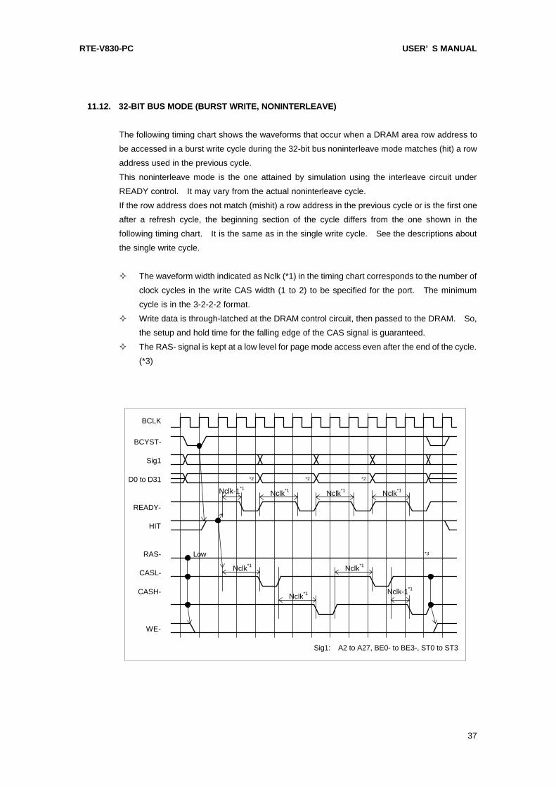
11.12. 32-BIT BUS MODE (BURST WRITE, NONINTERLEAVE)
The following timing chart shows the waveforms that occur when a DRAM area row address to
be accessed in a burst write cycle during the 32-bit bus noninterleave mode matches (hit) a row
address used in the previous cycle.
This noninterleave mode is the one attained by simulation using the interleave circuit under
READY control. It may vary from the actual noninterleave cycle.
If the row address does not match (mishit) a row address in the previous cycle or is the first one
after a refresh cycle, the beginning section of the cycle differs from the one shown in the
following timing chart. It is the same as in the single write cycle. See the descriptions about
the single write cycle.
² The waveform width indicated as Nclk (*1) in the timing chart corresponds to the number of
clock cycles in the write CAS width (1 to 2) to be specified for the port. The minimum
cycle is in the 3-2-2-2 format.
² Write data is through-latched at the DRAM control circuit, then passed to the DRAM. So,
the setup and hold time for the falling edge of the CAS signal is guaranteed.
² The RAS- signal is kept at a low level for page mode access even after the end of the cycle.
(*3)
WE-
CASH-
CASL-
*2
*3
Nclk*1Nclk-1*1
Nclk*1
Low
HIT
RAS-
Sig1: A2 to A27, BE0- to BE3-, ST0 to ST3
Sig1
D0 to D31
READY-
BCYST-
BCLK
*2
Nclk*1
*2
Nclk*1
Nclk*1
Nclk*1
Nclk-1*1

RTE-V830-PC USER’ S MANUAL
38
11.13. 16-BIT BUS MODE (SINGLE READ)
The byte-unit or halfword-unit single read access in the 16-bit bus mode is the same as that in
the 32-bit bus mode. The word-unit single read access in the 16-bit bus mode behaves
similarly to the burst mode, and differs from that in the 32-bit bus mode.
The following timing charts show the waveforms that occur when a row address in a word-unit
single read cycle during the 16-bit bus mode matches (hit) a row address in the previous cycle.
The first timing chart applies to the interleave mode, while the second timing chart applies to the
noninterleave mode.
For a row address that does not match the one in the previous cycle (mishit) or for the first cycle
after a refresh cycle, the single read cycle in the 16-bit bus mode is the same as that in the 32-
bit bus mode. See the descriptions about the single read cycle in the 32-bit bus mode.
² The waveform width indicated as Nclk (*1) in the timing chart corresponds to the number of
clock cycles in the read CAS width (1 to 3) to be specified for the port. The minimum
cycle is in the 3-1 format for the interleave mode and the 3-2 format for the noninterleave
mode.
² The RAS- signal is kept at a low level for page mode access even after the end of the cycle.
(*2)
² The upper and lower 32-bit banks are read simultaneously. The CPU is supplied with the
lower and upper 16 bits from an appropriate bank according to the state of A1 in the stated
order.
WE-
CASH-
CASL-
*2Low
Nclk*1
RAS-
Sig1: A2 to A27, BE0- to BE3-, ST0 to ST3
D0 to D15
Sig1
READY-
BCYST-
BCLK
HIT

RTE-V830-PC USER’ S MANUAL
39
WE-
CASH-
CASL-
*2Low
Nclk*1
RAS-
Sig1: A2 to A27, BE0- to BE3-, ST0 to ST3
D0 to D15
Sig1
READY-
BCYST-
BCLK
HIT
Nclk*1

RTE-V830-PC USER’ S MANUAL
40
11.14. 16-BIT BUS MODE (SINGLE WRITE)
The byte-unit or halfword-unit single write access in the 16-bit bus mode is the same as that in
the 32-bit bus mode. The word-unit single write access in the 16-bit bus mode behaves
similarly to the burst mode, and differs from that in the 32-bit bus mode.
The following timing chart shows the waveforms that occur when a row address in a word-unit
single write cycle during the 16-bit bus mode matches (hit) a row address used in the previous
cycle. This timing chart applies to both the interleave and noninterleave modes.
For a row address that does not match the one in the previous cycle (mishit) or for the first cycle
after a refresh cycle, the single write cycle in the 16-bit bus mode is the same as that in the
32-bit bus mode. See the descriptions about the single write cycle in the 32-bit bus mode.
² The waveform width indicated as Nclk (*1) in the timing chart corresponds to the number of
clock cycles in the write CAS width (1 or 2) to be specified for the port. The minimum
cycle is in the 2-2 format.
² The RAS- signal is kept at a low level for page mode access even after the end of the cycle.
(*2)
² The CASL- and CASH- signal, whichever corresponds to the appropriate byte position in
the appropriate bank, becomes active according to the state of A2 and bus enable signals
BE0- to BE3-. (*3)
² Write data in the first cycle is through-latched at the DRAM control circuit so that it can be
written on a single CAS signal.
WE-
CASH-
CASL-
*4
*3
*3
*2Low
Nclk*1
Nclk*1
RAS-
Sig1: A2 to A27, BE0- to BE3-, ST0 to ST3
D0 to D15
Sig1
READY-
BCYST-
BCLK
HIT
Nclk*1
Nclk*1

RTE-V830-PC USER’ S MANUAL
41
11.15. 16-BIT BUS MODE (BURST READ, INTERLEAVE)
The following timing chart shows the waveforms that occur when a DRAM area row address to
be accessed in a burst read cycle during the 16-bit bus interleave mode matches (hit) a row
address used in the previous cycle.
If the row address does not match (mishit) a row address used in the previous cycle or is the first
one after a refresh cycle, only the beginning section of the cycle differs from the one in the 32-
bit bus mode. See the descriptions about the single read cycle in the 32-bit bus mode.
² The waveform width indicated as Nclk (*1) in the timing chart corresponds to the number of
clock cycles in the read CAS width (1 to 3) to be specified for the port. The minimum
cycle is in the 3-1-1-1-1-1-1-1 format.
² 64 bits of data are read at a time. Groups of 16 bits are passed to the CPU sequentially
starting at the lowest group. (*2)
² The RAS- signal is kept at a low level for page mode access even after the end of the cycle.
(*3)
WE-
CASH-
CASL-
*2*2*2*2*2*2*2*2
*3Low
Nclk*1
RAS-
Sig1: A2 to A27, BE0- to BE3-, ST0 to ST3
D0 to D15
Sig1
READY-
BCYST-
BCLK
HIT
Nclk*1
Nclk-1*1Nclk-1*1

RTE-V830-PC USER’ S MANUAL
42
11.16. 16-BIT BUS MODE (BURST WRITE, INTERLEAVE)
The following timing chart shows the waveforms that occur when a DRAM area row address to
be accessed in a burst write cycle during the 16-bit bus interleave mode matches (hit) a row
address used in the previous cycle.
If the row address does not match (mishit) a row address used in the previous cycle or is the first
one after a refresh cycle, only the beginning section of the cycle differs from that in the 32-bit bus
mode. See the descriptions about the single write cycle in the 32-bit bus mode.
² The waveform width indicated as Nclk (*1) in the timing chart corresponds to the number of
clock cycles in the write CAS width (1 or 2) to be specified for the port. The minimum
cycle is in the 3-1-1-1-1-1-1-2 format.
² Write data is through-latched at the DRAM control circuit, then passed to the DRAM. So,
the setup and hold time for the falling edge of the CAS signal is guaranteed.
² The RAS- signal is kept at a low level for page mode access even after the end of the cycle.
(*3)
WE-
CASH-
CASL-
*2*2
*3LowRAS-
Sig1: A2 to A27, BE0- to BE3-, ST0 to ST3
D0 to D15
Sig1
READY-
BCYST-
BCLK
HIT
Nclk-1*1 Nclk-1*1 Nclk-1*1
*2*2
Nclk-1*1 Nclk-1*1 Nclk*1Nclk-1*1
*2*2 *2*2

RTE-V830-PC USER’ S MANUAL
43
11.17. 16-BIT BUS MODE (BURST READ, NONINTERLEAVE)
The following timing chart shows the waveforms that occur when a DRAM area row address to
be accessed in a burst read cycle during the 16-bit bus noninterleave mode matches (hit) a row
address used in the previous cycle.
This noninterleave mode is the one attained by simulation using the interleave circuit under
READY control. It may vary from the actual noninterleave cycle.
If the row address does not match (mishit) a row address used in the previous cycle or is the first
one after a refresh cycle, only the beginning section of the cycle differs from that in the 32-bit bus
mode. See the descriptions about the single read cycle in the 32-bit bus mode.
² The waveform width indicated as Nclk (*1) in the timing chart corresponds to the number of
clock cycles in the read CAS width (1 to 3) to be specified for the port. The minimum
cycle is in the 3-2-2-2-2-2-2-2 format.
² 64 bits of data are read at a time. Groups of 16 bits are passed to the CPU sequentially
starting at the lowest group.
² The RAS- signal is kept at a low level for page mode access even after the end of the cycle.
(*3)
WE-
CASH-
CASL-
*2
Low
Nclk*1
Nclk*1
RAS-
Sig1: A2 to A27, BE0- to BE3-, ST0 to ST3
D0 to D15
Sig1
READY-
BCYST-
BCLK
*2*2*2*2
HIT
*2*2*2
*3
Nclk-1*1
Nclk*1
Nclk*1 Nclk*1Nclk*1 Nclk*1Nclk*1 Nclk*1

RTE-V830-PC USER’ S MANUAL
44
11.18. 16-BIT BUS MODE (BURST WRITE, NONINTERLEAVE)
The following timing chart shows the waveforms that occur when a DRAM area row address to
be accessed in a burst write cycle during the 16-bit bus noninterleave mode matches (hit) a row
address used in the previous cycle.
This noninterleave mode is the one attained by simulation using the interleave circuit under
READY control. It may vary from the actual noninterleave cycle.
If the row address does not match (mishit) a row address used in the previous cycle or is the first
one after a refresh cycle, only the beginning section of the cycle differs from that in the 32-bit bus
mode. See the descriptions about the single write cycle in the 32-bit bus mode.
² The waveform width indicated as Nclk (*1) in the timing chart corresponds to the number of
clock cycles in the write CAS width (1 or 2) to be specified for the port. The minimum
cycle is in the 3-2-2-2-2-2-2-2 format.
² Write data is through-latched at the DRAM control circuit, then passed to the DRAM. So,
the setup and hold time for the falling edge of the CAS signal is guaranteed. (*2)
² The RAS- signal is kept at a low level for page mode access even after the end of the cycle.
(*3)
WE-
CASH-
CASL-
*2*2
*3LowRAS-
Sig1: A2 to A27, BE0- to BE3-, ST0 to ST3
D0 to D15
Sig1
READY-
BCYST-
BCLK
HIT
Nclk*1 Nclk*1 Nclk*1
*2*2
Nclk*1 Nclk*1 Nclk*1Nclk*1
*2*2 *2*2

RTE-V830-PC USER’ S MANUAL
45
- Memo -
RTE-V830-PC User’ s Manual M471MNL02
Midas lab