Embed Size (px)
Citation preview
RS FLIP FLOP BASIC OPERATION
INEL 4207 Digital Electronics - M. Toledo
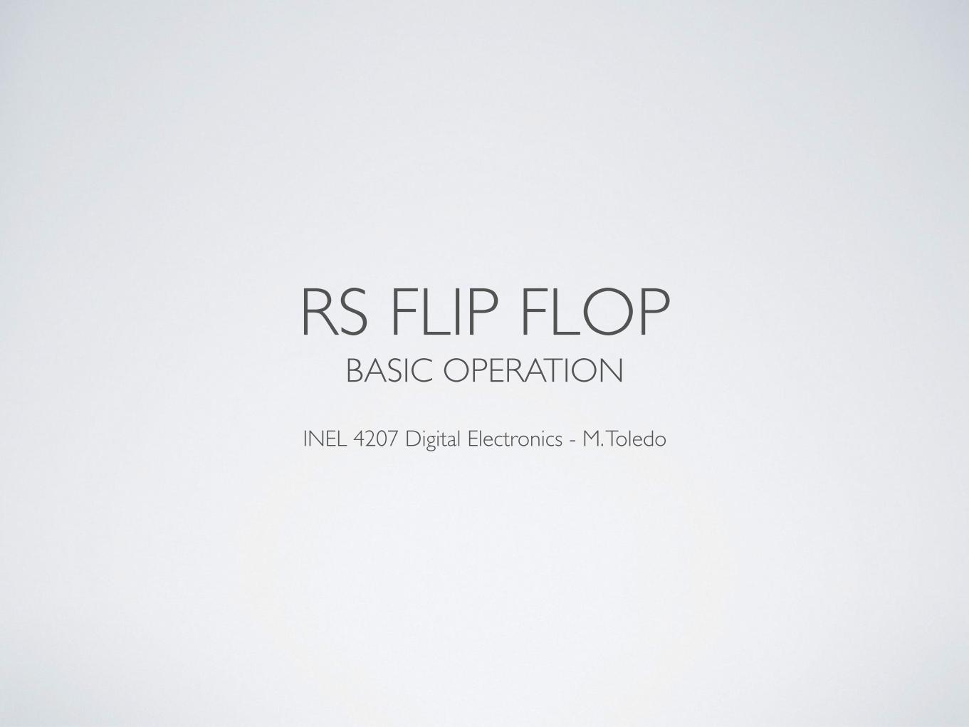
Figure 16.11 A 2M+N -bit memory chip organized as an array of 2M rows × 2N columns.
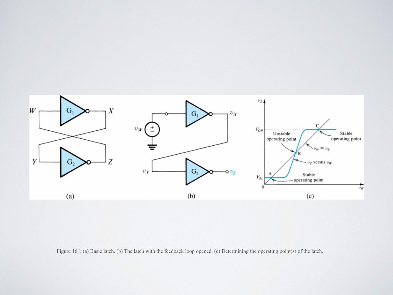
Figure 16.1 (a) Basic latch. (b) The latch with the feedback loop opened. (c) Determining the operating point(s) of the latch.
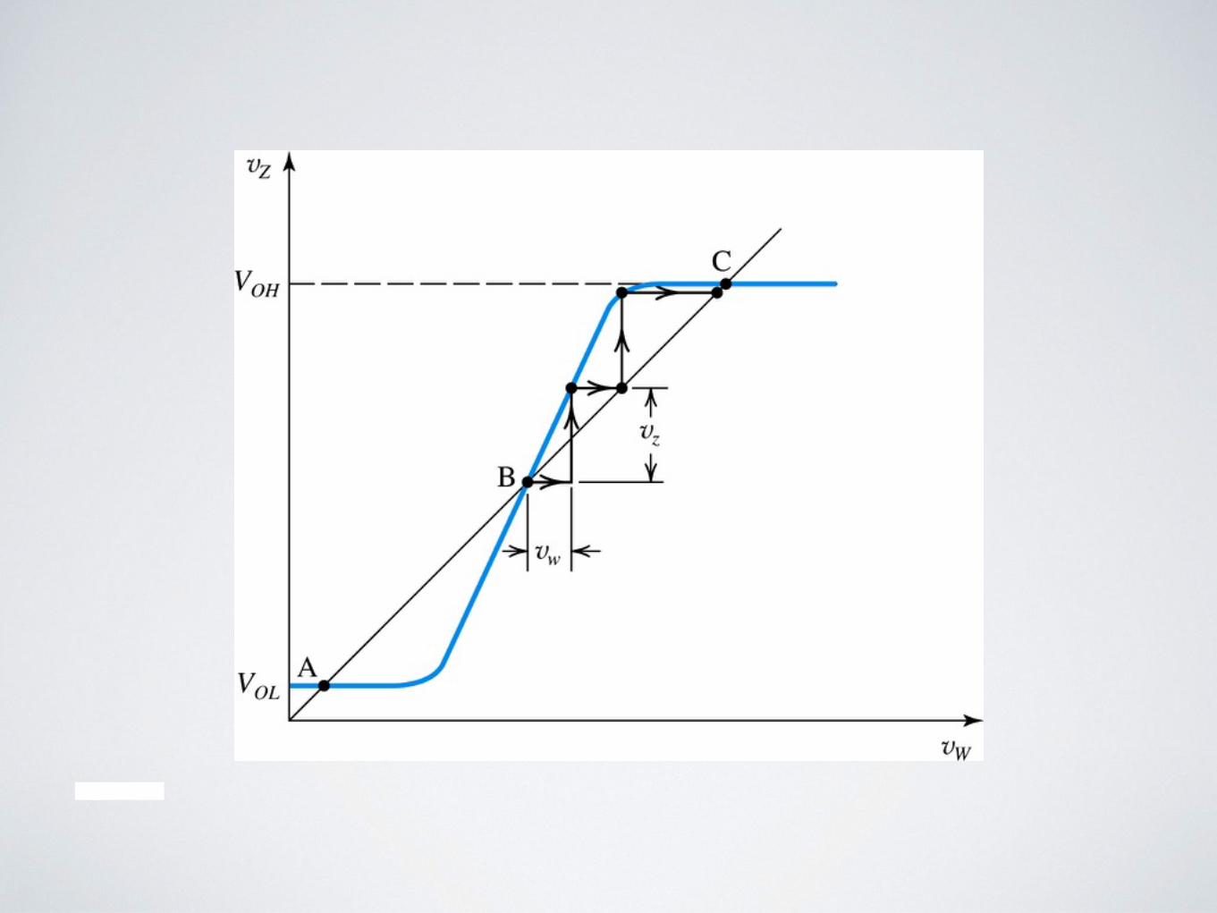
Figure 16.2
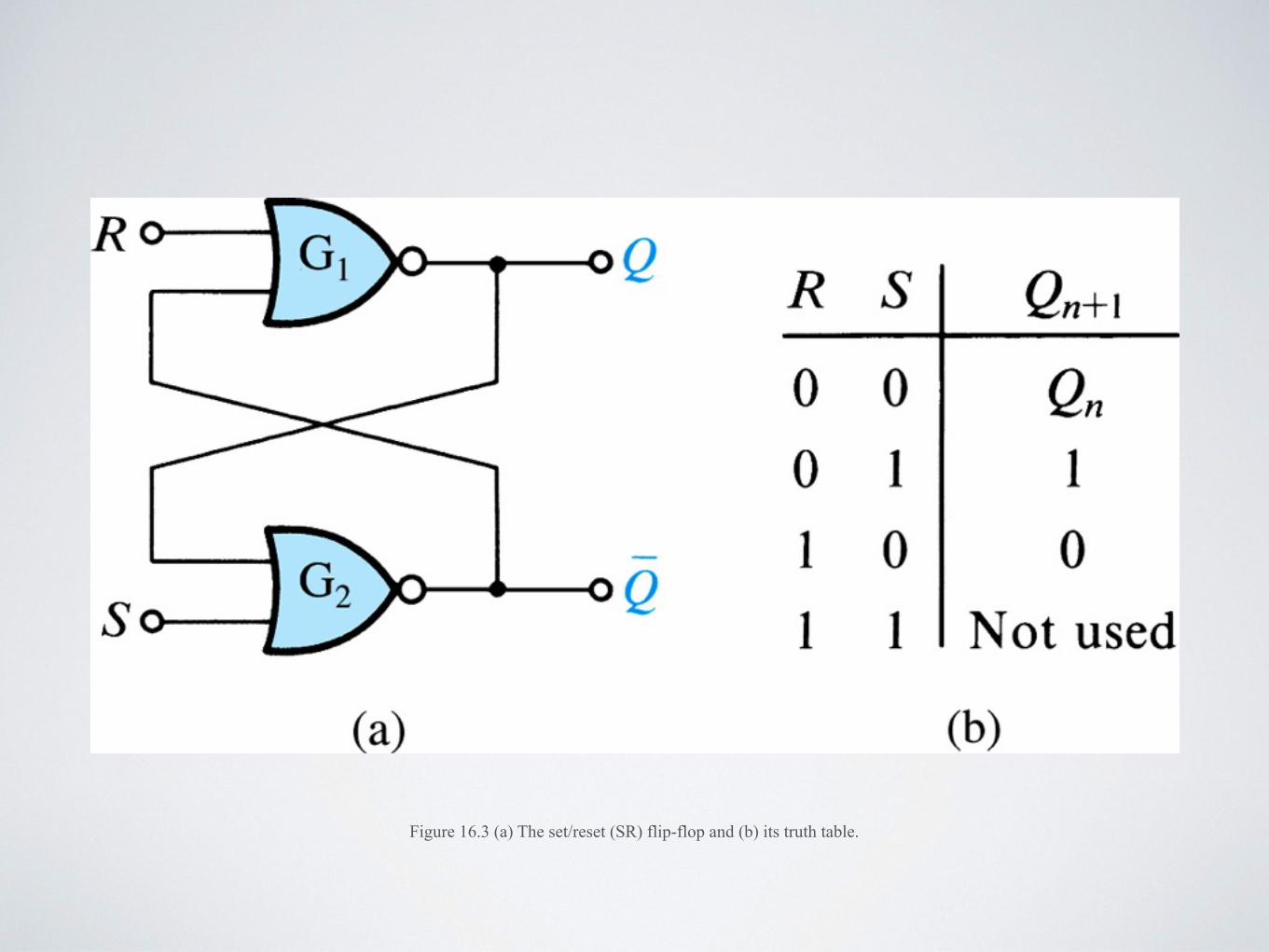
Figure 16.3 (a) The set/reset (SR) flip-flop and (b) its truth table.
-
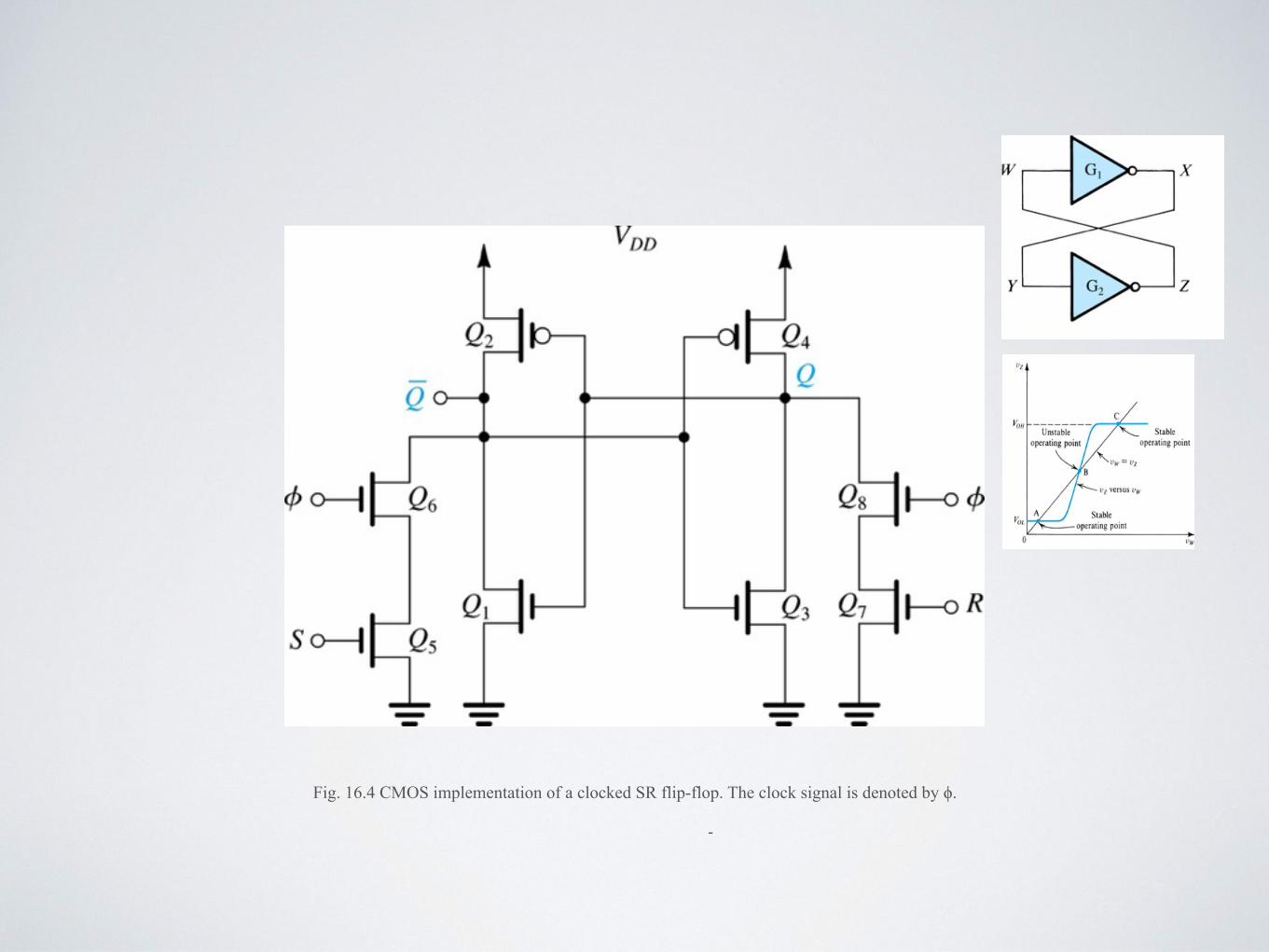
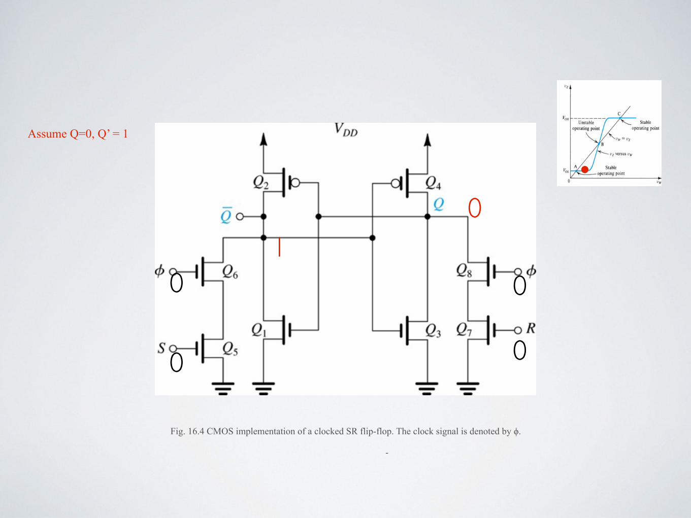
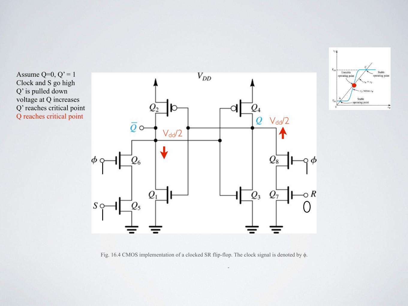
Fig. 16.4 CMOS implementation of a clocked SR flip-flop. The clock signal is denoted by ϕ.
-
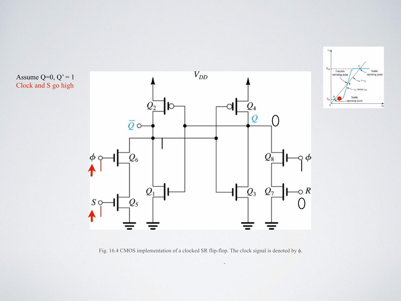
Fig. 16.4 CMOS implementation of a clocked SR flip-flop. The clock signal is denoted by ϕ.
01
Assume Q=0, Q’ = 1
0
0
0
0
⦁
-
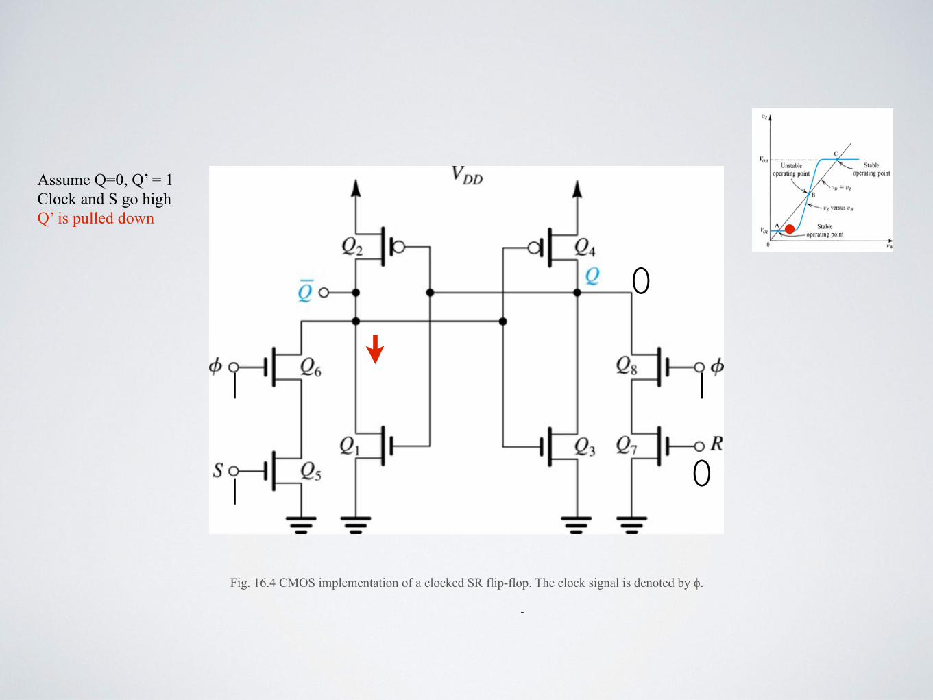
Fig. 16.4 CMOS implementation of a clocked SR flip-flop. The clock signal is denoted by ϕ.
01
Assume Q=0, Q’ = 1 Clock and S go high
1
1
1
0
⦁
-
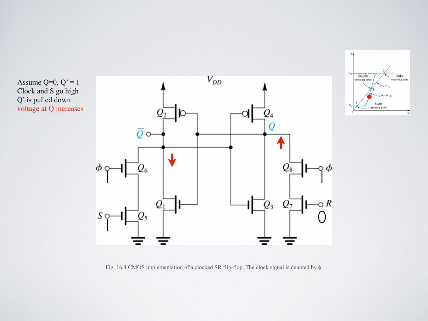
Fig. 16.4 CMOS implementation of a clocked SR flip-flop. The clock signal is denoted by ϕ.
0
Assume Q=0, Q’ = 1 Clock and S go high Q’ is pulled down
1
1
1
0
⦁
-
Fig. 16.4 CMOS implementation of a clocked SR flip-flop. The clock signal is denoted by ϕ.
Assume Q=0, Q’ = 1 Clock and S go high Q’ is pulled down voltage at Q increases
1
1
1
0
⦁

-
Fig. 16.4 CMOS implementation of a clocked SR flip-flop. The clock signal is denoted by ϕ.
Assume Q=0, Q’ = 1 Clock and S go high Q’ is pulled down voltage at Q increases Q’ reaches critical point
1
1
Vdd/2
1
0
⦁
-
Fig. 16.4 CMOS implementation of a clocked SR flip-flop. The clock signal is denoted by ϕ.
Assume Q=0, Q’ = 1 Clock and S go high Q’ is pulled down voltage at Q increases Q’ reaches critical point Q reaches critical point
1
1
Vdd/2Vdd/2
1
0
⦁
-
Fig. 16.4 CMOS implementation of a clocked SR flip-flop. The clock signal is denoted by ϕ.
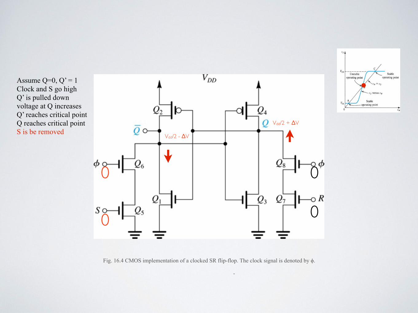
Assume Q=0, Q’ = 1 Clock and S go high Q’ is pulled down voltage at Q increases Q’ reaches critical point Q reaches critical point S is be removed
0
0
Vdd/2 - ΔV
Vdd/2 + ΔV
0
0
⦁
-
Fig. 16.4 CMOS implementation of a clocked SR flip-flop. The clock signal is denoted by ϕ.
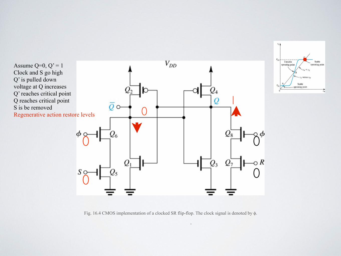
Assume Q=0, Q’ = 1 Clock and S go high Q’ is pulled down voltage at Q increases Q’ reaches critical point Q reaches critical point S is be removed Regenerative action restore levels
0
0
01
0
0
⦁
-
Fig. 16.4 CMOS implementation of a clocked SR flip-flop. The clock signal is denoted by ϕ.
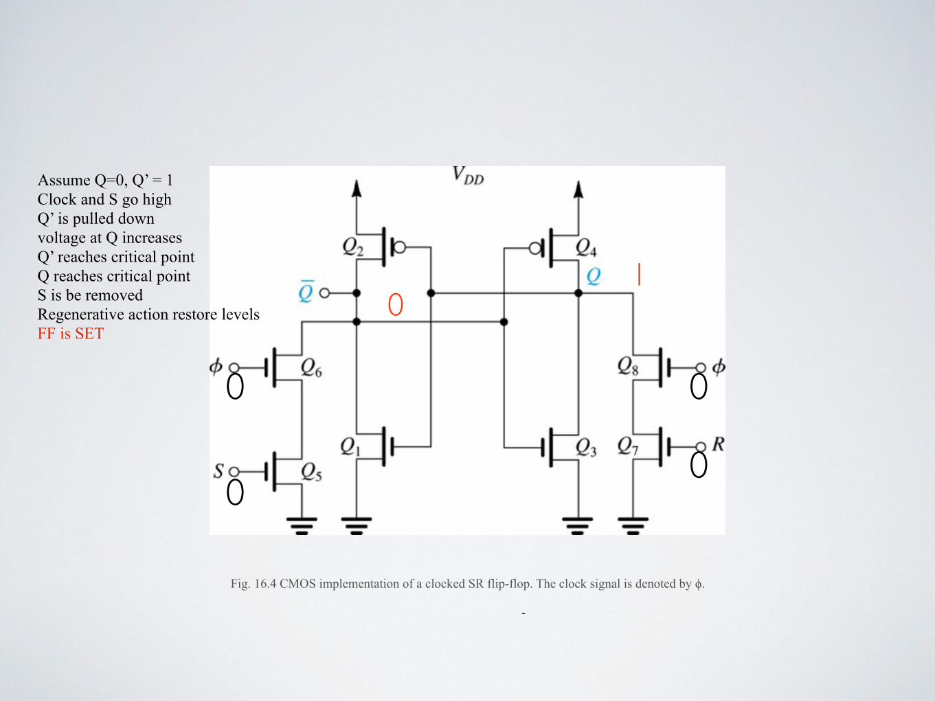
Assume Q=0, Q’ = 1 Clock and S go high Q’ is pulled down voltage at Q increases Q’ reaches critical point Q reaches critical point S is be removed Regenerative action restore levels FF is SET
0
0
01
0
0
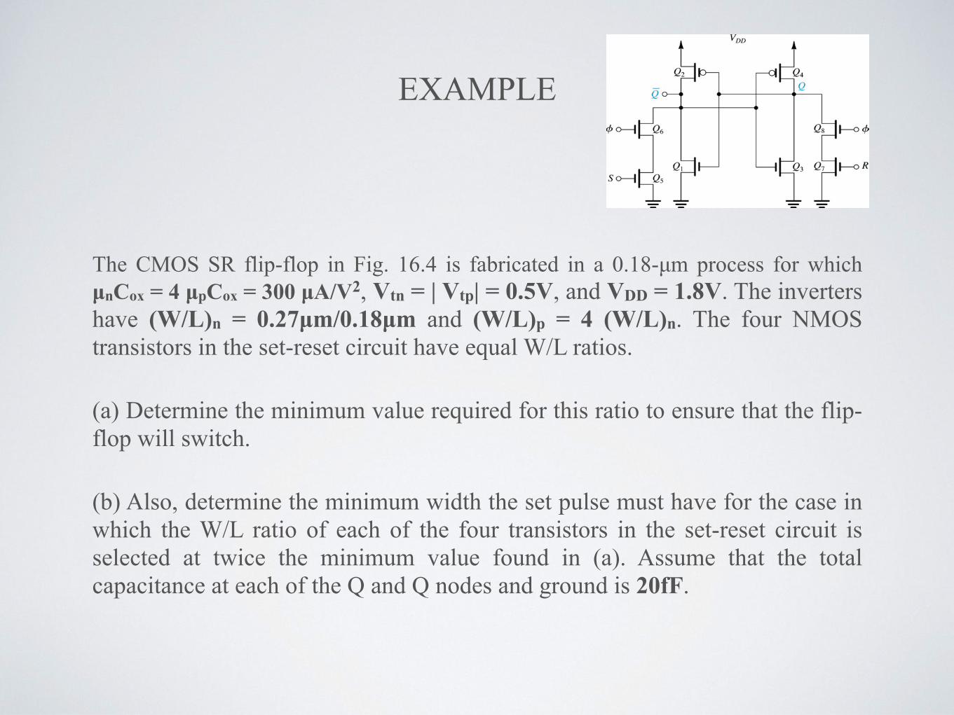
EXAMPLE
The CMOS SR flip-flop in Fig. 16.4 is fabricated in a 0.18-µm process for which µnCox = 4 µpCox = 300 µA/V2, Vtn = | Vtp| = 0.5V, and VDD = 1.8V. The inverters have (W/L)n = 0.27µm/0.18µm and (W/L)p = 4 (W/L)n. The four NMOS transistors in the set-reset circuit have equal W/L ratios.
(a) Determine the minimum value required for this ratio to ensure that the flip-flop will switch.
(b) Also, determine the minimum width the set pulse must have for the case in which the W/L ratio of each of the four transistors in the set-reset circuit is selected at twice the minimum value found in (a). Assume that the total capacitance at each of the Q and Q nodes and ground is 20fF.
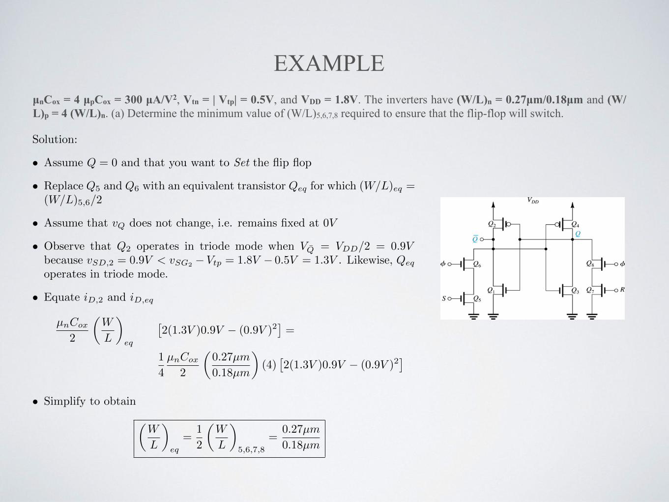
EXAMPLEµnCox = 4 µpCox = 300 µA/V2, Vtn = | Vtp| = 0.5V, and VDD = 1.8V. The inverters have (W/L)n = 0.27µm/0.18µm and (W/L)p = 4 (W/L)n. (a) Determine the minimum value of (W/L)5,6,7,8 required to ensure that the flip-flop will switch.
Solution:
• Assume Q = 0 and that you want to Set the flip flop
• Replace Q5 and Q6 with an equivalent transistor Qeq
for which (W/L)eq
=(W/L)5,6/2
• Assume that vQ
does not change, i.e. remains fixed at 0V
• Observe that Q2 operates in triode mode when VQ̄
= VDD
/2 = 0.9Vbecause v
SD,2 = 0.9V < vSG2 � V
tp
= 1.8V � 0.5V = 1.3V . Likewise, Qeq
operates in triode mode.
• Equate iD,2 and i
D,eq
µn
Cox
2
✓W
L
◆
eq
⇥2(1.3V )0.9V � (0.9V )2
⇤=
1
4
µn
Cox
2
✓0.27µm
0.18µm
◆(4)
⇥2(1.3V )0.9V � (0.9V )2
⇤
• Simplify to obtain
✓W
L
◆
eq
=1
2
✓W
L
◆
5,6,7,8
=0.27µm
0.18µm
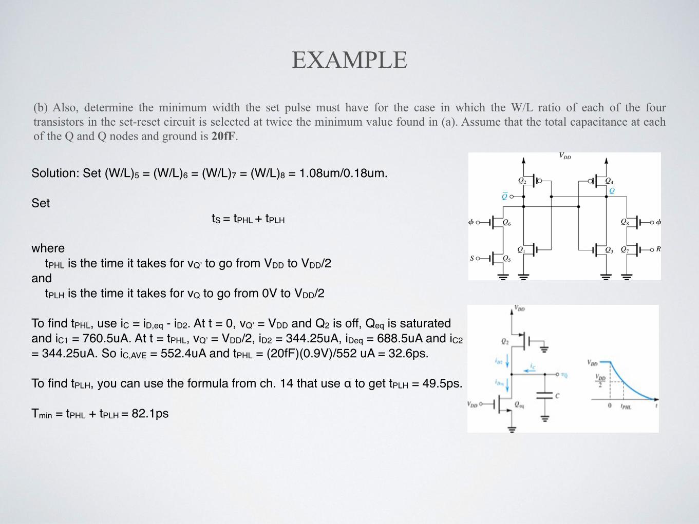
EXAMPLE
(b) Also, determine the minimum width the set pulse must have for the case in which the W/L ratio of each of the four transistors in the set-reset circuit is selected at twice the minimum value found in (a). Assume that the total capacitance at each of the Q and Q nodes and ground is 20fF.
Solution: Set (W/L)5 = (W/L)6 = (W/L)7 = (W/L)8 = 1.08um/0.18um.
Set tS = tPHL + tPLH
where tPHL is the time it takes for vQ’ to go from VDD to VDD/2
and tPLH is the time it takes for vQ to go from 0V to VDD/2
To find tPHL, use iC = iD,eq - iD2. At t = 0, vQ’ = VDD and Q2 is off, Qeq is saturated and iC1 = 760.5uA. At t = tPHL, vQ’ = VDD/2, iD2 = 344.25uA, iDeq = 688.5uA and iC2 = 344.25uA. So iC,AVE = 552.4uA and tPHL = (20fF)(0.9V)/552 uA = 32.6ps.
To find tPLH, you can use the formula from ch. 14 that use α to get tPLH = 49.5ps.
Tmin = tPHL + tPLH = 82.1ps
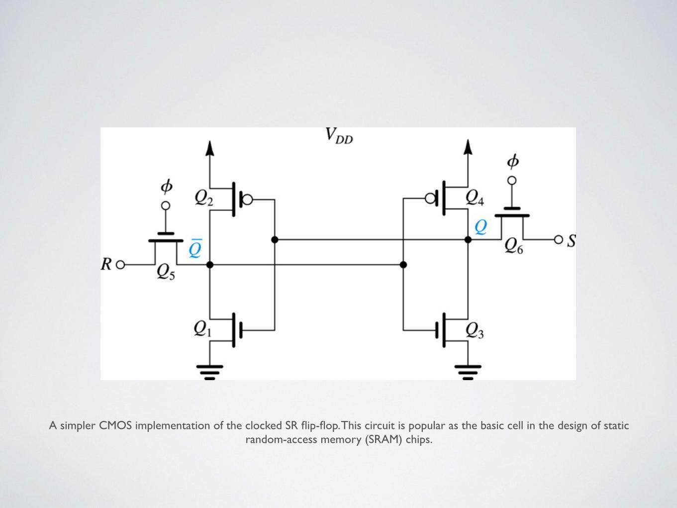
A simpler CMOS implementation of the clocked SR flip-flop. This circuit is popular as the basic cell in the design of static random-access memory (SRAM) chips.
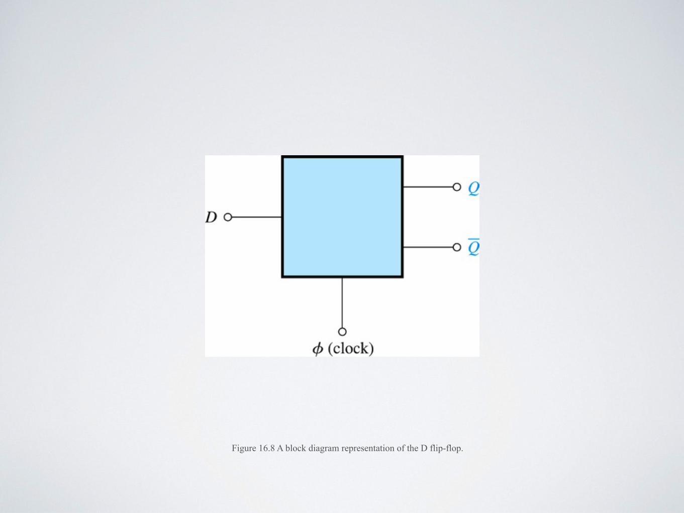
Figure 16.8 A block diagram representation of the D flip-flop.
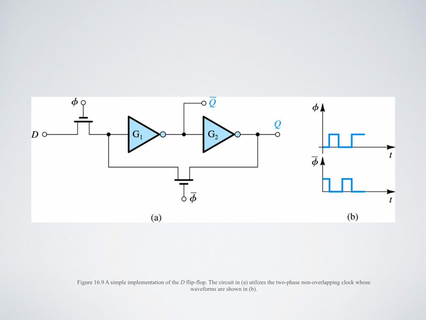
Figure 16.9 A simple implementation of the D flip-flop. The circuit in (a) utilizes the two-phase non-overlapping clock whose waveforms are shown in (b).
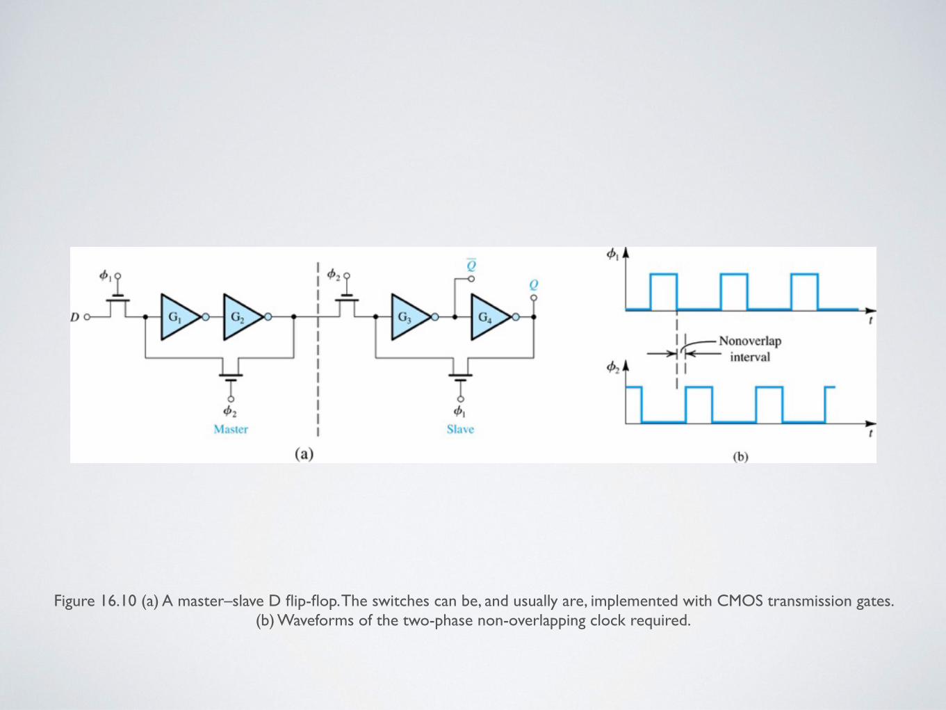
Figure 16.10 (a) A master–slave D flip-flop. The switches can be, and usually are, implemented with CMOS transmission gates. (b) Waveforms of the two-phase non-overlapping clock required.