Embed Size (px)
Citation preview

RPC-320 USER'S MANUAL REV 2
Page i RPC -320
Copyright 1997, 1999 - Remote Processing C orporation.
All rights reserved. However, any part of this document
may be reproduc ed with Remote Proce ssing cited as the
source.
The con tents of this ma nual and the sp ecifications her ein
may change without notice.
TRADEMARKS
RPBASIC-52™ is a trademark of Remote P rocessing
Corpor ation.
PC SmartLINK® is a trademark of Octagon Systems
Corpor ation.
BASIC-52© is a trademark of Intel Corpor ation.
Remote Processing Corporation
79 75 E. Harvard Ave.
Denver, Co 802 31 USA
T el: (3 0 3 ) 6 9 0 - 1 5 8 8
Fa x: (3 0 3 ) 6 9 0 - 1 8 7 5
w w w .rp3 .com
NOTICE TO USER
The information contained in this manual is believed
correct. However, Remote Pr ocessing assumes no
responsibility for any of the circuits described herein,
conveys no license under any patent or other right, and
make no repre sentations that the circuits are free from
patent infringement. Rem ote Processing makes no
representation or warr anty that such applications will be
suitable for the use specified without further testing or
modification. The user must make the final
determination as to fitness for a particular use.
Remote Pr ocessing Corporation' s general policy does not
recommend the use of its products in life support
applications where the failure or malfunction of a
component m ay directly threaten life or injury. It is a
Condition of Sale that the user of Remote Processing
products in life support applications assum es all the risk
of such use and indemn ifies Remote Pr ocessing against
all damages.
P/N 1366
Revision: 2.8

TABLE OF CONTENTS
Page ii RPC-320
SECTION 1 OVERVIEW
DESCRIPTION . . . . . . . . . . . . . . . . . . . 1-1
MANUAL ORGANIZATION . . . . . . . . . . 1-1
MANUAL CONVENTIONS . . . . . . . . . . . 1-1
Symbols and Term inology . . . . . . . . . 1-2
TECHNICA L SUPPORT . . . . . . . . . . . . . 1-2
SECTION 2 SETUP AND OPERATION
INTRODUCTION . . . . . . . . . . . . . . . . . 2-1
OPERATING PRECAUTIONS . . . . . . . . . 2-1
EQUIPMENT . . . . . . . . . . . . . . . . . . . . 2-1
FIRST TIME OPERATION . . . . . . . . . . . 2-2
Using a PC . . . . . . . . . . . . . . . . . . . 2-2
Using a Terminal . . . . . . . . . . . . . . . 2-2
UPLOADING AND DOWNLOADING
PROGRAMS . . . . . . . . . . . . . . . . . 2-2
Editing pr ogram s and pro gram ming hints 2-3
WHERE TO G O FROM H ERE . . . . . . . . . 2-4
TROUBLESHOOTING . . . . . . . . . . . . . . 2-4
SECTION 3 SAVING PROGRAMS
INTRODUCTION . . . . . . . . . . . . . . . . . 3-1
SAVING A PROGRAM . . . . . . . . . . . . . 3-1
AUTORUNNING . . . . . . . . . . . . . . . . . . 3-2
PREVENTING AUTORUN . . . . . . . . . . . 3-2
LOADING A PROGRAM . . . . . . . . . . . . 3-2
CHANGING EPROM SIZE . . . . . . . . . . . 3-2
ALTERNATE EPROMS . . . . . . . . . . . . . 3-3
COMMANDS . . . . . . . . . . . . . . . . . . . . 3-3
SECTION 4 SERIAL PORTS
DESCRIPTION . . . . . . . . . . . . . . . . . . . 4-1
COM0 SERIAL PORT . . . . . . . . . . . . . . 4-1
COM1 SERIAL PORT . . . . . . . . . . . . . . 4-1
RS-422/485 OPERATING INFORMATION . 4-2
RS-422/485 Termination network . . . . . 4-2
Two wire RS-485 . . . . . . . . . . . . . . . 4-3
Multidrop Network . . . . . . . . . . . . . . 4-3
ACCESSING SERIAL BUFFERS . . . . . . . 4-3
ACCESSING COM0 AND COM1 . . . . . . . 4-4
DISABLIN G CON TROL -C . . . . . . . . . . . 4-4
SERIAL PORT PIN OUT . . . . . . . . . . . . 4-4
SECTION 5 RAM ME MORY
INTRODUCTION . . . . . . . . . . . . . . . . . 5-1
CHANGING M EMORY . . . . . . . . . . . . . 5-1
BATTERY BACKUP . . . . . . . . . . . . . . . 5-1
Checking the battery . . . . . . . . . . . . . 5-1
RESERVED ME MORY . . . . . . . . . . . . . 5-2
STORING VARIABLES IN RAM . . . . . . . 5-2
BLOCK DATA TRANSFER . . . . . . . . . . . 5-3
ASSEMBLY LANGUAGE INTERFACE . . 5-3
COMMANDS . . . . . . . . . . . . . . . . . . . . 5-3
SECTION 6 DIGITAL AND OPTO PORTS
INTRODUCTION . . . . . . . . . . . . . . . . . 6-1
DIGITAL I/O PORTS . . . . . . . . . . . . . . . 6-1
Digital Port J3 . . . . . . . . . . . . . . . . . 6-1
Digital Port P6 . . . . . . . . . . . . . . . . . 6-2
High Current Port L8 . . . . . . . . . . . . 6-2
Optically Isolated Input . . . . . . . . . . . 6-2
Digital I/O Com mands . . . . . . . . . . . . 6-2
High Curr ent Output . . . . . . . . . . . . . 6-3
Interfac ing Digital I/ O to an opto- module
rack . . . . . . . . . . . . . . . . . . . . . 6-4
Interfacing to switches and other devices 6-4
Digital I/ O pro gram ming exa mple . . . . 6-4
Pulse Width Modulat ion (PWM) . . . . . . 6-5
COMMANDS . . . . . . . . . . . . . . . . . . . . 6-6
SECTION 7 CALENDAR/CLOCK
DESCRIPTION . . . . . . . . . . . . . . . . . . . 7-1
SETTING DATE AND TIME . . . . . . . . . . 7-1
COMMANDS . . . . . . . . . . . . . . . . . . . . 7-1
SECTION 8 DISPLAY PORT
INTRODUCTION . . . . . . . . . . . . . . . . . 8-1
CONNECTING DISPLAYS . . . . . . . . . . . 8-1
WRITING TO THE DISPLAY . . . . . . . . . 8-1
PROGRAMMING EXAMPLE . . . . . . . . . 8-1
DISPLAY TYPES . . . . . . . . . . . . . . . . . 8-2
DISPLAY CONNECTOR PIN OUT . . . . . 8-2
COMMANDS . . . . . . . . . . . . . . . . . . . . 8-2
SECTION 9 KEYPAD PORT
INTRODUCTION . . . . . . . . . . . . . . . . . 9-1
PROGRAMMING EXAMPLE . . . . . . . . . 9-1
KEYP AD P ORT P IN OU T - J5 . . . . . . . . . 9-2
SECT ION 10 ANALOG INPUT
DESCRIPTION . . . . . . . . . . . . . . . . . . . 10-1
CONNECTING ANALOG INPUTS . . . . . . 10-1
Overvoltage conditions . . . . . . . . . . . . 10-1
Grounding . . . . . . . . . . . . . . . . . . . . 10-1
INITIALIZATION . . . . . . . . . . . . . . . . . 10-1
Differential Mode . . . . . . . . . . . . . . . 10-2
Examples using CON FIG AIN . . . . . . . 10-2
Acquir ing Analog Data . . . . . . . . . . . . . . 10-2
Noise Notes . . . . . . . . . . . . . . . . . . . 10-3
Temper ature Measur ement . . . . . . . . . 10-3
Data logging on a timer tick . . . . . . . . 10-4
MEASURING HIGHER VOLTAGES . . . . 10-4
CONVERTING ANALOG MEASUREMENTS 10-4
Measuring 4-20 mA current loops . . . . . 10-4
AMPLIFIERS . . . . . . . . . . . . . . . . . . . . 10-5
CALIBRATION . . . . . . . . . . . . . . . . . . 10-5
COMMANDS . . . . . . . . . . . . . . . . . . . . 10-5

TABLE OF CONTENTS
Page iii RPC-320
SECT ION 11 WATCHDOG TIMER
DESCRIPTION . . . . . . . . . . . . . . . . . . . 11-1
EXTERNAL RESET . . . . . . . . . . . . . . . . 11-1
DESCRIPTION . . . . . . . . . . . . . . . . . . . 11-1
OPTICALLY ISOLATED INTERRUPT . . . 11-1
INTERRUPT CHARACTERISTICS . . . . . . 11-1
SECT ION 12 EXTERNAL INTERRUPT
DESCRIPTION . . . . . . . . . . . . . . . . . . . 12-1
PROGRAMMING . . . . . . . . . . . . . . . . . 12-1
Program exam ples . . . . . . . . . . . . . . 12-1
COMMANDS . . . . . . . . . . . . . . . . . . . . 12-2
SECT ION 13 MULTI-MODE COUNTER
DESCRIPTION . . . . . . . . . . . . . . . . . . . 13-1
SECT ION 14 POWER REDUCTION
FURTHER POWER REDUCTION . . . . . . 14-1
Prog ram Exam ple . . . . . . . . . . . . . . . 14-2
SECT ION 15 TECHNICAL INFORMATION
ELECTRICAL SPECIFICATIONS . . . . . . 15-1
MEMORY AND I/O BANK MAP . . . . . . . 15-2
MECHANICAL SPECIFICATIONS . . . . . 15-2
JUMPER DESCRIPTIONS . . . . . . . . . . . 15-2

SOFTWARE REVISION HISTORY
Page iv RPC -320
V1.04 Release for RPC 320
V1.05 BSAVE retur ned a hardware er ror when ver ify
was bad. In fact, save was OK.
V1.06 LCD graphics hardware CS and reset are
reversed. C ompensated in software.
V1.07 MTO P was useless in any system, especially a
32K RAM.
V1.08 Varia bles E and F wo uld get dro pped if
followed by a space.
Added de lays betwee n data strob e writes to
LCD display.
V1.09 STR(7, . . .) did not put in a CR into the put
string, causing longer strings to be printed.
V1.10 Initial release for RPC-330.
Added AOT command (330 only)
Added COUNT, ON COM , ON COUNT, ON
LINE, and ON KEYPAD
V1.11 11/29/95
Added day of week to DAT E comm and and
function.
V1.12 12/01/95
Added code to use Atmel 29C040A flash.
V1.13 01/12/96
Added code to support IEE centry series
display (3602-100-05420)
Includes PRINT #port
V1.14 03/28/96
Fixed bug in ON C OUN T. Returns error for
lines > 100.
V1.15 06/26/96
PEEK$ could cause BASIC to lock up under
right conditions.
V1.16 02/18/97
ON LIN E OF F could cause program to lock up
if running ON COM.
Syntax error when DISPLAY used with IF-
THEN-ELSE.
Added PE EKF a nd POKE F com mands.

OVERVIEW SECTION 1
Page 1-1 RPC -320
DESCRIPTION
The RP C-320 is a n embed ded contr oller with a built in
Basic language. Several featur es make it suitable as a
stand alone un it:
Built in RPBASIC-52 programm ing language
supports hardware using single commands. On card
flash EPROM programm er can save up to 8
progr ams to 62K , or about 500K tota l.
High speed multimode counter accepts quadrature or
single inputs. Program mable for up/dow n, binary,
divide-by-N, X1, X2 or X4 quadr ature counting.
LCD charac ter and gr aphic display a nd keypad p orts
for operator interface.
Two R S-232 ser ial ports, one of whic h is
configurable for RS-422/485.
Watchdog timer resets card i f a program "crashes" .
34 digital I/O lines, 9 of which are high curre nt
outputs. 24 of these lines c an connec t to an opto
rack or o ther TT L devices.
Eight channel, 12 bit resolution analog to digital
converter. Configurable operational amplifiers
allow you to signal condition inputs or measure
temperature.
32K, 128K, or 512K RAM battery backable to save
process variables and other data when power is off.
32K or 512K flash EPRO M to save program s and
data.
The RPC -320 uses an 80C320 CPU operating at 22.1184
Mhz. It can operate stand alone or on a network using
the RS-485 port. Its 4. 7" x 7. 0" size with 4 mounting
holes makes it easy to mount in a NEMA box.
Compactness is enhanced by on-board analog and digital
terminal strips.
RPBA SIC-52 p rogr amm ing language is standard . T his
language is a version of the original Intel BASIC-52. It
was m odified for the RPC -320 for c ontrol, data
acquisition applications, and on board har dware fea tures.
Program development can take place on your PC, using
your word processor, or on the RPC-320. Programs
from your PC are downloaded using a serial
communication program.
MANUAL ORGANIZATION
This m anual pro vides all the infor mation r equired to
install, c onfigure , an d opera te the RP C-320. Using this
manual you will be able to:
Interface the RPC-320 to your IBM compatible PC
or ter minal.
Understand the operation of the RPC-320 hardware
using RPBASIC-52 programming software.
This manual assumes you are fam iliar with some type of
BASIC progr amming software. The syntax used by
RPBASIC-52 is similar to BASIC-52. If you are not
experie nced with a ny BASIC softwar e, y ou may w ant to
refer to books and training program s available through
your local book store. The BASIC-52 Programm ing
Manual has information and examples for the original
commands. Comm ands unique or modified by
RPBA SIC-52 a re in the Sof tware Supplem ent in this
manua l.
Each chapter or section is written to first provide an
overview. Then, m ore specific information is provided.
Each chapter has some examples using Basic. A
summar y of related hardware com mands is at the end of
most chapters.
MANUAL CONVENTIONS
Information appearing on your screen is shown in a
different type.
Example:
RPBASIC-52 V1.0Copyright Intel (1985) and Remote ProcessingBytes free: 27434

OVERVIEW SECTION 1
Page 1-2 RPC -320
Symbols and Term inology
NOTE: Text under this heading is helpful information.
I t is intended to act as a reminder of some
operation or interaction with another device that
may not be obvious.
WARNING:Information under this heading warns you of
situations which might cause catastrophic or
irreversible damage.
W[-] Denotes jump er block pins.
< xxx> Paired angle brackets are used to indicate a
specific key o n your ke yboard . F or exam ple
< esc> means the escape key.
BASIC uses the decimal convention for designating
addresses and data. There are times when hexadecimal
notation is mo re conv enient to use. Notation use d in this
manual and BASIC-52 is the ' H' character after the
numbe r. 8CH stands for 8 C hexa decima l.
TECHNICAL SUPPORT
If you have a question about the RPC-320 or RPBASIC-
52 and can' t find it in this manual, call us and ask for
technical supp ort. Technic al suppor t hours ar e 9 AM to
4 PM mountain time.
When you call, please have your R PC-320 and BASIC-
52 PROGRAMMING MANUAL ready. Many times it is
helpful to know what the R PC-320 is used for, so please
be ready to describe its application as well as the
problem.
Phone: 303-690-1588
FAX: 303-690-1875
The RPC -320 uses a Dallas Semiconductor DS80C320
processor. Additional information can be obtained from
Dallas Semiconductor (214-450-0448, F AX 214-450
0470), or your distributor.

OVERVIEW SECTION 1
Page 1-3 RPC -320
Figure 1-1 System layout

SETUP AND OPERATION SECTION 2
Page 2-1 RPC-320
Figure 2-1 Connector location and function
INTRODUCTION
The RPC -320 is ready to program as soon as you
connect it to a ter minal or PC a nd apply pow er. This
chapter describes what is needed to get a sign- on
message and begin program ming.
Requirements for uploading and downloading programs
are discu ssed. A "W here to go from here" section tells
you what chapters to refer to in order to use the various
capabilities of the RPC-320. Finally, a troubleshooting
section helps out on the most com mon pro blems.
OPERATING PRECAUTIONS
The RPC -320 is designed to handle a wide variety of
temperature ranges at low power. These characteristics
requir e using CM OS com ponents. CM OS is static
sensitive. T o avoid damaging these c omponents,
observe the following precautions before handling the
RPC-320.
1. Ground yourself before handling the RPC -320
or plugging in cables. Static electricity
can easily arc through cables and to the card.
Simply touching your PC before you touch the
card can greatly reduce the amount of static.
2. Do not insert or remove components when
power is applied. While the ca rd is a + 5 volt
only system, other voltages generated on the
card which affect other com ponents.
EQUIPMENT
You will need the following equipment to begin using the
RPC-320:
RPC-320 embedded controller
PC w ith a serial port and com munications
program
or a
Terminal
VTC -9F ser ial cable
+ 5, 2 00 ma po wer su pply
Refer to Chapter 4, SERIAL PORTS , for w iring
information to make your own serial cable.

SETUP AND OPERATION SECTION 2
Page 2-2 RPC-320
FIRST TIME OPERATION
Become familiar with the locations of connectors before
getting started. See Figure 2-1.
RPC -320 jump ers have been set at the fa ctory to op erate
the system immediately. F or first time operation, do not
install any connectors or parts unless specified below.
Jumpers sho uld be kept in default positions.
1. Connect power.
The RPC-320 needs + 5 ±0.25 volts at 100 ma.
Any w ell regulate d supply that supp lies this will
work. Be careful when using "switching" power
supplies. Some of the se supplies do no t regulate
properly unless they are adequately loaded. Don' t
forget tha t power requir ements inc rease w hen opto
modules a re used. G4 opto m odules re quire up to
20 ma each.
Make sure pow er is off. Connec t the power supply
to one of the appropriately marked terminals on the
RPC-320. There two power connectors: P2 and P 6.
Either one may be used to connect power.
2. Hook up to a PC or ter minal.
You can use either a PC o r CR T term inal to
program the RPC-320. Connect one end of the
VTC -9F connector to the 10 pin COM 0 port on the
RPC-320. Refer to Figure 2-1 for connector
location.
Using a PC
Connect the VTC-9F serial cable to the PC's COM1
or COM 2 port. Y ou may need a 9 pin male to 25
pin fema le adapter . T he VT C-9F is designed to
plug directly into the 9 pin serial port connector on a
PC.
Start up your serial communication program. Set
comm unication par ameter s to 9600 baud , 8 da ta
bits, no parity, 1 stop.
Using a Terminal
Follow your term inal instructions to set the baud
rate to 9600 baud, 8 data bits, no parity, and 1 stop.
You may need a 9 pin male to 25 pin male adapter
to connect the VTC-9F.
3. Power up.
Turn on your pow er supply. On pow er up a
copyright message is printed.
RPBASIC-52 V1.09RPC-320Copyright Remote Processing (1994)Bytes free: 63740
65,536 bytes of additional expanded memory detected512K byte EPROM installed
If a nonsense message appears, your terminal or PC
may not be set to the appropriate communication
parameters. If the system still does not respond,
refer to TROUBLESHOOTING later in this chapter.
The sign on message may differ based on the RAM
and flash EPROM installed.
4. Testing.
The system is now in the " imme diate mod e" and is
ready for you to start program ming. T ype the
following program:
10 FOR X=0 TO 220 PRINT "Hello ",30 NEXT40 PRINT
Now type RUN. The system will display:
Hello Hello Hello
READY>
Terminate a program by typing a < Ctrl> -C.
UPLOADING AND DOWNLOADINGPROGRAMS
Downloading program s means transferring them fr om
your PC (or terminal) to the RPC-320. Uploading
means transferring them from the RPC -320 back to the
PC. This section explains how to do both of these
procedures using generalized instructions for terminal
programs (Procomm , Windows Ter minal, etc.)
When uploading or downloading files, select ASCII text
format. XMODEM, YMODEM, or other formats are
not used.
RPBASIC-52 does not know w hen you are typing in a
progr am or if something else (laptop or mainfr ame) is

SETUP AND OPERATION SECTION 2
Page 2-3 RPC-320
sending it char acters. The uploa d and dow nload file
does not conta in any special c odes; th ey are sim ply
ASCII cha racters.
Uploading programs is simply a process of receiving an
ASCII file. Y ou or your progr am simply need to send
"LIST " to receive the entire program . The default baud
rate (960 0) is rather high. The RP C-320' s baud ra te is
changed using the CONF IG BAUD command.
Downloading a program requires transmitting an ASCII
file. As you type in (or download) a line, RP BASIC-52
tokenizes, or com piles, that line. The tim e to do this
depends upon its complexity and how many lines of code
have been entered.
RPBASIC-52 m ust finish compiling a line before starting
the next one. When a line is compiled, a "> " character
is sent. This should be your terminal progra ms pacing
character for dow nloading.
If your communications program cannot look for a
pacing prompt, set it to delay transmission after each line
is sent. A 100 ms delay is usually adequate, but your
program may be long and complex and require more
time. A r esult of a short transmission time is missing or
incomplete pro gram lines.
Editing programs and program ming hints
Files uploaded or downloaded are simply ASCII DOS
text files. No special characters or control codes are
used. You m ay create and edit programs using your
favorite word processor or editor. Just be sure to save
files in DO S text form at.
A technique used to further program documentation and
reduce code space is the use of comments in a
downloaded file. For example, you could have the
following in a file written on your editor:
REM Check position
REM Read output from the pot and
REM calculate the position
2200 a = ain(0) :REM Get position
The first 3 comments downloaded to the RPC -320
are ignored. Similarly, the empty lines between
comm ents are a lso ignored . L ine 2200, with its
comment, is a part of the program and could be listed.
The m ajor pena lty by wr iting a progr am this w ay is
increased download time.
Notice that you can w rite a progr am in lower case
characters. RPBASIC-52 translates them to upper case.
Some program mers put "N EW" as the first line in the
file. During debugging, i t is common to insert
"temporary" lines. This ensures that these lines are
gone. Down loading time is increase d when the old
progr am is still pre sent. If you like to wr ite progr ams in
separate modules, you can dow nload them separately.
Modules are assigned blocks of line numbers. Star t up
code might be from 1 to 999. Interrupt handling
(keypad, serial ports) might be from lines 1000 to 1499.
Display output might be from 1500 to 2500. The
programmer must determine the number of lines
required for each section.
RPBASIC-52 autom atically formats a line for minimum
code space. F or example, you could download the
following line of code:
10 fora= 0to5
When you listed this line, it would appear as:
10 FOR A=0 TO 5
Spaces are displayed but not stored. The following line:
10 for a = 0 to 5
would be compressed and displayed as in the second
example above. Spaces are removed. H owever, spaces
as part of a remark or PRINT are not removed.
Instead of uploading and downloading programs, you can
save them to the on card EPRO M. This is useful if you
are using a terminal to write program s. Simply type
SAVE. To retr ieve a program, type LOAD.

SETUP AND OPERATION SECTION 2
Page 2-4 RPC-320
WHERE TO GO FROM HERE
If you want to do this: Turn to
Chapter
Save a program 3
Run a program at power up or
reset (autorun) 3
Know m ore abo ut serial por ts 4
Install a differ ent RAM mem ory chip 5
Using RAM to save variables 5
Run an assembly language program 5
Configure digital I/O lines 6
Detect on/off switch status 6
Use high c urre nt outputs 6
Connect an external opto rack 6
Calendar/ clock option 7
Connect Displays 8
Use a keypad 9
Measure voltages 10
Using inter rupts 12
Multi-mode counter 13
Use low power operation 14
Refer to the table of contents for a more detailed listing.
TROUBLESHOOTING
You would probably turn to this section because you
could not get the sign on message. If you are getting a
sign on message but can' t enter characters, then read
section 5 below . T he following are tr oubleshooting hints
when you can' t get anything.
1. Check the power source. If it is below 4.65 volts at
the input pow er ter minal, the RPC -320 will r eset.
Power is 5 ±0.25 volts. Make sure it is a clean 5
volt source . If it dips in term ittently to 4. 65 volts
(due to switching noise or ripple), the card will reset
for about 100 ms. If the noise is frequent enough,
the card will be in per manen t reset. Check U7, pin
8. If it is hig h (about 5 volts), then the car d is in
reset. T his line should be low (about 0 volts).
2. Check the COM 0 port (J3). Rem ove the connector
from COM 0. R efer to the outline dra wing ear lier in
this chapter. Connect an oscilloscope (preferred) or
a voltmete r to pin 3 (T xd) and gr ound. Pin 3 should
be -6 volts or more negative. (Pin 1 is designated
by the v symbol on the connecto r. Pin 3 is next to
it, nearer the key opening.) If you have -6 volts or
more, press the reset switch. If you have a scope
attached, you should see a burst of activity. With a
volt meter, you should see a change in voltage.
Using a Fluke 8060A set to measure A C, you
should see a mom entary rea ding above 2 volts.
3. Install the serial cable and make sure the voltages
and output activity are still there. Output is from
pin 3 on the VTC-9F. If not, check to make sure
something is not shorting th e output.
4. Check the serial pa ram eters on y our P C or termin al.
They should be set to:
9600 baud, no parity, 8 data bits, 1 stop
5. If you are receiving a sign on me ssage but not ab le
to enter characters, check U8, pin 4 for at least -6
volts. When i t is near 0 volts, the terminal or PC's
Tx line is not connected. When you pr ess a
character on the terminal or P C, you should see the
voltage go positive. Check the serial cable.
Transmitted signals from the PC or terminal are
from pin 5 on the 10 pin IDC connector.
If all of this fails, call technical support listed in chapter
1.

SAVING PROGRAMS SECTION 3
Page 3-1 RPC -320
Figure 3-1 W3 autorun jumper
INTRODUCTION
Program s are stored in an EPRO M in socket U6. You
can store one or mor e program s, depending upon
EPROM size. A BASIC program can call another when
a 512K byte EPROM is used.
Maximum program size that can be run at any one t ime
is about 62K, not including space for variables. 32K
bytes is the maximum program size when a 29C256 IC
type is used to save a program.
A conservative rule to determine program memory
requirements is one line requires 40 bytes. 32K bytes
would stor e 800 lines of co de. Your application cou ld
be significantly more or less, depending upon the
number of comm ands/line, com ments, and pr int
statements.
Despite the fact you may have a 128K or 512K RAM
installed, the maximum progr am size RPBASIC-52 can
run at one time is about 60K (including room for some
variable storage). T he table below shows the maximum
capacity, maximum number of program lines, program
size at one time, and number of program s for an
EPROM type.
EPROM Max Prog Max No.
type Cap. lines Bytes Progs
29C256 30K 400 32K 1
29C040 509K 12400 62K 8
One program can call another using the EXECUTE n
command. n is from 0 to 7, depending upon the
EPROM type.
NOTE: When a program calls another, the old program
is completely replaced. All variables and
arrays are clear ed (set to 0).
To keep variables, you m ust save them before calling the
new progr am. When the new program is running, these
variables are restored. Use PEEK and P OKE to read
and save numbers and strings. See Chapter 5, STORING
VARIABLES IN RAM for more inform ation.
Binary data is saved and read from the EPR OM using
BSAVE a nd BLOA D com mands. The EP ROM has a
limited number of write cycles (about 1000), so wr iting
information should be kept to a minimum.
A flash EPROM is non-volatile (retaining data even
when power is disconnected), having an unlimited
numbe r of re ad cycles an d a limited nu mber of write
cycles (about 1,000). A program is not run fr om
EPROM . It is transferred to RAM and run from there.
Prog ram s in RAM can be m odified. They ar e saved to
EPROM for execution later.
The RPC -320 can autorun on power up or r eset by
removing jumper (W9). W hen autorun is on, the
program in EPROM segment 0 is loaded into RAM and
begins to execute immediately.
This chapter discusses saving programs to EPR OM (U 6)
and program autoexecution.
SAVING A PROGRAM
For this example, assume you wanted to save the
following program:
20 FOR N= 0 TO 2
30 PRINT "Hello " ,
40 NEXT
50 PRINT
If this progr am is not alr eady in, type it in now (or , if
you prefer, use your own progr am).
Type in the following command:
SAVE
RPBASIC-52 r esponds with:
Saving 35 bytesVerifying --- OK

SAVING PROGRAMS SECTION 3
Page 3-2 RPC -320
The time it takes save a program depends upon the
length and complexity of the program and flash EPROM
type. Pr ogramm ing rate is roughly 600 bytes/second. If
the program is not successfully saved to EPROM, an
error message will appear.
Saving a pr ogram overw rites the pr evious one. Ther e is
no way to recover the old one since both occupy the
same space.
Using SAVE without any parameters is the same as
typing SAVE 0.
When a 128K (29C 010) or 5 12K (29C 040) EP ROM is
installed in U6, the SAVE segment parameter is 0 or 1
(128K) or 0 - 7 (512K). EX ECU TE loads and runs the
program in the segment specified by SAVE. A 32K
(29C256) EPROM can run just one program.
Make the following modifications to the above program
as instructed to see how one program can call another.
There m ust be a 128K or 512K EPRO M installed to run
this code.
Add the following lines:
10 PRINT "Program segment 0"60 EXECUTE 1
Now type:
SAVE 0
Now m odify lines 10 and 60 as follows:
10 PRINT "Pr ogram segme nt 1"
60 EXECUTE 0
Now type:
SAVE 1
To see the programs operate, type RUN. To stop program
execution, press < Ctrl-C> .
You may notice there is a slight pause between the
printed he llo' s and pro gram segmen t number . T his is
the time i t takes to clear memory and load the program.
Loading and clear ing take appr oximately 0.2 5 seconds in
a very small program up to 1 second in a very large
program.
AUTORUNNING
To autorun a program:
1. Make sure there is a program in EP ROM (from
above). When using a 128K or 512K size EPROM,
make su re the star t up progr am w as saved to
segment 0.
2. Remove jumper W9.
Push the reset button. The program will run. If there
are any error s, the progr am will stop (assuming you
have not trapped them with ON E RROR) and display the
error m essage. EX ECU TE n is used within any
program to load and run another program. The EPROM
size must be a 128K or 512K.
PREVENTING AUTORUN
When troubleshooting a program , it' s not always
convenient fo r an autoe xecute file to r un. This is
especially tr ue if the pro gram has been co nfigured to
ignore the < ESC> or < Ctl-C> keys.
To prevent autorun, install jumper W9 before power up
or re set.
LOADING A PROGRAM
Ther e are tim es when y ou may w ish to tempor arily
modify or otherwise test out a change to a program.
Since the program is loaded into RAM in autorun,
modifica tions are m ade withou t affecting the pr ogram in
EPROM. Use the LOAD or LOAD n comm and to
transfer the EPROM program to RAM.
If you find out tha t modification s are not de sirable or did
not work, you can restore the original program to RAM
using the LOAD com mand.
CHANGING EPROM SIZE
The RP C-320 can com e with a 32K or 512 K flash
EPROM . The size may be changed at any time. Set
W3 according to the type/size.
Type Size W3
Bytes Configuration
29C256 32K [3-5], [4-6]
29C010 128K [3-5], [2-4]
SAVING PROGRAMS SECTION 3
Page 3-3 RPC -320
29C040 512K [1-3], [2-4]
To change the EPRO M in U6, remove the IC and
replace it with the new one. Whe n installing a 29C256,
pin 1 on the IC goes into socket pin 3. The top two
rows of pins are empty.
ALTERNATE EPROMS
Flash EPR OMs ar e more expensive than UV er asable or
OTPs as of this writing. Large volume OEM' s may
wish to use lower cost EPRO Ms.
Program development must use flash EPROM s. Whe n a
program is finished, the flash EP ROM is used as a
master. Use an exter nal progra m to duplicate progr ams.
Jumper W2 is normally configured for flash EPROM
(W2[3-5 ] and W2 [4-6]). For non-flash E PRO Ms, W2 is
configured for [1-3] and [2-4]. Large volume OEM's
should contact Remote Processing regarding pre-
configuring W2 and W3 for your application.
COMMANDS
The following is a list of RPBASIC-52 commands used
for saving, loading, and executing programs and data.
These comm ands and functions are explained in the
Software Supplement in this manua l.
Comm and Function
BLOAD Transfers binary data from
EPROM to RAM
BSAVE Transfers binary data from RAM
to flash EPROM
EXECUTE Loads, clear s memory, then runs
a program from w ithin a program
LOAD n Loads a program from EPROM
SAVE n Saves a program to flash EPROM

SERIAL PORTS SECTION 4
Page 4-1 RPC -320
Figure 4-1 Serial port and jumper locations
DESCRIPTION
The RPC -320 has two serial ports that interface to a
printer, terminal, RS-485 network, or other serial
devices. This chapter describes their char acteristics and
how to use th em. Fre quent ref erence s are m ade to
commands listed in the BASIC-52 Programm ing Manual
or RPBASIC-52 Software Supplement in this manua l.
Please refer to these manuals for m ore information about
these comm ands.
Serial por ts are num bered C OM 0 and CO M1. COM 0 is
RS232 only and is used for progr am deve lopment.
During r un time, it can be used for other functions.
COM 1 is a general purpose port and is jumperable for
RS-232 or RS-422/485.
Each port has a 256 character interr upt driven input and
output buffer. This allows sending characters without
slowing down program execution. How ever, if the
PRIN T buffer fills, pr ogram execution is susp ended until
all PRINT char acters are in the buffer. Both ports have
a 256 character input buffer. When mor e than 256
characters are r eceived, excess ones are ignored.
CON FIG BAU D controls baud rate and RS-232/485
mode (CO M1 only).
ON C OM $ is useful whe n data is sent in pac kets. This
multitasking command branches to a BASIC subroutine
when a sp ecific char acter or number of chara cters is
received.
Another useful function is STR. Strings can be
formatted, analyzed for length and content. When used
in conjunction with ON COM $, networ king over RS-485
is much easier than with the original BASIC-52.
COM0 SERIAL PORT
This port uses a VTC-9F serial cable to connect external
serial dev ices to the por t. T he cable con sists of a 10 pin
IDC connector wired one-to-one to a DB-9 connector.
Line 10 is sim ply cut off. The pin ou t is designed so it
plugs directly into the 9 pin serial port connector on a
PC.
CTS is a output and is set to high on power up.
Norm ally, this tells the other device to send data. The
CTS line is set high or low to hold off communication.
The sending device must have a RTS input. L ine 400
sets CTS high and 500 sets it low, or to hold off.
400 LINEB 5,0,(LINEB(5,0) .AND. 247)500 LINEB 5,0,(LINEB(5,0) .OR. 8)
COM 0 is normally used for program ming. D uring run
time it ma y be used as a genera l purpose serial por t.
When used for programming or with the INPUT
statement, i t will accept ASCII character values from 0
to 127. When used with the GET function, i t will return
ASCII values from 0 to 255.
COM1 SERIAL PORT
COM 1 is either an RS-232 or RS-422/ 485 port. A
VTC -9F serial cable, descr ibed above, is used for RS-
232 level communications. RS-485 is from screw
terminals. COM 1 has 2 hardw are handshaking lines,
CTS and RT S.
RTS is an input to the car d. W hen RT S to the car d is
low, it usually indicates the sender does not want any
data sent to it. The status of this port is read by the
LINEB statement. The example below retur ns a status
of the RTS line:
100 B = LINEB(5,1) .AND. 32
If B = 32, the sender is not requesting information and
nothing further should be printed.
The CT S line may be set high or low to hold off
comm unication from a se nding device. The sender must
recognize the CTS line. Line 400 sets CTS high and 500
sets it low, or to hold off.

SERIAL PORTS SECTION 4
Page 4-2 RPC -320
Figure 4-2 Network diagram
400 LINEB 5,0,(LINEB(5,0) .AND. 251)500 LINEB 5,0,(LINEB(5,0) .OR. 4)
Jumper W 4 determines if COM 1 receive is RS-232 or
RS-422/485.
W4[1-2] RS-485
W4[2-3] RS-232 (de fault)
COM1 default is RS-232. Use the CONFIG BAUD
statement to set the software to RS-422 or RS-485.
When set to RS-422, the transm itter is always on. RS-
485 mode turns on the transmitter only when sending.
RS-422/485 OPERATING INFORMATION
RS-422/485 Termination network
When the RPC-320 is the last physical unit on a network
(RS-485), or it is the only unit (RS-422), the receiver
must be terminated to prevent ringing. Jumper block
W5, 6 installs or removes this network. Insert a jumper
in W5 and W6 to install the network terminator.
Only one slave device on a RS-485 network should have
a terminator installed. The host transmitter shou ld also
have a 100 ohm resistor in series with a 0.1 m fd
capacitor . T he term inator on the RPC -320 includes p ull
up and pull down resistors to prevent lines from floating
and generating er roneous char acters.
SERIAL PORTS SECTION 4
Page 4-3 RPC -320
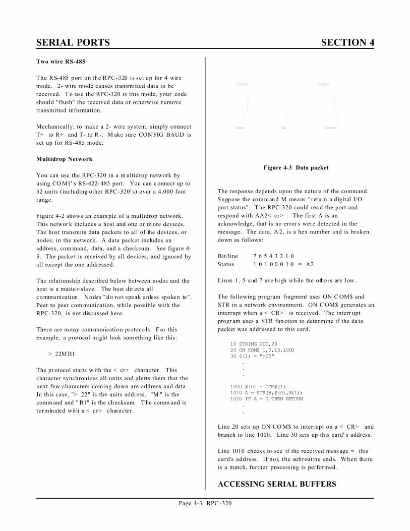
Figure 4-3 Data packet
Two wire RS-485
The RS-485 port on the RPC-320 is set up for 4 wire
mode. 2- wire mode causes transmitted data to be
received. T o use the RPC-320 is this mode, your code
should "flush" the received data or otherwise r emove
transmitted information.
Mechanically, to make a 2- wire system, simply connect
T+ to R+ and T- to R -. M ake sure CON FIG BAUD is
set up for RS-485 mode.
Multidrop Network
You can use the RPC-320 in a m ultidrop network by
using CO M1' s RS-422/ 485 port. You can c onnect up to
32 units (including other RPC -320' s) over a 4,000 foot
range.
Figure 4-2 shows an exam ple of a multidrop network.
This networ k includes a host and one or m ore devices.
The host transmits data packets to all of the devices, or
nodes, in the network. A data packet includes an
address, com mand, data, and a checksum. See figure 4-
3. The packe t is received by all devices, and ignored by
all except the one addressed.
The relationship described below between nodes and the
host is a maste r-slave. The host dir ects all
communication. Nodes "do not speak unless spoken to" .
Peer to peer com munication, while possible with the
RPC-320, is not discussed here.
Ther e are m any com municatio n protoco ls. F or this
example, a protocol might look som ething like this:
> 22M B1
The pr otocol starts w ith the < cr> charac ter. This
character synchronizes all units and alerts them that the
next few characters coming down are address and data.
In this case, "> 22" is the units address. "M " is the
comm and and " B1" is the ch ecksum . T he comm and is
terminated with a < cr> character.
The response depends upon the nature of the command.
Suppose the command M means "return a digital I/O
port status". T he RPC-320 could rea d the port and
respond with AA2< cr> . The first A is an
acknowledge, that is no error s were detected in the
message. The data, A 2, is a hex number and is broken
down as follows:
Bit/line 7 6 5 4 3 2 1 0
Status 1 0 1 0 0 0 1 0 = A2
Lines 1, 5 and 7 are high while the others are low.
The following program fragment uses ON C OM$ and
STR in a network environment. ON C OM$ generates an
interrupt when a < CR> is received. The interr upt
progr am uses a STR fun ction to deter mine if the da ta
packet was addressed to this card.
10 STRING 200,2020 ON COM$ 1,0,13,100030 $(1) = ">05"
.
.
.
1000 $(0) = COM$(1)1010 A = STR(8,$(0),$(1))1020 IF A = 0 THEN RETURN
.
.
Line 20 sets up ON CO M$ to interrupt on a < CR> and
branch to line 1000. Line 30 sets up this card' s address.
Line 1010 checks to see if the rece ived mess age = this
card's address. If not, the subroutine ends. When there
is a match, further processing is performed.
ACCESSING SERIAL BUFFERS

SERIAL PORTS SECTION 4
Page 4-4 RPC -320
You can access C OM0 and COM 1 buffers in three w ays:
1. INP UT sta tement. This re moves a ll charac ters in
the buffer up to the term inator cha racter and puts
them into a variable.
When using the INPUT statement, program
execution is susp ended until a < cr> (Enter key) is
received. W hether this is a problem depends on
your particular application.
INPUT strips bit 7. This means ASCII characters
from 0 to 127 are rec eived.
2. GET function. Char acters ar e rem oved one at a
time as an ASCII value. A 0 is returned when the
buffer is e mpty. Use the C OM function to
determine if the buffer is empty or if a 0 is an
ASCII value. Use UIn to select the serial port for
G E T.
If you don' t read the b uffer an d the buffer fills, all
subsequent characters are discarded.
3. COM$(n) retrieves all characters in the buffer,
including other control codes (except CR).
ACCESSING COM0 AND COM1
INPU T and GET functions retrieve data using the UIn
comm and. UI0 r outes inputs to C OM 0 while U I1 inputs
from the CO M1 port. PRINT outputs are set by the
UOn command. UO0 prints out COM0 while UO1
outputs COM1 using the PRIN T comm and. PR INT #1,
is an alternative way to print to COM 1.
The following show how UIn and U On work.
100 UI0 Set to COM0
110 INPUT A Get data from COM0 port
520 UI1 Switch to COM1 port
530 INPUT B Get data from COM1 port
800 REM Prin t to COM0
810 PRINT "Temperature:" ,T
900 REM Print to COM 1
910 PRINT#1, "Set pressure at:" ,CA
Power up default is set to COM 0.
DISABLING CONTROL-CProgram execution is terminated by entering a
< Cntl> < C> . To disable < Cntl> < C> so program
execution is not terminated, execute the following
statemen t:
DBY(38) = DBY(38) .OR. 1
COMMANDS
The following is a list of RPBASIC-52 commands used
for serial I/O. These commands and functions are
explained in the BASIC-52 Programm ing Manual and
RPBASIC-52 Software Supplement in this manua l.
Comm and Function
CLEAR COM$ Clears serial input buffer
COM$ Returns string from buffer
COM Returns number of characters
in buffer
CONFIG BAUD Sets serial port parameters
GET Returns a character fr om the
serial buffer
INPUT Receives string from port
LIST Outputs program listing
PRINT Outputs data in various
form ats
PRINT #, Prints to a specified port
SPC Print out n number of spaces
STR String handling commands
TAB Tabs to predetermined
positions
UI0 Reroute inputs to COM0
UI1 Route inputs to COM1
UO0 Rerou te PRIN T statem ent to
COM0
UO1 Route P RINT statement to
COM1
USING PRINT formatting statement
SERIAL PORT PIN OUT
Pin outs for J1 and J2 are shown below. Unused pins
are open.
J1 & Name Direction
J2 from card
3 Tx Out
4 RTS* In

SERIAL PORTS SECTION 4
Page 4-5 RPC -320
5 RXD In
6 CTS Out
9 Ground
10 + 5
*RTS input not in COM0.
A seria l cable is ma de by simp ly taking a 10 pin fe male
IDC connector and crim ping a 9 wir e ribbon c able to it.

RAM MEMORY SECTION 5
Page 5-1 RPC -320
Figure 5-1 RAM and W1 ju mper location
INTRODUCTION
32K, 128K, or 512K of RAM may be battery backed on
the RPC-320. RA M size can be changed at any time.
RAM is in socket U5.
RAM is backed up when a DS1216DM is installed.
Battery life depends upon RAM size, its power
consumption, ambient temperature, and amount of time
the board is operating. Gener ally, a battery life of about
3 to 5 years is e xpec ted . Op er ati ng the boar d a t 50 °C
reduces battery life by 1/2.
The DS1216DM is also a real time clock. Thus, DATE
and TIM E function s and com mands a re availa ble when it
is installed. See Chapter 7 for more inform ation.
This chapter discusses changing RAM, saving and
retrieving variables, r unning assembly language
program s, and battery condition. F igure 5-1 shows the
location of U3 and jumper W1.
Increasing RAM size does not necessarily increase the
program size RPBASIC-52 can handle. Maximum
program and variable size is 60K. Additional RAM does
increase the amount of space available for PEEK and
POKE storage.
CHANGING MEMORY
Different types of memory can be installed at any time.
RPC-320 models come with either 32K or 128K of RAM
installed. Maximum is 512K.
To change a mem ory chip, you need to rem ove the
original chip, install the new one, and set jumper W 1.
To install a new memory chip:
1. Turn off power to the RPC-320.
2. Remove the mem ory chip from U 5.
3. Orient the chip so pin 1 is towards the inside.
If installing a 32K RAM , place the chip at the
bottom of the socket (m emor y chip pin 1 goe s into
socket pin 3). The top two socket pins in each row
are empty.
If installing a 128K or 512K, install the chip into the
socket.
4. Check and change , as n ecessar y, jum per W 1 to
conform to the new mem ory.
RAM size Jumper W1
32K [1-2]
128K [1-2]
512K [2-3]
BATTERY BACKUP
An optional battery backup module may be installed.
Principal is the same as installing a RAM chip.
WARNING:An additional modification must be performed to the
DS1216DM module when a 512K RAM is installed.
Contact Rem ote Processing fo r details.
To install a module:
1. Remove the RAM IC in U5.
2. Install the DS1216DM in U5.
3. Re-install the RAM chip into the top of the module.
Checking the battery
Battery voltage is approximately 3.0 volts, measured
between pin 16 (ground) and 30 (128K RAM ), 14 and 28
(32K RA M), or 16 and 32 (512K R AM ) on the IC itself
(not the circuit side of the board). Be sure to pow er up
the RPC -320 once to a ctivate the batter y backup cir cuit
in the module.

RAM MEMORY SECTION 5
Page 5-2 RPC -320
Figure 5-2 RPBASIC-52 memory map
RESERVED MEMORY
Many control systems use process variables that are
operator entered. "variables" in this context include
numbers, strings, ar rays, recipes, or formulas as applied
to your application. They are not a part of the variables
used by Basic. Process variables are accessed by PEEK
and POK E type statements.
The upp er 512 by tes of mem ory ar e set aside for this
purpose in a 32K RAM system. In 128K and 512K
RAM systems, all of the first 64K of RAM is used for
program and variable stora ge. P rocess var iables in these
larger versions are stored starting at segment 1 and
higher.
When the combined program and data size exceed 30K,
a 128K or 512K RA M is nec essary. Additional R AM is
necessary when your pr ogram has large ar rays and / or
string storage r equireme nts.
MTOP should not be used when variables are battery
backed for power off conditions. Basic clears all of
RAM in segment 0 (except for the last 512 bytes in a
32K system) at power up. Store process variables
starting at segment 1 or higher in a 128K or 512K RAM
system or start at address 7E00H, segment 0 in a 32K
RAM system.
STORING VARIABLES IN RAM
Program s and RPBASIC-52 var iables reside in segment
0. D ata is generally stored in segment 1 and higher (a
segment is 64K of memory). See memor y map figure 5-
2. "Data Area" is segment 1 or higher.
PEEK and PO KE commands store and retrieve values
from memor y. For example:
20 POKEB1,12,A
puts the 8 bit value of A into segment 1, addr ess 12.
Use the PEEK statement to retrieve the variable:
50 B = PEEKB(1,12)
Accessing reser ved mem ory in a 32 K RAM system is
accomplished as follow s:
100 POKEB0,7E00H,C120 B = PEEKB(0,7E05H)
The highest address in a 32K RAM system is 7FFFH.
Many times it is desirable to store an array containing a
"mixed" set of variables. Suppose you needed to save an
array m ade up of the following elem ents:
Bytes Type Description
1 Byte Job counter
2 Word Analog output offset
6 Floating Corr ection factor
20 String Job name
Total number of byes required for each array is 30 (add
1 for a < CR> at the end of the string).
The Job c ounter is inc rem ented ever y time it is
completed. A nalog output offset is an output constant or
other var iable used to initialize the outputs. Job name is
used with the display to identify a job.
For this example, suppose there are 20 of these arrays
that need to be set up. A program fragment is as
follows:
100 STRING 400,20 Initialize 20 string arrays
300 NO = 12 Elem ent to fill
310 CF = 23.432 Corr ection factor
320 JC = JC + 1 Job counter
330 AC = 25 Analog offset
350 GOSUB 1000
500 NO = 5 Element to retrieve

RAM MEMORY SECTION 5
Page 5-3 RPC -320
510 GOSUB 2000 Retrieve variables
This subroutine stores variables CF, JC, and AC into an
array starting in segment 1, address 0.
1000 POK EB1, 30*NO, JC
1010 POKEW1,30*NO+ 1,AC
1020 POKEF1,30*NO+ 3,CF
1030 POKE$1, 30*NO+ 9,$(0)
1040 RETURN
Subrout ine 2000 - 2040 retr ieves data into var iables CF,
JC and AC.
2000 JC = PEEKB(1,30*NO)
2010 AC = PEEKW (1,30*N O+ 1)
2020 $(1) = PEEK$(1, 30*NO+ 9)
2030 CF = PEEKF (1,30*N O+ 3)
2040 RETURN
You can store and retrie ve strings a nd variab les in this
way. Ther e are many variations of PEEK and POKE
statements. Refer to the RPBASIC-52 Software
Supplement in this manual for additional information and
examp les. A list of comm ands appea rs at the end of this
chapter.
BLOCK DATA TRANSFER
Blocks of data are transferred to and from RA M and
flash EPR OM u sing BLOAD and BSAVE comma nds.
Block transfers are useful for loading and storing data,
look-up tables, text, etc. U p to 65,535 bytes can be
moved from RAM to EPROM or EPROM to RAM at
one time. The absolute number of bytes that are moved
is limited by the RAM and EPR OM sizes.
Transfers from EPRO M to RAM , using BLOA D, take
approximately 23.5 m s/1000 bytes. T ransfers from
RAM to EPROM , using BSAVE , are even longer at 100
ms/ 1000 bytes usin g a 512K byte EPR OM . T his time is
even longer when smaller E PROM s are used (due to the
program ming algorithm).
Serial port, tick timer, and external interrupts are
enabled dur ing these tra nsfers. Howe ver, response s to
ONT ICK or ONIT R are d elayed by the time it takes to
transfer data. W hen ONTIC K or ONIT R must be
serviced faster, transfer data in sm aller blocks.
Refer to BLOAD and BSAVE in Appendix A for more
information.
ASSEMBLY LANGUAGE INTERFACE
Assembly language program s must be placed in the
RPBASIC-52 E PROM . W hen using RPBASIC-52,
progr ams shou ld start at addr ess 6000H or higher up to
7FFFH.
RPBASIC is norm ally in a 32K byte EPROM (27C256).
A 64K byte EPROM (27C512) may be used in socket U4
provided the following modification is made: Cut the
trace between W11 pins 1 and 2 on the circuit side.
(Jumper W11 is under socket U4. P in 1 is designated by
the square pad.) Solder a jumpe r between W11 pin 2
and 3.
Docum ented assem bly language interface calls listed in
the Intel MCS BASIC -52 Users Manual will not work
with RPBASIC-52. This is because RPBASIC-52 has
been reassembled and code shifted around.
The RP-10 adapter boar d is used to run and debug
assembly and C code. This board plugs into RAM
socket U5 and RPBASIC socket U4. It does not use the
Basic at all.
COMMANDS
The following is a list of RPBASIC-52 commands used
with RAM.
Comm and Function
BLOAD Transfers data from EPROM to RAM
BSAVE Transfers data from RAM to EPROM
CALL Calls an assembly language routine
CBY Return s code m emor y data
DBY Returns or assigns internal memory
MTOP Sets top of RAM memory
PEEK B Return s a byte
PEEK F Returns a floating point number
PEEK W Returns a 16 bit value
PEEK $ Returns a string
POKE B Stores a by te
POKE F Stores a floating point number
POKE W Stores a 16 bit value
POKE $ Stores a string
XBY Returns or assigns external memory

DIGITAL AND OPTO PORTS SECTION 6
Page 6-1 RPC -320
Figure 6-1 Digital I/O
INTRODUCTION
Digital I/ O lines ar e used to inter face with op to-module
racks, switches, low current LED's, and other TTL
devices. The RPC-320 has 34 of these lines. 8 TTL I/O
lines go to a terminal strip. Additionally, there is one
high curr ent output and a n opto-isolated inp ut. R efer to
the figure below for the location of these lines.
Eight lines at P6 are intended for general purpose TTL
I/O such as switches, level sensors or to drive other
devices.
A 24 line con nector, J3, is inte nded to inter face to opto
racks or other TT L devices. 8 of these lines are high
curr ent outputs, capable of sink ing 75 to 200 m a. O pto
modules on an opto rack sense presence of AC or DC
voltages or switch them.
L8 at P2 is a "zero" ohm FE T switch. It is intended for
switching L ED b ack lighting on a n LC D display. This
line may also be used to switch high current, high
voltage power . It can sw itch up to 2 amps.
ISOA/B is used as an isolated input as well as an
interr upt.
In addition to the 24 I/O lines from J3, the display port
can be used as digital I/O. Refer to Chapter 8 for more
information.
WARNING:Apply power to the RPC -320 before applying a
voltage to the digital I/O lines to prevent current
from flowing in and damaging devices. If you
cannot apply power to the RPC-320 first, contact
technical support for suggestions appropriate to your
application. Power may be applied to ISOA/B at
any time.
Several softwar e comm ands support the digital I/O ports.
ON L INE br anches to a subroutine w hen a line changes.
ON C OUN T counts the number of high to low
transitions at a digital line. Maxim um coun ting rate is
about 95 Hz. T hese commands simplify design and
greatly speed up execution. See Appendix A for more
information.
DIGITAL I/O PORTS
All ports use an 82C55 for I/O. Lines are accessed
using LINE or LINEB commands. Lines at J3 and P6
are configured for inputs or outputs using the CONF IG
LINE comm and. See Appendix A for information.
WARNING:When using CON FIG LIN E, output lines go low
momentarily (less than 10 micro-seconds) until they
are set high again as per the data in the command
line. Some other lines are affected when C ONF IG
LINE 0 is executed. Refer to CONFIG LINE
command in Appendix A for more inform ation.
Digital Por t J3
This port is used to interface opto modules (using the
MP S series racks), drive small r elays, solenoids,
motors, or lamps, and provide general purpose TTL I/O
to other logic devices or mechanical switches. The
LIN E com mand is use d to access an d control this p ort.
The lines on J3 are divided into 3 eight bit groups from
an 82C55. Ports A and B are configured as all inputs or
outputs. Port C is progr amm ed as one gr oup of 8 inputs
or outputs or as two groups of four lines (upper and
lower C). T he four lines in upper and lower C can each
be prog ram med as a ll inputs or outp uts. R efer to T able
6-1 to determine the opto channel or J3 pin number for a
port. U se CON FIG LIN E 100 (Appendix A) to
configure por ts A, B, and C for inputs or outputs.
When a line is configured as an output, it can sink a
maximum of 2. 5 ma at 0.4V and can source over 2. 5
ma. Outputs sink 15 ma at 1. 0V. This will dr ive opto
modules. P ort B is connected to a high current sink
through U12. See "High current output" later.
Digital I/ O lines at J3 m ay be pulled up to + 5 volts or to
DIGITAL AND OPTO PORTS SECTION 6
Page 6-2 RPC -320
ground through a 10K/100K resistor packs using jumper
W7. 10K is on digital port A only.
Jumper W7 for pull up or down configuration is as
follows:
W7[1-2] Pull up
W7[2-3] Pull down
Setting W7 for pull up makes interfacing to switches and
"open collector" TTL devices easy . See "Inter facing to
Switches and other devices" below.
Digital Port P6
Connector P6 has 8 digital I/O lines for general pur pose
use. Additionally, 3 ground and a + 5V positions are
provided. + 5V power and gr ound may be brought in or
taken from this connector. L ines are numbered L 0-L7.
This por t may be u sed to interfa ce switche s, dr ive small
LED' s, and provide general purpose TTL I/O to other
logic devices. Voltage and current param eters are the
same as J3 except there is no high current output. Port
C from an 82C55 is used for this I/O.
Upon po wer u p or r eset lines L0 to L3 ar e inputs while
L4 to L7 are outputs. Lines L4 and L5 are low while L6
and L7 a re high at p ower up. All lines are connected to
a 10K pull up resistor (R21). Lines are r econfigured for
all inputs or outputs using the CONFIG LINE 0
command, found in Appendix A.
High Current Port L8
L8 will switch 2 amperes to ground through a "zero
ohm" FET switch. Maxim um off vo ltage is + 50 volts
DC. "ON" resistance is about 0.5 ohm.
Use this port to switch LED back lighting for LCD
displays on or off under softwar e control.
This line is always an output. Use the LINE 8 com mand
to turn this line off or on.
LINE 8,ON
LINE 8,1 Both commands turn on L8.
The F ET sw itch is rated fo r mu ch higher curr ent.
However, continuous current is much less without a heat
sink attached. You may dr aw more than the rated 2
amps on an intermittent basis. How m uch and for how
long depend s upon your application. A quick w ay to
check for excessive current is to touch (VERY
CARE FUL LY!) Q2 (next to P2). It can be warm to hot
to the touch. Consider the maxim um ambient
temper ature the b oard w ill operate a t. A t 70°C, warm to
the touch at room temperature m ay be too much.
Consider adding a heat sink.
The PW M com mand m ay be used with this port. Use
the circuit in Figur e 6-2 when switching induc tive loads.
Use the "GN D" ter minal next to L8 when switching
loads.
Optically Isolated Input
ISOA a nd ISOB ar e inputs to an optica l isolator. This
input is read as L8. It can also generate an interrupt
provided W8[1-2] is jumpered and ONITR is set. Refer
to Chapter 12 for input voltage and interrupt
requirements. This line can be used to "wake up" the
CPU fr om low power IDLE 2 mode.
The status is read using the LINE(8) function.
A = LINE(8)
A 1 is returned when there is no input and a 0 when
voltage is sufficiently high enough to turn on the isolator
(about 3.5 volts).
The opto isolator is not polarity sensitive. This input can
be used in conjunction with or independently of the
ONIT R statem ent.
Digital I/O Commands
The CON FIG LINE statement is used to configure lines
at J3 and P 6 for inputs a nd outputs. J3 power up default
is all inputs. P6 pow er up de fault is L0 to L 3 are inpu ts
and L4 to L7 are outputs. CONFIG LINE 0 refers to P6
while CON FIG LIN E 100 to J3.
The L INE comm and has 3 vari ations: LIN E, LIN E B,
and LINE #. Each is described below. See Appendix A
for more inform ation.
LIN E function and statem ent is used with M PS-X X opto
rack at J3. It accesses a module according to the
position number printed on the MPS board. Lines are
numbered from 100 to 123. The opto module number
used in this command is computed by adding 100 to the
board position number. LINE also accesses L0-L 8 on
P2 and P6.
The LIN E B function and statement is used to acc ess

DIGITAL AND OPTO PORTS SECTION 6
Page 6-3 RPC -320
digital I/O lines 8 bits at a time . T he addr ess for po rt A
is 0, B is 1, and C is 2. J3 I/O bank number is 3.
Address for lines L0-L7 at P6 is 2 and I/O bank number
is 5.
LINE # function and statement accesses lines according
to the pin number at J3. J3 lines are number ed from 101
to 125. The line nu mber used in this com mand is
computed by adding 100 to the connector pin number.
Line 102 is not allowed as it is the + 5V supply. See
table 6-1 to cor respond a pin numb er to a por t and opto
rack position.
P6 lines are numbered 0 to 7, and correspond to the
terminal number on the boar d. The L INE function and
comm and are used to acc ess these lines. L 8 at P2 is a
high current output and is accessed using LINE 8. T he
status of ISOA/B is returned using LINE 8 function.
LIN E, LINE B and LIN E # re turn a ' true' logic level.
A ' 1' indicates + 5 volts or high and a '0' is low or
ground. LINE B and LINE # output true logic levels.
LINE, however, outputs inverted logic. In order to turn
on an opto m odule, a line must go low. Howe ver, to
turn on a module using LINE, specify ' 1' or ON. High
curr ent output chip U 12 inverts c ontrol signa ls sent to it,
regardless of comm and.
100 LINE 118,1 :REM Turn opto 118 ON110 LINE 118,ON :REM Turns opto 118 ON120 LINE#104,0 :REM also turns 118 ON
ON LIN E is a multitasking command. W hen active, the
RPBASIC oper ating system checks the specified line
every 5 ms. If the line changed state from the previous
scan, a software interr upt is set. Upon completion of the
current BASIC command (and assuming no other
interrupts are active), pr ogram execution branches to a
specified subroutine. This command is useful for
monitoring lines, such as limit or door switches, that
may not change often or when the program structure
make it unwieldy to check lines frequently.
Another multitasking command, ON C OUN T, causes the
operating system to ch eck the specified line every 5 m s.
Up to 8 lines are monitored. If the line changed from a
high-to-low state, a counter is incremented. M aximum
counting rate is effectively 95 Hz. This command has
two variations. One causes a software interr upt when a
specified num ber of co unts is reac hed. Another simply
counts pulses at a line. The C OUN T function returns
the number of pulses since ON CO UNT was initiated.
See Appendix A for command infor mation.
ON C OUN T and O N LIN E do not ne cessarily h ave to
be input lines. They can be outputs controlled by
another part of the program.
High Current Output
Eight lines at J3 can be used as high cur rent driver s.
These outputs will switch loads to ground. Outputs are
controlled by Port B on the 82C55.
Logic outputs are inverted. That is, when a 1 is written
to the high current port, the output is switched on and
goes low.
The output driver chip, U 12, can be replaced w ith a DIP
shunt jumper so it is like the other lines at J3. To do
this, r emove U12. Install a DIP shunt so pin 1 goe s to
pin 18. Pins 9 & 10 ar e open.
NOTE: Outputs at the high current lines are not
compatible with TTL logic levels and should not
be used to drive other logic devices.
Each of the high current outputs can sink 500 ma at 50V.
How ever, package diss ipation will be ex ceeded if all
outputs are used at the maximum rating. The following
conserv ative guidelines a ssume the number of outputs
are on simultaneously:
# of outputs Maximum current
on per output
1 500 ma
2 400 ma
3 275 ma
4 200 ma
5 160 ma
6 135 ma
7 120 ma
8 100 ma
The ther mal time constant of the p ackage is ve ry shor t,
so the number of outputs that are on at any one t ime
should include those that overlap even for a few
milliseconds.
Incandesc ent lamps h ave a " cold" c urre nt of 11 times its
operating current . Lamps requiring more than 50 ma
should not be used unless a series resistor is installed.

DIGITAL AND OPTO PORTS SECTION 6
Page 6-4 RPC -320
Figure 6-2 Inductive load protection
Protection diodes m ust be used with inductive loads.
Refer to figure 6-2
Do not pa rallel outputs f or higher drive. This could
result in damage since outputs will not share current
equally.
The outputs at U12 are open collector. An external
device must supply power.
Interfacing Digital I/O to an opto-module rack
I/O lines at J3 can interface to an MPS-8, 16, or 24
position opto m odule rac k. L ines not going to an opto
module connect to a screw terminal on the MPS-XX
series boards. This feature allows you to connect
switches or other TTL type devices to the digital I/O
lines. The MPS-XX series boards accept G4 series
modules.
A CM A-26-24 connects J3 on the RPC-320 to the MP S-
XX bo ard. Cable len gth should be less than 2 feet.
Excessive cable lengths cause a voltage drop and
consequently unreliable operation. Make sure + 5 V and
ground is connected to the M PS-XX racks.
Before a line is set, the 82C55 chip must be initialized.
This is done using the CONFIG LINE statement. Group
inputs and outpu ts together. Refer to Table 6-1 for opto
module position, port number , and connector pin out. If
opto channels 16-23 are used, U12 should be replaced by
a DIP shunt jumper.
The LINE and LINE # com mands are used to control
and access opto modules and lines. These commands are
both functions and statements, depending upon how they
are used.
100 LINE 100, 0 Statement
110 LINE #103, 0 Statement
120 A = LINE(100) Function
130 A = LINE#(103) Function
Program line 100 turns external opto module rack
position 0 off. Program line 110 sets J3, pin 3, to a
logical 0 level. Program line 120 returns the status of
externa l opto modu le rack po sition 0. If the modu le is
"off", a 1 is returned (assuming it is an output module).
Program line 130 returns the status of J3, pin 3 as a 0 or
1.
Example: To turn on opto module in slot position 8, the
following command is executed:
LINE 108, 1
A ' 1' turns on a module while a 0 turns it off. (In actual
fact, a 0 is written at the port. )
See Digital I/ O program ming exam ple later in this
chapter.
Interfacing to switches and other devices
Switches and other digital I/O devices may be connected
directly to P6 or J3. The STB-26 terminal board
provides a convenient way of interfacing switches or
other digital I/ O device s. L ines at J3 are connected to
the STB-26 with a CMA-26 cable. Digital devices are
then connected to the screw terminals on the STB-26.
The M PS-X X serie s opto rac ks also pro vide a way to
access digital I/O lines.
Switches may be connected directly to a line. When
jumper W7 configures the resistors as pull ups, a switch
closure to ground at a line is read as a 0 using the LINE
# function at J1. 10K resistors are always pulled up at
lines L0 to L7.
When W 7 configures the input re sistors as pull downs,
one end of the switch m ust be tied to + 5 volts. If this is
not possible or convenient, a 1K resistor can be tied
between an input and + 5 volts to force it high when a
switch is open.
Digital I/ O prog ramm ing exam ple
The follow ing exam ple read s a switch at po rt A, bit 3
(J3-25) (program line 200), r eads L1 at P6 (program line
210) and turns on opto module at channel 5 (program
line 220). A LE D is controlled through the high current
port at J3-10 (port B, bit 0) (program lines 230 and 240).
For testing, a 100 ohm resistor from J3-10 to + 5 volts
can be substituted.

DIGITAL AND OPTO PORTS SECTION 6
Page 6-5 RPC -320
100 CON FIG LIN E 100,13, 1,1, 1
200 D = LINE #(125)
210 F = LINE (1)
220 LINE 105, 1
230 LINE #110,1 :REM Turn on LED
240 LINE #110,0 :REM Turn off LED
Line 100 configured the 82C55 so ports A and C are
inputs while B is the o utput.
Note that the LINE statement is us ed to contr ol both opto
modules and individual lines.
Lines can also be re ad or co ntrolled in the imme diate
mode.
PRINT LINE#(125)
returns the status at J3-25. Notice that even when a line
is configured as an output, its status can be read back.
Execute the following to control L7.
LINE 7,OFF
sets L7 low. E xecuting
LINE 7,ON
sets the line high.
LINEB is used to read and write a byte at a time.
LINEB 3,1,128
sets port B, bit 7 high and bits 0-6 are low.
Pulse Width Modulation (PWM)
Any line accessible by the L INE com mand m ay be pulse
width modulated. PW M comm and parameters determ ine
high and low time (to 5 ms resolution) and, optionally,
number of pulses.
Use PW M to control the brightness of a display (via line
8), control the speed of a motor, or output a number of
pulses to a stepper controller. Brightness control using
LED ' s is best achieved when htime or ltime are less than
5 (25 ms). O ne of the parameters should be 1.
Noticeable flicker occurs when htime and ltime sum to
more than 6 (30 ms).
See the PWM comm and in the Software Supplement for
more inform ation. Use Table 6-1 to use an output
directly from J3.

DIGITAL AND OPTO PORTS SECTION 6
Page 6-6 RPC -320
Figure 6-3 Digital I/O connector pin out (viewed from top)
Table 6-1 Conne ctor pin ou t - J3
Pin # 82C55 Description Opto
Channel
19 Port A, line 0 8
21 Port A, line 1 9
23 Port A, line 2 10
25 Port A, line 3 11
24 Port A, line 4 12
22 Port A, line 5 13
20 Port A, line 6 14
18 Port A, line 7 15
10 Port B, line 0 High current 16
8 Port B, line 1 High current 17
4 Port B, line 2 High current 18
6 Port B, line 3 High current 19
1 Port B, line 4 High current 20
3 Port B, line 5 High current 21
5 Port B, line 6 High current 22
7 Port B, line 7 High current 23
13 Port C, line 0 Lower C 0
16 Port C, line 1 Lower C 1
15 Port C, line 2 Lower C 2
17 Port C, line 3 Lower C 3
14 Port C, line 4 Upper C 4
11 Port C, line 5 Upper C 5
12 Port C, line 6 Upper C 6
9 Port C, line 7 Upper C 7
26 Ground
2 + 5V
DIGITAL AND OPTO PORTS SECTION 6
Page 6-7 RPC -320
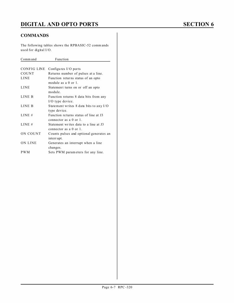
COMMANDS
The following tables shows the RPBASIC-52 comm ands
used for digital I/O.
Comm and Function
CONFIG LINE Configu res I/ O por ts
COUNT Returns number of pulses at a line.
LINE Function retur ns status of an opto
module as a 0 or 1.
LINE Statemen t turns on or off an opto
module.
LINE B Function returns 8 data bits from any
I/O type device.
LINE B Statement writes 8 data bits to any I /O
type device.
LINE # Function re turns status of line at J3
connector as a 0 or 1.
LINE # Statement wr ites data to a line at J3
connector as a 0 or 1.
ON COUNT Counts pulses and optional generates an
interr upt.
ON LINE Generates an interrupt when a line
changes.
PWM Sets PWM param eters for any line.

CALENDAR/CLOCK SECTION 7
Page 7-1 RPC-320
DESCRIPTION
An optional DS1216DM calendar/clock module m ay be
installed in U5. The DS1216D M also battery backs
RAM.
The DS1216DM from Remote Processing is a modified
version of the Dallas DS1216D. An internal reset line
has been cut. When a 512K RAM is installed, an
additional line is cut and another soldered. Contact
Remote P rocessing for de tails.
Battery life depends greatly upon the ambient
temperature. Battery life degrades up to 50% at 50°C,
using 25°C as a refer ence. RAM size and type also
affect battery life. Generally, you can expect a battery
life of 3 to 5 years.
Accuracy is about 1 minute/month and is not adjustable.
Hour s are exp ressed in 2 4-hour fo rma t.
Refer to the RPBASIC -52 Software Supplement for
more com mand information.
The cloc k module is installed by first r emoving the IC in
U5. Then, install the DS1 216DM into the socket. Install
the RAM chip into the socket. W hen installing a 32K
RAM chip, the top two pins in the DS1216DM ar e left
open.
Refer to CHAPTER 5 for information about using battery
backed RAM and jumper setting when installing a 512K
RAM.
WARNING: An additional modification to the
DS1216DM is necessary when
installing a 512K RAM. C ontact
Remote P rocessing for de tails.
SETTING DATE AND TIME
Set the date to turn on the clock module. Date and t ime
are set w hile runnin g a progr am or in the imm ediate
mode. Date and time are treated as number s and not
strings. To set the date and time:
DATE 95,11,28TIME 13,23,43
The time is set to 1:23:43 PM.
NOTE: The clock module is turned off as shipped from
the factory. DATE and TIME functions return
a HA RDW ARE erro r until DA TE is se t first.
To retr ieve date and time as part of a program:
100 PRINT "Time: ",110 FOR N=0 TO 2120 PRINT TIME(N),130 NEXT140 PRINT "Date: ",150 FOR N=0 TO 2160 PRINT DATE(N),170 NEXT180 PRINT CR,190 GOTO 100
run
Time: 13 24 12 Date: 94 11 14
When the clock mo dule is missing , de fective, or the date
has not been set, a HARD WARE er ror (code 50 at
address 101H) is returned by RPBASIC when a DATE
or TIM E function is performed. Use ONE RR to trap for
this error and report the problem.
COMMANDS
The following is a list of RPBASIC-52 commands for
the calendar/clock.
Comm and Function
DATE Sets date and tur ns on mod ule
DAT E(n) Return s date
TIME Sets time
TIME (n) Returns t ime

CALENDAR/CLOCK SECTION 7
Page 7-2 RPC-320
Figure 7-1 Calendar/Clock

DISPLAY PORT SECTION 8
Page 8-1 RPC-320
Figure 8-1 Display interface
INTRODUCTION
RPBASIC-52 and the RP C-320 interface to a variety of
displays:
VF (vacuum florescent) character
LCD (liquid crystal) character
LCD gr aphics
Character display sizes range from four lines by 20
characters to four lines by 40 characters. The graphics
display supports 160 x 128 pixels. Remote Processing
supplies these displays with appropr iate cables. A
contrast a djustment fo r LC D char acter disp lays is built
into the card.
If a display is not used, this port may be used for general
purpose digital I/O. P ort A and part of port B from an
82C55 are available. See CONNE CTOR D ISPLAY PIN
OUT below for ava ilable lines.
The cable length to a display depends upon the amount
of current it requires. A significant amount of voltage
drop occurs with a long cable. V acuum florescent and
LCD graphics cables should b e less than 2 fee t. A
charac ter LC D display c able should be less than 5 feet.
CONNECTING DISPLAYS
The display port is designed to supply all the lines
necessar y for V F and L CD displays. A custom cable
connects the RPC-320 to the display.
Displays purchased from Remote Processing include a
cable. You simply connect the 20 pin connector to the
RPC-320 L CD display port and the other end into the
display.
Addit ional power wiring is usually required for LCD
graphic and VF charac ter displays. This infor mation is
included with the display. Information content is display
dependent. Below is general information on both.
Graphic displays require additional voltages not
generated on the RPC-320. These must be supplied
externally. An external contrast adjustment may be
necessary. Y ou may be able to connect these through
screw term inal block P5.
VF c haracte r displays r equire + 5 volts and gr ound to
connector P5. This may in the form of external wires
from the main power connector on the board or power
supply.
Additional information for commands m entioned in the
following text are found in the RPBASIC-52 Software
Supplem ent in this man ual.
WRITING TO THE DISPLAY
The display type must first be set using the CON FIG
DISPLAY command. T he DISPLAY com mand is used
to print information.
PROGRAMMING EXAMPLE
The example below is for a four line by 20 character
LCD display. Even though DISPL AY statements do not
end with a comma (, ), a < cr> < lf> sequence is not
sent. Use C R to force a return to the beginning of the
line. A CR does not scroll characters on a display. You
must position the cursor to the next line.
10 CONFIG DISPLAY 120 STRING 200,3030 $(0) = "Hello world"40 DISPLAY (1,2),$(0)

DISPLAY PORT SECTION 8
Page 8-2 RPC-320
DISPLAY TYPES
RPBASIC-52' s software driver is based upon the
characteristics of the display family. Compatible VF and
LCD displays are shown below:
Manu fact. Model Type
Optrex DMC 40457 LCD 4 x 40
Optrex DMC 40202 LCD 2 x 40
IEEE 3601-90-080 VF 4 x 20
Optrex DMF 682N LCD 160W x 128D
DISPLAY CONNECTOR PIN OUT
The displa y port uses an 82C5 5 for data and contr ol.
The table below lists a pin number and its intended
function. A display may not use all lines even though
they are available.
J4 8255 Function
Pin Port/line
1 Logic + 5V
2 Digital ground
3 A/4 D4
4 Contrast voltage
5 A/6 D6
6 A/5 D5
7 B/4 Reset (from invertor)
8 B/3 Write
9 B/2 Read
10 A/7 D7
11 A/1 D1
12 A/0 D0
13 A/3 D3
14 A/2 D2
15 B/7 CS (from invertor)
16 B/6 Com mand/ data
17 B/5 Halt
18 Contrast adjust
19 Alternate power
20 Power gr ound
J4 is available for additional I/O if a display is not used.
Port A is configured as an input or output. P ort B must
be configur ed as an outpu t if a 17 key or larger keypad is
used. Use the L INE B comm and to acces s this part.
I/O bank is 4.
Pins 18, 19, and 20 are for the LCD -5003 and other
graphic displays.
COMMANDS
The following RPBASIC-52 com mands are used for the
display.
Comm and Function
CLEAR DISPLAY Clears entire display
CLEAR DISPLAY LINE Clears curr ent line
CONFIG DISPLAY Specifies display type to
use
DISPLAY Prints the string at the
row and collum specified
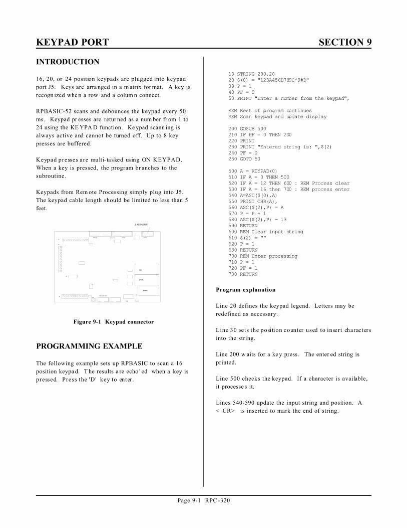
KEYPAD PORT SECTION 9
Page 9-1 RPC -320
Figure 9-1 Keypad connector
INTRODUCTION
16, 20, or 24 position keypads are plugged into keypad
port J5. Keys are arra nged in a m atrix for mat. A key is
recogn ized whe n a row and a colum n connect.
RPBASIC-52 scans and debounces the keypad every 50
ms. Keypad pr esses are retur ned as a num ber fr om 1 to
24 using the KE YPA D function . Ke ypad scann ing is
always active and cannot be turned off. Up to 8 key
presses are buffered.
Keypad presses are mult i- tasked using ON KEYPAD.
When a key is pressed, the program br anches to the
subroutine.
Keypads from Rem ote Processing simply plug into J5.
The keypad cable length should be limited to less than 5
feet.
PROGRAMMING EXAMPLE
The following example sets up RPBASIC to scan a 16
position keypa d. T he results a re echo ' ed when a key is
pressed. Press the 'D' key to enter.
10 STRING 200,2020 $(0) = "123A456B789C*0#D"30 P = 140 PF = 050 PRINT "Enter a number from the keypad",
REM Rest of program continuesREM Scan keypad and update display
200 GOSUB 500210 IF PF = 0 THEN 200220 PRINT230 PRINT "Entered string is: ",$(2)240 PF = 0250 GOTO 50
500 A = KEYPAD(0)510 IF A = 0 THEN 500 520 IF A = 12 THEN 600 : REM Process clear530 IF A = 16 then 700 : REM process enter540 A=ASC($(0),A)550 PRINT CHR(A),560 ASC($(2),P) = A570 P = P + 1580 ASC($(2),P) = 13590 RETURN600 REM Clear input string610 $(2) = ""620 P = 1630 RETURN700 REM Enter processing710 P = 1720 PF = 1730 RETURN
Program explanation
Line 20 defines the keypad legend. Letters may be
redefined as necessary.
Line 30 sets the position counter used to insert characters
into the string.
Line 200 w aits for a ke y press. The enter ed string is
printed.
Line 500 checks the keypad. If a character is available,
it processe s it.
Lines 540-590 update the input string and position. A
< CR> is inserted to mark the end of string.

KEYPAD PORT SECTION 9
Page 9-2 RPC -320
The second example uses ON KEYPAD to generate an
interrupt every time a key is pressed.
10 ON KEYPAD1000...
500 GOTO 500
1000 PRINT KEYPAD(0)1100 RETURN
Line 10 sets up the tasker for keypad interrupts to start at
line 1000. Line 500 loops on itself for demonstration
purposes.
Line 1000 prints out the key pad position pressed.
Elem ents of the pr evious pr ogram can be com bined with
this one to produce keypad strings.
KEYPAD PORT PIN OUT - J5
The keypad port uses ports B and C from an 82C55.
Lowe r por t C is configu red as an input. Upper port C
and port B bits 0 and 1 are ou tputs.
The table b elow lists J5' s pin out, 82C55 p ort and bit,
and its intended function.
Pin 82C55 Function
Port/ bit
1 C/0 Row 1
2 C/6 Column 3
3 C/5 Column 2
4 C/1 Row 2
5 C/2 Row 3
6 C/4 Column 1
7 C/7 Column 4
8 C/3 Row 4
9 B/0 Column 5
10 B/1 Column 6

ANALOG INPUT SECTION 10
Page 10-1 RPC -320
Figure 10-1 Analog I/O
DESCRIPTION
The RP C-320 has 8 single ended analog input channels.
These channels are used to measure voltages from
transducers, 4-20ma current loops, thermistors, etc.
Input voltage r ange is 0 to 5 volts or ±2.5V with 12 bit
(4096 count) resolution. Signals are single ended or
differential. Input impedance is 100K ohms to ground.
Reference IC U 14 has a voltage output that corresponds
to the IC tem peratur e. T his output ma y be used to
measure ambient temperature.
Two am plifiers are available to signal condition inputs.
By installing appr opriate r esistors and capacitor s, inp uts
are buffered, amplified, and filtered.
This chapter begins with basic information on connecting
and using ana log inputs. Later , de scriptions of how to
measure voltages other than 2.5 or 5 volts, temperature
measurem ent, data logging, using the amplifiers, and
calibration are presented.
CONNECTING ANALOG INPUTS
All analog inputs interface through connector P4.
Additional compone nts, such as r esistors and capacitors,
may be conne cted directly to the screw terminals.
For gr eatest accuracy, connect unused inputs to ground.
R17 is adjusted to trim accuracy to your system. See
Calibration later in this chapter for more information.
Tem peratur e output or other signa l input may g o directly
to channel 0 via header H1. See Temperature
Measurement and Amplifiers below.
Overvoltage conditions
Inputs are protected over voltage protected. M aximum
voltage on 1 channel is 25 volts. M aximum voltage for
2 to 4 channels is 12 volts. Total input current m ay not
exceed 16 ma on all channels. Each channels input
current is computed by the following formula:
Iin = (V in - 5)/4700
When V in < 5 volts, no curr ent flows into the channel.
NOTE: An over-voltage condition on one channel
usually affects readings on other channels.
Grounding
Analog ground is somewhat isolated from digital ground.
While the ground plane is connected between the two,
analog ground is a virtual "island" connected only in one
place to digital ground. To minimize noise pickup, the
sending device should be connected to analog ground
(located at the a nalog input ter minal str ip). W hen both
analog and digital grounds come from the same device,
you will have to play aro und with the g rounds to
determine which scheme provides the best performance
for your system.
INITIALIZATION
Each channel is initialized for 0-5V, single ended input
upon power up. Inputs can be reconfigured for eight
single-ended, four differential, or a mixture of single-
ended and differential inputs. Input voltage ranges are 0
to 5V or ±2.5V for any single-ended channel or
differential pair. Syntax is:
CONFIG AIN channel,mode, range
channel ranges from 0 to 7 for single-ended inputs.
Differential inputs use adjace nt channels.
mode defines single-ended or differential. 0 =
differential, 1 = single-ended.
Differential inputs operate in a special way. The
polarity of the input signal must be connected as shown
for an even or odd channel. For exam ple, when channel
is odd (1, 3, 5, or 7), channel 0 m ust be more negative
than channel 1 otherwise a 0 is returned. Should the
relative polarity change, configure the even channel for
differential input and perform an AIN on it. Use the

ANALOG INPUT SECTION 10
Page 10-2 RPC -320
following tables for differ ential inputs.
When channel = odd
Pol. - + - + - + - +
CH # 0 1 2 3 4 5 6 7
channel 1 3 5 7
When channel = even
Pol. + - + - + - + -
CH # 0 1 2 3 4 5 6 7
channel 0 2 4 6
When range = 0, the input is ±2.5 v olts and a 1 = 0 to
5 volts.
Differential Mode
When d ifferential m ode is specified , inpu ts are actu ally
pseudo-differential. What this means is that a ground
reference is needed. For example, you cannot place a
battery be tween ch annel 0 and 1 and get an ac curate
reading. T he (-) input must be referenced to ground.
An example of where pseudo-differential works is an
output from a bridge network.
A pseudo-differential input subtracts the DC component
from an input. T he IC maker recomm ends the (-) input
remain stable within 1 count with respect to ground for
best results. Connecting a 0. 1 uF capacitor from the (-)
input to grou nd wor ks well.
When operating in differential mode, r elative + and -
voltages must be connected to specific inputs. When
inputs are reversed, a conversion returns a 0. When the
relative voltage changes, perform a conversion on the
alternate c hannel. CON FIG AIN is p erfor med on b oth
channels.
Pairs of channels c an be differ ential while oth ers single
ended. Thus, if channel 0 and 1 are differ ential inputs,
channels 2-7 may be single ended.
Examples u sing CON FIG AIN
Below are sample syntaxes for CO NFIG AIN
Differential, 0 to + 5V input
CON FIG AIN 0,0, 1
CON FIG AIN 1,0, 1
Per form a conver sion as nor mal:
A = AIN(0)
The difference between channel 0 and 1 is returned.
When channel 1 is more positive than channel 0, the
result is zero. The differenc e is read on channel 1 by
performing:
A = AIN(1)
Single-ended, ±2.5V input
CONFIG AIN channel, 1 , 0
The result is 0 for -2.500V input, 2048 for 0. 000V, and
4095 for + 2.4988V.
Acquiring Analog Data
Analog data is accessed with the AIN function. The
syntax is:
A = AIN(channel)
This function assigns the analog value of a channel to the
variable ; A in th is case. The value retur ned is alway s in
the 0 to 4095 range bec ause the converter is 12 bits.
Power up or reset default configures inputs to the 0-5V
range, single ended.
To view the result of a conversion in the command
mode, type:
print ain(0)
The result at channel 0 is returned. T he returned value
will always be in the 0 to 4095 range. When using a
channel in the ±2. 5V ra nge, the value r eturned is
interpreted differently. Zero count is now -2.500V,
4095 is + 4.9988, and 2048 is 0.000V.
Use the following formulas to convert a returned number
to a voltage:
0 - 5V A = .001221 * AIN(channel)
±2.5V A = .001221 * ain(channel) - 2.5
The AIN function require s about 1.5 ms to convert the
data. Additional time is needed to store the data. The
example below takes 255 data samples and stores them

ANALOG INPUT SECTION 10
Page 10-3 RPC -320
into an array which requires 6 bytes per entry. The
second example takes only two byes per entry, can save
to extended m emor y, b ut requir es a longer time to get a
data point.
The pr ogram below take s about 1. 5 ms per data point.
10 DIM A(254)20 FOR X=0 TO 25430 A(X) = AIN(0)40 NEXT
This next program saves data above MTOP . M TOP was
previously set. However, if you have 128K or more
RAM, you can POKE into segment 1 or higher. It takes
approximately 2 mS per data point and is not affected by
the memory location saved to.
10 A = 3000020 FOR X=0 TO 99930 POKE W0,A,AIN(0)40 A=A+250 NEXT
Data is retrieved using the PEEK W command.
Noise Notes
An input channel can appear noisy (change readings at
random) if unused inputs are allowed to float. To
minim ize noise (and increase accura cy), connect all
unused inputs to ground.
A high im pedance inp ut is, by definition, sensitive to
voltage pickup. Noise is minimized by running wires
away from A C power lines. A low impedance voltage
source helps to reduce noise pick up. Shielded cable can
help reduce noise from high impedance sources. Make
sure the shield is not used for power ground. U sing the
shield for power ground defeats its purpose.
Wire pairs can also be twisted. 5-6 twists/foot provides
a reasonable amount of noise cancellation.
Noise is defined in this section as any random change
from a known input. The amount of noise you can
exp ect und er nor ma l operatin g ci rc um stance s is ±3
counts for any input range.
One way to compensate for noise is to take a number of
samples and average the results. Taking 6 or more
samples would, in theory, cancel out any effects of
noise. A problem with this is noise tends to group
together. Ta king 6 readings at one time might show no
change fr om the no rm. Another 6 reading s might be a ll
high. If possible, try to spread out readings over a
period of time (several seconds if possible).
Another way is place a capacitor (0.1 to 1 mfd) between
the input terminal and ground. This is useful when the
source resistance is high.
Noise is, by definition, random . If you wer e to plot out
the deviations from a norm, it would roughly resemble a
bell shaped curve. Exper iments on the RPC-320 have
shown that 99% of the readings are w ithin the ±3 count
reading and 60% are ±1 count. Noise readings were
made with all inputs shorted to ground.
Temperature Measurement
Refer ence IC U14 outp uts a voltage pr oportiona l to its
temperature. This information is used to determine
approximate ambient temper ature in order to turn on
fans or heater s.
Vo = 2.1(T + 273)
or
T = Vo/2. 1 - 273
or
T = Vc * .581428 - 273
Where T = Te mp er atu re in °C
Vo = Output voltage in mV
Vc = Count returned using AIN , 0 -
5V range
At 25°C the output voltage is approximately 625 mV, or
506 counts. Vo is expressed as a milli-volt number
(625) not .625.
The output from U14 must be buffered. To measure
temperature, jumper H1[1-3]. Remove resistor R13.
Jumper H1[2-4]. Tem perature is read at analog channel
0. T he sensitivity is incr eased by jum pering H 1[5-7] to
ground. T his will double the output voltage and any
voltage changes due to temperature.
100 T = AIN(0) * .581428 - 273
T retur ns the tempera ture in celsius.
Sensitivity is increased by jumpering H1[5-7] to ground.
This doubles the output voltage and any voltage changes
due to temperature.
NOTE: Tem peratur e measu rem ents are a pproxim ate
and are meant as a guide to indicate ambient
temperature.

ANALOG INPUT SECTION 10
Page 10-4 RPC -320
The outpu t from the tempe ratur e sensor v aries fr om unit
to unit. Self heating effects as well as supply voltage
will change the output.

ANALOG INPUT SECTION 10
Page 10-5 RPC -320
The outpu t voltage fro m the tem peratur e sensor is
doubled by jumpering H1[5-7]. While this does not
change the range the unit operates at, it does change
increase temperature m easurement sensitivity.
Data logging on a timer tick
Some applications require that data is read at fixed
intervals. The O NTI CK con struct is used to take data in
intervals from 0. 01 to 327 seconds. The exam ple below
takes 1 sample per second until 100 samples have been
obtained.
10 DIM A(100)20 ONTICK 1,50030 REM THE REST OF YOUR PROGRAM40 REM CONTINUES80 GOTO 30500 A(N) = AIN(3)510 N=N+1520 IF N = 100 THEN ONTICK 0,500530 RETI
MEASURING HIGHER VOLTAGES
Voltages higher than + 5V are measur ed by inserting a
series r esistor to the inp ut.
The table below shows resistor values for some input
voltages using the 0-5V range.
Maximum
Input Voltage Resistor
6 20K
12.5 150K
24 380K
Use the following formula to determine the series
resistance necessar y for a m aximum voltage input:
Rs = Vi * 20000 - 100000 0 - 5V range
Rs = Vi * 40000 - 100000 0 - 2.5V r ange
Rs is the re sistor value in ohms in ser ies with the inpu t.
Vi is the maximum input voltage. W hen Rs is negative
or zero, a series resistor is not necessary.
A high Rs v alue can ca use noisy r eadings. This is
because the resistor acts as an antenna. To reduce noise,
place a 0.1 mfd to 1 mfd capacitor betw een the input
terminal and ground.
NOTE: When an input voltage exceeds the input range,
other channel values are affected.

ANALOG INPUT SECTION 10
Page 10-6 RPC -320
Figure 10-2 Amplifier circuit
CONVERTING ANALOGMEASUREMENTSInputs are converted to "real numbe rs" by perfor ming
scaling calculations in the program. The AIN function
returns values from 0 to 4095. To change these numbers
into something more meaningful, use the following
formula:
var = K * AIN(n)
n is the analog channel to read. K is the scaling
constant. K is obtained by dividing the highest number
in the range of units by the maximum AIN count (4095).
Example 1: To measure the resul ts of an A/D
conversion in volts and the voltage range is 0 to 5V,
divided 5 by 4095 to obtain K.
K = 5/4095
K = .001221
Your program could look something like:
1000 C = .001221 * AIN(N)
Example 2: Y ou want to measure a 0 to 200 PSI
pressure transducer w ith a 0 to + 5V output. Divide 200
by 4095 to obtain the constant K.
K = 200 / 4095
K = .0488
The code can then look like:
1000 B = .0488 * AIN(0)
Measuring 4-20 mA current loops
Curr ent loops is a convenient way to transmit a value
and still assure the integrity of the signal. If the line
should break, a 0 volt (or nearly so) is returned.
A 4-20 ma curr ent loop is converted to 1 - 5V by placing
a 250 ohm resistor across the input of the chan nel to
ground.
Cur rent loop r eadings ar e conver ted to engineer ing units
by performing scaling as described earlier. Since the
measur ement r ange is 1 to 5V , the count ran ge is
reduced by 20% to 3276.
If pressure were measured:
K = 200/3276
K = .06105
There is one addition factor. Since the lowest value read
is 1 V, this offset is subtracted from all readings. A 1 V
offset is 1/5 of 4095 counts, or 819. The program line
then becomes:
200 A=.06105*(AIN(N)-819)
Note that if the current loop line breaks, a negative value
is returned.
AMPLIFIERS
Two operational amplifiers are available to signal
condition inputs. Each amplifier is configured as shown
below.
Amplifiers are accessed through header connector H1.
Pin out is as follows:
H1 pin Function
1 Temper ature output from U14
2 To channel 0 analog input
3 Non-inverting input, amplifier A
4 Output from amplifier A
5 Inverting input, amplifier A
6 Approximately + 7V supply (5 ma
maximum)
7 Ground
8 Ground
9 Non-inverting input, amplifier B
10 Approximately -7V supply (5 ma
maximum)
11 Inverting input, amplifier A
12 Output from amplifier A

ANALOG INPUT SECTION 10
Page 10-7 RPC -320
Voltage outputs from pins 6 and 10 are generated by the
RS-232 chip U8. Both of these voltages go through a
100 ohm resistor to H1-10 and H1-6. Pin 10 goes to 0
volts when operating the board in IDLE m odes 1 or 2.
Pin 6 goes to about + 5 volts. These voltages may be
used to supply power to very low pow er amplifier s.
CALIBRATION
The A /D comes fa ctory ca librated for a 0 to 5V inpu t.
This range is chan ged by adjusting R17. You can adjust
the range to 5.12V. This is useful when the input is 0 -
5V and you want to know when the input is over-range.
To calibrate or adjust the voltage reference:
1. Connect the voltmeter ground to a GN D point
on the Analog IN terminal strip. Make sure
there are no other connections to the analog
ground.
2. Connect the voltmeter ' + ' lead to U14, pin 6.
3. Adjust R5 for 5.00 VDC or other voltage as
desired. D o not exceed 5.2 or go below 4. 8
volts.
COMMANDS
The following RPBASIC-52 com mands are used for
analog I/ O. Mor e inform ation is found in the appendix
of this manu al.
Comm and Function
AIN(n) Returns analog value.
CON FIG AIN (n) Configures analog input
channels

WATCHDOG TIMER SECTION 11
Page 11-1 RPC-320
DESCRIPTION
The watchdog timer is used to reset the RPC -320 if the
program or CPU "crashes" . The time r is built into the
80C320 CP U. Timed access requirem ents built into the
CPU make it high ly unlikely an er rant pr ocessor would
cancel a watchdog timer.
The watchdog should not be used in loops which do not
end quickly or ar e of indetermina te duration unless a
WDOG command is included. An example of an
indeterminate loop is one that waits for a port condition
to change.
The timer is set by executing a WDOG n command. n is
0, 1, or 2. 0 turns off the timer. 1 sets the watch dog
time to 380 ms while 2 sets it to 2.8 seconds. Executing
WDO G by itself resets the timer. WD OG must be
executed pe riodically to p revent a reset.
When the watchdog times out, a softwar e reset is
perfor med. The effe ct is lines at J3 do not ch ange as in
a power-up or har dware reset. Lines at P6, display, and
keypad port ar e reset to power -up conditions.
EXTERNAL RESET
The card is reset externally by mom entarily shorting
W10[1- 2]. R eset is also achiev ed by shor ting W10-2 to
ground. Maintain this short for at least 10 ms. The card
will then reset for abo ut 350 ms.
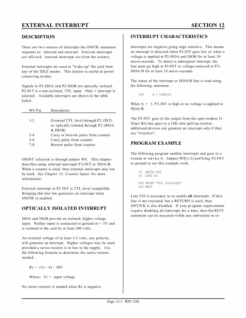
EXTERNAL INTERRUPT SECTION 12
Page 12-1 RPC-320
DESCRIPTION
There are tw o sources of interrupts the ONITR statement
respond s to: Inter nal and exter nal. Exter nal interr upts
are off-card. Internal interrupts are from the counter.
External interrupts are used to "w ake-up" the card from
any of the IDLE modes. This feature is useful in power
conserving m odes.
Signals to P2-ISOA and P2-ISOB are optically isolated.
P2-IN T is a non-iso lated, TTL input. Only 1 inter rupt is
selected. Available inte rrup ts are show n in the table
below.
W8 P in Description
1-2 External TTL level through P2 (INT)
or optically isolated through P2 (ISOA
& ISO B)
3-4 Carry or borr ow pulse from counter
5-6 Carry pulse from counter
7-8 Borrow pulse from counter
ONINT selection is through jumper W8. This chapter
descr ibes using exter nal inter rupts P 2-IN T or ISOA /B.
When a counter is used, then external interr upts may not
be used. See Chapter 14 , C ounter Inputs for more
information.
External interrupt at P2-INT is TTL level compatible.
Bringing this line low generates an interrupt when
ONITR is enabled.
OPTICALLY ISOLATED INTERRUPT
ISOA and ISOB provide an isolated, higher voltage
input. Neither input is connected to ground or + 5V and
is isolated to the card by at least 500 volts.
An external voltage of at least 3.5 volts, any polarity,
will generate an interrupt. Higher voltages may be used
provided a ser ies resistor is in line to the supply. Use
the following formula to determine the series resistor
needed.
Rs = (Vi - 6) / .005
Where: Vi = input voltage
No series resistor is needed when Rs is negative.
INTERRUPT CHARACTERISTICS
Interrupts are negative going edge sensitive. This means
an interrupt is detected when P2-INT goes low or when a
voltage is applied to P2-ISOA and ISOB for at least 10
micro-seconds. To detect a subsequent interrupt, the
line must go high at P2-INT or voltage removed at P 2-
ISOA/ B for at least 10 micro -seconds.
The status of the interrupt or ISOA/B line is read using
the following statement:
100 A = LINE(8)
When A = 1, P 2-INT is high or no v oltage is applied to
ISOA /B.
The P2-INT goes to the output from the opto-isolator I1.
Since this l ine goes to a 10K ohm pull-up resistor,
additional devices can generate an interrupt only if they
are "wired-or" .
PROGRAM EXAMPLE
The following program enables interrupts and goes to a
routine to service it . Jumper W8[1-2] and bring P2-INT
to ground to see this example work.
10 ONITR 50030 GOTO 30
500 PRINT "Got Interrupt"510 RETI
Line 510 is necessary to re-enable all interru pts. If th is
line is not executed, but a RETURN is used, then
ONT ICK is also d isabled. If your pr ogram requir ements
require disabling all interrupts for a time, then the RETI
statement can be executed within any subroutine to re-
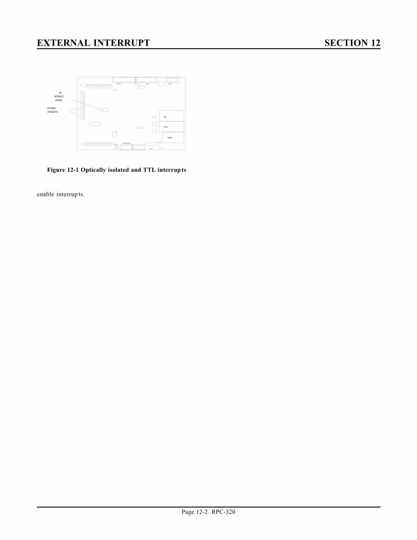
EXTERNAL INTERRUPT SECTION 12
Page 12-2 RPC-320
Figure 12-1 Optically isolated and TTL interrup ts
enable interrup ts.

MULTI-MODE COUNTER SECTION 13
Page 13-1 RPC-320
DESCRIPTION
The 24 bit multimode counter is capable of up/down,
binary, divide-by-n, and quadrature inputs. C ount
frequency is DC to 20 M hz. The R PC-320 uses an LSI
Com puter Syste ms LS 7166. Its data sheet is foun d in
Appendix C.
The COU NT function and statement are used to read
from and wr ite to the counter . L INE B is used to
program the chip for various op erating mode s.
An interrupt, using ONITR, may be detected on a carry,
borr ow, or either event. The eve nt is jumper selectable
through W8. When the counter is used, external
interrupts (see Chapter 12) may not be used.
W8 P in Description
1-2 External TTL level through P2-6 or
optically isolated through P3
3-4 Carry or borrow pulse from counter
5-6 Carry pulse from counter
7-8 Borrow pulse from counter
Signals connect to the counter via P2. Use the following
table to determine signal input to the LS7166.
P2 Function
Name
A IN Count inp ut A
B IN Count inp ut B
GND Ground
LOAD Load counter/ latch (LCTR/LLTC)
GATE Gate/reset counter (ABGT/RCTR)
Input lines (A IN), (B IN), LOAD, and GATE are
pulled to + 5V through a 10K resistor.
PROGRAMMING
The LS7166 is capable of several operating modes, all of
which are not discussed here. See Appendix C for this
chips operating modes. W hat are shown are exam ples of
how to program this chip.
NOTE: Be sure to initialize the counter chip before
using COU NT com mands. Failure to do so
returns m eaningless results.
The COU NT function returns the current counter value.
Specifically, RPBASIC w rites a 2 to the MCR (M aster
Control Register), reads the 3 counter bytes from the OL
(Output latch), and converts it to the proper internal
BASIC form at.
100 A = COUNT(0)
COUNT statement writes a 24 bit number to the PR
(Preset r egister) only. Its syntax is:
200 COU NT 0, D
To transfer this number to the counter, execute the
following in the program:
LINEB 6,1,8
The counter number is always 0 on the RPC -320.
LINEB is used to access specific registers within the
chip. Accessing control and status registers is shown
below. C ounter bank is 6.
100 A = LINEB(6,1) : REM Read OSR200 LINEB6,1,X
Line 200 writes to OCCR, ICR, QR, MCR, and ICR
register s. W hich registe r selected is determ ined by bits
6 and 7 in the byte written to the chip.
Program examples
This code resets the counter and enables the inputs. The
count is printed once a second. To see the count change,
momentarily bring " A IN" or "B IN" on P2 to ground.
When " B IN" is gr ounded, the count decrem ents.
10 LINEB6,1,3220 LINEB6,1,64+830 ONTICK 1,50040 GOTO 40500 PRINT COUNT(0)510 RETI
Line 20 can be shortened somewhat. 64 selects the ICR
(Input contr ol register ) and 8 enab les inputs. 72 could
have been used.

MULTI-MODE COUNTER SECTION 13
Page 13-2 RPC-320
The following program example returns a frequency.
Input s ignal is at "A IN".
100 LINEB 6,1,32110 LINEB 6,1,72 : REM enable inputs120 ONTICK 1,500130 IDLE140 GOTO 130500 A=COUNT(0) : REM get count510 C=A-B : REM figure change from last time520 PRINT "Frequency = ",A530 B=A530 RETI
The fir st frequen cy read will always be a bit off. This is
because of the time required to initialize ONTICK.
Subsequent readings are more accurate.
Accuracy is increased by stretching readings to every 10
seconds. This is neces sary w hen higher accura cy is
needed.
Other factors affecting accurate readings in this program
include serial communications and ONITR statement. If
ONITR is in process, ONTICK is delayed until ONITR
is finished.
The problem w ith this routine is periodically, a large
negative number is returned. This is because the
multimode counter has rolled over. This is corrected by
periodica lly reseting the CN TR or transfer ring P R to
CN TR. Refer to the data sheet, Appendix A for counter
operating mo des.
This program sets up the LS7166 to cause an interrupt
when a pr eset numb er of cou nts is reach ed. W8[7-8] is
jumpered to interrupt on a borrow.
10 LINEB 6,1,13220 COUNT 0,1000 : REM write to CNTR30 LINEB 6,1,8 : REM transfer PR to CNTR40 LINEB 6,1,72 : REM enable A/B counters50 ONITR 500100 PRINT COUNT(0) : REM print progress110 GOTO 100
500 PRINT "In Interrupt"510 RETI
Line 10 sets OCCR to divide by N. Line 50 enables
interrupts. Line 100 prints the counter. When pulses
are applied to the A input, the count will go down. When
1000 pulses are detected at A input, the message in line
500 is printed.
COMMANDS
The table below lists commands used with the counter.
Comm and Function
COU NT(0) Returns value in counter
C O UN T 0, n Writes value to counter

POWER MANAGEMENT SECTION 14
Page 14-1 RPC -320
DESCRIPTIONThere are thr ee power mana gement modes. Each mode
affects the way RPBASIC operates. T he IDLE
command is used to control how the card operates
Default mode is full power. All commands, timers, and
interrupts function. IDLE command is not used.
There are a number of ways to exit the IDLE mode in
conjunction with ONITR. Refer to Chapter 12, External
Interrupt and Chapter 13, Multi-mode Counter for ways
to generate interr upts. IDLE 2 is restricted on the type
of interrupt. T he signal at P2-INT must return to a high
state befor e the next IDLE 2 command is executed. (P2-
INT is also controlled by the multi-mode counter and
optically isolated interrupt, described in Cha pter 12 and
13.) If it does not go high, IDLE 2 mode w ill exit in
approximately 3 ms. This is due to a characteristic of
the A6 mask revision in the Dallas 80C320 CPU. A
general rule is to keep the negative pulse at P2-INT
greater than 50 ns but less than 3 ms.
IDLE or IDLE 0 waits until an ONTICK or ONITR
interr upt occur s. Se rial I/ O oper ates norm ally. U se this
comm and whe n you wan t your pr ogram to "hang out"
until something happens. The RPC-320 operates under
full power.
IDLE 1 reduce s power by 30% . H ere the C PU " shuts
down" but the internal timers are still operating.
ONT ICK and ON ITR will cause the card to come out of
power down m ode. Howe ver, the RS-232 se rial por ts
are disabled. C haracters in the transmitter buffer are not
sent out and incoming characters are ignored.
IDLE 2 is the lowest power mode. T he CPU, internal
timers , ser ial ports, and oscillator are tur ned off. Only
interrupts responding to ONITR wake up the processor.
Cur rent cons umption is less than 5 ma with no signals
going into or coming from the RPC -320.
IDLE 2 also has a number of operating restr ictions.
This mode shuts dow n the RS-232 rece iver/dr iver IC, so
no character s can come in or go out. T his IC also
supplies current for the amplifiers and analog to digital
converter. Do not apply negative voltages to the analog
input in this mode. The tick timer is shut off. However,
the real tim e clock m odule, if installed, continues to
operate.
NOTE: The RS-232 receiver is shut down in IDLE
modes 1 and 2. A ny characters sent to the
RPC-320 dur ing this time are ignored or
grossly distorted.
NOTE: Delay printing out the R S-232 ports for at least
20 ms (20 instructions) after exiting IDLE 1 or
IDLE 2. These chips generate RS-232 voltages
and require a "pow er up" time. Failure to do
so could result in garbled ch aracters.
NOTE: The < Ctl> -C break char acter is not
recognized in any of the IDLE modes.
Norm ally this is not a problem except during
progr am deve lopment. If the prog ram is
executing an IDLE statement and it won' t
respond to any interrupts, pressing the reset
button is the only w ay to exit.
Exit IDLE 2 by applying a low going pulse at the INT
input at P2. The pulse width should be 50 ns minimum.
The other IDLE modes re quire a pulse width of at least
1 micro-second. Optical interrupt ISOA/B may also be
used to exit any of the IDLE modes. The pulse w idth
needs to be at least 10 micr o-seconds.
FURTHER POWER REDUCTION
Some applications require the least amount of power
possible. You m ay rem ove cer tain IC' s from the card to
do this. The table below lists the IC 'U' number,
approximate curr ent consumption (in shutdown and run
mode), and function.
Un Curr ent Function
Run Shutdown
U9 10 mA 400 uA RS-485 interface
U14 100 uA 1.2 ma Reference for U 15,
temperature reference.
U15 5 ma 10 uA Analog to digital
converter
U11 10 mA 1 ua Digital I/O at J3
U17 10 mA 1 ua Display output, keypad
scanner.
U8 30 mA 10 uA RS-232 driver/receiver,
power supply for analog
to digital converter,
amplifiers

POWER MANAGEMENT SECTION 14
Page 14-2 RPC -320
Curr ents are maximum and minimum as specified by the
manufacturer. Min-max curr ent ranges "guaranteed" by
the device manufacturer have a tremendous range, often
by a factor of 10 or m ore. Cur rent abov e is “ty pical” .
Some current consumption is difficult to determine.
Digital outputs, for example, will draw virtually no
current under no load conditions, but can supply 15 ma
to each outpu t if requir ed. Ther efore, inputs and outpu ts
connected to the card will affect its current consumption.
Some chips, such as U 9, will not draw m uch current
unless ther e is activity on the R S-485 por t.
Board current consumption may be affected by the
setting of jump er W 7. T his jumper determ ines if inputs
at J3 are pulled up or down. When set to pull up inputs,
each line forced low increases current consumption by
50 uA. If all inputs are tied to + 5V or ground,
rem oving jump er W 7 may dr aw less cur rent.
The application program IC in U6 may be changed to a
29C040. This 512K byte memory draws 200 uA less
current than a 32K byte one.
Any contr ol line from P2 to gr ound dra ws 500 uA due to
the 10K pull-ups. Lines at P6 are pulled to + 5V
through a 10K resistor. Each low line draws 500 uA.
The contrast adjustment (R18) can be removed or
adjusted for minim um cur rent.
Program Examp le
This examp le makes the RP C-320 go into its lowest
power mode.
10 ONITR 500 . . other code .100 IDLE 2200 GOTO 100500 PRINT "In interrupt"510 RETI
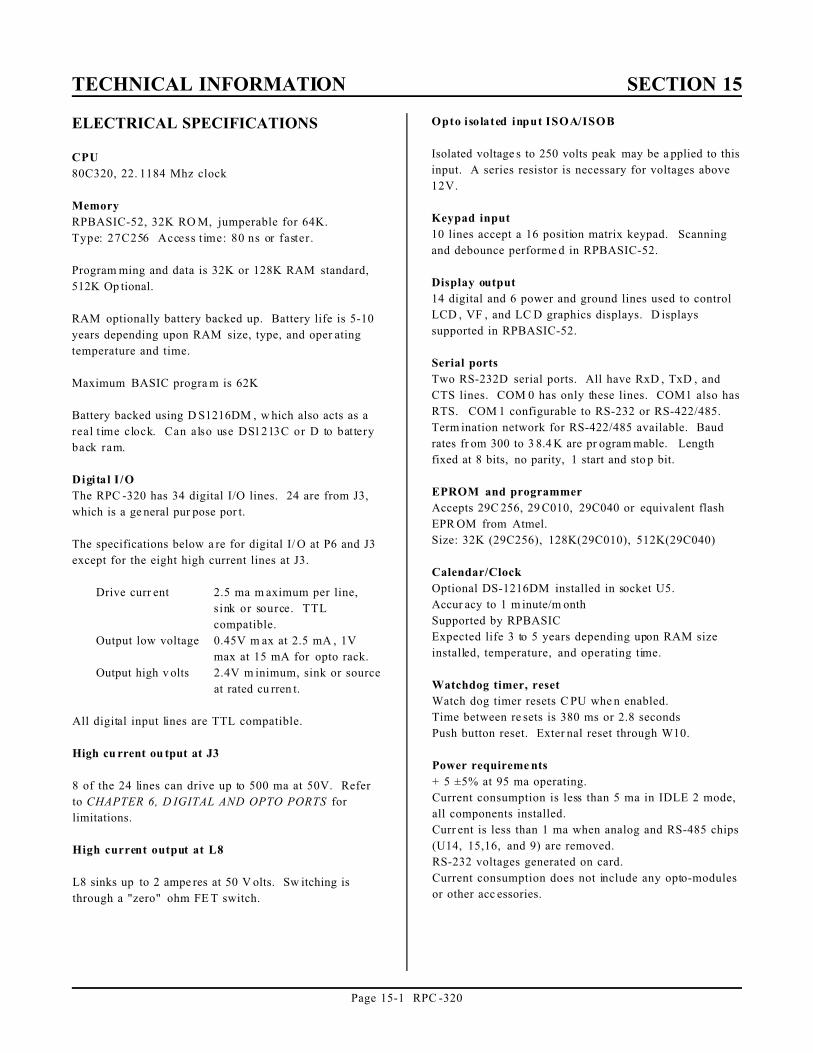
TECHNICAL INFORMATION SECTION 15
Page 15-1 RPC -320
ELECTRICAL SPECIFICATIONS
CPU
80C320, 22. 1184 Mhz clock
Memory
RPBASIC-52, 32K RO M, jumperable for 64K.
Type: 27C256 Access time: 80 ns or faster.
Program ming and data is 32K or 128K RAM standard,
512K Op tional.
RAM optionally battery backed up. Battery life is 5-10
years depending upon RAM size, type, and oper ating
temperature and time.
Maximum BASIC progra m is 62K
Battery backed using D S1216DM , w hich also acts as a
real t ime clock. Can also use DS1213C or D to battery
back ram.
Digital I /O
The RPC -320 has 34 digital I/O lines. 24 are from J3,
which is a ge neral pur pose por t.
The specifications below a re for digital I/ O at P6 and J3
except for the eight high current lines at J3.
Drive curr ent 2.5 ma m aximum per line,
sink or source. TTL
compatible.
Output low voltage 0.45V m ax at 2.5 mA , 1V
max at 15 mA for opto rack.
Output high v olts 2.4V m inimum, sink or source
at rated cu rren t.
All digital input lines are TTL compatible.
High cu rrent ou tput at J3
8 of the 24 lines can drive up to 500 ma at 50V. Refer
to CHAPTER 6, D IGITAL AND OPTO PORTS for
limitations.
High current output at L8
L8 sinks up to 2 ampe res at 50 V olts. Sw itching is
through a "zero" ohm FE T switch.
Opto isolated input ISOA/ISOB
Isolated voltage s to 250 volts peak may be a pplied to this
input. A series resistor is necessary for voltages above
12V.
Keypad input
10 lines accept a 16 position matrix keypad. Scanning
and debounce performe d in RPBASIC-52.
Display output
14 digital and 6 power and ground lines used to control
LCD , VF , and LC D graphics displays. D isplays
supported in RPBASIC-52.
Serial ports
Two RS-232D serial ports. All have RxD , TxD , and
CTS lines. COM 0 has only these lines. COM1 also has
RTS. COM 1 configurable to RS-232 or RS-422/485.
Term ination network for RS-422/485 available. Baud
rates fr om 300 to 3 8.4 K are pr ogram mable. Length
fixed at 8 bits, no parity, 1 start and sto p bit.
EPROM and programmer
Accepts 29C 256, 29 C010, 29C040 or equivalent flash
EPR OM from Atmel.
Size: 32K (29C256), 128K(29C010), 512K(29C040)
Calendar/Clock
Optional DS-1216DM installed in socket U5.
Accur acy to 1 m inute/m onth
Supported by RPBASIC
Expected life 3 to 5 years depending upon RAM size
installed, temperature, and operating time.
Watchdog timer, reset
Watch dog timer resets C PU whe n enabled.
Time between re sets is 380 ms or 2.8 seconds
Push button reset. Exter nal reset through W10.
Power requireme nts
+ 5 ±5% at 95 ma operating.
Current consumption is less than 5 ma in IDLE 2 mode,
all components installed.
Curr ent is less than 1 ma when analog and RS-485 chips
(U14, 15,16, and 9) are removed.
RS-232 voltages generated on card.
Current consumption does not include any opto-modules
or other acc essories.

TECHNICAL INFORMATION SECTION 15
Page 15-2 RPC -320
MEMORY AND I/O BANK MAP
Memory
Description Address
RPBASIC-52, U4 0000H - 7FFFH
RAM , U 5, 32K 00000H - 07FFFH
128K 00000H - 1FFFFH
512K 00000H - 7FFFFH
I/O Bank
RAM (U5) 0
EPRO M (U6) 1
not used 2
Digital I/O (U11)(J3) 3
Display & keypad (U17) 4
Control & L 0-L8 (U19) 5
Counter (U13) 6
not used 7
MECHANICAL SPECIFICATIONS
Size
4.6" x 7.0"
4 mounting holes are 0.250 x 0.250 inches from each
edge. Mounting holes are 0.124 inch in diameter.
Board thickness: 0.062
Board m aterial: FR-4
JUMPER DESCRIPTIONS
A * after a jumper position indicates fa ctory def ault is
jumpered.
Jumper Description
W1[1-2]* RAM size 32K, 128K
W1[2-3] RAM size 128K
W3[1-3],[2-4] 29C040 F lash
W3[3-5],[2-4] 29C010 Flash
W3[3-5],[4-6] 29C256 F lash
W2[1-3],[2-4] EPROM selected
W2[3-5],[4-6]* Flash EPROM selected
W4[1-2] COM 1 RS-485 input
W4[2-3]* COM 1 RS-232 input
W5[1-2]* RS-485 terminator
W6[1-2]* RS-485 terminator
W7[1-2]* J3 resistors pulled up
W7[2-3] J3 resistors pulled down
W8[1-2] External or isolated interrupt
W8[3-4] Counter carr y or borrow interrupt
W8[5-6] Counter carr y interrupt
W8[7-8] Counter borr ow interrupt
W9[1-2]* Do not autorun
W9[no jumper] Autorun on reset
W10[1-2] Exter nal reset inp ut.