Embed Size (px)
Citation preview
1
Role of Substrate Choice on LED Packaging
Steve Lester Toshiba America Electronic Components
2
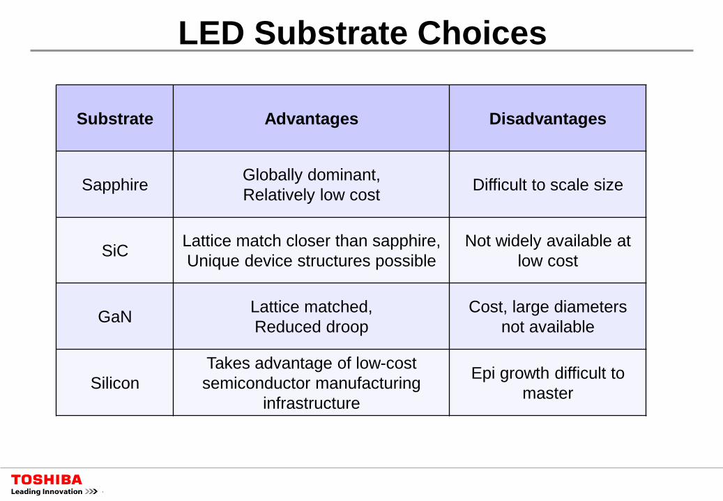
LED Substrate Choices
Substrate Advantages Disadvantages
Sapphire Globally dominant, Relatively low cost Difficult to scale size
SiC Lattice match closer than sapphire, Unique device structures possible
Not widely available at low cost
GaN Lattice matched, Reduced droop
Cost, large diameters not available
Silicon Takes advantage of low-cost semiconductor manufacturing
infrastructure
Epi growth difficult to master
3
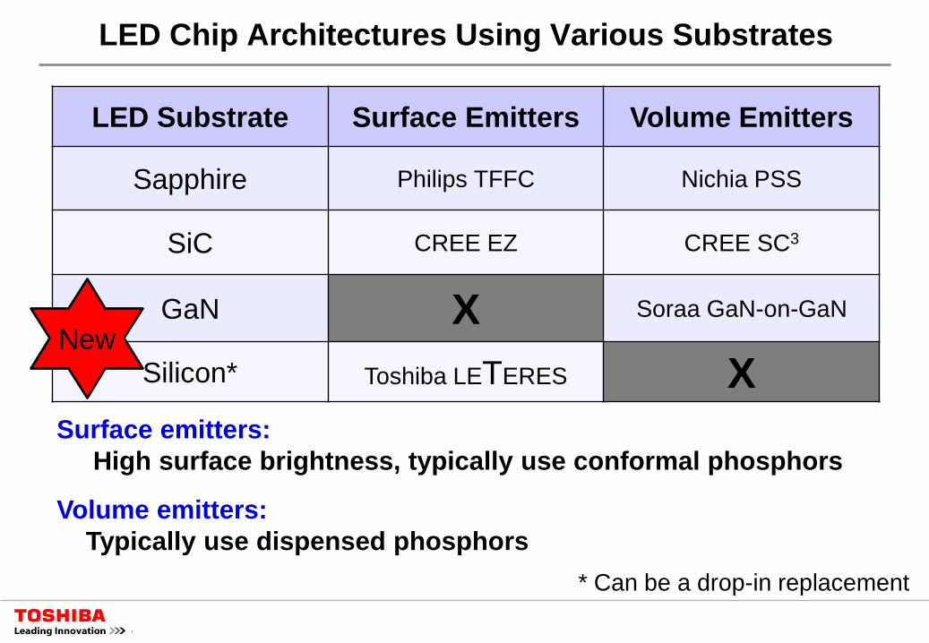
LED Substrate Surface Emitters Volume Emitters
Sapphire Philips TFFC Nichia PSS
SiC CREE EZ CREE SC3
GaN X Soraa GaN-on-GaN
Silicon* Toshiba LETERES X
LED Chip Architectures Using Various Substrates
Surface emitters: High surface brightness, typically use conformal phosphors
Volume emitters: Typically use dispensed phosphors
New
* Can be a drop-in replacement
4
Pho
spho
r/sili
cone
tem
p
Proximity of phosphor to chip
Conformal Remote
Dispensed
Goal: Operate die at high current density to reduce chip cost Problem: phosphor/silicone temperature must be controlled
Heat
The LED chips are heatsinks!
COB example:
Packaging for High Current-Density LED Operation
The phosphor solution depends on the substrate!
5
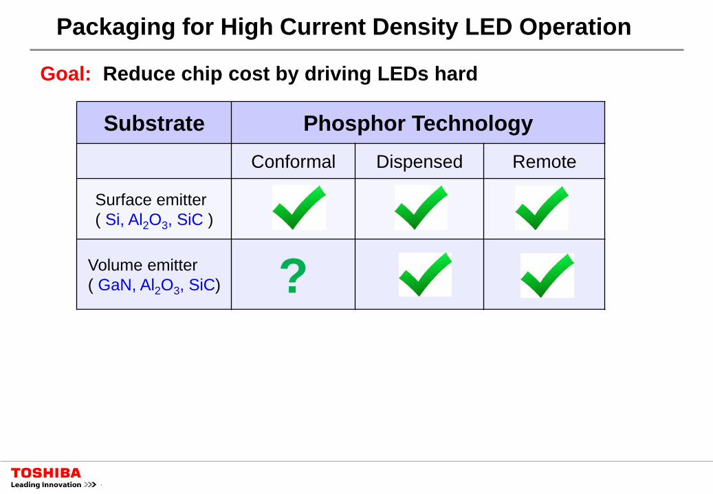
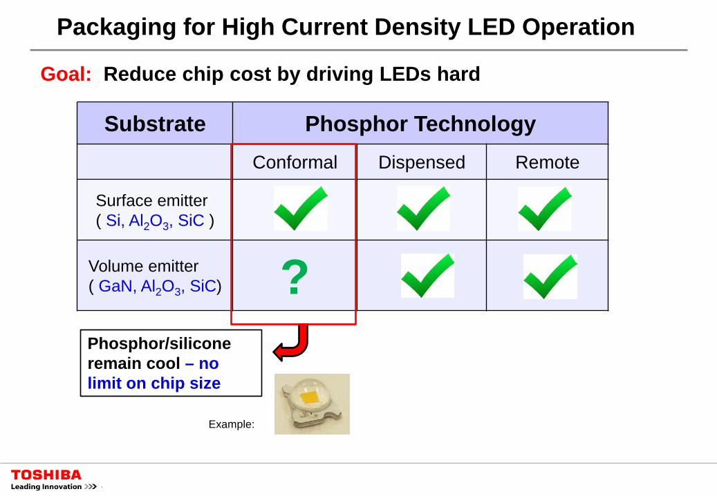
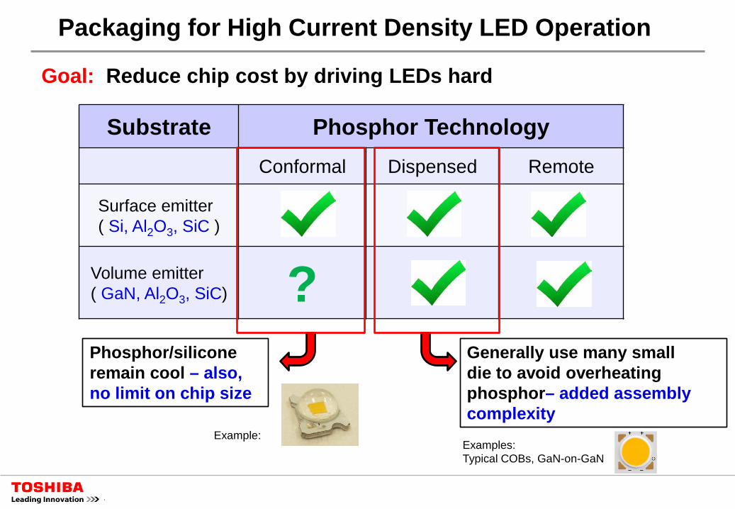
Substrate Phosphor Technology Conformal Dispensed Remote
Surface emitter ( Si, Al2O3, SiC )
Volume emitter ( GaN, Al2O3, SiC) ?
Packaging for High Current Density LED Operation
Goal: Reduce chip cost by driving LEDs hard
6
Substrate Phosphor Technology Conformal Dispensed Remote
Surface emitter ( Si, Al2O3, SiC )
Volume emitter ( GaN, Al2O3, SiC) ?
Packaging for High Current Density LED Operation
Goal: Reduce chip cost by driving LEDs hard
Example:
Phosphor/silicone remain cool – no limit on chip size
7
Substrate Phosphor Technology Conformal Dispensed Remote
Surface emitter ( Si, Al2O3, SiC )
Volume emitter ( GaN, Al2O3, SiC) ?
Packaging for High Current Density LED Operation
Goal: Reduce chip cost by driving LEDs hard
Examples: Typical COBs, GaN-on-GaN
Phosphor/silicone remain cool – also, no limit on chip size
Generally use many small die to avoid overheating phosphor– added assembly complexity
Example:
8
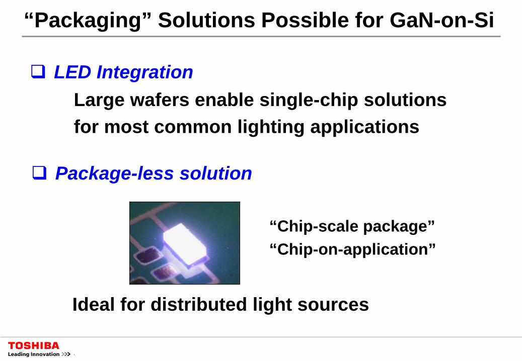
“Packaging” Solutions Possible for GaN-on-Si
LED Integration
Package-less solution
“Chip-scale package” “Chip-on-application”
Large wafers enable single-chip solutions for most common lighting applications
Ideal for distributed light sources
9
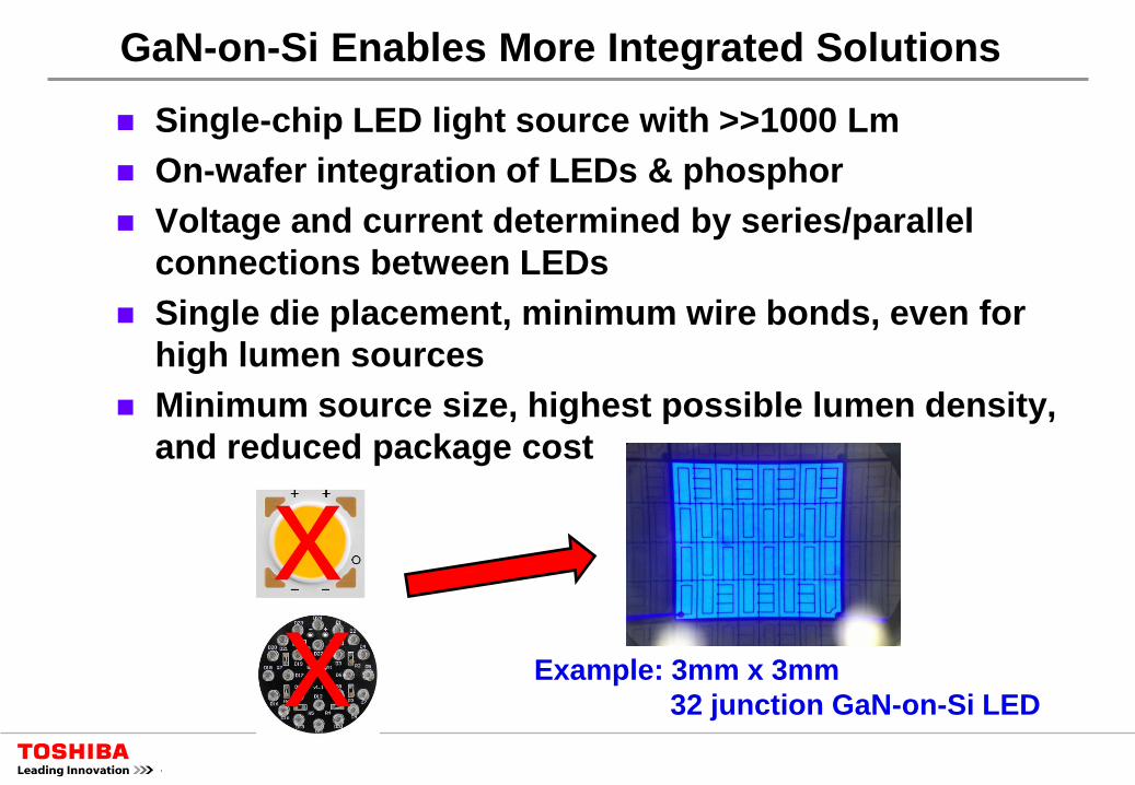
GaN-on-Si Enables More Integrated Solutions Single-chip LED light source with >>1000 Lm On-wafer integration of LEDs & phosphor Voltage and current determined by series/parallel
connections between LEDs Single die placement, minimum wire bonds, even for
high lumen sources Minimum source size, highest possible lumen density,
and reduced package cost
Example: 3mm x 3mm 32 junction GaN-on-Si LED
x x
10
0
40
80
120
160
200
0 200 400 600 800Current (mA)
Lm/W
0
500
1000
1500
2000
2500
Lum
ens
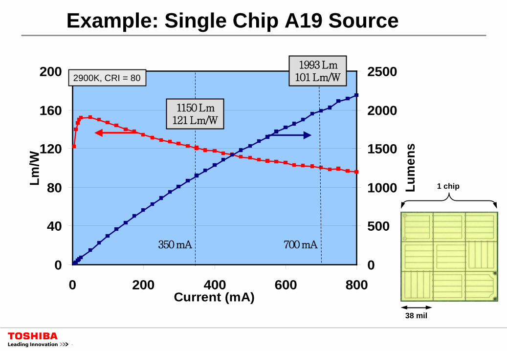
Example: Single Chip A19 Source
350 mA 700 mA
1993 Lm 101 Lm/W
1150 Lm 121 Lm/W
2900K, CRI = 80
38 mil
1 chip
11
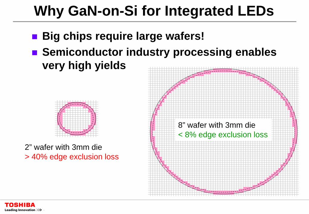
Why GaN-on-Si for Integrated LEDs
2” wafer with 3mm die > 40% edge exclusion loss
8” wafer with 3mm die < 8% edge exclusion loss
Big chips require large wafers! Semiconductor industry processing enables
very high yields
12
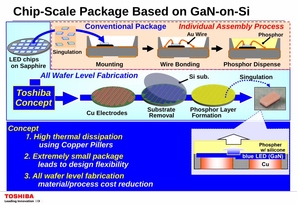
Chip-Scale Package Based on GaN-on-Si
LED chips on Sapphire
Conventional Package
3. All wafer level fabrication material/process cost reduction
1. High thermal dissipation using Copper Pillers
Concept
Phosphor Dispense Mounting Wire Bonding
Individual Assembly Process
Toshiba Concept
All Wafer Level Fabrication
Au Wire Phosphor
Singulation
Singulation
Cu Electrodes Substrate Removal
Si sub.
2. Extremely small package leads to design flexibility
Phosphor Layer Formation
13
14
Conclusion
LED substrate choice has downstream consequences for packaging
New LED substrates, Si and GaN offer unique opportunities for SSL
GaN-on-Si enables integrated, single-die sources and advanced chip-scale package architectures