Embed Size (px)
Citation preview
Ultralow-PowerLED-Enabled On-ChipOptical CommunicationDesigned in the III-Nitrideand Si–CMOS ProcessIntegrated PlatformWenjia Zhang, Bing Wang, Zhaomin Zhu,
and Kenneth Eng Kian Lee
Singapore-MIT Alliance for Research and Technology(SMART)
Li Zhang
National University of Singapore
Jurgen Michel and Li-Shiuan Peh
Singapore-MIT Alliance for Research and Technology(SMART) and Massachusetts Institute of Technology
Chua Soo-Jin
Singapore-MIT Alliance for Research and Technology(SMART) and National University of Singapore
h OVER THE PAST years, with Moore’s law supply-
ing increasing number of transistors, industry has
been boosting processor performance by increasing
the number of on-chip cores. This brings about the
challenge of designing a power-efficient on-die com-
munication backbone, e.g., network-on-
chip (NoC), for delivery of bits between
processor cores and memories. Electri-
cal copper interconnects have dominat-
ed on-chip communicat ions in
commercial processors and thus far
satisfied the communication require-
ments of current multicore processors.
However, as the number of cores grows,
the chip power budget becomes in-
creasingly constrained and electrical interconnects
will be severely limited by their fundamental tradeoff
of interconnect bandwidth and distance with power.
The power consumed by electrical interconnects
relates to the capacitance of the link, supply voltage,
and clock frequency. Since the link capacitance
increases with link length and clock frequency
(which impacts the link bandwidth), the power
consumption of an electrical link grows with dis-
tance and bandwidth. Moreover, in order to improve
the interconnect latency, long wires are routinely
Editors’ notes:This paper explores the integration of III-V-based LEDs and detectors in atraditional Si–CMOS process to power an on-die nanophotonic link. Thework also shows that the LED-enabled on-chip optical link results in moreenergy-efficient communication than using an off-chip laser source to powerthe optical link.
VSudeep Pasricha, Colorado State University andYi Xu, Macau University of Science and Technology
IEEE Design & Test2168-2356/14 B 2014 IEEE Copublished by the IEEE CEDA, IEEE CASS, IEEE SSCS, and TTTC36
Silicon Nanophotonics for Future Multicore Architectures
Color versions of one or more of the figures in this paper are available
online at http://ieeexplore.ieee.org.
Digital Object Identifier 10.1109/MDAT.2014.2346735
Date of publication: 12 August 2014; date of current version:
07 October 2014.
segmented into smaller sections, with repeaters
inserted in between, increasing total wire coupling
capacitance and thus the link power consumption.
The scaling of CMOS process technology will not
help to mitigate on-chip interconnect power con-
sumption since the long wire capacitance, instead
of the gate capacitance, dominates the load capac-
itance of on-chip interconnects, and the high wiring
density on a processor chip results in higher
parasitic interconnect capacitance, leading to ever-
increasing dynamic switching power for electrical
interconnects [1].
New interconnects are needed to ensure scal-
ability to future many-core processors. Among re-
cent disruptive technologies, optical interconnects
have the potential to break the aforementioned
bandwidth–distance–power tradeoff of electrical
interconnects. In general, a complete optical inter-
connect link is composed of a light source for
generating the information carrier, a modulator for
electrical/optical (E/O) data transformation, a pho-
todiode for detection, passive components for light
guiding, and peripheral electronic devices for driv-
ing and biasing the photonic devices. In a photonic
link, the light source is the most critical device as it
consumes a substantial fraction of total link power.
Previously proposed optical network solutions rely
predominantly on off-chip lasers as the light source.
However, laser sources consume significant power
due to their high threshold current; even when the
links are used sporadically, the power consumption
of lasers remains constant as the communication
data are typically modulated externally atop of the
continuous wavelengths, resulting in high laser
power consumption regardless of actual data trans-
mission through the optical path. Prior studies
hence conclude that laser-enabled optical inter-
connects have challenges replacing electrical inter-
connects as the on-chip communication fabric for
the highly dynamic traffic patterns of many-core
processors [1].
In this paper, we see promise in an alternative
light source for optical on-chip interconnects: the
directly modulated LED. We see two significant
strengths in LED-enabled optical interconnects.
First, the LED is a reliable light source that turns
on without threshold current. Therefore, negligible
current conducts through the device when the LED
is off, thus dissipating little power. Second, substan-
tial power can be saved as an external modulator is
no longer needed. External modulators require driv-
ers with several amplification stages that consume a
great deal of driving power, especially for high data
rate modulation with stringent driving requirements.
Furthermore, the insertion loss of a modulator, typi-
cally greater than 5 dB, worsens the optical power
budget, requiring greater output power from the
light source.
However, despite several efforts in LED device
design for communications [2], [3], there still exist
key challenges in realizing LEDs that can provide
practical, low-power, and on-chip sources.
First, LEDs typically have low modulation band-
width, typically lower than 1 Gb/s. This bandwidth
limitation is fundamentally determined by the spon-
taneous radiative recombination lifetime of injected
electrons or holes, presumably in the nanosecond
range. However, recent successes of driving the LED
to high frequencies have been achieved either by
increasing the active layer concentration of elec-
trons and holes [3], [4] or improving the bimo-
lecular recombination [2]. For instance, a directly
modulated photonic crystal nanocavity LED was
demonstrated operating with a modulation speed of
10 GHz consuming less than 1 fJ/b of energy [2].
Besides, multicore processor chip frequencies have
been plateauing at low gigahertz to alleviate the
power consumption of electronics.
Second, it is a challenge to realize a wide variety
of photonic devices, including high-speed LEDs and
detectors, and visible light transparent waveguides
within a converged process platform. Silicon (Si) is
widely considered as a future platform of choice for
building optoelectronic devices, accommodating
both Si–CMOS electronics as well as integrated pho-
tonics. For instance, IBM projected ten tera-floating-
point operations per second (TFLOPS) on a 22-nm
CMOS chip, with separate photonic, memory, and
processing planes where the CMOS-compatible Si-
based photonic plane is used for connecting various
cores and routing over 70 Tb/s of on-chip traffic and
over 70 Tb/s of off-chip traffic [5]. However, since
silicon has an indirect bandgap that offers weak
interaction between mobile charge carriers and
photons, there still remains a hurdle for active pho-
tonic devices such as light sources to be fabricated
using Si. On the other hand, III–V materials are par-
ticularly suitable for photonic devices. It will thus be
desirable to have an on-wafer integration technol-
ogy for on-chip optical interconnects where the
September/October 2014 37
electrical devices are made from CMOS processing
while the photonic devices are made of III–V
semiconductors.
In this paper, we propose a LED-enabled on-chip
optical network that leverages a novel CMOS-
compatible III-nitride and Si-integrated process,
bringing about ultralow power, small area footprint,
and competitive performance versus electrical inter-
connects on a chip scale. The rest of the paper is
organized as follows: Section III-Nitride and Si–CMOS
Optical Link Design presents an entire optical link de-
signed in a III-nitride (e.g., GaN) and Si–CMOS
integration process where design considerations of
III-nitride LED, photodetector, and visible light trans-
parent SiNx waveguide are discussed. Section Model-
ing of LED-Enabled Optoelectronic Link follows with
detailed modeling of both its electrical and optical
characteristics. Section Case Study: Optical Intercon-
nected SMART Architecture simulates the optical
single-cycle multihop asynchronous repeated travers-
al (SMART) as a case study by running actual software
applications, and evaluates our proposed network
against laser-driven NoCs and state-of-the-art electri-
cal NoCs.
III-nitride and Si–CMOS opticallink design
As GaN materials need to be grown on a Si(111)
substrate with matched lattice orientation whereas
Si–CMOS circuits are typically fabricated on a
Si(100) substrate, bonding technology is required
to integrate Si–CMOS devices and GaN devices on
a single wafer [6]. Considering that the growth
temperature for GaN materials is too high (around
1000 �C) for the Si–CMOS devices to survive, the Si–
CMOS devices need to be fabricated well after GaN
device processing. The III-nitride and Si–CMOS in-
tegration process flow is similar to that of [6].
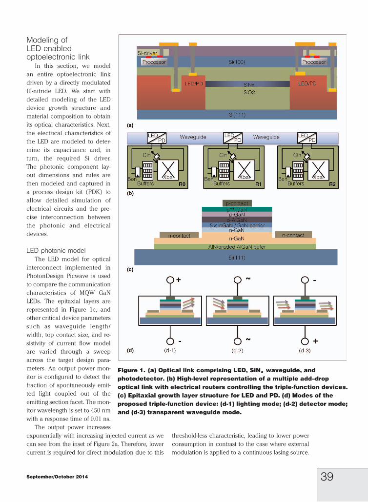
Figure 1a shows an optical link fabricated on the
III-nitride and Si–CMOS-integrated process where
CMOS devices and circuits such as processors (with
associated caches, routers, and link drivers) are
fabricated on a silicon-on-insulator (SOI) wafer and
the III-nitride photonic devices such as LEDs, SiNx
waveguides and photodetectors are processed on
the GaN-on-Si wafer. The add–drop optical link
(Figure 1b) is similar to a conventional electrical
bus. The same III-nitride epitaxial growth layer struc-
ture (Figure 1c) can be employed for achieving
triple-function optoelectronics devices: exhibiting
light-emitting device, photodetector, and transpar-
ent pass-through [8]. This versatility of the device is
attributed to the strong quantum confined Stark
effect (QCSE) in polar (0001) InGaN/GaN multi-
quantum well (MQW), which is as follows: the
bandgap of the material is shifted with applied elec-
tric field and thereby the absorption coefficient ver-
sus wavelength is controlledwith the applied bias [9].
LED. InGaN/GaN MQW LED structures have been
widely used as a solid-state light source. When the
device with the layer structure in Figure 1c is for-
ward biased (Figure 1d-1), light will be generated
and coupled into the waveguide. This integrated
MQW �-LED is specially designed for high-speed on-
chip communication due to microsize effects as well
as a more efficient usage of injected current [3].
Photodetector. After propagating a distance along
this waveguide, the optical signal is coupled into the
same MQW structure as LED, now functioning as a
photodetector absorbing at the LED’s emitting wave-
length (Figure 1d-2). The responsivity of such a
detector is about 0.1 A/W for the peak emission
wavelength [8]. The excess unrecombined electron–
hole pairs can be swept out with fast reverse biasing
for enhanced high-speed response if necessary.
Transparent mode. This device is also capable of
guiding the light through with minimal insertion loss
by reverse biasing. Due to the increased QCSE as a
result of reverse biasing, the overlap between elec-
trons and holes in the MQWs is greatly reduced,
leading to a correspondingly decreased absorption
coefficient and small absorption loss (Figure 1d-3).
Waveguide. SiNx, with refractive index of �2.1 andbandgap of �5 eV, is chosen as the candidate of
waveguide material that is transparent and low
loss (around 1 dB/cm) in the working wavelength
of 450 nm. Due to its high refractive index in con-
trast to SiO2, good light confinement is easily
achieved. Besides, SiON, which is a mixture of SiNx
and SiO2, can supply a tunable refractive index and
transparent wavelength, providing a better freedom
of design. The waveguide, with core size of 360 nm�180 nm, is evaluated using PhotonDesign Firmwave,
showing that confinement for the TE mode is around
96% and the TM mode around 74% for the working
wavelength.
IEEE Design & Test38
Silicon Nanophotonics for Future Multicore Architectures
Modeling ofLED-enabledoptoelectronic link
In this section, we model
an entire optoelectronic link
driven by a directly modulated
III-nitride LED. We start with
detailed modeling of the LED
device growth structure and
material composition to obtain
its optical characteristics. Next,
the electrical characteristics of
the LED are modeled to deter-
mine its capacitance and, in
turn, the required Si driver.
The photonic component lay-
out dimensions and rules are
then modeled and captured in
a process design kit (PDK) to
allow detailed simulation of
electrical circuits and the pre-
cise interconnection between
the photonic and electrical
devices.
LED photonic modelThe LED model for optical
interconnect implemented in
PhotonDesign Picwave is used
to compare the communication
characteristics of MQW GaN
LEDs. The epitaxial layers are
represented in Figure 1c, and
other critical device parameters
such as waveguide length/
width, top contact size, and re-
sistivity of current flow model
are varied through a sweep
across the target design para-
meters. An output power mon-
itor is configured to detect the
fraction of spontaneously emit-
ted light coupled out of the
emitting section facet. The mon-
itor wavelength is set to 450 nm
with a response time of 0.01 ns.
The output power increases
exponentially with increasing injected current as we
can see from the inset of Figure 2a. Therefore, lower
current is required for direct modulation due to this
threshold-less characteristic, leading to lower power
consumption in contrast to the case where external
modulation is applied to a continuous lasing source.
Figure 1. (a) Optical link comprising LED, SiNx waveguide, andphotodetector. (b) High-level representation of a multiple add–dropoptical link with electrical routers controlling the triple-function devices.(c) Epitaxial growth layer structure for LED and PD. (d) Modes of theproposed triple-function device: (d-1) lighting mode; (d-2) detector mode;and (d-3) transparent waveguide mode.
September/October 2014 39
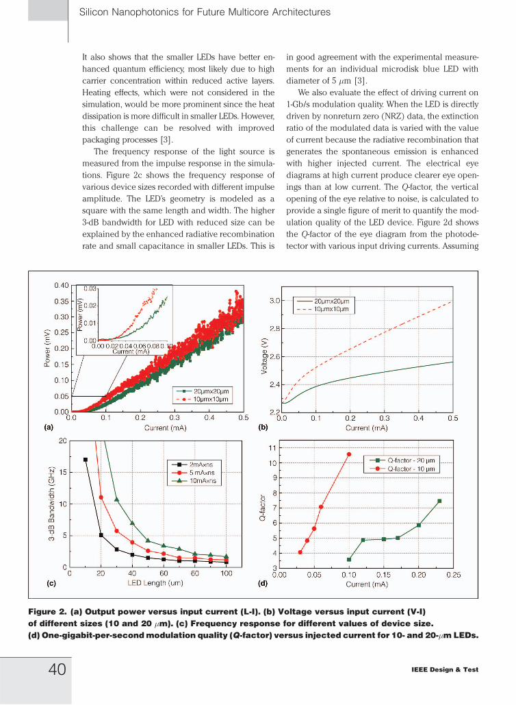
It also shows that the smaller LEDs have better en-
hanced quantum efficiency, most likely due to high
carrier concentration within reduced active layers.
Heating effects, which were not considered in the
simulation, would be more prominent since the heat
dissipation is more difficult in smaller LEDs. However,
this challenge can be resolved with improved
packaging processes [3].
The frequency response of the light source is
measured from the impulse response in the simula-
tions. Figure 2c shows the frequency response of
various device sizes recorded with different impulse
amplitude. The LED’s geometry is modeled as a
square with the same length and width. The higher
3-dB bandwidth for LED with reduced size can be
explained by the enhanced radiative recombination
rate and small capacitance in smaller LEDs. This is
in good agreement with the experimental measure-
ments for an individual microdisk blue LED with
diameter of 5 �m [3].
We also evaluate the effect of driving current on
1-Gb/s modulation quality. When the LED is directly
driven by nonreturn zero (NRZ) data, the extinction
ratio of the modulated data is varied with the value
of current because the radiative recombination that
generates the spontaneous emission is enhanced
with higher injected current. The electrical eye
diagrams at high current produce clearer eye open-
ings than at low current. The Q-factor, the vertical
opening of the eye relative to noise, is calculated to
provide a single figure of merit to quantify the mod-
ulation quality of the LED device. Figure 2d shows
the Q-factor of the eye diagram from the photode-
tector with various input driving currents. Assuming
Figure 2. (a) Output power versus input current (L-I). (b) Voltage versus input current (V-I)of different sizes (10 and 20 �m). (c) Frequency response for different values of device size.(d) One-gigabit-per-secondmodulation quality (Q-factor) versus injected current for 10- and 20-�mLEDs.
IEEE Design & Test40
Silicon Nanophotonics for Future Multicore Architectures
a target bit error rate of 10�9,
similar to that of existing copper
interconnect, a Q ¼ 6 is de-
sired, which translates to driv-
ing currents for 10- and 20-�m
LED of about 0.06 and 0.2 mA
with output power of 30 and
100 �W, respectively.
LED circuit modelA basic LED-equivalent cir-
cuit can consist of a combined
depletion and diffusion capaci-
tance, parallel/serial resistor,
and build-in voltage source.
The capacitance of the LED can be explained by
charge storage during carrier flow. When the LED is
switched on, the depletion capacitance dramatical-
ly reduces and the charges injected into the neutral
region cause diffusion capacitance, which becomes
the dominant factor in the switching speed of the
device. The capacitance can be modeled as
C ¼ A
ffiffiffiffiffiffiffiffiffiffiffiffiffiffiffiffiffiffiffiffiffiffiffiffiffiffiffiffiffiffiffiffiffiffiffiffiffiq"r"0ðND � NAÞ
2 Vbi � V � KT
q
� �vuuut (1)
where A is the LED cross-sectional area, Nd is the
donor concentration, NA is the acceptor concentra-
tion, "r is the permittivity (for GaN, "r ¼ 9:5"0), Vbi is
the built-in potential, and KT=q is the thermal volt-
age. For example, with this model, a 10 � 10-�m2
GaN LED has estimated capacitance of around 6.3 fF.
The device capacitance is critical for determining
the Si-driver size needed to meet the data-rate re-
quirement [1], [10]. The Si driver is modeled as an
inverter chain predriver followed by a final driver
stage, and the energy per bit of the driver can be
calculated as in [10].
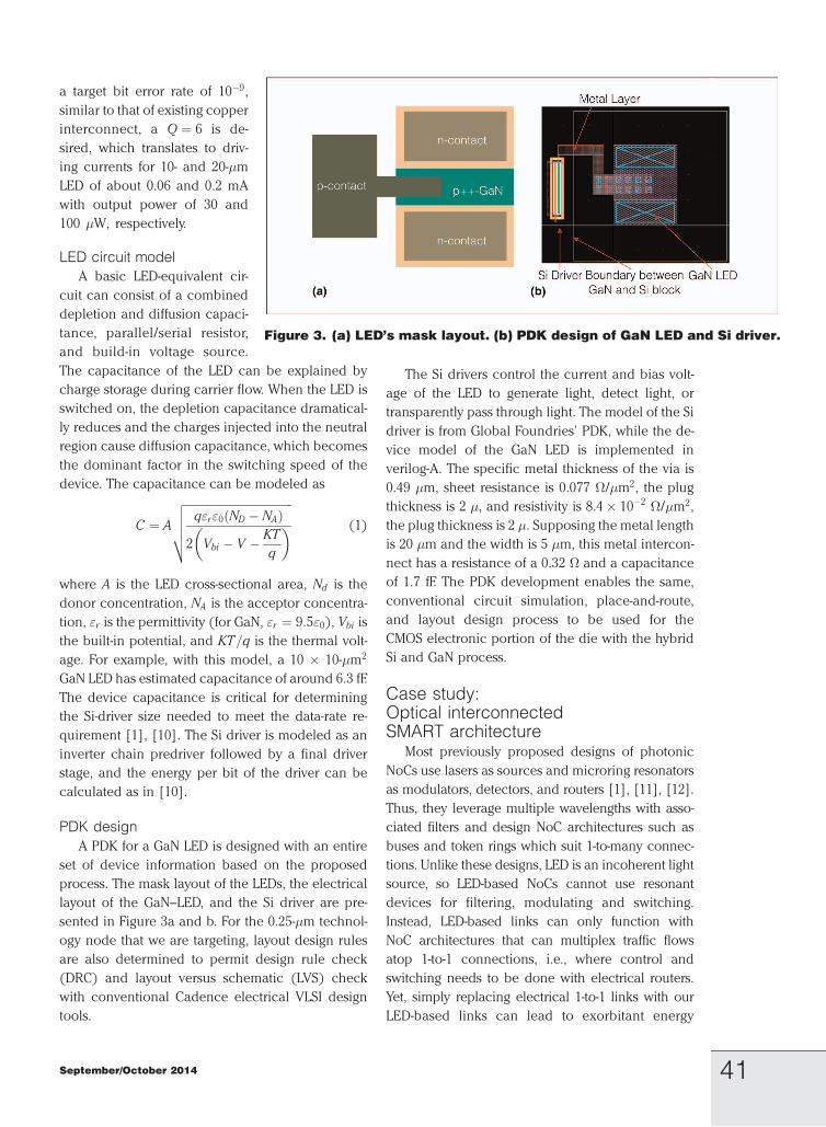
PDK designA PDK for a GaN LED is designed with an entire
set of device information based on the proposed
process. The mask layout of the LEDs, the electrical
layout of the GaN–LED, and the Si driver are pre-
sented in Figure 3a and b. For the 0.25-�m technol-
ogy node that we are targeting, layout design rules
are also determined to permit design rule check
(DRC) and layout versus schematic (LVS) check
with conventional Cadence electrical VLSI design
tools.
The Si drivers control the current and bias volt-
age of the LED to generate light, detect light, or
transparently pass through light. The model of the Si
driver is from Global Foundries’ PDK, while the de-
vice model of the GaN LED is implemented in
verilog-A. The specific metal thickness of the via is
0.49 �m, sheet resistance is 0.077 �/�m2, the plug
thickness is 2 �, and resistivity is 8.4� 10�2 �/�m2,
the plug thickness is 2 �. Supposing the metal length
is 20 �m and the width is 5 �m, this metal intercon-
nect has a resistance of a 0.32 � and a capacitance
of 1.7 fF. The PDK development enables the same,
conventional circuit simulation, place-and-route,
and layout design process to be used for the
CMOS electronic portion of the die with the hybrid
Si and GaN process.
Case study:Optical interconnectedSMART architecture
Most previously proposed designs of photonic
NoCs use lasers as sources and microring resonators
as modulators, detectors, and routers [1], [11], [12].
Thus, they leverage multiple wavelengths with asso-
ciated filters and design NoC architectures such as
buses and token rings which suit 1-to-many connec-
tions. Unlike these designs, LED is an incoherent light
source, so LED-based NoCs cannot use resonant
devices for filtering, modulating and switching.
Instead, LED-based links can only function with
NoC architectures that can multiplex traffic flows
atop 1-to-1 connections, i.e., where control and
switching needs to be done with electrical routers.
Yet, simply replacing electrical 1-to-1 links with our
LED-based links can lead to exorbitant energy
Figure 3. (a) LED’s mask layout. (b) PDK design of GaN LED and Si driver.
September/October 2014 41
consumed in the optical–electrical–optical (O/E/O)
crossings that overwhelm the energy benefits.
Here, we present a case study exploring the suit-
ability of a recently proposed NoC architecture
SMART [7], which was originally architected for
electrical clockless repeated links to realize a single-
cycle data path across the entire die. SMART’s ability
to bypass intermediate routers within the same cycle
allows our LED links to traverse long distances with-
out the unnecessary O/E/O crossings in between,
making the mesh topology feasible for our LED
links. Any other NoC topologies that rely on 1-to-1
connections will also function with our LED links,
but the energy benefits depend on the number of
O/E/O crossings into electrical routers. In LED-enabled
mesh (with SMART) and clos, we compare the NoC
power performance of our LED links within the
SMART mesh as well as a conventional clos topology.
SMART was proposed as a solution to break
the latency barrier for NoCs, but it still consumes
28–32 fJ/b/mm, leading to a worst case transmission
energy of 600 fJ to send a bit from one chip edge to
the other on a typical 20� 20-mm2 chip. We see
the potential of embedding LED-enabled photonic
links into the SMART architecture to further break
the power barrier of on-chip communications.
SMART allows messages to dynamically arbitrate
and create multihop bypass paths across the chip
on-demand over a shared network fabric. Messages
are only buffered at intermediate routers upon
contention. By bypassing intermediate electrical
routers, a message is allowed to transverse from
source to destination electrical routers, avoiding
the high energy overhead of intermediate electri-
cal routers in most cases. Within the LED-enabled
SMART, the electrical links are replaced with the
proposed optical links containing LEDs, wave-
guides, and photodetector (PD), leveraging the
distance-independent low-power transmission of
photonics. SMART is set to prioritize bypassing mes-
sages over incoming ones, i.e., new messages are
not injected into the NoC until existing messages
already in the NoC are drained out. So, a message
usually stays within the photonic plane from source
to turning router, goes through the electrical turning
router, then again zooms through the photonic
plane from the turning to destination router, limiting
the E/O/E. We can take an 8 � 8 optical intercon-
nected mesh SMART NoC as an example: noting
that two optical layers are generated to eliminate
in-plane waveguide crossing loss, each layer con-
taining eight 1 � 8 LED add–drop nodes as shown in
Figure 1b; and optical data are converted to electri-
cal signals in the turning router from one plane to
another. Our III-nitride and Si–CMOS integration
process enables the optical links to be closely integ-
rated with the CMOS routers and processors.
Link energy evaluationWe evaluate the energy efficiency of our LED-
enabled link against a baseline electrical clockless
repeated link in the 45-nm node and a laser-enabled
link using DSENT, a timing-driven NoC power
modeling tool [1]. The laser-enabled optical link is
composed of off-chip laser, microring modulator,
receivers, and peripheral electrical devices. We use
the electrical LED model described in the LED
Circuit Model section to estimate the Si-driver size in
DSENT. In particular, the effective capacitance of
the LED (6.3 fF) and parasitic capacitance of the
vias (1.7 fF) are used to size the driver and its power
consumption. Waveguide loss is set to be 1 dB/cm,
as discussed in the III-nitride and Si–CMOS Opti-
cal Link Design section, and responsivity for the
detector is set to 0.1 A/W. For a short distances
(G 8 mm), most power is consumed by the elec-
trical circuits in the optoelectronic link. Therefore,
it is shown in Figure 4a that the energy for electronic
links increases linearly while the optical links re-
main almost the same regardless of the transmitting
distance. The LED-enabled links outperform other
designs with power efficiency of around 38 fJ/b.
64-core processor simulationsWe run the parallel sections of all 64-threaded
SPLASH-2 applications on an 8 � 8 multicore chip
with shared L2 cache, averaging the multiple ap-
plications’ results. Two electrical NoC baselines are
used: a state-of-the-art NoC with single-cycle-pipeline
routers and a SMART NoC. All results are normalized
against the single-cycle router. Note that both elec-
trical NoC baselines are highly optimized, beating
recent industry chip prototypes such as Intel 48-core
SCC with a three-cycle router in latency and energy.
Performance-wise, the electrical SMART delivers
5–8� lower latency than the single-cycle router elec-
trical baseline, and our photonic SMART NoC main-
tains this performance benefit. Figure 4b graphs the
energy consumption averaged across all SPLASH ap-
plications. The electrical SMART has a slight energy
IEEE Design & Test42
Silicon Nanophotonics for Future Multicore Architectures
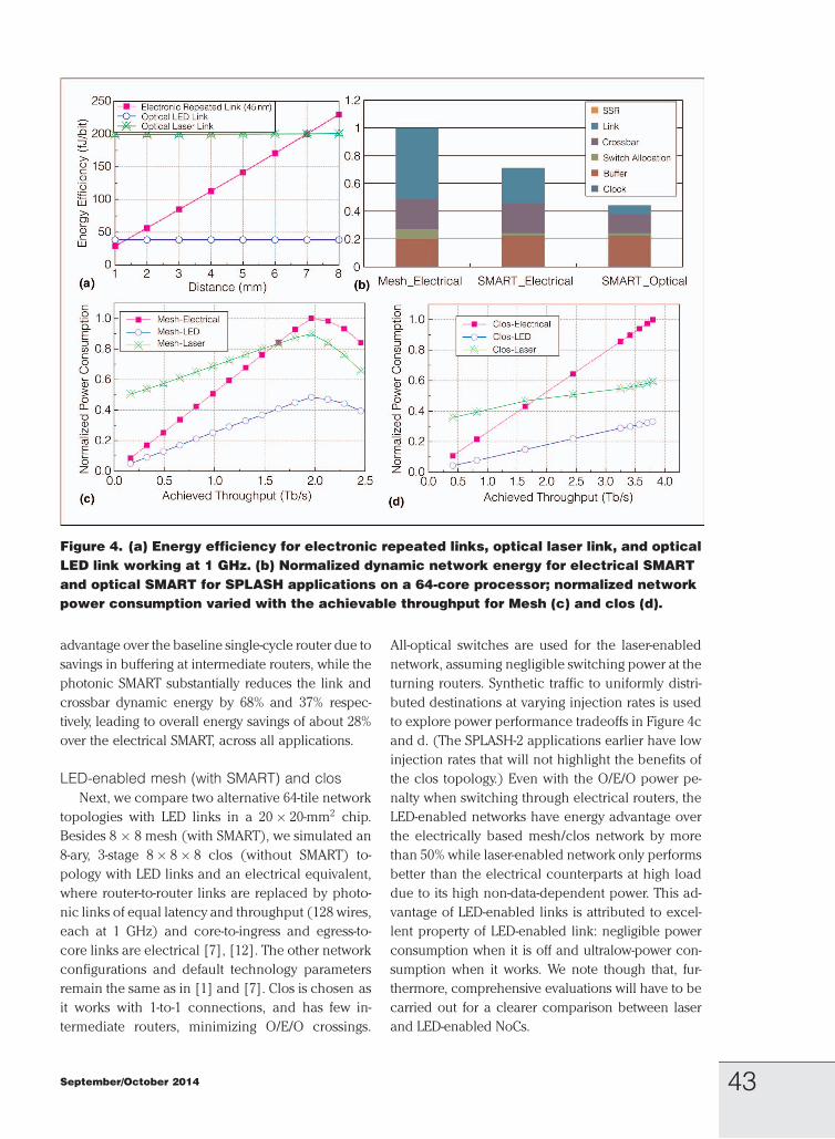
advantage over the baseline single-cycle router due to
savings in buffering at intermediate routers, while the
photonic SMART substantially reduces the link and
crossbar dynamic energy by 68% and 37% respec-
tively, leading to overall energy savings of about 28%
over the electrical SMART, across all applications.
LED-enabled mesh (with SMART) and closNext, we compare two alternative 64-tile network
topologies with LED links in a 20� 20-mm2 chip.
Besides 8 � 8 mesh (with SMART), we simulated an
8-ary, 3-stage 8� 8� 8 clos (without SMART) to-
pology with LED links and an electrical equivalent,
where router-to-router links are replaced by photo-
nic links of equal latency and throughput (128 wires,
each at 1 GHz) and core-to-ingress and egress-to-
core links are electrical [7], [12]. The other network
configurations and default technology parameters
remain the same as in [1] and [7]. Clos is chosen as
it works with 1-to-1 connections, and has few in-
termediate routers, minimizing O/E/O crossings.
All-optical switches are used for the laser-enabled
network, assuming negligible switching power at the
turning routers. Synthetic traffic to uniformly distri-
buted destinations at varying injection rates is used
to explore power performance tradeoffs in Figure 4c
and d. (The SPLASH-2 applications earlier have low
injection rates that will not highlight the benefits of
the clos topology.) Even with the O/E/O power pe-
nalty when switching through electrical routers, the
LED-enabled networks have energy advantage over
the electrically based mesh/clos network by more
than 50% while laser-enabled network only performs
better than the electrical counterparts at high load
due to its high non-data-dependent power. This ad-
vantage of LED-enabled links is attributed to excel-
lent property of LED-enabled link: negligible power
consumption when it is off and ultralow-power con-
sumption when it works. We note though that, fur-
thermore, comprehensive evaluations will have to be
carried out for a clearer comparison between laser
and LED-enabled NoCs.
Figure 4. (a) Energy efficiency for electronic repeated links, optical laser link, and opticalLED link working at 1 GHz. (b) Normalized dynamic network energy for electrical SMARTand optical SMART for SPLASH applications on a 64-core processor; normalized networkpower consumption varied with the achievable throughput for Mesh (c) and clos (d).
September/October 2014 43
WE PROPOSED AN LED-enabled on-chip optical net-
work that leverages a novel III-nitride and Si–CMOS
integrated process. This process allows transistor-
level integration of CMOS circuits and III-nitride
photonic devices, enabling fabrication of a com-
plete optical link on-chip with light sources, wave-
guides, photodetectors, and driving circuits. From
detailed modeling of the LED device growth struc-
ture and material composition, the simulation re-
sults, including output power, frequency response,
and communication quality, are shown to meet the
requirements of on-chip communications. The pho-
tonic component layout dimensions and rules are
also modeled and captured in a PDK, enabling
existing circuit simulation and place-and-route
design flow to continue to be used for the CMOS
electronics portion of the die. We embed our LED-
enabled optical link design into the SMART NoC
architecture, an architecture originally proposed for
electrical interconnects but which is well matched
for the characteristics of our LED-enabled links.
Results from system level simulations of a 64-core
processor show 28% more energy efficiency com-
pared to fully electrical SMART NoC, which already
beats prior electrical designs in energy and delay.
In addition, more than 50% power saving is observed
across the achievable throughput for mesh and clos
topologies. We hope these results based on a col-
laboration with our team members of material, pro-
cess, device, circuit, and architecture researchers
will pave the way for energy-efficient designs of
future on-chip optical communication. We have
since fabricated samples of the proposed LED MQW
structure and are in the midst of testing and
measurements. h
AcknowledgmentWe thank Dr. Z. Liu for detailed discussions re-
garding the material and process, and Dr. T. Krishna
and O. Chen for their assistance with system-level
simulations.
h References[1] C. Sun et al., ‘‘DSENTVA tool connecting emerging
photonics with electronics for opto-electronic
networks-on-chip modeling,’’ in Proc. 6th Int. Symp.
Networks-on-Chip, Lyngby, Denmark, May 2012,
pp. 201–210.
[2] G. Shambat et al., ‘‘Ultrafast direct modulation of a
single-mode photonic crystal nanocavity light-emitting
diode,’’ Nature Commum., vol. 2, 2011, DOI: 10.1038/
ncomms1543.
[3] S. X. Jin, J. Shakya, J. Y. Lin, and H. X. Jiang, ‘‘Size
dependence of III-nitride microdisk light-emitting
diode characteristics,’’ Appl. Phys. Lett., vol. 78,
pp. 3532–3534, 2001.
[4] C. H. Chen et al., ‘‘GHz bandwidth GaAs
light-emitting diodes,’’ Appl. Phys. Lett.
vol. 74, no. 21, pp. 3140–3142, 1999.
[5] Y. Vlasov, ‘‘Silicon photonics for next generation
computing systems,’’ in Proc. 34th Eur. Conf. Exhibit.
Opt. Commun., 2008, DOI: 10.1109/ECOC.2008.
4729553.
[6] J. W. Chung, J. Lee, E. L. Piner, and T. Palacios,
‘‘Seamless on-wafer integration of GaN HEMTs and
Si(100) MOSFETs,’’ IEEE Electron Device Lett.
vol. 30, no. 10, pp. 1015–1017, Jun. 2009.
[7] T. Krishna, C.-H. O. Chen, W. C. Kwon, and
L.-S. Peh, ‘‘Breaking the on-chip latency barrier using
smart,’’ in Proc. 19th Int. Symp. High-Performance
Comput. Architect., Shenzhen, China, Feb. 2013,
pp. 378–389.
[8] Y. D. Jhou et al., ‘‘Nitride-based light emitting diode
and photodetector dual function devices with
InGaN/GaN multiple quantum well structures,’’
Solid-State Electron., vol. 49, pp. 1347–1351, 2005.
[9] C. Rivera, J. L. Pau, F. B. Naranjo, and E. Munoz,
‘‘Novel photodetectors based on InGaN/GaN
multiple quantum wells,’’ Phys. Stat. Sol. A, vol. 201,
pp. 2658–2662, 2004.
[10] M. Georgas, J. Leu, B. Moss, S. Chen, and
V. Stojanovic, ‘‘Addressing link-level design tradeoffs
for integrated photonic interconnects,’’ in Proc. IEEE
Custom Integr. Circuits Conf., 2011, DOI: 10.1109/
CICC.2011.6055363.
[11] A. Shacham, K. Bergman, and L. P. Carloni, ‘‘Photonic
networks-on-chip for future generations of chip
multiprocessors,’’ IEEE Trans. Comput., vol. 57, no. 9,
pp. 1246–1260, Sep. 2008.
[12] A. Joshi et al., ‘‘Silicon-photonic clos networks for
global on-chip communication,’’ in Proc. 3rd Int.
Symp. Network-on-Chip, May 2009, pp. 124–133.
Wenjia Zhang, biography not available at the timeof publication.
Bing Wang, biography not available at the time ofpublication.
IEEE Design & Test44
Silicon Nanophotonics for Future Multicore Architectures

Zhaomin Zhu, biography not available at the timeof publication.
Kenneth Eng Kian Lee, biography not avail-able at the time of publication.
Li Zhang, biography not available at the time ofpublication.
Jurgen Michel, biography not available at thetime of publication.
Li-Shiuan Peh, biography not available at thetime of publication.
Chua Soo-Jin, biography not available at the timeof publication.
h Direct questions and comments about this articleto Wenjia Zhang, Low Energy Electronic Systems(LEES), Singapore-MIT Alliance for Research andTechnology (Smart), Singapore; [email protected].
September/October 2014 45