Embed Size (px)
Citation preview
Role of cation disorder in carrier localization anddensity of states in ZnGeN2
Jacob J. Cordell,∗,†,‡ Garritt J. Tucker,† Adele Tamboli,‡ and Stephan Lany∗,‡
†Department of Mechanical Engineering, Colorado School of Mines, Golden, CO, USA‡Materials Science Center, National Renewable Energy Laboratory, Golden, CO, USA
E-mail: [email protected]; [email protected]
Abstract
Cation site disorder provides a degree of free-dom in the growth of ternary nitrides for tun-ing the technologically relevant properties of amaterial system. For example, the band gap ofZnGeN2 changes when the ordering of the struc-ture deviates from that of its ground state. Bycombining the perspectives of carrier localiza-tion and defect states, we analyze the impactof different degrees of disordering on electronicproperties in ZnGeN2, addressing a gap in cur-rent studies which focus on dilute or fully disor-dered systems. The present study demonstrateschanges in the density of states and localizationof carriers in ZnGeN2 calculated using bandgap-corrected density functional theory and hy-brid calculations on partially disordered super-cells generated using the Monte Carlo method.We use localization and density of states to dis-cuss the ill-defined nature of a band gap in adisordered material, comparing multiple defini-tions of the energy gap in the context of theoryand experiment. Decreasing the order parame-ter results in a large reduction of the band gapin disordered cases. The reduction in band gapis due in part to isolated, localized states thatform above the valence band continuum and areassociated with nitrogen coordinated by morezinc than germanium. The prevalence of defectstates in all but the perfectly ordered structurecreates challenges for incorporating disorderedZnGeN2 into optical devices, but the localiza-tion associated with these defects provides in-
sight into mechanisms of electron/hole recom-bination in the material.
Keywords
site disorder, II IV V2, nitrides, localization
1 Introduction
Site disorder, the replacement of chemicalspecies on a fixed crystallographic lattice, hasrecently grown in interest across semiconductorresearch areas as a means to control optoelec-tronic properties. While site disorder-referredto from here on simply as disorder or degree oforder-has notably been studied as a mechanismfor managing properties in chalcogenide transis-tor and solar cell materials for some time,1–5 itsapplication to such a vast array of ternary andmultinary nitrides and phosphides is a more re-cent development.6,7 Specifically, site disorderhas been investigated as a means of loweringband gaps to ideal ranges for targeted applica-tions. For instance, in ZnGeN2, cation disordermay be able to reduce the band gap from thecalculated8–10 and measured11–14 3.0-3.6 eV tothe 2.1-2.5 eV range desired for amber to greenwavelengths in a light emitting diode (LED),often referred to as the green gap.15 DisorderedZnGeN2, which is lattice matched to GaN, maybe desirable as a replacement for high In con-tent InxGa1−xN, which suffers from a miscibil-ity gap and large lattice mismatch with GaN in
1
arX
iv:2
109.
0506
2v1
[co
nd-m
at.m
trl-
sci]
10
Sep
2021

heterostructure devices.11,16–18
To investigate the impact of disorder on theband gap of ZnGeN2, we utilize disorderedstructures generated from Monte Carlo simula-tion in large supercells of 1,024 atoms.19 Thesestructure models incorporate site disorder con-sisting of cation antisite pairs, which numerousdefect studies have highlighted as the dominantnative defects in ZnGeN2.
8,10,20–25 In contrast toa dilute defect model, site disorder accounts forthe interaction of ZnGe and GeZn present inhigh concentrations representative of materialsgrown under non-equilibrium conditions. Thisstudy separates the impact of site disorder ex-plicitly from stoichiometry, non-native defectsand crystalline quality, all known to further in-fluence optical and electronic properties of in-terest. To illustrate the ordered system, Fig-ure 1 provides the crystal structure, reciprocalspace map and band structure.
Figure 1: a) Ordered ground state crystal struc-ture of ZnGeN2 b) reciprocal space map of Zn-GeN2 (b3 > b2 > b1) c) band structure and DOSof ordered ZnGeN2.
Because disorder adds nuance to how a bandgap is measured and calculated, when the term‘band gap’ is used in this work, we refer to
the energy difference between the highest occu-pied and lowest unoccupied states unless spec-ified otherwise. However, this energy differ-ence is not the only viable definition as willbe discussed throughout this Letter. In a di-lute defect picture, defects do not interact andadditional occupied or unoccupied states areviewed as defect states within an otherwise un-changed band gap. Historically, the theoreti-cal discussion of differentiating band gaps anddefect states has been held in this context ofdilute point defects26–28 or in fully random sys-tems,29–31 but misses systems with intermedi-ate degrees of order with a few notable excep-tions.32,33 In materials with both dilute andnon-dilute defects, Urbach energy34 describeshow the optical absorption of a semiconductortails off exponentially35–37 at energies below theband gap due to transitions from within bandsto defect states in the energy gap and at evenlower energies directly between defect states inthe gap.38–40 Urbach tails are evident in Tauc41
analyses of thin films as well as in bulk sys-tems, where variations of the Kubelka-Munkmethod42,43 are often used to interpret bandgaps. These bulk and film methods frequentlyvary in interpretation of an optical band gapbased on differences in their assumptions.44–46
The difficulty in properly defining a band gapstems to a large extent from the fact that theband gap is used as a scalar metric to addressa multitude of related but distinct phenomenaand questions, either in experimental measure-ments or theoretical computation, and in vari-ous fields of research. Fundamentally, the bandgap is the difference between ionization po-tential (electron removal energy) and electronaffinity (electron addition energy). As such, itis not an optical or even excited-state prop-erty. However, most experimental approachesfor band gap measurements are based on opti-cal spectroscopy, as mentioned above. In suchapproaches, it is difficult to account for nontriv-ial physical mechanisms that modify the shapeof the spectra from which the band gap valueis deduced. For example, calculations using theBethe-Salpeter equation (e.g.,47) show that ex-citonic effects (electron-hole interaction) tendto redshift the dielectric response above the ab-
2

sorption threshold compared to the indepen-dent particle approximation, and enable sub-band gap excitations (exciton binding energy).Similarly, the variation of oscillator strength re-sulting from wavefunction symmetries (directvs indirect, allowed vs forbidden transitions) isoften not precisely known, but can affect thespectra in ways that are not fully captured bymodel parameters used, e.g. in Tauc analysis.Furthermore, there is a fundamental differencebetween optical transition energies in absorp-tion and emission, i.e., the Stokes shift,48 whichis non-radiatively converted to heat. These ef-fects add significant uncertainties to band gapdetermination in all but the most thoroughlycharacterized systems (e.g., GaAs,49 Cu2O,50
ZnO,51 GaN52). These uncertainties are fur-ther exacerbated in disordered materials, whereone must make additional assumptions or definemodels to discriminate between defect and con-tinuum states. This work addresses these chal-lenges from the perspective of large-scale su-percell electronic structure calculations in dis-ordered ZnGeN2.
This Letter builds on results from previouswork19 in which disordered ZnGeN2 structuresin 1,024 atom supercells were generated us-ing Monte Carlo (MC) simulations, providingatomic structure models with systematic varia-tion of the order parameters across the order-disorder transition. The degree of disorderis controlled by an effective temperature de-scribing the site ordering of a cation configu-ration within a crystalline system. This modelincludes the configurational entropy contribu-tion to the free energy of the system, but ex-cludes factors such as decomposition reactionswhich dominate at higher actual synthesis orprocess temperatures. Thus, the effective tem-perature provides a link to map site disorderbetween MC simulations and non-equilibriumsynthesis.19 We focus in this letter on four ef-fective temperatures representing four separateregimes of ordering. 2,000 K and 2,500 K struc-tures include the ground state, ordered configu-ration as well as mostly ordered structures withfew antisites per cell. 3,000 K structures aredisordered, but not random and 5,000 K struc-tures are highly disordered but still not ran-
dom. The level of disorder between 3,000 Kand 5,000 K is best understood through differ-ences in electronic properties as discussed laterin this Letter. Truly random configurations arenot realized below effective temperatures of ap-proximately 400,000 K.19
Both long- (LRO) and short- (SRO) rangeorder parameters–measures of Wyckoff site oc-cupancy and nitrogen coordination, respec-tively–indicate full ordering at low effectivetemperatures. Both parameters slightly de-crease from their ordered values of one whenindividual defect pairs (site exchange of Zn andGe) are introduced in the supercells with in-creasing effective temperature. LRO and SROparameters then drop abruptly at the transitionof 2,525K. Above the transition temperature,the order parameters taper from small valuesto their fully disordered extremes at an infiniteeffective temperature, 0 for LRO and 0.375 forSRO. The transition in order parameters cov-ers a wider range of accessible SRO than LROparameters, but the transition occurs in bothlength scales simultaneously (LRO and SRO arestrongly coupled). This behavior contrasts withthe ZnSnN2:ZnO system,53 where SRO can ex-ist without LRO.
Here, we investigate the electronic structureconsequences from disorder in ZnGeN2 dueto non-equilibrium synthesis. We use non-selfconsistent hybrid functional calculations toenable analysis of the density of states (DOS)and carrier localization as a function of LROand SRO. The band gap of 3.5 eV of orderedZnGeN2 decreases with increasing degree of dis-order and eventually closes for strongly disor-dered configurations. Calculated inverse par-ticipation ratios (IPR) allow us to assess thelocalization of states in this range of disorderedZnGeN2 and discuss how localization impactsour interpretation of a band gap as well as de-vice characteristics. By comparing the DOSof ZnGeN2 structures from band gap correctedcalculations in 1,024 atom cells, we analyze theeffect of disorder on the band gap of the system.
3

2 Disorder and Density of
States
Paying special attention to the role of localizedstates in determining the value of the band gap,we assess what a band gap means in the contextof disordered solids. We use the IPR here as ameasure of the localization of a state at a givenenergy as shown in Equation 1, where the IPRindicates that a given state at a given energy islocalized on average on one out of IPR atoms.An IPR of 1 indicates perfect delocalization anda value of 1,024 indicates exclusive localizationon a single atom within the supercell.
IPR(E) =NA
∑i pi(E)2
[∑
i pi(E)]2(1)
NA is the number of atoms in a supercell andpi(E), the local density of states (LDOS) pro-jected on each atom i as a function of energyE.
To relate DOS, IPR and ordering, we employthe fraction of nitrogen coordinated by exactlytwo Ge and two Zn (Zn2Ge2 motif fraction) as ameasure of SRO, as well as the Bragg-WilliamsLRO parameter, η:
η = rZn + rGe − 1 (2)
where rZn (rGe) is the fraction of Zn (Ge) onZn (Ge) ground state sites.54,55
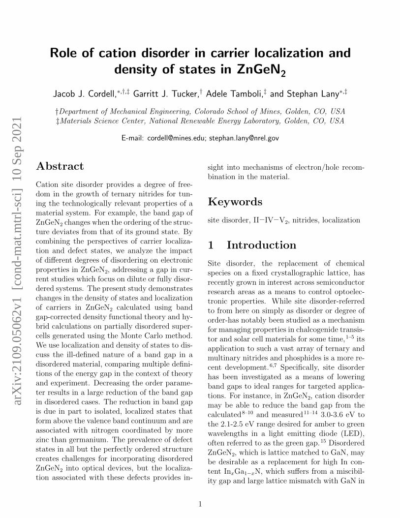
Figure 2a) shows the total DOS of ZnGeN2
configurations grouped by their effective tem-perature and corresponding range of the LROparameter. To access the effect of disorderon valence (occupied) and conduction (unoccu-pied) band states individually, we determinedthe potential alignment of the disordered struc-tures relative to the ground state (see Supple-mental Information). Using a 10 meV incre-ment in data points, defect states appear inthe DOS of disordered structures representedby allowed (non-gray) bands separated from theband edges by forbidden (gray) states. Up toTeff = 2,000 K, the MC simulation largely re-tains the ordered ground state structure, butis starting to develop some ZnGe and GeZn
antisite configurations. Between 2,000 K and2,500 K, the concentration of antisite defects
increases with a concomitant decrease in theband gap by about 0.7 eV. Just above 2,500 K,the system undergoes an order-disorder phasetransition,19 assuming a state with both long-and short-range disorder. It is important tonote, however, that the system retains a sig-nificant degree of non-random LRO and SROup to much higher effective temperatures. Asseen in Figure 2, comparing Teff = 2,500 K and3,000 K, the phase transition is accompaniedby a large reduction of the order parameter ηand an additional band gap reduction of about1.1 eV. The average band gap then decreasesby 1.0 eV from 3,000 K to 5,000 K as the sys-tem tends toward metallic for mostly disorderedstructures.
The decrease in band gap with disorder comesfrom movement in both the conduction bandminimum (CBM) and valence band maximum(VBM); replacing a single pair of cations inthe ground state structure with an antisite pairraises the Fermi level by 200-500 meV depend-ing on the proximity of the pair. The Fermilevel in this context is taken as the midpointbetween the energy levels of the highest oc-cupied and lowest unoccupied states and liesjust below 2 eV on the energy scale of Figure2. Further decreasing the degree of order doesnot significantly impact the Fermi level beyondthe initial shift until the band gap effectivelycloses. Without contributions from non-native,non-antisite defects and stoichiometry, site dis-order alone drastically changes the band gap ofZnGeN2 over a 3.5 eV range.
Figure 2b) provides the corresponding IPR ofthe DOS from Figure 2a) allowing a look at thelocalization of states. IPR is undefined wherethe DOS is zero (in the band gap). Like theDOS, IPR are discretized with a step size of 10meV. The scaling of the color bar representingIPR in Figure 2b) highlights the most localizedstates, the movement of which can be trackedacross the band gap (gray region). These lo-calized states remain relatively constant in en-ergy relative to the VBM but increase in quan-tity and density with decreasing degree of or-der. The localized, mid-gap states indicate ahigh probability of non-radiative recombinationcenters in disordered ZnGeN2,
56,57 which would
4
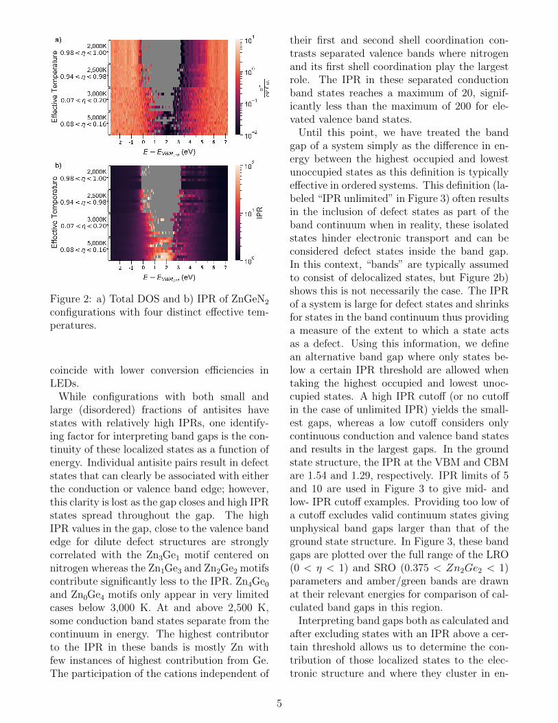
Figure 2: a) Total DOS and b) IPR of ZnGeN2
configurations with four distinct effective tem-peratures.
coincide with lower conversion efficiencies inLEDs.
While configurations with both small andlarge (disordered) fractions of antisites havestates with relatively high IPRs, one identify-ing factor for interpreting band gaps is the con-tinuity of these localized states as a function ofenergy. Individual antisite pairs result in defectstates that can clearly be associated with eitherthe conduction or valence band edge; however,this clarity is lost as the gap closes and high IPRstates spread throughout the gap. The highIPR values in the gap, close to the valence bandedge for dilute defect structures are stronglycorrelated with the Zn3Ge1 motif centered onnitrogen whereas the Zn1Ge3 and Zn2Ge2 motifscontribute significantly less to the IPR. Zn4Ge0and Zn0Ge4 motifs only appear in very limitedcases below 3,000 K. At and above 2,500 K,some conduction band states separate from thecontinuum in energy. The highest contributorto the IPR in these bands is mostly Zn withfew instances of highest contribution from Ge.The participation of the cations independent of
their first and second shell coordination con-trasts separated valence bands where nitrogenand its first shell coordination play the largestrole. The IPR in these separated conductionband states reaches a maximum of 20, signif-icantly less than the maximum of 200 for ele-vated valence band states.
Until this point, we have treated the bandgap of a system simply as the difference in en-ergy between the highest occupied and lowestunoccupied states as this definition is typicallyeffective in ordered systems. This definition (la-beled “IPR unlimited” in Figure 3) often resultsin the inclusion of defect states as part of theband continuum when in reality, these isolatedstates hinder electronic transport and can beconsidered defect states inside the band gap.In this context, “bands” are typically assumedto consist of delocalized states, but Figure 2b)shows this is not necessarily the case. The IPRof a system is large for defect states and shrinksfor states in the band continuum thus providinga measure of the extent to which a state actsas a defect. Using this information, we definean alternative band gap where only states be-low a certain IPR threshold are allowed whentaking the highest occupied and lowest unoc-cupied states. A high IPR cutoff (or no cutoffin the case of unlimited IPR) yields the small-est gaps, whereas a low cutoff considers onlycontinuous conduction and valence band statesand results in the largest gaps. In the groundstate structure, the IPR at the VBM and CBMare 1.54 and 1.29, respectively. IPR limits of 5and 10 are used in Figure 3 to give mid- andlow- IPR cutoff examples. Providing too low ofa cutoff excludes valid continuum states givingunphysical band gaps larger than that of theground state structure. In Figure 3, these bandgaps are plotted over the full range of the LRO(0 < η < 1) and SRO (0.375 < Zn2Ge2 < 1)parameters and amber/green bands are drawnat their relevant energies for comparison of cal-culated band gaps in this region.
Interpreting band gaps both as calculated andafter excluding states with an IPR above a cer-tain threshold allows us to determine the con-tribution of those localized states to the elec-tronic structure and where they cluster in en-
5
Figure 3: Band gap energy as a function of a)long-range order and b) short-range order forthree interpretations of the band gap. IPR un-limited: difference in energy between highestoccupied and lowest unoccupied molecular or-bitals. IPR < 10 (5): States with IPR > 10 (5)are excluded from the band gap determination.
ergy. In Figure 3, the unlimited IPR definitionshows how small fractions of defects drasticallyreduce the band gap, while ignoring highly lo-calized states shows that this significant changeis largely–but not exclusively–due to these iso-lated defects. In the band gap interpretationsthat do not consider highly localized states(e.g., IPR<10 and IPR<5), the band gap stillreduces by roughly 2 eV, but this reductionoccurs through continuous bands in energy indisordered configurations rather than throughdefect states in structures with near-perfect or-dering.
Taking band gaps as the difference between
highest occupied and lowest unoccupied statesyields a change from 3.5 eV to 2.0 eV withonly a drop in LRO parameter from η=1.00 toη=0.94. For low order parameters, the differ-ence between the unlimited gaps and gaps ex-cluding states with IPR>5 is again significant.The IPR limitation places the gap in the am-ber/green region of the visible spectrum withsome trend toward higher band gap with higherSRO parameter per Figure 3b). For largely dis-ordered structures, this sizable transition cre-ates very small band gaps less than 1.6 eV forη ≤ 0.20, a much larger change in band gapwith ordering than predicted for the more re-searched Cu2ZnSnS (CZTS) system.58,59 Whenthese structures are fully random (i.e., at infi-nite effective temperature), the band gaps con-sistently drop to zero for the unlimited defini-tion and remain undefined for the cases withlimited IPR.
Though the supercell size of structures usedfor the present analysis is large for typical DFTcalculations (and especially so for band gap cor-rected electronic structure calculations), it isstill limited in capturing the statistics of con-figurational disorder, particularly in the dilutedefect limit (low effective temperature). Thelocalization of these states in structures withsmall fractions of defects and the impact ofthe defects’ spatial proximity were studied bySkachkov et al.20 These mid-gap states isolatedin energy are generally accepted as detrimentalto optoelectronic properties by decreasing thequantity of carriers collected, reducing the life-times of those carriers or inhibiting radiation ofa photon.60,61 However, at higher defect concen-trations, where defect bands widen in energy asin largely disordered supercells in Figure 2b),conflicting theories exist as to the impact of de-fect density on the relative rate of non-radiativerecombination.
In one theory, Luque et al. directly con-nect non-radiative Shockley-Read-Hall recom-bination to the localization caused by a lowdensity or irregularity of impurities within alattice, but see a reduction in non-radiative re-combination as defect density increases above acertain threshold.62 In this theory, lower den-sities of defects correspond to more spatially
6
isolated and therefore localized defects and spa-tially connected states exhibit more benign elec-tronic properties.63 However, gap states in 2b)show a comparable maximum IPR for everystructure other than the ground state, indepen-dent of the degree of disorder of those configu-rations. These comparable degrees of localiza-tion independent of defect density align betterwith prevalent studies in the InGaN2 system. InInGaN2 and similar III-V alloys, higher defectdensities and deep gap states cause higher ratesof non-radiative recombination.64–66 Based onthe high degree of localization in disorderedconfigurations, this latter theory of higher de-fect densities negatively impacting radiative re-combination applies to ZnGeN2 as well.
3 Conclusion
In this work we examined the effect of cationdisorder on the density and localization of elec-tronic states in ZnGeN2. From non-dilute, dis-ordered, but non-random structures with a sig-nificant degree of SRO, we calculated the DOSand the IPR of the material as a function ofLRO and SRO, extracting band gaps as a func-tion of both order parameters. We discussed theproblem of defining the band gap in disorderedmaterials and the ambiguities associated withthe differentiation between defects and bandstates. While the topic deserves further dis-cussion in the community, we used the IPR asa variable threshold for this separation.
The band gap of the system decreases signifi-cantly with decreasing degree of order from 3.5eV for an ordered system to effectively 0 eVfor strongly disordered systems. This sizablechange in the gap raises the question of howwe differentiate band gaps and defect levels indisordered solids as the gap-closing states arehighly localized. To address this question, weevaluated the band gaps as a function of a local-ization threshold above which states are classi-fied as defect rather than band states.
Localized, occupied states are caused by Nwith Zn-rich coordination. Isolated conductionband states attributed to cations are much lesslocalized and occur independent of the cations’
second shell coordination environment. Ourfindings in ZnGeN2 show a strong tendencyfor localized defect states to form at all or-der parameters other than the ground state,which could detrimentally impact carrier re-combination in a ZnGeN2-based device. Thisresult indicates that SRO is important for in-hibiting carrier localization, which corroboratesrecent findings in ZnSnN2:ZnO with perfectSRO.53 Whereas in ZnSnN2:ZnO, this perfectSRO phase can exist with long-range disorder,the direct relationship between SRO and LROin ZnGeN2 means that both SRO and LROare needed to minimize localization and non-radiative recombination in this system.
4 Electronic structure cal-
culation methods
Data presented in this Letter utilize the atomicconfigurations of19 to predict electronic struc-ture properties as a function of the order param-eter and effective temperature. In Figure 1, theelectronic structure and density of states of Zn-GeN2 were calculated in density functional the-ory (DFT) with band edge corrections to matchthe band gap from GW calculations (3.63 eV8)and plotted using pymatgen.67 To relax the lat-tice parameters, volume and ion positions ofthe 1,024 atom configurations from MC sim-ulations, we used the generalized gradient ap-proximation (GGA), Perdew-Burke-Ernzerhof(PBE)68 type. Due to the large size of thesupercells, a single k-point (1x1x1 mesh) suf-ficed for the relaxation using the gamma-point-only version of the Vienna Ab-initio Simula-tion Package (VASP). These calculations relyon Kresse-Joubert projector augmented wavedatasets with pseudopotentials from VASP ver-sion 4.6 (i.e., Ge d, N s and Zn). The soft pseu-dopotential, N s, allows for a low energy cutoffof 380 eV that benefits the feasibility of cal-culations using large supercells.69 Each super-cell achieved convergence when the differencein energy between steps of the ionic relaxationdropped below 10−5 eV and forces below 0.02
eV �A−1on each atom. These calculations used
a Coulomb potential, U − J = 6 eV, applied
7

to the Zn d orbital following the Dudarev ap-proach.70
The large size of the supercells precludes thepossibility of applying the GW approach71 foreach structure. In place of GW methods, theDOS and IPR of relaxed structures were calcu-lated using a parameterized single-shot hybridfunctional with an additional Coulomb poten-tial V (SSH+V) of -1.5 eV (comparable to a Uparameter of +3 eV) applied to Zn d orbitals.72
The single-shot functional avoids the computa-tionally expensive iteration to self-consistencyof the hybrid functional Hamiltonian by holdingthe initial wavefunctions of the DFT+U calcu-lation fixed.72 This non-self consistent approachdoes not reorient band positions from the priorDFT+U step so in cases where DFT+U-whichdrastically underestimates band gaps-results inno band gap, an additional step was run usingVASP’s ”none” algorithm to renumber bands.This extra step was needed for most 5,000 Kconfigurations and leads to larger uncertaintyin band gaps under 1 eV than other gaps pre-sented in this Letter. The Hartree-Fock ex-change mixing parameter of the SSH+V func-tional was set to 0.19 and screening parameterto 0 for all structures. These parameters werefitted to replicate the total DOS produced byGW calculations for the ground state structurewith a band gap of 3.5 eV calculated in SSH+V.
To align potentials for the purpose of com-paring the DOS and IPR of various disorderedconfigurations on a common energy axis, a po-tential alignment was performed for the volumerelaxed supercells, as described further in theSupplemental Information. Disordered cells areslightly larger than the ground state structurewith a maximum difference in volume of 0.9%for the most disordered supercells described inthis study compared to the ground state super-cell.
Acknowledgement This work was sup-ported by the U.S. Department of Energy(DOE) under Contract No. DE-AC36-08GO28308 with the Alliance for SustainableEnergy, LLC, the manager and operator of theNational Renewable Energy Laboratory. Fund-ing was provided by the U.S. Department of
Energy, Office of Energy Efficiency and Re-newable Energy, Buildings Technologies Office.This work used high-performance computingresources located at NREL and sponsored bythe Office of Energy Efficiency and RenewableEnergy. The views expressed in the paper donot necessarily represent the views of the DOEor the U.S. government. The U.S. governmentretains and the publisher, by accepting the ar-ticle for publication, acknowledges that the U.S. government retains a nonexclusive, paid-up,irrevocable, worldwide license to publish or re-produce the published form of this work, orallow others to do so, for government purposes.
Supporting Information Avail-
able
Tabulated band gaps and maximum IPR valuesused in figures, averaged DOS for each effectivetemperature simulated and potential alignmentused for disordered ZnGeN2.
References
(1) Farges, F.; Brown, G. E.; Rehr, J., et al. TiK-edge XANES studies of Ti coordinationand disorder in oxide compounds: Com-parison between theory and experiment.Physical Review B 1997, 56, 1809.
(2) Ahmed, E.; Hill, A.; D Pilkington, R.;D Tomlinson, R.; Leppavuori, J.; Lev-oska, J.; Kusmartseva, O.; Ahmed, W.;Afzal, A. Deposition and characterizationof copper indium gallium diselenide filmsby laser ablation and flash evaporation foruse in solar cells. Journal of materials sci-ence 1997, 32, 5611–5613.
(3) Martins, R.; Barquinha, P.; Ferreira, I.;Pereira, L.; Goncalves, G.; Fortunato, E.Role of order and disorder on the elec-tronic performances of oxide semiconduc-tor thin film transistors. Journal of appliedphysics 2007, 101, 044505.
(4) Katagiri, H.; Jimbo, K.; Yamada, S.;Kamimura, T.; Maw, W. S.; Fukano, T.;
8

Ito, T.; Motohiro, T. Enhanced conversionefficiencies of Cu2ZnSnS4-based thin filmsolar cells by using preferential etchingtechnique. Applied physics express 2008,1, 041201.
(5) Chen, S.; Gong, X.; Walsh, A.; Wei, S.-H. Crystal and electronic band structureof Cu2ZnSnX4 (X=S and Se) photovoltaicabsorbers: First-principles insights. Ap-plied Physics Letters 2009, 94, 041903.
(6) Schnepf, R. R.; Cordell, J. J.;Tellekamp, M. B.; Melamed, C. L.; Green-away, A. L.; Mis, A.; Brennecka, G. L.;Christensen, S.; Tucker, G. J.; To-berer, E. S., et al. Utilizing site disorderin the development of new energy-relevant semiconductors. ACS EnergyLetters 2020, 5, 2027–2041.
(7) Ogura, M.; Han, D.; Pointner, M. M.;Junkers, L. S.; Rudel, S. S.; Schnick, W.;Ebert, H. Electronic properties of semi-conducting Zn(Si,Ge,Sn)N2 alloys. Phys-ical Review Materials 2021, 5, 024601.
(8) Melamed, C. L.; Pan, J.; Mis, A.; Hein-selman, K.; Schnepf, R. R.; Woods-Robinson, R.; Cordell, J.; Lany, S.; To-berer, E.; Tamboli, A. C. Combinato-rial investigation of structural and opticalproperties of cation-disordered ZnGeN2.Journal of Materials Chemistry C 2020,
(9) Punya, A.; Lambrecht, W. R. L. Quasipar-ticle band structure of Zn IV N2 com-pounds. Physical Review B 2011, 84,165204.
(10) Adamski, N. L.; Zhu, Z.; Wickrama-ratne, D.; Van de Walle, C. G. Hybridfunctional study of native point defectsand impurities in ZnGeN2. Journal of Ap-plied Physics 2017, 122, 195701.
(11) Kikkawa, S.; Morisaka, H. RF-sputter de-position of Zn–Ge nitride thin films. Solidstate communications 1999, 112, 513–515.
(12) Du, K.; Bekele, C.; Hayman, C. C.; An-gus, J. C.; Pirouz, P.; Kash, K.; Kash, . K.Synthesis and characterization of ZnGeN2
grown from elemental Zn and Ge sources.Journal of Crystal Growth 2008, 310,1057–1061.
(13) Osinsky, A.; Fuflyigin, V.; Zhu, L.;Goulakov, A.; Graff, J.; Schubert, E. Newconcepts and preliminary results for SiCbipolar transistors: ZnSiN2 and ZnGeN2
heterojunction emitters. Proceedings 2000IEEE/Cornell Conference on High Per-formance Devices (Cat. No. 00CH37122).2000; pp 168–172.
(14) Viennois, R.; Taliercio, T.; Potin, V.;Errebbahi, A.; Gil, B.; Charar, S.;Haidoux, A.; Tedenac, J.-C. Prospectiveinvestigations of orthorhombic ZnGeN2:synthesis, lattice dynamics and opticalproperties. Materials Science and Engi-neering: B 2001, 82, 45–49.
(15) Phillips, J.; Burrows, P.; Davis, R.; Sim-mons, J.; Malliaras, G.; So, F.; Mis-ewich, J.; Nurmikko, A.; Smith, D.;Tsao, J., et al. Basic Research Needs forSolid-State Lighting. Report of the BasicEnergy Sciences Workshop on Solid-StateLighting, May 22-24, 2006 ; 2006.
(16) Pattison, M.; Hansen, M.; Bardsley, N.;Elliott, C.; Lee, K.; Pattison, L.; Tsao, J.2019 Lighting R&D Opportunities .
(17) Tellekamp, M. B.; Melamed, C. L.; Nor-man, A. G.; Tamboli, A. Heteroepitax-ial integration of ZnGeN2 on GaN buffersusing molecular beam epitaxy. CrystalGrowth & Design 2020, 20, 1868–1875.
(18) Reeber, R. R.; Wang, K. Lattice parame-ters and thermal expansion of GaN. Jour-nal of Materials Research 2000, 15, 40–44.
(19) Cordell, J. J.; Pan, J.; Tamboli, A. C.;Tucker, G. J.; Lany, S. Probing configu-rational disorder in ZnGeN2 using cluster-based Monte Carlo. Physical Review Ma-terials 2021, 5, 024604.
9

(20) Skachkov, D.; Quayle, P. C.; Kash, K.;Lambrecht, W. R. Disorder effects on theband structure of ZnGeN2: Role of ex-change defects. Physical Review B 2016,94, 205201.
(21) Skachkov, D.; Punya Jaroenjittichai, A.;Huang, L.-y.; L Lambrecht, W. R. Nativepoint defects and doping in ZnGeN2. Phys-ical Review B 2016, 93, 155202.
(22) Skachkov, D.; Lambrecht, W. R. L. Na-tive interstitial defects in ZnGeN2. Physi-cal Review Materials 2017, 1, 054604.
(23) Lyu, S.; Skachkov, D.; Kash, K.; Blan-ton, E. W.; Lambrecht, W. R. L. BandGaps, Band-Offsets, Disorder, StabilityRegion, and Point Defects in II-IV-N2
Semiconductors. Physica Status Solidi (a)2019, 216, 1800875.
(24) Skachkov, D.; Lambrecht, W. R. Candi-dates for p-Type doping of ZnGeN2. Jour-nal of Applied Physics 2020, 127 .
(25) Haseman, M. S.; Karim, M. R.;Ramdin, D.; Noesges, B. A.; Feinberg, E.;Jayatunga, B. H. D.; Lambrecht, W.R. L.; Zhu, M.; Hwang, J.; Kash, K.;Zhao, H.; Brillson, L. J. Deep level defectsand cation sublattice disorder in ZnGeN2.Journal of Applied Physics 2020, 127,135703.
(26) Noda, S.; Chutinan, A.; Imada, M. Trap-ping and emission of photons by a singledefect in a photonic bandgap structure.nature 2000, 407, 608–610.
(27) Lany, S.; Zunger, A. Dopability, intrin-sic conductivity, and nonstoichiometry oftransparent conducting oxides. PhysicalReview Letters 2007, 98, 045501.
(28) Freysoldt, C.; Grabowski, B.; Hickel, T.;Neugebauer, J.; Kresse, G.; Janotti, A.;Van de Walle, C. G. First-principles calcu-lations for point defects in solids. Reviewsof modern physics 2014, 86, 253.
(29) Wei, S.-H.; Zunger, A. Band-gap narrow-ing in ordered and disordered semiconduc-tor alloys. Applied physics letters 1990,56, 662–664.
(30) Veal, T. D.; Feldberg, N.; Quacken-bush, N. F.; Linhart, W. M.; Scan-lon, D. O.; Piper, L. F.; Durbin, S. M.Band gap dependence on cation disorderin ZnSnN2 solar absorber. Advanced En-ergy Materials 2015, 5, 1501462.
(31) Xiang, H.; Wei, S.-H.; Da Silva, J. L.;Li, J. Strain relaxation and band-gaptunability in ternary In x Ga 1- x Nnanowires. Physical Review B 2008, 78,193301.
(32) Chan, J.; Liu, J.; Zunger, A. Bridging thegap between atomic microstructure andelectronic properties of alloys: The caseof (In, Ga) N. Physical Review B 2010,82, 045112.
(33) Liu, J.; Fernandez-Serra, M. V.;Allen, P. B. Special quasiordered struc-tures: role of short-range order in thesemiconductor alloy (GaN) 1- x (ZnO) x.Physical Review B 2016, 93, 054207.
(34) Urbach, F. The long-wavelength edge ofphotographic sensitivity and of the elec-tronic Absorption of Solids. Physical Re-view 1953, 92, 1324.
(35) Soukoulis, C. M.; Cohen, M. H.;Economou, E. N. Exponential BandTails in Random Systems. PhysicalReview Letters 1984, 53, 616–619.
(36) John, S.; Soukoulis, C.; Cohen, M. H.;Economou, E. N. Theory of electron bandtails and the urbach optical-absorptionedge. Physical Review Letters 1986, 57,1777–1780.
(37) Sa-Yakant, V.; Glyde, H. R. Urbach Tailsand Disorder. Comments Condensed Mat-ter Physics 1987, 13, 35–48.
(38) Shimakawa, K.; Singh, J.; O’Leary, S. K.Optical Properties of Condensed Matter
10

and Applications ; John Wiley & Sons,Ltd, 2006; Chapter 3, pp 47–62.
(39) Adachi, S. Optical properties of crystallineand amorphous semiconductors: Materi-als and fundamental principles ; SpringerScience & Business Media, 2012.
(40) Sharma, N. Optical band-gap and associ-ated Urbach energy tails in defected AlNthin films grown by ion beam sputter de-position: Effect of assisted ion energyOp-tical band-gap and associated Urbach en-ergy tails in defected AlN thin films grownby ion beam sputter depo. Advanced Ma-terials Proceedings 2017, 2, 342–346.
(41) Tauc, J.; Grigorovici, R.; Vancu, A. Op-tical properties and electronic structureof amorphous germanium. Physica StatusSolidi (b) 1966, 15, 627–637.
(42) Kubelka, P.; Munk, F. An article on opticsof paint layers. Zeitschrift fur TechnischePhysik 1931, 12, 259–274.
(43) Kubelka, P. New contributions to the op-tics of intensely light-scattering materials.Part I. Journal of the Optical Society ofAmerica 1948, 38, 448–457.
(44) Saenz-Trevizo, A.; Amezaga-Madrid, P.;Piza-Ruiz, P.; Antunez-Flores, W.; Miki-Yoshida, M. Optical band gap estima-tion of ZnO nanorods. Materials Research2016, 19, 33–38.
(45) Dolgonos, A.; Mason, T. O.; Poep-pelmeier, K. R. Direct optical band gapmeasurement in polycrystalline semicon-ductors: A critical look at the Taucmethod. Journal of solid state chemistry2016, 240, 43–48.
(46) Maku la, P.; Pacia, M.; Macyk, W. HowTo Correctly Determine the Band GapEnergy of Modified Semiconductor Pho-tocatalysts Based on UV–Vis Spectra.The Journal of Physical Chemistry Letters2018, 9, 6814–6817.
(47) Laskowski, R.; Christensen, N. E.;Santi, G.; Ambrosch-Draxl, C. Ab ini-tio calculations of excitons in GaN. Phys.Rev. B 2005, 72, 035204.
(48) O’Donnell, K. P.; Martin, R. W.; Middle-ton, P. G. Origin of Luminescence fromInGaN Diodes. Phys. Rev. Lett. 1999, 82,237–240.
(49) Nam, S. B.; Reynolds, D. C.; Lit-ton, C. W.; Almassy, R. J.; Collins, T. C.;Wolfe, C. M. Free-exciton energy spec-trum in GaAs. Phys. Rev. B 1976, 13,761–767.
(50) Kazimierczuk, T.; Frohlich, D.; Scheel, S.;Stolz, H.; Bayer, M. Giant Rydberg exci-tons in the copper oxide Cu 2 O. Nature2014, 514, 343–347.
(51) Manjon, F.; Mollar, M.; Hernandez-Fenollosa, M.; Marı, B.; Lauck, R.; Car-dona, M. Effect of isotopic mass on thephotoluminescence spectra of zinc oxide.Solid State Communications 2003, 128,35–39.
(52) Monemar, B. Fundamental energy gap ofGaN from photoluminescence excitationspectra. Phys. Rev. B 1974, 10, 676–681.
(53) Pan, J.; Cordell, J. J.; Tucker, G. J.; Za-kutayev, A.; Tamboli, A. C.; Lany, S.Perfect short-range ordered alloy withline-compound-like properties in the Zn-SnN2:ZnO system. npj ComputationalMaterials 2020, 6, 1–6.
(54) Bragg, W. L.; Williams, E. J. The effect ofthermal agitation on atomic arrangementin alloys. Proceedings of the Royal Societyof London. Series A, Containing Papersof a Mathematical and Physical Character1934, 145, 699–730.
(55) Bragg, W. L.; Williams, E. J. The effect ofthermal agitation on atomic arrangementin alloys—II. Proceedings of the Royal So-ciety of London. Series A-Mathematicaland Physical Sciences 1935, 151, 540–566.
11
(56) Street, R. Non-radiative recombination inchalcogenide glasses. Solid state communi-cations 1977, 24, 363–365.
(57) Kawakami, Y.; Omae, K.; Kaneta, A.;Okamoto, K.; Izumi, T.; Sajou, S.;Inoue, K.; Narukawa, Y.; Mukai, T.;Fujita, S. Radiative and NonradiativeRecombination Processes in GaN-BasedSemiconductors. Physica Status Solidi (a)2001, 183, 41–50.
(58) Scragg, J. J.; Larsen, J. K.; Kumar, M.;Persson, C.; Sendler, J.; Siebentritt, S.;Platzer Bjorkman, C. Cu-Zn disorder andband gap fluctuations in Cu2ZnSn(S,Se)4:Theoretical and experimental investiga-tions. Physica Status Solidi (b) 2016, 253,247–254.
(59) Zawadzki, P.; Zakutayev, A.; Lany, S.Entropy-driven clustering in tetrahedrallybonded multinary materials. Physical Re-view Applied 2015, 3, 034007.
(60) Park, J. S.; Kim, S.; Xie, Z.; Walsh, A.Point defect engineering in thin-film solarcells. Nature Reviews Materials 2018, 3,194–210.
(61) Meneghini, M.; La Grassa, M.; Vac-cari, S.; Galler, B.; Zeisel, R.; Drechsel, P.;Hahn, B.; Meneghesso, G.; Zanoni, E.Characterization of the deep levels re-sponsible for non-radiative recombinationin InGaN/GaN light-emitting diodes. Ap-plied Physics Letters 2014, 104, 113505.
(62) Luque, A.; Martı, A.; Antolın, E.;Tablero, C. Intermediate bands versus lev-els in non-radiative recombination. Phys-ica B: Condensed Matter 2006, 382, 320–327.
(63) Luque, A.; Martı, A.; Stanley, C. Un-derstanding intermediate-band solar cells.Nature Photonics 2012, 6, 146.
(64) Yang, J.-H.; Shi, L.; Wang, L.-W.; Wei, S.-H. Non-radiative carrier recombination
enhanced by two-level process: a first-principles study. Scientific reports 2016,6, 1–10.
(65) Lee, I.-H.; Polyakov, A.; Smirnov, N.;Shchemerov, I.; Lagov, P.; Zinov’Ev, R.;Yakimov, E.; Shcherbachev, K.;Pearton, S. Point defects controllingnon-radiative recombination in GaNblue light emitting diodes: Insights fromradiation damage experiments. Journal ofApplied Physics 2017, 122, 115704.
(66) Shabunina, E.; Averkiev, N.;Chernyakov, A.; Levinshtein, M.;Petrov, P.; Shmidt, N. Extended defectsystem as a main source of non-radiativerecombination in InGaN/GaN LEDs.physica status solidi c 2013, 10, 335–337.
(67) Ong, S. P.; Richards, W. D.; Jain, A.;Hautier, G.; Kocher, M.; Cholia, S.;Gunter, D.; Chevrier, V. L.; Pers-son, K. A.; Ceder, G. Python Mate-rials Genomics (pymatgen): A robust,open-source python library for materialsanalysis. Computational Materials Science2013, 68, 314–319.
(68) Perdew, J. P.; Burke, K.; Ernzerhof, M.Generalized gradient approximation madesimple. Physical Review Letters 1996, 77,3865.
(69) Kresse, G.; Joubert, D. From ultra-soft pseudopotentials to the projectoraugmented-wave method. Physical ReviewB 1999, 59, 1758–1775.
(70) Dudarev, S. L.; Botton, G. A.;Savrasov, S. Y.; Humphreys, C. J.;Sutton, A. P. Electron-energy-loss spectraand the structural stability of nickeloxide: An LSDAU study. Physical ReviewB 1998, 57, 1505–1509.
(71) Hedin, L. New method for calculating theone-particle Green’s function with appli-cation to the electron-gas problem. Phys-ical Review 1965, 139, A796.
12

(72) Lany, S.; Fioretti, A. N.; Zawadzki, P. P.;Schelhas, L. T.; Toberer, E. S.; Zaku-tayev, A.; Tamboli, A. C. Monte Carlosimulations of disorder in ZnSnN2 and theeffects on the electronic structure. Physi-cal Review Materials 2017, 1 .
13


![STRESS DETECTION USING WEARABLE PHYSIOLOGICAL …depression monitoring [7,37,73], obsessive compul-sive disorder [12], behaviour classi cation [55], or car-diac states [48,49,65]](https://img.pdfslide.us/doc/110x75/600941742256d6154514e0dc/stress-detection-using-wearable-physiological-depression-monitoring-73773-obsessive.jpg)
![Coherent backscattering and forward-scattering peaks in ... · entirely, a phenomenon known as strong (or Anderson) localization[3,4].Localization istheruleforlargeenough 1D and2Dsystems,butagenuine,disorder-drivenmetal-insulator](https://img.pdfslide.us/doc/110x75/5fd723dd2d77ce1a9872c5c2/coherent-backscattering-and-forward-scattering-peaks-in-entirely-a-phenomenon.jpg)