Embed Size (px)
Citation preview
RK3126C Datasheet Rev 1.0
Copyright ©2017 Fuzhou Rockchip Electronics Co., Ltd. 1
Rockchip RK3126C Datasheet
Revision 1.0 May. 2017

RK3126C Datasheet Rev 1.0
Copyright ©2017 Fuzhou Rockchip Electronics Co., Ltd. 2
Revision History
Date Revision Description
2017-05-09 1.0 Initial Release
RK3126C Datasheet Rev 1.0
Copyright ©2017 Fuzhou Rockchip Electronics Co., Ltd. 3
Table of Content Table of Content ...................................................................................................... 3 Figure Index ........................................................................................................... 5 Table Index ............................................................................................................. 6 Warranty Disclaimer ................................................................................................. 7 Chapter 1 Introduction ............................................................................................. 8
1.1 Features .................................................................................................... 8
1.1.1 Microprocessor ................................................................................................ 8 1.1.2 Memory Organization ....................................................................................... 8 1.1.3 Internal Memory ............................................................................................. 8 1.1.4 External Memory or Storage device .................................................................... 8 1.1.5 System Component ......................................................................................... 9 1.1.6 Video CODEC ................................................................................................ 11 1.1.7 JPEG CODEC ................................................................................................. 12 1.1.8 Image Enhancement (IEP module) ................................................................... 12 1.1.9 Graphics Engine ............................................................................................ 12 1.1.10 Video IN/OUT .............................................................................................. 13 1.1.11 MIPI Interface ............................................................................................. 14 1.1.12 LVDS ......................................................................................................... 14 1.1.13 Audio Interface............................................................................................ 14 1.1.14 Connectivity ................................................................................................ 15 1.1.15 Others ....................................................................................................... 16
1.2 Block Diagram .......................................................................................... 17
Chapter 2 Package information ................................................................................ 18 2.1 Ordering information ................................................................................. 18
2.2 Top Marking .............................................................................................. 18
2.3 LQFP176 Dimension ................................................................................... 18
2.3.1 Pin Map ........................................................................................................ 20 2.4 Pin Description .......................................................................................... 22
2.4.1 RK3126C power/ground IO descriptions ............................................................ 22 2.4.2 RK3126C function IO descriptions .................................................................... 23 2.4.3 IO pin name descriptions ................................................................................ 29 2.4.4 RK3126C IO Type .......................................................................................... 32 Chapter 3 Electrical Specification ............................................................................. 34
3.1 Absolute Maximum Ratings ......................................................................... 34
3.2 Recommended Operating Conditions ............................................................ 34
3.3 DC Characteristics ..................................................................................... 35
3.4 Recommended Operating Frequency ............................................................ 36
3.5 Electrical Characteristics for General IO ........................................................ 39
3.6 Electrical Characteristics for PLL .................................................................. 39
3.7 Electrical Characteristics for SAR-ADC .......................................................... 40
3.8 Electrical Characteristics for USB OTG/Host2.0 Interface ................................ 41
3.9 Electrical Characteristics for DDR IO ............................................................ 41
3.10 Electrical Characteristics for LVDS .............................................................. 42
3.11 Electrical Characteristics for eFuse ............................................................. 42
3.12 Hardware Guideline ................................................................................. 43
RK3126C Datasheet Rev 1.0
Copyright ©2017 Fuzhou Rockchip Electronics Co., Ltd. 4
3.12.1 Reference design for RK3126C oscillator PCB connection ................................... 43 3.12.2 Reference design for PLL PCB connection ........................................................ 43 3.12.3 Reference design for USB OTG/Host2.0 connection ........................................... 44 3.12.4 Reference design for Audio Codec connection ................................................... 45 3.12.5 RK3126C Power on reset descriptions ............................................................. 45 Chapter 4 Thermal Management .............................................................................. 47
4.1 Overview .................................................................................................. 47
4.2 Package Thermal Characteristics ................................................................. 47
RK3126C Datasheet Rev 1.0
Copyright ©2017 Fuzhou Rockchip Electronics Co., Ltd. 5
Figure Index Fig.1-1 RK3126C Block Diagram ........................................................................... 17
Fig.2-1 RK3126C LQFP176 Package Top View .......................................................... 19 Fig.2-2 RK3126C LQFP176 Package Side View ........................................................ 19 Fig.2-3 RK3126C LQFP176 Package Dimension ....................................................... 19
Fig.2-4 RK3126C LQFP176 Pin Map ....................................................................... 21 Fig.3-1 External Reference Circuit for 24MHzOscillators ............................................ 43 Fig.3-2 RK3126C USB OTG/Host2.0 differential lines requirement. ............................. 44
Fig.3-3 RK3126C USB OTG/Host2.0 ground plane guide. .......................................... 44 Fig.3-4 RK3126C USB OTG/Host2.0 component placement. ...................................... 45 Fig.3-5 RK3126C Audio Codec interface reference connection ................................... 45
Fig.3-6 RK3126C reset signals sequence ................................................................ 46

RK3126C Datasheet Rev 1.0
Copyright ©2017 Fuzhou Rockchip Electronics Co., Ltd. 6
Table Index Table 2-1 RK3126C Power/Ground IO information ................................................... 22
Table 2-2 RK3126C IO descriptions ....................................................................... 23 Table 2-3 RK3126C IO function description list ........................................................ 29 Table 2-4 RK3126C IO Type List ............................................................................ 32
Table 3-1 RK3126C absolute maximum ratings ....................................................... 34 Table 3-2 RK3126C recommended operating conditions ............................................ 34 Table 3-3 RK3126C DC Characteristics ................................................................... 35
Table 3-4 Recommended operating frequency for PLL and oscillator domain ................ 36 Table 3-5 Recommended operating frequency for CPU core ....................................... 37 Table 3-6 Recommended operating frequency for PD_CPU domain ............................. 37
Table 3-7 Recommended operating frequency for PD_PERI domain ............................ 37 Table 3-8 Recommended operating frequency for PD_VIO domain ............................. 38 Table 3-9 Recommended operating frequency PD_GPU domain .................................. 39
Table 3-10 Recommended operating frequency for PD_VIDEO domain ........................ 39 Table 3-11 RK3126C Electrical Characteristics for Digital General IO ........................... 39 Table 3-12 RK3126C Electrical Characteristics for PLL............................................... 39
Table 3-13 RK3126C Electrical Characteristics for SAR-ADC ....................................... 40 Table 3-14 RK3126C Electrical Characteristics for USB OTG/Host2.0 Interface ............. 41 Table 3-15 RK3126C Electrical Characteristics for DDR IO ......................................... 41
Table 3-16 RK3126C Electrical Characteristics for eFuse ........................................... 42 Table 4-1 RK3126C Thermal Resistance Characteristics ............................................ 47

RK3126C Datasheet Rev 1.0
Copyright ©2017 Fuzhou Rockchip Electronics Co., Ltd. 7
Warranty Disclaimer Rockchip Electronics Co., Ltd makes no warranty, representation or guarantee (expressed, implied, statutory, or otherwise) by or with respect to anything in this document, and shall not be liable for any implied warranties of non-infringement, merchantability or fitness for a particular purpose or for any indirect, special or consequential damages. Information furnished is believed to be accurate and reliable. However, Rockchip Electronics Co., Ltd assumes no responsibility for the consequences of use of such information or for any infringement of patents or other rights of third parties that may result from its use. Rockchip Electronics Co., Ltd’s products are not designed, intended, or authorized for using as components in systems intended for surgical implant into the body, or other applications intended to support or sustain life, or for any other application in which the failure of the Rockchip Electronics Co., Ltd’s product could create a situation where personal injury or death may occur, should buyer purchase or use Rockchip Electronics Co.,Ltd’s products for any such unintended or unauthorized application, buyers shall indemnify and hold Rockchip Electronics Co.,Ltd and its officers, employees, subsidiaries, affiliates, and distributors harmless against all claims, costs, damages, expenses, and reasonable attorney fees arising out of, either directly or indirectly, any claim of personal injury or death that may be associated with such unintended or unauthorized use, even if such claim alleges that Rockchip Electronics Co.,Ltd was negligent regarding the design or manufacture of the part.
Copyright and Patent Right Information in this document is provided solely to enable system and software implementers to use Rockchip Electronics Co., Ltd’s products. There are no expressed or implied copyright licenses granted hereunder to design or fabricate any integrated circuits or integrated circuits based on the information in this document.
Rockchip Electronics Co., Ltd does not convey any license under its patent rights nor the rights of others. All copyright and patent rights referenced in this document belong to their respective owners and shall be subject to corresponding copyright and patent licensing requirements.
Trademarks Rockchip and RockchipTM logo and the name of Rockchip Electronics Co.,Ltd’s products are trademarks of Rockchip Electronics Co.,Ltd. and are exclusively owned by Rockchip Electronics Co.,Ltd. References to other companies and their products use trademarks owned by the respective companies and are for reference purpose only.
Confidentiality The information contained herein (including any attachments) is confidential. The recipient hereby acknowledges the confidentiality of this document, and except for the specific purpose, this document shall not be disclosed to any third party.
Reverse engineering or disassembly is prohibited. ROCKCHIP ELECTRONICS CO.,LTD. RESERVES THE RIGHT TO MAKE CHANGES IN ITS PRODUCTS OR PRODUCT SPECIFICATIONS WITH THE INTENT TO IMPROVE FUNCTION OR DESIGN AT ANY TIME AND WITHOUT NOTICE AND IS NOT REQUIRED TO UNDATE THIS DOCUMENTATION TO REFLECT SUCH CHANGES.
Copyright © 2017 Rockchip Electronics Co., Ltd. All rights reserved. No part of this publication may be reproduced, stored in a retrieval system, or transmitted in any form or by any means, electric or mechanical, by photocopying, recording, or otherwise, without the prior written consent of Rockchip Electronics Co., Ltd.

RK3126C Datasheet Rev 1.0
Copyright ©2017 Fuzhou Rockchip Electronics Co., Ltd. 8
Chapter 1 Introduction
RK3126C is a high performance Quad-core application processor for tablet. It is a high-integration and cost efficient SOC.
Quad-core Cortex-A7 is integrated with separately Neon and FPU, and shared 256KB L2 Cache. Mali400 MP2 GPU is embedded to support smoothly high-resolution display and mainstream game. Lots of high-performance interface to get very flexible solution, 16bits
DDR3 provides high memory bandwidths for high-performance.
1.1 Features
The features listed below which may or may not be present in actual product, may be subject to the third party licensing requirements. Please contact with Rockchip for actual
product feature configurations and licensing requirements.
1.1.1 Microprocessor Quad-core ARM Cortex-A7MPCore processor, a high-performance, low-power and
cached application processor
Full implementation of the ARM architecture v7-A instruction set, ARM Neon Advanced SIMD (single instruction, multiple data) support for accelerated media and signal processing computation
Separately Integrated Neon and FPU per CPU 32KB/32KB L1 ICache/DCache per CPU Unified 256KB L2 Cache
1.1.2 Memory Organization Internal on-chip memory
BootRom Internal SRAM
External off-chip memory
DDR3/ DDR3L Async/Toggle/Sync Nand Flash(include LBA Nand)
1.1.3 Internal Memory Internal BootRom
Size : 16KB Support system boot from the following device :
8bits Async Nand Flash
8bits toggle Nand Flash SPI interface eMMC interface
SDMMC interface Support system code download by the following interface:
USB OTG interface
Internal SRAM Size : 8KB Support security and non-security access
Security or non-security space is software programmable
1.1.4 External Memory or Storage device Dynamic Memory Interface (DDR3/DDR3L)
Compatible with JEDEC standard DDR3/DDR3L SDRAM
Supports DDR3-800/DDR3L-800 Supports 16Bits data width totally 2GB (max) address space. 7 host ports with 64bits/128bits AXI bus interface for system access, AXI bus clock
is asynchronous with DDR clock Programmable timing parameters to support DDR3/DDR3L SDRAM from various

RK3126C Datasheet Rev 1.0
Copyright ©2017 Fuzhou Rockchip Electronics Co., Ltd. 9
vendor
Advanced command reordering and scheduling to maximize bus utilization Low power modes, such as power-down and self-refresh for DDR3/DDR3L SDRAM; Compensation for board delays and variable latencies through programmable pipelines
Programmable output and ODT impedance with dynamic PVT compensation
Nand Flash Interface
Support 8bits async/toggle/sync nandflash, up to 4 banks Support LBA nandflash 16bits, 24bits, 40bits, 60bits hardware ECC
For DDR nandflash, support DLL bypass and 1/4 or 1/8 clock adjust, maximum clock rate is 66.5MHz
For async/toggle nandflash, support configurable interface timing , maximum data rate is 16bit/cycle
Embedded AHB master interface to do data transfer by DMA method
Also support data transfer by AHB slave interface together with external DMAC
eMMC Interface Compatible with standard iNAND interface Support MMC4.41 protocol
Provide eMMC boot sequence to receive boot data from external eMMC device Support FIFO over-run and under-run prevention by stopping card clock
automatically
Support CRC generation and error detection Embedded clock frequency division control to provide programmable baud rate Support block size from 1 to 65535Bytes
8bits data bus width SD/MMC Interface
Compatible with SD2.0, MMC ver4.41 Support FIFO over-run and under-run prevention by stopping card clock
automatically
Support CRC generation and error detection Embedded clock frequency division control to provide programmable baud rate Support block size from 1 to 65535Bytes
Data bus width is 4bits
1.1.5 System Component CRU (clock & reset unit)
Support clock gating control for individual components inside RK3126C
One oscillator with 24MHz clock input and 4 embedded PLLs Support global soft-reset control for whole SOC, also individual soft-reset for every
components
PMU(power management unit)
Multiple configurable work modes to save power by different frequency or
automatically clock gating control or power domain on/off control Lots of wakeup sources in different mode 2 separate voltage domains
3 separate power domains, which can be power up/down by software based on different application scenes
Timer 6 general Timers and 2 secure timers in SoC with interrupt-based operation Provide two operation modes: free-running and user-defined count
Support timer work state checkable

RK3126C Datasheet Rev 1.0
Copyright ©2017 Fuzhou Rockchip Electronics Co., Ltd. 10
Fixed 24MHz clock input
PWM
Four on-chip PWMs with interrupt-based operation
Programmable pre-scaled operation to bus clock and then further scaled Embedded 32-bit timer/counter facility Support capture mode
Support continuous mode or one-shot mode Provides reference mode and output various duty-cycle waveform
WatchDog 32 bits watchdog counter width
Counter clock is from APB bus clock Counter counts down from a preset value to 0 to indicate the occurrence of a
timeout
WDT can perform two types of operations when timeout occurs: Generate a system reset First generate an interrupt and if this is not cleared by the service routine by
the time a second timeout occurs then generate a system reset Programmable reset pulse length Totally 16 defined-ranges of main timeout period
Bus Architecture
128bit/64-bit/32-bit multi-layer AXI/AHB/APB composite bus architecture
5 embedded AXI interconnect CPU interconnect with four 64-bits AXI masters, one 64-bits AXI slaves, one
32-bits AHB master and lots of 32-bits AHB/APB slaves
PERI interconnect with two 64-bits AXI masters, one 64-bits AXI slave, five 32-bits AHB masters and lots of 32-bits AHB/APB slaves
Display interconnect with three 128-bits AXI master, four 64-bits AXI masters
and one 32-bits AHB slave GPU interconnect with one 128-bits AXI master with point-to-point AXI-lite
architecture and 32-bits APB slave
VCODEC interconnect also with two 64-bits AXI master and two 32-bits AHB slave, they are point-to-point AXI-lite architecture
Flexible different QoS solution to improve the utility of bus bandwidth
Interrupt Controller
Support 3 PPI interrupt source and 74 SPI interrupt sources input from different
components inside RK3126C Support 16 software-triggered interrupts Input interrupt level is fixed , only high-level sensitive
Two interrupt outputs (nFIQ and nIRQ) separately for each Cortex-A7, both are low-level sensitive
Support different interrupt priority for each interrupt source, and they are always
software-programmable
DMAC
Micro-code programming based DMA The specific instruction set provides flexibility for programming DMA transfers Linked list DMA function is supported to complete scatter-gather transfer
Support internal instruction cache Embedded DMA manager thread
Support data transfer types with memory-to-memory, memory-to-peripheral, peripheral-to-memory
Signals the occurrence of various DMA events using the interrupt output signals
Mapping relationship between each channel and different interrupt outputs is
RK3126C Datasheet Rev 1.0
Copyright ©2017 Fuzhou Rockchip Electronics Co., Ltd. 11
software-programmable
One embedded DMA controller PERI_DMAC for peripheral system PERI_DMAC features:
8 channels totally
16 hardware request from peripherals 2 interrupt output
Security system Support trustzone technology for the following components
Cortex-A7, support security and non-security mode, switch by software
512bit eFuse, only accessed by Cortex-A7 in security mode Internal memory , part of space is addressed only in security mode, detailed
size is software-programmable together with TZMA(trustzone memory adapter) and TZPC(trustzone protection controller)
1.1.6 Video CODEC Shared internal memory and bus interface for video decoder and encoder Embedded memory management unit(MMU)
Video Decoder Real-time video decoder of MPEG-1, MPEG-2, MPEG-4,H.263, H.264,VC-1, VP8,
MVC
MMU Embedded Supports frame timeout interrupt , frame finish interrupt and bit stream error
interrupt
Error detection and concealment support for all video formats Output data format is YUV420 semi-planar, and YUV400(monochrome) is also
supported for H.264
H.264 up to HP level 4.2 : 1080p@30fps MPEG-4 up to ASP level 5 : 1080p@30fps
MPEG-2 up to MP : 1080p@30fps MPEG-1 up to MP : 1080p@30fps H.263 : 576p@60fps
VC-1 up to AP level 3 : 1080p@30fps VP8 : 1080p@30fps MVC : 1080p@30fps
For H.264, image cropping not supported For MPEG-4,GMC(global motion compensation)not supported For VC-1, up-scaling and range mapping are supported in image post-processor
For MPEG-4 SP/H.263/Sorenson spark, using a modified H.264 in-loop filter to implement deblocking filter in post-processor unit
Video Encoder Support video encoder for H.264 UP to [email protected], MVC and VP8 Only support I and P slices, not B slices
Support error resilience based on constrained intra prediction and slices Input data format:
YCbCr 4:2:0 planar
YCbCr 4:2:0 semi-planar YCbYCr 4:2:2 CbYCrY 4:2:2 interleaved
RGB444 and BGR444 RGB555 and BGR555 RGB565 and BGR565
RGB888 and BRG888 RGB101010 and BRG101010
Image size is from 96x96 to 1920x1088(Full HD)
Maximum frame rate is up to 30fps@1280*720

RK3126C Datasheet Rev 1.0
Copyright ©2017 Fuzhou Rockchip Electronics Co., Ltd. 12
Bit rate supported is from 10Kbps to 20Mbps
1.1.7 JPEG CODEC JPEG decoder
Input JPEG file : YCbCr 4:0:0, 4:2:0, 4:2:2, 4:4:0, 4:1:1 and 4:4:4 sampling formats
Output raw image : YCbCr 4:0:0, 4:2:0, 4:2:2, 4:4:0, 4:1:1 and 4:4:4 semi-planar Decoder size is from 48x48 to 8176x8176(66.8Mpixels) Support JPEG ROI(region of image) decode
Maximum data rate is up to 76million pixels per second Embedded memory management unit(MMU)
JPEG encoder Input raw image :
YCbCr 4:2:0 planar
YCbCr 4:2:0 semi-planar YCbYCr 4:2:2 CbYCrY 4:2:2 interleaved
RGB444 and BGR444 RGB555 and BGR555 RGB565 and BGR565
RGB888 and BRG888 RGB101010 and BRG101010
Output JPEG file : JFIF file format 1.02 or Non-progressive JPEG
Encoder image size up to 8192x8192(64million pixels) from 96x32 Maximum data rate up to 90million pixels per second Embedded memory management unit(MMU)
1.1.8 Image Enhancement (IEP module) Image format support
Input data: YUV420/YUV422 Output data: YUV420/YUV422
YUV swap UV SP/P YUV up/down sampling
Max source image resolution: 1920x1080 YUV enhancement
Hue, Saturation, Brightness, Contrast adjustment
De-interlace Source width up to 1920 Configured high frequency de-interlace
I2O1B/I2O1T mode Interface
32bit AHB bus slave
64bit AXI bus master Combined interrupt output
1.1.9 Graphics Engine 3D Graphics Engine :
High performance OpenGL ES1.1 and 2.0, OpenVG1.1 etc. Embedded 4shader cores with shared hierarchical tiler Separate vertex(geometry) and fragment(pixel) processing for maximum parallel
throughput Provide MMU and L2 Cache with 32KB size Triangle rate : 30M triangles/s
Pixel rate: 300 pixels/s @ 150MHz 2D Graphics Engine(RGA module) :
RK3126C Datasheet Rev 1.0
Copyright ©2017 Fuzhou Rockchip Electronics Co., Ltd. 13
Pixel rate: 300M pixel/s without scale, 150M pixel/s with bilinear scale, 66.5M
pixel/s with bicubic scale. Bit Blit with Strength Blit, Simple Blit and Filter Blit Color fill with gradient fill, and pattern fill
Line drawing with anti-aliasing and specified width High-performance stretch and shrink Monochrome expansion for text rendering
ROP2, ROP3, ROP4 full alpha blending and transparency Alpha blending modes including Java 2 Porter-Duff compositing blending rules , chroma key, and pattern mask
8K x 8K raster 2D coordinate system Arbitrary degrees rotation with anti-aliasing on every 2D primitive
Programmable bicubic filter to support image scaling Blending, scaling and rotation are supported in one pass for stretch blit Source formats :
ABGR8888, XBGR888, ARGB8888, XRGB888 RGB888, RGB565 RGBA5551, RGBA4444
YUV420 planar, YUV420 semi-planar YUV422 planar, YUV422 semi-planar BPP8, BPP4, BPP2, BPP1
Destination formats : ABGR8888, XBGR888, ARGB8888, XRGB888 RGB888, RGB565
RGBA5551, RGBA4444 YUV420 planar, YUV420 semi-planar only in filter and pre-scale mode YUV422 planar, YUV422 semi-planar only in filter and pre-scale mode
1.1.10 Video IN/OUT Camera Interface
Support up to 5M pixels 8bits CCIR656(PAL/NTSC) interface
8bits parallel interface YUV422 data input format with adjustable YUV sequence YUV422,YUV420 output format with separately Y and UV space
Support picture in picture (PIP) Support image crop with arbitrary windows
Display Interface
Support LCD or TFT interfaces up to 1920x1080 Parallel RGB LCD Interface :
RGB888 (24bits), RGB666 (18bits) , RGB565 (15bits)
Serial RGB LCD Interface: 2x12-bit, 3x8-bit(RGB delta support), 3x8-bit + dummy MCU LCD interface: i-8080(up to 24-bit RGB), Hold/Auto/Bypass modes 4 display layers :
One background layer with programmable 24bits color One video layer (win0)
RGB888, ARGB888, RGB565, YCbCr422, YCbCr420, YCbCr444
maximum resolution is 1920x1080,support virtual display 1/8 to 8 scaling up/down engine with arbitrary non-integer ratio 256 level alpha blending(pre-multiplied alpha support)
Support transparency color key De-flicker support for interlace output Direct path support
YCbCr2RGB(rec601-mpeg/rec601-jpeg/rec709) RGB2YCbCr(BT601/BT709)
One video layer (win1)
RGB888, ARGB888, RGB565

RK3126C Datasheet Rev 1.0
Copyright ©2017 Fuzhou Rockchip Electronics Co., Ltd. 14
Support virtual display
256 level alpha blending (pre-multiplied alpha support) Support transparency color key Direct path support
RGB2YCbCr(BT601/BT709) Hardware cursor(win3)
8BPP (ARGB888 LUT)
Support two size: 32x32 and 64x64 256 level alpha blending Support HWC over panel at right and below side
Win0 and Win1 layer overlay exchangeable 3 x 256 x 8 bits display LUTs
Support replication(16bits to 24bits) and dithering(24bits to 16bits/ 18bits) operation Blank and blank display
Scaler Output for LVDS/RGB (max up to 1024x768)
1.1.11 MIPI Interface Embedded 1 MIPI DPHY for TX Support 4 data lane
Support 1080p @ 60fps output
1.1.12 LVDS 135MHz clock support 28:4 data sub channel compression at data rates up to 945 Mbps per channel
Support VGA,SVGA,XGA and single pixel SXGA PLL requires no external components Comply with the Standard TIA/EIA-644-A LVDS standard
Support alternative LVDS output or LVTTL output
1.1.13 Audio Interface I2S/PCM with 2ch
Up to 2 channels (2xTX, 2xRX)
Audio resolution from 16bits to 32bits Sample rate up to 192KHz Provides master and slave work mode, software configurable
Support 3 I2S formats (normal , left-justified , right-justified) Support 4 PCM formats(early , late1 , late2 , late3) I2S and PCM cannot be used at the same time
Audio Codec
18 to 24 bit High Order Sigma-Delta modulation for DAC for >93 dB SNR
configurable 16 to 18 bit High Order Sigma-Delta modulation for ADC for >90 dB SNR configurable
Digital interpolation and decimation filter integrated Line-in, Microphone in and Speaker out Interface On-Chip Analog Post Filter and digital filters
Single–ended or differential Input and Output Sampling Rate of 8kHz/12kHz/16kHz/ 24kHz/32kHz /48kHz/44.1K/96KHz Support 16ohm to 32ohm Head Phone and Speaker Phone Output
Mono, Stereo channel supported Optional Fractional PLL available that support 6Mhz to 20Mhz clock input to any
clock output that meets 8kHz/12kHz/16kHz/ 24kHz/32kHz /48kHz/44.1K/96KHz
and 128 time oversampling ratio.

RK3126C Datasheet Rev 1.0
Copyright ©2017 Fuzhou Rockchip Electronics Co., Ltd. 15
1.1.14 Connectivity SDIO interface
Compatible with SDIO 3.0 protocol
4bits data bus widths SPI Controller
1 on-chip SPI controller Support serial-master and serial-slave mode, software-configurable DMA-based or interrupt-based operation
Embedded two 32x16bits FIFO for TX and RX operation respectively Support 2 chip-selects output in serial-master mode
UART Controller 2 on-chip uart controller inside RK3126C DMA-based or interrupt-based operation
UART1/UART2 Embedded two 32Bytes FIFO for TX and RX operation respectively Support 5bit,6bit,7bit,8bit serial data transmit or receive Standard asynchronous communication bits such as start,stop and parity
Support different input clock for uart operation to get up to 4Mbps or other special baud rate Support non-integer clock divides for baud clock generation
Support auto flow control mode
I2C controller
3 on-chip I2C controller in RK3126C Multi-master I2C operation Support 7bits and 10bits address mode
Software programmable clock frequency and transfer rate up to 400Kbit/s in the fast mode
Serial 8bits oriented and bidirectional data transfers can be made at up to 100Kbit/s in the standard mode
GPIO 4 groups of GPIO (GPIO0~GPIO3) , 32 GPIOs per group in GPIO0~GPIO3, totally
have 128 GPIOs
All of GPIOs can be used to generate interrupt to Cortex-A7 All of pull-up GPIOs are software-programmable for pull-up resistor or not All of pull-down GPIOs are software-programmable for pull-down resistor
or not All of GPIOs are always in input direction in default after power-on-reset
USB Host2.0 Embedded 1 USB Host2.0 interfaces Compatible with USB Host2.0 specification
Supports high-speed(480Mbps), full-speed(12Mbps) and low-speed(1.5Mbps) mode Provides 16 host mode channels Support periodic out channel in host mode
USB OTG2.0
Compatible with USB OTG2.0 specification
Supports high-speed(480Mbps), full-speed(12Mbps) and low-speed(1.5Mbps) mode Support up to 9 device mode endpoints in addition to control endpoint 0 Support up to 6 device mode IN endpoints including control endpoint 0
Endpoints 1/3/5/7 can be used only as data IN endpoint Endpoints 2/4/6 can be used only as data OUT endpoint Endpoints 8/9 can be used as data OUT and IN endpoint
Provides 9 host mode channels

RK3126C Datasheet Rev 1.0
Copyright ©2017 Fuzhou Rockchip Electronics Co., Ltd. 16
1.1.15 Others SAR-ADC(Successive Approximation Register)
3-channel single-ended 10-bit SAR analog-to-digital converter Sample rate Fs is 200KHz SAR-ADC clock must be large than 11*Fs, recommend is 11*Fs
DNL is less than ±1 LSB , INL is less than ±2.0 LSB
Power supply is 3.3V (±10%) for analog interface, power dissipation is less than
900uW
eFuse
Two 512bit high-density electrical Fuse is integrated, and one of them is secure access only
Support standby mode
Programming condition : VP must be 2.5V(±10%)
Provide inactive mode, VP must be 0V or Floating in this mode.
RK3126C Datasheet Rev 1.0
Copyright ©2017 Fuzhou Rockchip Electronics Co., Ltd. 17
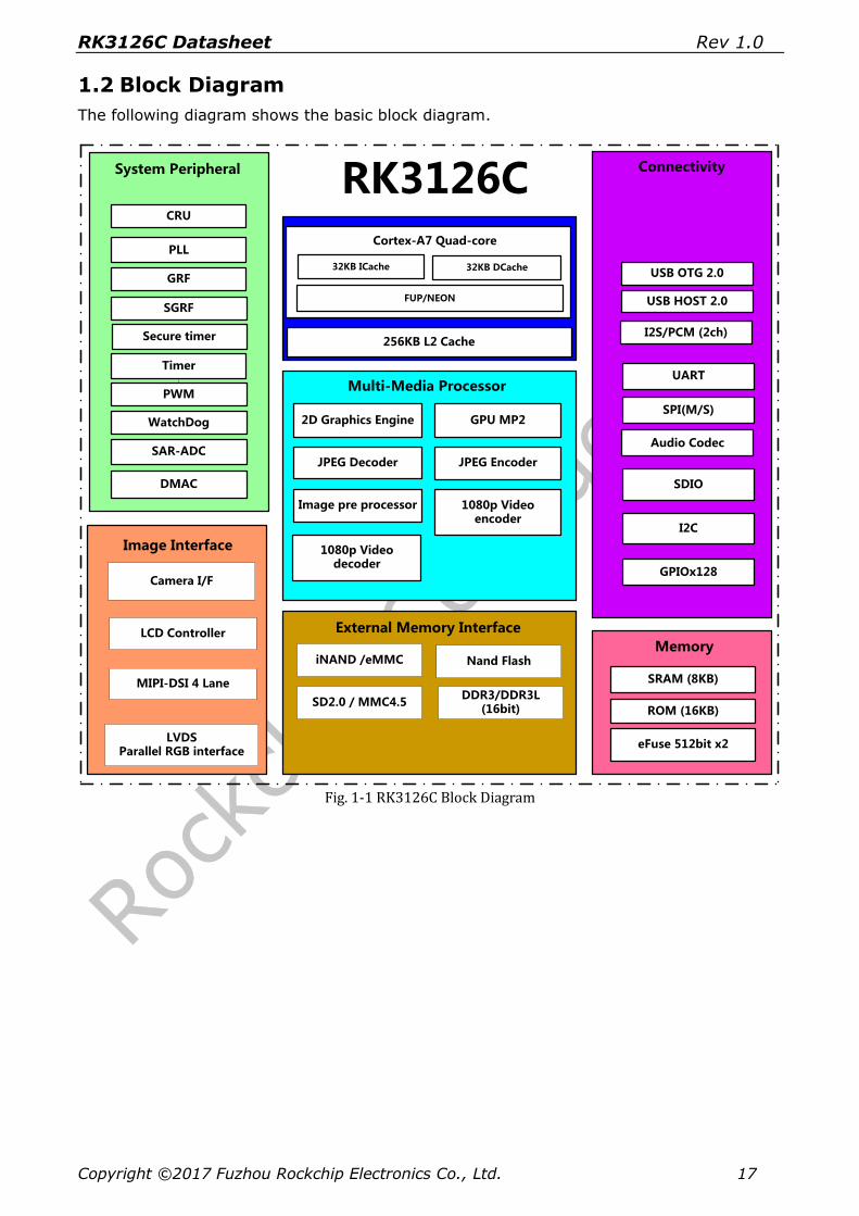
1.2 Block Diagram
The following diagram shows the basic block diagram.
RK3126C
256KB L2 Cache
LCD Controller
Camera I/F
Image Interface
2D Graphics Engine
1080p Video encoder
Image pre processor
GPU MP2
1080p Video decoder
JPEG EncoderJPEG Decoder
Nand Flash
External Memory Interface
DDR3/DDR3L(16bit)
SD2.0 / MMC4.5
iNAND /eMMC
USB OTG 2.0
SDIO
UART
I2C
SPI(M/S)
GPIOx128
USB HOST 2.0
Audio Codec
I2S/PCM (2ch)
Connectivity
DMAC
PWM
WatchDog
Timer
CRU
GRF
SAR-ADC
PLL
System Peripheral
SRAM (8KB)
ROM (16KB)
eFuse 512bit x2
Memory
Multi-Media Processor
32KB ICache
FUP/NEON
Cortex-A7 Quad-core
32KB DCache
LVDSParallel RGB interface
MIPI-DSI 4 Lane
SGRF
Secure timer
Fig. 1-1 RK3126C Block Diagram
RK3126C Datasheet Rev 1.0
Copyright ©2017 Fuzhou Rockchip Electronics Co., Ltd. 18
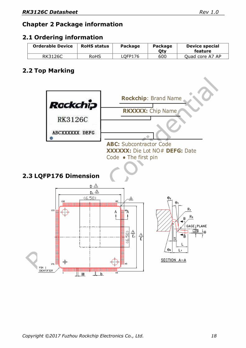
Chapter 2 Package information
2.1 Ordering information
Orderable Device RoHS status Package Package
Qty Device special
feature
RK3126C RoHS LQFP176 600 Quad core A7 AP
2.2 Top Marking
Rockchip: Brand Name
RKXXXX: Chip Name
ABC: Subcontractor CodeXXXXXX: Die Lot NO# DEFG: Date Code ● The first pin
2.3 LQFP176 Dimension

RK3126C Datasheet Rev 1.0
Copyright ©2017 Fuzhou Rockchip Electronics Co., Ltd. 19
Fig.2-1 RK3126C LQFP176 Package Top View
Fig.2-2 RK3126C LQFP176 Package Side View
Fig.2-3 RK3126C LQFP176 Package Dimension
RK3126C Datasheet Rev 1.0
Copyright ©2017 Fuzhou Rockchip Electronics Co., Ltd. 20
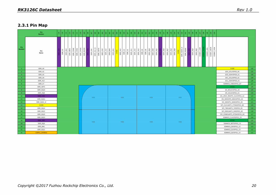
2.3.1 Pin Map
Pin
Number 176
175
174
173
172
171
170
169
168
167
166
165
164
163
162
161
160
159
158
157
156
155
154
153
152
151
150
149
148
147
146
145
144
143
142
141
140
139
138
137
136
135
134
133
Pin
Name
DD
R_V
DD
DD
R_A
3
DD
R_B
A2
DD
R_W
EN
DD
R_C
SN
0
DD
R_C
SN
1
DD
R_C
AS
N
DD
R_R
AS
N
DD
R_V
DD
DD
R_C
LK
DD
R_C
LK
_N
DD
R_O
DT
0
DD
R_C
KE
DD
R_A
10
DD
R_B
A0
DD
R_B
A1
CV
DD
DD
R_A
12
DD
R_A
4
DD
R_A
1
DD
R_A
11
DD
R_A
15
DD
R_A
14
DD
R_A
6
DD
R_A
8
DD
R_D
Q3
DD
R_D
M0
DD
R_D
Q1
DD
R_V
DD
DD
R_D
Q5
DD
R_D
Q7
DD
R_D
Q4
DD
R_D
Q6
CV
DD
DD
R_D
QS
0_N
DD
R_D
QS
0
DD
R_V
DD
DD
R_D
Q0
DD
R_D
Q2
CO
DE
C_A
OR
CO
DE
C_A
VD
D
CO
DE
C_A
OL
CO
DE
C_M
ICR
CO
DE
C_V
CM
1 DDR_A0 CVDD 132
2 DDR_A2 I2C0_SCL/GPIO0_A0 131
3 DDR_A5 I2C0_SDA/GPIO0_A1 130
4 DDR_A9 I2C1_SCL/GPIO0_A2 129
5 DDR_A13 I2C1_SDA/GPIO0_A3 128
6 DDR_A7 SDMMC0_CMD/GPIO1_B7 127
7 DDR_ODT1 VCCIO 126
8 DDR_DQ10 I2S_MCLK/GPIO1_A0 125
9 DDR_DQ8 I2S_SCLK/GPIO1_A1 124
10 DDR_VDD I2S_LRCK_RX/GPS_CLK/GPIO1_A2 123
11 DDR_DQS1 I2S_SDO/GPS_MAG/GPIO1_A4 122
12 DDR_DQS1_N I2S_SDI/GPS_SIGN/GPIO1_A5 121
13 CVDD SPI_CLK/UART1_CTSN/GPIO1_B0 120
14 DDR_DQ14 SPI_TXD/UART1_TX/GPIO1_B1 119
15 DDR_DQ12 SPI_RXD/UART1_RX/GPIO1_B2 118
16 DDR_DQ15 SPI_CSN0/UART1_RTSN/GPIO1_B3 117
17 DDR_DQ13 SDMMC0_CLKO/GPIO1_C0 116
18 DDR_VDD VCCIO 115
19 DDR_DQ9 SDMMC0_DET/GPIO1_C1 114
20 DDR_DM1 SDMMC0_D0/GPIO1_C2 113
21 DDR_DQ11 SDMMC0_D1/GPIO1_C3 112
22 C/DPLL_DVDD12 SDMMC0_D2/GPIO1_C4 111
VSS
VSS VSS VSS
VSS VSSVSS
Pin
Number
VSS
RK3126C Datasheet Rev 1.0
Copyright ©2017 Fuzhou Rockchip Electronics Co., Ltd. 21
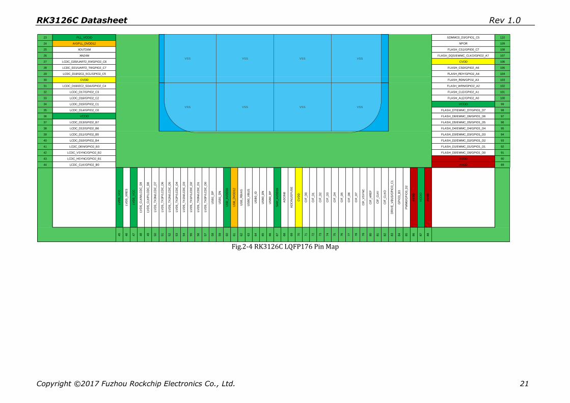
Fig.2-4 RK3126C LQFP176 Pin Map
23 PLL_VCCIO SDMMC0_D3/GPIO1_C5 110
24 A/GPLL_DVDD12 NPOR 109
25 XOUT24M FLASH_CS1/GPIO0_C7 108
26 XIN24M FLASH_DQS/EMMC_CLKO/GPIO2_A7 107
27 LCDC_D20/UART2_RX/GPIO2_C6 CVDD 106
28 LCDC_D21/UART2_TX/GPIO2_C7 FLASH_CS0/GPIO2_A6 105
29 LCDC_D19/I2C2_SCL/GPIO2_C5 FLASH_RDY/GPIO2_A4 104
30 CVDD FLASH_RDN/GPO2_A3 103
31 LCDC_D18/I2C2_SDA/GPIO2_C4 FLASH_WRN/GPIO2_A2 102
32 LCDC_D17/GPIO2_C3 FLASH_CLE/GPIO2_A1 101
33 LCDC_D16/GPIO2_C2 FLASH_ALE/GPIO2_A0 100
34 LCDC_D15/GPIO2_C1 VCCIO 99
35 LCDC_D14/GPIO2_C0 FLASH_D7/EMMC_D7/GPIO1_D7 98
36 VCCIO FLASH_D6/EMMC_D6/GPIO1_D6 97
37 LCDC_D13/GPIO2_B7 FLASH_D5/EMMC_D5/GPIO1_D5 96
38 LCDC_D12/GPIO2_B6 FLASH_D4/EMMC_D4/GPIO1_D4 95
39 LCDC_D11/GPIO2_B5 FLASH_D3/EMMC_D3/GPIO1_D3 94
40 LCDC_D10/GPIO2_B4 FLASH_D2/EMMC_D2/GPIO1_D2 93
41 LCDC_DEN/GPIO2_B3 FLASH_D1/EMMC_D1/GPIO1_D1 92
42 LCDC_VSYNC/GPIO2_B2 FLASH_D0/EMMC_D0/GPIO1_D0 91
43 LCDC_HSYNC/GPIO2_B1 AVDD 90
44 LCDC_CLK/GPIO2_B0 AVDD 89
LV
DS
_V
CC
LV
DS
_X
RE
S
LV
DS
_V
CC
LV
DS
_C
LK
N/L
CD
C_D
9
LV
DS
_C
LK
P/L
CD
C_D
8
LV
DS
_T
X3N
/LC
DC
_D
7
LV
DS
_T
X3P
/LC
DC
_D
6
LV
DS
_T
X2N
/LC
DC
_D
5
LV
DS
_T
X2P
/LC
DC
_D
4
LV
DS
_T
X1N
/LC
DC
_D
3
LV
DS
_T
X1P
/LC
DC
_D
2
LV
DS
_T
X0N
/LC
DC
_D
1
LV
DS
_T
X0P
/LC
DC
_D
0
US
B1_D
P
US
B1_D
N
US
B_A
VD
D33
US
B_D
VD
D12
US
B_R
BIA
S
US
B0_V
BU
S
US
B0_ID
US
B0_D
N
US
B0_D
P
SA
R_A
VD
D33
AD
CIN
0
AD
CIN
1/E
FU
SE
CV
DD
CIF
_D
0
CIF
_D
1
CIF
_D
2
CIF
_D
3
CIF
_D
4
CIF
_D
5
CIF
_D
6
CIF
_D
7
CIF
_V
SY
NC
CIF
_H
RE
F
CIF
_C
LK
I
CIF
_C
LK
O
DR
IVE
_V
BU
S/G
PIO
3_C
1
GP
IO3_B
3
PW
M0/G
PIO
0_D
2
AV
DD
VC
CIO
AV
DD
45
46
47
48
49
50
51
52
53
54
55
56
57
58
59
60
61
62
63
64
65
66
67
68
69
70
71
72
73
74
75
76
77
78
79
80
81
82
83
84
85
86
87
88
VSSVSS
VSS VSSVSSVSS
VSS VSS
RK3126C Datasheet Rev 1.0
Copyright ©2017 Fuzhou Rockchip Electronics Co., Ltd. 22
2.4 Pin Description
In this chapter, the pin description will be divided into two parts, one is all power/ground
descriptions in Table 1-1, include analog power/ground, another is all the function signals descriptions in Table 1-2, also include analog power/ground.
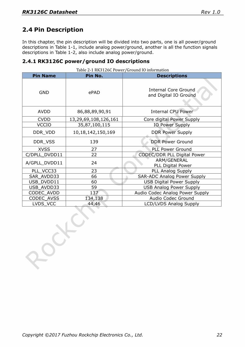
2.4.1 RK3126C power/ground IO descriptions
Table 2-1 RK3126C Power/Ground IO information
Pin Name Pin No. Descriptions
GND ePAD Internal Core Ground
and Digital IO Ground
AVDD 86,88,89,90,91 Internal CPU Power
CVDD 13,29,69,108,126,161 Core digital Power Supply
VCCIO 35,87,100,115 IO Power Supply
DDR_VDD 10,18,142,150,169 DDR Power Supply
DDR_VSS 139 DDR Power Ground
XVSS 27 PLL Power Ground
C/DPLL_DVDD11 22 CODEC/DDR PLL Digital Power
A/GPLL_DVDD11 24 ARM/GENERAL
PLL Digital Power
PLL_VCC33 23 PLL Analog Supply
SAR_AVDD33 66 SAR-ADC Analog Power Supply
USB_DVDD11 60 USB Digital Power Supply
USB_AVDD33 59 USB Analog Power Supply
CODEC_AVDD 137 Audio Codec Analog Power Supply
CODEC_AVSS 134,138 Audio Codec Ground
LVDS_VCC 44,46 LCD/LVDS Analog Supply
RK3126C Datasheet Rev 1.0
Copyright ©2017 Fuzhou Rockchip Electronics Co., Ltd. 23
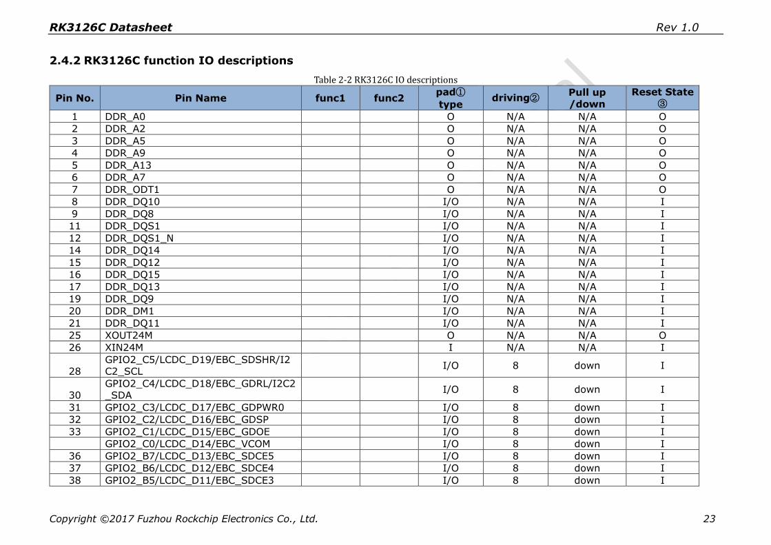
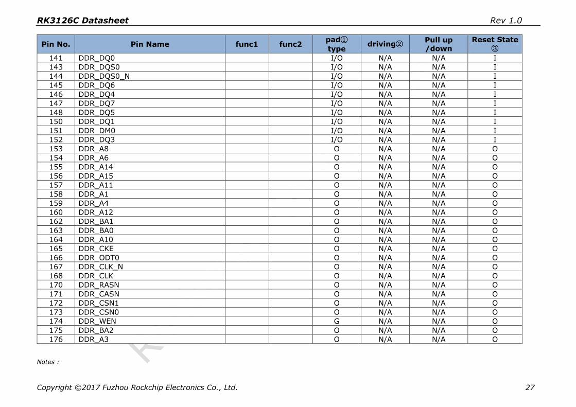
2.4.2 RK3126C function IO descriptions
Table 2-2 RK3126C IO descriptions
Pin No. Pin Name func1 func2 pad①
type driving②
Pull up
/down
Reset State③
1 DDR_A0 O N/A N/A O
2 DDR_A2 O N/A N/A O
3 DDR_A5 O N/A N/A O
4 DDR_A9 O N/A N/A O
5 DDR_A13 O N/A N/A O
6 DDR_A7 O N/A N/A O
7 DDR_ODT1 O N/A N/A O
8 DDR_DQ10 I/O N/A N/A I
9 DDR_DQ8 I/O N/A N/A I
11 DDR_DQS1 I/O N/A N/A I
12 DDR_DQS1_N I/O N/A N/A I
14 DDR_DQ14 I/O N/A N/A I
15 DDR_DQ12 I/O N/A N/A I
16 DDR_DQ15 I/O N/A N/A I
17 DDR_DQ13 I/O N/A N/A I
19 DDR_DQ9 I/O N/A N/A I
20 DDR_DM1 I/O N/A N/A I
21 DDR_DQ11 I/O N/A N/A I
25 XOUT24M O N/A N/A O
26 XIN24M I N/A N/A I
28 GPIO2_C5/LCDC_D19/EBC_SDSHR/I2C2_SCL
I/O 8 down I
30 GPIO2_C4/LCDC_D18/EBC_GDRL/I2C2_SDA
I/O 8 down I
31 GPIO2_C3/LCDC_D17/EBC_GDPWR0 I/O 8 down I
32 GPIO2_C2/LCDC_D16/EBC_GDSP I/O 8 down I
33 GPIO2_C1/LCDC_D15/EBC_GDOE I/O 8 down I
GPIO2_C0/LCDC_D14/EBC_VCOM I/O 8 down I
36 GPIO2_B7/LCDC_D13/EBC_SDCE5 I/O 8 down I
37 GPIO2_B6/LCDC_D12/EBC_SDCE4 I/O 8 down I
38 GPIO2_B5/LCDC_D11/EBC_SDCE3 I/O 8 down I

RK3126C Datasheet Rev 1.0
Copyright ©2017 Fuzhou Rockchip Electronics Co., Ltd. 24
Pin No. Pin Name func1 func2 pad①
type driving②
Pull up /down
Reset State③
39 GPIO2_B4/LCDC_D10/EBC_SDCE2 I/O 8 down I
40 GPIO2_B3/LCD_DEN/EBC_GDCLK I/O 8 down I
41 GPIO2_B2/LCD_VSYNC/EBC_SDOE I/O 8 down I
42 GPIO2_B1/LCDC_HSYNC/EBC_SDLE I/O 8 down I
43 GPIO2_B0/LCDC_CLK/EBC_SDCLK I/O 12 down I
45 LVDS_EXTR A N/A N/A N/A
47 LCDC_D9/LVDS_CLKN/EBC_SDCE1/MIPI_CLKN
A N/A N/A N/A
48
LCDC_D8/LVDS_CLKP/EBC_SDCE0/MI
PI_CLKP A N/A N/A N/A
49
LCDC_D7/LVDS_TX3N/EBC_SDDO7/MI
PI_D3N A N/A N/A N/A
50
LCDC_D6/LVDS_TX3P/EBC_SDDO6/MI
PI_D3P A N/A N/A N/A
51 LCDC_D5/LVDS_TX2N/EBC_SDDO5/MIPI_D2N
A N/A N/A N/A
52 LCDC_D4/LVDS_TX2P/EBC_SDDO4/MIPI_D2P
A N/A N/A N/A
53 LCDC_D3/LVDS_TX1N/EBC_SDDO3/MIPI_D1N
A N/A N/A N/A
54 LCDC_D2/LVDS_TX1P/EBC_SDDO2/MIPI_D1P
A N/A N/A N/A
55
LCDC_D1/LVDS_TX0N/EBC_SDDO1/MI
PI_D0N A N/A N/A N/A
56
LCDC_D0/LVDS_TX0P/EBC_SDDO0/MI
PI_D0P A N/A N/A N/A
57 HOST_DP A N/A N/A N/A
58 HOST_DM A N/A N/A N/A
61 USB_EXTR A N/A N/A N/A
62 OTG_VBUS A N/A N/A N/A
63 OTG_ID A N/A N/A N/A
64 OTG_DM A N/A N/A N/A
65 OTG_DP A N/A N/A N/A
67 ADCIN0 A N/A N/A N/A
68 ADCIN3/EFUSE A N/A N/A N/A

RK3126C Datasheet Rev 1.0
Copyright ©2017 Fuzhou Rockchip Electronics Co., Ltd. 25
Pin No. Pin Name func1 func2 pad①
type driving②
Pull up /down
Reset State③
70 CIF_D0/TS_D0 I N/A down I
71 CIF_D1/TS_D1 I N/A down I
72 CIF_D2/TS_D2 I N/A down I
73 CIF_D3/TS_D3 I N/A down I
74 CIF_D4/TS_D4 I N/A down I
75 CIF_D5/TS_D5 I N/A down I
76 CIF_D6/TS_D6 I N/A down I
77 CIF_D7/TS_D7 I N/A down I
78 CIF_VSYNC/TS_SYNC I N/A down I
79 CIF_HREF/TS_FAIL I N/A down I
80 CIF_CLKI/TS_VALID I N/A down I
81 CIF_CLKO/TS_CLKO I/O 4 down I
82 GPIO3_C1/DRIVE_VBUS/PMIC_SLEEP I/O 4 down I
83 GPIO3_B3/CIF_PDN I/O 4 up I
84 GPIO0_D2/PWM0 I/O 4 down I
85 GPIO0_D3/PWM1 I/O 4 down I
92 GPIO1_C6/FLASH_CS2/EMMC_CMD I/O 4 up I
93
GPIO1_D0/FLASH_D0/EMMC_D0/SFC_
SIO0 I/O 8 up I
94 GPIO1_D1/FLASH_D1/EMMC_D1/SFC_SIO1
I/O 8 up I
95 GPIO1_D2/FLASH_D2/EMMC_D2/SFC_SIO2
I/O 8 up I
96 GPIO1_D3/FLASH_D3/EMMC_D3/SFC_SIO3
I/O 8 up I
97 GPIO1_D4/FLASH_D4/EMMC_D4/SPI_RXD
I/O 8 up I
98
GPIO1_D5/FLASH_D5/EMMC_D5/SPI_
TXD I/O 8 up I
99
GPIO1_D6/FLASH_D6/EMMC_D6/SPI_
CSN0 I/O 8 up I
100 GPIO1_D7/FLASH_D7/EMMC_D7/SPI_CSN1
I/O 8 up I
102 GPIO2_A0/FLASH_ALE/SPI_CLK I/O 8 down I
103 GPIO2_A1/FLASH_CLE I/O 8 down I

RK3126C Datasheet Rev 1.0
Copyright ©2017 Fuzhou Rockchip Electronics Co., Ltd. 26
Pin No. Pin Name func1 func2 pad①
type driving②
Pull up /down
Reset State③
104 GPIO2_A2/FLASH_WRN/SFC_CSN0 I/O 8 up I
105 GPIO2_A3/FLASH_RDN/SFC_CSN1 I/O 8 up I
106 GPIO2_A4/FLASH_RDY/EMMC_CMD/SFC_CLK
I/O 8 up I
107 GPIO2_A6/FLASH_CS0 I/O 8 up I
109 GPIO2_A7/FLASH_DQS/EMMC_CLKO I/O 8 up I
110 NPOR I N/A down I
111 GPIO1_C5/SDMMC0_D3/JTAG_TMS I/O 4 up I
112 GPIO1_C4/SDMMC0_D2/JTAG_TCK I/O 4 up I
113 GPIO1_C3/SDMMC0_D1/UART2_RX I/O 4 up I
114 GPIO1_C2/SDMMC0_D0/UART2_TX I/O 4 up I
116 GPIO1_C0/SDMMC0_CLKO I/O 4 down I
117 GPIO1_B3/UART1_RTSN/SPI_CSN0 I/O 4 up I
118 GPIO1_B2/UART1_RX/SPI_RXD I/O 4 up I
119 GPIO1_B1/UART1_TX/SPI_TXD I/O 4 up I
120 GPIO1_B0/UART1_CTSN/SPI_CLK I/O 4 up I
121 GPIO1_A5/I2S_SDI/SDMMC1_D3 I/O 4 down I
122 GPIO1_A4/I2S_SDO/SDMMC1_D2 I/O 4 down I
123
GPIO1_A2/I2S_LRCK_RX/SDMMC1_D1
for Version A I/O 4 up I
123 GPIO1_A2/I2S_LRCK_RX/SDMMC1_D1 for Version B
I/O 4 down I
124 GPIO1_A1/I2S_SCLK/SDMMC1_D0 I/O 4 down I
125
GPIO1_A0/I2S_MCLK/SDMMC1_CLKO/
XIN_32K I/O 4 down I
127 GPIO1_B7/SDMMC0_CMD I/O 4 up I
128 GPIO0_A3/I2C1_SDA/SDMMC1_CMD I/O 4 up I
129 GPIO0_A2/I2C1_SCL I/O 4 up I
130 GPIO0_A1/I2C0_SDA I/O 4 up I
131 GPIO0_A0/I2C0_SCL I/O 4 up I
132 CODEC_VCM A N/A N/A N/A
133 CODEC_MIC A N/A N/A N/A
135 CODEC_AOL A N/A N/A N/A
137 CODEC_AOR A N/A N/A N/A
140 DDR_DQ2 I/O N/A N/A I
RK3126C Datasheet Rev 1.0
Copyright ©2017 Fuzhou Rockchip Electronics Co., Ltd. 27
Pin No. Pin Name func1 func2 pad①
type driving②
Pull up /down
Reset State③
141 DDR_DQ0 I/O N/A N/A I
143 DDR_DQS0 I/O N/A N/A I
144 DDR_DQS0_N I/O N/A N/A I
145 DDR_DQ6 I/O N/A N/A I
146 DDR_DQ4 I/O N/A N/A I
147 DDR_DQ7 I/O N/A N/A I
148 DDR_DQ5 I/O N/A N/A I
150 DDR_DQ1 I/O N/A N/A I
151 DDR_DM0 I/O N/A N/A I
152 DDR_DQ3 I/O N/A N/A I
153 DDR_A8 O N/A N/A O
154 DDR_A6 O N/A N/A O
155 DDR_A14 O N/A N/A O
156 DDR_A15 O N/A N/A O
157 DDR_A11 O N/A N/A O
158 DDR_A1 O N/A N/A O
159 DDR_A4 O N/A N/A O
160 DDR_A12 O N/A N/A O
162 DDR_BA1 O N/A N/A O
163 DDR_BA0 O N/A N/A O
164 DDR_A10 O N/A N/A O
165 DDR_CKE O N/A N/A O
166 DDR_ODT0 O N/A N/A O
167 DDR_CLK_N O N/A N/A O
168 DDR_CLK O N/A N/A O
170 DDR_RASN O N/A N/A O
171 DDR_CASN O N/A N/A O
172 DDR_CSN1 O N/A N/A O
173 DDR_CSN0 O N/A N/A O
174 DDR_WEN G N/A N/A O
175 DDR_BA2 O N/A N/A O
176 DDR_A3 O N/A N/A O
Notes :
RK3126C Datasheet Rev 1.0
Copyright ©2017 Fuzhou Rockchip Electronics Co., Ltd. 28
① : Pad types : I = input , O = output , I/O = input/output (bidirectional) ,
AP = Analog Power , AG = Analog Ground, DP = Digital Power , DG = Digital Ground, A = Analog ②:Output Drive Unit is mA , only Digital IO have drive value
③:Reset state : I = input without any pull resistor ,O = output without any pull resistor ,
④:It is die location. For examples, “Left side” means that all the related IOs are always in left side of die
⑤:Power supply means that all the related IOs is in these IO power domain. If multiple powers is included, they are connected together in one IO power ring

RK3126C Datasheet Rev1.0
Copyright ©2017 Fuzhou Rockchip Electronics Co., Ltd. 29
2.4.3 IO pin name descriptions
This sub-chapter will focus on the detailed function description of every pins based on different interface.
Table 2-3 RK3126C IO function description list
Interface Pin Name Direction Description
Misc
XIN24M I Clock input of 24MHz crystal
XOUT24M O Clock output of 24MHz crystal
NPOR I Power on reset for chip
Interface Pin Name Direction Description
Debug
TCK I JTAG interface clock input/SWD interface clock input
TMS I/O JTAG interface TMS input/SWD interface data out
Interface Pin Name Direction Description
SD/MMC Host
Controller
sdmmc_clkout O sdmmc card clock.
sdmmc_cmd I/O sdmmc card command output and reponse input.
sdmmc_datai (i=0~3)
I/O sdmmc card data input and output.
Interface Pin Name Direction Description
SDIO Host Controller
sdio_clkout O sdio card clock.
sdio_cmd I/O sdio card command output and reponse input.
sdio_datai (i=0~3)
I/O sdio card data input and output.
Interface Pin Name Direction Description
eMMC Interface
emmc_clkout O emmc card clock.
emmc_cmd I/O emmc card command output and reponse input.
emmc_datai (i=0~7)
I/O emmc card data input and output.
emmc_pwr_en O emmc card power-enable control signal
emmc_rstn_out O emmc card reset signal
Interface Pin Name Direction Description
DMC
CLK O Active-high clock signal to the memory
device.
CLK_N O Active-low clock signal to the memory device.
CKE O Active-high clock enable signal to the memory device
CSNi (i=0,1)
O Active-low chip select signal to the memory device. AThere are two chip select.
RASN O Active-low row address strobe to the memory device.
RK3126C Datasheet Rev1.0
Copyright ©2017 Fuzhou Rockchip Electronics Co., Ltd. 30
Interface Pin Name Direction Description
CASN O Active-low column address strobe to the memory device.
WEN O Active-low write enable strobe to the memory device.
BAi (i=0,1,2)
O Bank address signal to the memory device.
Ai (i=0~15)
O Address signal to the memory device.
DQi
(i=0~15) I/O
Bidirectional data line to the memory
device.
DQS0
DQS1 I/O
Active-high bidirectional data strobes to
the memory device.
DQS0_N
DQS1_N I/O
Active-low bidirectional data strobes to
the memory device.
DMi (i=0,1)
O Active-low data mask signal to the memory device.
ODTi (i=0,1)
O On-Die Termination output signal for two chip select.
Interface Pin Name Direction Description
NandC
flash_wp O Flash write-protected signal
flash_ale O Flash address latch enable signal
flash_cle O Flash command latch enable signal
flash_wrn O Flash write enable and clock signal
flash_rdn O Flash read enable and write/read signal
flash_datai (i=0~7)
I/O 8bits of flash data inputs/outputs signal
flash_dqs I/O Flash data strobe signal
flash_rdy I Flash ready/busy signal
flash_csni
(i=0,2) O
Flash chip enable signal for chip i,
i=0,2
Interface Pin Name Direction Description
SPI Controller
spi_clk I/O spi serial clock
spi_csni (i =0,1)
I/O spi chip select signal,low active
spi_txd O spi serial data output
spi_rxd I spi serial data input
RK3126C Datasheet Rev1.0
Copyright ©2017 Fuzhou Rockchip Electronics Co., Ltd. 31
Interface Pin Name Direction Description
LCDC
lcdc_dclk O LCDC RGB interface display clock out, MCU i80 interface RS signal
lcdc_vsync O LCDC RGB interface vertival sync pulse,
MCU i80 interface CSN signal
lcdc_hsync O LCDC RGB interface horizontial sync
pulse, MCU i80 interface WEN signal
lcdc_den O LCDC RGB interface data enable, MCU i80 interface REN signal
lcdc_data i (i=0~19) I/O LCDC data output/input
Interface Pin Name Direction Description
Camera IF
cif_clkin I Camera interface input pixel clock
cif_clkout O Camera interface output work clock
cif_vsync I Camera interface vertical sync signal
cif_href I Camera interface horizontial sync signal
cif_datai (i=0~7) I Camera interface 8-bit input pixel data
Interface Pin Name Direction Description
PWM pwm1 O Pulse Width Modulation output
pwm0 O Pulse Width Modulation output
Interface Pin Name Direction Description
I2C
i2c0_sda I/O I2C0 data
i2c0_scl I/O I2C0 clock
i2c1_sda I/O I2C1 data
i2c1_scl I/O I2C1 clock
i2c2_sda I/O I2C2 data
i2c2_scl I/O I2C2 clock
Interface Pin Name Direction Description
UART
uart1_sin I UART1 searial data input
uart1_sout O UART1 searial data output
uart1_cts_n O UART1 clear to send
uart1_rts_n I UART1 request to send
uart2_sin I UART2 searial data input
uart2_sout O UART2 searial data output
Interface Pin Name Direction Description
USB OTG2.0
/HOST 2.0
OTG_DP I/O USB OTG 2.0 Data signal DP
OTG_DM I/O USB OTG 2.0 Data signal DM
OTG_VBUS N/A USB OTG 2.0 5V power supply pin
OTG_ID I USB OTG 2.0 ID indicator
HOST_DP I/O USB HOST 2.0 Data signal DP
HOST_DM I/O USB HOST 2.0 Data signal DM
USB_EXTR N/A 133 Ohm Reference external resistance
Interface Pin Name Direction Description

RK3126C Datasheet Rev1.0
Copyright ©2017 Fuzhou Rockchip Electronics Co., Ltd. 32
Audio Codec
MIC I Microphone input
VCM I Decoupling for voltage reference
AOL O Left channel DAC driver amplifier output
AOR O Right channel DAC driver amplifier
output
Interface Pin Name Direction Description
LVDS
lvds/mipi_extr I Connected to external 12Komh through bonding pad
lvds_txp_n O Transmit serial data out(Positive),
n=1~4
lvds_txn_n O Transmit serial data out(Negative),
n=1~4
lvds_clkp O Output clock
lvds_clkn O Output clock(Negative)
Interface Pin Name Direction Description
MIPI
lvds/mipi_extr I Connected to external 12Komh through
bonding pad
mipiDiP
(i=0~3) O
Transmit serial data out(Positive),
i=0~3
mipiDiN (i=0~3)
O Transmit serial data out(Negative), i=0~3
mipi_clkp O Output clock(Positive)
mipi_clkn O Output clock(Negative)
Interface Pin Name Direction Description
SAR-ADC Saradc_ain i (i =0,2)
N/A SAR-ADC input signal for 3 channel
Interface Pin Name Direction Description
eFuse efuse_vp N/A eFuse program and sense power
2.4.4 RK3126C IO Type
The following list shows IO type except DDR IO and all of Power/Ground IO .
Table 2-4 RK3126C IO Type List
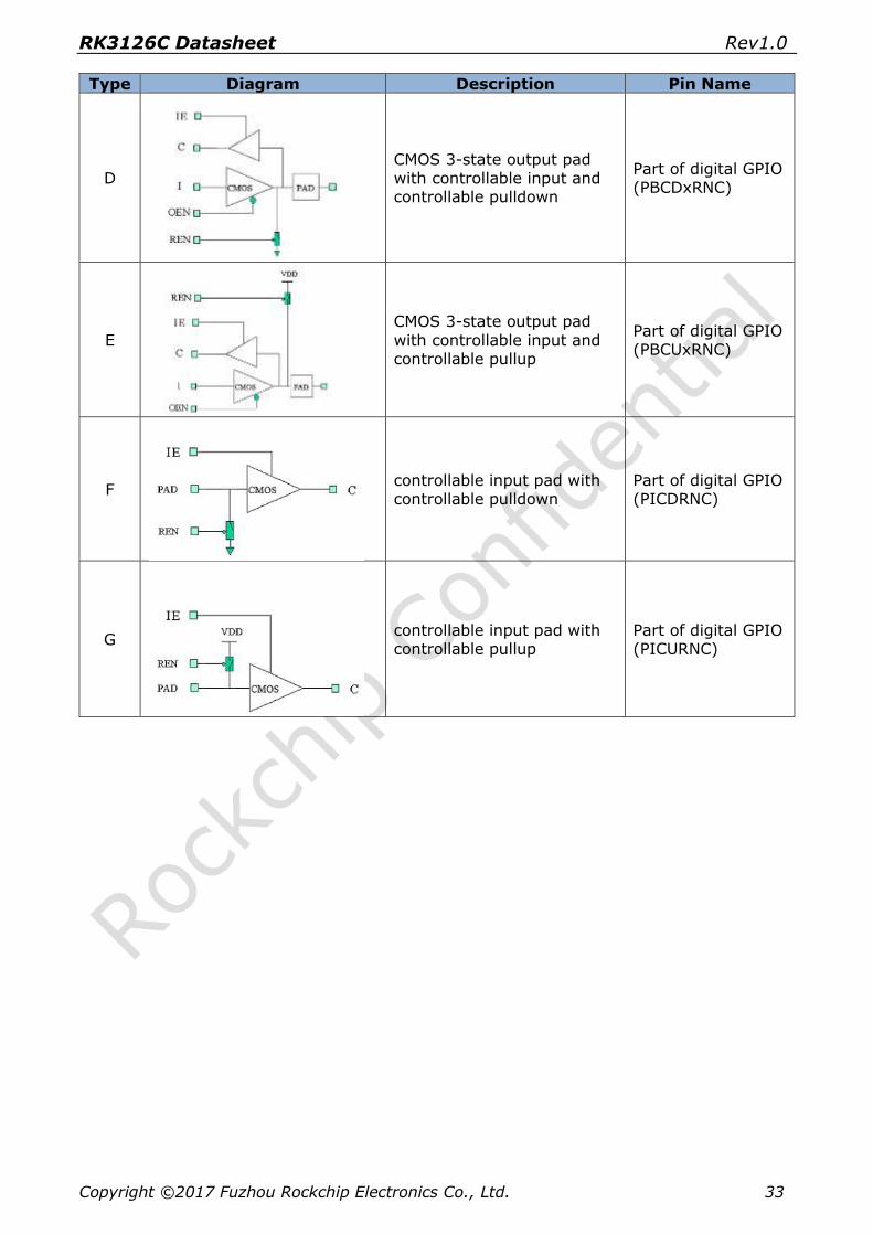
Type Diagram Description Pin Name
A
Analog IO Cell with IO voltage
EFUSE_VP
B
Dedicated Power supply to
Internal Macro with IO voltage
SARADC_AIN[2:0]
C
Crystal Oscillator with
internal register XIN24M/XOUT24M
RK3126C Datasheet Rev1.0
Copyright ©2017 Fuzhou Rockchip Electronics Co., Ltd. 33
Type Diagram Description Pin Name
D
CMOS 3-state output pad with controllable input and controllable pulldown
Part of digital GPIO (PBCDxRNC)
E
CMOS 3-state output pad
with controllable input and controllable pullup
Part of digital GPIO (PBCUxRNC)
F
controllable input pad with controllable pulldown
Part of digital GPIO (PICDRNC)
G
controllable input pad with controllable pullup
Part of digital GPIO (PICURNC)
RK3126C Datasheet Rev1.0
Copyright ©2017 Fuzhou Rockchip Electronics Co., Ltd. 34
Chapter 3 Electrical Specification
3.1 Absolute Maximum Ratings
Table 3-1 RK3126C absolute maximum ratings
Paramerters Related Power Group Max Unit
DC supply voltage for Internal digital logic AVDD,CVDD, TBD V
DC supply voltage for Internal digital logic USB_DVDD11,LVDS_DVDD11 1.2
1 V
DC supply voltage for Digital GPIO (except for SAR-ADC, PLL, USB, DDR IO)
VCCIO 3.63
V
DC supply voltage for DDR IO VCC_DDR 1.95
V
DC supply voltage for Analog part of SAR-
ADC and PLL SAR_AVDD33,PLL_VCCIO
3.6
3 V
DC supply voltage for Analog part of PLL A/GPLL_DVDD11,C/DPLL_DVDD11
1.21
V
DC supply voltage for Analog part of USB OTG/Host2.0
USB_AVDD33 3.63
V
DC supply voltage for Analog part of Acodec CODEC_AVDD 3.6
3 V
DC supply voltage for Analog part of LVDS LVDS_VCC 3.6
3 V
Analog Input voltage for SAR-ADC 2.75
V
Analog Input voltage for DP/DM/VBUS of USB OTG/Host2.0
5.25
V
Digital input voltage for input buffer of GPIO 3.63
V
Digital output voltage for output buffer of GPIO
3.63
V
Storage Temperature Tstg 125 C
Max Conjunction Temperature Tj 125 ℃
Absolute maximum ratings specify the values beyond which the device may be damaged
permanently. Long-term exposure to absolute maximum ratings conditions may affect device reliability.
3.2 Recommended Operating Conditions
Table 3-2 RK3126C recommended operating conditions
Parameters Symbol Min Typ Max Units
Internal digital Core
Power AVDD 0.9 TBD TBD V
Internal digital logic Power
CVDD,USB_DVDD11,LVDS_DVDD11 0.9 1.1 1.21 V
Digital GPIO Power VCCIO 2.97 3.3 3.63 V
DDR IO (DDR3 mode) Power
VCC_DDR 1.425 1.5 1.575 V

RK3126C Datasheet Rev1.0
Copyright ©2017 Fuzhou Rockchip Electronics Co., Ltd. 35
Parameters Symbol Min Typ Max Units
DDR IO (DDR3L
mode) Power VCC_DDR 1.28 1.35 1.45 V
PLL Analog Power PLL_VCCIO 2.97 3.3 3.63 V
PLL Analog Power A/GPLL_DVDD11,C/DPLL_DVDD11 0.99 1.1 1.21 V
SAR-ADC Analog
Power SAR_AVDD33 2.97 3.3 3.63 V
USB OTG/Host2.0
Analog Power(3.3V) USB_AVDD33 2.97 3.3 3.63 V
USB OTG/Host2.0 external resistor
EXTR 122 135 147 Ohm
Acodec Analog Power CODEC_AVDD 2.97 3.3 3.63 V
EFUSE programming voltage
2.25 2.5 2.75 V
PLL input clock
frequency 24 MHz
Ambient Operating
Temperature ○2 Ta 0 25 80 ℃
Notes : ①:Symbol name is same as the pin name in the io descriptions
○2 with the reference software setup, the reference software will limit the chipset temperature about
80℃
3.3 DC Characteristics
Table 3-3 RK3126C DC Characteristics
Parameters Symbol Min Typ Max Units
Digital GPIO
Input Low Voltage Vil -0.3 0 0.8 V
Input High Voltage Vih 2 3.3 3.6 V
Output Low Voltage Vol 0 0.4 V
Output High Voltage
Voh 2.4 3.3 V
Threshold Point Vt 1.21 1.42 1.64 V
Schmitt trig Low to High threshold
point
Vt+ 1.36 1.6 1.86 V
Schmitt trig High to
Low threshold point Vt- 0.93 1.09 1.3 V
Pullup Resistor Rpu 33 41 62 Kohm
Pulldown Resistor Rpd 33 42 68 Kohm
DDR IO (Data)
DC Input High
Voltage Vih(DC) VREF + 0.1
VDDQ+
0.4 V
AC Input High
Voltage Vih(AC)
VREF +
0.15
VDDQ+
0.4 V
DC Input Low Voltage
Vil(DC) -0.4 VREF - 0.1 V
AC Input Low Voltage
Vil(AC) -0.4 VREF +
0.15 V
Differential input logic high
Vihdiff +0.2 VDDQ +
0.4 V
Differential input logic low
Vildiff -0.4 -0.2 V
Output High
Voltage Voh 0.9 * VDDQ VDDQ V
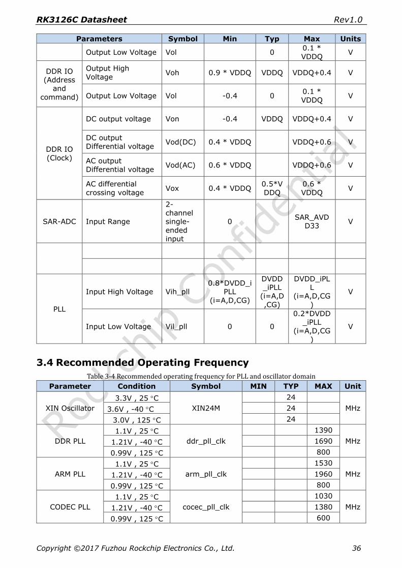
RK3126C Datasheet Rev1.0
Copyright ©2017 Fuzhou Rockchip Electronics Co., Ltd. 36
Parameters Symbol Min Typ Max Units
Output Low Voltage Vol 0 0.1 *
VDDQ V
DDR IO (Address
and
command)
Output High
Voltage Voh 0.9 * VDDQ VDDQ VDDQ+0.4 V
Output Low Voltage Vol -0.4 0 0.1 * VDDQ
V
DDR IO
(Clock)
DC output voltage Von -0.4 VDDQ VDDQ+0.4 V
DC output Differential voltage
Vod(DC) 0.4 * VDDQ VDDQ+0.6 V
AC output Differential voltage
Vod(AC) 0.6 * VDDQ VDDQ+0.6 V
AC differential
crossing voltage Vox 0.4 * VDDQ
0.5*V
DDQ
0.6 *
VDDQ V
SAR-ADC Input Range
2-channel single-
ended input
0 SAR_AVD
D33 V
PLL
Input High Voltage Vih_pll 0.8*DVDD_i
PLL
(i=A,D,CG)
DVDD_iPLL
(i=A,D
,CG)
DVDD_iPLL
(i=A,D,CG
)
V
Input Low Voltage Vil_pll 0 0
0.2*DVDD
_iPLL (i=A,D,CG
)
V
3.4 Recommended Operating Frequency
Table 3-4 Recommended operating frequency for PLL and oscillator domain
Parameter Condition Symbol MIN TYP MAX Unit
XIN Oscillator
3.3V , 25 C
XIN24M
24
MHz 3.6V , -40 C 24
3.0V , 125 C 24
DDR PLL
1.1V , 25 C
ddr_pll_clk
1390
MHz 1.21V , -40 C 1690
0.99V , 125 C 800
ARM PLL
1.1V , 25 C
arm_pll_clk
1530
MHz 1.21V , -40 C 1960
0.99V , 125 C 800
CODEC PLL
1.1V , 25 C
cocec_pll_clk
1030
MHz 1.21V , -40 C 1380
0.99V , 125 C 600
RK3126C Datasheet Rev1.0
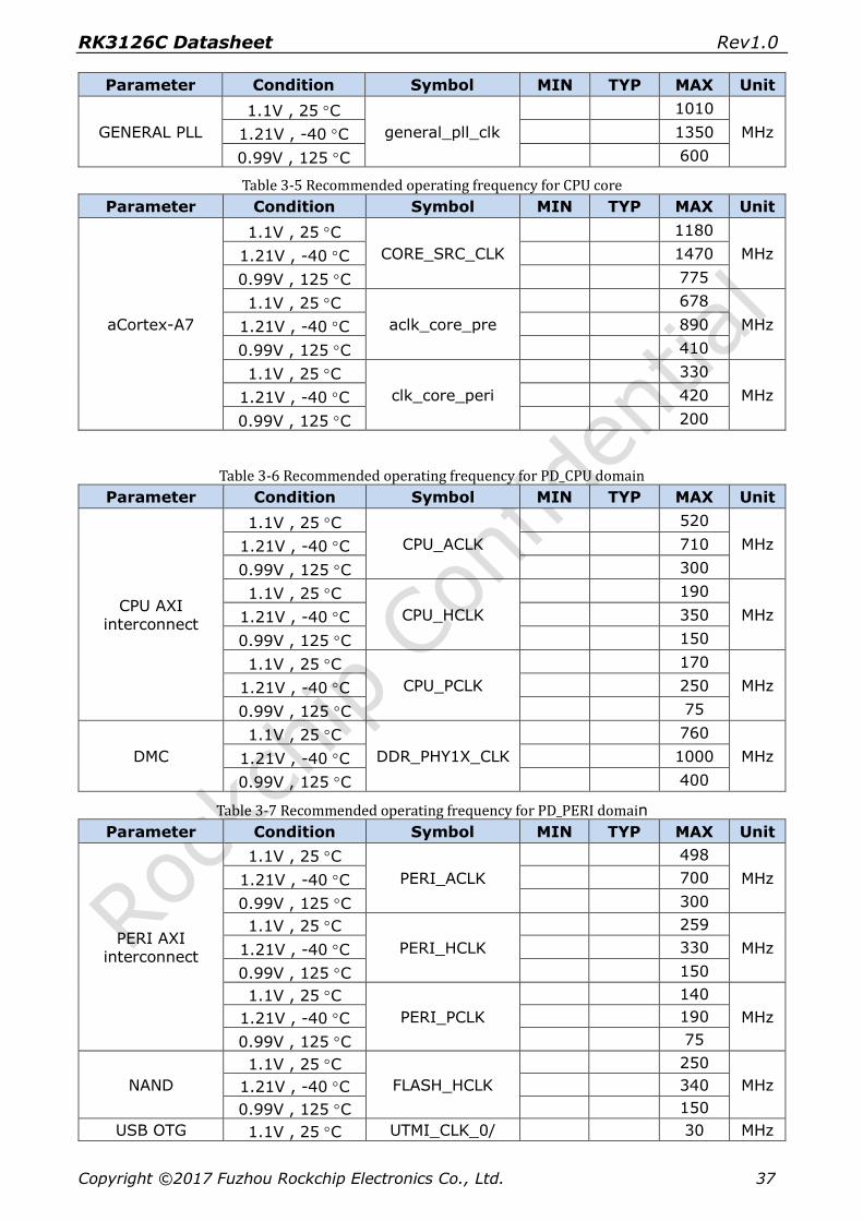
Copyright ©2017 Fuzhou Rockchip Electronics Co., Ltd. 37
Parameter Condition Symbol MIN TYP MAX Unit
GENERAL PLL
1.1V , 25 C
general_pll_clk
1010
MHz 1.21V , -40 C 1350
0.99V , 125 C 600
Table 3-5 Recommended operating frequency for CPU core
Parameter Condition Symbol MIN TYP MAX Unit
aCortex-A7
1.1V , 25 C
CORE_SRC_CLK
1180
MHz 1.21V , -40 C 1470
0.99V , 125 C 775
1.1V , 25 C
aclk_core_pre
678
MHz 1.21V , -40 C 890
0.99V , 125 C 410
1.1V , 25 C
clk_core_peri
330
MHz 1.21V , -40 C 420
0.99V , 125 C 200
Table 3-6 Recommended operating frequency for PD_CPU domain
Parameter Condition Symbol MIN TYP MAX Unit
CPU AXI interconnect
1.1V , 25 C
CPU_ACLK
520
MHz 1.21V , -40 C 710
0.99V , 125 C 300
1.1V , 25 C
CPU_HCLK
190
MHz 1.21V , -40 C 350
0.99V , 125 C 150
1.1V , 25 C
CPU_PCLK
170
MHz 1.21V , -40 C 250
0.99V , 125 C 75
DMC
1.1V , 25 C
DDR_PHY1X_CLK
760
MHz 1.21V , -40 C 1000
0.99V , 125 C 400
Table 3-7 Recommended operating frequency for PD_PERI domain
Parameter Condition Symbol MIN TYP MAX Unit
PERI AXI interconnect
1.1V , 25 C
PERI_ACLK
498
MHz 1.21V , -40 C 700
0.99V , 125 C 300
1.1V , 25 C
PERI_HCLK
259
MHz 1.21V , -40 C 330
0.99V , 125 C 150
1.1V , 25 C
PERI_PCLK
140
MHz 1.21V , -40 C 190
0.99V , 125 C 75
NAND
1.1V , 25 C
FLASH_HCLK
250
MHz 1.21V , -40 C 340
0.99V , 125 C 150
USB OTG 1.1V , 25 C UTMI_CLK_0/ 30 MHz

RK3126C Datasheet Rev1.0
Copyright ©2017 Fuzhou Rockchip Electronics Co., Ltd. 38
Parameter Condition Symbol MIN TYP MAX Unit
1.21V , -40 C UTMI_CLK_1 30
0.99V , 125 C 30
UART1
1.1V , 25 C
UART1_CLK
50
MHz 1.21V , -40 C 50
0.99V , 125 C 50
SDMMC/SDIO
1.1V , 25 C MMC0_CLK/ SDIO_CLK
100
MHz 1.21V , -40 C 100
0.99V , 125 C 100
EMMC
1.1V , 25 C
EMMC_CLK
100
MHz 1.21V , -40 C 100
0.99V , 125 C 100
I2S
1.1V , 25 C
I2S_CLK
50
MHz 1.21V , -40 C 50
0.99V , 125 C 50
SPI0
1.1V , 25 C
SPI0_CLK
50
MHz 1.21V , -40 C 50
0.99V , 125 C 50
SAR-ADC
1.1V , 25 C
SARADC_CLK
12
MHz 1.21V , -40 C 12
0.99V , 125 C 12
Timer0/1
1.1V , 25 C TIMER0_CLK/
TIMER1_CLK
24
MHz 1.21V , -40 C 24
0.99V , 125 C 24
1.1V , 25 C TIMER0_PCLK/ TIMER1_PCLK
140
MHz 1.21V , -40 C 190
0.99V , 125 C 75
Table 3-8 Recommended operating frequency for PD_VIO domain
Parameter Condition Symbol MIN TYP MAX Unit
Display AXI interconnection
1.1V , 25 C
DISP_ACLK
530
MHz 1.21V , -40 C 720
0.99V , 125 C 300
1.1V , 25 C
DISP_HCLK
370
MHz 1.21V , -40 C 500
0.99V , 125 C 200
LCDC
1.1V , 25 C
LCDC_DCLK
179
MHz 1.21V , -40 C 190
0.99V , 125 C 160
1.1V , 25 C
LCDC1_DCLK
230
MHz 1.21V , -40 C 290
0.99V , 125 C 160
CIF
1.1V , 25 C
IO_CIF_CLKIN
100
MHz 1.21V , -40 C 100
0.99V , 125 C 100

RK3126C Datasheet Rev1.0
Copyright ©2017 Fuzhou Rockchip Electronics Co., Ltd. 39
Table 3-9 Recommended operating frequency PD_GPU domain
Parameter Condition Symbol MIN TYP MAX Unit
GPU
1.1V , 25 C
GPU_ACLK
510
MHz 1.21V , -40 C 691
0.99V , 125 C 300
Table 3-10 Recommended operating frequency for PD_VIDEO domain
Parameter Condition Symbol MIN TYP MAX Unit
VIDEO
1.1V , 25 C
VEPU_ACLK
520
MHz 1.21V , -40 C 690
0.99V , 125 C 300
1.1V , 25 C
hclk_vepu
320
MHz 1.21V , -40 C 400
0.99V , 125 C 150
1.1V , 25 C
VDPU_ACLK
520
MHz 1.21V , -40 C 690
0.99V , 125 C 300
1.1V , 25 C
hclk_vdpu
320
MHz 1.21V , -40 C 490
0.99V , 125 C 150
3.5 Electrical Characteristics for General IO
Table 3-11 RK3126C Electrical Characteristics for Digital General IO
Parameters Symbol Test condition Min Typ Max Units
Input leakage current Il Vin = 3.3V or 0V -10 10 uA
Tri-state output leakage
current Ioz Vout = 3.3V or 0V -10 10 uA
3.6 Electrical Characteristics for PLL
Table 3-12 RK3126C Electrical Characteristics for PLL
Parameters Symbol Test condition Min Typ Max Units
Fractional accuracy 24 bits
Input clock frequency Fin Normal mode 1 800 MHz
Fractional mode 10 800 MHz
Output clock frequency
Fout
Fout =
Fvco/POSTDIV① @3.3V/1.1V
12 2400 MHz
VCO operating range Fvco Fvco = Fref * FBDIV① @3.3V/1.1V
600 2400 MHz
Lock time② Tlt FREF=24M,REFDIV=1
@ 3.3V/1.1V, 41.7 66.7 us
AVDD Current
consumption ③
Fvco = 1GHz,
@3.3V, 27C 1 1.2 mA
DVDD Power
consumption (normal mode)
@3.3V/1.1V, 27C 1.3 1.56 uA/MHz

RK3126C Datasheet Rev1.0
Copyright ©2017 Fuzhou Rockchip Electronics Co., Ltd. 40
Parameters Symbol Test condition Min Typ Max Units
ddsvAVDD Power
Down Leakage @3.3V/1.1V, 27C 10 nA
DVDD Power Down Leakage
@3.3V/1.1V, 27C 10 uA
Output Duty Cycle
Even divides @ FOUT=1GHz(falling edge error is ±20ps)
48 50 52 %
Odd divides @ FOUT=1GHz(falling
edge error is ±30ps) 47 50 53 %
FOUTvco at any
frequency 45 50 55 %
Notes :
①:REFDIV is the input divider value;
FBDIV is the feedback divider value; POSTDIV is the output divider value ②Lock Time is 1000cycles of input clocks in typ, and 1500cycles of input clocks
in max. ③Current scale as (Fvco/1GHz)1.5
3.7 Electrical Characteristics for SAR-ADC
Table 3-13 RK3126C Electrical Characteristics for SAR-ADC
Parameters Symbol Test condition Min Typ Max Units
ADC resolution 10 bits
Conversion speed Fs 1 MSPS
Differential Non
Linearity DNL 1 LSB
Integral Non Linearity INL 1.5 LSB
Input Capacitance CIN 1 pF
Sampling Clock SOC 1 MHz
Main Clock Frequency CLK 11 MHz
Data Latency 10 Clock Cycle
SNR plus Distortion(Up to 5th harmonic)
SINAD Fin=1.03K Fin=499K
59.56 57.03
dB
Spurious-Free Dynamic
Range SFDR
Fin=1.03K
Fin=499K
78.59
65.75 dB
Second-Harmonic
Distortion 2HD
Fin=1.03K
Fin=499K
-93.32
-70.76
dB
Third-Harmonic Distortion
3HD Fin=1.03K Fin=499K
-
88.16 -
65.75
dB
Effective Number of Bits ENOB Fin=1.03K Fin=499K
9.55 9.18
Bits
Analog Supply
Current(SARADC_AVDD) 580 uA

RK3126C Datasheet Rev1.0
Copyright ©2017 Fuzhou Rockchip Electronics Co., Ltd. 41
Parameters Symbol Test condition Min Typ Max Units
Digital Supply Current 30 uA
Power Down Current 0.5 uA
3.8 Electrical Characteristics for USB OTG/Host2.0 Interface
Table 3-14 RK3126C Electrical Characteristics for USB OTG/Host2.0 Interface
Parameters Symbol Test condition Min Typ Max Units
Output resistance Rout Classic mode HS mode
40.5 45 49.5 ohm
Output Capacitance
Cout 3 pF
Differential output signal high
Voh
Classic(LS/FS),Io=0mA 2.97 3.3 3.63 V
Classic(LS/FS),Io=6mA 2.2 2.7 V
HS mode,Io=0mA 360 400 440 mV
Differential output
signal low Vol
Classic(LS/FS),Io=0mA -0.33 0 0.33 V
Classic(LS/FS),Io=6mA 0.3 0.8 V
HS mode,Io=0mA -40 400 40 mV
Output Common
Mode Voltage VM
Classic(LS/FS) mode 1.45 1.65 1.85 V
HS mode 0.175 0.2 0.225 V
Rise and fall time Tr/Tf
LS mode 75 87.5 300 ns
FS mode 4 12 20 ns
HS mode 0.8 1.0 1.2 ns
Propagation delay(data to D+/D-)
LS mode 30 300 ns
FS mode 0 12 ns
HS mode TBD ns
Propagation delay(tx_en to
D+/D-)
Tpzh/Tpzl Classic(LS/FS) mode 2 ns
HS mode 2 ns
Receiver sensitivity
Rsens Classic(LS/FS) mode ±250 mV
HS mode ±250 mV
Receiver common mode
RCM
Classic(LS/FS) mode 0.8 1.65 2.5 V
HS mode(differential and squelch comparator)
0.1 0.2 0.3 V
HS mode(disconnect comparator)
0.5 0.6 0.7 V
Input capacitance Cin Seen at D+ or D- 3 pF
Squelch threshold 100 112 150 mV
Disconnect threshold
570 590 625 mV
High output level Voh 1.1 V
Low output level Vol 0 V
Pulldown Resistor on DP/DM
Rpu 14.5 15 16 Kohm
Pullup Resistor on DP/DM
Rpd 2.35 2.4 2.5 Kohm
UID Pullup resistor
160 200 240 Kohm
3.9 Electrical Characteristics for DDR IO
Table 3-15 RK3126C Electrical Characteristics for DDR IO
RK3126C Datasheet Rev1.0
Copyright ©2017 Fuzhou Rockchip Electronics Co., Ltd. 42
Parameters Symbol Test
condition Min Typ Max Units
DDR IO
@DDR3 mode
DDR IO power
standby current, ODT OFF
@ 1.5V , 125℃
N/A N/A N/A uA
Input leakage current, SSTL mode,
unterminated
@ 1.5V ,
125℃ N/A N/A N/A uA
DDR IO @DDR3L mode
Input leakage current
@ 1.35V , 125℃
N/A N/A N/A uA
DDR IO power quiescent current
@ 1.35V , 125℃
N/A N/A N/A uA
3.10 Electrical Characteristics for LVDS
Parameters Symbol Test condition Min Typ Max Units
Output voltage low, Voa or Vob
Vol Rload=100ohm±1% 925 N/A mV
Output voltage high, Voa or Vob
Voh Rload=100ohm±1% N/A 1475 mV
Output differential voltage
|Vod| Rload=100ohm±1%,Rs=0V 250 450 mV
Rload=100ohm±1%,Rs=VDD 150 250 mV
Output offset voltage
Vos Rload=100ohm±1% 1125 1375 mV
Change in |Vod| between '0' and '1'
|△Vod| Rload=100ohm±1% 50/150 mV
change in Vos between '0' and '1'
△Vos Rload=100ohm±1% 50 mV
Output current Isa,Isb Transmitter shorten to ground
24 mA
Output current Isab Transmitter shorten to ground
12 mA
Leakage current Ileakage Power down -10 uA
Clock in/out
frequency
Clk_freq 20 170 MHz
Clock out duty cycle
Clk_dco 57 %
Data(Dn_m) setup to CK_REF
Tts 2 ns
Data(Dn_m) hold to CK_REF
Tth 0.5 ns
Serial-Data Skew to Clkout edge
SDsdew -200 0 200 ps
3.11 Electrical Characteristics for eFuse
Table 3-16 RK3126C Electrical Characteristics for eFuse
Parameters Symbol Test
condition Min Typ Max Units
Burn voltage VQPS 2.25 2.5 2.75 V

RK3126C Datasheet Rev1.0
Copyright ©2017 Fuzhou Rockchip Electronics Co., Ltd. 43
Parameters Symbol Test
condition Min Typ Max Units
Programming voltage Vpgm VQPS V
Active mode Iactive STROBE high 2.53 mA
standby mode Istandby 0.4 uA
Peak program
current Iprog 20.8 mA
3.12 Hardware Guideline
3.12.1 Reference design for RK3126C oscillator PCB connection
RK3126C only use one oscillator, and its typical clock frequency is 24MHz. The oscillator will provide input clock to four on-chip PLLs.
External reference circuit for oscillators with 24MHz input
In the following diagram ,Rf is used to bias the inverter in the high gain region. The recommend value is 1Mohm. Rd is used to increase stability, low power consumption, suppress the gain in high
frequency region and also reduce -Rd of the oscillator. Thus, proper Rd cannot be too large to cease the loop oscillating. C1 and C2 are deciding regard to the crystal or resonator CL specification.
the value for Rf,Rd,C1,C2 must be adjusted a little to improve performance of oscillator based on real crystal model .
In RK3126C, the crystal oscillator I/O cells have embedded internal resistor, so we need
not add feedback resistor (Rf) as above description.
Fig.3-1 External Reference Circuit for 24MHzOscillators
3.12.2 Reference design for PLL PCB connection
The following reference design is suitable for PLL in RK3126C. For optimal jitter performance it is suggested to place external decoupling capacitors on the
board between PLL_DVDD-VSS(XVSS) and PLL_VCCIO-VSS(XVSS) . VDDREF is typically connected to the global chip supply and does not require dedicated decoupling. It is recommended to use at least one large capacitor (e.g. 4.7uF) capacitor for each
separate supply. Additionally, a 100nF and 10nF capacitor may be placed in parallel since the lead inductance of the 4.7uF capacitor may be large. Capacitors with minimal lead inductance should be selected. Ceramic type capacitors work

RK3126C Datasheet Rev1.0
Copyright ©2017 Fuzhou Rockchip Electronics Co., Ltd. 44
well. The capacitors should be placed as close to the package pins as possible. No series
impedance should be added anywhere on the board, and impedance to the voltage source should be minimized.
3.12.3 Reference design for USB OTG/Host2.0 connection
In RK3126C there are USB OTG and USB Host2.0 interface, and they share a common PHY.
Decouple Capacitance
We should include decoupling and bypass capacitors at each power pin in the layout. These
are shown schematically in Figure 1-9. Place these components as closely as possible to the power pins.
Differential Lines
The differential lines should be routed together, minimizing the number of vias through which the signal lines are routed. Layout the differential pairs with controlled impedance of 90 ohm differential.
Fig.3-2 RK3126C USB OTG/Host2.0 differential lines requirement.
If high-speed signals are routed on the Top layer, best results will be obtained if the Layer 2 is a Ground plane. Furthermore, there must have only one ground plane under high-speed signals in order to avoid the high-speed signals to cross another ground plane.
Fig.3-3 RK3126C USB OTG/Host2.0 ground plane guide.
Component Placement
It is very important to not create stubs on the high-speed lines, to avoid that, the
placement of component should be the closed as possible from D+ and D- lines, like shown in the following figure.
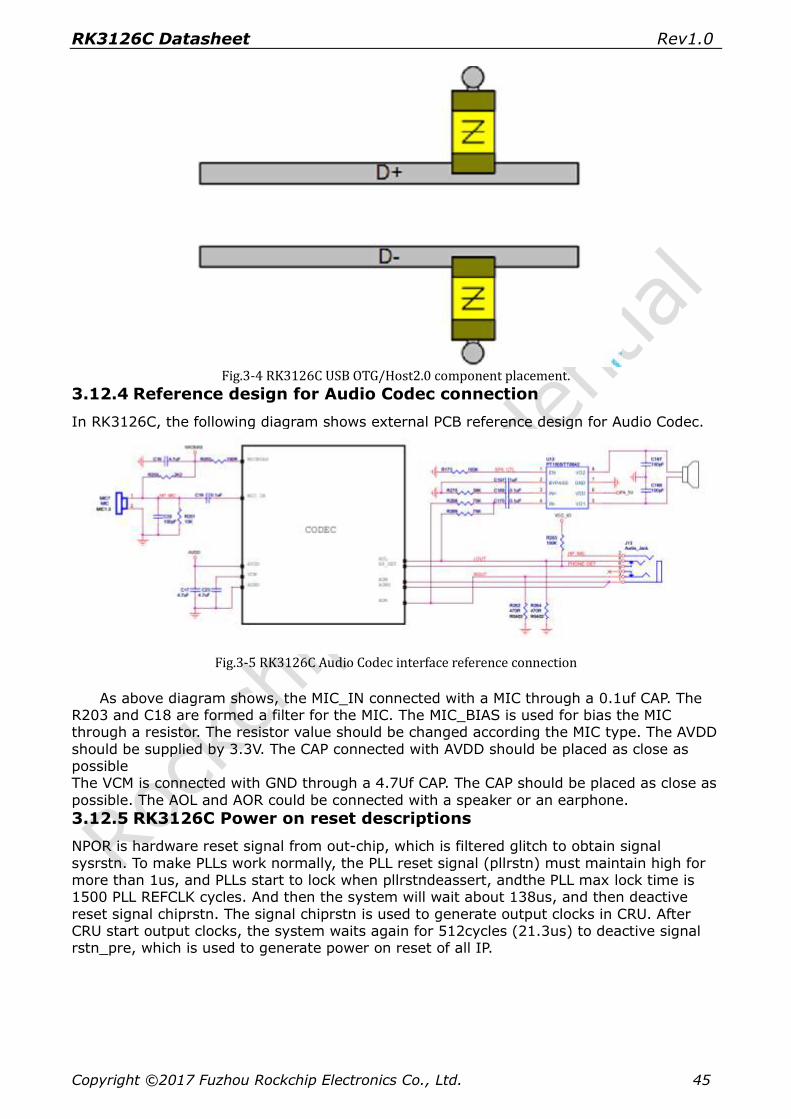
RK3126C Datasheet Rev1.0
Copyright ©2017 Fuzhou Rockchip Electronics Co., Ltd. 45
Fig.3-4 RK3126C USB OTG/Host2.0 component placement.
3.12.4 Reference design for Audio Codec connection
In RK3126C, the following diagram shows external PCB reference design for Audio Codec.
Fig.3-5 RK3126C Audio Codec interface reference connection
As above diagram shows, the MIC_IN connected with a MIC through a 0.1uf CAP. The R203 and C18 are formed a filter for the MIC. The MIC_BIAS is used for bias the MIC through a resistor. The resistor value should be changed according the MIC type. The AVDD
should be supplied by 3.3V. The CAP connected with AVDD should be placed as close as possible The VCM is connected with GND through a 4.7Uf CAP. The CAP should be placed as close as
possible. The AOL and AOR could be connected with a speaker or an earphone.
3.12.5 RK3126C Power on reset descriptions
NPOR is hardware reset signal from out-chip, which is filtered glitch to obtain signal
sysrstn. To make PLLs work normally, the PLL reset signal (pllrstn) must maintain high for more than 1us, and PLLs start to lock when pllrstndeassert, andthe PLL max lock time is 1500 PLL REFCLK cycles. And then the system will wait about 138us, and then deactive
reset signal chiprstn. The signal chiprstn is used to generate output clocks in CRU. After CRU start output clocks, the system waits again for 512cycles (21.3us) to deactive signal rstn_pre, which is used to generate power on reset of all IP.

RK3126C Datasheet Rev1.0
Copyright ©2017 Fuzhou Rockchip Electronics Co., Ltd. 46
npor
sysrstn
pllrstn1.3us
chiprstn138us
rstn_pre(IP reset)
21.3us
Fig.3-6 RK3126C reset signals sequence

RK3126C Datasheet Rev1.0
Copyright ©2017 Fuzhou Rockchip Electronics Co., Ltd. 47
Chapter 4 Thermal Management
4.1 Overview
For reliability and operability concerns, the absolute maximum junction temperature of RK3126C has to be below 125℃.
4.2 Package Thermal Characteristics
Table 4-1 provides the thermal resistance characteristics for the package used on RK3126C. The resulting simulation data for reference only, please prevail in kind test.
Table 4-1 RK3126C Thermal Resistance Characteristics
Package (LQFP)
Power(W) 𝜽𝑱𝑨(℃/𝑾) 𝜽𝑱𝑩(℃/𝑾) 𝜽𝑱𝑪(℃/𝑾)
RK3126C 4.5 15.3 6.70 6.8
Note: The testing PCB is based on 4 layers, 90x90 mm, 1 mm Thickness, ambient temperature is 25℃,