Embed Size (px)
Citation preview
SH79F1622
8051 Microcontroller with 20 channels Touch-key input and TONE
1 V2.2
1. Features 8bits micro-controller with Pipe-line structured 8051
compatible instruction set Flash ROM: 16K Bytes RAM: internal 256 Bytes, external 1280 Bytes Operation Voltage: 2.7V - 5.5V Oscillator:
- Internal RC: 27MHz (±2%) - External crystal oscillator: 32.768kHz
28pin: 25 CMOS bi-directional I/O pins 20pin: 17 CMOS bi-directional I/O pins Built-in pull-up resistor for input pin Three 16-bit timer/counters T2, T3 & T4 20 channels Touch Key input Built-in Touch Key comparison voltage:
1V, 1.5V, 2V, 2.5V 7 COM 16 SEG LED drive
Touch Key sharing with LED drive Powerful interrupt sources:
- Timer2, 3, 4 - INT0, INT1, INT2, INT4 - EUART - Touch Key - TWI
EUART with Baud-rate generator TWI communication interface Built-in 2 channels programmable tone generator CPU Machine cycle: 1 oscillator cycle Watch Dog Timer (WDT) Flash Type Package: SOP28
SOP20 SOP16
2. General Description The SH79F1622 is a high performance 8051 compatible micro-controller, regard to its build-in Pipe-line instruction fetch structure, that helps the SH79F1622 can perform more fast operation speed and higher calculation performance, if compare SH79F1622 with standard 8051 at same clock speed. The SH79F1622 retains most features of the standard 8051. These features include internal 256 bytes RAM, three 16-bit Timer/Counter. In addition, SH79F1622 provides external 1280 bytes RAM, It also contains 16K bytes Flash memory block for storing programs. SH79F1622 also integrate double channels tone generation module, LVR, TWI and Touch Key sharing with LED for saving pins. SH79F1622 is very suitable for the application and control of Touch Key. Also WDT and EUART are incorporated in SH79F1622.
SH79F1622
2
3. Block Diagram
16K BytesFlash ROM
Internal 256 BytesExternal 1280 Bytes
(Exclude System Register)
Oscillator
Pipelined 8051 architecture
Timer 2 (16bit)Timer 3 (16bit)Timer 4(16bit)
v
Reset circuit RST
VDD
External Interrupt
Power
Watch Dog
TONE
Port 3 Configuration I/Os
P1.0 - P1.7
P2.0 - P2.7
P0.0 - P0.7
Port 2 Configuration I/Os
P3.0 `
EUART0
Jtag ports(for debug)
Touch key channel
Port 1 Configuration I/Os
Port 0 Configuration I/Os
TK1-TK20
LED DriverTWI SEG/COM
SH79F1622
3
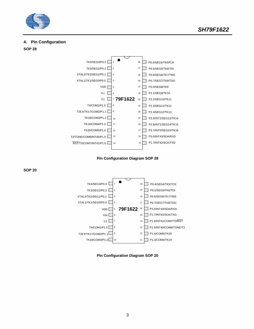
4. Pin Configuration SOP 28
79F1622
1
2
3
4
5
6
7
8
9
10
11
12
13
14
28
27
26
25
24
23
22
21
20
19
18
17
16
15
TK4/SEG3/P0.3
TK3/SEG2/P0.2
XTAL2/TK2/SEG1/P0.1
XTAL1/TK1/SEG0/P0.0
VDD
Vss
C1
T2/TONE/COM6/INT40/P1.5
RST/T3/COM7/INT41/P1.6
P3.0/INT43/SDA/RXD
T4/COM1/P1.0
T2EX/TK17/COM2/P1.1
TK19/COM4/P1.3
TK20/COM5/P1.4 P2.7/INT0/SEG15/TK16
P2.6/INT1/SEG14/TK15
P2.5/INT2/SEG13/TK14
P2.4/SEG12/TK13
P2.3/SEG11/TK12
P2.2/SEG10/TK11
P2.1/SEG9/TK10
P2.0/SEG8/TK9
P0.7/SEG7/TK8/TDO
P0.6/SEG6/TK7/TMS
P0.5/SEG5/TK6/TDI
P0.4/SEG4/TK5/TCK
TK18/COM3/P1.2
P1.7/INT42/SCK/TXD
Pin Configuration Diagram SOP 28
SOP 20
79F1622
1
2
3
4
5
6
7
8
9
10
20
19
18
17
16
15
14
13
12
11
TK4/SEG3/P0.3
TK3/SEG2/P0.2
XTAL2/TK2/SEG1/P0.1
XTAL1/TK1/SEG0/P0.0
VDD
Vss
C1
T4/COM1/P1.0
T2EX/TK17/COM2/P1.1
P1.3/COM4/TK19
P1.4/COM5/TK20
TK18/COM3/P1.2
P0.7/SEG7/TK8/TDO
P0.6/SEG6/TK7/TMS
P0.5/SEG5/TK6/TDI
P0.4/SEG4/TK5/TCK
P1.5/INT40/COM6/TONE/T2
P1.6/INT41/COM7/T3/RST
P3.0/INT43/SDA/RXD
P1.7/INT42/SCK/TXD
Pin Configuration Diagram SOP 20
SH79F1622
4
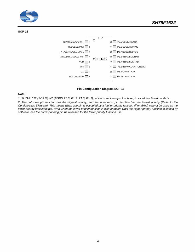
SOP 16
79F1622
1
2
3
4
5
6
7
8
TK3/SEG2/P0.2
XTAL2/TK2/SEG1/P0.1
XTAL1/TK1/SEG0/P0.0
VDD
Vss
C1
P1.5/INT40/COM6/TONE/T2
P3.0/INT43/SDA/RXD
T4/COM1/P1.0 P1.3/COM4/TK19
P1.4/COM5/TK20
P0.7/SEG7/TK8/TDO
P0.6/SEG6/TK7/TMS
P0.5/SEG5/TK6/TDITCK/TK5/SEG4/P0.4
P1.7/INT42/SCK/TXD
9
10
11
12
13
14
15
16
Pin Configuration Diagram SOP 16
Note: 1. SH79F1622 (SOP16) I/O (20PIN P0.3, P1.2, P1.6, P1.1), which is set to output low level, to avoid functional conflicts. 2. The out most pin function has the highest priority, and the inner most pin function has the lowest priority (Refer to Pin Configuration Diagram). This means when one pin is occupied by a higher priority function (if enabled) cannot be used as the lower priority functional pin, even when the lower priority function is also enabled. Until the higher priority function is closed by software, can the corresponding pin be released for the lower priority function use.
SH79F1622
5
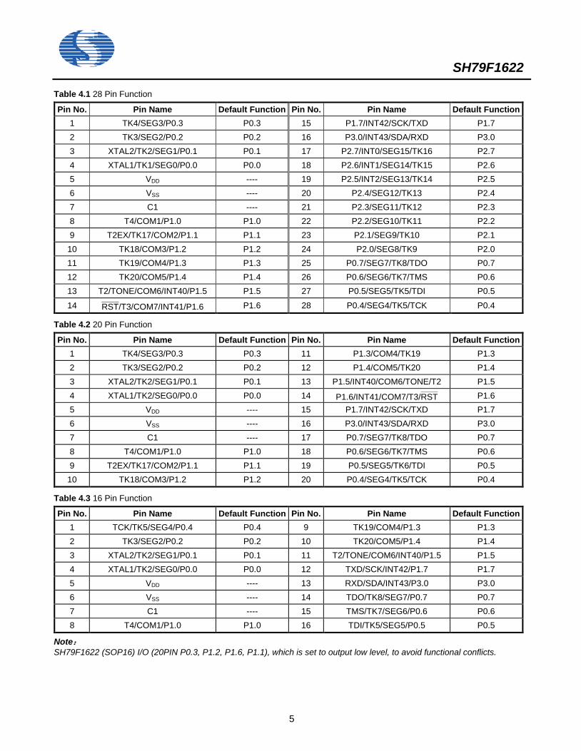
Table 4.1 28 Pin Function
Pin No. Pin Name Default Function Pin No. Pin Name Default Function 1 TK4/SEG3/P0.3 P0.3 15 P1.7/INT42/SCK/TXD P1.7 2 TK3/SEG2/P0.2 P0.2 16 P3.0/INT43/SDA/RXD P3.0 3 XTAL2/TK2/SEG1/P0.1 P0.1 17 P2.7/INT0/SEG15/TK16 P2.7 4 XTAL1/TK1/SEG0/P0.0 P0.0 18 P2.6/INT1/SEG14/TK15 P2.6 5 VDD ---- 19 P2.5/INT2/SEG13/TK14 P2.5 6 VSS ---- 20 P2.4/SEG12/TK13 P2.4 7 C1 ---- 21 P2.3/SEG11/TK12 P2.3 8 T4/COM1/P1.0 P1.0 22 P2.2/SEG10/TK11 P2.2 9 T2EX/TK17/COM2/P1.1 P1.1 23 P2.1/SEG9/TK10 P2.1
10 TK18/COM3/P1.2 P1.2 24 P2.0/SEG8/TK9 P2.0 11 TK19/COM4/P1.3 P1.3 25 P0.7/SEG7/TK8/TDO P0.7 12 TK20/COM5/P1.4 P1.4 26 P0.6/SEG6/TK7/TMS P0.6 13 T2/TONE/COM6/INT40/P1.5 P1.5 27 P0.5/SEG5/TK5/TDI P0.5
14 RST————
/T3/COM7/INT41/P1.6 P1.6 28 P0.4/SEG4/TK5/TCK P0.4
Table 4.2 20 Pin Function
Pin No. Pin Name Default Function Pin No. Pin Name Default Function 1 TK4/SEG3/P0.3 P0.3 11 P1.3/COM4/TK19 P1.3 2 TK3/SEG2/P0.2 P0.2 12 P1.4/COM5/TK20 P1.4 3 XTAL2/TK2/SEG1/P0.1 P0.1 13 P1.5/INT40/COM6/TONE/T2 P1.5 4 XTAL1/TK2/SEG0/P0.0 P0.0 14 P1.6/INT41/COM7/T3/RST
———— P1.6
5 VDD ---- 15 P1.7/INT42/SCK/TXD P1.7 6 VSS ---- 16 P3.0/INT43/SDA/RXD P3.0 7 C1 ---- 17 P0.7/SEG7/TK8/TDO P0.7 8 T4/COM1/P1.0 P1.0 18 P0.6/SEG6/TK7/TMS P0.6 9 T2EX/TK17/COM2/P1.1 P1.1 19 P0.5/SEG5/TK6/TDI P0.5
10 TK18/COM3/P1.2 P1.2 20 P0.4/SEG4/TK5/TCK P0.4
Table 4.3 16 Pin Function
Pin No. Pin Name Default Function Pin No. Pin Name Default Function 1 TCK/TK5/SEG4/P0.4 P0.4 9 TK19/COM4/P1.3 P1.3 2 TK3/SEG2/P0.2 P0.2 10 TK20/COM5/P1.4 P1.4 3 XTAL2/TK2/SEG1/P0.1 P0.1 11 T2/TONE/COM6/INT40/P1.5 P1.5 4 XTAL1/TK2/SEG0/P0.0 P0.0 12 TXD/SCK/INT42/P1.7 P1.7 5 VDD ---- 13 RXD/SDA/INT43/P3.0 P3.0 6 VSS ---- 14 TDO/TK8/SEG7/P0.7 P0.7 7 C1 ---- 15 TMS/TK7/SEG6/P0.6 P0.6 8 T4/COM1/P1.0 P1.0 16 TDI/TK5/SEG5/P0.5 P0.5
Note: SH79F1622 (SOP16) I/O (20PIN P0.3, P1.2, P1.6, P1.1), which is set to output low level, to avoid functional conflicts.
SH79F1622
6
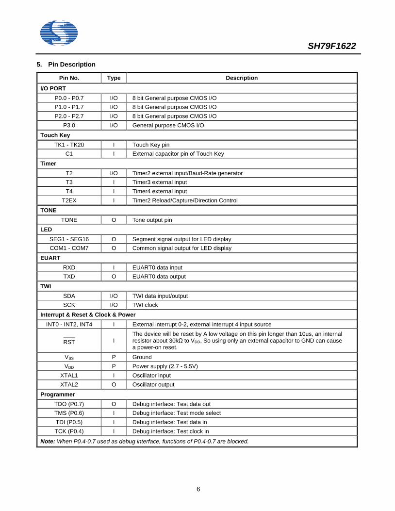
5. Pin Description
Pin No. Type Description
I/O PORT P0.0 - P0.7 I/O 8 bit General purpose CMOS I/O P1.0 - P1.7 I/O 8 bit General purpose CMOS I/O P2.0 - P2.7 I/O 8 bit General purpose CMOS I/O
P3.0 I/O General purpose CMOS I/O
Touch Key TK1 - TK20 I Touch Key pin
C1 I External capacitor pin of Touch Key
Timer T2 I/O Timer2 external input/Baud-Rate generator T3 I Timer3 external input T4 I Timer4 external input
T2EX I Timer2 Reload/Capture/Direction Control
TONE TONE O Tone output pin
LED SEG1 - SEG16 O Segment signal output for LED display COM1 - COM7 O Common signal output for LED display
EUART RXD I EUART0 data input TXD O EUART0 data output
TWI SDA I/O TWI data input/output SCK I/O TWI clock
Interrupt & Reset & Clock & Power INT0 - INT2, INT4 I External interrupt 0-2, external interrupt 4 input source
RST————
I The device will be reset by A low voltage on this pin longer than 10us, an internal resistor about 30kΩ to VDD, So using only an external capacitor to GND can cause a power-on reset.
VSS P Ground VDD P Power supply (2.7 - 5.5V)
XTAL1 I Oscillator input XTAL2 O Oscillator output
Programmer TDO (P0.7) O Debug interface: Test data out TMS (P0.6) I Debug interface: Test mode select TDI (P0.5) I Debug interface: Test data in TCK (P0.4) I Debug interface: Test clock in
Note: When P0.4-0.7 used as debug interface, functions of P0.4-0.7 are blocked.
SH79F1622
7
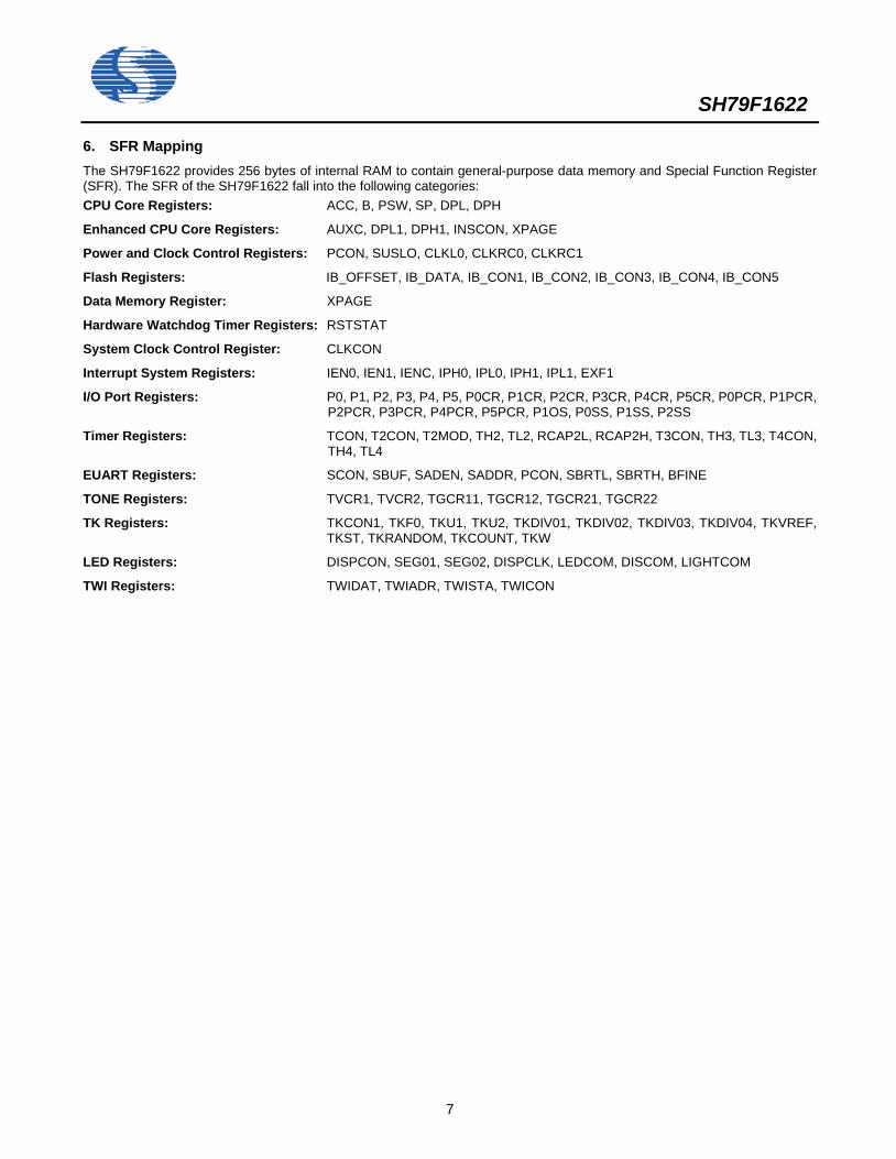
6. SFR Mapping The SH79F1622 provides 256 bytes of internal RAM to contain general-purpose data memory and Special Function Register (SFR). The SFR of the SH79F1622 fall into the following categories: CPU Core Registers: ACC, B, PSW, SP, DPL, DPH
Enhanced CPU Core Registers: AUXC, DPL1, DPH1, INSCON, XPAGE
Power and Clock Control Registers: PCON, SUSLO, CLKL0, CLKRC0, CLKRC1
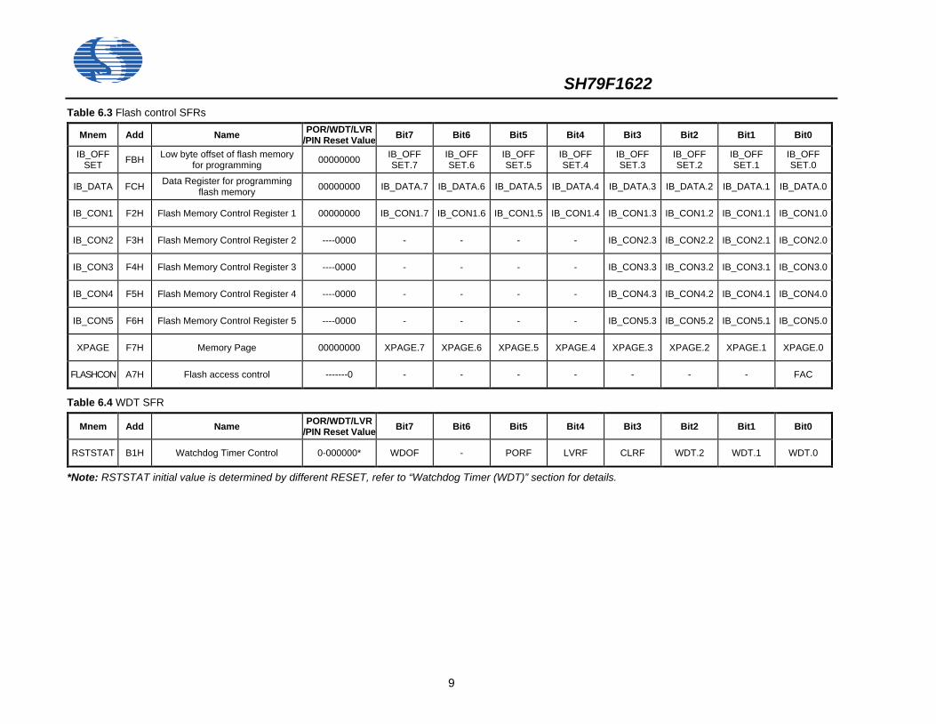
Flash Registers: IB_OFFSET, IB_DATA, IB_CON1, IB_CON2, IB_CON3, IB_CON4, IB_CON5
Data Memory Register: XPAGE
Hardware Watchdog Timer Registers: RSTSTAT
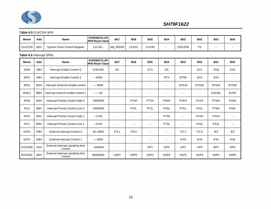
System Clock Control Register: CLKCON
Interrupt System Registers: IEN0, IEN1, IENC, IPH0, IPL0, IPH1, IPL1, EXF1
I/O Port Registers: P0, P1, P2, P3, P4, P5, P0CR, P1CR, P2CR, P3CR, P4CR, P5CR, P0PCR, P1PCR, P2PCR, P3PCR, P4PCR, P5PCR, P1OS, P0SS, P1SS, P2SS
Timer Registers: TCON, T2CON, T2MOD, TH2, TL2, RCAP2L, RCAP2H, T3CON, TH3, TL3, T4CON, TH4, TL4
EUART Registers: SCON, SBUF, SADEN, SADDR, PCON, SBRTL, SBRTH, BFINE
TONE Registers: TVCR1, TVCR2, TGCR11, TGCR12, TGCR21, TGCR22
TK Registers: TKCON1, TKF0, TKU1, TKU2, TKDIV01, TKDIV02, TKDIV03, TKDIV04, TKVREF, TKST, TKRANDOM, TKCOUNT, TKW
LED Registers: DISPCON, SEG01, SEG02, DISPCLK, LEDCOM, DISCOM, LIGHTCOM
TWI Registers: TWIDAT, TWIADR, TWISTA, TWICON
SH79F1622
8
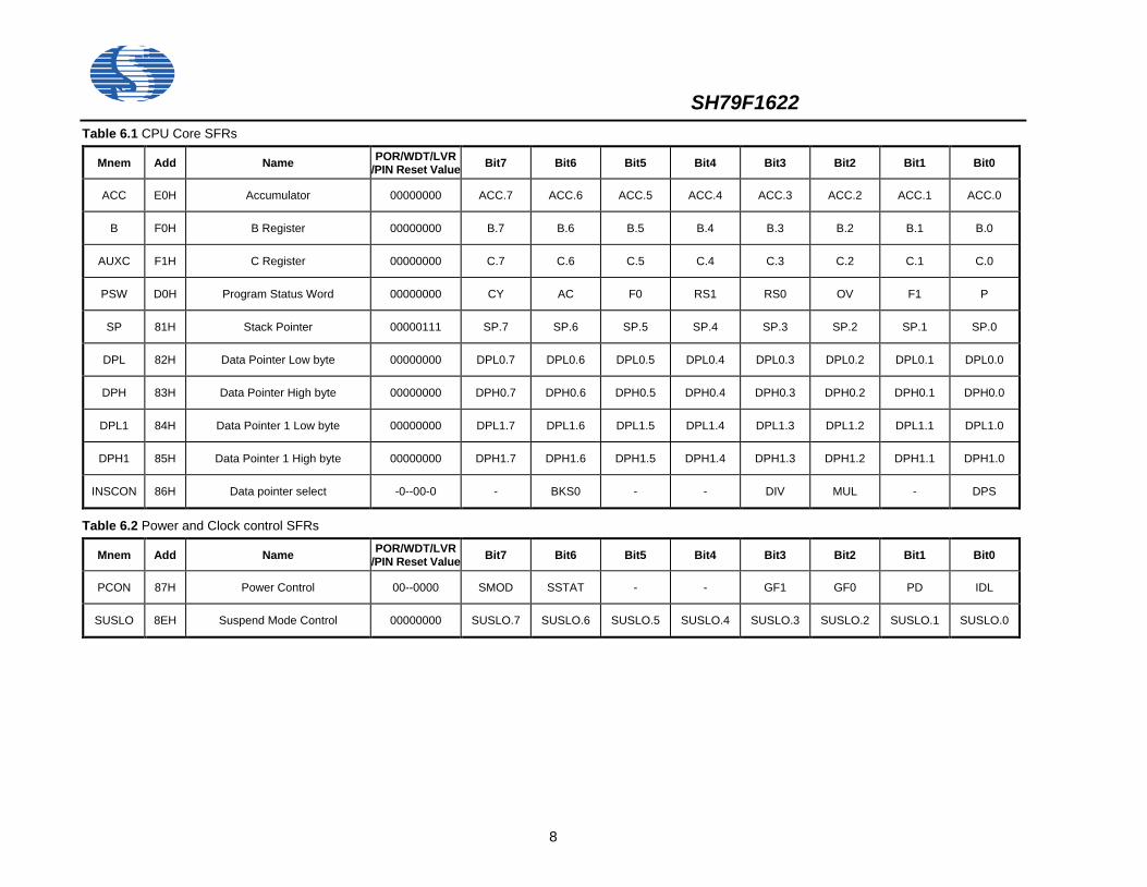
Table 6.1 CPU Core SFRs
Mnem Add Name POR/WDT/LVR /PIN Reset Value Bit7 Bit6 Bit5 Bit4 Bit3 Bit2 Bit1 Bit0
ACC E0H Accumulator 00000000 ACC.7 ACC.6 ACC.5 ACC.4 ACC.3 ACC.2 ACC.1 ACC.0
B F0H B Register 00000000 B.7 B.6 B.5 B.4 B.3 B.2 B.1 B.0
AUXC F1H C Register 00000000 C.7 C.6 C.5 C.4 C.3 C.2 C.1 C.0
PSW D0H Program Status Word 00000000 CY AC F0 RS1 RS0 OV F1 P
SP 81H Stack Pointer 00000111 SP.7 SP.6 SP.5 SP.4 SP.3 SP.2 SP.1 SP.0
DPL 82H Data Pointer Low byte 00000000 DPL0.7 DPL0.6 DPL0.5 DPL0.4 DPL0.3 DPL0.2 DPL0.1 DPL0.0
DPH 83H Data Pointer High byte 00000000 DPH0.7 DPH0.6 DPH0.5 DPH0.4 DPH0.3 DPH0.2 DPH0.1 DPH0.0
DPL1 84H Data Pointer 1 Low byte 00000000 DPL1.7 DPL1.6 DPL1.5 DPL1.4 DPL1.3 DPL1.2 DPL1.1 DPL1.0
DPH1 85H Data Pointer 1 High byte 00000000 DPH1.7 DPH1.6 DPH1.5 DPH1.4 DPH1.3 DPH1.2 DPH1.1 DPH1.0
INSCON 86H Data pointer select -0--00-0 - BKS0 - - DIV MUL - DPS
Table 6.2 Power and Clock control SFRs
Mnem Add Name POR/WDT/LVR /PIN Reset Value Bit7 Bit6 Bit5 Bit4 Bit3 Bit2 Bit1 Bit0
PCON 87H Power Control 00--0000 SMOD SSTAT - - GF1 GF0 PD IDL
SUSLO 8EH Suspend Mode Control 00000000 SUSLO.7 SUSLO.6 SUSLO.5 SUSLO.4 SUSLO.3 SUSLO.2 SUSLO.1 SUSLO.0
SH79F1622
9
Table 6.3 Flash control SFRs
Mnem Add Name POR/WDT/LVR /PIN Reset Value Bit7 Bit6 Bit5 Bit4 Bit3 Bit2 Bit1 Bit0
IB_OFF SET FBH Low byte offset of flash memory
for programming 00000000 IB_OFF SET.7
IB_OFF SET.6
IB_OFF SET.5
IB_OFF SET.4
IB_OFF SET.3
IB_OFF SET.2
IB_OFF SET.1
IB_OFF SET.0
IB_DATA FCH Data Register for programming flash memory 00000000 IB_DATA.7 IB_DATA.6 IB_DATA.5 IB_DATA.4 IB_DATA.3 IB_DATA.2 IB_DATA.1 IB_DATA.0
IB_CON1 F2H Flash Memory Control Register 1 00000000 IB_CON1.7 IB_CON1.6 IB_CON1.5 IB_CON1.4 IB_CON1.3 IB_CON1.2 IB_CON1.1 IB_CON1.0
IB_CON2 F3H Flash Memory Control Register 2 ----0000 - - - - IB_CON2.3 IB_CON2.2 IB_CON2.1 IB_CON2.0
IB_CON3 F4H Flash Memory Control Register 3 ----0000 - - - - IB_CON3.3 IB_CON3.2 IB_CON3.1 IB_CON3.0
IB_CON4 F5H Flash Memory Control Register 4 ----0000 - - - - IB_CON4.3 IB_CON4.2 IB_CON4.1 IB_CON4.0
IB_CON5 F6H Flash Memory Control Register 5 ----0000 - - - - IB_CON5.3 IB_CON5.2 IB_CON5.1 IB_CON5.0
XPAGE F7H Memory Page 00000000 XPAGE.7 XPAGE.6 XPAGE.5 XPAGE.4 XPAGE.3 XPAGE.2 XPAGE.1 XPAGE.0
FLASHCON A7H Flash access control -------0 - - - - - - - FAC
Table 6.4 WDT SFR
Mnem Add Name POR/WDT/LVR /PIN Reset Value Bit7 Bit6 Bit5 Bit4 Bit3 Bit2 Bit1 Bit0
RSTSTAT B1H Watchdog Timer Control 0-000000* WDOF - PORF LVRF CLRF WDT.2 WDT.1 WDT.0
*Note: RSTSTAT initial value is determined by different RESET, refer to “Watchdog Timer (WDT)” section for details.
SH79F1622
10
Table 6.5 CLKCON SFR
Mnem Add Name POR/WDT/LVR /PIN Reset Value Bit7 Bit6 Bit5 Bit4 Bit3 Bit2 Bit1 Bit0
CLKCON B2H System Clock Control Register 111-00-- 32k_SPDUP CLKS1 CLKS0 - OSC2ON FS - -
Table 6.6 Interrupt SFRs
Mnem Add Name POR/WDT/LVR /PIN Reset Value Bit7 Bit6 Bit5 Bit4 Bit3 Bit2 Bit1 Bit0
IEN0 A8H Interrupt Enable Control 0 0-00-000 EA - ET2 ES - EX1 TKIE EX0
IEN1 A9H Interrupt Enable Control 1 ---0000- - - - ET3 ETWI EX3 EX2 -
IENC BAH Interrupt 4channel enable control ----0000 - - - - EXS43 EXS42 EXS41 EXS40
IENC1 BBH Interrupt channel enable control 1 ------00 - - - - - - ESCM1 ELPD
IPH0 B4H Interrupt Priority Control High 0 -0000000 - PT4H PT2H PS0H PTKH PX1H PTWH PX0H
IPL0 B8H Interrupt Priority Control Low 0 -0000000 - PT4L PT2L PS0L PTKL PX1L PTWL PX0L
IPH1 B5H Interrupt Priority Control High 1 ---0-00- - - - PT3H - PX4H PX2H -
IPL1 B9H Interrupt Priority Control Low 1 ---0-00- - - - PT3L - PX4L PX2L -
EXF0 E8H External interrupt Control 0 00--0000 IT4.1 IT4.0 - - IT2.1 IT2.0 IE3 IE2
EXF1 D8H External interrupt Control 1 ----0000 - - - - IF43 IF42 IF41 IF40
EXCON0 ADH External interrupt sampling time Control --000000 - - I2P1 I2P0 I1P1 I1P0 I0P1 I0P0
EXCON1 AEH External interrupt sampling time Control 00000000 I43P1 I43P0 I42P1 I42P0 I41P1 I41P0 I40P1 I40P0
SH79F1622
11
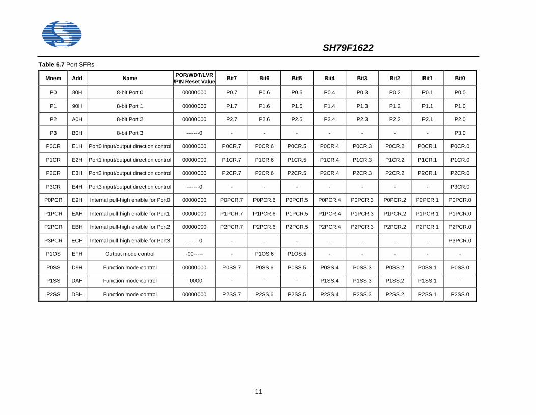
Table 6.7 Port SFRs
Mnem Add Name POR/WDT/LVR /PIN Reset Value Bit7 Bit6 Bit5 Bit4 Bit3 Bit2 Bit1 Bit0
P0 80H 8-bit Port 0 00000000 P0.7 P0.6 P0.5 P0.4 P0.3 P0.2 P0.1 P0.0
P1 90H 8-bit Port 1 00000000 P1.7 P1.6 P1.5 P1.4 P1.3 P1.2 P1.1 P1.0
P2 A0H 8-bit Port 2 00000000 P2.7 P2.6 P2.5 P2.4 P2.3 P2.2 P2.1 P2.0
P3 B0H 8-bit Port 3 -------0 - - - - - - - P3.0
P0CR E1H Port0 input/output direction control 00000000 P0CR.7 P0CR.6 P0CR.5 P0CR.4 P0CR.3 P0CR.2 P0CR.1 P0CR.0
P1CR E2H Port1 input/output direction control 00000000 P1CR.7 P1CR.6 P1CR.5 P1CR.4 P1CR.3 P1CR.2 P1CR.1 P1CR.0
P2CR E3H Port2 input/output direction control 00000000 P2CR.7 P2CR.6 P2CR.5 P2CR.4 P2CR.3 P2CR.2 P2CR.1 P2CR.0
P3CR E4H Port3 input/output direction control -------0 - - - - - - - P3CR.0
P0PCR E9H Internal pull-high enable for Port0 00000000 P0PCR.7 P0PCR.6 P0PCR.5 P0PCR.4 P0PCR.3 P0PCR.2 P0PCR.1 P0PCR.0
P1PCR EAH Internal pull-high enable for Port1 00000000 P1PCR.7 P1PCR.6 P1PCR.5 P1PCR.4 P1PCR.3 P1PCR.2 P1PCR.1 P1PCR.0
P2PCR EBH Internal pull-high enable for Port2 00000000 P2PCR.7 P2PCR.6 P2PCR.5 P2PCR.4 P2PCR.3 P2PCR.2 P2PCR.1 P2PCR.0
P3PCR ECH Internal pull-high enable for Port3 -------0 - - - - - - - P3PCR.0
P1OS EFH Output mode control -00----- - P1OS.6 P1OS.5 - - - - -
P0SS D9H Function mode control 00000000 P0SS.7 P0SS.6 P0SS.5 P0SS.4 P0SS.3 P0SS.2 P0SS.1 P0SS.0
P1SS DAH Function mode control ---0000- - - - P1SS.4 P1SS.3 P1SS.2 P1SS.1 -
P2SS DBH Function mode control 00000000 P2SS.7 P2SS.6 P2SS.5 P2SS.4 P2SS.3 P2SS.2 P2SS.1 P2SS.0
SH79F1622
12
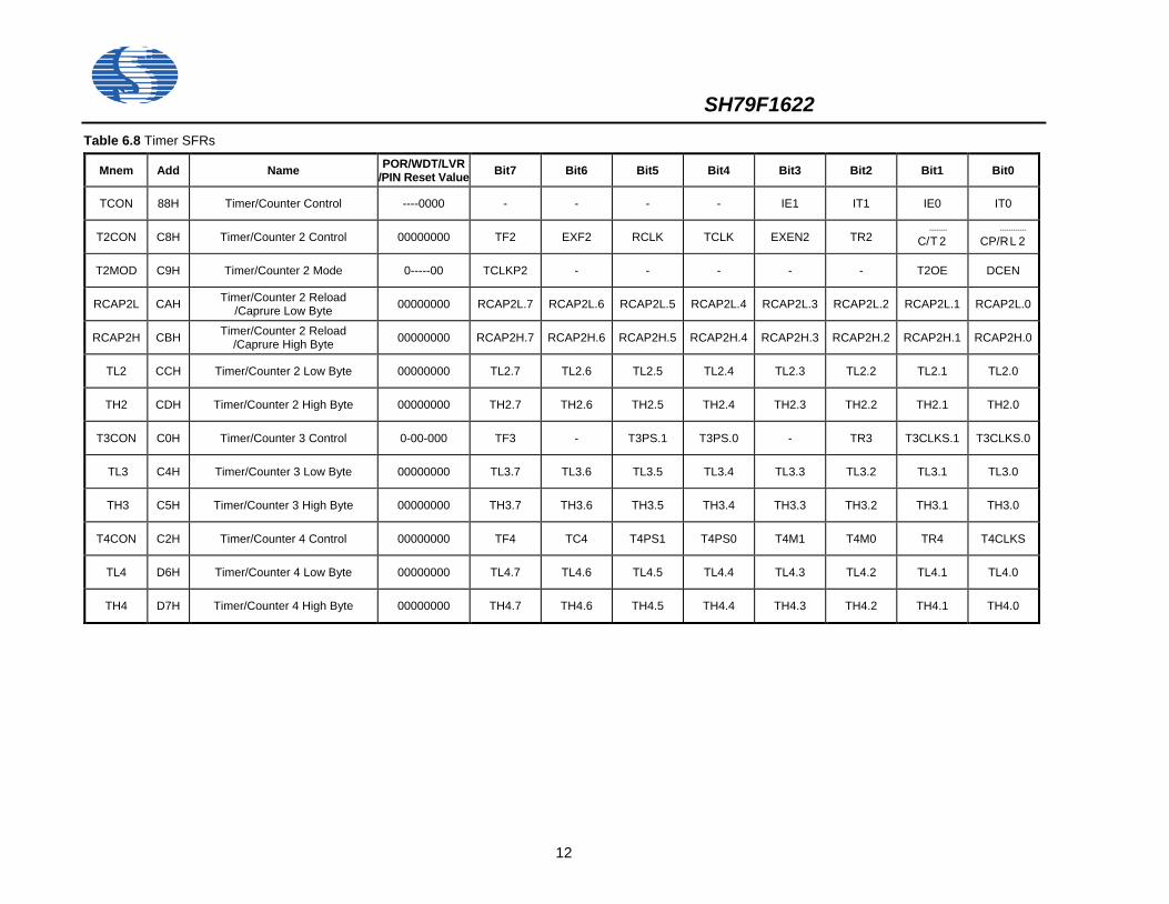
Table 6.8 Timer SFRs
Mnem Add Name POR/WDT/LVR /PIN Reset Value Bit7 Bit6 Bit5 Bit4 Bit3 Bit2 Bit1 Bit0
TCON 88H Timer/Counter Control ----0000 - - - - IE1 IT1 IE0 IT0
T2CON C8H Timer/Counter 2 Control 00000000 TF2 EXF2 RCLK TCLK EXEN2 TR2 C/T----
2----
CP/R----
L----
2----
T2MOD C9H Timer/Counter 2 Mode 0-----00 TCLKP2 - - - - - T2OE DCEN
RCAP2L CAH Timer/Counter 2 Reload /Caprure Low Byte 00000000 RCAP2L.7 RCAP2L.6 RCAP2L.5 RCAP2L.4 RCAP2L.3 RCAP2L.2 RCAP2L.1 RCAP2L.0
RCAP2H CBH Timer/Counter 2 Reload /Caprure High Byte 00000000 RCAP2H.7 RCAP2H.6 RCAP2H.5 RCAP2H.4 RCAP2H.3 RCAP2H.2 RCAP2H.1 RCAP2H.0
TL2 CCH Timer/Counter 2 Low Byte 00000000 TL2.7 TL2.6 TL2.5 TL2.4 TL2.3 TL2.2 TL2.1 TL2.0
TH2 CDH Timer/Counter 2 High Byte 00000000 TH2.7 TH2.6 TH2.5 TH2.4 TH2.3 TH2.2 TH2.1 TH2.0
T3CON C0H Timer/Counter 3 Control 0-00-000 TF3 - T3PS.1 T3PS.0 - TR3 T3CLKS.1 T3CLKS.0
TL3 C4H Timer/Counter 3 Low Byte 00000000 TL3.7 TL3.6 TL3.5 TL3.4 TL3.3 TL3.2 TL3.1 TL3.0
TH3 C5H Timer/Counter 3 High Byte 00000000 TH3.7 TH3.6 TH3.5 TH3.4 TH3.3 TH3.2 TH3.1 TH3.0
T4CON C2H Timer/Counter 4 Control 00000000 TF4 TC4 T4PS1 T4PS0 T4M1 T4M0 TR4 T4CLKS
TL4 D6H Timer/Counter 4 Low Byte 00000000 TL4.7 TL4.6 TL4.5 TL4.4 TL4.3 TL4.2 TL4.1 TL4.0
TH4 D7H Timer/Counter 4 High Byte 00000000 TH4.7 TH4.6 TH4.5 TH4.4 TH4.3 TH4.2 TH4.1 TH4.0
SH79F1622
13
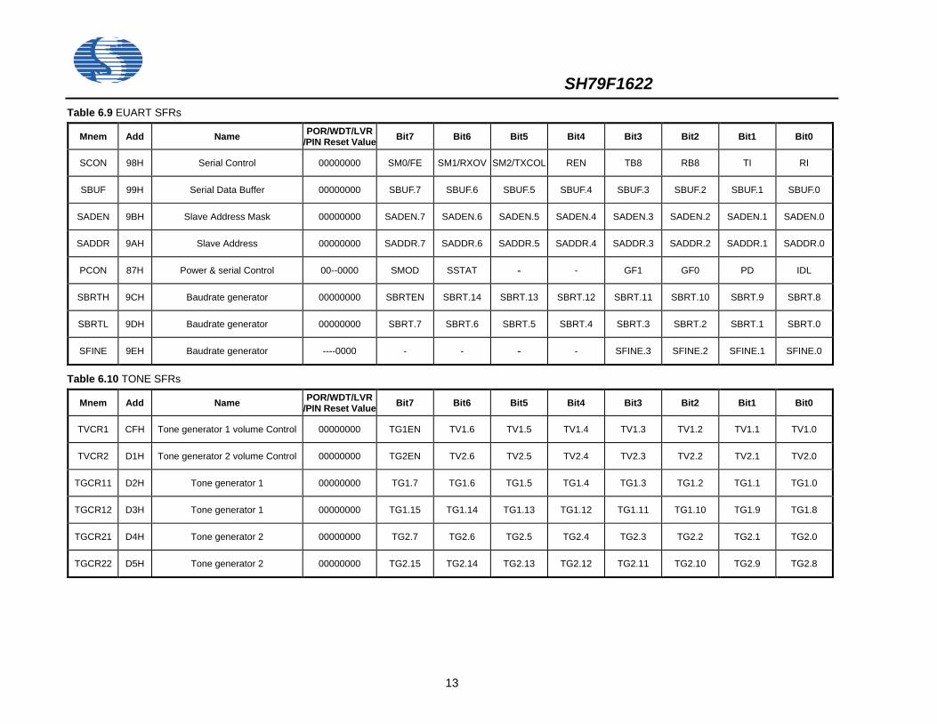
Table 6.9 EUART SFRs
Mnem Add Name POR/WDT/LVR /PIN Reset Value Bit7 Bit6 Bit5 Bit4 Bit3 Bit2 Bit1 Bit0
SCON 98H Serial Control 00000000 SM0/FE SM1/RXOV SM2/TXCOL REN TB8 RB8 TI RI
SBUF 99H Serial Data Buffer 00000000 SBUF.7 SBUF.6 SBUF.5 SBUF.4 SBUF.3 SBUF.2 SBUF.1 SBUF.0
SADEN 9BH Slave Address Mask 00000000 SADEN.7 SADEN.6 SADEN.5 SADEN.4 SADEN.3 SADEN.2 SADEN.1 SADEN.0
SADDR 9AH Slave Address 00000000 SADDR.7 SADDR.6 SADDR.5 SADDR.4 SADDR.3 SADDR.2 SADDR.1 SADDR.0
PCON 87H Power & serial Control 00--0000 SMOD SSTAT - - GF1 GF0 PD IDL
SBRTH 9CH Baudrate generator 00000000 SBRTEN SBRT.14 SBRT.13 SBRT.12 SBRT.11 SBRT.10 SBRT.9 SBRT.8
SBRTL 9DH Baudrate generator 00000000 SBRT.7 SBRT.6 SBRT.5 SBRT.4 SBRT.3 SBRT.2 SBRT.1 SBRT.0
SFINE 9EH Baudrate generator ----0000 - - - - SFINE.3 SFINE.2 SFINE.1 SFINE.0
Table 6.10 TONE SFRs
Mnem Add Name POR/WDT/LVR /PIN Reset Value Bit7 Bit6 Bit5 Bit4 Bit3 Bit2 Bit1 Bit0
TVCR1 CFH Tone generator 1 volume Control 00000000 TG1EN TV1.6 TV1.5 TV1.4 TV1.3 TV1.2 TV1.1 TV1.0
TVCR2 D1H Tone generator 2 volume Control 00000000 TG2EN TV2.6 TV2.5 TV2.4 TV2.3 TV2.2 TV2.1 TV2.0
TGCR11 D2H Tone generator 1 00000000 TG1.7 TG1.6 TG1.5 TG1.4 TG1.3 TG1.2 TG1.1 TG1.0
TGCR12 D3H Tone generator 1 00000000 TG1.15 TG1.14 TG1.13 TG1.12 TG1.11 TG1.10 TG1.9 TG1.8
TGCR21 D4H Tone generator 2 00000000 TG2.7 TG2.6 TG2.5 TG2.4 TG2.3 TG2.2 TG2.1 TG2.0
TGCR22 D5H Tone generator 2 00000000 TG2.15 TG2.14 TG2.13 TG2.12 TG2.11 TG2.10 TG2.9 TG2.8
SH79F1622
14
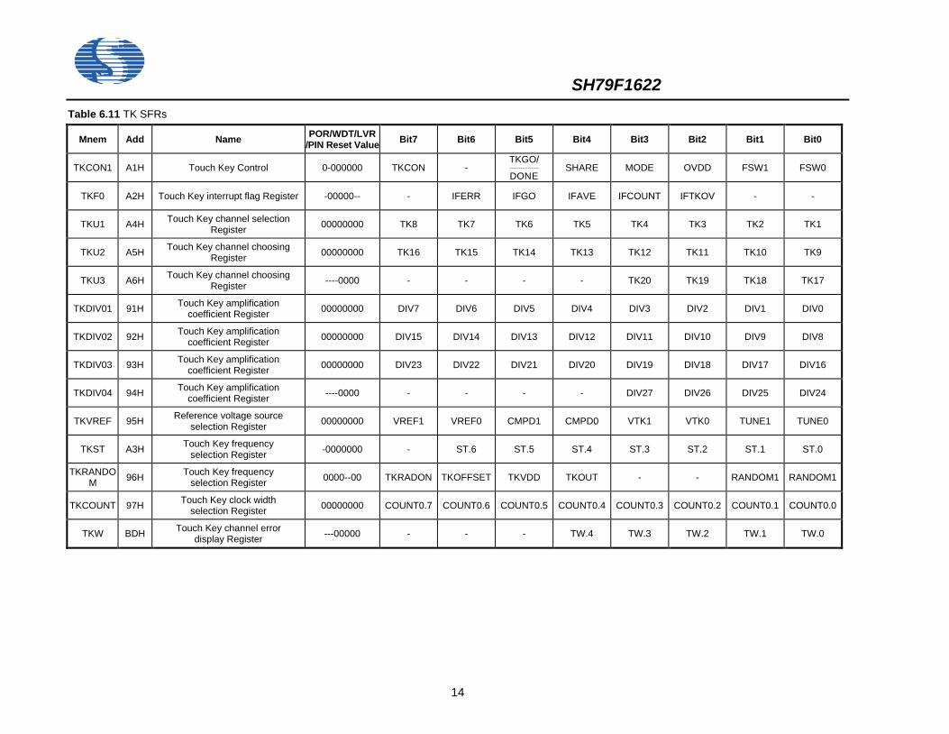
Table 6.11 TK SFRs
Mnem Add Name POR/WDT/LVR /PIN Reset Value Bit7 Bit6 Bit5 Bit4 Bit3 Bit2 Bit1 Bit0
TKCON1 A1H Touch Key Control 0-000000 TKCON - TKGO/
D----
O----
N----
E----
SHARE MODE OVDD FSW1 FSW0
TKF0 A2H Touch Key interrupt flag Register -00000-- - IFERR IFGO IFAVE IFCOUNT IFTKOV - -
TKU1 A4H Touch Key channel selection Register 00000000 TK8 TK7 TK6 TK5 TK4 TK3 TK2 TK1
TKU2 A5H Touch Key channel choosing Register 00000000 TK16 TK15 TK14 TK13 TK12 TK11 TK10 TK9
TKU3 A6H Touch Key channel choosing Register ----0000 - - - - TK20 TK19 TK18 TK17
TKDIV01 91H Touch Key amplification coefficient Register 00000000 DIV7 DIV6 DIV5 DIV4 DIV3 DIV2 DIV1 DIV0
TKDIV02 92H Touch Key amplification coefficient Register 00000000 DIV15 DIV14 DIV13 DIV12 DIV11 DIV10 DIV9 DIV8
TKDIV03 93H Touch Key amplification coefficient Register 00000000 DIV23 DIV22 DIV21 DIV20 DIV19 DIV18 DIV17 DIV16
TKDIV04 94H Touch Key amplification coefficient Register ----0000 - - - - DIV27 DIV26 DIV25 DIV24
TKVREF 95H Reference voltage source selection Register 00000000 VREF1 VREF0 CMPD1 CMPD0 VTK1 VTK0 TUNE1 TUNE0
TKST A3H Touch Key frequency selection Register -0000000 - ST.6 ST.5 ST.4 ST.3 ST.2 ST.1 ST.0
TKRANDOM 96H Touch Key frequency
selection Register 0000--00 TKRADON TKOFFSET TKVDD TKOUT - - RANDOM1 RANDOM1
TKCOUNT 97H Touch Key clock width selection Register 00000000 COUNT0.7 COUNT0.6 COUNT0.5 COUNT0.4 COUNT0.3 COUNT0.2 COUNT0.1 COUNT0.0
TKW BDH Touch Key channel error display Register ---00000 - - - TW.4 TW.3 TW.2 TW.1 TW.0
SH79F1622
15
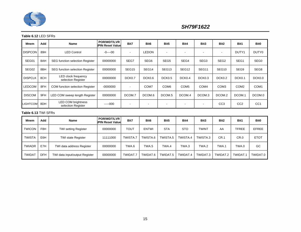
Table 6.12 LED SFRs
Mnem Add Name POR/WDT/LVR /PIN Reset Value Bit7 Bit6 Bit5 Bit4 Bit3 Bit2 Bit1 Bit0
DISPCON 89H LED Control -0----00 - LEDON - - - - DUTY1 DUTY0
SEG01 8AH SEG function selection Register 00000000 SEG7 SEG6 SEG5 SEG4 SEG3 SEG2 SEG1 SEG0
SEG02 8BH SEG function selection Register 00000000 SEG15 SEG14 SEG13 SEG12 SEG11 SEG10 SEG9 SEG8
DISPCLK 8CH LED clock frequency selection Register 00000000 DCK0.7 DCK0.6 DCK0.5 DCK0.4 DCK0.3 DCK0.2 DCK0.1 DCK0.0
LEDCOM 8FH COM function selection Register -0000000 - COM7 COM6 COM5 COM4 COM3 COM2 COM1
DISCOM 9FH LED COM sweep length Register 00000000 DCOM.7 DCOM.6 DCOM.5 DCOM.4 DCOM.3 DCOM.2 DCOM.1 DCOM.0
LIGHTCOM 8DH LED COM brightness selection Register -----000 - - - - - CC3 CC2 CC1
Table 6.13 TWI SFRs
Mnem Add Name POR/WDT/LVR /PIN Reset Value Bit7 Bit6 Bit5 Bit4 Bit3 Bit2 Bit1 Bit0
TWICON F8H TWI setting Register 00000000 TOUT ENTWI STA STO TWINT AA TFREE EFREE
TWISTA E6H TWI state Register 11111000 TWISTA.7 TWISTA.6 TWISTA.5 TWISTA.4 TWISTA.3 CR.1 CR.0 ETOT
TWIADR E7H TWI data address Register 00000000 TWA.6 TWA.5 TWA.4 TWA.3 TWA.2 TWA.1 TWA.0 GC
TWIDAT DFH TWI data input/output Register 00000000 TWIDAT.7 TWIDAT.6 TWIDAT.5 TWIDAT.4 TWIDAT.3 TWIDAT.2 TWIDAT.1 TWIDAT.0
SH79F1622
16
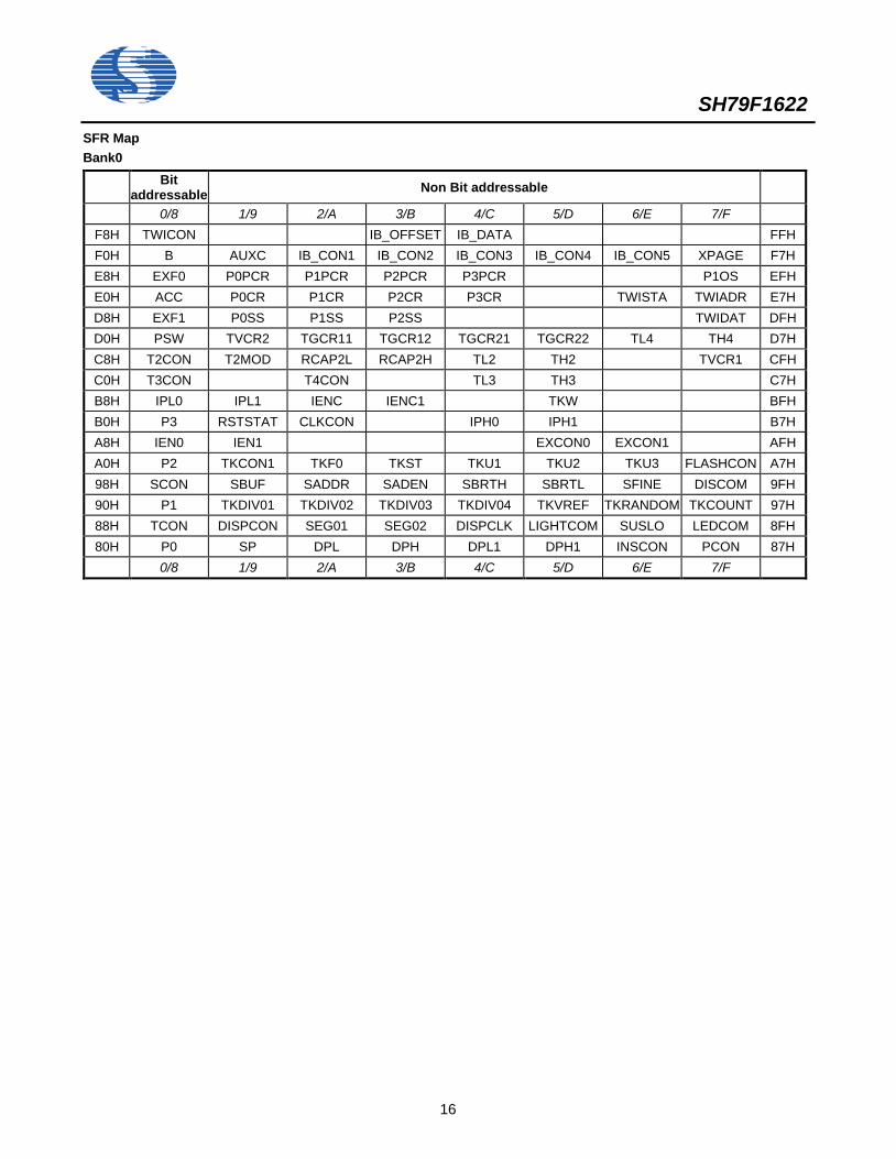
SFR Map Bank0
Bit addressable Non Bit addressable
0/8 1/9 2/A 3/B 4/C 5/D 6/E 7/F F8H TWICON IB_OFFSET IB_DATA FFH F0H B AUXC IB_CON1 IB_CON2 IB_CON3 IB_CON4 IB_CON5 XPAGE F7H E8H EXF0 P0PCR P1PCR P2PCR P3PCR P1OS EFH E0H ACC P0CR P1CR P2CR P3CR TWISTA TWIADR E7H D8H EXF1 P0SS P1SS P2SS TWIDAT DFH D0H PSW TVCR2 TGCR11 TGCR12 TGCR21 TGCR22 TL4 TH4 D7H C8H T2CON T2MOD RCAP2L RCAP2H TL2 TH2 TVCR1 CFH C0H T3CON T4CON TL3 TH3 C7H B8H IPL0 IPL1 IENC IENC1 TKW BFH B0H P3 RSTSTAT CLKCON IPH0 IPH1 B7H A8H IEN0 IEN1 EXCON0 EXCON1 AFH A0H P2 TKCON1 TKF0 TKST TKU1 TKU2 TKU3 FLASHCON A7H 98H SCON SBUF SADDR SADEN SBRTH SBRTL SFINE DISCOM 9FH 90H P1 TKDIV01 TKDIV02 TKDIV03 TKDIV04 TKVREF TKRANDOM TKCOUNT 97H 88H TCON DISPCON SEG01 SEG02 DISPCLK LIGHTCOM SUSLO LEDCOM 8FH 80H P0 SP DPL DPH DPL1 DPH1 INSCON PCON 87H
0/8 1/9 2/A 3/B 4/C 5/D 6/E 7/F
SH79F1622
17
7. Normal Function 7.1 CPU 7.1.1 CPU Core SFR Feature
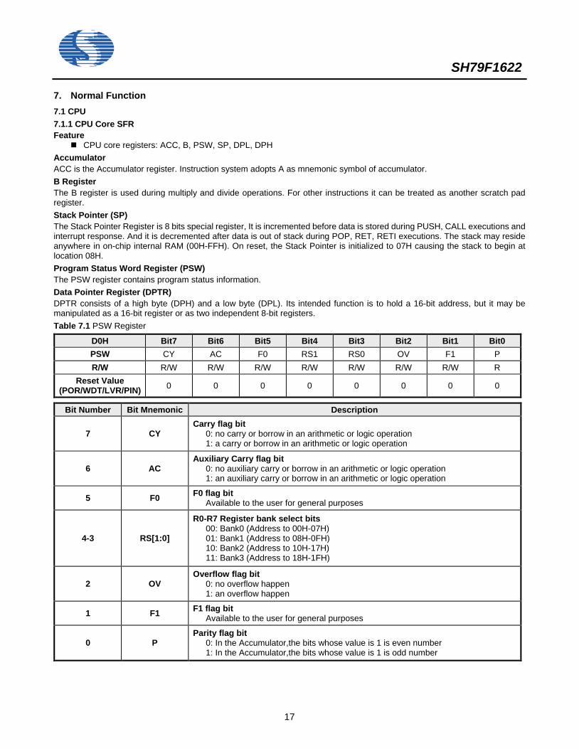
CPU core registers: ACC, B, PSW, SP, DPL, DPH Accumulator ACC is the Accumulator register. Instruction system adopts A as mnemonic symbol of accumulator. B Register The B register is used during multiply and divide operations. For other instructions it can be treated as another scratch pad register. Stack Pointer (SP) The Stack Pointer Register is 8 bits special register, It is incremented before data is stored during PUSH, CALL executions and interrupt response. And it is decremented after data is out of stack during POP, RET, RETI executions. The stack may reside anywhere in on-chip internal RAM (00H-FFH). On reset, the Stack Pointer is initialized to 07H causing the stack to begin at location 08H. Program Status Word Register (PSW) The PSW register contains program status information. Data Pointer Register (DPTR) DPTR consists of a high byte (DPH) and a low byte (DPL). Its intended function is to hold a 16-bit address, but it may be manipulated as a 16-bit register or as two independent 8-bit registers. Table 7.1 PSW Register
D0H Bit7 Bit6 Bit5 Bit4 Bit3 Bit2 Bit1 Bit0 PSW CY AC F0 RS1 RS0 OV F1 P R/W R/W R/W R/W R/W R/W R/W R/W R
Reset Value (POR/WDT/LVR/PIN) 0 0 0 0 0 0 0 0
Bit Number Bit Mnemonic Description
7 CY Carry flag bit
0: no carry or borrow in an arithmetic or logic operation 1: a carry or borrow in an arithmetic or logic operation
6 AC Auxiliary Carry flag bit
0: no auxiliary carry or borrow in an arithmetic or logic operation 1: an auxiliary carry or borrow in an arithmetic or logic operation
5 F0 F0 flag bit Available to the user for general purposes
4-3 RS[1:0]
R0-R7 Register bank select bits 00: Bank0 (Address to 00H-07H) 01: Bank1 (Address to 08H-0FH) 10: Bank2 (Address to 10H-17H) 11: Bank3 (Address to 18H-1FH)
2 OV Overflow flag bit
0: no overflow happen 1: an overflow happen
1 F1 F1 flag bit Available to the user for general purposes
0 P Parity flag bit
0: In the Accumulator,the bits whose value is 1 is even number 1: In the Accumulator,the bits whose value is 1 is odd number
SH79F1622
18
7.1.2 Enhanced CPU core SFRs
Extended 'MUL' and 'DIV' instructions: 16bit*8bit, 16bit/8bit Dual Data Pointer Enhanced CPU core registers: AUXC, DPL1, DPH1, INSCON
The SH79F1622 has modified 'MUL' and 'DIV' instructions. These instructions support 16 bit operand. A new register - the register AUXC is applied to hold the upper part of the operand/result. The AUXC register is used during 16 bit operand multiply and divide operations. For other instructions it can be treated as another scratch pad register. After reset, the CPU is in standard mode, which means that the 'MUL' and 'DIV' instructions are operating like the standard 8051 instructions. To enable the 16 bit mode operation, the corresponding enable bit in the INSCON register must be set.
Operation Result A B AUXC
MUL INSCON.2 = 0; 8 bit mode (A)*(B) Low Byte High Byte ---
INSCON.2 = 1; 16 bit mode (AUXC A)*(B) Low Byte Middle Byte High Byte
DIV INSCON.3 = 0; 8 bit mode (A)/(B) Quotient Low Byte Remainder ---
INSCON.3 = 1; 16 bit mode (AUXC A)/(B) Quotient Low Byte Remainder Quotient High Byte
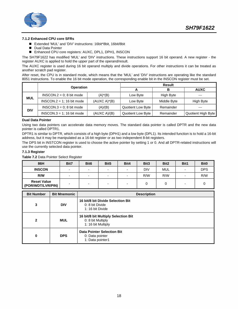
Dual Data Pointer Using two data pointers can accelerate data memory moves. The standard data pointer is called DPTR and the new data pointer is called DPTR1. DPTR1 is similar to DPTR, which consists of a high byte (DPH1) and a low byte (DPL1). Its intended function is to hold a 16-bit address, but it may be manipulated as a 16-bit register or as two independent 8-bit registers. The DPS bit in INSTCON register is used to choose the active pointer by setting 1 or 0. And all DPTR-related instructions will use the currently selected data pointer. 7.1.3 Register Table 7.2 Data Pointer Select Register
86H Bit7 Bit6 Bit5 Bit4 Bit3 Bit2 Bit1 Bit0 INSCON - - - - DIV MUL - DPS
R/W - - - - R/W R/W - R/W
Reset Value (POR/WDT/LVR/PIN) - - - - 0 0 - 0
Bit Number Bit Mnemonic Description
3 DIV 16 bit/8 bit Divide Selection Bit
0: 8 bit Divide 1: 16 bit Divide
2 MUL 16 bit/8 bit Multiply Selection Bit
0: 8 bit Multiply 1: 16 bit Multiply
0 DPS Data Pointer Selection Bit
0: Data pointer 1: Data pointer1
SH79F1622
19
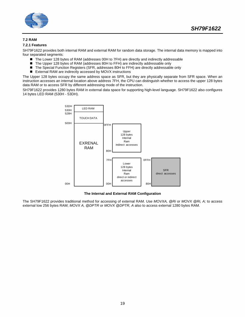
7.2 RAM 7.2.1 Features SH79F1622 provides both internal RAM and external RAM for random data storage. The internal data memory is mapped into four separated segments:
The Lower 128 bytes of RAM (addresses 00H to 7FH) are directly and indirectly addressable The Upper 128 bytes of RAM (addresses 80H to FFH) are indirectly addressable only The Special Function Registers (SFR, addresses 80H to FFH) are directly addressable only External RAM are indirectly accessed by MOVX instructions
The Upper 128 bytes occupy the same address space as SFR, but they are physically separate from SFR space. When an instruction accesses an internal location above address 7FH, the CPU can distinguish whether to access the upper 128 bytes data RAM or to access SFR by different addressing mode of the instruction. SH79F1622 provides 1280 bytes RAM in external data space for supporting high-level language. SH79F1622 also configures 14 bytes LED RAM (530H - 53DH).
7FH
80H
0FFH
00H 00H
Upper128 bytes
InternalRam
indirect accesses
Lower128 bytes
InternalRam
direct or indirectaccesses
500H
SFRdirect accesses
80H
0FFH
EXRENALRAM
LED RAM
TOUCH DATA
528H
53DH530H
The Internal and External RAM Configuration
The SH79F1622 provides traditional method for accessing of external RAM. Use MOVXA, @Ri or MOVX @Ri, A; to access external low 256 bytes RAM; MOVX A, @DPTR or MOVX @DPTR, A also to access external 1280 bytes RAM.
SH79F1622
20
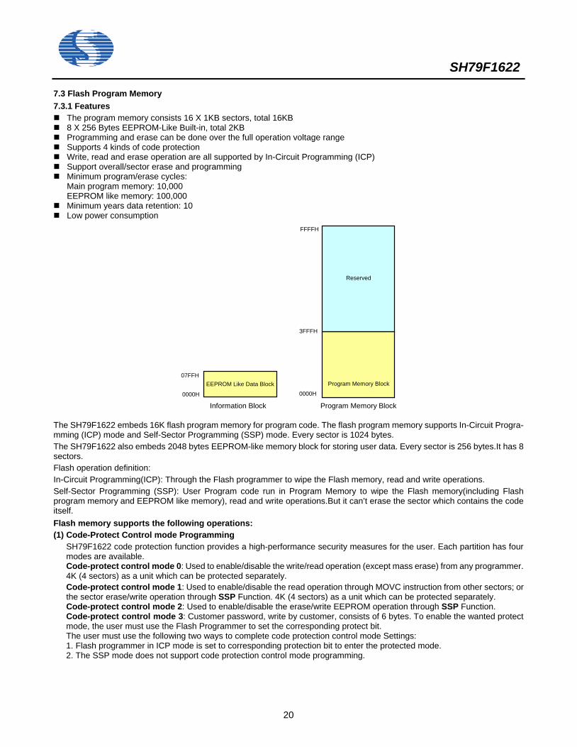
7.3 Flash Program Memory 7.3.1 Features The program memory consists 16 X 1KB sectors, total 16KB 8 X 256 Bytes EEPROM-Like Built-in, total 2KB Programming and erase can be done over the full operation voltage range Supports 4 kinds of code protection Write, read and erase operation are all supported by In-Circuit Programming (ICP) Support overall/sector erase and programming Minimum program/erase cycles:
Main program memory: 10,000 EEPROM like memory: 100,000
Minimum years data retention: 10 Low power consumption
EEPROM Like Data Block Program Memory Block
0000H0000H
Information Block
07FFH
FFFFH
Program Memory Block
Reserved
3FFFH
The SH79F1622 embeds 16K flash program memory for program code. The flash program memory supports In-Circuit Progra- mming (ICP) mode and Self-Sector Programming (SSP) mode. Every sector is 1024 bytes. The SH79F1622 also embeds 2048 bytes EEPROM-like memory block for storing user data. Every sector is 256 bytes.It has 8 sectors. Flash operation definition: In-Circuit Programming(ICP): Through the Flash programmer to wipe the Flash memory, read and write operations. Self-Sector Programming (SSP): User Program code run in Program Memory to wipe the Flash memory(including Flash program memory and EEPROM like memory), read and write operations.But it can’t erase the sector which contains the code itself. Flash memory supports the following operations: (1) Code-Protect Control mode Programming
SH79F1622 code protection function provides a high-performance security measures for the user. Each partition has four modes are available. Code-protect control mode 0: Used to enable/disable the write/read operation (except mass erase) from any programmer. 4K (4 sectors) as a unit which can be protected separately. Code-protect control mode 1: Used to enable/disable the read operation through MOVC instruction from other sectors; or the sector erase/write operation through SSP Function. 4K (4 sectors) as a unit which can be protected separately. Code-protect control mode 2: Used to enable/disable the erase/write EEPROM operation through SSP Function. Code-protect control mode 3: Customer password, write by customer, consists of 6 bytes. To enable the wanted protect mode, the user must use the Flash Programmer to set the corresponding protect bit. The user must use the following two ways to complete code protection control mode Settings: 1. Flash programmer in ICP mode is set to corresponding protection bit to enter the protected mode. 2. The SSP mode does not support code protection control mode programming.
SH79F1622
21
(2) Mass Erase
The mass erase operation will erase all the contents of program code, code option, code protect bit and customer code ID, regardless the status of code-protect control mode. (The Flash Programmer supplies customer code ID setting function for customer to distinguish their product.) Mass erase is only available in Flash Programmer.
(3) Sector Erase The sector erase operation will erase the contents of program code of selected sector. This operation can be done by Flash Programmer or the user’s program. If done by the user’s program, Code-protect control mode 1 and Code-protect control mode 2 of the selected sector must be disabled. If done by the Flash Programmer, Code-protect control mode 0 of the selected sector must be disabled. If Code-protect control mode 3 is enabled, the password must be input correctly. The user must use one of the following two ways to complete sector erasure: 1. Flash programmer in ICP mode send sector erasure instruction to run sector erasure. 2. Through the SSP function send sector erasure instruction to run sector erasure (see chapter SSP)
(4) EEPROM-like Memory Block Erasure EEPROM-like memory block erasure operations will erase the content in EEPROM-like memory block.The user program (SSP) and Flash programmer can perform this operation. The user must use one of the following two ways to complete EEPROM-like memory block erasure: 1. Flash programmer in ICP mode send EEPROM-like memory block erasure instruction to run EEPROM-like memory block
erasure. 2. Through the SSP function send EEPROM-like memory block erasure instruction to run EEPROM-like memory block
erasure (see chapter SSP). (5) Write/Read Code
Write/read code operation can read or write code from flash memory block.The user program (SSP) and Flash programmer can perform this operation. For user programs to perform read operation, code-protect control mode 1 of the selected sector must be forbidden. Regardless of the security bit Settings or not, the user program can read/write the sector which contains program itself (1K/unit). For user programs to perform write operation, code-protect control mode 1 and code-protect control mode 2 of the selected sector must be forbidden. Note: If only use code-protect control mode 1 of the sector, the user programs can’t write other sectors, but it can write the sector which contains program itself (1K/unit). For Flash programmer to perform the operation, code-protect control mode 0 of the selected sector must be forbidden. The user must use one of the following two ways to complete write/read code: 1. Flash programmer in ICP mode send write/read code instruction to write/read code. 2. Through the SSP function send write code instruction to write code; through MOVC instruction to perform read operation.
(6) Write/Read EEPROM-like Memory Block EEPROM-like memory block operation can read or write data from EEPROM-like memory block.The user program (SSP) and Flash programmer can perform this operation. The user must use one of the following two ways to complete write/read EEPROM-like memory block: 1. Flash programmer in ICP mode send write/read EEPROM-like memory block instruction to run write/read EEPROM-like
memory block. 2. Through the SSP function send write/read EEPROM-like memory block instruction to run write/read EEPROM-like
memory block; through MOVC instruction to perform read EEPROM-like operation. Flash Memory Block Operation Summary
Code Protection Support Non Support
Sector erasure Support (no security bit) Support (no security bit)
Overall erasure Support Non support
EEPROM-like memory block erasure Support Support
Write/read code Support (no security bit) Support (no security bit)
Read/write EEPROM-like memory block Support Support
Code protection Support Non support
SH79F1622
22
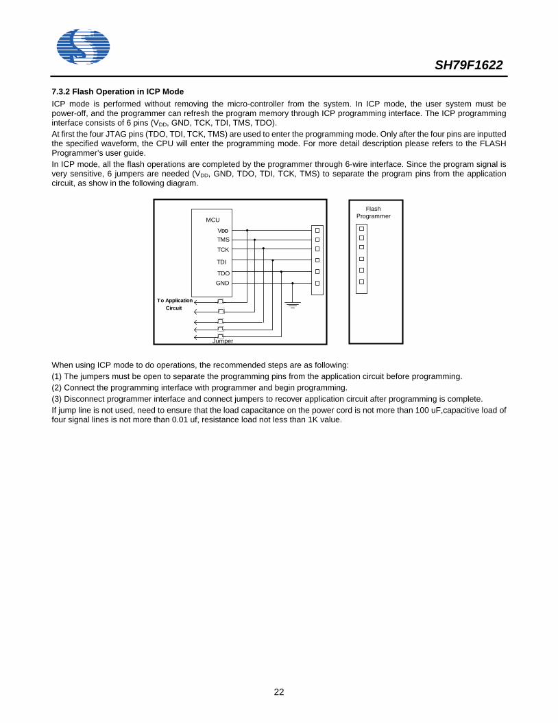
7.3.2 Flash Operation in ICP Mode ICP mode is performed without removing the micro-controller from the system. In ICP mode, the user system must be power-off, and the programmer can refresh the program memory through ICP programming interface. The ICP programming interface consists of 6 pins (VDD, GND, TCK, TDI, TMS, TDO). At first the four JTAG pins (TDO, TDI, TCK, TMS) are used to enter the programming mode. Only after the four pins are inputted the specified waveform, the CPU will enter the programming mode. For more detail description please refers to the FLASH Programmer’s user guide. In ICP mode, all the flash operations are completed by the programmer through 6-wire interface. Since the program signal is very sensitive, 6 jumpers are needed (VDD, GND, TDO, TDI, TCK, TMS) to separate the program pins from the application circuit, as show in the following diagram.
MCU
TCK
TDI
TDOGND
To ApplicationCircuit
Jumper
FlashProgrammer
VDD
TMS
When using ICP mode to do operations, the recommended steps are as following: (1) The jumpers must be open to separate the programming pins from the application circuit before programming. (2) Connect the programming interface with programmer and begin programming. (3) Disconnect programmer interface and connect jumpers to recover application circuit after programming is complete. If jump line is not used, need to ensure that the load capacitance on the power cord is not more than 100 uF,capacitive load of four signal lines is not more than 0.01 uf, resistance load not less than 1K value.
SH79F1622
23
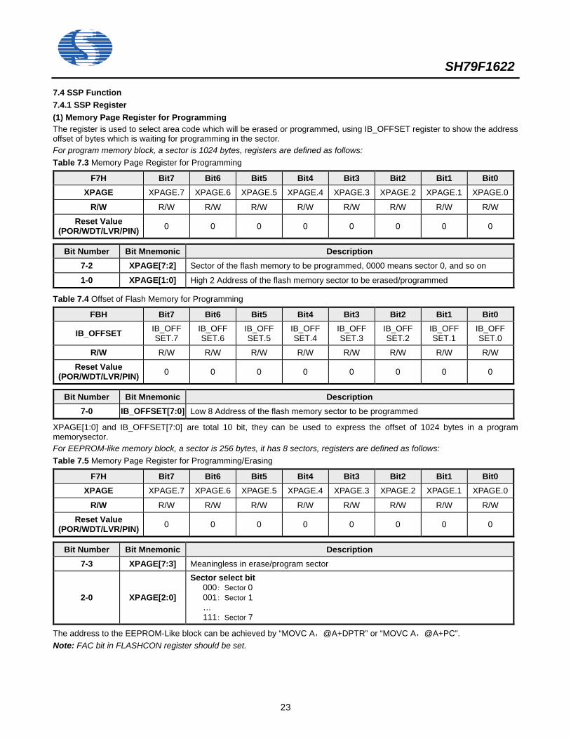
7.4 SSP Function 7.4.1 SSP Register (1) Memory Page Register for Programming The register is used to select area code which will be erased or programmed, using IB_OFFSET register to show the address offset of bytes which is waiting for programming in the sector. For program memory block, a sector is 1024 bytes, registers are defined as follows: Table 7.3 Memory Page Register for Programming
F7H Bit7 Bit6 Bit5 Bit4 Bit3 Bit2 Bit1 Bit0 XPAGE XPAGE.7 XPAGE.6 XPAGE.5 XPAGE.4 XPAGE.3 XPAGE.2 XPAGE.1 XPAGE.0
R/W R/W R/W R/W R/W R/W R/W R/W R/W
Reset Value (POR/WDT/LVR/PIN) 0 0 0 0 0 0 0 0
Bit Number Bit Mnemonic Description 7-2 XPAGE[7:2] Sector of the flash memory to be programmed, 0000 means sector 0, and so on
1-0 XPAGE[1:0] High 2 Address of the flash memory sector to be erased/programmed
Table 7.4 Offset of Flash Memory for Programming
FBH Bit7 Bit6 Bit5 Bit4 Bit3 Bit2 Bit1 Bit0
IB_OFFSET IB_OFF SET.7
IB_OFF SET.6
IB_OFF SET.5
IB_OFF SET.4
IB_OFF SET.3
IB_OFF SET.2
IB_OFF SET.1
IB_OFF SET.0
R/W R/W R/W R/W R/W R/W R/W R/W R/W
Reset Value (POR/WDT/LVR/PIN) 0 0 0 0 0 0 0 0
Bit Number Bit Mnemonic Description 7-0 IB_OFFSET[7:0] Low 8 Address of the flash memory sector to be programmed
XPAGE[1:0] and IB_OFFSET[7:0] are total 10 bit, they can be used to express the offset of 1024 bytes in a program memorysector. For EEPROM-like memory block, a sector is 256 bytes, it has 8 sectors, registers are defined as follows: Table 7.5 Memory Page Register for Programming/Erasing
F7H Bit7 Bit6 Bit5 Bit4 Bit3 Bit2 Bit1 Bit0 XPAGE XPAGE.7 XPAGE.6 XPAGE.5 XPAGE.4 XPAGE.3 XPAGE.2 XPAGE.1 XPAGE.0
R/W R/W R/W R/W R/W R/W R/W R/W R/W
Reset Value (POR/WDT/LVR/PIN) 0 0 0 0 0 0 0 0
Bit Number Bit Mnemonic Description 7-3 XPAGE[7:3] Meaningless in erase/program sector
2-0 XPAGE[2:0]
Sector select bit 000: Sector 0 001: Sector 1 … 111: Sector 7
The address to the EEPROM-Like block can be achieved by “MOVC A,@A+DPTR” or “MOVC A,@A+PC”. Note: FAC bit in FLASHCON register should be set.
SH79F1622
24
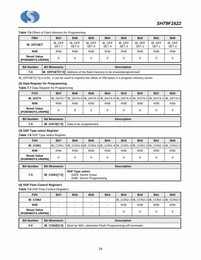
Table 7.6 Offset of Flash Memory for Programming
FBH Bit7 Bit6 Bit5 Bit4 Bit3 Bit2 Bit1 Bit0
IB_OFFSET IB_OFF SET.7
IB_OFF SET.6
IB_OFF SET.5
IB_OFF SET.4
IB_OFF SET.3
IB_OFF SET.2
IB_OFF SET.1
IB_OFF SET.0
R/W R/W R/W R/W R/W R/W R/W R/W R/W
Reset Value (POR/WDT/LVR/PIN) 0 0 0 0 0 0 0 0
Bit Number Bit Mnemonic Description 7-0 IB_OFFSET[7:0] Address of the flash memory to be erased/programmed
IB_OFFSET[7:0] is 8 bit, it can be used to express the offset of 256 bytes in a program memory sector.
(2) Data Register for Programming Table 7.7 Data Register for Programming
FCH Bit7 Bit6 Bit5 Bit4 Bit3 Bit2 Bit1 Bit0 IB_DATA IB_DATA.7 IB_DATA.6 IB_DATA.5 IB_DATA.4 IB_DATA.3 IB_DATA.2 IB_DATA.1 IB_DATA.0
R/W R/W R/W R/W R/W R/W R/W R/W R/W
Reset Value (POR/WDT/LVR/PIN) 0 0 0 0 0 0 0 0
Bit Number Bit Mnemonic Description 7-0 IB_DATA[7:0] Data to be programmed
(3) SSP Type select Register Table 7.8 SSP Type select Register
F2H Bit7 Bit6 Bit5 Bit4 Bit3 Bit2 Bit1 Bit0 IB_CON1 IB_CON1.7 IB_CON1.6 IB_CON1.5 IB_CON1.4 IB_CON1.3 IB_CON1.2 IB_CON1.1 IB_CON1.0
R/W R/W R/W R/W R/W R/W R/W R/W R/W
Reset Value (POR/WDT/LVR/PIN) 0 0 0 0 0 0 0 0
Bit Number Bit Mnemonic Description
7-0 IB_CON1[7:0] SSP Type select
0xE6: Sector Erase 0x6E: Sector Programming
(4) SSP Flow Control Register1 Table 7.9 SSP Flow Control Register1
F3H Bit7 Bit6 Bit5 Bit4 Bit3 Bit2 Bit1 Bit0 IB_CON2 - - - - IB_CON2.3 IB_CON2.2 IB_CON2.1 IB_CON2.0
R/W - - - - R/W R/W R/W R/W
Reset Value (POR/WDT/LVR/PIN) - - - - 0 0 0 0
Bit Number Bit Mnemonic Description 3-0 IB_CON2[3:0] Must be 05H, otherwise Flash Programming will terminate
SH79F1622
25
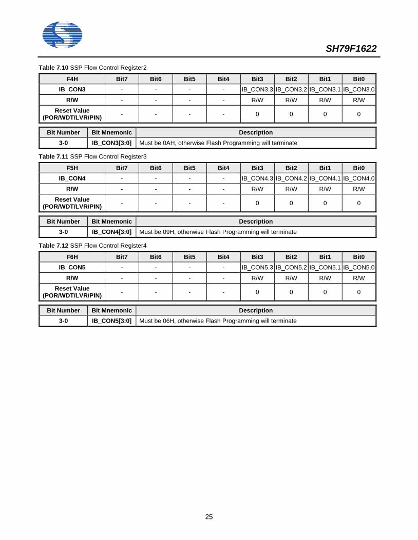
Table 7.10 SSP Flow Control Register2
F4H Bit7 Bit6 Bit5 Bit4 Bit3 Bit2 Bit1 Bit0 IB_CON3 - - - - IB_CON3.3 IB_CON3.2 IB_CON3.1 IB_CON3.0
R/W - - - - R/W R/W R/W R/W
Reset Value (POR/WDT/LVR/PIN) - - - - 0 0 0 0
Bit Number Bit Mnemonic Description 3-0 IB_CON3[3:0] Must be 0AH, otherwise Flash Programming will terminate
Table 7.11 SSP Flow Control Register3
F5H Bit7 Bit6 Bit5 Bit4 Bit3 Bit2 Bit1 Bit0 IB_CON4 - - - - IB_CON4.3 IB_CON4.2 IB_CON4.1 IB_CON4.0
R/W - - - - R/W R/W R/W R/W
Reset Value (POR/WDT/LVR/PIN) - - - - 0 0 0 0
Bit Number Bit Mnemonic Description 3-0 IB_CON4[3:0] Must be 09H, otherwise Flash Programming will terminate
Table 7.12 SSP Flow Control Register4
F6H Bit7 Bit6 Bit5 Bit4 Bit3 Bit2 Bit1 Bit0 IB_CON5 - - - - IB_CON5.3 IB_CON5.2 IB_CON5.1 IB_CON5.0
R/W - - - - R/W R/W R/W R/W
Reset Value (POR/WDT/LVR/PIN) - - - - 0 0 0 0
Bit Number Bit Mnemonic Description 3-0 IB_CON5[3:0] Must be 06H, otherwise Flash Programming will terminate
SH79F1622
26
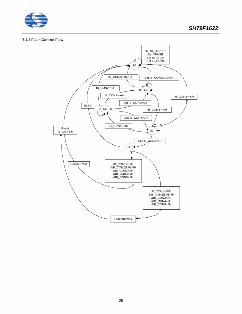
7.4.2 Flash Control Flow
S0
S1
S2
S3
S4
IB_CON1=E6H&IB_CON2[3:0]=5H
&IB_CON3=AH&IB_CON4=9H&IB_CON5=6H
IB_CON1=6EH&IB_CON2[3:0]=5H
&IB_CON3=AH&IB_CON4=9H&IB_CON5=6H
Programming
Set IB_OFFSETSet XPAGE
Set IB_DATASet IB_CON1
IB_CON2≠5H
IB_CON2[3:0]≠5H Set IB_CON2[3:0]=5H
IB_CON3≠AH
Set IB_CON3=AH
IB_CON3≠AH
Set IB_CON4=9H
IB_CON4≠9H
Set IB_CON5=6H
IB_CON2≠5H
ELSE
Sector Erase
ResetIB_CON1-5
SH79F1622
27
7.4.3 SSP Programming Notice To successfully complete SSP programming, the user’s software must be set as the following the steps: (1) For Code/Data Programming: Note: must close Code-protect control mode 1 and Code-protect control mode 2.
1. Disable interrupt; 2. Fill in the XPAGE, IB_OFFSET for the corresponding address; 3. Fill in IB_DATA, if programming is wanted; 4. Fill in IB_CON1-5 sequentially; 5. Add 4 nops for more stable operation; 6. Code/Data programming, CPU will be in IDLE mode; 7. Go to Step 2, if more data are to be programmed; 8. Clear XPAGE; enable interrupt if necessary.
(2) For Sector Erase: Note: must close Code-protect control mode 1 and Code-protect control mode 2. 1. Disable interrupt; 2. Fill in the XPAGE for the corresponding sector; 3. Fill in IB_CON1-5 sequentially; 4. Add 4 NOPs for more stable operation; 5. Sector Erase, CPU will be in IDLE mode; 6. Go to step 2, if more sectors are to be erased; 7. Clear XPAGE; enable interrupt if necessary.
(3) For Code Reading: Just Use “MOVC A, @A+DPTR” or “MOVC A, @A+PC”.
(4) For EEPROM-Like: Note: The function is not controlled by code protect control mode. The operation for EEPROM-Like is similar to the operation for Flash memory, the differences are: 1. FAC bit in FLASHCON register must be set before wipe, read or write EEPROM-Like. 2. EEPROM-Like sector is 256 bytes, rather than 1024 bytes. Note: FAC bit must be cleared when do not operate EEPROM-Like.
7.4.4 Readable Random Code Every chip is cured an 24-bit readable random code after production. Readable random code is 0 - 0xffffff random value, and can not be erased, can be read by program or tools. How to read random code: set FAC bit, Assigned to the DPTR as “0127DH - 127FH”, clear A, then use “MOVC A, @A+DPTR” to read. Note: It is needed to clear FAC after reading readable random code, otherwise it will influence on the instructions execution of reading program ROM. FLASHCON register description is as follows:
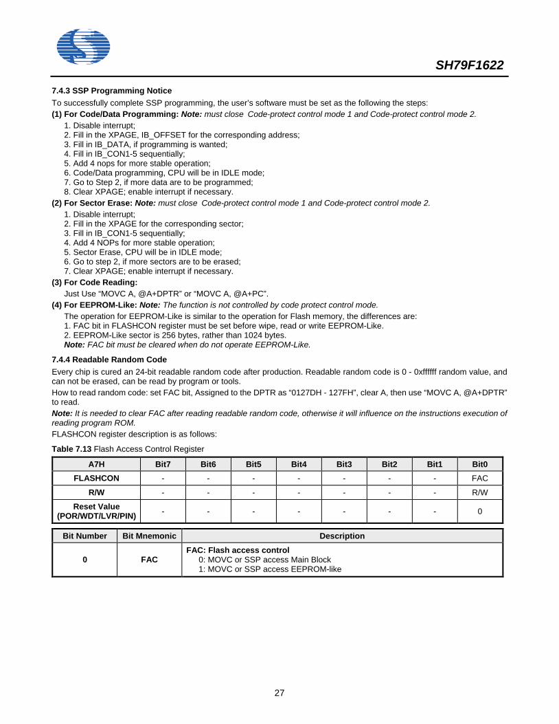
Table 7.13 Flash Access Control Register
A7H Bit7 Bit6 Bit5 Bit4 Bit3 Bit2 Bit1 Bit0 FLASHCON - - - - - - - FAC
R/W - - - - - - - R/W
Reset Value (POR/WDT/LVR/PIN) - - - - - - - 0
Bit Number Bit Mnemonic Description
0 FAC FAC: Flash access control
0: MOVC or SSP access Main Block 1: MOVC or SSP access EEPROM-like
SH79F1622
28
7.5 System Clock and Oscillator 7.5.1 Features 2 oscillator types: 32.768kHz crystal, 27MHz internal RC Built-in 27MHz (±1%) internal RC (at normal temperature) Built-in 32.768kHz speed up circuit Built-in system clock prescaler
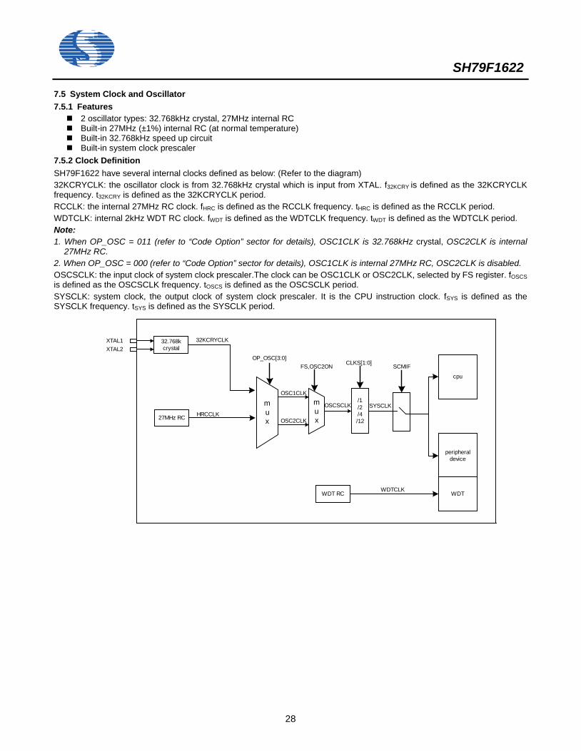
7.5.2 Clock Definition SH79F1622 have several internal clocks defined as below: (Refer to the diagram) 32KCRYCLK: the oscillator clock is from 32.768kHz crystal which is input from XTAL. f32KCRY is defined as the 32KCRYCLK frequency. t32KCRY is defined as the 32KCRYCLK period. RCCLK: the internal 27MHz RC clock. fHRC is defined as the RCCLK frequency. tHRC is defined as the RCCLK period. WDTCLK: internal 2kHz WDT RC clock. fWDT is defined as the WDTCLK frequency. tWDT is defined as the WDTCLK period. Note: 1. When OP_OSC = 011 (refer to “Code Option” sector for details), OSC1CLK is 32.768kHz crystal, OSC2CLK is internal
27MHz RC. 2. When OP_OSC = 000 (refer to “Code Option” sector for details), OSC1CLK is internal 27MHz RC, OSC2CLK is disabled. OSCSCLK: the input clock of system clock prescaler.The clock can be OSC1CLK or OSC2CLK, selected by FS register. fOSCS is defined as the OSCSCLK frequency. tOSCS is defined as the OSCSCLK period. SYSCLK: system clock, the output clock of system clock prescaler. It is the CPU instruction clock. fSYS is defined as the SYSCLK frequency. tSYS is defined as the SYSCLK period.
32.768kcrystal
27MHz RC
WDT RC
mux
mux
/1/2/4/12
cpu
peripheraldevice
SYSCLKOSCSCLK
OSC1CLK
OSC2CLK
32KCRYCLK
HRCCLK
WDTWDTCLK
OP_OSC[3:0]FS,OSC2ON CLKS[1:0] SCMIF
XTAL1XTAL2
SH79F1622
29
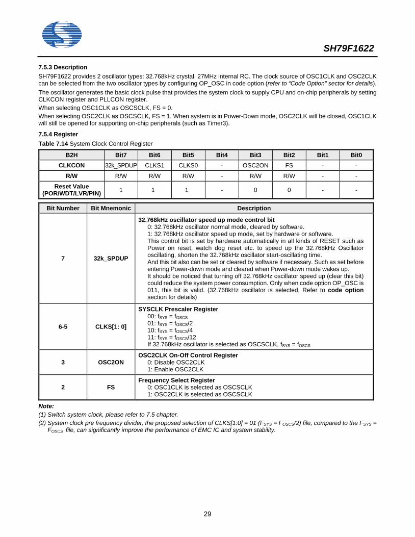
7.5.3 Description SH79F1622 provides 2 oscillator types: 32.768kHz crystal, 27MHz internal RC. The clock source of OSC1CLK and OSC2CLK can be selected from the two oscillator types by configuring OP_OSC in code option (refer to “Code Option” sector for details). The oscillator generates the basic clock pulse that provides the system clock to supply CPU and on-chip peripherals by setting CLKCON register and PLLCON register. When selecting OSC1CLK as OSCSCLK, FS = 0. When selecting OSC2CLK as OSCSCLK, FS = 1. When system is in Power-Down mode, OSC2CLK will be closed, OSC1CLK will still be opened for supporting on-chip peripherals (such as Timer3).
7.5.4 Register Table 7.14 System Clock Control Register
B2H Bit7 Bit6 Bit5 Bit4 Bit3 Bit2 Bit1 Bit0 CLKCON 32k_SPDUP CLKS1 CLKS0 - OSC2ON FS - -
R/W R/W R/W R/W - R/W R/W - -
Reset Value (POR/WDT/LVR/PIN) 1 1 1 - 0 0 - -
Bit Number Bit Mnemonic Description
7 32k_SPDUP
32.768kHz oscillator speed up mode control bit 0: 32.768kHz oscillator normal mode, cleared by software. 1: 32.768kHz oscillator speed up mode, set by hardware or software. This control bit is set by hardware automatically in all kinds of RESET such as Power on reset, watch dog reset etc. to speed up the 32.768kHz Oscillator oscillating, shorten the 32.768kHz oscillator start-oscillating time. And this bit also can be set or cleared by software if necessary. Such as set before entering Power-down mode and cleared when Power-down mode wakes up. It should be noticed that turning off 32.768kHz oscillator speed up (clear this bit) could reduce the system power consumption. Only when code option OP_OSC is 011, this bit is valid. (32.768kHz oscillator is selected, Refer to code option section for details)
6-5 CLKS[1: 0]
SYSCLK Prescaler Register 00: fSYS = fOSCS 01: fSYS = fOSCS/2 10: fSYS = fOSCS/4 11: fSYS = fOSCS/12 If 32.768kHz oscillator is selected as OSCSCLK, fSYS = fOSCS
3 OSC2ON OSC2CLK On-Off Control Register
0: Disable OSC2CLK 1: Enable OSC2CLK
2 FS Frequency Select Register
0: OSC1CLK is selected as OSCSCLK 1: OSC2CLK is selected as OSCSCLK
Note: (1) Switch system clock, please refer to 7.5 chapter. (2) System clock pre frequency divider, the proposed selection of CLKS[1:0] = 01 (FSYS = FOSCS/2) file, compared to the FSYS =
FOSCS file, can significantly improve the performance of EMC IC and system stability.
SH79F1622
30
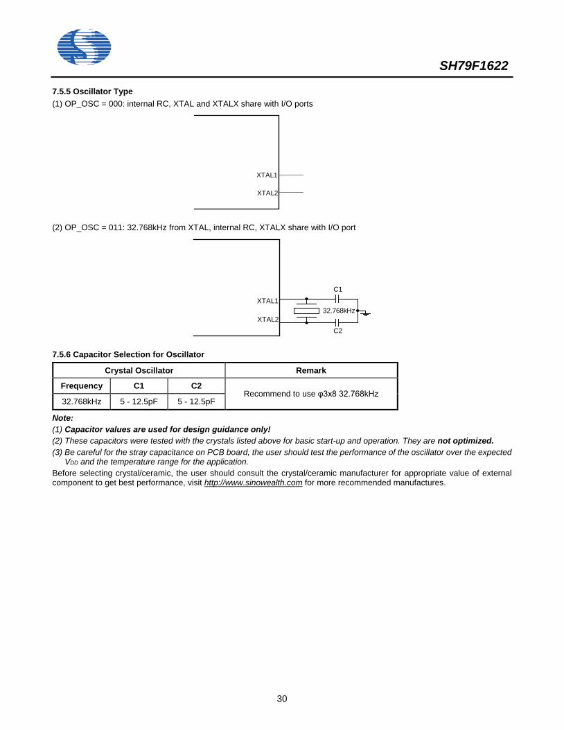
7.5.5 Oscillator Type (1) OP_OSC = 000: internal RC, XTAL and XTALX share with I/O ports
XTAL1
XTAL2
(2) OP_OSC = 011: 32.768kHz from XTAL, internal RC, XTALX share with I/O port
XTAL1
XTAL2
C1
C2
32.768kHz
7.5.6 Capacitor Selection for Oscillator
Crystal Oscillator Remark
Frequency C1 C2 Recommend to use φ3x8 32.768kHz
32.768kHz 5 - 12.5pF 5 - 12.5pF
Note: (1) Capacitor values are used for design guidance only! (2) These capacitors were tested with the crystals listed above for basic start-up and operation. They are not optimized. (3) Be careful for the stray capacitance on PCB board, the user should test the performance of the oscillator over the expected
VDD and the temperature range for the application. Before selecting crystal/ceramic, the user should consult the crystal/ceramic manufacturer for appropriate value of external component to get best performance, visit http://www.sinowealth.com for more recommended manufactures.
SH79F1622
31
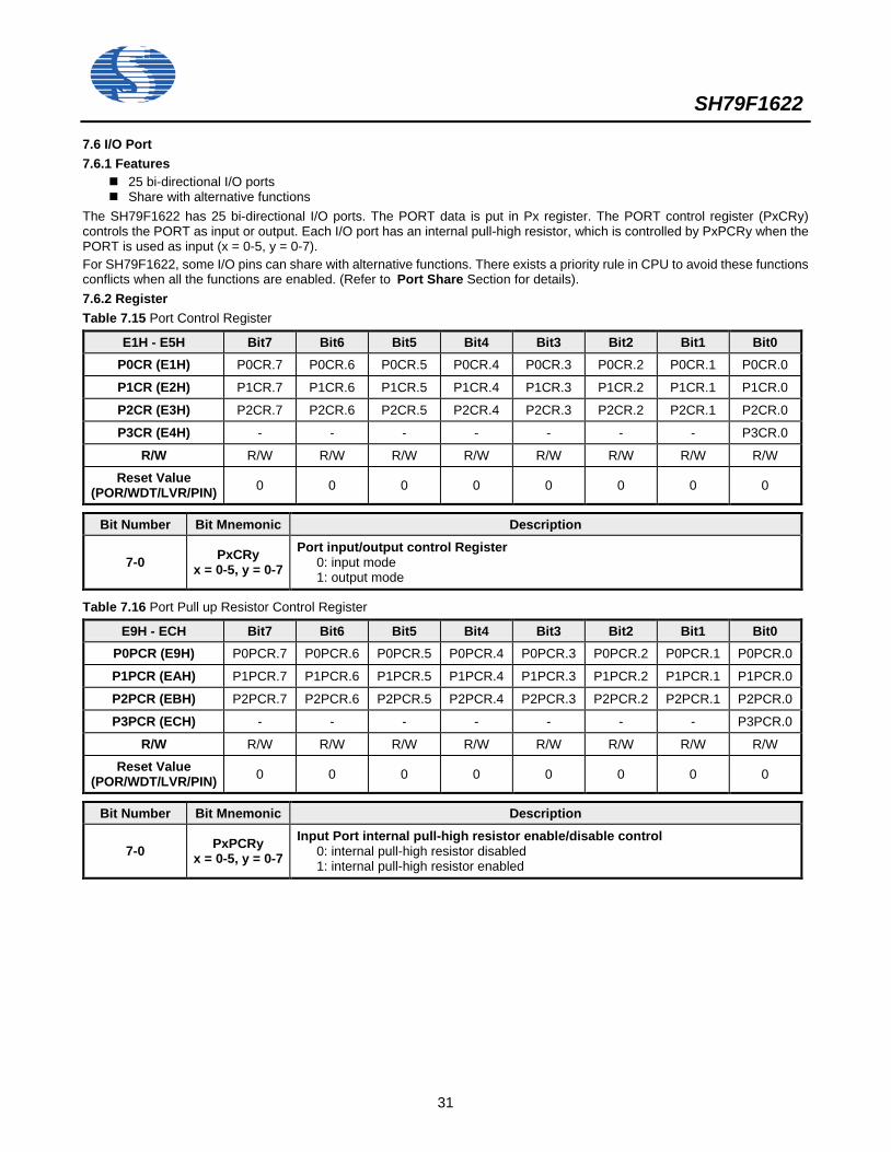
7.6 I/O Port 7.6.1 Features
25 bi-directional I/O ports Share with alternative functions
The SH79F1622 has 25 bi-directional I/O ports. The PORT data is put in Px register. The PORT control register (PxCRy) controls the PORT as input or output. Each I/O port has an internal pull-high resistor, which is controlled by PxPCRy when the PORT is used as input (x = 0-5, y = 0-7). For SH79F1622, some I/O pins can share with alternative functions. There exists a priority rule in CPU to avoid these functions conflicts when all the functions are enabled. (Refer to Port Share Section for details). 7.6.2 Register Table 7.15 Port Control Register
E1H - E5H Bit7 Bit6 Bit5 Bit4 Bit3 Bit2 Bit1 Bit0 P0CR (E1H) P0CR.7 P0CR.6 P0CR.5 P0CR.4 P0CR.3 P0CR.2 P0CR.1 P0CR.0
P1CR (E2H) P1CR.7 P1CR.6 P1CR.5 P1CR.4 P1CR.3 P1CR.2 P1CR.1 P1CR.0
P2CR (E3H) P2CR.7 P2CR.6 P2CR.5 P2CR.4 P2CR.3 P2CR.2 P2CR.1 P2CR.0
P3CR (E4H) - - - - - - - P3CR.0
R/W R/W R/W R/W R/W R/W R/W R/W R/W
Reset Value (POR/WDT/LVR/PIN) 0 0 0 0 0 0 0 0
Bit Number Bit Mnemonic Description
7-0 PxCRy x = 0-5, y = 0-7
Port input/output control Register 0: input mode 1: output mode
Table 7.16 Port Pull up Resistor Control Register
E9H - ECH Bit7 Bit6 Bit5 Bit4 Bit3 Bit2 Bit1 Bit0 P0PCR (E9H) P0PCR.7 P0PCR.6 P0PCR.5 P0PCR.4 P0PCR.3 P0PCR.2 P0PCR.1 P0PCR.0
P1PCR (EAH) P1PCR.7 P1PCR.6 P1PCR.5 P1PCR.4 P1PCR.3 P1PCR.2 P1PCR.1 P1PCR.0
P2PCR (EBH) P2PCR.7 P2PCR.6 P2PCR.5 P2PCR.4 P2PCR.3 P2PCR.2 P2PCR.1 P2PCR.0
P3PCR (ECH) - - - - - - - P3PCR.0
R/W R/W R/W R/W R/W R/W R/W R/W R/W
Reset Value (POR/WDT/LVR/PIN) 0 0 0 0 0 0 0 0
Bit Number Bit Mnemonic Description
7-0 PxPCRy x = 0-5, y = 0-7
Input Port internal pull-high resistor enable/disable control 0: internal pull-high resistor disabled 1: internal pull-high resistor enabled
SH79F1622
32
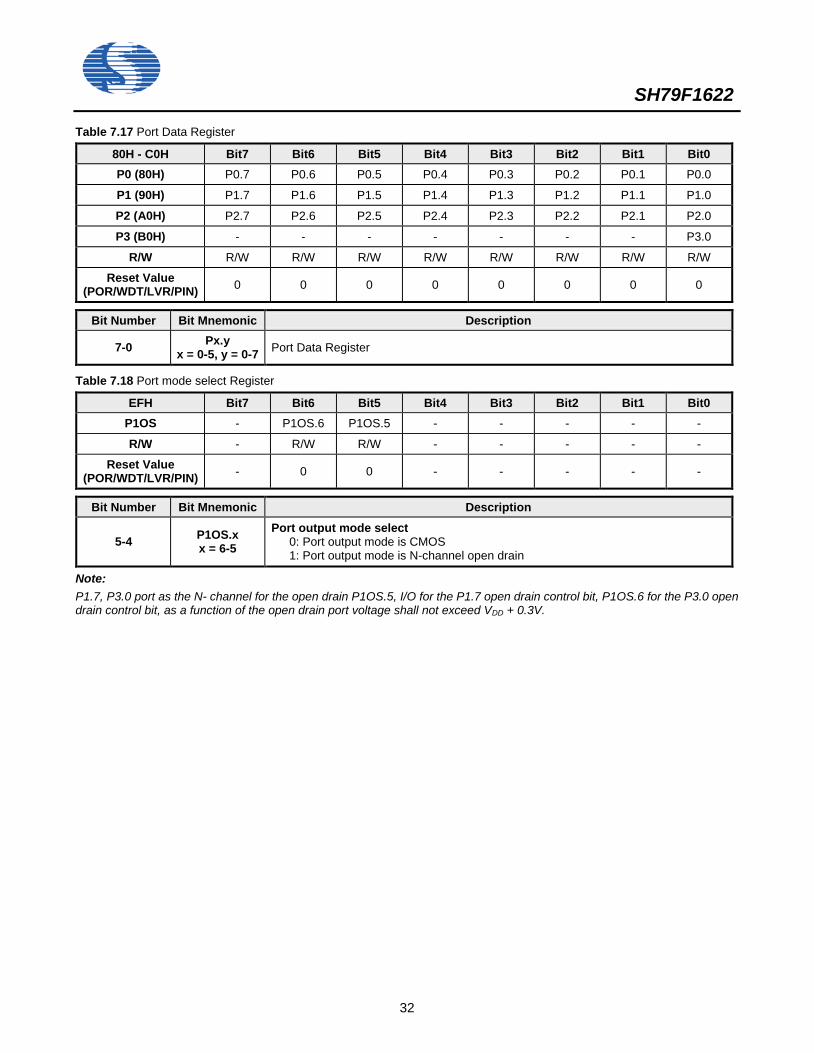
Table 7.17 Port Data Register
80H - C0H Bit7 Bit6 Bit5 Bit4 Bit3 Bit2 Bit1 Bit0 P0 (80H) P0.7 P0.6 P0.5 P0.4 P0.3 P0.2 P0.1 P0.0
P1 (90H) P1.7 P1.6 P1.5 P1.4 P1.3 P1.2 P1.1 P1.0
P2 (A0H) P2.7 P2.6 P2.5 P2.4 P2.3 P2.2 P2.1 P2.0
P3 (B0H) - - - - - - - P3.0
R/W R/W R/W R/W R/W R/W R/W R/W R/W
Reset Value (POR/WDT/LVR/PIN) 0 0 0 0 0 0 0 0
Bit Number Bit Mnemonic Description
7-0 Px.y x = 0-5, y = 0-7 Port Data Register
Table 7.18 Port mode select Register
EFH Bit7 Bit6 Bit5 Bit4 Bit3 Bit2 Bit1 Bit0 P1OS - P1OS.6 P1OS.5 - - - - -
R/W - R/W R/W - - - - -
Reset Value (POR/WDT/LVR/PIN) - 0 0 - - - - -
Bit Number Bit Mnemonic Description
5-4 P1OS.x x = 6-5
Port output mode select 0: Port output mode is CMOS 1: Port output mode is N-channel open drain
Note: P1.7, P3.0 port as the N- channel for the open drain P1OS.5, I/O for the P1.7 open drain control bit, P1OS.6 for the P3.0 open drain control bit, as a function of the open drain port voltage shall not exceed VDD + 0.3V.
SH79F1622
33
7.6.3 Port Diagram
DataRegister
Data Bus
Write
Read Port Pad
PxCRy
Read Data Register/Pad SelectionRead
PxPCRy Output Mode
I/O Pad
0: From Pad1: From data register
SFEN
SecondFunction
Input Mode
Read Port Data Register
(Pull-up) 0 = ON1 = OFF
VDD VDD
0 = OFF1 = ON
Note: (1) The input source of reading input port operation is from the input pin directly. (2) The input source of reading output port operation has two paths, one is from the port data Register, and the other is from the
output pin directly. The read Instruction distinguishes which path is selected: The read-modify-write instruction is for the reading of the data register in output mode, and the other instructions are for reading of the output pin directly.
(3) The destination of writing port operation is the data register regardless the port shared as the second function or not. 7.6.4 Port Share The 25 bi-directional I/O ports can also share second or third special function. But the share priority should obey the Outer Most Inner Lest rule: The out most pin function in Pin Configuration has the highest priority, and the inner most pin function has the lowest priority. This means when one pin is occupied by a higher priority function (if enabled), it cannot be used as the lower priority functional pin, even the lower priority function is also enabled. Only until the higher priority function is closed by hardware or software, can the corresponding pin be released for the lower priority function use. Also the function that need pull up resister is also controlled by the same rule. When port share function is enabled, the user can modify PxCR, PxPCR (x = 0-5), but these operations will have no effect on the port status until the second function was disabled. When port share function is enabled, any read or write operation to port will only affect the data register while the port pin keeps unchanged until all the share functions are disabled. PORT0: - TK1-8: Touch Key channel 1-8 (P0.0-O0.7) - SEG0-SEG7: LED SEG 0-7 display output Table 7.19 PORT0 Share Table
Pin No. Priority Function Enable bit
1-4 25-28
1 Tk1-TK8 Set P0SS.0-P0SS.7 bit in P0SS register
2 SEG0-SEG7 Set SEG0-SEG7 bit in SEG01 register
3 P0.0-0.7 Above condition is not met
SH79F1622
34
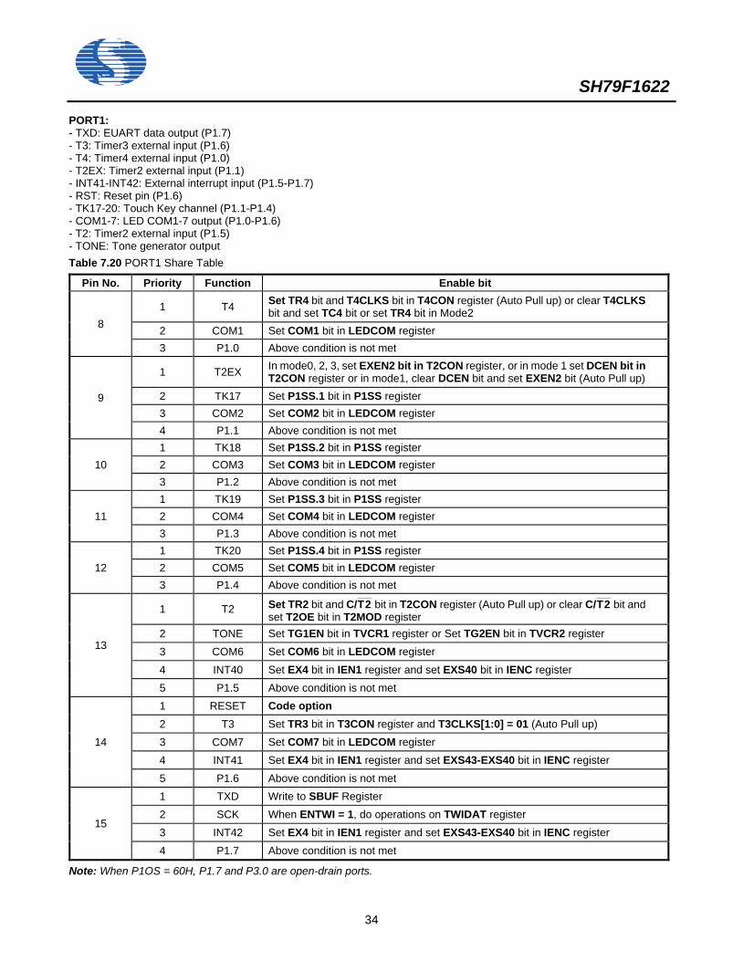
PORT1: - TXD: EUART data output (P1.7) - T3: Timer3 external input (P1.6) - T4: Timer4 external input (P1.0) - T2EX: Timer2 external input (P1.1) - INT41-INT42: External interrupt input (P1.5-P1.7) - RST: Reset pin (P1.6) - TK17-20: Touch Key channel (P1.1-P1.4) - COM1-7: LED COM1-7 output (P1.0-P1.6) - T2: Timer2 external input (P1.5) - TONE: Tone generator output Table 7.20 PORT1 Share Table
Pin No. Priority Function Enable bit
8 1 T4 Set TR4 bit and T4CLKS bit in T4CON register (Auto Pull up) or clear T4CLKS
bit and set TC4 bit or set TR4 bit in Mode2 2 COM1 Set COM1 bit in LEDCOM register 3 P1.0 Above condition is not met
9
1 T2EX In mode0, 2, 3, set EXEN2 bit in T2CON register, or in mode 1 set DCEN bit in T2CON register or in mode1, clear DCEN bit and set EXEN2 bit (Auto Pull up)
2 TK17 Set P1SS.1 bit in P1SS register 3 COM2 Set COM2 bit in LEDCOM register 4 P1.1 Above condition is not met
10 1 TK18 Set P1SS.2 bit in P1SS register 2 COM3 Set COM3 bit in LEDCOM register 3 P1.2 Above condition is not met
11 1 TK19 Set P1SS.3 bit in P1SS register 2 COM4 Set COM4 bit in LEDCOM register 3 P1.3 Above condition is not met
12 1 TK20 Set P1SS.4 bit in P1SS register 2 COM5 Set COM5 bit in LEDCOM register 3 P1.4 Above condition is not met
13
1 T2 Set TR2 bit and C/T----
2----
bit in T2CON register (Auto Pull up) or clear C/T----
2----
bit and set T2OE bit in T2MOD register
2 TONE Set TG1EN bit in TVCR1 register or Set TG2EN bit in TVCR2 register 3 COM6 Set COM6 bit in LEDCOM register 4 INT40 Set EX4 bit in IEN1 register and set EXS40 bit in IENC register 5 P1.5 Above condition is not met
14
1 RESET Code option 2 T3 Set TR3 bit in T3CON register and T3CLKS[1:0] = 01 (Auto Pull up) 3 COM7 Set COM7 bit in LEDCOM register 4 INT41 Set EX4 bit in IEN1 register and set EXS43-EXS40 bit in IENC register
5 P1.6 Above condition is not met
15
1 TXD Write to SBUF Register 2 SCK When ENTWI = 1, do operations on TWIDAT register
3 INT42 Set EX4 bit in IEN1 register and set EXS43-EXS40 bit in IENC register 4 P1.7 Above condition is not met
Note: When P1OS = 60H, P1.7 and P3.0 are open-drain ports.
SH79F1622
35
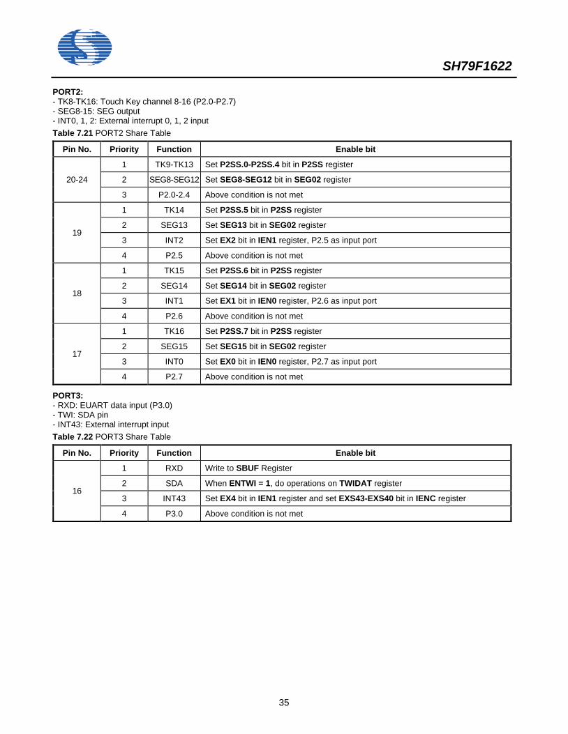
PORT2: - TK8-TK16: Touch Key channel 8-16 (P2.0-P2.7) - SEG8-15: SEG output - INT0, 1, 2: External interrupt 0, 1, 2 input Table 7.21 PORT2 Share Table
Pin No. Priority Function Enable bit
20-24
1 TK9-TK13 Set P2SS.0-P2SS.4 bit in P2SS register
2 SEG8-SEG12 Set SEG8-SEG12 bit in SEG02 register
3 P2.0-2.4 Above condition is not met
19
1 TK14 Set P2SS.5 bit in P2SS register
2 SEG13 Set SEG13 bit in SEG02 register
3 INT2 Set EX2 bit in IEN1 register, P2.5 as input port
4 P2.5 Above condition is not met
18
1 TK15 Set P2SS.6 bit in P2SS register
2 SEG14 Set SEG14 bit in SEG02 register
3 INT1 Set EX1 bit in IEN0 register, P2.6 as input port
4 P2.6 Above condition is not met
17
1 TK16 Set P2SS.7 bit in P2SS register
2 SEG15 Set SEG15 bit in SEG02 register
3 INT0 Set EX0 bit in IEN0 register, P2.7 as input port
4 P2.7 Above condition is not met
PORT3: - RXD: EUART data input (P3.0) - TWI: SDA pin - INT43: External interrupt input Table 7.22 PORT3 Share Table
Pin No. Priority Function Enable bit
16
1 RXD Write to SBUF Register
2 SDA When ENTWI = 1, do operations on TWIDAT register
3 INT43 Set EX4 bit in IEN1 register and set EXS43-EXS40 bit in IENC register
4 P3.0 Above condition is not met
SH79F1622
36
7.7 Timer 7.7.1 Features
The SH79F1622 has three timers (Timer2, 3, 4) Timer2 is compatible with the standard 8052 and has up or down counting and programmable clock output function Timer3 is a 16-bit auto-reload timer and can operate even in Power-Down mode Timer4 is a 16-bit auto-reload timer, two data register: TH4 & TL4 can be used as a 16-bit register to access
7.7.2 Timer2 The Timer 2 is implemented as a 16-bit register accessed as two cascaded data registers: TH2 and TL2. It is controlled by the register T2CON and T2MOD. The Timer2 interrupt can be enabled by setting the ET2 bit in the IEN0 register. (Refer to Interrupt Section for details) C/T2
———
selects system clock (timer operation) or external pin T2 (counter operation) as the timer clock input. Setting TR2 allows Timer 2/Counter 2 Data Register to increment by the selected input. Timer2 Modes Timer2 has 3 operating modes: Capture/Reload, Auto-reload mode with up or down counter and Programmable clock-output. These modes are selected by the combination of CP/RL2. Table 7.23 Timer2 Mode select
C/T2———
T2OE DCEN TR2 CP/RL2 Mode
X 0 X 1 1 0 16 bit capture X 0 0 1 0
1 16 bit auto-reload timer X 0 1 1 0 0 1 X 1 X 2 Programmable clock-output only 1 1 X 1 X Not recommending X X X 0 X X Timer2 stop, the T2EX path still enable
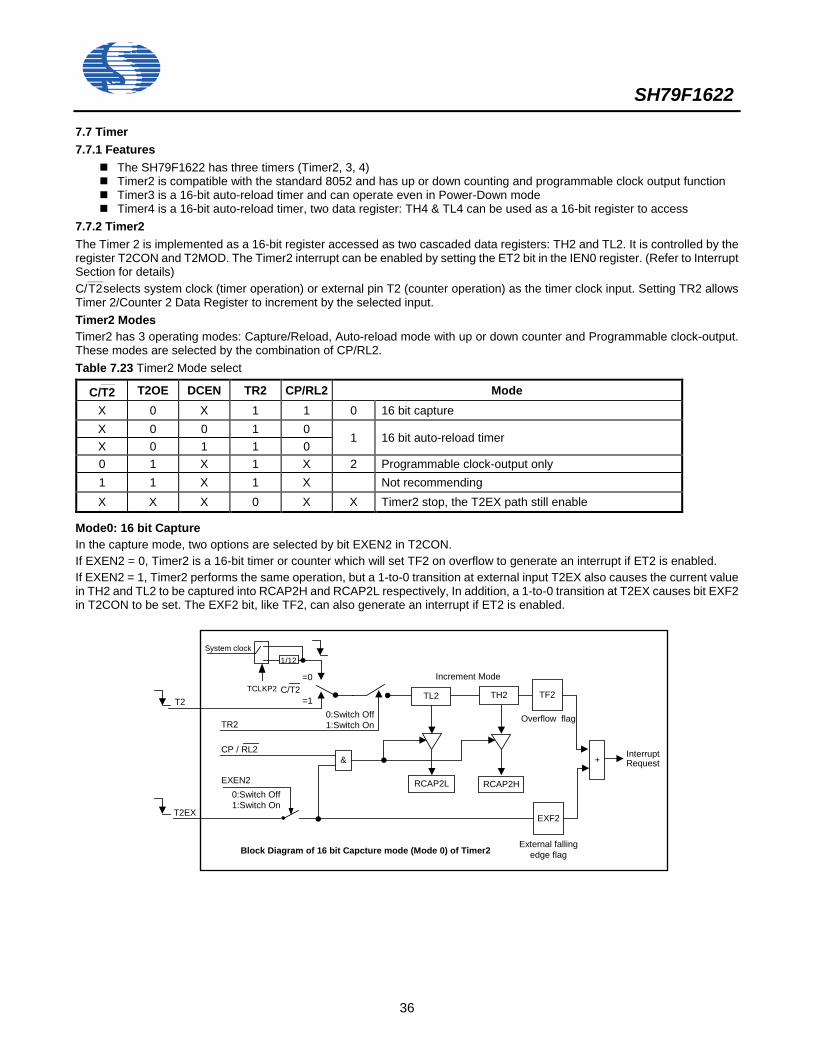
Mode0: 16 bit Capture In the capture mode, two options are selected by bit EXEN2 in T2CON. If EXEN2 = 0, Timer2 is a 16-bit timer or counter which will set TF2 on overflow to generate an interrupt if ET2 is enabled. If EXEN2 = 1, Timer2 performs the same operation, but a 1-to-0 transition at external input T2EX also causes the current value in TH2 and TL2 to be captured into RCAP2H and RCAP2L respectively, In addition, a 1-to-0 transition at T2EX causes bit EXF2 in T2CON to be set. The EXF2 bit, like TF2, can also generate an interrupt if ET2 is enabled.
0:Switch Off1:Switch On
Block Diagram of 16 bit Capcture mode (Mode 0) of Timer2
Overflow flag
RCAP2HRCAP2L
TL2 TH2 TF2
EXF2
+&
0:Switch Off1:Switch On
External fallingedge flag
Increment ModeC/T2
=0
=1
InterruptRequest
TR2
EXEN2
CP / RL2
T2EX
T2
System clock1/12
TCLKP2
SH79F1622
37
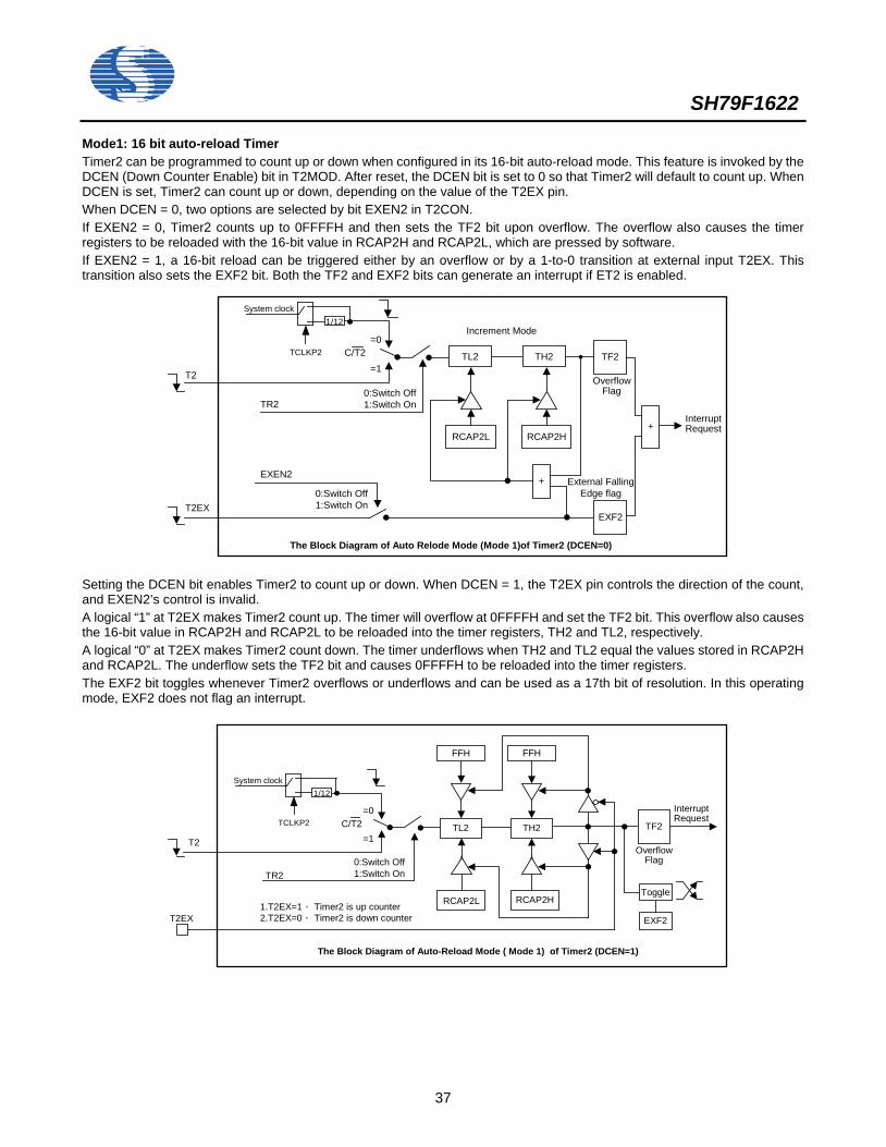
Mode1: 16 bit auto-reload Timer Timer2 can be programmed to count up or down when configured in its 16-bit auto-reload mode. This feature is invoked by the DCEN (Down Counter Enable) bit in T2MOD. After reset, the DCEN bit is set to 0 so that Timer2 will default to count up. When DCEN is set, Timer2 can count up or down, depending on the value of the T2EX pin. When DCEN = 0, two options are selected by bit EXEN2 in T2CON. If EXEN2 = 0, Timer2 counts up to 0FFFFH and then sets the TF2 bit upon overflow. The overflow also causes the timer registers to be reloaded with the 16-bit value in RCAP2H and RCAP2L, which are pressed by software. If EXEN2 = 1, a 16-bit reload can be triggered either by an overflow or by a 1-to-0 transition at external input T2EX. This transition also sets the EXF2 bit. Both the TF2 and EXF2 bits can generate an interrupt if ET2 is enabled.
TF2C/T2=0
=1
The Block Diagram of Auto Relode Mode (Mode 1)of Timer2 (DCEN=0)
RCAP2L RCAP2H
EXF2
+
0:Switch Off1:Switch On
Increment Mode
0:Switch Off1:Switch On
External FallingEdge flag
TL2 TH2
+
T2EX
T2
InterruptRequest
OverflowFlag
TR2
EXEN2
System clock1/12
TCLKP2
Setting the DCEN bit enables Timer2 to count up or down. When DCEN = 1, the T2EX pin controls the direction of the count, and EXEN2’s control is invalid. A logical “1” at T2EX makes Timer2 count up. The timer will overflow at 0FFFFH and set the TF2 bit. This overflow also causes the 16-bit value in RCAP2H and RCAP2L to be reloaded into the timer registers, TH2 and TL2, respectively. A logical “0” at T2EX makes Timer2 count down. The timer underflows when TH2 and TL2 equal the values stored in RCAP2H and RCAP2L. The underflow sets the TF2 bit and causes 0FFFFH to be reloaded into the timer registers. The EXF2 bit toggles whenever Timer2 overflows or underflows and can be used as a 17th bit of resolution. In this operating mode, EXF2 does not flag an interrupt.
TF2
TR2
C/T2
The Block Diagram of Auto-Reload Mode ( Mode 1) of Timer2 (DCEN=1)
T2EX EXF2
Toggle1.T2EX=1, Timer2 is up counter2.T2EX=0, Timer2 is down counter
T2TL2 TH2
RCAP2L RCAP2H
FFH FFH
=0
=1
0:Switch Off1:Switch On
OverflowFlag
InterruptRequest
System clock1/12
TCLKP2
SH79F1622
38
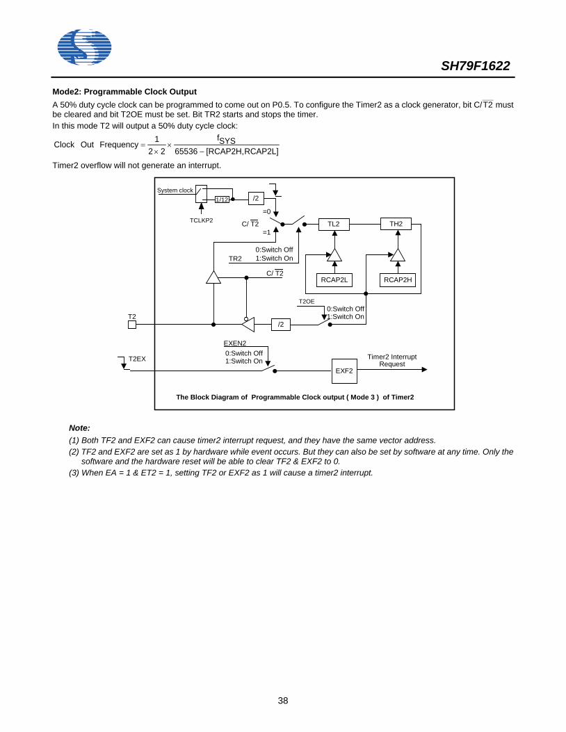
Mode2: Programmable Clock Output A 50% duty cycle clock can be programmed to come out on P0.5. To configure the Timer2 as a clock generator, bit C/T2
———
must be cleared and bit T2OE must be set. Bit TR2 starts and stops the timer. In this mode T2 will output a 50% duty cycle clock:
RCAP2L][RCAP2H,65536SYSf
221FrequencyOutClock
−×
×=
Timer2 overflow will not generate an interrupt.
TR2
=0
=1
The Block Diagram of Programmable Clock output ( Mode 3 ) of Timer2
T2
T2OE
TL2 TH2
RCAP2L RCAP2H
EXEN2
EXF2
0:Switch Off1:Switch OnT2EX
C/ T2
C/ T2
/2
/2
0:Switch Off1:Switch On
Timer2 InterruptRequest
0:Switch Off1:Switch On
System clock1/12
TCLKP2
Note: (1) Both TF2 and EXF2 can cause timer2 interrupt request, and they have the same vector address. (2) TF2 and EXF2 are set as 1 by hardware while event occurs. But they can also be set by software at any time. Only the
software and the hardware reset will be able to clear TF2 & EXF2 to 0. (3) When EA = 1 & ET2 = 1, setting TF2 or EXF2 as 1 will cause a timer2 interrupt.
SH79F1622
39
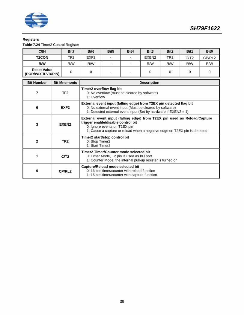
Registers Table 7.24 Timer2 Control Register
C8H Bit7 Bit6 Bit5 Bit4 Bit3 Bit2 Bit1 Bit0 T2CON TF2 EXF2 - - EXEN2 TR2 C/T2
———
CP/RL2————
R/W R/W R/W - - R/W R/W R/W R/W
Reset Value (POR/WDT/LVR/PIN) 0 0 - - 0 0 0 0
Bit Number Bit Mnemonic Description
7 TF2 Timer2 overflow flag bit
0: No overflow (must be cleared by software) 1: Overflow
6 EXF2 External event input (falling edge) from T2EX pin detected flag bit
0: No external event input (Must be cleared by software) 1: Detected external event input (Set by hardware if EXEN2 = 1)
3 EXEN2 External event input (falling edge) from T2EX pin used as Reload/Capture trigger enable/disable control bit
0: Ignore events on T2EX pin 1: Cause a capture or reload when a negative edge on T2EX pin is detected
2 TR2 Timer2 start/stop control bit
0: Stop Timer2 1: Start Timer2
1 C/T2———
Timer2 Timer/Counter mode selected bit
0: Timer Mode, T2 pin is used as I/O port 1: Counter Mode, the internal pull-up resister is turned on
0 CP/RL2————
Capture/Reload mode selected bit
0: 16 bits timer/counter with reload function 1: 16 bits timer/counter with capture function
SH79F1622
40
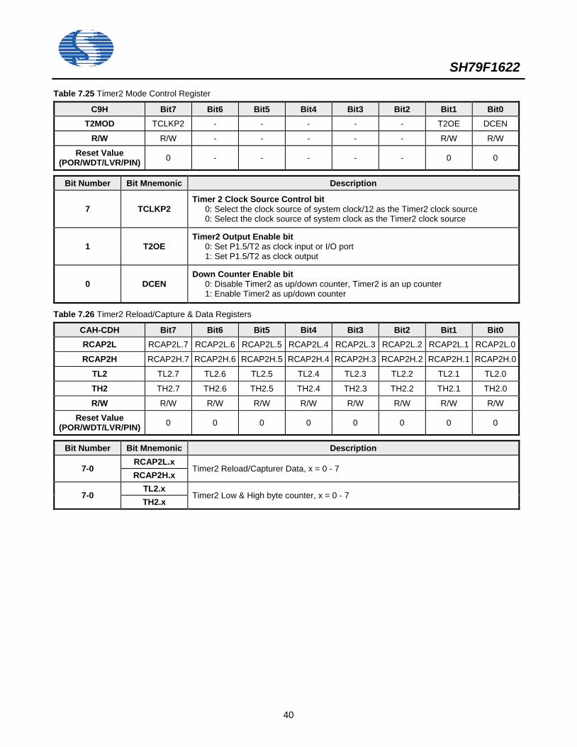
Table 7.25 Timer2 Mode Control Register
C9H Bit7 Bit6 Bit5 Bit4 Bit3 Bit2 Bit1 Bit0 T2MOD TCLKP2 - - - - - T2OE DCEN
R/W R/W - - - - - R/W R/W
Reset Value (POR/WDT/LVR/PIN) 0 - - - - - 0 0
Bit Number Bit Mnemonic Description
7 TCLKP2 Timer 2 Clock Source Control bit
0: Select the clock source of system clock/12 as the Timer2 clock source 0: Select the clock source of system clock as the Timer2 clock source
1 T2OE Timer2 Output Enable bit
0: Set P1.5/T2 as clock input or I/O port 1: Set P1.5/T2 as clock output
0 DCEN Down Counter Enable bit
0: Disable Timer2 as up/down counter, Timer2 is an up counter 1: Enable Timer2 as up/down counter
Table 7.26 Timer2 Reload/Capture & Data Registers
CAH-CDH Bit7 Bit6 Bit5 Bit4 Bit3 Bit2 Bit1 Bit0 RCAP2L RCAP2L.7 RCAP2L.6 RCAP2L.5 RCAP2L.4 RCAP2L.3 RCAP2L.2 RCAP2L.1 RCAP2L.0
RCAP2H RCAP2H.7 RCAP2H.6 RCAP2H.5 RCAP2H.4 RCAP2H.3 RCAP2H.2 RCAP2H.1 RCAP2H.0
TL2 TL2.7 TL2.6 TL2.5 TL2.4 TL2.3 TL2.2 TL2.1 TL2.0
TH2 TH2.7 TH2.6 TH2.5 TH2.4 TH2.3 TH2.2 TH2.1 TH2.0
R/W R/W R/W R/W R/W R/W R/W R/W R/W
Reset Value (POR/WDT/LVR/PIN) 0 0 0 0 0 0 0 0
Bit Number Bit Mnemonic Description
7-0 RCAP2L.x
Timer2 Reload/Capturer Data, x = 0 - 7 RCAP2H.x
7-0 TL2.x
Timer2 Low & High byte counter, x = 0 - 7 TH2.x
SH79F1622
41
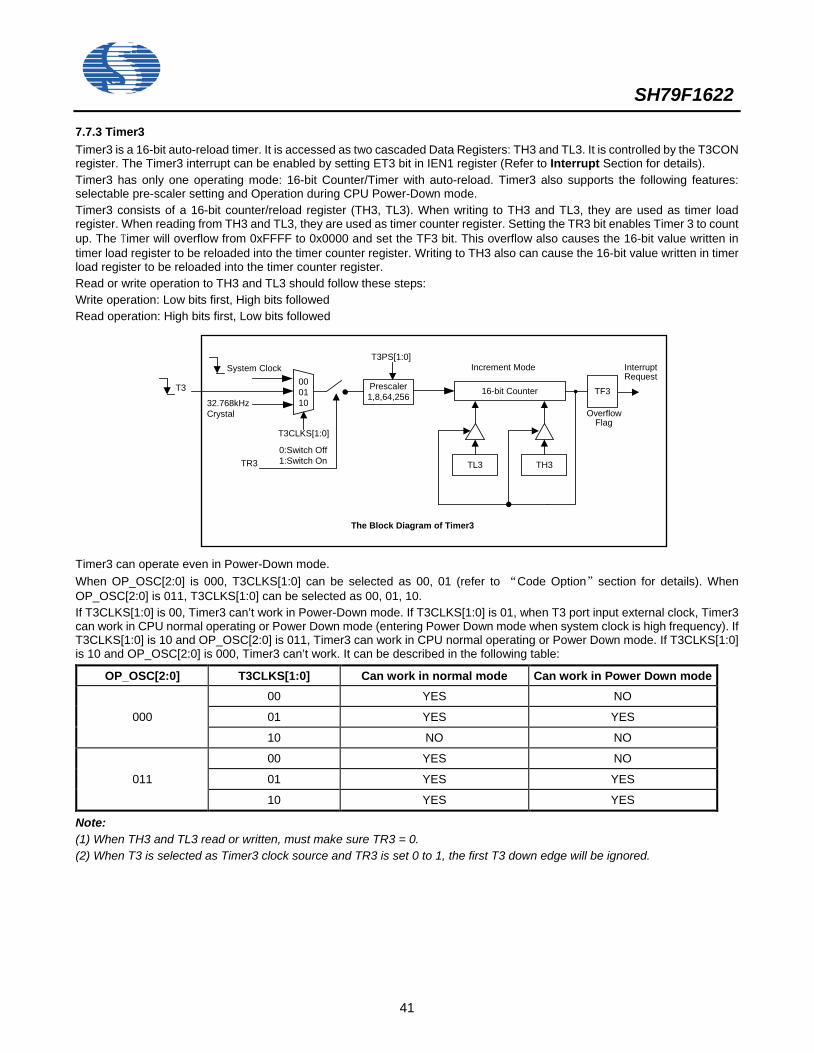
7.7.3 Timer3 Timer3 is a 16-bit auto-reload timer. It is accessed as two cascaded Data Registers: TH3 and TL3. It is controlled by the T3CON register. The Timer3 interrupt can be enabled by setting ET3 bit in IEN1 register (Refer to Interrupt Section for details). Timer3 has only one operating mode: 16-bit Counter/Timer with auto-reload. Timer3 also supports the following features: selectable pre-scaler setting and Operation during CPU Power-Down mode. Timer3 consists of a 16-bit counter/reload register (TH3, TL3). When writing to TH3 and TL3, they are used as timer load register. When reading from TH3 and TL3, they are used as timer counter register. Setting the TR3 bit enables Timer 3 to count up. The Timer will overflow from 0xFFFF to 0x0000 and set the TF3 bit. This overflow also causes the 16-bit value written in timer load register to be reloaded into the timer counter register. Writing to TH3 also can cause the 16-bit value written in timer load register to be reloaded into the timer counter register. Read or write operation to TH3 and TL3 should follow these steps: Write operation: Low bits first, High bits followed Read operation: High bits first, Low bits followed
TF3
The Block Diagram of Timer3
TL3 TH3
Increment Mode
0:Switch Off1:Switch On
16-bit Counter
InterruptRequest
OverflowFlag
TR3
System Clock
Prescaler1,8,64,256
T3PS[1:0]
T3CLKS[1:0]
000110
T3
32.768kHzCrystal
Timer3 can operate even in Power-Down mode. When OP_OSC[2:0] is 000, T3CLKS[1:0] can be selected as 00, 01 (refer to “Code Option”section for details). When OP_OSC[2:0] is 011, T3CLKS[1:0] can be selected as 00, 01, 10. If T3CLKS[1:0] is 00, Timer3 can’t work in Power-Down mode. If T3CLKS[1:0] is 01, when T3 port input external clock, Timer3 can work in CPU normal operating or Power Down mode (entering Power Down mode when system clock is high frequency). If T3CLKS[1:0] is 10 and OP_OSC[2:0] is 011, Timer3 can work in CPU normal operating or Power Down mode. If T3CLKS[1:0] is 10 and OP_OSC[2:0] is 000, Timer3 can’t work. It can be described in the following table:
OP_OSC[2:0] T3CLKS[1:0] Can work in normal mode Can work in Power Down mode
000
00 YES NO
01 YES YES
10 NO NO
011
00 YES NO
01 YES YES
10 YES YES
Note: (1) When TH3 and TL3 read or written, must make sure TR3 = 0. (2) When T3 is selected as Timer3 clock source and TR3 is set 0 to 1, the first T3 down edge will be ignored.
SH79F1622
42
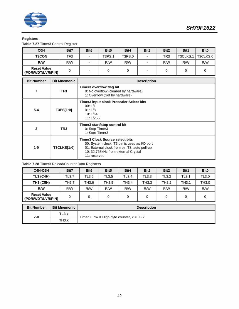
Registers Table 7.27 Timer3 Control Register
C0H Bit7 Bit6 Bit5 Bit4 Bit3 Bit2 Bit1 Bit0 T3CON TF3 - T3PS.1 T3PS.0 - TR3 T3CLKS.1 T3CLKS.0
R/W R/W - R/W R/W - R/W R/W R/W
Reset Value (POR/WDT/LVR/PIN) 0 - 0 0 - 0 0 0
Bit Number Bit Mnemonic Description
7 TF3 Timer3 overflow flag bit
0: No overflow (cleared by hardware) 1: Overflow (Set by hardware)
5-4 T3PS[1:0]
Timer3 input clock Prescaler Select bits 00: 1/1 01: 1/8 10: 1/64 11: 1/256
2 TR3 Timer3 start/stop control bit
0: Stop Timer3 1: Start Timer3
1-0 T3CLKS[1:0]
Timer3 Clock Source select bits 00: System clock, T3 pin is used as I/O port 01: External clock from pin T3, auto pull-up 10: 32.768kHz from external Crystal 11: reserved
Table 7.28 Timer3 Reload/Counter Data Registers
C4H-C5H Bit7 Bit6 Bit5 Bit4 Bit3 Bit2 Bit1 Bit0 TL3 (C4H) TL3.7 TL3.6 TL3.5 TL3.4 TL3.3 TL3.2 TL3.1 TL3.0
TH3 (C5H) TH3.7 TH3.6 TH3.5 TH3.4 TH3.3 TH3.2 TH3.1 TH3.0
R/W R/W R/W R/W R/W R/W R/W R/W R/W
Reset Value (POR/WDT/LVR/PIN) 0 0 0 0 0 0 0 0
Bit Number Bit Mnemonic Description
7-0 TL3.x
Timer3 Low & High byte counter, x = 0 - 7 TH3.x
SH79F1622
43
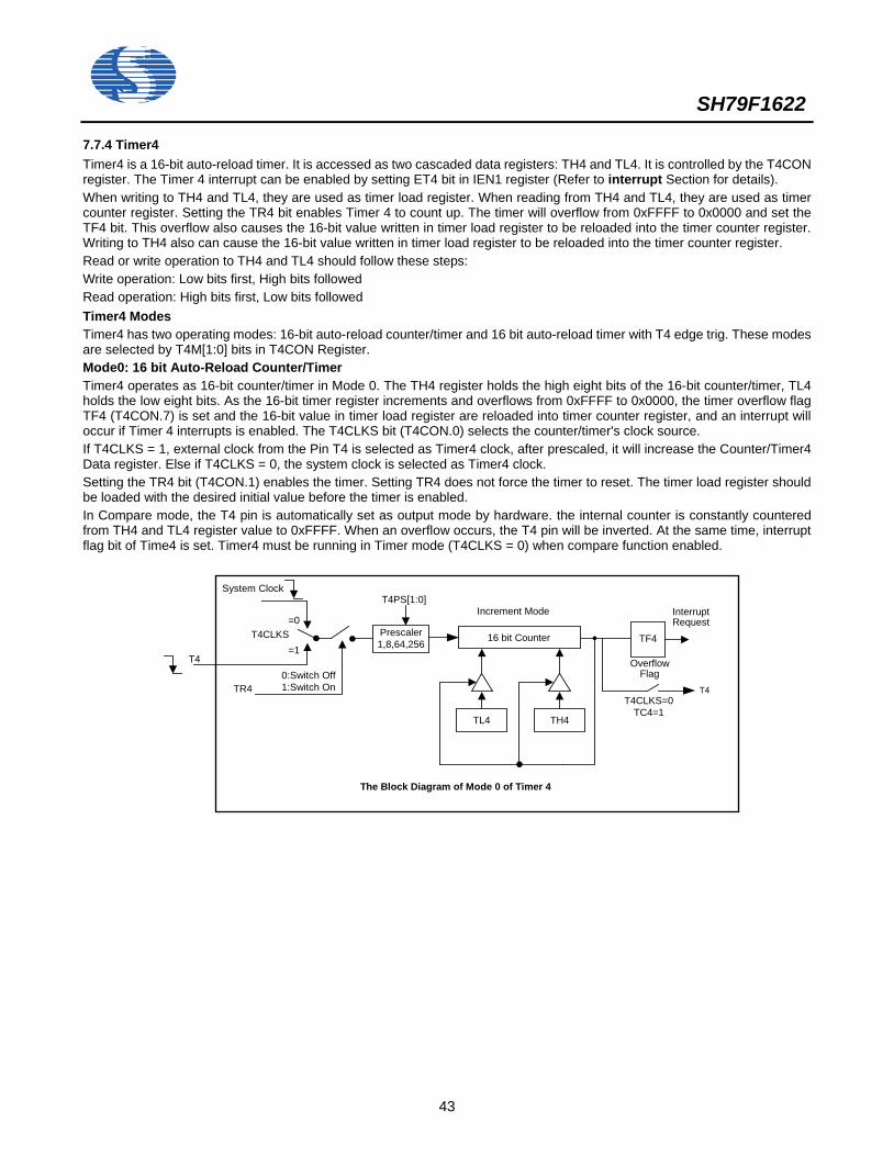
7.7.4 Timer4 Timer4 is a 16-bit auto-reload timer. It is accessed as two cascaded data registers: TH4 and TL4. It is controlled by the T4CON register. The Timer 4 interrupt can be enabled by setting ET4 bit in IEN1 register (Refer to interrupt Section for details). When writing to TH4 and TL4, they are used as timer load register. When reading from TH4 and TL4, they are used as timer counter register. Setting the TR4 bit enables Timer 4 to count up. The timer will overflow from 0xFFFF to 0x0000 and set the TF4 bit. This overflow also causes the 16-bit value written in timer load register to be reloaded into the timer counter register. Writing to TH4 also can cause the 16-bit value written in timer load register to be reloaded into the timer counter register. Read or write operation to TH4 and TL4 should follow these steps: Write operation: Low bits first, High bits followed Read operation: High bits first, Low bits followed Timer4 Modes Timer4 has two operating modes: 16-bit auto-reload counter/timer and 16 bit auto-reload timer with T4 edge trig. These modes are selected by T4M[1:0] bits in T4CON Register. Mode0: 16 bit Auto-Reload Counter/Timer Timer4 operates as 16-bit counter/timer in Mode 0. The TH4 register holds the high eight bits of the 16-bit counter/timer, TL4 holds the low eight bits. As the 16-bit timer register increments and overflows from 0xFFFF to 0x0000, the timer overflow flag TF4 (T4CON.7) is set and the 16-bit value in timer load register are reloaded into timer counter register, and an interrupt will occur if Timer 4 interrupts is enabled. The T4CLKS bit (T4CON.0) selects the counter/timer's clock source. If T4CLKS = 1, external clock from the Pin T4 is selected as Timer4 clock, after prescaled, it will increase the Counter/Timer4 Data register. Else if T4CLKS = 0, the system clock is selected as Timer4 clock. Setting the TR4 bit (T4CON.1) enables the timer. Setting TR4 does not force the timer to reset. The timer load register should be loaded with the desired initial value before the timer is enabled. In Compare mode, the T4 pin is automatically set as output mode by hardware. the internal counter is constantly countered from TH4 and TL4 register value to 0xFFFF. When an overflow occurs, the T4 pin will be inverted. At the same time, interrupt flag bit of Time4 is set. Timer4 must be running in Timer mode (T4CLKS = 0) when compare function enabled.
TF4T4CLKS=0
=1
The Block Diagram of Mode 0 of Timer 4
TL4 TH4
Increment Mode
0:Switch Off1:Switch On
16 bit Counter
T4
InterruptRequest
OverflowFlag
TR4
System Clock
Prescaler1,8,64,256
T4PS[1:0]
T4T4CLKS=0
TC4=1
SH79F1622
44
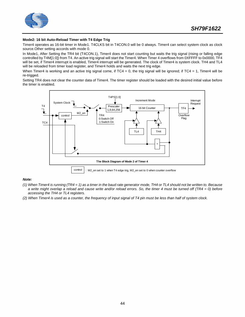
Mode2: 16 bit Auto-Reload Timer with T4 Edge Trig Timer4 operates as 16-bit timer in Mode1. T4CLKS bit in T4CON.0 will be 0 always. Timer4 can select system clock as clock source.Other setting accords with mode 0. In Mode1, After Setting the TR4 bit (T4CON.1), Timer4 does not start counting but waits the trig signal (rising or falling edge controlled by T4M[1:0]) from T4. An active trig signal will start the Timer4. When Timer 4 overflows from 0XFFFF to 0x0000, TF4 will be set, if Timer4 interrupt is enabled, Timer4 interrupt will be generated. The clock of Timer4 is system clock. TH4 and TL4 will be reloaded from timer load register, and Timer4 holds and waits the next trig edge. When Timer4 is working and an active trig signal come, if TC4 = 0, the trig signal will be ignored; if TC4 = 1, Timer4 will be re-trigged. Setting TR4 does not clear the counter data of Timer4. The timer register should be loaded with the desired initial value before the timer is enabled.
TF4
The Block Diagram of Mode 2 of Timer 4
TL4 TH4
Increment Mode
0:Switch Off1:Switch On
16 bit CounterT4
InterruptRequest
OverflowFlag
TR4
System ClockPrescaler1,8,64,256
T4PS[1:0]
+
controlM2_en
TC4
control : M2_en set to 1 when T4 edge trig, M2_en set to 0 when counter overflow
Note:
(1) When Timer4 is running (TR4 = 1) as a timer in the baud rate generator mode, TH4 or TL4 should not be written to. Because a write might overlap a reload and cause write and/or reload errors. So, the timer 4 must be turned off (TR4 = 0) before accessing the TH4 or TL4 registers.
(2) When Timer4 is used as a counter, the frequency of input signal of T4 pin must be less than half of system clock.
SH79F1622
45
Registers Table 7.29 Timer4 Control Register
C2H Bit7 Bit6 Bit5 Bit4 Bit3 Bit2 Bit1 Bit0 T4CON TF4 TC4 T4PS1 T4PS0 T4M1 T4M0 TR4 T4CLKS
R/W R/W R/W R/W R/W R/W R/W R/W R/W
Reset Value (POR/WDT/LVR/PIN) 0 0 0 0 0 0 0 0
Bit Number Bit Mnemonic Description
7 TF4 Timer4 overflow flag bit
0: No overflow (cleared by hardware) 1: Overflow (Set by hardware)
6 TC4
Compare function Enable bit When T4M[1:0] = 00 0: Disable compare function of Timer4 1: Enable compare function of Timer4 When T4M[1:0] = 10 or 11 0: Timer4 can’t be re-trigged 1: Timer4 can be re-trigged
5-4 T4PS[1:0]
Timer4 input clock Prescale Select bits 00: 1/1 01: 1/8 10: 1/64 11: 1/256
3-2 T4M[1:0]
Timer4 Mode Select bit 00: Mode0, 16-bit auto-reload up timer 01: reserved 10: Mode1 with rising edge trig from pin T4 (system clock only, T4CLKS is invalid) 11: Mode1 with falling edge trig from pin T4 (system clock only, T4CLKS is invalid)
1 TR4 Timer4 start/stop control bit
0: Stop Timer4 1: Start Timer4
0 T4CLKS Timer4 Clock Source select bit
0: System clock, T4 pin is used as I/O port 1: External clock from pin T4, the internal pull-up resister is turned on
Table 7.30 Timer4 Reload/Counter Data Registers
D6H-D7H Bit7 Bit6 Bit5 Bit4 Bit3 Bit2 Bit1 Bit0 TL4 TL4.7 TL4.6 TL4.5 TL4.4 TL4.3 TL4.2 TL4.1 TL4.0
TH4 TH4.7 TH4.6 TH4.5 TH4.4 TH4.3 TH4.2 TH4.1 TH4.0
R/W R/W R/W R/W R/W R/W R/W R/W R/W
Reset Value (POR/WDT/LVR/PIN) 0 0 0 0 0 0 0 0
Bit Number Bit Mnemonic Description
7-0 TL4.x
Timer4 Low & High byte counter, x = 0 - 7 TH4.x
SH79F1622
46
7.8 Interrupt 7.8.1 Features
9 interrupt sources 4 interrupt priority levels The SH79F1622 provides total 9 interrupt sources: 4 external interrupts (INT0/1/2/4), 3 timer interrupts (Timer2, 3, 4), one
EUART interrupt, TWI interrupt, TK interrupt. 7.8.2 Interrupt Enable Control Each interrupt source can be individually enabled or disabled by setting or clearing the corresponding bit in the interrupt enable registers IEN0 or IEN1. The IEN0 register also contains global interrupt enable bit, EA, which can enable/disable all the interrupts at once. Generally, after reset, all interrupt enable bits are set to 0, which means that all the interrupts are disabled. 7.8.3 Registers Table 7.31 Primary Interrupt Enable Register
A8H Bit7 Bit6 Bit5 Bit4 Bit3 Bit2 Bit1 Bit0 IEN0 EA - ET2 ES - EX1 TKIE EX0
R/W R/W - R/W R/W - R/W R/W R/W
Reset Value (POR/WDT/LVR/PIN) 0 - 0 0 - 0 0 0
Bit Number Bit Mnemonic Description
7 EA All interrupt enable bit
0: Disable all interrupt 1: Enable all interrupt
5 ET2 Timer2 overflow interrupt enable bit
0: Disable Timer2 overflow interrupt 1: Enable Timer2 overflow interrupt
4 ES EUART interrupt enable bit
0: Disable EUART interrupt 1: Enable EUART interrupt
2 EX1 External interrupt1 enable bit
0: Disable external interrupt1 1: Enable external interrupt1
1 TKIE Touch Key interrupt enable bit
0: Disable Touch Key interrupt 1: Enable Touch Key interrupt
0 EX0 External interrupt0 enable bit
0: Disable external interrupt0 1: Enable external interrupt0
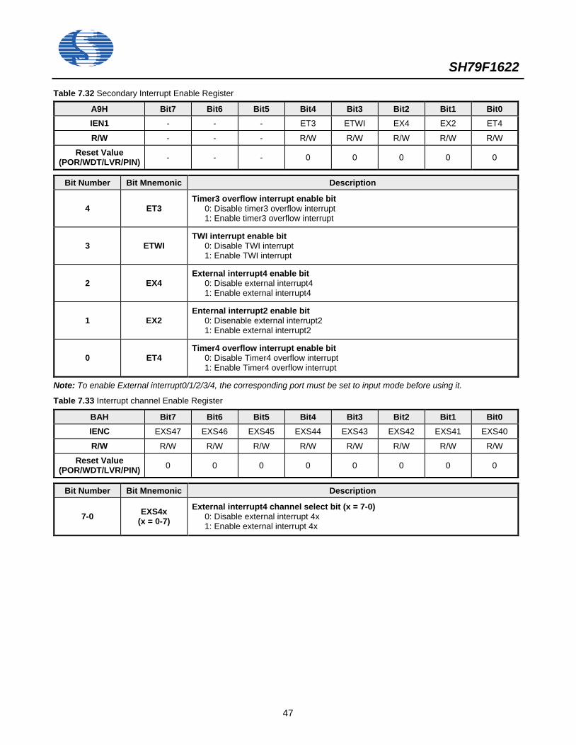
SH79F1622
47
Table 7.32 Secondary Interrupt Enable Register
A9H Bit7 Bit6 Bit5 Bit4 Bit3 Bit2 Bit1 Bit0 IEN1 - - - ET3 ETWI EX4 EX2 ET4
R/W - - - R/W R/W R/W R/W R/W
Reset Value (POR/WDT/LVR/PIN) - - - 0 0 0 0 0
Bit Number Bit Mnemonic Description
4 ET3 Timer3 overflow interrupt enable bit
0: Disable timer3 overflow interrupt 1: Enable timer3 overflow interrupt
3 ETWI TWI interrupt enable bit
0: Disable TWI interrupt 1: Enable TWI interrupt
2 EX4 External interrupt4 enable bit
0: Disable external interrupt4 1: Enable external interrupt4
1 EX2 Enternal interrupt2 enable bit
0: Disenable external interrupt2 1: Enable external interrupt2
0 ET4 Timer4 overflow interrupt enable bit
0: Disable Timer4 overflow interrupt 1: Enable Timer4 overflow interrupt
Note: To enable External interrupt0/1/2/3/4, the corresponding port must be set to input mode before using it.
Table 7.33 Interrupt channel Enable Register
BAH Bit7 Bit6 Bit5 Bit4 Bit3 Bit2 Bit1 Bit0 IENC EXS47 EXS46 EXS45 EXS44 EXS43 EXS42 EXS41 EXS40
R/W R/W R/W R/W R/W R/W R/W R/W R/W
Reset Value (POR/WDT/LVR/PIN) 0 0 0 0 0 0 0 0
Bit Number Bit Mnemonic Description
7-0 EXS4x (x = 0-7)
External interrupt4 channel select bit (x = 7-0) 0: Disable external interrupt 4x 1: Enable external interrupt 4x
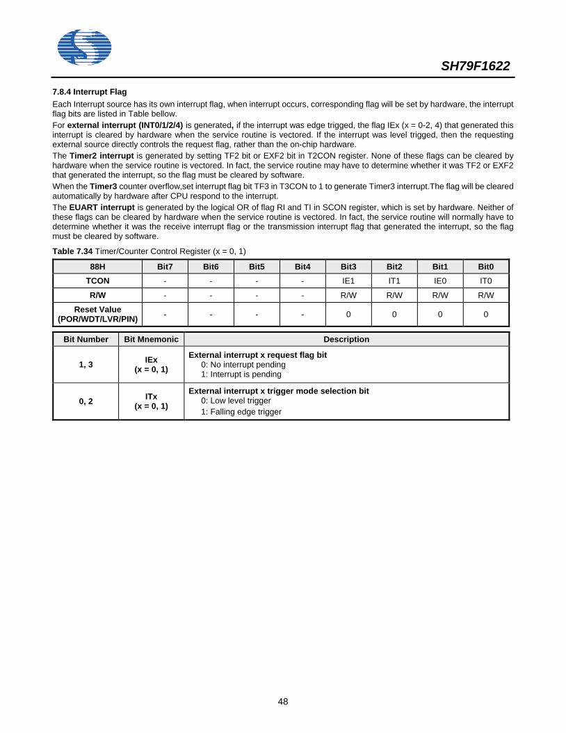
SH79F1622
48
7.8.4 Interrupt Flag Each Interrupt source has its own interrupt flag, when interrupt occurs, corresponding flag will be set by hardware, the interrupt flag bits are listed in Table bellow. For external interrupt (INT0/1/2/4) is generated, if the interrupt was edge trigged, the flag IEx (x = 0-2, 4) that generated this interrupt is cleared by hardware when the service routine is vectored. If the interrupt was level trigged, then the requesting external source directly controls the request flag, rather than the on-chip hardware. The Timer2 interrupt is generated by setting TF2 bit or EXF2 bit in T2CON register. None of these flags can be cleared by hardware when the service routine is vectored. In fact, the service routine may have to determine whether it was TF2 or EXF2 that generated the interrupt, so the flag must be cleared by software. When the Timer3 counter overflow,set interrupt flag bit TF3 in T3CON to 1 to generate Timer3 interrupt.The flag will be cleared automatically by hardware after CPU respond to the interrupt. The EUART interrupt is generated by the logical OR of flag RI and TI in SCON register, which is set by hardware. Neither of these flags can be cleared by hardware when the service routine is vectored. In fact, the service routine will normally have to determine whether it was the receive interrupt flag or the transmission interrupt flag that generated the interrupt, so the flag must be cleared by software.
Table 7.34 Timer/Counter Control Register (x = 0, 1)
88H Bit7 Bit6 Bit5 Bit4 Bit3 Bit2 Bit1 Bit0 TCON - - - - IE1 IT1 IE0 IT0
R/W - - - - R/W R/W R/W R/W
Reset Value (POR/WDT/LVR/PIN) - - - - 0 0 0 0
Bit Number Bit Mnemonic Description
1, 3 IEx (x = 0, 1)
External interrupt x request flag bit 0: No interrupt pending 1: Interrupt is pending
0, 2 ITx (x = 0, 1)
External interrupt x trigger mode selection bit 0: Low level trigger 1: Falling edge trigger
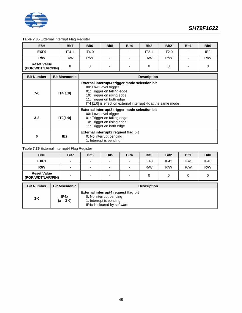
SH79F1622
49
Table 7.35 External Interrupt Flag Register
E8H Bit7 Bit6 Bit5 Bit4 Bit3 Bit2 Bit1 Bit0 EXF0 IT4.1 IT4.0 - - IT2.1 IT2.0 - IE2
R/W R/W R/W - - R/W R/W - R/W
Reset Value (POR/WDT/LVR/PIN) 0 0 - - 0 0 - 0
Bit Number Bit Mnemonic Description
7-6 IT4[1:0]
External interrupt4 trigger mode selection bit 00: Low Level trigger 01: Trigger on falling edge 10: Trigger on rising edge 11: Trigger on both edge IT4 [1:0] is effect on external interrupt 4x at the same mode
3-2 IT2[1:0]
External interrupt2 trigger mode selection bit 00: Low Level trigger 01: Trigger on falling edge 10: Trigger on rising edge 11: Trigger on both edge
0 IE2 External interrupt2 request flag bit
0: No interrupt pending 1: Interrupt is pending
Table 7.36 External Interrupt4 Flag Register
D8H Bit7 Bit6 Bit5 Bit4 Bit3 Bit2 Bit1 Bit0 EXF1 - - - - IF43 IF42 IF41 IF40
R/W - - - - R/W R/W R/W R/W
Reset Value (POR/WDT/LVR/PIN) - - - - 0 0 0 0
Bit Number Bit Mnemonic Description
3-0 IF4x (x = 3-0)
External interrupt4 request flag bit 0: No interrupt pending 1: Interrupt is pending IF4x is cleared by software
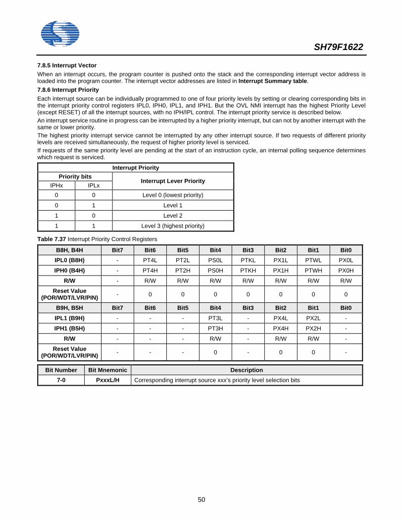
SH79F1622
50
7.8.5 Interrupt Vector When an interrupt occurs, the program counter is pushed onto the stack and the corresponding interrupt vector address is loaded into the program counter. The interrupt vector addresses are listed in Interrupt Summary table. 7.8.6 Interrupt Priority Each interrupt source can be individually programmed to one of four priority levels by setting or clearing corresponding bits in the interrupt priority control registers IPL0, IPH0, IPL1, and IPH1. But the OVL NMI interrupt has the highest Priority Level (except RESET) of all the interrupt sources, with no IPH/IPL control. The interrupt priority service is described below. An interrupt service routine in progress can be interrupted by a higher priority interrupt, but can not by another interrupt with the same or lower priority. The highest priority interrupt service cannot be interrupted by any other interrupt source. If two requests of different priority levels are received simultaneously, the request of higher priority level is serviced. If requests of the same priority level are pending at the start of an instruction cycle, an internal polling sequence determines which request is serviced.
Interrupt Priority Priority bits
Interrupt Lever Priority IPHx IPLx
0 0 Level 0 (lowest priority)
0 1 Level 1
1 0 Level 2
1 1 Level 3 (highest priority)
Table 7.37 Interrupt Priority Control Registers
B8H, B4H Bit7 Bit6 Bit5 Bit4 Bit3 Bit2 Bit1 Bit0 IPL0 (B8H) - PT4L PT2L PS0L PTKL PX1L PTWL PX0L
IPH0 (B4H) - PT4H PT2H PS0H PTKH PX1H PTWH PX0H
R/W - R/W R/W R/W R/W R/W R/W R/W
Reset Value (POR/WDT/LVR/PIN) - 0 0 0 0 0 0 0
B9H, B5H Bit7 Bit6 Bit5 Bit4 Bit3 Bit2 Bit1 Bit0
IPL1 (B9H) - - - PT3L - PX4L PX2L -
IPH1 (B5H) - - - PT3H - PX4H PX2H -
R/W - - - R/W - R/W R/W -
Reset Value (POR/WDT/LVR/PIN) - - - 0 - 0 0 -
Bit Number Bit Mnemonic Description 7-0 PxxxL/H Corresponding interrupt source xxx’s priority level selection bits
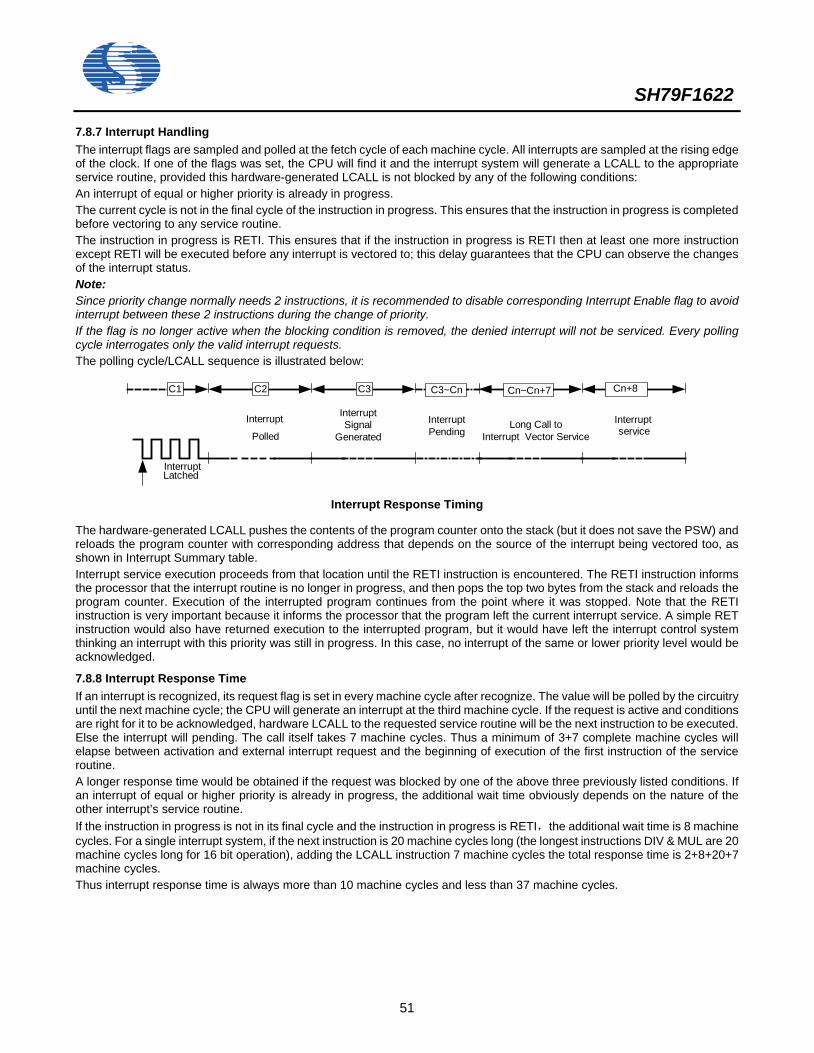
SH79F1622
51
7.8.7 Interrupt Handling The interrupt flags are sampled and polled at the fetch cycle of each machine cycle. All interrupts are sampled at the rising edge of the clock. If one of the flags was set, the CPU will find it and the interrupt system will generate a LCALL to the appropriate service routine, provided this hardware-generated LCALL is not blocked by any of the following conditions: An interrupt of equal or higher priority is already in progress. The current cycle is not in the final cycle of the instruction in progress. This ensures that the instruction in progress is completed before vectoring to any service routine. The instruction in progress is RETI. This ensures that if the instruction in progress is RETI then at least one more instruction except RETI will be executed before any interrupt is vectored to; this delay guarantees that the CPU can observe the changes of the interrupt status. Note: Since priority change normally needs 2 instructions, it is recommended to disable corresponding Interrupt Enable flag to avoid interrupt between these 2 instructions during the change of priority. If the flag is no longer active when the blocking condition is removed, the denied interrupt will not be serviced. Every polling cycle interrogates only the valid interrupt requests. The polling cycle/LCALL sequence is illustrated below:
InterruptLatched
Interrupt
PolledLong Call to
Interrupt Vector Service
Interruptservice
Cn+8C2C1
InterruptPending
C3
InterruptSignal
Generated
C3~Cn Cn~Cn+7
Interrupt Response Timing
The hardware-generated LCALL pushes the contents of the program counter onto the stack (but it does not save the PSW) and reloads the program counter with corresponding address that depends on the source of the interrupt being vectored too, as shown in Interrupt Summary table. Interrupt service execution proceeds from that location until the RETI instruction is encountered. The RETI instruction informs the processor that the interrupt routine is no longer in progress, and then pops the top two bytes from the stack and reloads the program counter. Execution of the interrupted program continues from the point where it was stopped. Note that the RETI instruction is very important because it informs the processor that the program left the current interrupt service. A simple RET instruction would also have returned execution to the interrupted program, but it would have left the interrupt control system thinking an interrupt with this priority was still in progress. In this case, no interrupt of the same or lower priority level would be acknowledged.
7.8.8 Interrupt Response Time If an interrupt is recognized, its request flag is set in every machine cycle after recognize. The value will be polled by the circuitry until the next machine cycle; the CPU will generate an interrupt at the third machine cycle. If the request is active and conditions are right for it to be acknowledged, hardware LCALL to the requested service routine will be the next instruction to be executed. Else the interrupt will pending. The call itself takes 7 machine cycles. Thus a minimum of 3+7 complete machine cycles will elapse between activation and external interrupt request and the beginning of execution of the first instruction of the service routine. A longer response time would be obtained if the request was blocked by one of the above three previously listed conditions. If an interrupt of equal or higher priority is already in progress, the additional wait time obviously depends on the nature of the other interrupt’s service routine. If the instruction in progress is not in its final cycle and the instruction in progress is RETI,the additional wait time is 8 machine cycles. For a single interrupt system, if the next instruction is 20 machine cycles long (the longest instructions DIV & MUL are 20 machine cycles long for 16 bit operation), adding the LCALL instruction 7 machine cycles the total response time is 2+8+20+7 machine cycles. Thus interrupt response time is always more than 10 machine cycles and less than 37 machine cycles.
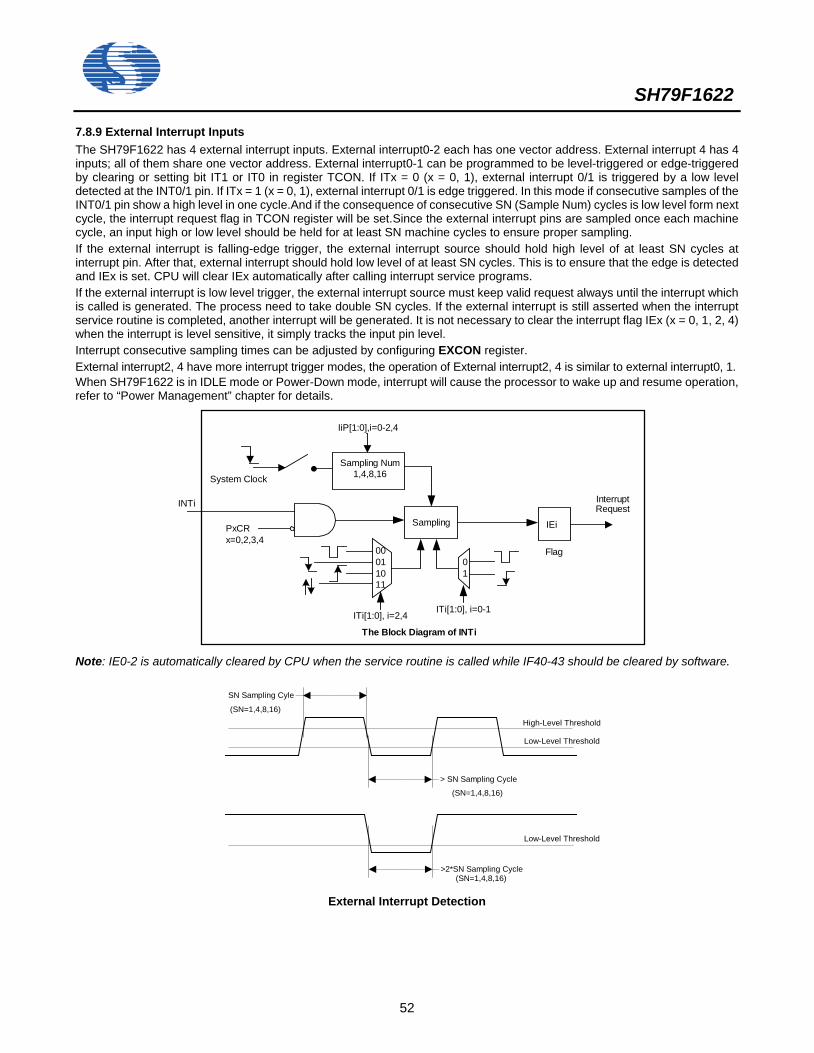
SH79F1622
52
7.8.9 External Interrupt Inputs The SH79F1622 has 4 external interrupt inputs. External interrupt0-2 each has one vector address. External interrupt 4 has 4 inputs; all of them share one vector address. External interrupt0-1 can be programmed to be level-triggered or edge-triggered by clearing or setting bit IT1 or IT0 in register TCON. If ITx = 0 (x = 0, 1), external interrupt 0/1 is triggered by a low level detected at the INT0/1 pin. If ITx = 1 (x = 0, 1), external interrupt 0/1 is edge triggered. In this mode if consecutive samples of the INT0/1 pin show a high level in one cycle.And if the consequence of consecutive SN (Sample Num) cycles is low level form next cycle, the interrupt request flag in TCON register will be set.Since the external interrupt pins are sampled once each machine cycle, an input high or low level should be held for at least SN machine cycles to ensure proper sampling. If the external interrupt is falling-edge trigger, the external interrupt source should hold high level of at least SN cycles at interrupt pin. After that, external interrupt should hold low level of at least SN cycles. This is to ensure that the edge is detected and IEx is set. CPU will clear IEx automatically after calling interrupt service programs. If the external interrupt is low level trigger, the external interrupt source must keep valid request always until the interrupt which is called is generated. The process need to take double SN cycles. If the external interrupt is still asserted when the interrupt service routine is completed, another interrupt will be generated. It is not necessary to clear the interrupt flag IEx (x = 0, 1, 2, 4) when the interrupt is level sensitive, it simply tracks the input pin level. Interrupt consecutive sampling times can be adjusted by configuring EXCON register. External interrupt2, 4 have more interrupt trigger modes, the operation of External interrupt2, 4 is similar to external interrupt0, 1. When SH79F1622 is in IDLE mode or Power-Down mode, interrupt will cause the processor to wake up and resume operation, refer to “Power Management” chapter for details.
IEi
The Block Diagram of INTi
InterruptRequest
Flag
System Clock
IiP[1:0],i=0-2,4
INTi
PxCRx=0,2,3,4
Sampling
00011011
ITi[1:0], i=2,4
01
ITi[1:0], i=0-1
Sampling Num1,4,8,16
Note: IE0-2 is automatically cleared by CPU when the service routine is called while IF40-43 should be cleared by software.
SN Sampling Cyle
> SN Sampling Cycle
High-Level Threshold
Low-Level Threshold
Low-Level Threshold
>2*SN Sampling Cycle
(SN=1,4,8,16)
(SN=1,4,8,16)
(SN=1,4,8,16) External Interrupt Detection
SH79F1622
53
Table 7.38 External interrupt Sampling time Control Register
ADH-AEH Bit7 Bit6 Bit5 Bit4 Bit3 Bit2 Bit1 Bit0 EXCON0 (ADH) - - I2P1 I2P0 I1P1 I1P0 I0P1 I0P0
EXCON1 (AEH) I43P1 I43P0 I42P1 I42P0 I41P1 I41P0 I40P1 I40P0
R/W R/W R/W R/W R/W R/W R/W R/W R/W
Reset Value (POR/WDT/LVR/PIN) 0 0 0 0 0 0 0 0
Bit Number Bit Mnemonic Description
7-0 IxP[1:0] x = 0-3, 41-47
INTx Continuous Sampling time Select bit 00: 1 01: 4 10: 8 11: 16
Note: If IxP[1:0]=01, INTx is falling-edge trigger, interrupt flag will be generated on the condition of continuous sampling 4 times.
7.8.10 Interrupt Summary
Source Vector Address Enable bits Flag bits Polling Priority Interrupt number (c language)
Reset 0000H - - 0 (higest) -
INT0 0003H EX0 IE0 1 0
TK 000BH TKIE IFERR+IFGO+IFAVE +IFCOUNT+IFTKOV 2 1
INT1 0013H EX1 IE1 3 2
EUART 0023H ES RI+TI 4 4
Timer2 002BH ET2 TF2+EXF2 5 5
Timer4 003BH ET4 TF4 6 7
INT2 0043H EX2 IE2 7 8
INT4 004BH EX4+IENC IF43-40 8 9
TWI 0053H ETWI TWINT 9 10
Timer3 005BH ET3 TF3 10 11
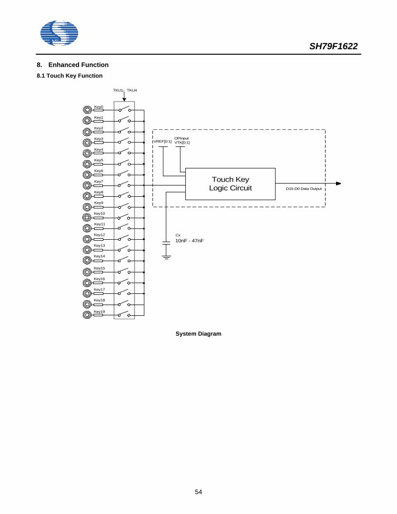
SH79F1622
54
8. Enhanced Function 8.1 Touch Key Function
Key3
Key1
Key0
Key2
Key6
Key5
Key4
Key10
Key8
Key7
Key9
Key12
Key11
Key13
TKU1:TKU4
Key14
Key15
Key16
Key17
Key18
Key19
Cx
10nF - 47nF
D15-D0 Data Output
Touch Key Logic Circuit
VREF[0:1]OPInput VTK[0:1]
System Diagram
SH79F1622
55
Functional Description SH79F1622 built-in Touch Key function module, which can connect at most 20 keys . SH79F1622 built-in simplified operating circuit in Touch Key function module, the application of it only need to use a external connected CX capacitor. The value of CX capacitor choose 22 nF - 44nF, must use polyester capacitor of 10% or more accuracy, X7R capacitor or NPO capacitor. CX capacitor can adjust suitable sensitivity according to the material of actual circuit or medium of Touch Key, the value of capacitor is smaller, the sensitivity is higher, the value of capacitor is higher, the sensitivity is smaller, Touch Key module can select a scan button channel number by TKU1-TKU3 registers, which can connect at most 20 keys. If Touch Key function is not used, it can be set as I/O ports, SEG output or COM output through register.Refer to “I/O Port” chapter for details. On-off circuit can be selected by FSW1 bit and FSW0 bit in register. Working frequency recommend select 4M or below 4M. Touch Key built-in reference voltage, can be selected by VREF1 bit and VREF0 bit in register. Touch Key make sure the stability of data register in dirrerent CX and working frequency by adjusting TUNE1 bit and TUNE0 bit. According to the actual application, Touch Key sampling times can select multi-sampling. Program only need to start one time sampling scan, hardware will perform multi-sampling, count the average value and output result automatically. For example, selecting 6 times sampling output, set TKGO/D
----
O----
N----
E----
bit and start to scan key, hardware will sample 6 times value and campare the six samplied value.Removing maximum and minimum, the rest of them will be averaged to output to16-bit data register. 28-bit amplification coefficient register is used to amplify the calculated result of key controller. If calculated result is larger than 16-bit data, that is to say calculated result is high-bit overflow.The flag bit IFERR will be set. If interrup enables, interrupt program will be called. At the time, user need to reduce data value of amplification coefficient register and restart next scan. Usually during normal operation, the value of 16-bit data register will not be larger than FFFFH. When the value is larger than FFFFH, data value of dividend register will be reduced. Touch Key has 5 kinds of situation to produce interrupt flag bit, any interrupt could be generated, system responds interrupt and perform interrupt subprogram after judging interrupt flag bit: (1) After finishing the key scan, if any abnormal situation does’t happen, IFAVE bit will be set. (2) After finishing the key scan, if calculated result is high-bit overflow, IFERR bit will be set. If multi-sampling, system will stop
current sampling state to wait for next time to restart the scan instead of performing the unfinished sampling continuously.If calculated result high-bit overflow interrupt happens, user should reduce the value of 28-bit amplification coefficient register
(3) Set TKGO/D----
O----
N----
E----
1, system will detect whether comparison output state is normal, if abnormal situation happens, the flag bit IFGO bit will be set. At the same time, key controller startup errors (channel flag register is invalid). User should delay 10uS to restart next scan.
(4) During counting key scan, when counter overflow, interrupt flag bit IFCOUNT will be set, user need to reduce capacitor or slow down switch frequency.
When used as Touch Key, the step of startup as follows: (1) Select key channel which is needed to scan; (2) Set TKCON bit, enable Touch Key module works; (3) Set switch frequency, reference voltage(Vref), key sampling times and the sequence of scan; (4) Set 28-bit amplification coefficient register; (5) Software delay 10uS;
(6) Set TKGO/D----
O----
N----
E----
bit, start key scan; (7) Interrupt generates, TKGO will be cleared by hardware automatically; (8) Judging interrupt flag bit: IFERR, IFGO, IFAVE, IFCOUNT; (9) If IFAVE = 1, reading data register 500H - 527H, program save data result, goto step12;
If IFERR = 1, data register arithmetic overflow error, clear IFERR flag bit, reset amplification coefficient register, reduce the value of amplification coefficient, goto step5 to restart scan; If IFGO = 1, key controller startup errors, clear IFGO flag bit, goto step5 to restart scan (channel flag register is invalid); If IFCOUNT = 1, key scan count overflow error, clear IFCOUNT flag bit, reduce CX capacitor or slow down switch frequency. Goto step5 to restart scan.
(10) Completing A group key scan.
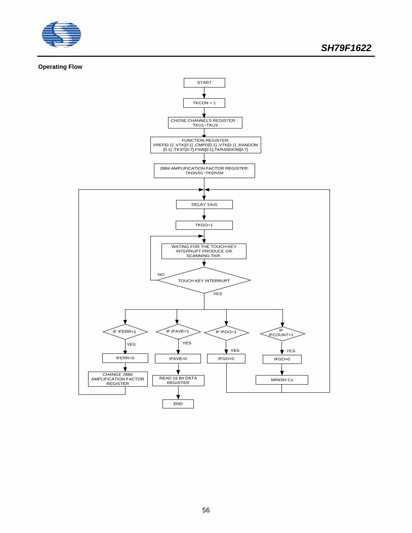
SH79F1622
56
Operating Flow
IF IFAVE=1
CHOSE CHANNELS REGISTER:TKU1~TKU3
FUNCTION REGISTER:VREF[0:1] ,VTK[0:1] ,CMPD[0:1] ,VTK[0:1] ,RANDOM
[0:1] ,TKST[0:7],FSW[0:1],TKRANDOM[0:7]
28Bit AMPLIFICATION FACTOR REGISTER:TKDIV01~TKDIV04
TKGO=1
START
DELAY 10uS
TKCON = 1
READ 16 Bit DATA REGISTER
IF IFGO=1IF IFERR=1
YES
TOUCH KEY INTERRUPT
IFAVE=0
END
WATING FOR THE TOUCH-KEY INTERRUPT PRODUCE OR
SCANNING TKIF.
IFGO=0IFERR=0
CHANGE 28Bit AMPLIFICATION FACTOR
REGISTER
YES
YES
YES
NO
IF IFCOUNT=1
IFGO=0
YES
MINISH Cx
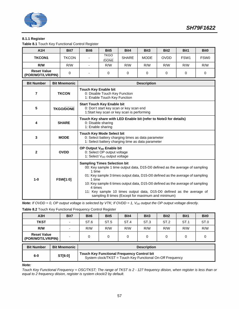
SH79F1622
57
8.1.1 Register Table 8.1 Touch Key Functional Control Register
A1H Bit7 Bit6 Bit5 Bit4 Bit3 Bit2 Bit1 Bit0
TKCON1 TKCON - TKGO /D----
O----
N----
E----
SHARE MODE OVDD FSW1 FSW0
R/W R/W - R/W R/W R/W R/W R/W R/W Reset Value
(POR/WDT/LVR/PIN) 0 - 0 0 0 0 0 0
Bit Number Bit Mnemonic Description
7 TKCON Touch Key Enable bit
0: Disable Touch Key Function 1: Enable Touch Key Function
5 TKGO/D----
O----
N----
E----
Start Touch Key Enable bit
0: Don’t start key scan or key scan end 1:Start key scan or key scan is performing
4 SHARE Touch Key share with LED Enable bit (refer to Note3 for details)
0: Disable sharing 1: Enable sharing
3 MODE Touch Key Mode Select bit
0: Select battery charging times as data parameter 1: Select battery charging time as data parameter
2 OVDD OP Output VDD Enable bit
0: Select OP output voltage 1: Select VDD output voltage
1-0 FSW[1:0]
Sampling Times Selection bit 00: Key sample 1 time output data, D15-D0 defined as the average of sampling
1 time 01: Key sample 3 times output data, D15-D0 defined as the average of sampling
1 time 10: Key sample 6 times output data, D15-D0 defined as the average of sampling
4 times 11: Key sample 10 times output data, D15-D0 defined as the average of
sampling 8 times (Except for maximum and minimum)
Note: If OVDD = 0, OP output voltage is selected by VTK; If OVDD = 1, VDD output the OP output voltage directly.
Table 8.2 Touch Key Functional Frequency Control Register
A3H Bit7 Bit6 Bit5 Bit4 Bit3 Bit2 Bit1 Bit0
TKST - ST.6 ST.5 ST.4 ST.3 ST.2 ST.1 ST.0
R/W - R/W R/W R/W R/W R/W R/W R/W
Reset Value (POR/WDT/LVR/PIN) - 0 0 0 0 0 0 0
Bit Number Bit Mnemonic Description
6-0 ST[6:0] Touch Key Functional Frequency Control bit System clock/TKST = Touch Key Functional On-Off Frequency
Note: Touch Key Functional Frequency = OSC/TKST; The range of TKST is 2 - 127 frequency diision, when register is less than or equal to 2 frequency diision, register is system ckock/2 by default.
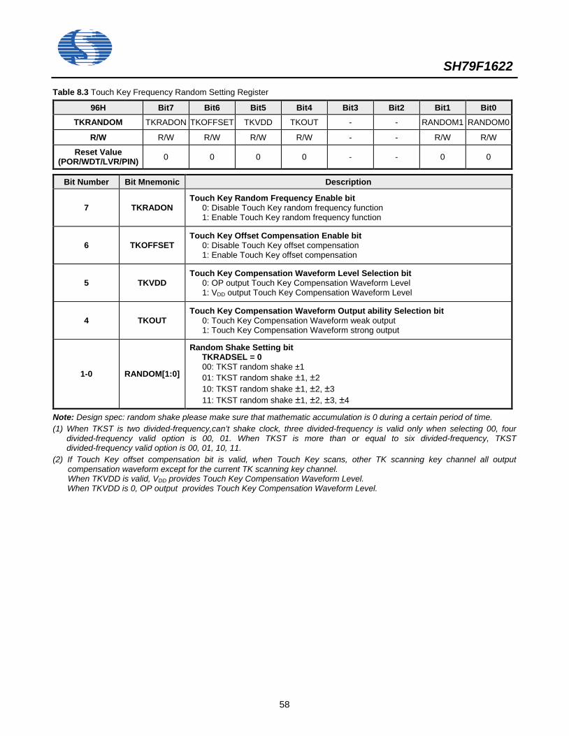
SH79F1622
58
Table 8.3 Touch Key Frequency Random Setting Register
96H Bit7 Bit6 Bit5 Bit4 Bit3 Bit2 Bit1 Bit0
TKRANDOM TKRADON TKOFFSET TKVDD TKOUT - - RANDOM1 RANDOM0
R/W R/W R/W R/W R/W - - R/W R/W
Reset Value (POR/WDT/LVR/PIN) 0 0 0 0 - - 0 0
Bit Number Bit Mnemonic Description
7 TKRADON Touch Key Random Frequency Enable bit
0: Disable Touch Key random frequency function 1: Enable Touch Key random frequency function
6 TKOFFSET Touch Key Offset Compensation Enable bit
0: Disable Touch Key offset compensation 1: Enable Touch Key offset compensation
5 TKVDD Touch Key Compensation Waveform Level Selection bit
0: OP output Touch Key Compensation Waveform Level 1: VDD output Touch Key Compensation Waveform Level
4 TKOUT Touch Key Compensation Waveform Output ability Selection bit
0: Touch Key Compensation Waveform weak output 1: Touch Key Compensation Waveform strong output
1-0 RANDOM[1:0]
Random Shake Setting bit TKRADSEL = 0 00: TKST random shake ±1 01: TKST random shake ±1, ±2 10: TKST random shake ±1, ±2, ±3 11: TKST random shake ±1, ±2, ±3, ±4
Note: Design spec: random shake please make sure that mathematic accumulation is 0 during a certain period of time. (1) When TKST is two divided-frequency,can’t shake clock, three divided-frequency is valid only when selecting 00, four
divided-frequency valid option is 00, 01. When TKST is more than or equal to six divided-frequency, TKST divided-frequency valid option is 00, 01, 10, 11.
(2) If Touch Key offset compensation bit is valid, when Touch Key scans, other TK scanning key channel all output compensation waveform except for the current TK scanning key channel. When TKVDD is valid, VDD provides Touch Key Compensation Waveform Level. When TKVDD is 0, OP output provides Touch Key Compensation Waveform Level.
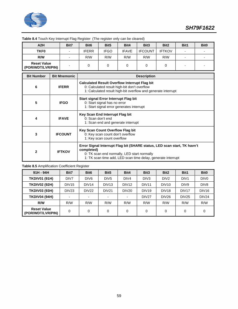
SH79F1622
59
Table 8.4 Touch Key Interrupt Flag Register (The register only can be cleared)
A2H Bit7 Bit6 Bit5 Bit4 Bit3 Bit2 Bit1 Bit0 TKF0 - IFERR IFGO IFAVE IFCOUNT IFTKOV - -
R/W - R/W R/W R/W R/W R/W - -
Reset Value (POR/WDT/LVR/PIN) - 0 0 0 0 0 - -
Bit Number Bit Mnemonic Description
6 IFERR Calculated Result Overflow Interrupt Flag bit
0: Calculated result high-bit don’t overflow 1: Calculated result high-bit overflow and generate interrupt
5 IFGO Start signal Error Interrupt Flag bit
0: Start signal has no error 1: Start signal error generates interrupt
4 IFAVE Key Scan End Interrupt Flag bit
0: Scan don’t end 1: Scan end and generate interrupt
3 IFCOUNT Key Scan Count Overflow Flag bit
0: Key scan count don’t overflow 1: Key scan count overflow
2 IFTKOV Error Signal Interrupt Flag bit (SHARE status, LED scan start, TK havn’t completed)
0: TK scan end normally, LED start normally 1: TK scan time add, LED scan time delay, generate interrupt
Table 8.5 Amplification Coefficient Register
91H - 94H Bit7 Bit6 Bit5 Bit4 Bit3 Bit2 Bit1 Bit0 TKDIV01 (91H) DIV7 DIV6 DIV5 DIV4 DIV3 DIV2 DIV1 DIV0
TKDIV02 (92H) DIV15 DIV14 DIV13 DIV12 DIV11 DIV10 DIV9 DIV8
TKDIV03 (93H) DIV23 DIV22 DIV21 DIV20 DIV19 DIV18 DIV17 DIV16
TKDIV04 (94H) - - - - DIV27 DIV26 DIV25 DIV24
R/W R/W R/W R/W R/W R/W R/W R/W R/W
Reset Value (POR/WDT/LVR/PIN) 0 0 0 0 0 0 0 0
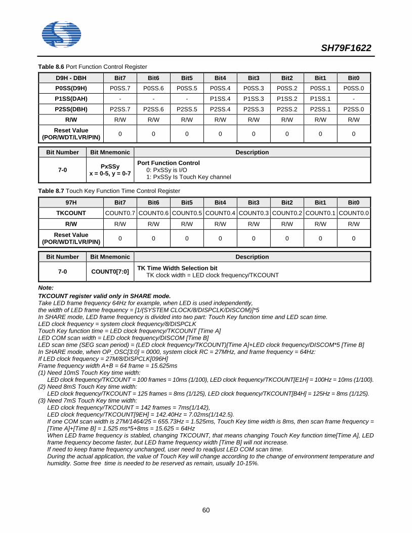
SH79F1622
60
Table 8.6 Port Function Control Register
D9H - DBH Bit7 Bit6 Bit5 Bit4 Bit3 Bit2 Bit1 Bit0 P0SS(D9H) P0SS.7 P0SS.6 P0SS.5 P0SS.4 P0SS.3 P0SS.2 P0SS.1 P0SS.0
P1SS(DAH) - - - P1SS.4 P1SS.3 P1SS.2 P1SS.1 -
P2SS(DBH) P2SS.7 P2SS.6 P2SS.5 P2SS.4 P2SS.3 P2SS.2 P2SS.1 P2SS.0
R/W R/W R/W R/W R/W R/W R/W R/W R/W
Reset Value (POR/WDT/LVR/PIN) 0 0 0 0 0 0 0 0
Bit Number Bit Mnemonic Description
7-0 PxSSy x = 0-5, y = 0-7
Port Function Control 0: PxSSy is I/O 1: PxSSy Is Touch Key channel
Table 8.7 Touch Key Function Time Control Register
97H Bit7 Bit6 Bit5 Bit4 Bit3 Bit2 Bit1 Bit0
TKCOUNT COUNT0.7 COUNT0.6 COUNT0.5 COUNT0.4 COUNT0.3 COUNT0.2 COUNT0.1 COUNT0.0
R/W R/W R/W R/W R/W R/W R/W R/W R/W
Reset Value (POR/WDT/LVR/PIN) 0 0 0 0 0 0 0 0
Bit Number Bit Mnemonic Description
7-0 COUNT0[7:0] TK Time Width Selection bit TK clock width = LED clock frequency/TKCOUNT
Note: TKCOUNT register valid only in SHARE mode. Take LED frame frequency 64Hz for example, when LED is used independently, the width of LED frame frequency = [1/(SYSTEM CLOCK/8/DISPCLK/DISCOM)]*5 In SHARE mode, LED frame frequency is divided into two part: Touch Key function time and LED scan time. LED clock frequency = system clock frequency/8/DISPCLK Touch Key function time = LED clock frequency/TKCOUNT [Time A] LED COM scan width = LED clock frequency/DISCOM [Time B] LED scan time (SEG scan period) = (LED clock frequency/TKCOUNT)[Time A]+LED clock frequency/DISCOM*5 [Time B] In SHARE mode, when OP_OSC[3:0] = 0000, system clock RC = 27MHz, and frame frequency = 64Hz: If LED clock frequency = 27M/8/DISPCLK[096H] Frame frequency width A+B = 64 frame = 15.625ms (1) Need 10mS Touch Key time width:
LED clock frequency/TKCOUNT = 100 frames = 10ms (1/100), LED clock frequency/TKCOUNT[E1H] = 100Hz = 10ms (1/100). (2) Need 8mS Touch Key time width:
LED clock frequency/TKCOUNT = 125 frames = 8ms (1/125), LED clock frequency/TKCOUNT[B4H] = 125Hz = 8ms (1/125). (3) Need 7mS Touch Key time width:
LED clock frequency/TKCOUNT = 142 frames = 7ms(1/142), LED clock frequency/TKCOUNT[9EH] = 142.40Hz = 7.02ms(1/142.5). If one COM scan width is 27M/1464/25 = 655.73Hz = 1.525ms, Touch Key time width is 8ms, then scan frame frequency = [Time A]+[Time B] = 1.525 ms*5+8ms = 15.625 = 64Hz When LED frame frequency is stabled, changing TKCOUNT, that means changing Touch Key function time[Time A], LED frame frequency become faster, but LED frame frequency width [Time B] will not increase. If need to keep frame frequency unchanged, user need to readjust LED COM scan time. During the actual application, the value of Touch Key will change according to the change of environment temperature and humidity. Some free time is needed to be reserved as remain, usually 10-15%.
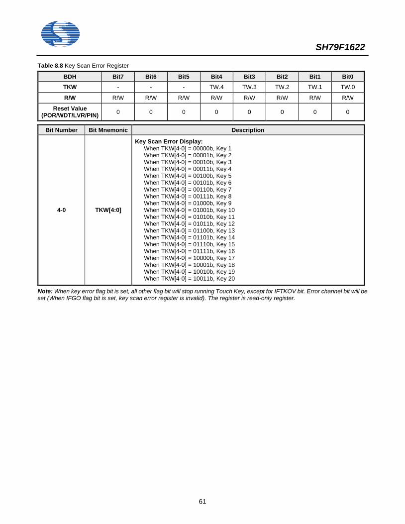
SH79F1622
61
Table 8.8 Key Scan Error Register
BDH Bit7 Bit6 Bit5 Bit4 Bit3 Bit2 Bit1 Bit0
TKW - - - TW.4 TW.3 TW.2 TW.1 TW.0
R/W R/W R/W R/W R/W R/W R/W R/W R/W
Reset Value (POR/WDT/LVR/PIN) 0 0 0 0 0 0 0 0
Bit Number Bit Mnemonic Description
4-0 TKW[4:0]
Key Scan Error Display: When TKW[4-0] = 00000b, Key 1 When TKW[4-0] = 00001b, Key 2 When TKW[4-0] = 00010b, Key 3 When TKW[4-0] = 00011b, Key 4 When TKW[4-0] = 00100b, Key 5 When TKW[4-0] = 00101b, Key 6 When TKW[4-0] = 00110b, Key 7 When TKW[4-0] = 00111b, Key 8 When TKW[4-0] = 01000b, Key 9 When TKW[4-0] = 01001b, Key 10 When TKW[4-0] = 01010b, Key 11 When TKW[4-0] = 01011b, Key 12 When TKW[4-0] = 01100b, Key 13 When TKW[4-0] = 01101b, Key 14 When TKW[4-0] = 01110b, Key 15 When TKW[4-0] = 01111b, Key 16 When TKW[4-0] = 10000b, Key 17 When TKW[4-0] = 10001b, Key 18 When TKW[4-0] = 10010b, Key 19 When TKW[4-0] = 10011b, Key 20
Note: When key error flag bit is set, all other flag bit will stop running Touch Key, except for IFTKOV bit. Error channel bit will be set (When IFGO flag bit is set, key scan error register is invalid). The register is read-only register.
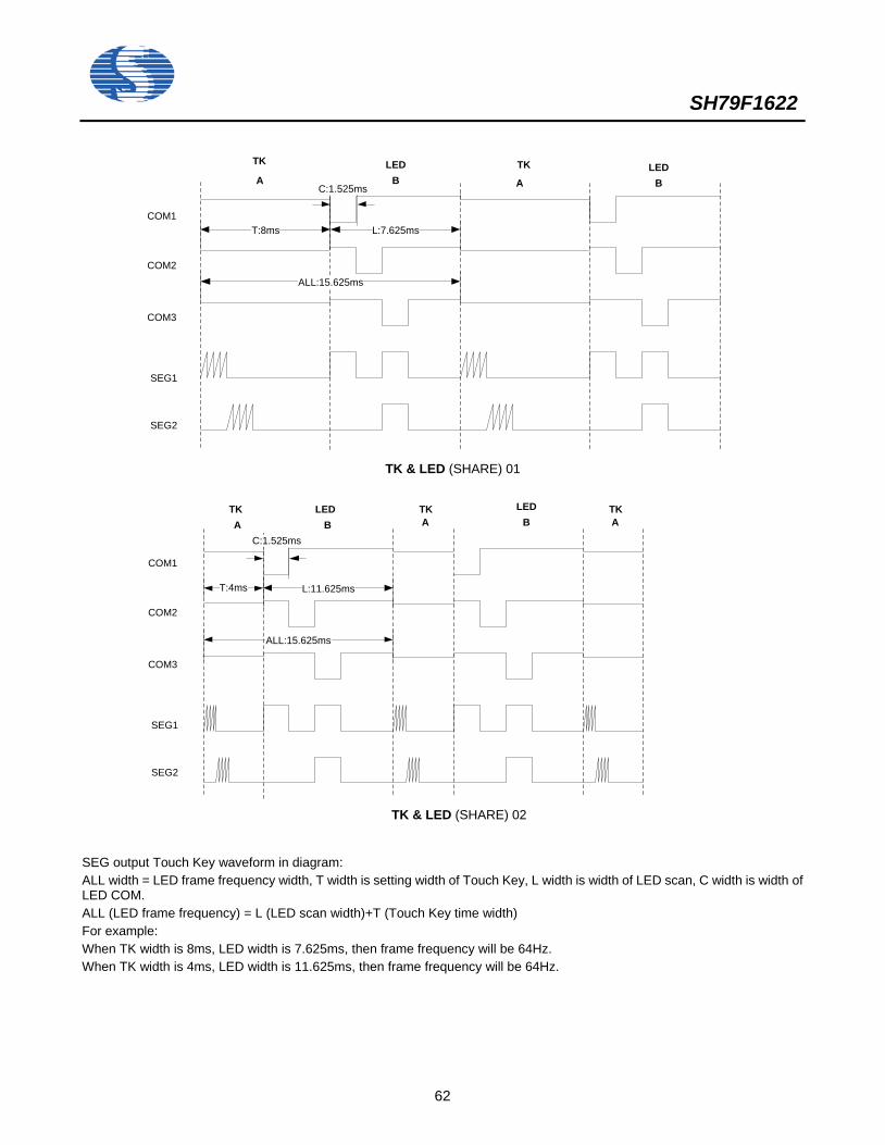
SH79F1622
62
LEDB
TK
ATK
A
COM1
COM2
COM3
SEG1
SEG2
TK & LED (SHARE) 01
LEDB
T:8ms L:7.625ms
ALL:15.625ms
LEDB
TKA
TKA
COM1
COM2
COM3
SEG1
SEG2
TK & LED (SHARE) 02
LEDB
T:4ms L:11.625ms
ALL:15.625ms
TKA
C:1.525ms
C:1.525ms
SEG output Touch Key waveform in diagram: ALL width = LED frame frequency width, T width is setting width of Touch Key, L width is width of LED scan, C width is width of LED COM. ALL (LED frame frequency) = L (LED scan width)+T (Touch Key time width) For example: When TK width is 8ms, LED width is 7.625ms, then frame frequency will be 64Hz. When TK width is 4ms, LED width is 11.625ms, then frame frequency will be 64Hz.
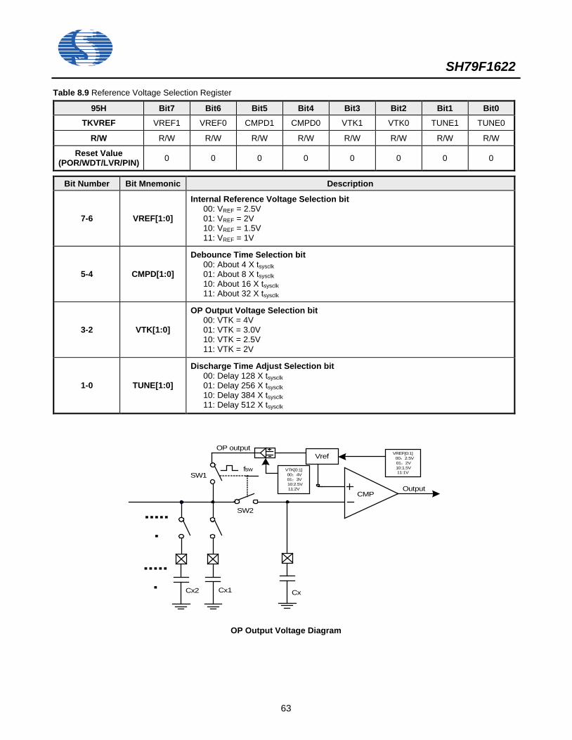
SH79F1622
63
Table 8.9 Reference Voltage Selection Register
95H Bit7 Bit6 Bit5 Bit4 Bit3 Bit2 Bit1 Bit0
TKVREF VREF1 VREF0 CMPD1 CMPD0 VTK1 VTK0 TUNE1 TUNE0
R/W R/W R/W R/W R/W R/W R/W R/W R/W
Reset Value (POR/WDT/LVR/PIN) 0 0 0 0 0 0 0 0
Bit Number Bit Mnemonic Description
7-6 VREF[1:0]
Internal Reference Voltage Selection bit 00: VREF = 2.5V 01: VREF = 2V 10: VREF = 1.5V 11: VREF = 1V
5-4 CMPD[1:0]
Debounce Time Selection bit 00: About 4 X tsysclk 01: About 8 X tsysclk 10: About 16 X tsysclk 11: About 32 X tsysclk
3-2 VTK[1:0]
OP Output Voltage Selection bit 00: VTK = 4V 01: VTK = 3.0V 10: VTK = 2.5V 11: VTK = 2V
1-0 TUNE[1:0]
Discharge Time Adjust Selection bit 00: Delay 128 X tsysclk 01: Delay 256 X tsysclk 10: Delay 384 X tsysclk 11: Delay 512 X tsysclk
OP output
SW1
SW2
CMPOutput
...... Cx1Cx2
......
fsw
Vref
VTK[0:1]00:4V01:3V10:2.5V11:2V
VREF[0:1]00:2.5V01:2V10:1.5V11:1V
Cx
OP Output Voltage Diagram
SH79F1622
64
Table 8.10 Key Scan Sequence Register
A4H - A6H Bit7 Bit6 Bit5 Bit4 Bit3 Bit2 Bit1 Bit0
TKU1 (A4H) TK8 TK7 TK6 TK5 TK4 TK3 TK2 TK1
TKU2 (A5H) TK16 TK15 TK14 TK13 TK12 TK11 TK10 TK9
TKU3 (A6H) - - - - TK20 TK19 TK18 TK17
R/W R/W R/W R/W R/W R/W R/W R/W R/W
Reset Value (POR/WDT/LVR/PIN) 0 0 0 0 0 0 0 0
Note: When share bit is set, TK17 - 20 wil be used as COM output, key scan is invalid. When some bit of TKU1 - TKU3 is cleared, starting key scan will skip the channel of this key. The sequence of key scan is from TK1 in TKU1 to TK20 in TKU3, representing 20 channels of key scan separately.
Table 8.11 16-bit Data Register(Touch Key data RAM is read-only register)
Address Bit7 Bit6 Bit5 Bit4 Bit3 Bit2 Bit1 Bit0 500H TK01L D7 D6 D5 D4 D3 D2 D1 D0
501H TK01H D15 D14 D13 D12 D11 D10 D9 D8
502H TK02L D7 D6 D5 D4 D3 D2 D1 D0
503H TK02H D15 D14 D13 D12 D11 D10 D9 D8
504H TK03L D7 D6 D5 D4 D3 D2 D1 D0
505H TK03H D15 D14 D13 D12 D11 D10 D9 D8
506H TK04L D7 D6 D5 D4 D3 D2 D1 D0
507H TK04H D15 D14 D13 D12 D11 D10 D9 D8
508H TK05L D7 D6 D5 D4 D3 D2 D1 D0
509H TK05H D15 D14 D13 D12 D11 D10 D9 D8
50AH TK06L D7 D6 D5 D4 D3 D2 D1 D0
50BH TK06H D15 D14 D13 D12 D11 D10 D9 D8
50CH TK07L D7 D6 D5 D4 D3 D2 D1 D0
50DH TK07H D15 D14 D13 D12 D11 D10 D9 D8
50EH TK08L D7 D6 D5 D4 D3 D2 D1 D0
50FH TK08H D15 D14 D13 D12 D11 D10 D9 D8
510H TK09L D7 D6 D5 D4 D3 D2 D1 D0
511H TK09H D15 D14 D13 D12 D11 D10 D9 D8
512H TK010L D7 D6 D5 D4 D3 D2 D1 D0
513H TK010H D15 D14 D13 D12 D11 D10 D9 D8
514H TK011L D7 D6 D5 D4 D3 D2 D1 D0
515H TK011H D15 D14 D13 D12 D11 D10 D9 D8
516H TK012L D7 D6 D5 D4 D3 D2 D1 D0
517H TK012H D15 D14 D13 D12 D11 D10 D9 D8
518H TK013L D7 D6 D5 D4 D3 D2 D1 D0
519H TK013H D15 D14 D13 D12 D11 D10 D9 D8
(to be continued)
SH79F1622
65
(continue)
51AH TK014L D7 D6 D5 D4 D3 D2 D1 D0
51BH TK014H D15 D14 D13 D12 D11 D10 D9 D8
51CH TK015L D7 D6 D5 D4 D3 D2 D1 D0
51DH TK015H D15 D14 D13 D12 D11 D10 D9 D8
51EH TK016L D7 D6 D5 D4 D3 D2 D1 D0
51FH TK016H D15 D14 D13 D12 D11 D10 D9 D8
520H TK017L D7 D6 D5 D4 D3 D2 D1 D0
521H TK017H D15 D14 D13 D12 D11 D10 D9 D8
522H TK018L D7 D6 D5 D4 D3 D2 D1 D0
523H TK018H D15 D14 D13 D12 D11 D10 D9 D8
524H TK019L D7 D6 D5 D4 D3 D2 D1 D0
525H TK019H D15 D14 D13 D12 D11 D10 D9 D8
526H TK020L D7 D6 D5 D4 D3 D2 D1 D0
527H TK020H D15 D14 D13 D12 D11 D10 D9 D8
Note: (1) OP output voltage is supply voltage of Touch Key, Vref is reference voltage source of Touch Key. (2) Touch Key can adjust discharge time of capacitor by setting TUNE1 bit and TUNE0 bit to ensure the stability of data register
under the condition of different Cx and working frequency. (3) When enable LED share with Touch Key: TK1 - TK16 will be used as key, P1.1 - P1.6 is used as COM, TK17 - TK20 is
invalid.Completing Touch Key function scan will exit Touch Key module.It is need to set SEG and COM before enabling LED display module. The content of scanning COM1 - COM7, SEG0 - 15 need to be prestored. LED function is finished and restart Touch Key function after a scanning.
SH79F1622
66
8.2 LED Driver LED dirver contains a controller, 7 COM output pins and 16 SEG output pins, supporting 1/4 - 1/7 duty voltage drive mode. When DISPSEL bit is set, LED function is enable. Controller consists of display data RAM storage area and a duty generator. LED SEG1-SEG16 can also be used as I/O port. P0SS register and P2SS register is invalid, SEG01 register and SEG02 register will be used to control the mode selection of LED_SEG1-16, COM1-COM7 and I/O port. LED will be closed during power-on reset, pin reset, LVR reset or WDT reset. 8.2.1 Register Table 8.12 LED Control Register
89H Bit7 Bit6 Bit5 Bit4 Bit3 Bit2 Bit1 Bit0 DISPCON - LEDON - - - - DUTY1 DUTY0
R/W - R/W - - - - R/W R/W
Reset Value (POR/WDT/LVR/PIN) - 0 - - - - 0 0
Bit Number Bit Mnemonic Description
6 LEDON LED Enable Control bit
0: Disable LED Driver 1: Enable LED Drive
1-0 DUTY[1:0]
Duty Selection bit 00: 1/4 duty 01: 1/5 duty 10: 1/6 duty 11: 1/7 duty
Table 8.13 LED Clock Control Register
8CH Bit7 Bit6 Bit5 Bit4 Bit3 Bit2 Bit1 Bit0 DISPCLK DCK0.7 DCK0.6 DCK0.5 DCK0.4 DCK0.3 DCK0.2 DCK0.1 DCK0.0
R/W R/W R/W R/W R/W R/W R/W R/W R/W
Reset Value (POR/WDT/LVR/PIN) 0 0 0 0 0 0 0 0
Bit Number Bit Mnemonic Description
7-0 DCK0[7:0] LED Clock Selection bit LED clock frequency = system clock frequency/8/DISPCLK
Table 8.14 COM Scan Width Control Register
9FH Bit7 Bit6 Bit5 Bit4 Bit3 Bit2 Bit1 Bit0 DISCOM DCOM.7 DCOM.6 DCOM.5 DCOM.4 DCOM.3 DCOM.2 DCOM.1 DCOM.0
R/W R/W R/W R/W R/W R/W R/W R/W R/W
Reset Value (POR/WDT/LVR/PIN) 0 0 0 0 0 0 0 0
Bit Number Bit Mnemonic Description
7-0 DCOM[7:0] LED One COM Scan Width Selection bit One COM Scan Width = LED clock frequency/DISCOM
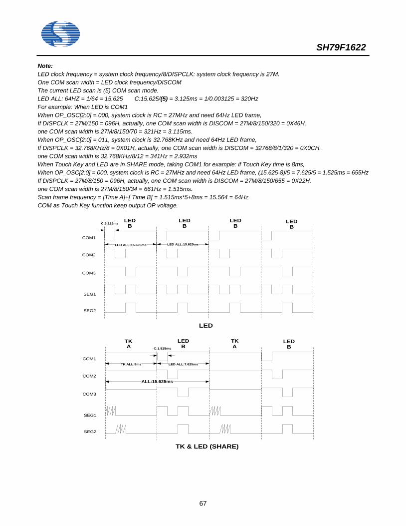
SH79F1622
67
Note: LED clock frequency = system clock frequency/8/DISPCLK: system clock frequency is 27M. One COM scan width = LED clock frequency/DISCOM The current LED scan is (5) COM scan mode. LED ALL: 64HZ = 1/64 = 15.625 C:15.625/(5) = 3.125ms = 1/0.003125 = 320Hz For example: When LED is COM1 When OP_OSC[2:0] = 000, system clock is RC = 27MHz and need 64Hz LED frame, If DISPCLK = 27M/150 = 096H, actually, one COM scan width is DISCOM = 27M/8/150/320 = 0X46H. one COM scan width is 27M/8/150/70 = 321Hz = 3.115ms. When OP_OSC[2:0] = 011, system clock is 32.768KHz and need 64Hz LED frame, If DISPCLK = 32.768KHz/8 = 0X01H, actually, one COM scan width is DISCOM = 32768/8/1/320 = 0X0CH. one COM scan width is 32.768KHz/8/12 = 341Hz = 2.932ms When Touch Key and LED are in SHARE mode, taking COM1 for example: if Touch Key time is 8ms, When OP_OSC[2:0] = 000, system clock is RC = 27MHz and need 64Hz LED frame, (15.625-8)/5 = 7.625/5 = 1.525ms = 655Hz If DISPCLK = 27M/8/150 = 096H, actually, one COM scan width is DISCOM = 27M/8/150/655 = 0X22H. one COM scan width is 27M/8/150/34 = 661Hz = 1.515ms. Scan frame frequency = [Time A]+[ Time B] = 1.515ms*5+8ms = 15.564 = 64Hz COM as Touch Key function keep output OP voltage.
LEDB
TKA
TKA
COM1
COM2
COM3
SEG1
SEG2
COM1
COM2
COM3
SEG1
SEG2
LED
TK & LED (SHARE)
LEDB
LEDB
LEDB
LEDB
LEDB
TK ALL:8ms LED ALL:7.625ms
LED ALL:15.625ms LED ALL:15.625ms
ALL:15.625ms
C:3.125ms
C:1.525ms
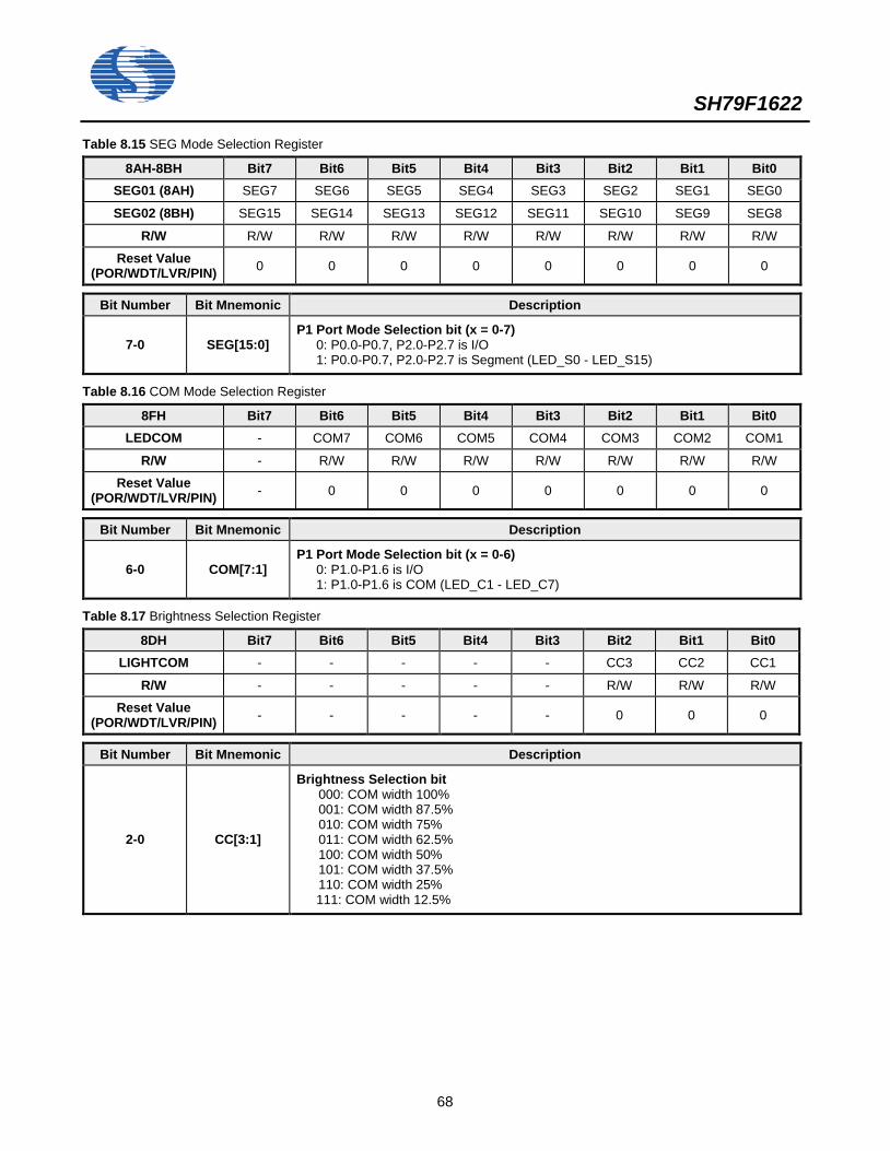
SH79F1622
68
Table 8.15 SEG Mode Selection Register
8AH-8BH Bit7 Bit6 Bit5 Bit4 Bit3 Bit2 Bit1 Bit0 SEG01 (8AH) SEG7 SEG6 SEG5 SEG4 SEG3 SEG2 SEG1 SEG0
SEG02 (8BH) SEG15 SEG14 SEG13 SEG12 SEG11 SEG10 SEG9 SEG8
R/W R/W R/W R/W R/W R/W R/W R/W R/W
Reset Value (POR/WDT/LVR/PIN) 0 0 0 0 0 0 0 0
Bit Number Bit Mnemonic Description
7-0 SEG[15:0] P1 Port Mode Selection bit (x = 0-7)
0: P0.0-P0.7, P2.0-P2.7 is I/O 1: P0.0-P0.7, P2.0-P2.7 is Segment (LED_S0 - LED_S15)
Table 8.16 COM Mode Selection Register
8FH Bit7 Bit6 Bit5 Bit4 Bit3 Bit2 Bit1 Bit0 LEDCOM - COM7 COM6 COM5 COM4 COM3 COM2 COM1
R/W - R/W R/W R/W R/W R/W R/W R/W
Reset Value (POR/WDT/LVR/PIN) - 0 0 0 0 0 0 0
Bit Number Bit Mnemonic Description
6-0 COM[7:1] P1 Port Mode Selection bit (x = 0-6)
0: P1.0-P1.6 is I/O 1: P1.0-P1.6 is COM (LED_C1 - LED_C7)
Table 8.17 Brightness Selection Register
8DH Bit7 Bit6 Bit5 Bit4 Bit3 Bit2 Bit1 Bit0 LIGHTCOM - - - - - CC3 CC2 CC1
R/W - - - - - R/W R/W R/W
Reset Value (POR/WDT/LVR/PIN) - - - - - 0 0 0
Bit Number Bit Mnemonic Description
2-0 CC[3:1]
Brightness Selection bit 000: COM width 100% 001: COM width 87.5% 010: COM width 75% 011: COM width 62.5% 100: COM width 50% 101: COM width 37.5% 110: COM width 25% 111: COM width 12.5%
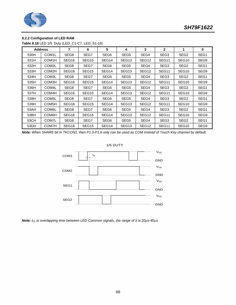
SH79F1622
69
8.2.2 Configuration of LED RAM Table 8.18 LED 1/5 Duty (LED_C1-C7, LED_S1-16)
Address 7 6 5 4 3 2 1 0 530H COM1L SEG8 SEG7 SEG6 SEG5 SEG4 SEG3 SEG2 SEG1 531H COM1H SEG16 SEG15 SEG14 SEG13 SEG12 SEG11 SEG10 SEG9 532H COM2L SEG8 SEG7 SEG6 SEG5 SEG4 SEG3 SEG2 SEG1 533H COM2H SEG16 SEG15 SEG14 SEG13 SEG12 SEG11 SEG10 SEG9 534H COM3L SEG8 SEG7 SEG6 SEG5 SEG4 SEG3 SEG2 SEG1 535H COM3H SEG16 SEG15 SEG14 SEG13 SEG12 SEG11 SEG10 SEG9 536H COM4L SEG8 SEG7 SEG6 SEG5 SEG4 SEG3 SEG2 SEG1 537H COM4H SEG16 SEG15 SEG14 SEG13 SEG12 SEG11 SEG10 SEG9 538H COM5L SEG8 SEG7 SEG6 SEG5 SEG4 SEG3 SEG2 SEG1 539H COM5H SEG16 SEG15 SEG14 SEG13 SEG12 SEG11 SEG10 SEG9 53AH COM6L SEG8 SEG7 SEG6 SEG5 SEG4 SEG3 SEG2 SEG1 53BH COM6H SEG16 SEG15 SEG14 SEG13 SEG12 SEG11 SEG10 SEG9 53CH COM7L SEG8 SEG7 SEG6 SEG5 SEG4 SEG3 SEG2 SEG1 53DH COM7H SEG16 SEG15 SEG14 SEG13 SEG12 SEG11 SEG10 SEG9
Note: When SHARE bit in TKCON1, then P1.0-P1.6 only can be used as COM instead of Touch Key channel by default.
VDD
GND
1/5 DUTY
COM1
SEG1GND
VDD
tol
COM2VDD
GND
SEG2GND
VDD
Note: tOL is overlapping time between LED Common signals, the range of it is 20µs-40µs.
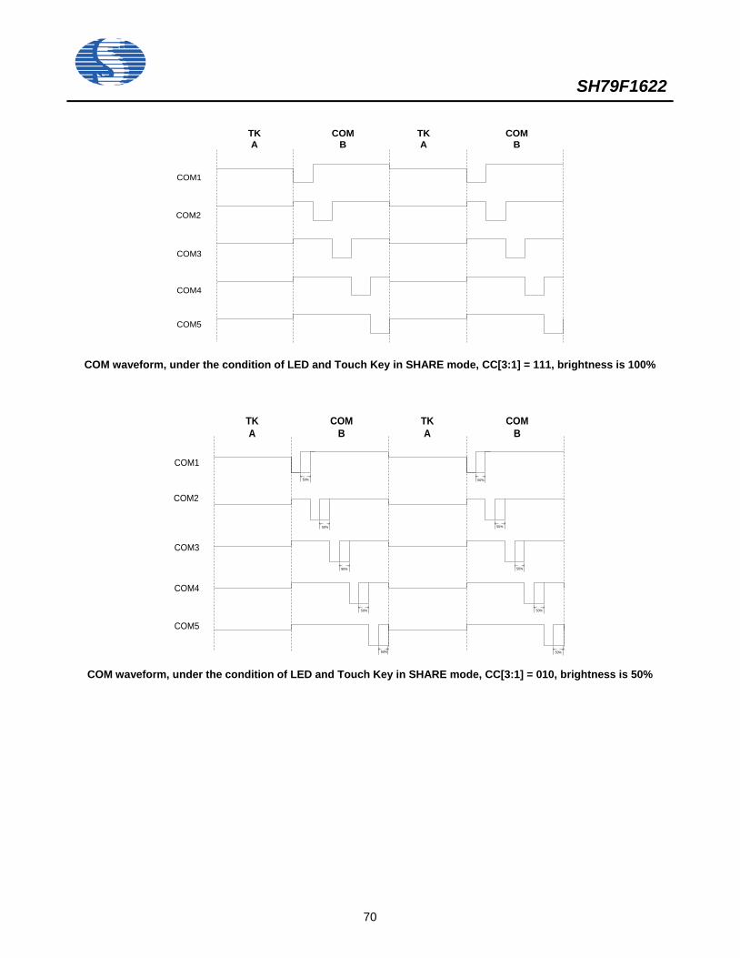
SH79F1622
70
COM
BTKA
COM1
COM2
COM3
COM4
COMB
TKA
COM5
COM waveform, under the condition of LED and Touch Key in SHARE mode, CC[3:1] = 111, brightness is 100%
COMB
TKA
COM1
COM2
COM3
COM4
COMB
TKA
COM5
50%
50%
50%
50%
50%
50%
50%
50%
50%
50% COM waveform, under the condition of LED and Touch Key in SHARE mode, CC[3:1] = 010, brightness is 50%
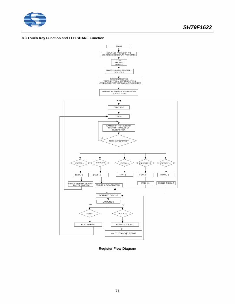
SH79F1622
71
8.3 Touch Key Function and LED SHARE Function
CHOSE CHANNELS REGISTER :TKU1~TKU3
FUNCTION REGISTER:VREF[0:1] ,VTK[0:1] ,CMPD[0:1] ,VTK[0:1]
,RANDOM[0:1] ,TKST[0:7],FSW[0:1],TKRANDOM[0:7]
28Bit AMPLIFICATION FACTOR REGISTER:TKDIV01~TKDIV04
TKGO=1
DELAY 10uS
TKCON = 1SHARE=1LEDON=1
TOUCH KEY INTERRUPT
WATING FOR THE TOUCH-KEYINTERRUPT PRODUCE OR
SCANNING TKIF.
NO
SETUP LED FREQUENCY ANDLIGHTENESS AND DISPLAY PROPERTIES
START
READ 16 Bit DATA REGISTER
SCAN LED COM1~7
IFLED =1 IFTKVO=1
WATIT COUNT0[0:7] TIME
IFlLED =0,TKIF=0 IFTKVO=0,TKIF=0
GO/DONE=1
YES NO
IF IFGO =1
IFGO
IF IFCOUNT =1
IFGO = 0
MINISH Cx
IF IFERR =1
IFERR= 0
CHANGE 28Bit AMPLIFICATIONFACTOR REGISTER
IF IFAVE=1
IFAVE = 0 = 0
IF IFTKOV =1
IFTKOV = 0
CHANGE TKCOUNT
Register Flow Diagram
SH79F1622
72
8.3.1 Function Description SH79F1622 built-in Touch Key function module, which can connect at most 20 keys. When enable LED SHARE function, Touch Key function can connect at most 16 keys. COM1-COM7 is used as LED COM. It is need to notice that, if SHARE function is enable, LED scan function will enable after Touch Key function fininsh data storage.When scanning COM1-COM7 is finished, Touch Key function will restart automatically to start a new key scan and LED. The startup step of Touch Key: (1) Set LED: SEG01-02 = 0FFH, LEDCOM = 7FH, set LED display RAM (2) Set scan frequency of LED, set LED brightness and duty (3) Set TKCON bit, enable Touch Key module (4) Set on-off frequency, reference voltage (Vref), output voltage (OP), key sampling times, key scan sequence, clock width of
key scan, enable touch key & LED share function: FSW[0:1], VREF[0:1], CMPD[0:1], VTK[0;1], TKU1-TKU3, SHARE = 1, LEDON = 1.
(5) Set 28-bit amplification coefficient register: DIV01-04. (6) Software delay 10uS. (7) Set TKGO/D
----
O----
N----
E----
bit, start key scan; Program query interrupt flag bit, TKGO is cleared by hardware. Interrupt flag bit: IFERR,IFGO,IFAVE,IFLED, IFTKOV If IFAVE = 1, reading data register 500H-527H, program save data result, goto step9; If IFERR = 1, data register arithmetic overflow error, clear IFERR and flag bit, reset ting the value of amplification coefficient register, reducing amplification coefficient, go back to step6 to restart scan; If IFGO = 1, key controller start error, clear IFGO and flag bit, go back to step7 to restart scan; If IFCOUNT = 1, key scan count overflow error, clear IFCOUNT and flag bit, reduce CX capacitor or reduce average times.Go back to step7 to restart scan. Interrupt generate (If TKIE = 1), or program query interrupt flag bit, TKGO is cleared by hardware.
(8) Touch Key function module: When scanning Touch Key function is finished, IFTKOV = 0, after key clock width time is finished, goto step9; When scanning Touch Key function is not finished, IFTKOV = 1, after scanning key is finished, goto step9.
(9) Enable LED scan module: Begin to scan COM1-COM7. Program query register, clear TKGO/D
----
O----
N----
E----
bit, then Touch Key scan is finished, program read key data in RAM to judge. Program juage whether touch key to judge interrupt flag bit. If no error flag, go back to step7.
TOUCHKEY Working Mode Table TOUCHKEY and LED can be divided into 3 working mode, according to whether SHARE, shown in the following Table:
TKCON LED_ON SHARE Working Mode 1 0 0 TOUCHKEY work independently 1 1 0 TOUCHKEY and LED work separately 1 0 1 TOUCHKEY and LED are in SHARE mode, LED doesn’t work 1 1 1 TOUCHKEY and LED are in SHARE mode, LED work 0 1 X LED work independently 0 0 X TOUCHKEY and LED don’t work
8.3.2 SHARE Table of SEG Port The control signal of SEG port as shown in the following Table:
TKCON LED_ON SHARE TK_STA 0:TK, 1:LED PXSS SEGX PX
1 X 0 X 0 0 I/O 1 X 0 X 0 1 LED 1 X 0 X 1 X TK 0 X X X 0 0 I/O 0 X X X 0 1 LED 0 X X X 1 X TK 1 X 1 0 0 X I/O 1 X 1 0 1 X TK 1 X 1 1 X 0 I/O 1 X 1 1 X 1 LED
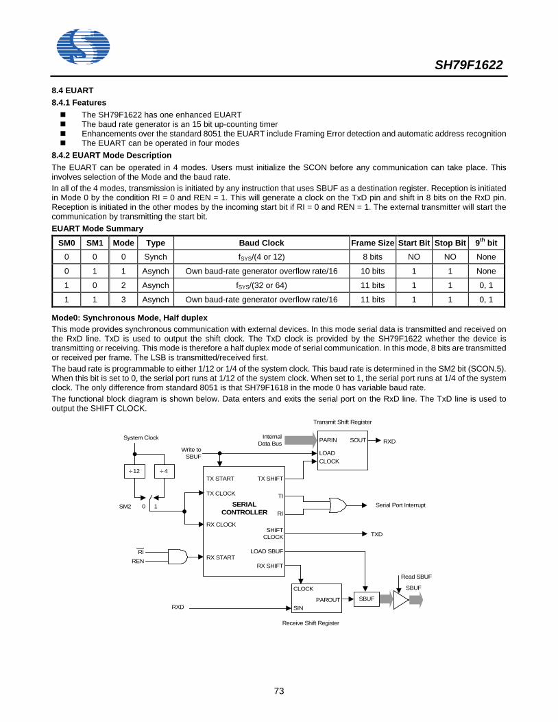
SH79F1622
73
8.4 EUART 8.4.1 Features The SH79F1622 has one enhanced EUART The baud rate generator is an 15 bit up-counting timer Enhancements over the standard 8051 the EUART include Framing Error detection and automatic address recognition The EUART can be operated in four modes
8.4.2 EUART Mode Description The EUART can be operated in 4 modes. Users must initialize the SCON before any communication can take place. This involves selection of the Mode and the baud rate. In all of the 4 modes, transmission is initiated by any instruction that uses SBUF as a destination register. Reception is initiated in Mode 0 by the condition RI = 0 and REN = 1. This will generate a clock on the TxD pin and shift in 8 bits on the RxD pin. Reception is initiated in the other modes by the incoming start bit if RI = 0 and REN = 1. The external transmitter will start the communication by transmitting the start bit. EUART Mode Summary
SM0 SM1 Mode Type Baud Clock Frame Size Start Bit Stop Bit 9th bit 0 0 0 Synch fSYS/(4 or 12) 8 bits NO NO None
0 1 1 Asynch Own baud-rate generator overflow rate/16 10 bits 1 1 None
1 0 2 Asynch fSYS/(32 or 64) 11 bits 1 1 0, 1
1 1 3 Asynch Own baud-rate generator overflow rate/16 11 bits 1 1 0, 1
Mode0: Synchronous Mode, Half duplex This mode provides synchronous communication with external devices. In this mode serial data is transmitted and received on the RxD line. TxD is used to output the shift clock. The TxD clock is provided by the SH79F1622 whether the device is transmitting or receiving. This mode is therefore a half duplex mode of serial communication. In this mode, 8 bits are transmitted or received per frame. The LSB is transmitted/received first. The baud rate is programmable to either 1/12 or 1/4 of the system clock. This baud rate is determined in the SM2 bit (SCON.5). When this bit is set to 0, the serial port runs at 1/12 of the system clock. When set to 1, the serial port runs at 1/4 of the system clock. The only difference from standard 8051 is that SH79F1618 in the mode 0 has variable baud rate. The functional block diagram is shown below. Data enters and exits the serial port on the RxD line. The TxD line is used to output the SHIFT CLOCK.
12 4
SERIALCONTROLLER
TX CLOCK
TX START TX SHIFT
TI
RI
SHIFT CLOCK
RX CLOCK
LOAD SBUFRX START
RX SHIFT
Transmit Shift Register
RXD
Serial Port Interrupt
TXD
RIREN
PARIN
LOADCLOCK
SOUT
CLOCK
SINPAROUT
RXDSBUF
Read SBUF
Receive Shift Register
InternalData Bus
Write to SBUF
10
SBUF
÷ ÷
System Clock
SM2
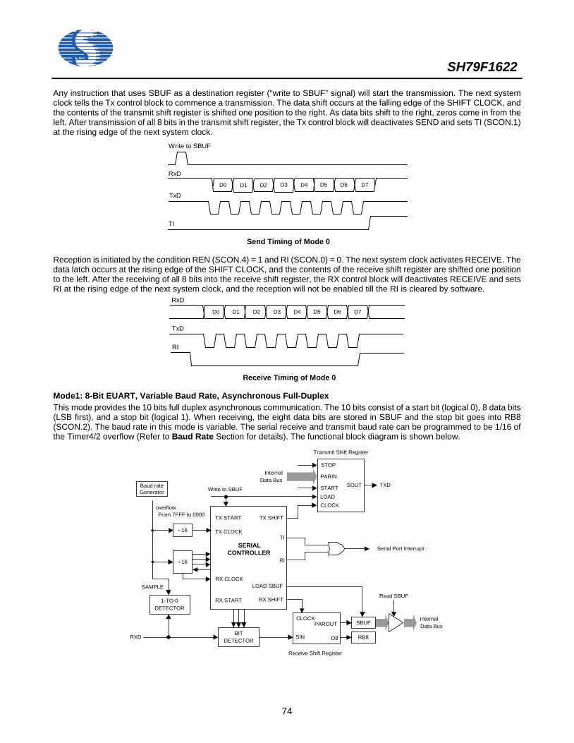
SH79F1622
74
Any instruction that uses SBUF as a destination register (“write to SBUF” signal) will start the transmission. The next system clock tells the Tx control block to commence a transmission. The data shift occurs at the falling edge of the SHIFT CLOCK, and the contents of the transmit shift register is shifted one position to the right. As data bits shift to the right, zeros come in from the left. After transmission of all 8 bits in the transmit shift register, the Tx control block will deactivates SEND and sets TI (SCON.1) at the rising edge of the next system clock.
Write to SBUF
D0 D1 D2 D3 D4 D5 D6 D7
RxD
TI
Send Timing of Mode 0
TxD
Reception is initiated by the condition REN (SCON.4) = 1 and RI (SCON.0) = 0. The next system clock activates RECEIVE. The data latch occurs at the rising edge of the SHIFT CLOCK, and the contents of the receive shift register are shifted one position to the left. After the receiving of all 8 bits into the receive shift register, the RX control block will deactivates RECEIVE and sets RI at the rising edge of the next system clock, and the reception will not be enabled till the RI is cleared by software.
RxD
D0 D1 D2 D3 D4 D5 D6 D7
RI
Receive Timing of Mode 0
TxD
Mode1: 8-Bit EUART, Variable Baud Rate, Asynchronous Full-Duplex This mode provides the 10 bits full duplex asynchronous communication. The 10 bits consist of a start bit (logical 0), 8 data bits (LSB first), and a stop bit (logical 1). When receiving, the eight data bits are stored in SBUF and the stop bit goes into RB8 (SCON.2). The baud rate in this mode is variable. The serial receive and transmit baud rate can be programmed to be 1/16 of the Timer4/2 overflow (Refer to Baud Rate Section for details). The functional block diagram is shown below.
SERIALCONTROLLER
TX CLOCK
TX START TX SHIFT
TI
RI
RX CLOCKLOAD SBUF
RX START RX SHIFT
TXDPARIN
LOADCLOCK
SOUT
CLOCK
SIN
PAROUT
RXD
Read SBUF
InternalData Bus
Receive Shift Register
InternalData Bus
16÷
16÷
1-TO-0DETECTOR
Write to SBUF
BITDETECTOR D8
SBUF
RB8
Transmit Shift Register
STOP
START
SAMPLE
Serial Port Interrupt
Baud rate Generator
overflowFrom 7FFF to 0000
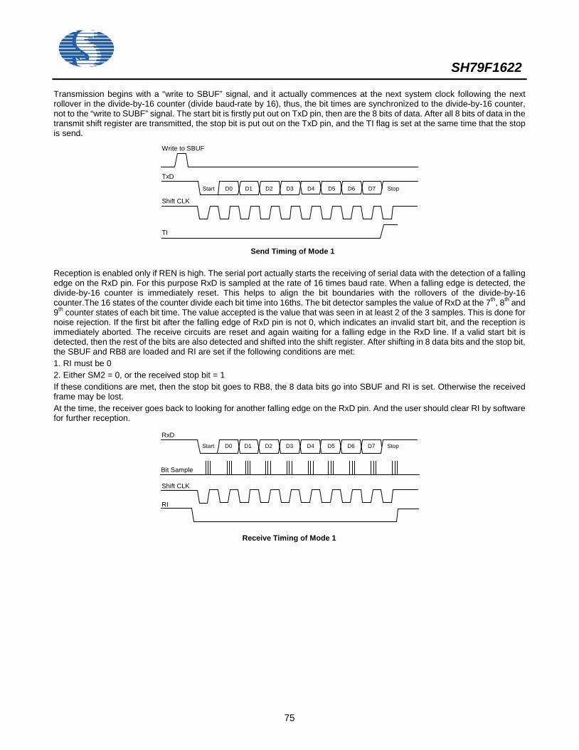
SH79F1622
75
Transmission begins with a “write to SBUF” signal, and it actually commences at the next system clock following the next rollover in the divide-by-16 counter (divide baud-rate by 16), thus, the bit times are synchronized to the divide-by-16 counter, not to the “write to SUBF” signal. The start bit is firstly put out on TxD pin, then are the 8 bits of data. After all 8 bits of data in the transmit shift register are transmitted, the stop bit is put out on the TxD pin, and the TI flag is set at the same time that the stop is send.
Write to SBUF
Shift CLK
D0 D1 D2 D3 D4 D5 D6 D7
TxD
StopStart
TI
Send Timing of Mode 1
Reception is enabled only if REN is high. The serial port actually starts the receiving of serial data with the detection of a falling edge on the RxD pin. For this purpose RxD is sampled at the rate of 16 times baud rate. When a falling edge is detected, the divide-by-16 counter is immediately reset. This helps to align the bit boundaries with the rollovers of the divide-by-16 counter.The 16 states of the counter divide each bit time into 16ths. The bit detector samples the value of RxD at the 7th, 8th and 9th counter states of each bit time. The value accepted is the value that was seen in at least 2 of the 3 samples. This is done for noise rejection. If the first bit after the falling edge of RxD pin is not 0, which indicates an invalid start bit, and the reception is immediately aborted. The receive circuits are reset and again waiting for a falling edge in the RxD line. If a valid start bit is detected, then the rest of the bits are also detected and shifted into the shift register. After shifting in 8 data bits and the stop bit, the SBUF and RB8 are loaded and RI are set if the following conditions are met: 1. RI must be 0 2. Either SM2 = 0, or the received stop bit = 1 If these conditions are met, then the stop bit goes to RB8, the 8 data bits go into SBUF and RI is set. Otherwise the received frame may be lost. At the time, the receiver goes back to looking for another falling edge on the RxD pin. And the user should clear RI by software for further reception.
Receive Timing of Mode 1
D0 D1 D2 D3 D4 D5 D6 D7
RxDStopStart
Bit Sample
Shift CLK
RI
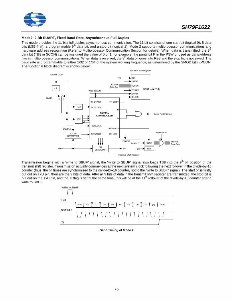
SH79F1622
76
Mode2: 9-Bit EUART, Fixed Baud Rate, Asynchronous Full-Duplex This mode provides the 11 bits full duplex asynchronous communication. The 11 bit consists of one start bit (logical 0), 8 data bits (LSB first), a programmable 9th data bit, and a stop bit (logical 1). Mode 2 supports multiprocessor communications and hardware address recognition (Refer to Multiprocessor Communication Section for details). When data is transmitted, the 9th data bit (TB8 in SCON) can be assigned the value of 0 or 1, for example, the parity bit P in the PSW or used as data/address flag in multiprocessor communications. When data is received, the 9th data bit goes into RB8 and the stop bit is not saved. The baud rate is programmable to either 1/32 or 1/64 of the system working frequency, as determined by the SMOD bit in PCON. The functional block diagram is shown below:
SERIALCONTROLLER
TX CLOCK
TX START TX SHIFT
TI
RI
RX CLOCKLOAD SBUF
RX START RX SHIFT
TXD
Serial Port Interrupt
PARIN
LOADCLOCK
SOUT
CLOCK
SIN
PAROUT
RXD
Read SBUF
InternalData Bus
Receive Shift Register
InternalData Bus
32÷
32÷
1-TO-0DETECTOR
Write to SBUF
BITDETECTOR D8
SBUF
RB8
Transmit Shift Register
STOP
START
SAMPLE
10
2÷
D8TB8
SMOD
System Clock
Transmission begins with a “write to SBUF” signal, the “write to SBUF” signal also loads TB8 into the 9th bit position of the transmit shift register. Transmission actually commences at the next system clock following the next rollover in the divide-by-16 counter (thus, the bit times are synchronized to the divide-by-16 counter, not to the “write to SUBF” signal). The start bit is firstly put out on TxD pin, then are the 9 bits of data. After all 9 bits of data in the transmit shift register are transmitted, the stop bit is put out on the TxD pin, and the TI flag is set at the same time, this will be at the 11th rollover of the divide-by-16 counter after a write to SBUF.
Write to SBUF
Shift CLK
TI
Send Timing of Mode 2
TxD
D8D0 D1 D2 D3 D4 D5 D6 D7Start Stop
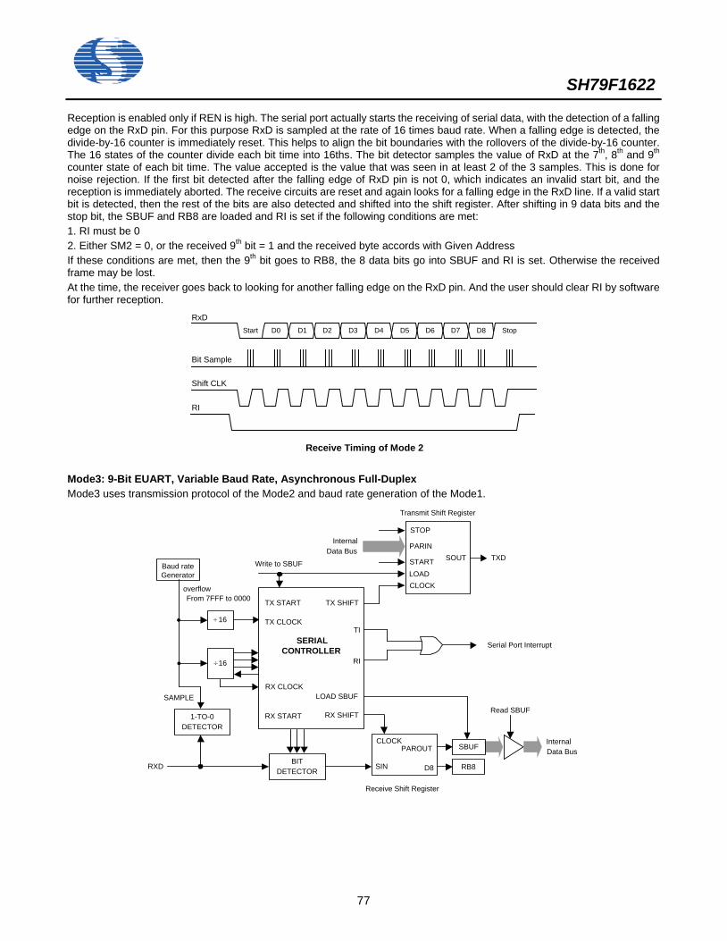
SH79F1622
77
Reception is enabled only if REN is high. The serial port actually starts the receiving of serial data, with the detection of a falling edge on the RxD pin. For this purpose RxD is sampled at the rate of 16 times baud rate. When a falling edge is detected, the divide-by-16 counter is immediately reset. This helps to align the bit boundaries with the rollovers of the divide-by-16 counter. The 16 states of the counter divide each bit time into 16ths. The bit detector samples the value of RxD at the 7th, 8th and 9th counter state of each bit time. The value accepted is the value that was seen in at least 2 of the 3 samples. This is done for noise rejection. If the first bit detected after the falling edge of RxD pin is not 0, which indicates an invalid start bit, and the reception is immediately aborted. The receive circuits are reset and again looks for a falling edge in the RxD line. If a valid start bit is detected, then the rest of the bits are also detected and shifted into the shift register. After shifting in 9 data bits and the stop bit, the SBUF and RB8 are loaded and RI is set if the following conditions are met: 1. RI must be 0 2. Either SM2 = 0, or the received 9th bit = 1 and the received byte accords with Given Address If these conditions are met, then the 9th bit goes to RB8, the 8 data bits go into SBUF and RI is set. Otherwise the received frame may be lost. At the time, the receiver goes back to looking for another falling edge on the RxD pin. And the user should clear RI by software for further reception.
Shift CLK
RxD
Bit Sample
D0 D1 D2 D3 D4 D5 D6 D7 D8Start Stop
RI
Receive Timing of Mode 2
Mode3: 9-Bit EUART, Variable Baud Rate, Asynchronous Full-Duplex Mode3 uses transmission protocol of the Mode2 and baud rate generation of the Mode1.
SERIALCONTROLLER
TX CLOCK
TX START TX SHIFT
TI
RI
RX CLOCKLOAD SBUF
RX START RX SHIFT
TXDPARIN
LOADCLOCK
SOUT
CLOCK
SIN
PAROUT
RXD
Read SBUF
InternalData Bus
Receive Shift Register
InternalData Bus
16÷
16÷
1-TO-0DETECTOR
Write to SBUF
BITDETECTOR D8
SBUF
RB8
Transmit Shift Register
STOP
START
SAMPLE
Serial Port Interrupt
Baud rate Generator
overflowFrom 7FFF to 0000
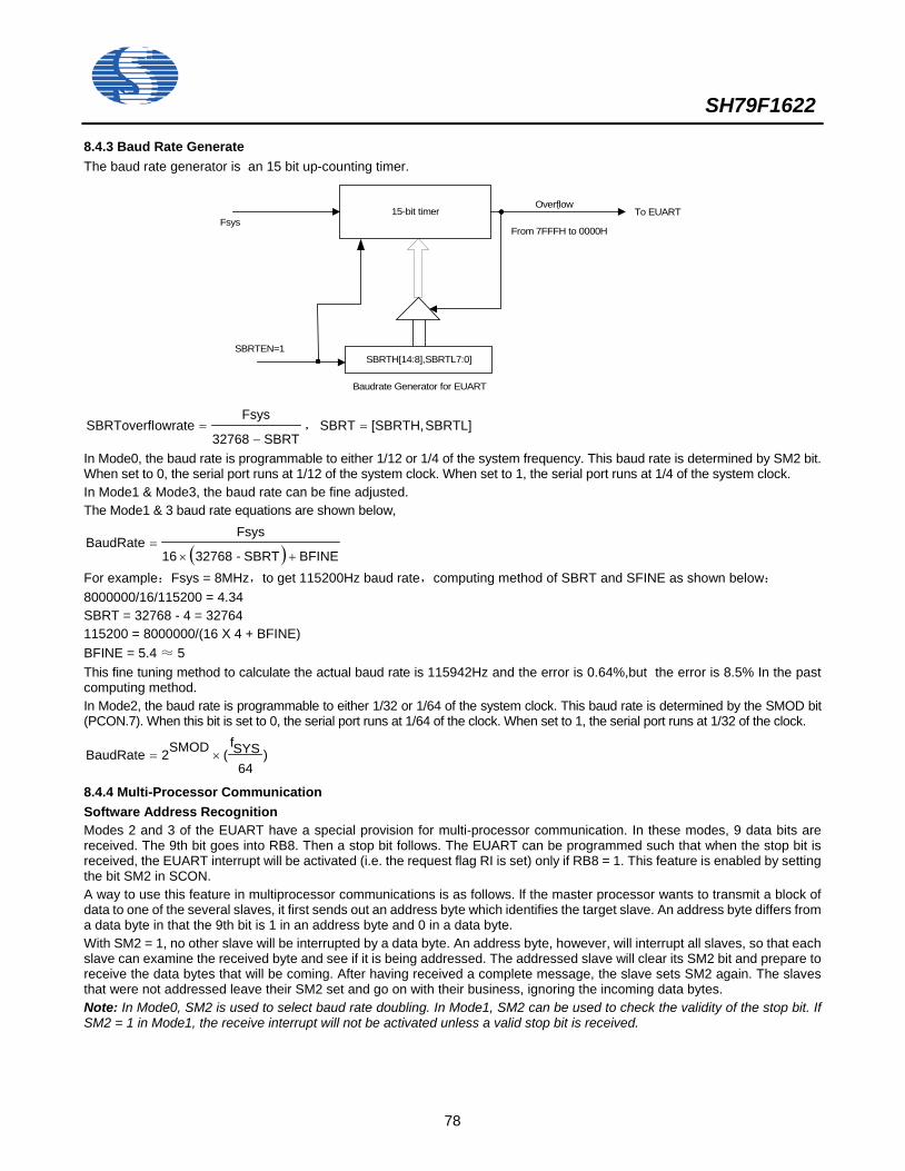
SH79F1622
78
8.4.3 Baud Rate Generate The baud rate generator is an 15 bit up-counting timer.
15-bit timer ` To EUARTOverflow
FsysFrom 7FFFH to 0000H
SBRTH[14:8],SBRTL7:0]
Baudrate Generator for EUART
SBRTEN=1
SBRT32768
FsysowrateSBRToverfl
−= , SBRTL][SBRTH,SBRT =
In Mode0, the baud rate is programmable to either 1/12 or 1/4 of the system frequency. This baud rate is determined by SM2 bit. When set to 0, the serial port runs at 1/12 of the system clock. When set to 1, the serial port runs at 1/4 of the system clock. In Mode1 & Mode3, the baud rate can be fine adjusted. The Mode1 & 3 baud rate equations are shown below,
( ) BFINESBRT-3276816
FsysBaudRate
+×=
For example:Fsys = 8MHz,to get 115200Hz baud rate,computing method of SBRT and SFINE as shown below: 8000000/16/115200 = 4.34 SBRT = 32768 - 4 = 32764 115200 = 8000000/(16 X 4 + BFINE) BFINE = 5.4 ≈ 5 This fine tuning method to calculate the actual baud rate is 115942Hz and the error is 0.64%,but the error is 8.5% In the past computing method. In Mode2, the baud rate is programmable to either 1/32 or 1/64 of the system clock. This baud rate is determined by the SMOD bit (PCON.7). When this bit is set to 0, the serial port runs at 1/64 of the clock. When set to 1, the serial port runs at 1/32 of the clock.
)64
SYSf(SMOD2BaudRate ×=
8.4.4 Multi-Processor Communication Software Address Recognition Modes 2 and 3 of the EUART have a special provision for multi-processor communication. In these modes, 9 data bits are received. The 9th bit goes into RB8. Then a stop bit follows. The EUART can be programmed such that when the stop bit is received, the EUART interrupt will be activated (i.e. the request flag RI is set) only if RB8 = 1. This feature is enabled by setting the bit SM2 in SCON. A way to use this feature in multiprocessor communications is as follows. lf the master processor wants to transmit a block of data to one of the several slaves, it first sends out an address byte which identifies the target slave. An address byte differs from a data byte in that the 9th bit is 1 in an address byte and 0 in a data byte. With SM2 = 1, no other slave will be interrupted by a data byte. An address byte, however, will interrupt all slaves, so that each slave can examine the received byte and see if it is being addressed. The addressed slave will clear its SM2 bit and prepare to receive the data bytes that will be coming. After having received a complete message, the slave sets SM2 again. The slaves that were not addressed leave their SM2 set and go on with their business, ignoring the incoming data bytes. Note: In Mode0, SM2 is used to select baud rate doubling. In Mode1, SM2 can be used to check the validity of the stop bit. If SM2 = 1 in Mode1, the receive interrupt will not be activated unless a valid stop bit is received.
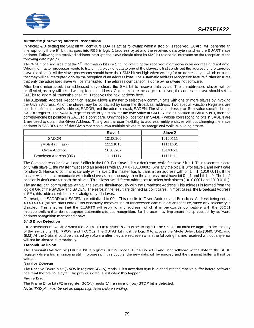
SH79F1622
79
Automatic (Hardware) Address Recognition In Mode2 & 3, setting the SM2 bit will configure EUART act as following: when a stop bit is received, EUART will generate an interrupt only if the 9th bit that goes into RB8 is logic 1 (address byte) and the received data byte matches the EUART slave address. Following the received address interrupt, the slave should clear its SM2 bit to enable interrupts on the reception of the following data byte(s). The 9-bit mode requires that the 9th information bit is a 1 to indicate that the received information is an address and not data. When the master processor wants to transmit a block of data to one of the slaves, it first sends out the address of the targeted slave (or slaves). All the slave processors should have their SM2 bit set high when waiting for an address byte, which ensures that they will be interrupted only by the reception of an address byte. The Automatic address recognition feature further ensures that only the addressed slave will be interrupted. The address comparison is done by hardware not software. After being interrupted, the addressed slave clears the SM2 bit to receive data bytes. The un-addressed slaves will be unaffected, as they will be still waiting for their address. Once the entire message is received, the addressed slave should set its SM2 bit to ignore all transmissions until it receives the next address byte. The Automatic Address Recognition feature allows a master to selectively communicate with one or more slaves by invoking the Given Address. All of the slaves may be contacted by using the Broadcast address. Two special Function Registers are used to define the slave’s address, SADDR, and the address mask, SADEN. The slave address is an 8-bit value specified in the SADDR register. The SADEN register is actually a mask for the byte value in SADDR. If a bit position in SADEN is 0, then the corresponding bit position in SADDR is don’t care. Only those bit positions in SADDR whose corresponding bits in SADEN are 1 are used to obtain the Given Address. This gives the user flexibility to address multiple slaves without changing the slave address in SADDR. Use of the Given Address allows multiple slaves to be recognized while excluding others.
Slave 1 Slave 2 SADDR 10100100 10100111
SADEN (0 mask) 11111010 11111001 Given Address 10100x0x 10100xx1
Broadcast Address (OR) 1111111x 11111111
The Given address for slave 1 and 2 differ in the LSB. For slave 1, it is a don’t care, while for slave 2 it is 1. Thus to communicate only with slave 1, the master must send an address with LSB = 0 (10100000). Similarly the bit 1 is 0 for slave 1 and don’t care for slave 2. Hence to communicate only with slave 2 the master has to transmit an address with bit 1 = 1 (1010 0011). If the master wishes to communicate with both slaves simultaneously, then the address must have bit 0 = 1 and bit 1 = 0. The bit 2 position is don’t care for both the slaves. This allows two different addresses to select both slaves (1010 0001 and 1010 0101). The master can communicate with all the slaves simultaneously with the Broadcast Address. This address is formed from the logical OR of the SADDR and SADEN. The zeros in the result are defined as don’t cares. In most cases, the Broadcast Address is FFh, this address will be acknowledged by all slaves. On reset, the SADDR and SADEN are initialized to 00h. This results in Given Address and Broadcast Address being set as XXXXXXXX (all bits don’t care). This effectively removes the multiprocessor communications feature, since any selectivity is disabled. This ensures that the EUART0 will reply to any address, which it is backwards compatible with the 80C51 microcontrollers that do not support automatic address recognition. So the user may implement multiprocessor by software address recognition mentioned above. 8.4.5 Error Detection Error detection is available when the SSTAT bit in register PCON is set to logic 1.The SSTAT bit must be logic 1 to access any of the status bits (FE, RXOV, and TXCOL). The SSTAT bit must be logic 0 to access the Mode Select bits (SM0, SM1, and SM2).All the 3 bits should be cleared by software after they are set, even when the following frames received without any error will not be cleared automatically. Transmit Collision The Transmit Collision bit (TXCOL bit in register SCON) reads ‘1’ if RI is set 0 and user software writes data to the SBUF register while a transmission is still in progress. If this occurs, the new data will be ignored and the transmit buffer will not be written. Receive Overrun The Receive Overrun bit (RXOV in register SCON) reads ‘1’ if a new data byte is latched into the receive buffer before software has read the previous byte. The previous data is lost when this happen. Frame Error The Frame Error bit (FE in register SCON) reads ‘1’ if an invalid (low) STOP bit is detected. Note: TXD pin must be set as output high level before sending.
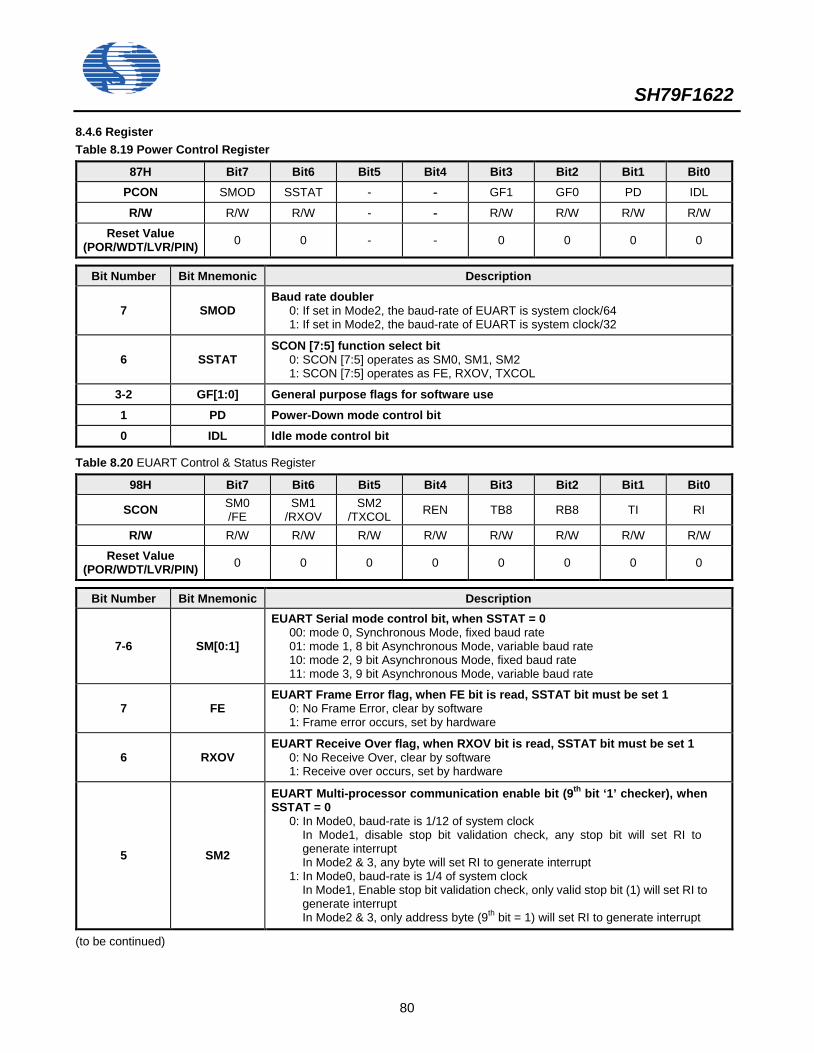
SH79F1622
80
8.4.6 Register Table 8.19 Power Control Register
87H Bit7 Bit6 Bit5 Bit4 Bit3 Bit2 Bit1 Bit0 PCON SMOD SSTAT - - GF1 GF0 PD IDL
R/W R/W R/W - - R/W R/W R/W R/W
Reset Value (POR/WDT/LVR/PIN) 0 0 - - 0 0 0 0
Bit Number Bit Mnemonic Description
7 SMOD Baud rate doubler
0: If set in Mode2, the baud-rate of EUART is system clock/64 1: If set in Mode2, the baud-rate of EUART is system clock/32
6 SSTAT SCON [7:5] function select bit
0: SCON [7:5] operates as SM0, SM1, SM2 1: SCON [7:5] operates as FE, RXOV, TXCOL
3-2 GF[1:0] General purpose flags for software use
1 PD Power-Down mode control bit
0 IDL Idle mode control bit
Table 8.20 EUART Control & Status Register
98H Bit7 Bit6 Bit5 Bit4 Bit3 Bit2 Bit1 Bit0
SCON SM0 /FE
SM1 /RXOV
SM2 /TXCOL REN TB8 RB8 TI RI
R/W R/W R/W R/W R/W R/W R/W R/W R/W
Reset Value (POR/WDT/LVR/PIN) 0 0 0 0 0 0 0 0
Bit Number Bit Mnemonic Description
7-6 SM[0:1]
EUART Serial mode control bit, when SSTAT = 0 00: mode 0, Synchronous Mode, fixed baud rate 01: mode 1, 8 bit Asynchronous Mode, variable baud rate 10: mode 2, 9 bit Asynchronous Mode, fixed baud rate 11: mode 3, 9 bit Asynchronous Mode, variable baud rate
7 FE EUART Frame Error flag, when FE bit is read, SSTAT bit must be set 1
0: No Frame Error, clear by software 1: Frame error occurs, set by hardware
6 RXOV EUART Receive Over flag, when RXOV bit is read, SSTAT bit must be set 1
0: No Receive Over, clear by software 1: Receive over occurs, set by hardware
5 SM2
EUART Multi-processor communication enable bit (9th bit ‘1’ checker), when SSTAT = 0
0: In Mode0, baud-rate is 1/12 of system clock In Mode1, disable stop bit validation check, any stop bit will set RI to generate interrupt In Mode2 & 3, any byte will set RI to generate interrupt
1: In Mode0, baud-rate is 1/4 of system clock In Mode1, Enable stop bit validation check, only valid stop bit (1) will set RI to generate interrupt In Mode2 & 3, only address byte (9th bit = 1) will set RI to generate interrupt
(to be continued)
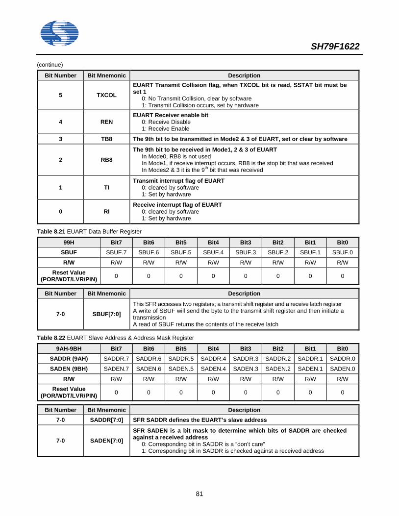
SH79F1622
81
(continue)
Bit Number Bit Mnemonic Description
5 TXCOL EUART Transmit Collision flag, when TXCOL bit is read, SSTAT bit must be set 1
0: No Transmit Collision, clear by software 1: Transmit Collision occurs, set by hardware
4 REN EUART Receiver enable bit
0: Receive Disable 1: Receive Enable
3 TB8 The 9th bit to be transmitted in Mode2 & 3 of EUART, set or clear by software
2 RB8 The 9th bit to be received in Mode1, 2 & 3 of EUART
In Mode0, RB8 is not used In Mode1, if receive interrupt occurs, RB8 is the stop bit that was received In Modes2 & 3 it is the 9th bit that was received
1 TI Transmit interrupt flag of EUART
0: cleared by software 1: Set by hardware
0 RI Receive interrupt flag of EUART
0: cleared by software 1: Set by hardware
Table 8.21 EUART Data Buffer Register
99H Bit7 Bit6 Bit5 Bit4 Bit3 Bit2 Bit1 Bit0 SBUF SBUF.7 SBUF.6 SBUF.5 SBUF.4 SBUF.3 SBUF.2 SBUF.1 SBUF.0
R/W R/W R/W R/W R/W R/W R/W R/W R/W
Reset Value (POR/WDT/LVR/PIN) 0 0 0 0 0 0 0 0
Bit Number Bit Mnemonic Description
7-0 SBUF[7:0] This SFR accesses two registers; a transmit shift register and a receive latch register A write of SBUF will send the byte to the transmit shift register and then initiate a transmission A read of SBUF returns the contents of the receive latch
Table 8.22 EUART Slave Address & Address Mask Register
9AH-9BH Bit7 Bit6 Bit5 Bit4 Bit3 Bit2 Bit1 Bit0 SADDR (9AH) SADDR.7 SADDR.6 SADDR.5 SADDR.4 SADDR.3 SADDR.2 SADDR.1 SADDR.0
SADEN (9BH) SADEN.7 SADEN.6 SADEN.5 SADEN.4 SADEN.3 SADEN.2 SADEN.1 SADEN.0
R/W R/W R/W R/W R/W R/W R/W R/W R/W
Reset Value (POR/WDT/LVR/PIN) 0 0 0 0 0 0 0 0
Bit Number Bit Mnemonic Description 7-0 SADDR[7:0] SFR SADDR defines the EUART’s slave address
7-0 SADEN[7:0] SFR SADEN is a bit mask to determine which bits of SADDR are checked against a received address
0: Corresponding bit in SADDR is a “don’t care” 1: Corresponding bit in SADDR is checked against a received address
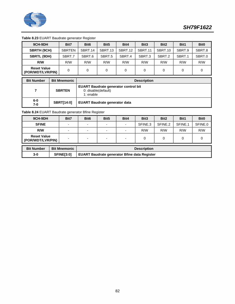
SH79F1622
82
Table 8.23 EUART Baudrate generator Register
9CH-9DH Bit7 Bit6 Bit5 Bit4 Bit3 Bit2 Bit1 Bit0 SBRTH (9CH) SBRTEN SBRT.14 SBRT.13 SBRT.12 SBRT.11 SBRT.10 SBRT.9 SBRT.8
SBRTL (9DH) SBRT.7 SBRT.6 SBRT.5 SBRT.4 SBRT.3 SBRT.2 SBRT.1 SBRT.0
R/W R/W R/W R/W R/W R/W R/W R/W R/W
Reset Value (POR/WDT/LVR/PIN) 0 0 0 0 0 0 0 0
Bit Number Bit Mnemonic Description
7 SBRTEN EUART Baudrate generator control bit
0: disable(default) 1: enable
6-0 7-0 SBRT[14:0] EUART Baudrate generator data
Table 8.24 EUART Baudrate generator Bfine Register
9CH-9DH Bit7 Bit6 Bit5 Bit4 Bit3 Bit2 Bit1 Bit0 SFINE - - - - SFINE.3 SFINE.2 SFINE.1 SFINE.0
R/W - - - - R/W R/W R/W R/W
Reset Value (POR/WDT/LVR/PIN) - - - - 0 0 0 0
Bit Number Bit Mnemonic Description 3-0 SFINE[3:0] EUART Baudrate generator Bfine data Register
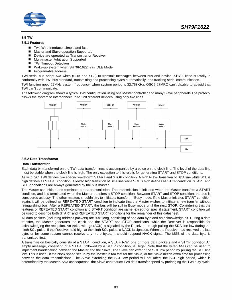
SH79F1622
83
8.5 TWI 8.5.1 Features
Two Wire Interface, simple and fast Master and Slave operation Supported Device are operated as Transmitter or Receiver Multi-master Arbitration Supported TWI Timeout Detection Wake-up system when SH79F1622 is in IDLE Mode Programable address
TWI serial bus adopt two wires (SDA and SCL) to transmit messages between bus and device. SH79F1622 is totally in conformity with TWI bus standard, transmitting and processing bytes automatically, and tracking serial communication. TWI function need 27MHz system frequency, when system period is 32.768KHz, OSC2 27MRC can’t disable to advoid that TWI can’t communicate. The following diagram shows a typical TWI configuration using one Master controller and many Slave peripherals.The protocol allows the system to interconnect up to 128 different devices using only two lines.
SCL
MasterDevice 1
SDA
VDD= 5VVDD= 5V VDD= 5V VDD=5V
SlaveDevice 1
SlaveDevice 2
MasterDevice 2
VDD= 5V
8.5.2 Data Transformat Data Transformat Each data bit transferred on the TWI data transfer lines is accompanied by a pulse on the clock line. The level of the data line must be stable when the clock line is high. The only exception to this rule is for generating START and STOP conditions. As with I2C, TWI defines two special waveform: START and STOP condition. A high to low transition of SDA line while SCL is high defines as START condition; A low to high transition of SDA line while SCL is high defines as STOP condition. START and STOP conditions are always generated by the bus master. The Master can initiate and terminate a data transmission. The transmission is initiated when the Master transfers a START condition, and it is terminated when the Master transfers a STOP condition. Between START and STOP condition, the bus is considered as busy. The other masters shouldn’t try to initiate a transfer. In Busy mode, if the Master initiates START condition again, it will be defined as REPEATED START condition to indicate that the Master wishes to initiate a new transfer without relinquishing bus. After a REPEATED START, the bus will be still in Busy mode until the next STOP. Considering that the features of REPEATED START condition and START condition are same, except for special statement, START condition will be used to describe both START and REPEATED START conditions for the remainder of this datasheet. All data packets (including address packets) are 9-bit long, consisting of one data byte and an acknowledge bit. During a data transfer, the Master generates the clock and the START and STOP conditions, while the Receiver is responsible for acknowledging the reception. An Acknowledge (ACK) is signaled by the Receiver through pulling the SDA line low during the ninth SCL pulse. If the Receiver hold high at the ninth SCL pulse, a NACK is signaled. When the Receiver has received the last byte, or for some reason cannot receive any more bytes, it should respond NACK signal. The MSB of the data byte is transmitted first. A transmission basically consists of a START condition, a SLA + R/W, one or more data packets and a STOP condition.An empty message, consisting of a START followed by a STOP condition, is illegal. Note that the wired-AND can be used to implement handshaking between the Master and the Slave. The Slave can extend the SCL low period by pulling the SCL line low. This is useful if the clock speed set up by the Master is too fast for the Slave, or the Slave needs extra time for processing between the data transmissions. The Slave extending the SCL low period will not affect the SCL high period, which is determined by the Master. As a consequence, the Slave can reduce TWI data transfer speed by prolonging the TWI duty cycle.
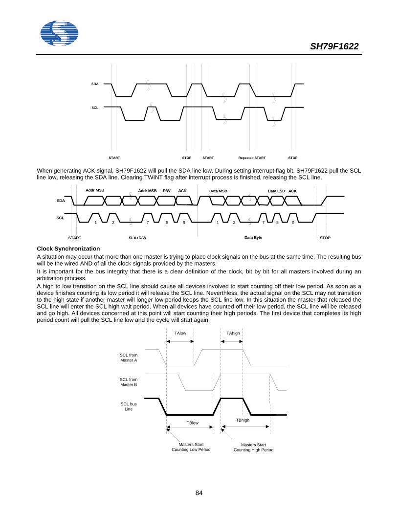
SH79F1622
84
SDA
SCL
START STARTSTOP Repeated START STOP
When generating ACK signal, SH79F1622 will pull the SDA line low. During setting interrupt flag bit, SH79F1622 pull the SCL line low, releasing the SDA line. Clearing TWINT flag after interrupt process is finished, releasing the SCL line.
Addr MSB Addr MSB R/W ACK Data MSB Data LSB ACK
SDA
SCL
START SLA+R/W Data Byte STOP
1 2 7 8 9 1 2 7 8 9
Clock Synchronization A situation may occur that more than one master is trying to place clock signals on the bus at the same time. The resulting bus will be the wired AND of all the clock signals provided by the masters. It is important for the bus integrity that there is a clear definition of the clock, bit by bit for all masters involved during an arbitration process. A high to low transition on the SCL line should cause all devices involved to start counting off their low period. As soon as a device finishes counting its low period it will release the SCL line. Neverthless, the actual signal on the SCL may not transition to the high state if another master will longer low period keeps the SCL line low. In this situation the master that released the SCL line will enter the SCL high wait period. When all devices have counted off their low period, the SCL line will be released and go high. All devices concerned at this point will start counting their high periods. The first device that completes its high period count will pull the SCL line low and the cycle will start again.
SCL fromMaster A
SCL fromMaster B
SCL busLine
Masters StartCounting Low Period
Masters StartCounting High Period
TAlow TAhigh
TBlow TBhigh
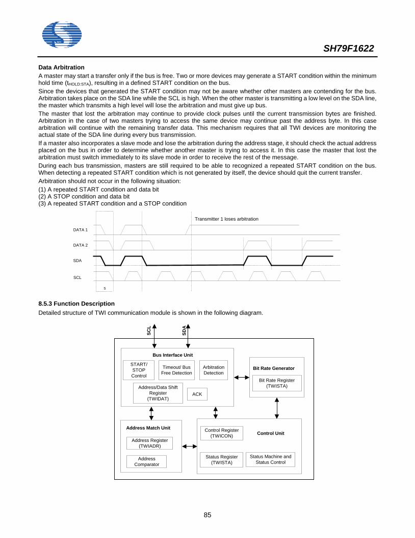
SH79F1622
85
Data Arbitration A master may start a transfer only if the bus is free. Two or more devices may generate a START condition within the minimum hold time (tHOLD:STA), resulting in a defined START condition on the bus. Since the devices that generated the START condition may not be aware whether other masters are contending for the bus. Arbitration takes place on the SDA line while the SCL is high. When the other master is transmitting a low level on the SDA line, the master which transmits a high level will lose the arbitration and must give up bus. The master that lost the arbitration may continue to provide clock pulses until the current transmission bytes are finished. Arbitration in the case of two masters trying to access the same device may continue past the address byte. In this case arbitration will continue with the remaining transfer data. This mechanism requires that all TWI devices are monitoring the actual state of the SDA line during every bus transmission. If a master also incorporates a slave mode and lose the arbitration during the address stage, it should check the actual address placed on the bus in order to determine whether another master is trying to access it. In this case the master that lost the arbitration must switch immediately to its slave mode in order to receive the rest of the message. During each bus transmission, masters are still required to be able to recognized a repeated START condition on the bus. When detecting a repeated START condition which is not generated by itself, the device should quit the current transfer. Arbitration should not occur in the following situation: (1) A repeated START condition and data bit (2) A STOP condition and data bit (3) A repeated START condition and a STOP condition
DATA 1
DATA 2
SDA
SCL
S
Transmitter 1 loses arbitration
8.5.3 Function Description Detailed structure of TWI communication module is shown in the following diagram.
Bit Rate Register(TWISTA)
Address Register(TWIADR)
AddressComparator
Status Register(TWISTA)
Status Machine andStatus Control
Control Register(TWICON)
START/STOPControl
Timeout/ BusFree Detection
ArbitrationDetection
Address/Data ShiftRegister
(TWIDAT)ACK
Bus Interface Unit
Address Match UnitControl Unit
Bit Rate Generator
SCL
SDA
SH79F1622
86
Bus Interface Unit This unit contains the Data and Address Shift Register (TWIDAT), a START/STOP Controller, Arbitration and Timeout detection hardware. The TWIDAT register contains the address or data bytes to be transmitted, or the address or data bytes to be received. The START/STOP Controller is responsible for generation and detection of START, repeated START and STOP conditions. If SH79F1622 has initiated a transmission as Master, the Arbitration Detection hardware continuously monitors the transmission trying to determine if arbitration is in process. If TWI has lost arbitration, the Control Unit is informed Correct action can be taken and appropriate status codes generated. SH79F1622 must hold data stable before SCL from low to high, when SH79F1622 transmit data/address. When SH79F1622 transmit ACK/NACK, SH79F1622 will generate TWINT interrupt after SCL from low to high, and when SCL from high to low, pulling SCL low, releasing SCL when clearing TWINT interrupt. When SH79F1622 transmit ACK/NACK, if TWINT has been cleared and SCL is still high, SDA generates jumping, TWINT interrupt will regenerate, status is 00H. The current communication of SH79F1622 will stop, the process is as the same as general 00H. When SH79F1622 transmit ACK/NACK, if TWINT isn’t cleared and SCL is still high, SDA generates jumping, then the status switch to 00H directly instead of regenerating interrupt. SH79F1622 enter into the status as slave, then the current communication will stop and can generate STA to start master transmission. Or accepting the visit of STA+ADR to own address again. SH79F1622 enter into the status as master, then the current communication will stop and can generate STA to start master transmission. Or accepting the visit of STA+ADR to own address again. After the current communication is terminated, SH79F1622 will don’t take part in the current transmission. If SH779F1622 exists as a master, please enable EFREE function to avoid entering logic deadband. SH79F1622 defines the Bus hold high more than 50us as free mode, releasing the Bus. The function is only used in the transmission process of one packet (8 + 1 bit). When SH79F1622 is in slave transfer mode and the first byte of transferred message is low, the function can be used. STA and RSTA is not situable for this function. If SH79F1622 generates interrupt, TFREE bit in TWICON regiser will be set (if control bit EFREE bit has been set). When SCL line is pulled to low by slave, the communication will be stop temporarily; The master also can’t pull SCL line to high. For solving this problem, TWI defines all devices that take part in transmission pull SCL line to low more than 25ms as Timeout. TOUT bit in TWICON register will be set (if control bit ETOT has been set). TWI module will reset within 10ms and release the Bus. Bit Rate Generator Unit In Master mode, the baud rate si chosen from one of the four clock rates (4KHz, 16KHz, 64KHz, 100KHz (4MHz clock source), setting by CR[1:0] in TWICON register. Address Match Unit The Address Match unit checks if received address bytes match the 7bit address in the address register TWIADR. If the TWI General Call Recognition Enable bit is set, it will check whether match the general address 00H. Upon matching the address, the control unit will generate a appropriate action and corresponding status code. Control Unit The Control Unit monitors the TWI bus and generates corresponding response according to the setting of TWICON register. When an event which requires the attention of the application occurs on the TWI bus, the interrupt flag of TWI will be set, indicating that the status code of the current event will be written to TWISTA register. The status Register TWISTA only can show the communication status information when generating TWI communication interrupt; In other situations, a status code which is used to represent invalid status code in status register. Before clearing the interrupt, SCL line will hold low level. This allows the application software to complete its tasks before allowing the TWI transmission to continue.
SH79F1622
87
8.5.4 Transmission Mode TWI is a byte-oriented and interrupt based communication bus. Interrupts will be generated by all bus events, like reception of a byte or transmission of a START condition. So the application software can do other oparations during a byte transfer. Note that TWI enable (ENTWI) bit in TWICON, all interrupts enable (EA) bit in IEN0 and ETWI bit will decide together whether generating an interrupt when TWINT bit is set. If ETWI bit or EA bit is not set, the application software must poll the TWINT flag to know whether TWI event occurs. Setting the TWINT bit indicates that a TWI transfer has completed, and it is waiting for the response of the application software. At this moment, the sattus register TWISTA contains the current status. The application software can decide which communication will be transmitted by TWI by TWICON register and TWISTA register. The following section will introduce the four major modes of TWI communication and describe all possible status codes. These figures contain the following abbreviations: S : START condition Rs : REPEATED START condition R : Read bit W : Write bit A : Acknowledge bit Ā : Not acknowledge bit DATA : 8-bit data byte P : STOP condition SLA : Slave Address The circles are used to indicate that the interrupt flag is set. The numbers in the circles show the status code held in theTWISTA, with the least 3 bit masked to zero. Before clearing TWINT, the TWI transfer will be suspended, the application must decide whether to continue or stop the current transfer. For each status code, the required software action and details of the following serial transfer are given. Master Transmitter Mode In the Master Transmitter mode, a number of data bytes are transmitted to a slave receive.In order to enter a Master mode,a START condition must be transmitted, a following SLA + W address packet determines MT has entered. By setting ENTWI and STA in TWICON register, clearing STO and TWINT, the TWI logic will test TWI bus and generate a start condition as soon as the bus becomes free. When a START condition is transmitted, the interrupt (TWINT) will be set, the status register TWISTA is 08H. The interrupt service routine should load TWIDAT with the slave address and the data direction bit (SLA + W). Clearing TWINT flag before start the next transfer. When the slave address and the direction bit have been transmitted and an acknowledgment bit has been received, TWINT will be set, and a number of status codes in TWISTA are possible. There are 18H, 20H and 38H for the master mode, and also 68H, 78H and B0H for the slave mode.
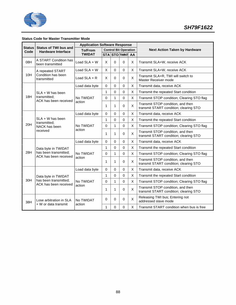
SH79F1622
88
Status Code for Master Transmitter Mode
Status Code
Status of TWI bus and Hardware Interface
Application Software Response Next Action Taken by Hardware To/From
TWIDAT Control Bit Operation STA STO TWINT AA
08H A START Condition has been transmitted Load SLA + W X 0 0 X Transmit SLA+W, receive ACK
10H A repeated START Condition has been transmitted
Load SLA + W X 0 0 X Transmit SLA+W, receive ACK
Load SLA + R X 0 0 X Transmit SLA+R, TWI will switch to Master Receiver mode
18H SLA + W has been transmitted; ACK has been received
Load data byte 0 0 0 X Transmit data, receive ACK
No TWIDAT action
1 0 0 X Transmit the repeated Start condition
0 1 0 X Transmit STOP condition; Clearing STO flag
1 1 0 X Transmit STOP condition, and then transmit START condition; clearing STO
20H
SLA + W has been transmitted; NACK has been received
Load data byte 0 0 0 X Transmit data, receive ACK
No TWIDAT action
1 0 0 X Transmit the repeated Start condition
0 1 0 X Transmit STOP condition; Clearing STO flag
1 1 0 X Transmit STOP condition, and then transmit START condition; clearing STO
28H Data byte in TWIDAT has been transmitted; ACK has been received
Load data byte 0 0 0 X Transmit data, receive ACK
No TWIDAT action
1 0 0 X Transmit the repeated Start condition
0 1 0 X Transmit STOP condition; Clearing STO flag
1 1 0 X Transmit STOP condition, and then transmit START condition; clearing STO
30H Data byte in TWIDAT has been transmitted; ACK has been received
Load data byte 0 0 0 X Transmit data, receive ACK
No TWIDAT action
1 0 0 X Transmit the repeated Start condition
0 1 0 X Transmit STOP condition; Clearing STO flag
1 1 0 X Transmit STOP condition, and then transmit START condition; clearing STO
38H Lose arbitration in SLA + W or data transmit
No TWIDAT action
0 0 0 X Releasing TWI bus; Entering not addressed slave mode
1 0 0 X Transmit START condition when bus is free
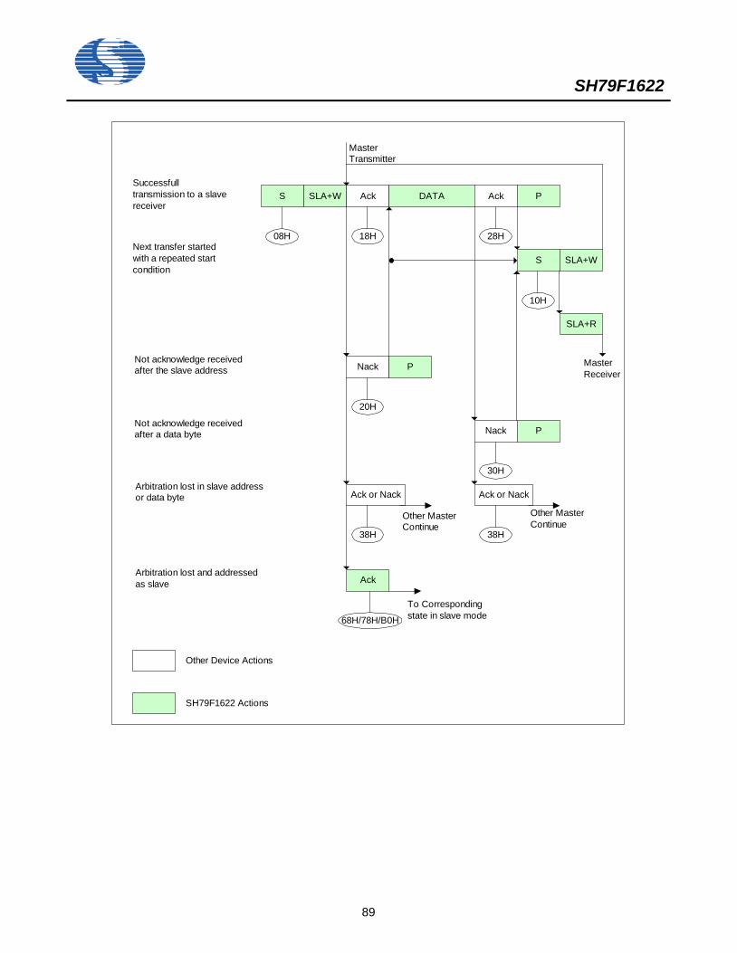
SH79F1622
89
S SLA+W Ack DATA Ack P
S SLA+W
SLA+R
Nack P
Nack P
Ack or Nack Ack or Nack
Ack
Successfulltransmission to a slavereceiver
Next transfer startedwith a repeated startcondition
Not acknowledge receivedafter the slave address
Not acknowledge receivedafter a data byte
Arbitration lost in slave addressor data byte
Arbitration lost and addressedas slave
Other MasterContinue
Other MasterContinue
To Correspondingstate in slave mode
18H 28H
20H
38H
30H
38H
68H/78H/B0H
MasterTransmitter
MasterReceiver
SH79F1622 Actions
Other Device Actions
08H
10H
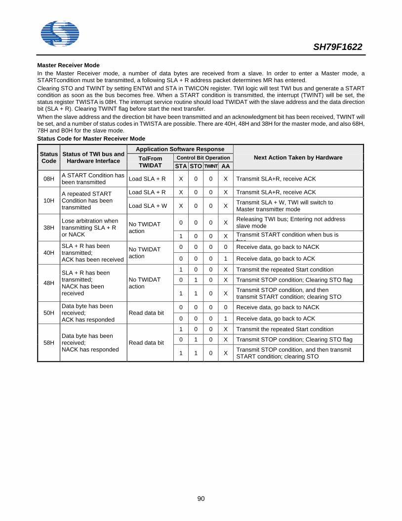
SH79F1622
90
Master Receiver Mode In the Master Receiver mode, a number of data bytes are received from a slave. In order to enter a Master mode, a STARTcondition must be transmitted, a following SLA + R address packet determines MR has entered. Clearing STO and TWINT by setting ENTWI and STA in TWICON register. TWI logic will test TWI bus and generate a START condition as soon as the bus becomes free. When a START condition is transmitted, the interrupt (TWINT) will be set, the status register TWISTA is 08H. The interrupt service routine should load TWIDAT with the slave address and the data direction bit (SLA + R). Clearing TWINT flag before start the next transfer. When the slave address and the direction bit have been transmitted and an acknowledgment bit has been received, TWINT will be set, and a number of status codes in TWISTA are possible. There are 40H, 48H and 38H for the master mode, and also 68H, 78H and B0H for the slave mode. Status Code for Master Receiver Mode
Status Code
Status of TWI bus and Hardware Interface
Application Software Response Next Action Taken by Hardware To/From
TWIDAT Control Bit Operation STA STO TWINT AA
08H A START Condition has been transmitted Load SLA + R X 0 0 X Transmit SLA+R, receive ACK
10H A repeated START Condition has been transmitted
Load SLA + R X 0 0 X Transmit SLA+R, receive ACK
Load SLA + W X 0 0 X Transmit SLA + W, TWI will switch to Master transmitter mode
38H Lose arbitration when transmitting SLA + R or NACK
No TWIDAT action
0 0 0 X Releasing TWI bus; Entering not address slave mode
1 0 0 X Transmit START condition when bus is free
40H SLA + R has been transmitted; ACK has been received
No TWIDAT action
0 0 0 0 Receive data, go back to NACK
0 0 0 1 Receive data, go back to ACK
48H
SLA + R has been transmitted; NACK has been received
No TWIDAT action
1 0 0 X Transmit the repeated Start condition
0 1 0 X Transmit STOP condition; Clearing STO flag
1 1 0 X Transmit STOP condition, and then transmit START condition; clearing STO
50H Data byte has been received; ACK has responded
Read data bit 0 0 0 0 Receive data, go back to NACK
0 0 0 1 Receive data, go back to ACK
58H Data byte has been received; NACK has responded
Read data bit
1 0 0 X Transmit the repeated Start condition
0 1 0 X Transmit STOP condition; Clearing STO flag
1 1 0 X Transmit STOP condition, and then transmit START condition; clearing STO
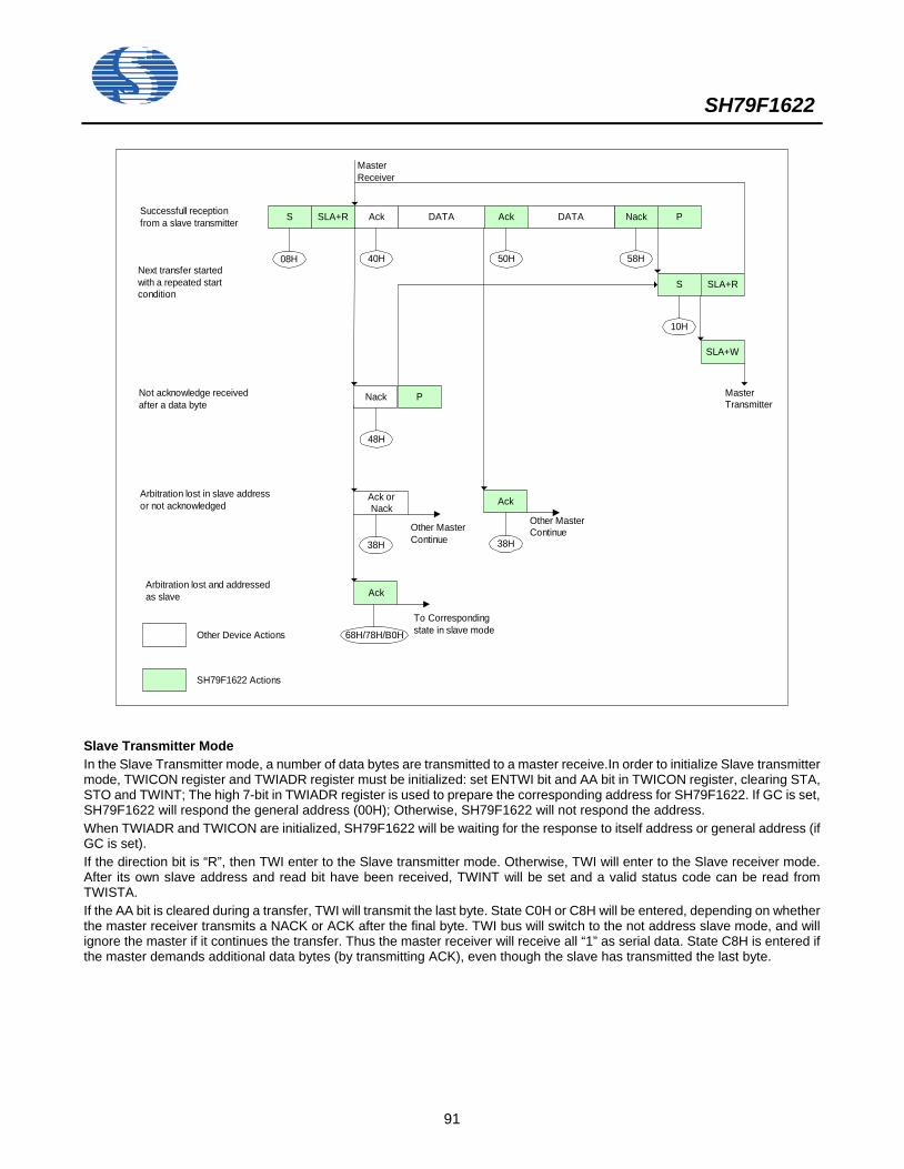
SH79F1622
91
S SLA+R Ack DATA Nack P
S SLA+R
SLA+W
Nack P
Ack orNack
Ack
Ack
Next transfer startedwith a repeated startcondition
Not acknowledge receivedafter a data byte
Arbitration lost in slave addressor not acknowledged
Arbitration lost and addressedas slave
Other MasterContinue
Other MasterContinue
To Correspondingstate in slave mode
40H 58H
48H
38H 38H
68H/78H/B0H
MasterReceiver
MasterTransmitter
Ack DATA
50H
SH79F1622 Actions
Other Device Actions
Successfull receptionfrom a slave transmitter
08H
10H
Slave Transmitter Mode In the Slave Transmitter mode, a number of data bytes are transmitted to a master receive.In order to initialize Slave transmitter mode, TWICON register and TWIADR register must be initialized: set ENTWI bit and AA bit in TWICON register, clearing STA, STO and TWINT; The high 7-bit in TWIADR register is used to prepare the corresponding address for SH79F1622. If GC is set, SH79F1622 will respond the general address (00H); Otherwise, SH79F1622 will not respond the address. When TWIADR and TWICON are initialized, SH79F1622 will be waiting for the response to itself address or general address (if GC is set). If the direction bit is “R”, then TWI enter to the Slave transmitter mode. Otherwise, TWI will enter to the Slave receiver mode. After its own slave address and read bit have been received, TWINT will be set and a valid status code can be read from TWISTA. If the AA bit is cleared during a transfer, TWI will transmit the last byte. State C0H or C8H will be entered, depending on whether the master receiver transmits a NACK or ACK after the final byte. TWI bus will switch to the not address slave mode, and will ignore the master if it continues the transfer. Thus the master receiver will receive all “1” as serial data. State C8H is entered if the master demands additional data bytes (by transmitting ACK), even though the slave has transmitted the last byte.
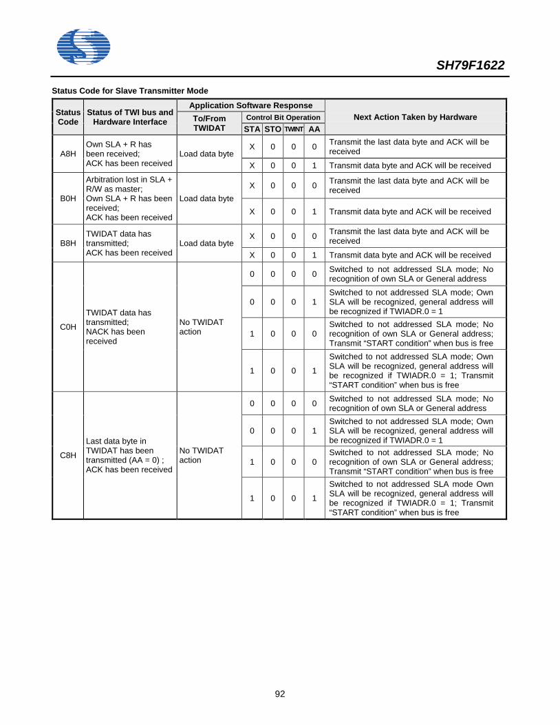
SH79F1622
92
Status Code for Slave Transmitter Mode
Status Code
Status of TWI bus and Hardware Interface
Application Software Response Next Action Taken by Hardware To/From
TWIDAT Control Bit Operation STA STO TWINT AA
A8H Own SLA + R has been received; ACK has been received
Load data byte X 0 0 0 Transmit the last data byte and ACK will be
received
X 0 0 1 Transmit data byte and ACK will be received
B0H
Arbitration lost in SLA + R/W as master; Own SLA + R has been received; ACK has been received
Load data byte X 0 0 0 Transmit the last data byte and ACK will be
received
X 0 0 1 Transmit data byte and ACK will be received
B8H TWIDAT data has transmitted; ACK has been received
Load data byte X 0 0 0 Transmit the last data byte and ACK will be
received
X 0 0 1 Transmit data byte and ACK will be received
C0H
TWIDAT data has transmitted; NACK has been received
No TWIDAT action
0 0 0 0 Switched to not addressed SLA mode; No recognition of own SLA or General address
0 0 0 1 Switched to not addressed SLA mode; Own SLA will be recognized, general address will be recognized if TWIADR.0 = 1
1 0 0 0 Switched to not addressed SLA mode; No recognition of own SLA or General address; Transmit “START condition” when bus is free
1 0 0 1
Switched to not addressed SLA mode; Own SLA will be recognized, general address will be recognized if TWIADR.0 = 1; Transmit “START condition” when bus is free
C8H
Last data byte in TWIDAT has been transmitted (AA = 0) ; ACK has been received
No TWIDAT action
0 0 0 0 Switched to not addressed SLA mode; No recognition of own SLA or General address
0 0 0 1 Switched to not addressed SLA mode; Own SLA will be recognized, general address will be recognized if TWIADR.0 = 1
1 0 0 0 Switched to not addressed SLA mode; No recognition of own SLA or General address; Transmit “START condition” when bus is free
1 0 0 1
Switched to not addressed SLA mode Own SLA will be recognized, general address will be recognized if TWIADR.0 = 1; Transmit “START condition” when bus is free
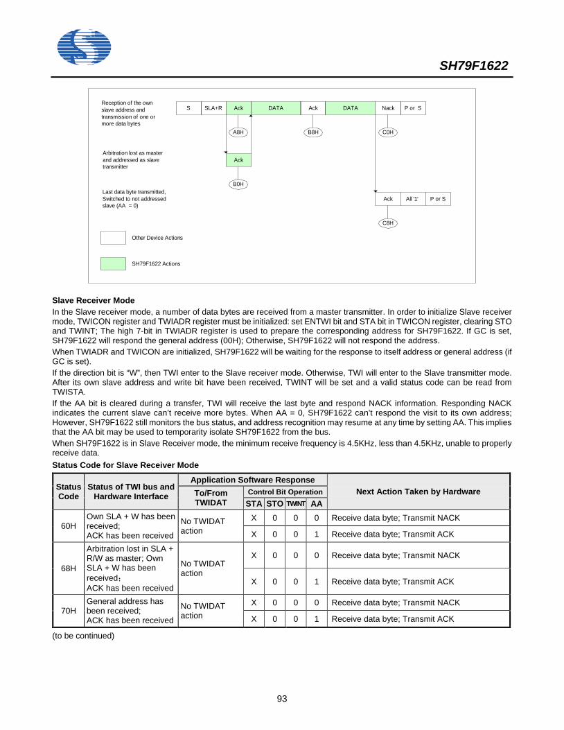
SH79F1622
93
S SLA+R DATA Nack P or S
Ack P or S
Ack
Reception of the ownslave address andtransmission of one ormore data bytes
Arbitration lost as masterand addressed as slavetransmitter
Last data byte transmitted,Switched to not addressedslave (AA = 0)
A8H C0H
B0H
DATA
B8H
SH79F1622 Actions
Other Device Actions
C8H
All '1'
Ack Ack
Slave Receiver Mode In the Slave receiver mode, a number of data bytes are received from a master transmitter. In order to initialize Slave receiver mode, TWICON register and TWIADR register must be initialized: set ENTWI bit and STA bit in TWICON register, clearing STO and TWINT; The high 7-bit in TWIADR register is used to prepare the corresponding address for SH79F1622. If GC is set, SH79F1622 will respond the general address (00H); Otherwise, SH79F1622 will not respond the address. When TWIADR and TWICON are initialized, SH79F1622 will be waiting for the response to itself address or general address (if GC is set). If the direction bit is “W”, then TWI enter to the Slave receiver mode. Otherwise, TWI will enter to the Slave transmitter mode. After its own slave address and write bit have been received, TWINT will be set and a valid status code can be read from TWISTA. If the AA bit is cleared during a transfer, TWI will receive the last byte and respond NACK information. Responding NACK indicates the current slave can’t receive more bytes. When AA = 0, SH79F1622 can’t respond the visit to its own address; However, SH79F1622 still monitors the bus status, and address recognition may resume at any time by setting AA. This implies that the AA bit may be used to temporarity isolate SH79F1622 from the bus. When SH79F1622 is in Slave Receiver mode, the minimum receive frequency is 4.5KHz, less than 4.5KHz, unable to properly receive data. Status Code for Slave Receiver Mode
Status Code
Status of TWI bus and Hardware Interface
Application Software Response Next Action Taken by Hardware To/From
TWIDAT Control Bit Operation STA STO TWINT AA
60H Own SLA + W has been received; ACK has been received
No TWIDAT action
X 0 0 0 Receive data byte; Transmit NACK
X 0 0 1 Receive data byte; Transmit ACK
68H
Arbitration lost in SLA + R/W as master; Own SLA + W has been received; ACK has been received
No TWIDAT action
X 0 0 0 Receive data byte; Transmit NACK
X 0 0 1 Receive data byte; Transmit ACK
70H General address has been received; ACK has been received
No TWIDAT action
X 0 0 0 Receive data byte; Transmit NACK
X 0 0 1 Receive data byte; Transmit ACK
(to be continued)
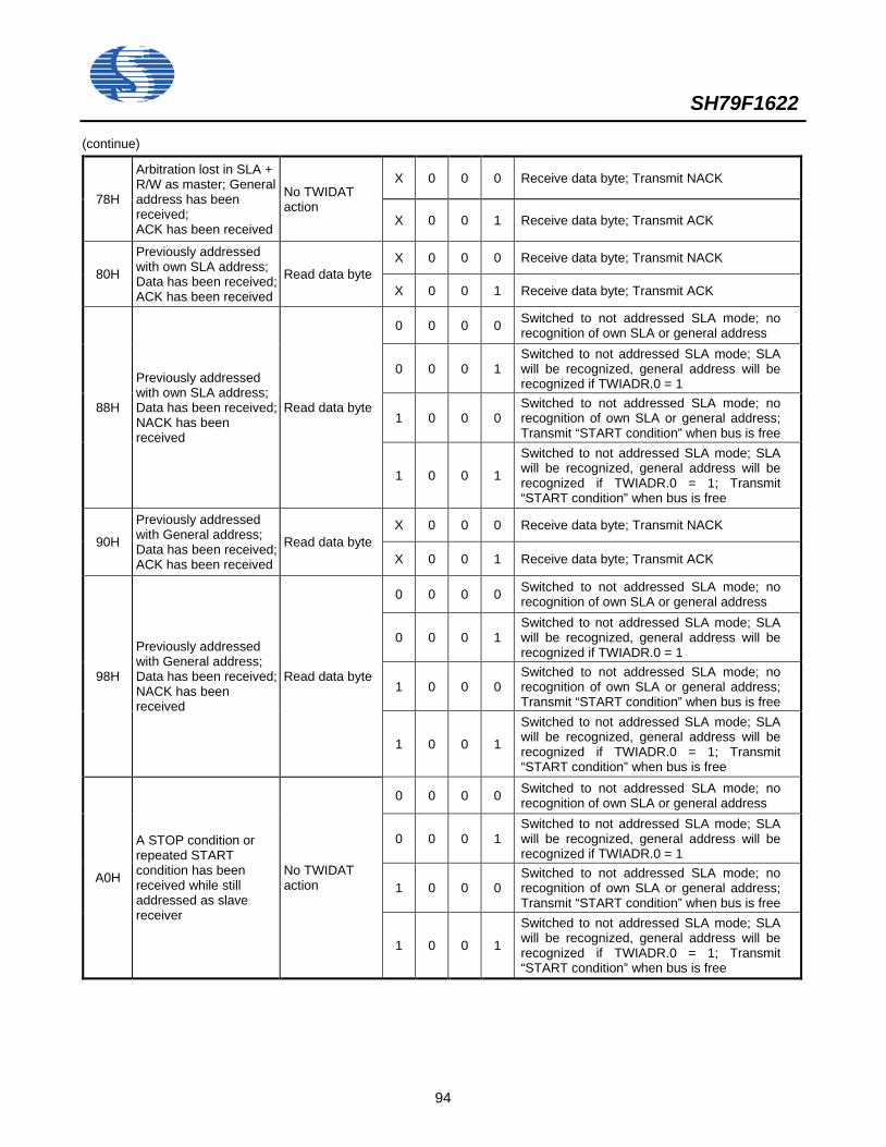
SH79F1622
94
(continue)
78H
Arbitration lost in SLA + R/W as master; General address has been received; ACK has been received
No TWIDAT action
X 0 0 0 Receive data byte; Transmit NACK
X 0 0 1 Receive data byte; Transmit ACK
80H
Previously addressed with own SLA address; Data has been received; ACK has been received
Read data byte X 0 0 0 Receive data byte; Transmit NACK
X 0 0 1 Receive data byte; Transmit ACK
88H
Previously addressed with own SLA address; Data has been received; NACK has been received
Read data byte
0 0 0 0 Switched to not addressed SLA mode; no recognition of own SLA or general address
0 0 0 1 Switched to not addressed SLA mode; SLA will be recognized, general address will be recognized if TWIADR.0 = 1
1 0 0 0 Switched to not addressed SLA mode; no recognition of own SLA or general address; Transmit “START condition” when bus is free
1 0 0 1
Switched to not addressed SLA mode; SLA will be recognized, general address will be recognized if TWIADR.0 = 1; Transmit “START condition” when bus is free
90H
Previously addressed with General address; Data has been received; ACK has been received
Read data byte X 0 0 0 Receive data byte; Transmit NACK
X 0 0 1 Receive data byte; Transmit ACK
98H
Previously addressed with General address; Data has been received; NACK has been received
Read data byte
0 0 0 0 Switched to not addressed SLA mode; no recognition of own SLA or general address
0 0 0 1 Switched to not addressed SLA mode; SLA will be recognized, general address will be recognized if TWIADR.0 = 1
1 0 0 0 Switched to not addressed SLA mode; no recognition of own SLA or general address; Transmit “START condition” when bus is free
1 0 0 1
Switched to not addressed SLA mode; SLA will be recognized, general address will be recognized if TWIADR.0 = 1; Transmit “START condition” when bus is free
A0H
A STOP condition or repeated START condition has been received while still addressed as slave receiver
No TWIDAT action
0 0 0 0 Switched to not addressed SLA mode; no recognition of own SLA or general address
0 0 0 1 Switched to not addressed SLA mode; SLA will be recognized, general address will be recognized if TWIADR.0 = 1
1 0 0 0 Switched to not addressed SLA mode; no recognition of own SLA or general address; Transmit “START condition” when bus is free
1 0 0 1
Switched to not addressed SLA mode; SLA will be recognized, general address will be recognized if TWIADR.0 = 1; Transmit “START condition” when bus is free
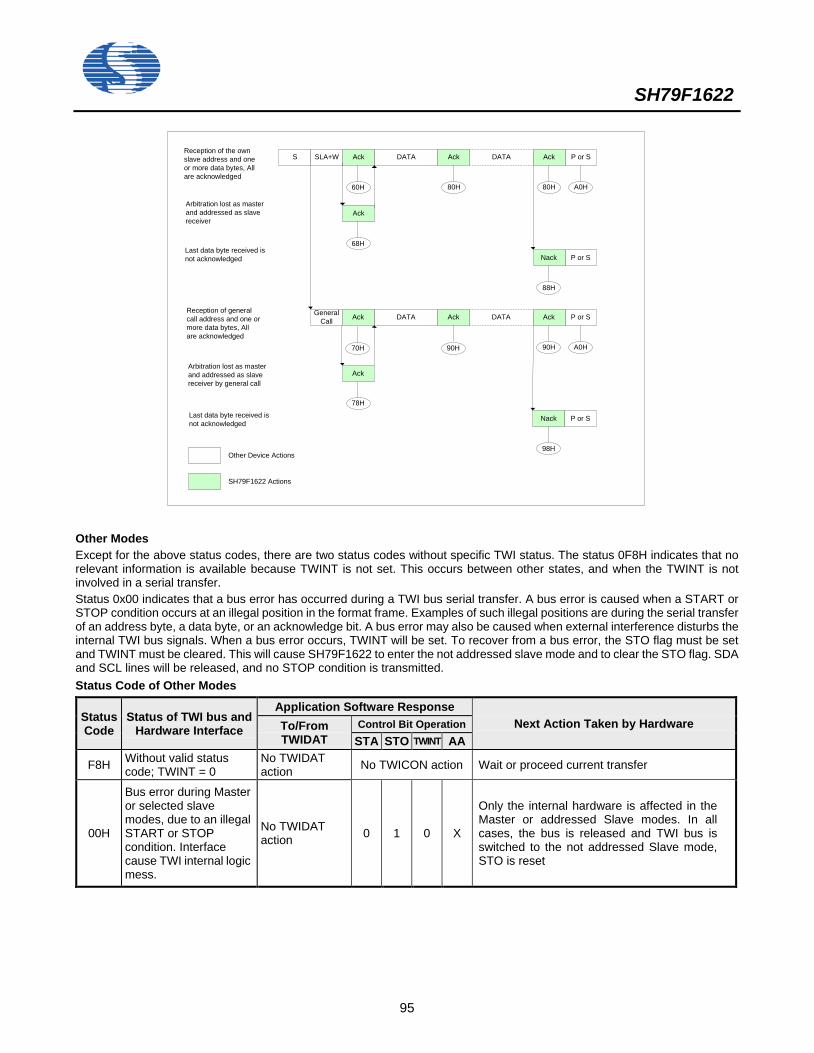
SH79F1622
95
S SLA+W Ack DATA Ack P or S
Nack P or S
Ack
Reception of the own slave address and one or more data bytes, All are acknowledged
Arbitration lost as master and addressed as slave receiver
Last data byte received is not acknowledged
80H
Ack DATA
80H
SH79F1622 Actions
Other Device Actions
88H
A0H
General Call Ack DATA Ack P or S
Nack P or S
Reception of general call address and one or more data bytes, All are acknowledged
Arbitration lost as master and addressed as slave receiver by general call
Last data byte received is not acknowledged
90H
Ack DATA
70H
98H
A0H
68H
60H
78H
90H
Ack
Other Modes Except for the above status codes, there are two status codes without specific TWI status. The status 0F8H indicates that no relevant information is available because TWINT is not set. This occurs between other states, and when the TWINT is not involved in a serial transfer. Status 0x00 indicates that a bus error has occurred during a TWI bus serial transfer. A bus error is caused when a START or STOP condition occurs at an illegal position in the format frame. Examples of such illegal positions are during the serial transfer of an address byte, a data byte, or an acknowledge bit. A bus error may also be caused when external interference disturbs the internal TWI bus signals. When a bus error occurs, TWINT will be set. To recover from a bus error, the STO flag must be set and TWINT must be cleared. This will cause SH79F1622 to enter the not addressed slave mode and to clear the STO flag. SDA and SCL lines will be released, and no STOP condition is transmitted. Status Code of Other Modes
Status Code
Status of TWI bus and Hardware Interface
Application Software Response Next Action Taken by Hardware To/From
TWIDAT Control Bit Operation STA STO TWINT AA
F8H Without valid status code; TWINT = 0
No TWIDAT action No TWICON action Wait or proceed current transfer
00H
Bus error during Master or selected slave modes, due to an illegal START or STOP condition. Interface cause TWI internal logic mess.
No TWIDAT action 0 1 0 X
Only the internal hardware is affected in the Master or addressed Slave modes. In all cases, the bus is released and TWI bus is switched to the not addressed Slave mode, STO is reset
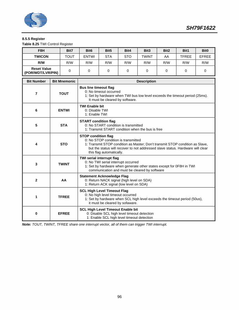
SH79F1622
96
8.5.5 Register Table 8.25 TWI Control Register
F8H Bit7 Bit6 Bit5 Bit4 Bit3 Bit2 Bit1 Bit0 TWICON TOUT ENTWI STA STO TWINT AA TFREE EFREE
R/W R/W R/W R/W R/W R/W R/W R/W R/W
Reset Value (POR/WDT/LVR/PIN) 0 0 0 0 0 0 0 0
Bit Number Bit Mnemonic Description
7 TOUT Bus line timeout flag
0: No timeout occurred 1: Set by hardware when TWI bus low level exceeds the timeout period (25ms).
It must be cleared by software.
6 ENTWI TWI Enable bit
0: Disable TWI 1: Enable TWI
5 STA START condition flag
0: No START condition is transmitted 1: Transmit START condition when the bus is free
4 STO
STOP condition flag 0: No STOP condition is transmitted 1: Transmit STOP condition as Master; Don’t transmit STOP condition as Slave,
but the status will recover to not addressed slave status. Hardware will clear this flag automatically.
3 TWINT TWI serial interrupt flag
0: No TWI serial interrupt occurred 1: Set by hardware when generate other states except for 0F8H in TWI
communication and must be cleared by software
2 AA Statement Acknowledge Flag
0: Return NACK signal (high level on SDA) 1: Return ACK signal (low level on SDA)
1 TFREE SCL High Level Timeout Flag
0: No high level timeout occurred 1: Set by hardware when SCL high level exceeds the timeout period (50us),
it must be cleared by sofaware.
0 EFREE SCL High Level Timeout Enable bit
0: Disable SCL high level timeout detection 1: Enable SCL high level timeout detection
Note: TOUT, TWINT, TFREE share one interrupt vector, all of them can trigger TWI interrupt.
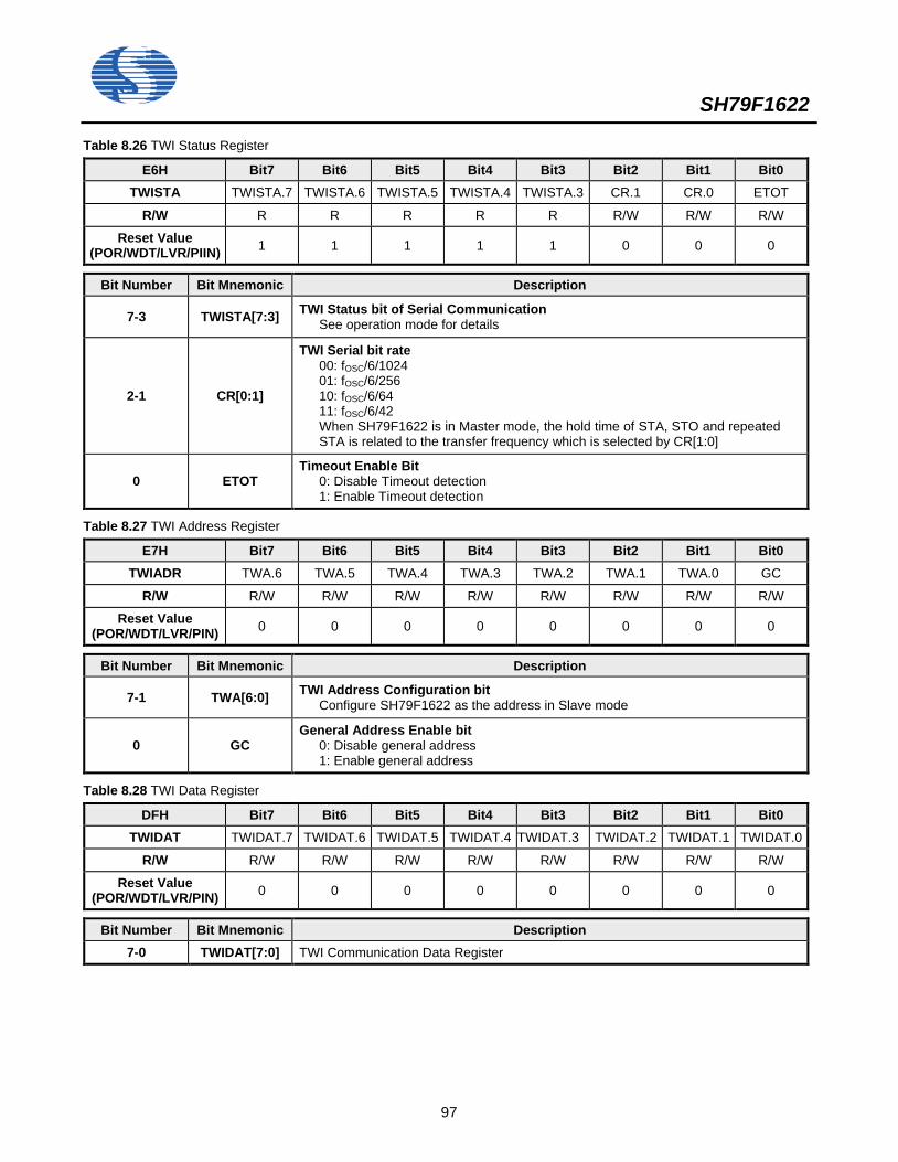
SH79F1622
97
Table 8.26 TWI Status Register
E6H Bit7 Bit6 Bit5 Bit4 Bit3 Bit2 Bit1 Bit0 TWISTA TWISTA.7 TWISTA.6 TWISTA.5 TWISTA.4 TWISTA.3 CR.1 CR.0 ETOT
R/W R R R R R R/W R/W R/W
Reset Value (POR/WDT/LVR/PIIN) 1 1 1 1 1 0 0 0
Bit Number Bit Mnemonic Description
7-3 TWISTA[7:3] TWI Status bit of Serial Communication See operation mode for details
2-1 CR[0:1]
TWI Serial bit rate 00: fOSC/6/1024 01: fOSC/6/256 10: fOSC/6/64 11: fOSC/6/42 When SH79F1622 is in Master mode, the hold time of STA, STO and repeated STA is related to the transfer frequency which is selected by CR[1:0]
0 ETOT Timeout Enable Bit
0: Disable Timeout detection 1: Enable Timeout detection
Table 8.27 TWI Address Register
E7H Bit7 Bit6 Bit5 Bit4 Bit3 Bit2 Bit1 Bit0 TWIADR TWA.6 TWA.5 TWA.4 TWA.3 TWA.2 TWA.1 TWA.0 GC
R/W R/W R/W R/W R/W R/W R/W R/W R/W
Reset Value (POR/WDT/LVR/PIN) 0 0 0 0 0 0 0 0
Bit Number Bit Mnemonic Description
7-1 TWA[6:0] TWI Address Configuration bit Configure SH79F1622 as the address in Slave mode
0 GC General Address Enable bit
0: Disable general address 1: Enable general address
Table 8.28 TWI Data Register
DFH Bit7 Bit6 Bit5 Bit4 Bit3 Bit2 Bit1 Bit0 TWIDAT TWIDAT.7 TWIDAT.6 TWIDAT.5 TWIDAT.4 TWIDAT.3 TWIDAT.2 TWIDAT.1 TWIDAT.0
R/W R/W R/W R/W R/W R/W R/W R/W R/W
Reset Value (POR/WDT/LVR/PIN) 0 0 0 0 0 0 0 0
Bit Number Bit Mnemonic Description 7-0 TWIDAT[7:0] TWI Communication Data Register
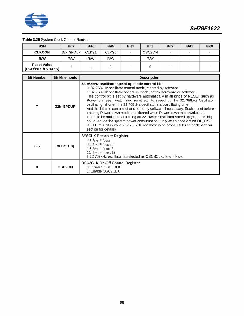
SH79F1622
98
Table 8.29 System Clock Control Register
B2H Bit7 Bit6 Bit5 Bit4 Bit3 Bit2 Bit1 Bit0 CLKCON 32k_SPDUP CLKS1 CLKS0 - OSC2ON - - -
R/W R/W R/W R/W - R/W - - -
Reset Value (POR/WDT/LVR/PIN) 1 1 1 - 0 - - -
Bit Number Bit Mnemonic Description
7 32k_SPDUP
32.768kHz oscillator speed up mode control bit 0: 32.768kHz oscillator normal mode, cleared by software. 1: 32.768kHz oscillator speed up mode, set by hardware or software. This control bit is set by hardware automatically in all kinds of RESET such as Power on reset, watch dog reset etc. to speed up the 32.768kHz Oscillator oscillating, shorten the 32.768kHz oscillator start-oscillating time. And this bit also can be set or cleared by software if necessary. Such as set before entering Power-down mode and cleared when Power-down mode wakes up. It should be noticed that turning off 32.768kHz oscillator speed up (clear this bit) could reduce the system power consumption. Only when code option OP_OSC is 011, this bit is valid. (32.768kHz oscillator is selected, Refer to code option section for details)
6-5 CLKS[1:0]
SYSCLK Prescaler Register 00: fSYS = fOSCS 01: fSYS = fOSCS/2 10: fSYS = fOSCS/4 11: fSYS = fOSCS/12 If 32.768kHz oscillator is selected as OSCSCLK, fSYS = fOSCS
3 OSC2ON OSC2CLK On-Off Control Register
0: Disable OSC2CLK 1: Enable OSC2CLK
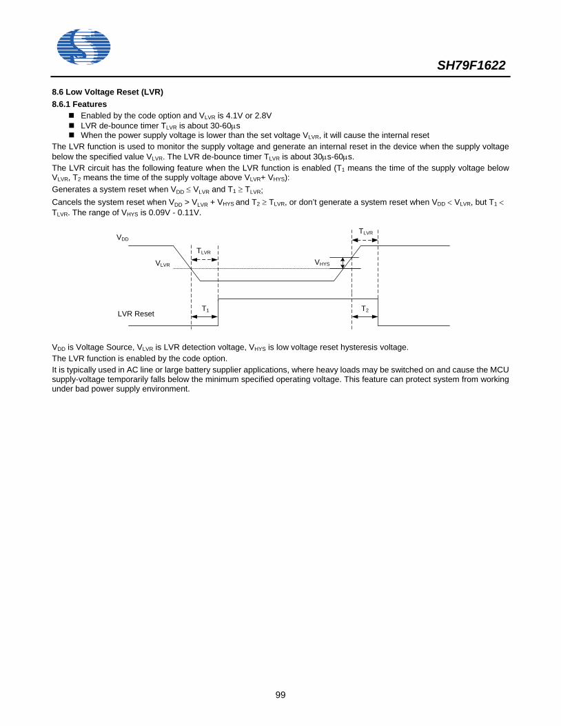
SH79F1622
99
8.6 Low Voltage Reset (LVR) 8.6.1 Features
Enabled by the code option and VLVR is 4.1V or 2.8V LVR de-bounce timer TLVR is about 30-60µs When the power supply voltage is lower than the set voltage VLVR, it will cause the internal reset
The LVR function is used to monitor the supply voltage and generate an internal reset in the device when the supply voltage below the specified value VLVR. The LVR de-bounce timer TLVR is about 30µs-60µs. The LVR circuit has the following feature when the LVR function is enabled (T1 means the time of the supply voltage below VLVR, T2 means the time of the supply voltage above VLVR+ VHYS): Generates a system reset when VDD ≤ VLVR and T1 ≥ TLVR; Cancels the system reset when VDD > VLVR + VHYS and T2 ≥ TLVR, or don’t generate a system reset when VDD < VLVR, but T1 < TLVR. The range of VHYS is 0.09V - 0.11V.
VDD
VLVR
TLVR
TLVR
VHYS
LVR ResetT1 T2
VDD is Voltage Source, VLVR is LVR detection voltage, VHYS is low voltage reset hysteresis voltage. The LVR function is enabled by the code option. It is typically used in AC line or large battery supplier applications, where heavy loads may be switched on and cause the MCU supply-voltage temporarily falls below the minimum specified operating voltage. This feature can protect system from working under bad power supply environment.
SH79F1622
100
8.7 Watchdog Timer (WDT) and Reset State 8.7.1 Features
Auto detect Program Counter (PC) over range, and generate OVL Reset WDT runs even in the Power-Down mode Selectable different WDT overflow frequency
OVL Reset To enhance the anti-noise ability, SH79F1622 built in Program Counter (PC) over range detect circuit, if program counter value is larger than flash romsize, or detect operation code equal to A5H which is not exist in 8051 instruction set, a OVL reset will be generate to reset CPU, and set WDOF bit. So, to make use of this feature, you should fill unused flash rom with A5H. Watchdog Timer The watchdog timer is a down counter, and its clock source is an independent built-in RC oscillator, so it always runs even in the Power-Down mode. The watchdog timer will generate a device reset when it overflows. It can be enabled or disabled permanently by the code option. The watchdog timer control bits (WDT.2-0) are used to select different overflow frequency. The watchdog timer overflow flag (WDOF) will be automatically set to “1” by hardware when overflow happens. To prevent overflow happen, by reading or writing the WDT register RSTSTAT, the watchdog timer should re-count before the overflow happens. There are also some reset flags in this register as below:
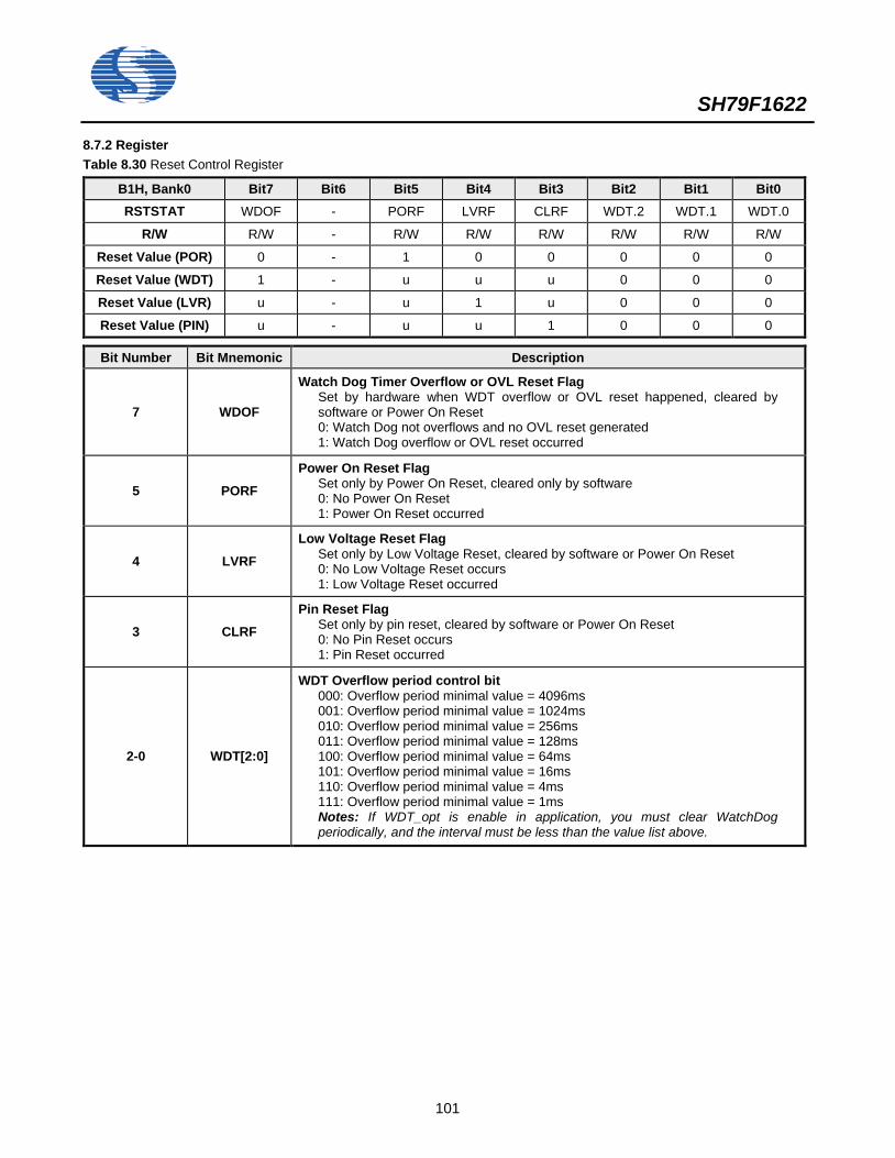
SH79F1622
101
8.7.2 Register Table 8.30 Reset Control Register
B1H, Bank0 Bit7 Bit6 Bit5 Bit4 Bit3 Bit2 Bit1 Bit0 RSTSTAT WDOF - PORF LVRF CLRF WDT.2 WDT.1 WDT.0
R/W R/W - R/W R/W R/W R/W R/W R/W
Reset Value (POR) 0 - 1 0 0 0 0 0
Reset Value (WDT) 1 - u u u 0 0 0
Reset Value (LVR) u - u 1 u 0 0 0
Reset Value (PIN) u - u u 1 0 0 0
Bit Number Bit Mnemonic Description
7 WDOF
Watch Dog Timer Overflow or OVL Reset Flag Set by hardware when WDT overflow or OVL reset happened, cleared by software or Power On Reset 0: Watch Dog not overflows and no OVL reset generated 1: Watch Dog overflow or OVL reset occurred
5 PORF Power On Reset Flag
Set only by Power On Reset, cleared only by software 0: No Power On Reset 1: Power On Reset occurred
4 LVRF Low Voltage Reset Flag
Set only by Low Voltage Reset, cleared by software or Power On Reset 0: No Low Voltage Reset occurs 1: Low Voltage Reset occurred
3 CLRF Pin Reset Flag
Set only by pin reset, cleared by software or Power On Reset 0: No Pin Reset occurs 1: Pin Reset occurred
2-0 WDT[2:0]
WDT Overflow period control bit 000: Overflow period minimal value = 4096ms 001: Overflow period minimal value = 1024ms 010: Overflow period minimal value = 256ms 011: Overflow period minimal value = 128ms 100: Overflow period minimal value = 64ms 101: Overflow period minimal value = 16ms 110: Overflow period minimal value = 4ms 111: Overflow period minimal value = 1ms Notes: If WDT_opt is enable in application, you must clear WatchDog periodically, and the interval must be less than the value list above.
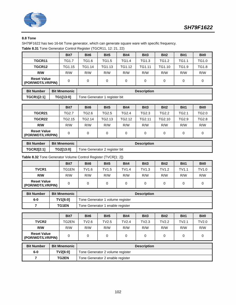
SH79F1622
102
8.8 Tone SH79F1622 has two 16-bit Tone generator, which can generate square ware with specific frequency. Table 8.31 Tone Generator Control Register (TGCR11, 12: 21, 22)
Bit7 Bit6 Bit5 Bit4 Bit3 Bit2 Bit1 Bit0 TGCR11 TG1.7 TG1.6 TG1.5 TG1.4 TG1.3 TG1.2 TG1.1 TG1.0
TGCR12 TG1.15 TG1.14 TG1.13 TG1.12 TG1.11 TG1.10 TG1.9 TG1.8
R/W R/W R/W R/W R/W R/W R/W R/W R/W
Reset Value (POR/WDT/LVR/PIN) 0 0 0 0 0 0 0 0
Bit Number Bit Mnemonic Description TGCR1[2:1] TG1[13:0] Tone Generator 1 register bit
Bit7 Bit6 Bit5 Bit4 Bit3 Bit2 Bit1 Bit0 TGCR21 TG2.7 TG2.6 TG2.5 TG2.4 TG2.3 TG2.2 TG2.1 TG2.0
TGCR22 TG2.15 TG2.14 TG2.13 TG2.12 TG2.11 TG2.10 TG2.9 TG2.8
R/W R/W R/W R/W R/W R/W R/W R/W R/W
Reset Value (POR/WDT/LVR/PIN) 0 0 0 0 0 0 0 0
Bit Number Bit Mnemonic Description TGCR2[2:1] TG2[13:0] Tone Generator 2 register bit
Table 8.32 Tone Generator Volume Control Register (TVCR[1: 2])
Bit7 Bit6 Bit5 Bit4 Bit3 Bit2 Bit1 Bit0 TVCR1 TG1EN TV1.6 TV1.5 TV1.4 TV1.3 TV1.2 TV1.1 TV1.0
R/W R/W R/W R/W R/W R/W R/W R/W R/W
Reset Value (POR/WDT/LVR/PIN) 0 0 0 0 0 0 0 0
Bit Number Bit Mnemonic Description 6-0 TV1[6:0] Tone Generator 1 volume register 7 TG1EN Tone Generator 1 enable register
Bit7 Bit6 Bit5 Bit4 Bit3 Bit2 Bit1 Bit0 TVCR2 TG2EN TV2.6 TV2.5 TV2.4 TV2.3 TV2.2 TV2.1 TV2.0
R/W R/W R/W R/W R/W R/W R/W R/W R/W
Reset Value (POR/WDT/LVR/PIN) 0 0 0 0 0 0 0 0
Bit Number Bit Mnemonic Description 6-0 TV2[6:0] Tone Generator 2 volume register 7 TG2EN Tone Generator 2 enable register
SH79F1622
103
Volume control register use 7-bit register control the output level of tone generator. TGxEN (X = 1, 2): Tone generator x enable. 0: Disable Tone generator x (default) 1: Enable Tone generator x Program Note: When Tone generator is operating, POWER-DOWN or IDEA instruction can’t be performed for avoiding electric leakage. The situation that Two Tone generator generate one same tone at the same time is disabled. If do this, some unpredictable errors can be generated. If must use the two channels (for example, playing dual-channel music), don’t let the tone generate the same tone for a long time to avoid error. If some error occurs, the listener can ignore it. The output waveform frequency of Tone generatot is from the system frequency divider, as the following:
N8
sysffrequency output Tone
×=
N = 10000H - TGCR (TGx.15 - TGx.0) x = 1 or 2
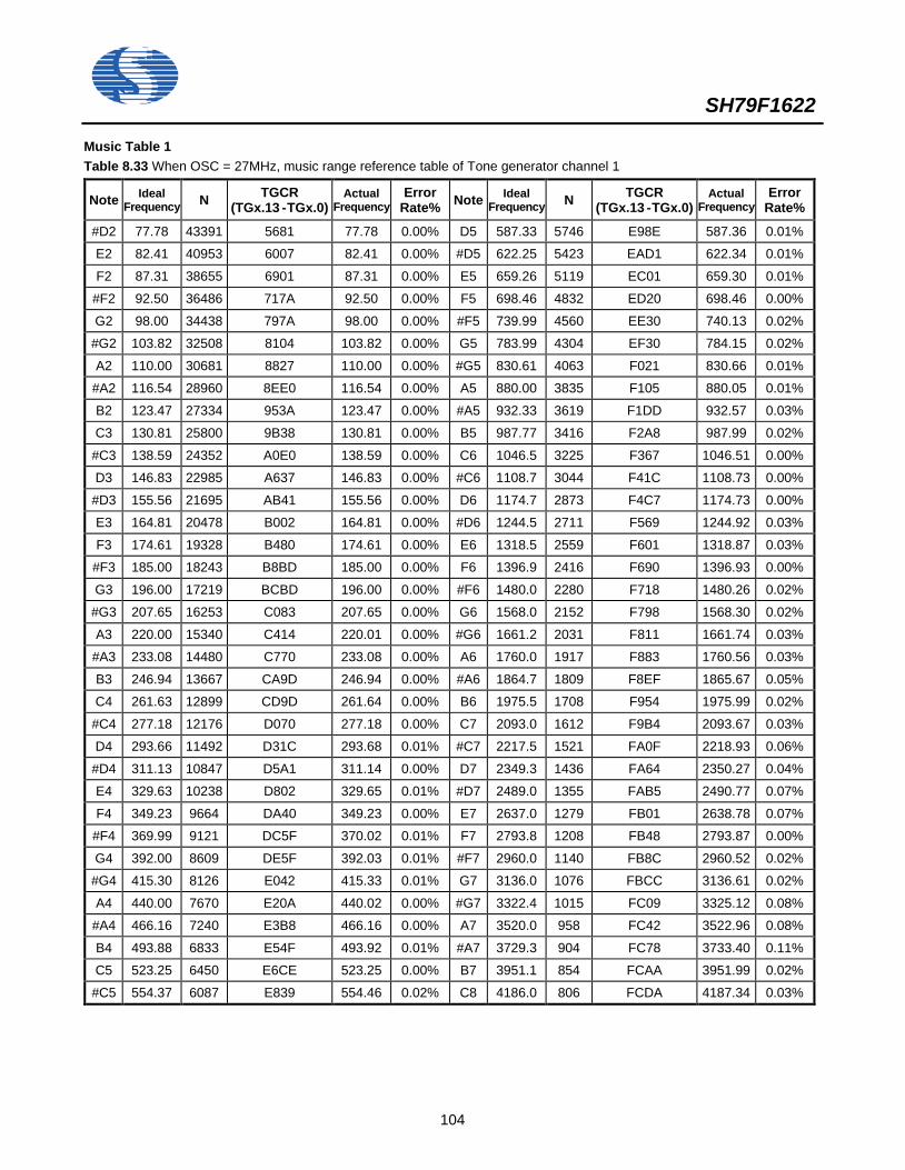
SH79F1622
104
Music Table 1 Table 8.33 When OSC = 27MHz, music range reference table of Tone generator channel 1
Note Ideal Frequency N TGCR
(TGx.13 - TGx.0) Actual
Frequency Error
Rate% Note Ideal Frequency N TGCR
(TGx.13 - TGx.0) Actual
Frequency Error
Rate%
#D2 77.78 43391 5681 77.78 0.00% D5 587.33 5746 E98E 587.36 0.01%
E2 82.41 40953 6007 82.41 0.00% #D5 622.25 5423 EAD1 622.34 0.01%
F2 87.31 38655 6901 87.31 0.00% E5 659.26 5119 EC01 659.30 0.01%
#F2 92.50 36486 717A 92.50 0.00% F5 698.46 4832 ED20 698.46 0.00%
G2 98.00 34438 797A 98.00 0.00% #F5 739.99 4560 EE30 740.13 0.02%
#G2 103.82 32508 8104 103.82 0.00% G5 783.99 4304 EF30 784.15 0.02%
A2 110.00 30681 8827 110.00 0.00% #G5 830.61 4063 F021 830.66 0.01%
#A2 116.54 28960 8EE0 116.54 0.00% A5 880.00 3835 F105 880.05 0.01%
B2 123.47 27334 953A 123.47 0.00% #A5 932.33 3619 F1DD 932.57 0.03%
C3 130.81 25800 9B38 130.81 0.00% B5 987.77 3416 F2A8 987.99 0.02%
#C3 138.59 24352 A0E0 138.59 0.00% C6 1046.5 3225 F367 1046.51 0.00%
D3 146.83 22985 A637 146.83 0.00% #C6 1108.7 3044 F41C 1108.73 0.00%
#D3 155.56 21695 AB41 155.56 0.00% D6 1174.7 2873 F4C7 1174.73 0.00%
E3 164.81 20478 B002 164.81 0.00% #D6 1244.5 2711 F569 1244.92 0.03%
F3 174.61 19328 B480 174.61 0.00% E6 1318.5 2559 F601 1318.87 0.03%
#F3 185.00 18243 B8BD 185.00 0.00% F6 1396.9 2416 F690 1396.93 0.00%
G3 196.00 17219 BCBD 196.00 0.00% #F6 1480.0 2280 F718 1480.26 0.02%
#G3 207.65 16253 C083 207.65 0.00% G6 1568.0 2152 F798 1568.30 0.02%
A3 220.00 15340 C414 220.01 0.00% #G6 1661.2 2031 F811 1661.74 0.03%
#A3 233.08 14480 C770 233.08 0.00% A6 1760.0 1917 F883 1760.56 0.03%
B3 246.94 13667 CA9D 246.94 0.00% #A6 1864.7 1809 F8EF 1865.67 0.05%
C4 261.63 12899 CD9D 261.64 0.00% B6 1975.5 1708 F954 1975.99 0.02%
#C4 277.18 12176 D070 277.18 0.00% C7 2093.0 1612 F9B4 2093.67 0.03%
D4 293.66 11492 D31C 293.68 0.01% #C7 2217.5 1521 FA0F 2218.93 0.06%
#D4 311.13 10847 D5A1 311.14 0.00% D7 2349.3 1436 FA64 2350.27 0.04%
E4 329.63 10238 D802 329.65 0.01% #D7 2489.0 1355 FAB5 2490.77 0.07%
F4 349.23 9664 DA40 349.23 0.00% E7 2637.0 1279 FB01 2638.78 0.07%
#F4 369.99 9121 DC5F 370.02 0.01% F7 2793.8 1208 FB48 2793.87 0.00%
G4 392.00 8609 DE5F 392.03 0.01% #F7 2960.0 1140 FB8C 2960.52 0.02%
#G4 415.30 8126 E042 415.33 0.01% G7 3136.0 1076 FBCC 3136.61 0.02%
A4 440.00 7670 E20A 440.02 0.00% #G7 3322.4 1015 FC09 3325.12 0.08%
#A4 466.16 7240 E3B8 466.16 0.00% A7 3520.0 958 FC42 3522.96 0.08%
B4 493.88 6833 E54F 493.92 0.01% #A7 3729.3 904 FC78 3733.40 0.11%
C5 523.25 6450 E6CE 523.25 0.00% B7 3951.1 854 FCAA 3951.99 0.02%
#C5 554.37 6087 E839 554.46 0.02% C8 4186.0 806 FCDA 4187.34 0.03%
SH79F1622
105
8.9 Power Management 8.9.1 Features
Two power saving modes: Idle mode and Power-Down mode Two ways to exit Idle and Power-Down mode: interrupt and reset
To reduce power consumption, SH79F1622 supplies two power saving modes: Idle mode and Power-Down mode. These two modes are controlled by PCON & SUSLO register. 8.9.2 Idle Mode In this mode, the clock to CPU is frozen, the program execution is halted, and the CPU will stop at a defined state. But the peripherals continue to be clocked. When entering idle mode, all the CPU status before entering will be preserved. Such as: PSW, PC, SFR & RAM are all retained. By two consecutive instructions: setting SUSLO register as 0x55, and immediately followed by setting the IDL bit in PCON register, will make SH79F1621 enter Idle mode. If the consecutive instruction sequence requirement is not met, the CPU will clear either SUSLO register or IDL bit in the next machine cycle. And the CPU will not enter Idle mode. The setting of IDL bit will be the last instruction that CPU executed. There are two ways to exit Idle mode: (1) An interrupt generated. The clock to the CPU will be restored, and the hardware will clear SUSLO register and IDL bit in
PCON register. Then the program will execute the interrupt service routine first, and then jumps to the instruction immediately following the instruction that activated Idle mode.
(2) Reset signal (logic low on the RESET pin, WDT RESET if enabled, LVR REST if enabled), this will restore the clock to the CPU, the SUSLO register and the IDL bit in PCON register will be cleared by hardware, finally the SH79F1622 will be reset. And the program will execute from address 0000H. The RAM will keep unchanged and the SFR value might be changed according to different function module.
8.9.3 Power-Down Mode The Power-Down mode places the SH79F1622 in a very low power state. Power-Down mode will stop all the clocks including CPU and peripherals. If WDT is enabled, WDT block will keep on working. When entering Power-Down mode, all the CPU status before entering will be preserved. Such as: PSW, PC, SFR & RAM are all retained. By two consecutive instructions: setting SUSLO register as 0x55, and immediately followed by setting the PD bit in PCON register, will make SH79F1622 enter Power-Down mode. If the consecutive instruction sequence requirement is not met, the CPU will clear either SUSLO register or PD bit in the next machine cycle. And the CPU will not enter Power-Down mode. The setting of PD bit will be the last instruction that CPU executed. Note: If IDL bit and PD bit are set simultaneously, the SH79F1621 enters Power-Down mode. The CPU will not go in Idle mode when exiting from Power-Down mode, and the hardware will clear both IDL & PD bit after exit form Power-Down mode. There are two ways to exit the Power-Down mode: (1) An active external Interrupt such as INT0, INT1, INT2, INT3 & INT4 will make SH79F1622 exit Power-Down mode. The
oscillator will start after interrupt happens, after warm-up time, the clocks to the CPU and peripheral will be restored, the SUSLO register and PD bit in PCON register will be cleared by hardware. Program execution resumes with the interrupt service routine. After completion of the interrupt service routine, program execution resumes with the instruction immediately following the instruction that activated Power-Down mode.
(2) Reset signal (logic low on the RESET pin, WDT RESET if enabled, LVR REST if enabled). This will restore the clock to the CPU after warm-up time, the SUSLO register and the PD bit in PCON register will be cleared by hardware, finally the SH79F1622 will be reset. And the program will execute from address 0000H. The RAM will keep unchanged and the SFR value might be changed according to different function module.
Note: In order to entering Idle/Power-Down, it is necessary to add 3 NOPs after setting IDL/PD bit in PCON.
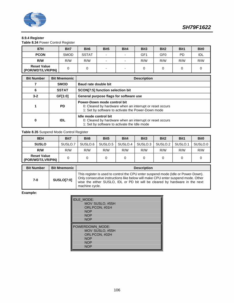
SH79F1622
106
8.9.4 Register Table 8.34 Power Control Register
87H Bit7 Bit6 Bit5 Bit4 Bit3 Bit2 Bit1 Bit0 PCON SMOD SSTAT - - GF1 GF0 PD IDL
R/W R/W R/W - - R/W R/W R/W R/W Reset Value
(POR/WDT/LVR/PIN) 0 0 - - 0 0 0 0
Bit Number Bit Mnemonic Description 7 SMOD Baud rate double bit
6 SSTAT SCON[7:5] function selection bit
3-2 GF[1:0] General purpose flags for software use
1 PD Power-Down mode control bit
0: Cleared by hardware when an interrupt or reset occurs 1: Set by software to activate the Power-Down mode
0 IDL Idle mode control bit
0: Cleared by hardware when an interrupt or reset occurs 1: Set by software to activate the Idle mode
Table 8.35 Suspend Mode Control Register
8EH Bit7 Bit6 Bit5 Bit4 Bit3 Bit2 Bit1 Bit0 SUSLO SUSLO.7 SUSLO.6 SUSLO.5 SUSLO.4 SUSLO.3 SUSLO.2 SUSLO.1 SUSLO.0
R/W R/W R/W R/W R/W R/W R/W R/W R/W Reset Value
(POR/WDT/LVR/PIN) 0 0 0 0 0 0 0 0
Bit Number Bit Mnemonic Description
7-0 SUSLO[7:0] This register is used to control the CPU enter suspend mode (Idle or Power-Down). Only consecutive instructions like below will make CPU enter suspend mode. Other wise the either SUSLO, IDL or PD bit will be cleared by hardware in the next machine cycle.
Example:
IDLE_MODE: MOV SUSLO, #55H ORL PCON, #01H NOP NOP NOP
POWERDOWN_MODE: MOV SUSLO, #55H ORL PCON, #02H NOP NOP NOP
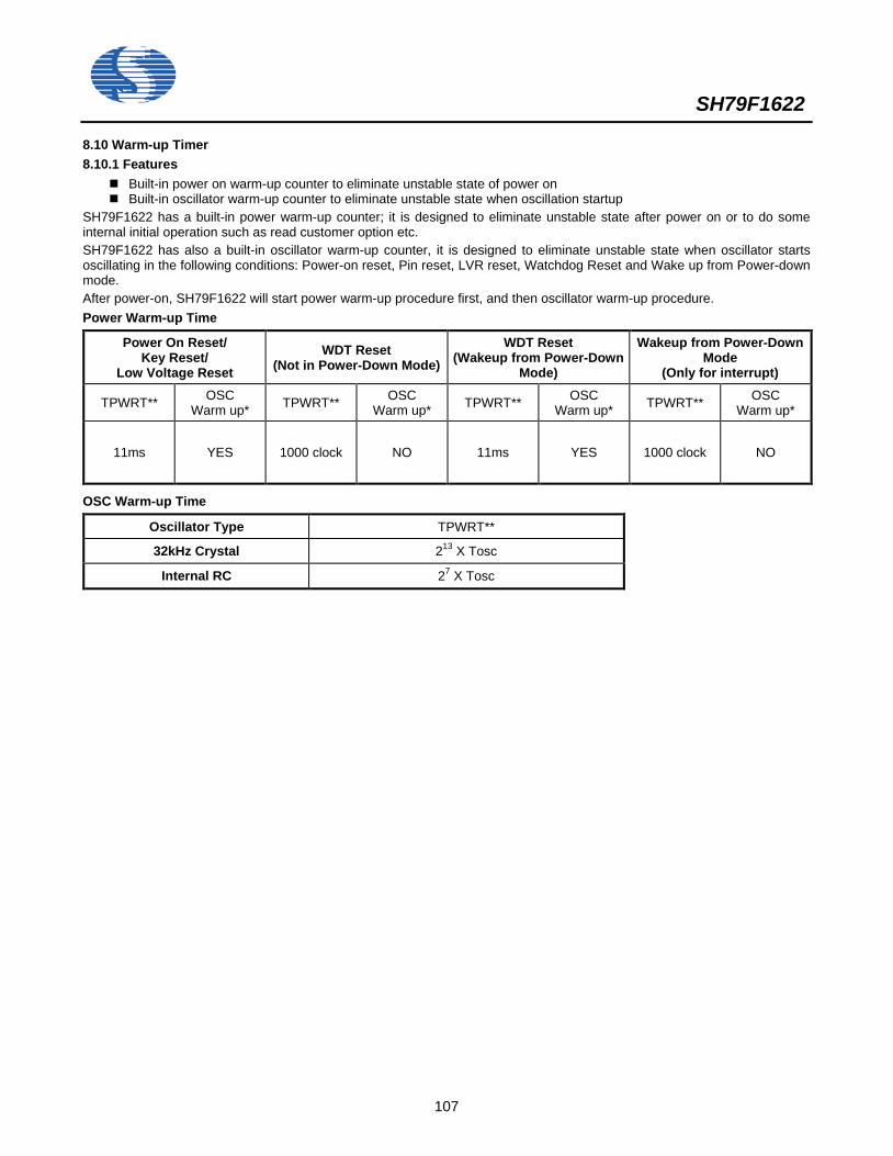
SH79F1622
107
8.10 Warm-up Timer 8.10.1 Features
Built-in power on warm-up counter to eliminate unstable state of power on Built-in oscillator warm-up counter to eliminate unstable state when oscillation startup
SH79F1622 has a built-in power warm-up counter; it is designed to eliminate unstable state after power on or to do some internal initial operation such as read customer option etc. SH79F1622 has also a built-in oscillator warm-up counter, it is designed to eliminate unstable state when oscillator starts oscillating in the following conditions: Power-on reset, Pin reset, LVR reset, Watchdog Reset and Wake up from Power-down mode. After power-on, SH79F1622 will start power warm-up procedure first, and then oscillator warm-up procedure. Power Warm-up Time
Power On Reset/ Key Reset/
Low Voltage Reset WDT Reset
(Not in Power-Down Mode) WDT Reset
(Wakeup from Power-Down Mode)
Wakeup from Power-Down Mode
(Only for interrupt)
TPWRT** OSC Warm up* TPWRT** OSC
Warm up* TPWRT** OSC Warm up* TPWRT** OSC
Warm up*
11ms YES 1000 clock NO 11ms YES 1000 clock NO
OSC Warm-up Time
Oscillator Type TPWRT**
32kHz Crystal 213 X Tosc
Internal RC 27 X Tosc
SH79F1622
108
8.11 Code Option OP_WDT:
0: Enable WDT (Default) 1: Disable WDT
OP_WDTPD: 0: WDT can’t work in STOP MODE (Default) 1: WDT can work in STOP MODE
OP_LVREN: 0: Disable LVR function (Default) 1: Enable LVR function
OP_LVRLE: 0: 4.1V LVR level 1 (Default) 1: 2.8V LVR level 2
OP_OSC: 000: Oscillator1 is internal 27M RC, oscillator2 is disabled 011: Oscillator1 is 32.768k crystal oscillator, oscillator2 is internal 27M RC
OP_LEDCOM: 0: P1.0 - P1.6 sink ability normal mode (Default) 1: P1.0 - P1.6 sink ability large mode
OP_RST: 0: P1.6 used as RST pin (Default) 1: P1.6 used as I/O pin
OP_SEG: 0: P0.0 - P0.7, P2.0 - P2.7 normal of output current capability (Default) 1: P0.0 - P0.7, P2.0 - P2.7 1/3 of normal of output current capability
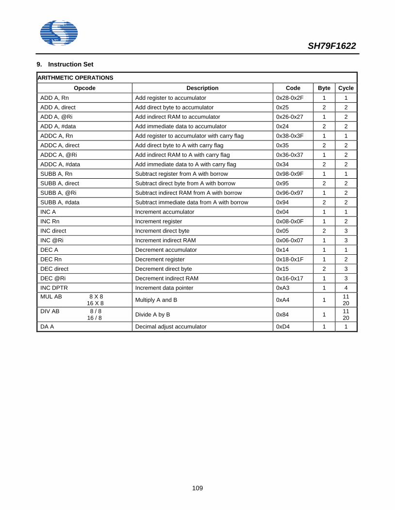
SH79F1622
109
9. Instruction Set
ARITHMETIC OPERATIONS
Opcode Description Code Byte Cycle ADD A, Rn Add register to accumulator 0x28-0x2F 1 1 ADD A, direct Add direct byte to accumulator 0x25 2 2 ADD A, @Ri Add indirect RAM to accumulator 0x26-0x27 1 2 ADD A, #data Add immediate data to accumulator 0x24 2 2 ADDC A, Rn Add register to accumulator with carry flag 0x38-0x3F 1 1 ADDC A, direct Add direct byte to A with carry flag 0x35 2 2 ADDC A, @Ri Add indirect RAM to A with carry flag 0x36-0x37 1 2 ADDC A, #data Add immediate data to A with carry flag 0x34 2 2 SUBB A, Rn Subtract register from A with borrow 0x98-0x9F 1 1 SUBB A, direct Subtract direct byte from A with borrow 0x95 2 2 SUBB A, @Ri Subtract indirect RAM from A with borrow 0x96-0x97 1 2 SUBB A, #data Subtract immediate data from A with borrow 0x94 2 2 INC A Increment accumulator 0x04 1 1 INC Rn Increment register 0x08-0x0F 1 2 INC direct Increment direct byte 0x05 2 3 INC @Ri Increment indirect RAM 0x06-0x07 1 3 DEC A Decrement accumulator 0x14 1 1 DEC Rn Decrement register 0x18-0x1F 1 2 DEC direct Decrement direct byte 0x15 2 3 DEC @Ri Decrement indirect RAM 0x16-0x17 1 3 INC DPTR Increment data pointer 0xA3 1 4 MUL AB 8 X 8
16 X 8 Multiply A and B 0xA4 1 11 20
DIV AB 8 / 8 16 / 8 Divide A by B 0x84 1 11
20 DA A Decimal adjust accumulator 0xD4 1 1
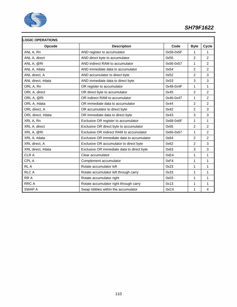
SH79F1622
110
LOGIC OPERATIONS
Opcode Description Code Byte Cycle ANL A, Rn AND register to accumulator 0x58-0x5F 1 1 ANL A, direct AND direct byte to accumulator 0x55 2 2 ANL A, @Ri AND indirect RAM to accumulator 0x56-0x57 1 2 ANL A, #data AND immediate data to accumulator 0x54 2 2 ANL direct, A AND accumulator to direct byte 0x52 2 3 ANL direct, #data AND immediate data to direct byte 0x53 3 3 ORL A, Rn OR register to accumulator 0x48-0x4F 1 1 ORL A, direct OR direct byte to accumulator 0x45 2 2 ORL A, @Ri OR indirect RAM to accumulator 0x46-0x47 1 2 ORL A, #data OR immediate data to accumulator 0x44 2 2 ORL direct, A OR accumulator to direct byte 0x42 2 3 ORL direct, #data OR immediate data to direct byte 0x43 3 3 XRL A, Rn Exclusive OR register to accumulator 0x68-0x6F 1 1 XRL A, direct Exclusive OR direct byte to accumulator 0x65 2 2 XRL A, @Ri Exclusive OR indirect RAM to accumulator 0x66-0x67 1 2 XRL A, #data Exclusive OR immediate data to accumulator 0x64 2 2 XRL direct, A Exclusive OR accumulator to direct byte 0x62 2 3 XRL direct, #data Exclusive OR immediate data to direct byte 0x63 3 3 CLR A Clear accumulator 0xE4 1 1 CPL A Complement accumulator 0xF4 1 1 RL A Rotate accumulator left 0x23 1 1 RLC A Rotate accumulator left through carry 0x33 1 1 RR A Rotate accumulator right 0x03 1 1 RRC A Rotate accumulator right through carry 0x13 1 1 SWAP A Swap nibbles within the accumulator 0xC4 1 4
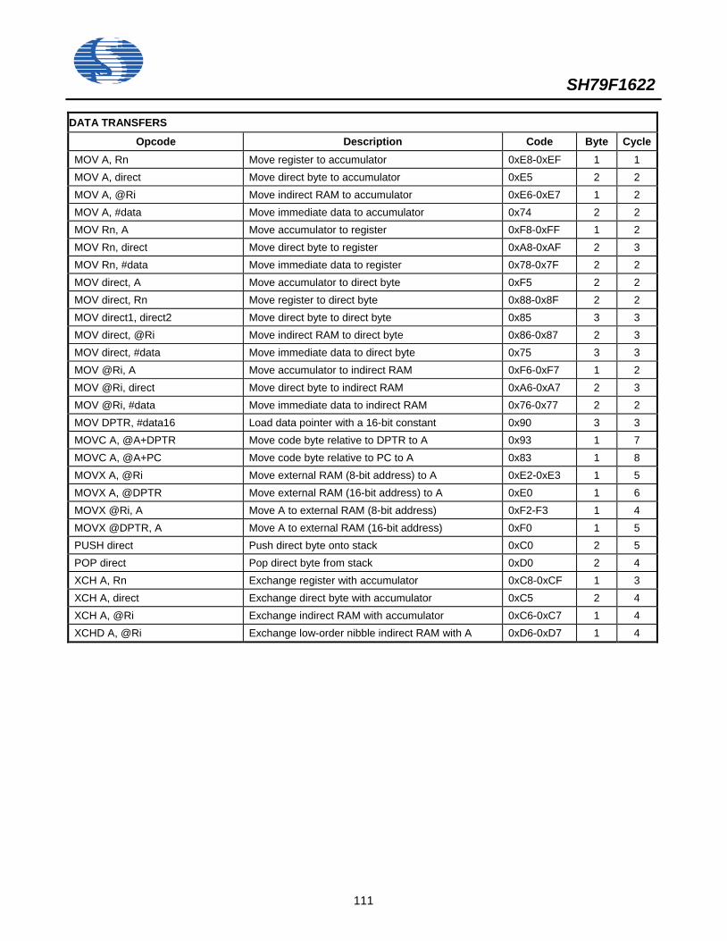
SH79F1622
111
DATA TRANSFERS
Opcode Description Code Byte Cycle MOV A, Rn Move register to accumulator 0xE8-0xEF 1 1 MOV A, direct Move direct byte to accumulator 0xE5 2 2 MOV A, @Ri Move indirect RAM to accumulator 0xE6-0xE7 1 2 MOV A, #data Move immediate data to accumulator 0x74 2 2 MOV Rn, A Move accumulator to register 0xF8-0xFF 1 2 MOV Rn, direct Move direct byte to register 0xA8-0xAF 2 3 MOV Rn, #data Move immediate data to register 0x78-0x7F 2 2 MOV direct, A Move accumulator to direct byte 0xF5 2 2 MOV direct, Rn Move register to direct byte 0x88-0x8F 2 2 MOV direct1, direct2 Move direct byte to direct byte 0x85 3 3 MOV direct, @Ri Move indirect RAM to direct byte 0x86-0x87 2 3 MOV direct, #data Move immediate data to direct byte 0x75 3 3 MOV @Ri, A Move accumulator to indirect RAM 0xF6-0xF7 1 2 MOV @Ri, direct Move direct byte to indirect RAM 0xA6-0xA7 2 3 MOV @Ri, #data Move immediate data to indirect RAM 0x76-0x77 2 2 MOV DPTR, #data16 Load data pointer with a 16-bit constant 0x90 3 3 MOVC A, @A+DPTR Move code byte relative to DPTR to A 0x93 1 7 MOVC A, @A+PC Move code byte relative to PC to A 0x83 1 8 MOVX A, @Ri Move external RAM (8-bit address) to A 0xE2-0xE3 1 5 MOVX A, @DPTR Move external RAM (16-bit address) to A 0xE0 1 6 MOVX @Ri, A Move A to external RAM (8-bit address) 0xF2-F3 1 4 MOVX @DPTR, A Move A to external RAM (16-bit address) 0xF0 1 5 PUSH direct Push direct byte onto stack 0xC0 2 5 POP direct Pop direct byte from stack 0xD0 2 4 XCH A, Rn Exchange register with accumulator 0xC8-0xCF 1 3 XCH A, direct Exchange direct byte with accumulator 0xC5 2 4 XCH A, @Ri Exchange indirect RAM with accumulator 0xC6-0xC7 1 4 XCHD A, @Ri Exchange low-order nibble indirect RAM with A 0xD6-0xD7 1 4
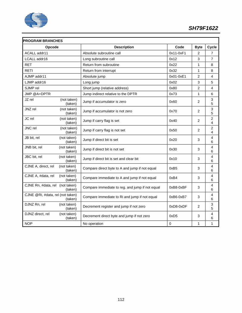
SH79F1622
112
PROGRAM BRANCHES
Opcode Description Code Byte Cycle ACALL addr11 Absolute subroutine call 0x11-0xF1 2 7 LCALL addr16 Long subroutine call 0x12 3 7 RET Return from subroutine 0x22 1 8 RETI Return from interrupt 0x32 1 8 AJMP addr11 Absolute jump 0x01-0xE1 2 4 LJMP addr16 Long jump 0x02 3 5 SJMP rel Short jump (relative address) 0x80 2 4 JMP @A+DPTR Jump indirect relative to the DPTR 0x73 1 6 JZ rel (not taken)
(taken) Jump if accumulator is zero 0x60 2 3 5
JNZ rel (not taken) (taken) Jump if accumulator is not zero 0x70 2 3
5 JC rel (not taken)
(taken) Jump if carry flag is set 0x40 2 2 4
JNC rel (not taken) (taken) Jump if carry flag is not set 0x50 2 2
4 JB bit, rel (not taken)
(taken) Jump if direct bit is set 0x20 3 4 6
JNB bit, rel (not taken) (taken) Jump if direct bit is not set 0x30 3 4
6 JBC bit, rel (not taken)
(taken) Jump if direct bit is set and clear bit 0x10 3 4 6
CJNE A, direct, rel (not taken) (taken) Compare direct byte to A and jump if not equal 0xB5 3 4
6 CJNE A, #data, rel (not taken)
(taken) Compare immediate to A and jump if not equal 0xB4 3 4 6
CJNE Rn, #data, rel (not taken) (taken) Compare immediate to reg. and jump if not equal 0xB8-0xBF 3 4
6 CJNE @Ri, #data, rel (not taken)
(taken) Compare immediate to Ri and jump if not equal 0xB6-0xB7 3 4 6
DJNZ Rn, rel (not taken) (taken) Decrement register and jump if not zero 0xD8-0xDF 2 3
5 DJNZ direct, rel (not taken)
(taken) Decrement direct byte and jump if not zero 0xD5 3 4 6
NOP No operation 0 1 1
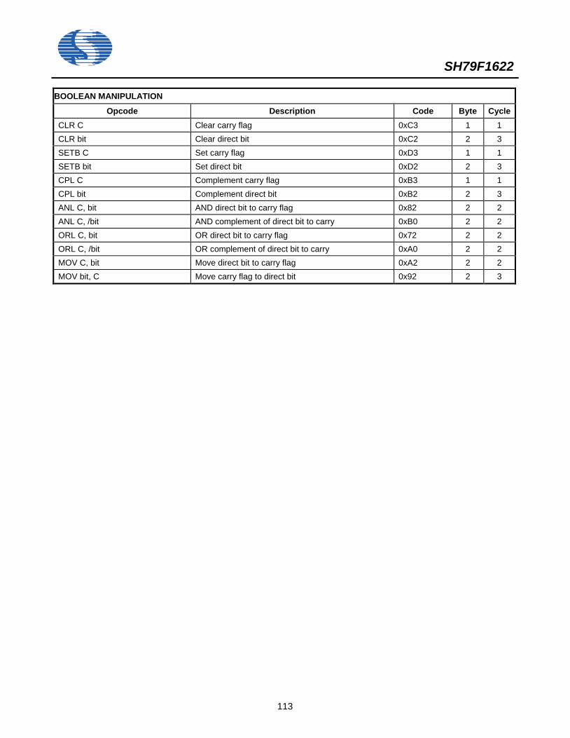
SH79F1622
113
BOOLEAN MANIPULATION
Opcode Description Code Byte Cycle CLR C Clear carry flag 0xC3 1 1 CLR bit Clear direct bit 0xC2 2 3 SETB C Set carry flag 0xD3 1 1 SETB bit Set direct bit 0xD2 2 3 CPL C Complement carry flag 0xB3 1 1 CPL bit Complement direct bit 0xB2 2 3 ANL C, bit AND direct bit to carry flag 0x82 2 2 ANL C, /bit AND complement of direct bit to carry 0xB0 2 2 ORL C, bit OR direct bit to carry flag 0x72 2 2 ORL C, /bit OR complement of direct bit to carry 0xA0 2 2 MOV C, bit Move direct bit to carry flag 0xA2 2 2 MOV bit, C Move carry flag to direct bit 0x92 2 3
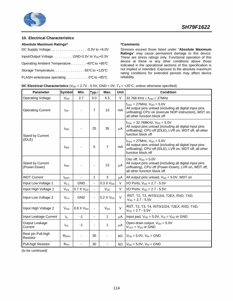
SH79F1622
114
10. Electrical Characteristics
Absolute Maximum Ratings* DC Supply Voltage. . . . . . . . . . . . . . . . . . . -0.3V to +6.0V
Input/Output Voltage. . . . . . . . . . .GND-0.3V to VDD+0.3V
Operating Ambient Temperature. . . . . . . . -40°C to +85°C
Storage Temperature. . . . . . . . . . . . . . . .-55°C to +125°C
FLASH write/erase operating. . . . . . . . . . . . 0°C to +85°C
*Comments Stresses exceed those listed under “Absolute Maximum Ratings” may cause permanent damage to this device. These are stress ratings only. Functional operation of this device at these or any other conditions above those indicated in the operational sections of this specification is not implied or intended. Exposure to the absolute maximum rating conditions for extended periods may affect device reliability.
DC Electrical Characteristics (VDD = 2.7V - 5.5V, GND = 0V, TA = +25°C, unless otherwise specified)
Parameter Symbol Min. Typ.∗ Max. Unit Condition Operating Voltage VDD 2.7 5.0 5.5 V 32.768 KHz ≤ fOSC ≤ 27MHz
Operating Current IOP - 7 13 mA
fOSC = 27MHz, VDD = 5.0V All output pins unload (including all digital input pins unfloating) CPU on (execute NOP instruction), WDT on, all other function block off
Stand by Current (IDLE)
ISB1 - 25 35 µA
fOSC = 32.768KHz, VDD = 5.0V All output pins unload (including all digital input pins unfloating), CPU off (IDLE), LVR on, WDT off, all other function block off
ISB2 - 5 7 mA
fOSC = 27MHz, VDD = 5.0V All output pins unload (including all digital input pins unfloating), CPU off (IDLE), LVR on, WDT off, all other function block off
Stand by Current (Power-Down) ISB3 - - 13 µA
Osc off, VDD = 5.0V All output pins unload (including all digital input pins unfloating), CPU off (Power-Down), LVR on, WDT off, all other function block off
WDT Current IWDT - 1 3 µA All output pins unload, VDD = 5.0V, WDT on
Input Low Voltage 1 VIL1 GND - 0.3 X VDD V I/O Ports, VDD = 2.7 - 5.5V
Input High Voltage 1 VIH1 0.7 X VDD - VDD V I/O Ports, VDD = 2.7 - 5.5V
Input Low Voltage 2 VIL2 GND - 0.2 X VDD V RST——-------——
, T2, T3, INT0/1/2/4, T2EX, RXD, TXD, VDD = 2.7 - 5.5V
Input High Voltage 2 VIH2 0.8 X VDD - VDD V RST——-------——
, T2, T3, T4, INT0/1/2/4, T2EX, RXD, TXD, VDD = 2.7 - 5.5V
Input Leakage Current IIL -1 - 1 µA Input pad, VDD = 5.0V, VIN = VDD or GND
Output Leakage Current IOL -1 - 1 µA Open-drain output, VDD = 5.0V
VOUT = VDD or GND
Rest pin Pull-high Resistor RRPH - 30 - kΩ VDD = 5.0V, VIN = GND
Pull-high Resistor RPH - 30 - kΩ VDD = 5.0V, VIN = GND
(to be continued)
SH79F1622
115
(continue)
Output High Voltage1 VOH1 VDD - 3V - - V I/O Ports, IOH = 40mA, VDD = 5.0V (OP_SEG = 0) P0.0-P0.7, P2.0-P2.7, output ability normal mode
Output High Voltage2 VOH2 VDD - 3V V I/O Ports, IOH = 14mA, VDD = 5.0V (OP_SEG = 1) P0.0-P0.7, P2.0-P2.7, output ability 1/3 normal mode
Output Low Voltage 1 VOL1 - - GND + 0.6 V I/O Port (P0, P1, P2, P3), IOL = 15mA, VDD = 5.0V (OP_LEDCOM = 0)
large drive port sink current capability IOL 88 100 - mA
COM Port (P1.0-P1.6), VDD = 5.0V, VOL = GND + 0.3V Code_Option (OP_LEDCOM = 1) P1.0-P1.6 both Select large mode (Code Option)
Note: (1) “∗” Data in “Typ.” Column is at 5.0V, 25°C, unless otherwise specified. (2) Maximum value of the supply current to VDD is 150mA. (3) Maximum value of the output current from GND is 300mA.
Touch Key Electrical Characteristics (VDD = 2.7V - 5.5V, GND = 0V, TA = +25°C, unless otherwise specified)
Parameter Symbol Min. Typ.∗ Max. Unit Condition Operating Voltage VDD 2.7 - 5.5 V
Output Voltage1 VDDR1 3.9 4 4.1 V VDD = 4.5 - 5.5V
Output Voltage 2 VDDR2 2.9 3.0 3.1 V IVDDR2 = 0 - 20mA, VDD = 3.5 - 5.5V
Output Voltage 3 VDDR3 2.4 2.5 2.6 V IVDDR3 = 0 - 20mA, VDD = 3.0 - 5.5V
Output Voltage 4 VDDR4 1.9 2 2.1 V IVDDR4 = 0 - 20mA, VDD = 2.7 - 5.5V
Output Reference Voltage 1 VREF1 0.9 1 1.1 V VDD = 2.7 - 5.5V
Output Reference Voltage 2 VREF2 1.4 1.5 1.6 V VDD = 2.7 - 5.5V
Output Reference Voltage 3 VREF3 1.9 2.0 2.1 V VDD = 2.7 - 5.5V
Output Reference Voltage 4 VREF4 2.4 2.5 2.6 V VDD = 3.0 - 5.5V
AC Electrical Characteristics (VDD = 2.7V - 5.5V, GND = 0V, TA = +25°C, fOSC = 27MHz, unless otherwise specified)
Parameter Symbol Min. Typ. Max. Unit Condition Oscillator start time TOSC - - 1 s fOSC = 32.768kHz
RESET pulse width tRESET 10 - - µs
WDT RC Frequency fWDT - 1 2 kHz
Frequency Stability (RC) ∆ F|/F1 - - ±1 % RC oscillator: |F - 27MHz|/27MHz (VDD = 2.7- 5.5V, TA = 25°C)
Frequency Stability (RC) ∆ F|/F2 - - ±2.5 % RC oscillator: |F - 27MHz|/27MHz (VDD = 2.7- 5.5V,TA = -40°C - +85°C)
SH79F1622
116
Low Voltage Reset Electrical Characteristics (VDD = 2.7V - 5.5V, GND = 0V, TA = +25°C, unless otherwise specified)
Parameter Symbol Min. Typ. Max. Unit Condition
LVR Voltage 1 VLVR1 4.0 4.1 4.2 V LVR enabled VDD = 2.8V - 5.5V
LVR Voltage 2 VLVR2 2.7 2.8 2.9 V LVR enabled VDD = 2.0V - 5.5V
LVR Voltage Detection Hysteresis Window VSMTLV - 50 - mv
Drop-Down Pulse Width for LVR TLVR - 60 - µs
Analog Comparator Electrical Characteristics (VDD = 2.7 - 5.5V, GND = 0V, TA = +25°C, unless otherwise specified)
Parameter Symbol Min. Typ. Max. Unit Condition Input Offset Voltage VIO - 10 15 mV TA = 25°C
Offset voltage of Input Voltage with temperature changes VI1 - 3 5 mV TA = -40°C~85°C
Input Common-Mode Voltage Range VICM 0 - VDD-1V V
Response time Tres1 - 3 4 µs VDD = 5V, C1P = 2.5V, C1N = 0V
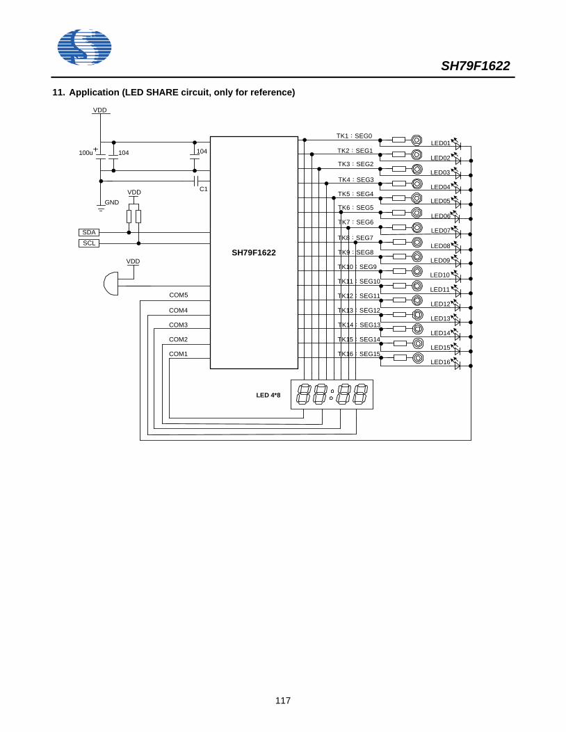
SH79F1622
117
11. Application (LED SHARE circuit, only for reference)
SH79F1622
GND
VDD
COM5
COM4
COM3
COM2
COM1
TK1:SEG0
TK2:SEG1
TK4:SEG3
TK3:SEG2
TK5:SEG4
TK6:SEG5
TK7:SEG6
TK8:SEG7
TK9:SEG8
TK10:SEG9
TK11:SEG10
TK12:SEG11
TK13:SEG12
TK14:SEG13
TK15:SEG14
TK16:SEG15
LED 4*8
LED02
LED03
LED04
LED05
LED06
LED07
LED08
LED09
LED10
LED11
LED12
LED13
LED14
LED15
LED16
LED01
C1
VDD
104104100u
SDA
SCL
VDD
SH79F1622
118
12. Ordering Information
Part No. Package
SH79F1622M/028MU SOP28
SH79F1622M/020MU SOP20
SH79F1622L/016LU SOP16
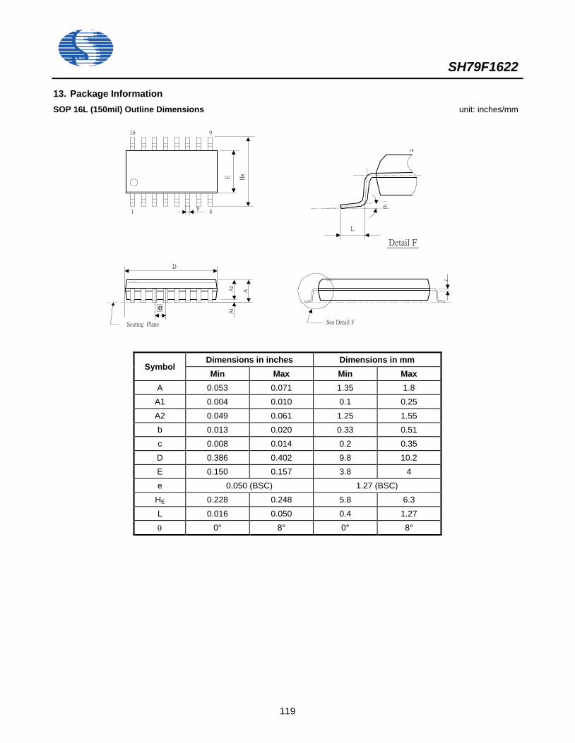
SH79F1622
119
13. Package Information SOP 16L (150mil) Outline Dimensions unit: inches/mm
1
L
c
8
See Detail F
916
Seating Plane
~ ~~
b
E HE
D
A1
A2
A
θ
e
Detail F
Symbol Dimensions in inches Dimensions in mm Min Max Min Max
A 0.053 0.071 1.35 1.8 A1 0.004 0.010 0.1 0.25 A2 0.049 0.061 1.25 1.55 b 0.013 0.020 0.33 0.51 c 0.008 0.014 0.2 0.35 D 0.386 0.402 9.8 10.2 E 0.150 0.157 3.8 4 e 0.050 (BSC) 1.27 (BSC)
HE 0.228 0.248 5.8 6.3 L 0.016 0.050 0.4 1.27
θ 0° 8° 0° 8°
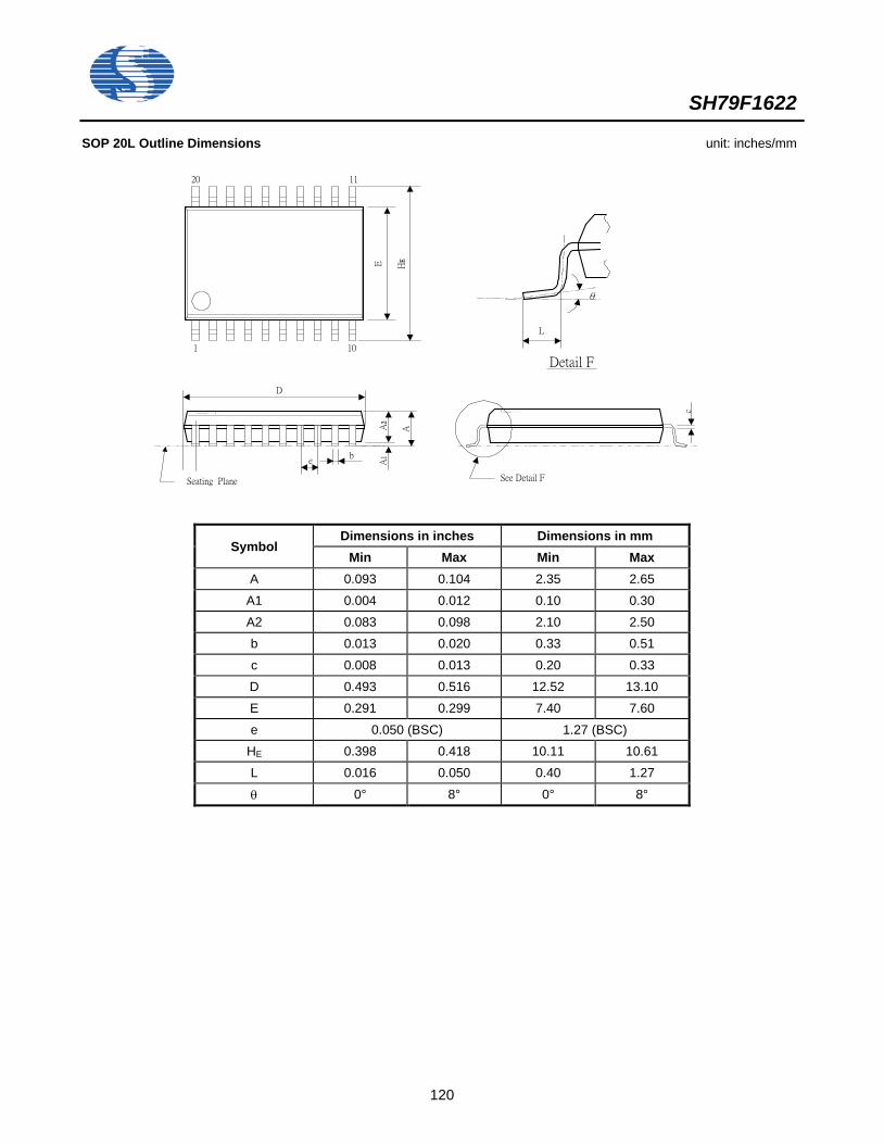
SH79F1622
120
SOP 20L Outline Dimensions unit: inches/mm
1
L
c
10
See Detail F
Detail F
1120
Seating Plane
b
E HE
DA
1A
2
A
θ
e
Symbol Dimensions in inches Dimensions in mm
Min Max Min Max A 0.093 0.104 2.35 2.65
A1 0.004 0.012 0.10 0.30 A2 0.083 0.098 2.10 2.50 b 0.013 0.020 0.33 0.51 c 0.008 0.013 0.20 0.33 D 0.493 0.516 12.52 13.10 E 0.291 0.299 7.40 7.60 e 0.050 (BSC) 1.27 (BSC)
HE 0.398 0.418 10.11 10.61 L 0.016 0.050 0.40 1.27
θ 0° 8° 0° 8°
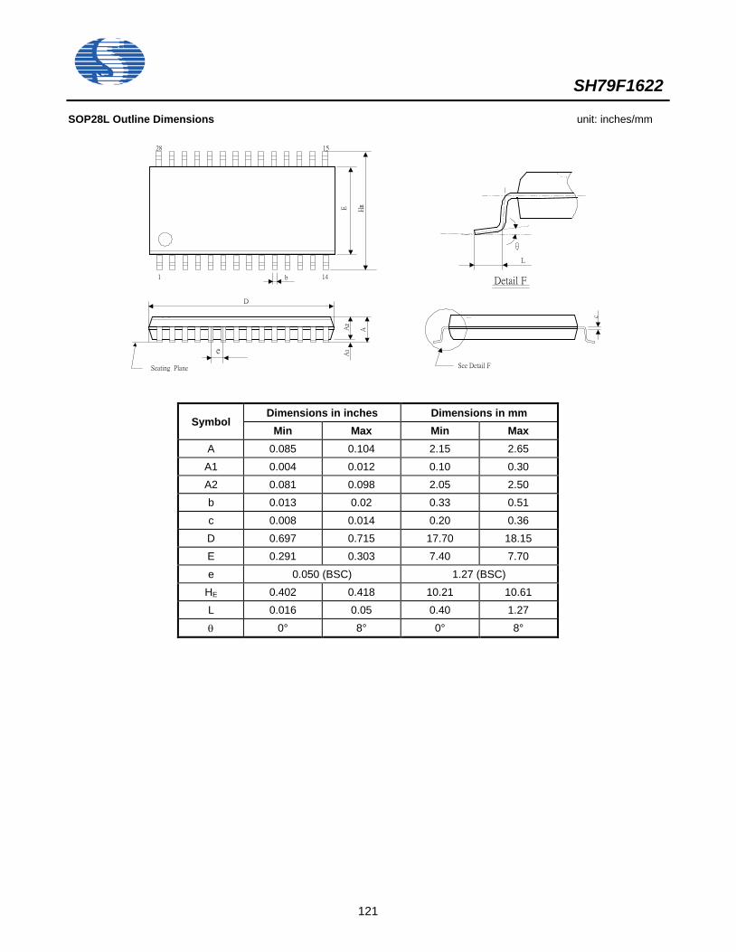
SH79F1622
121
SOP28L Outline Dimensions unit: inches/mm
1
E HE
L
c
14
See Detail F
Detail Fb
1528
A1
A2
A
D
Seating Plane
e
Symbol Dimensions in inches Dimensions in mm
Min Max Min Max A 0.085 0.104 2.15 2.65 A1 0.004 0.012 0.10 0.30 A2 0.081 0.098 2.05 2.50 b 0.013 0.02 0.33 0.51 c 0.008 0.014 0.20 0.36 D 0.697 0.715 17.70 18.15 E 0.291 0.303 7.40 7.70 e 0.050 (BSC) 1.27 (BSC)
HE 0.402 0.418 10.21 10.61 L 0.016 0.05 0.40 1.27
θ 0° 8° 0° 8°

SH79F1622
122
14. Product SPEC. Change Notice
Version Content Date
2.2 Original Sep. 2015
SH79F1622
123
Content 1. FEATURES ..................................................................................................................................................................... 1 2. GENERAL DESCRIPTION .............................................................................................................................................. 1 3. BLOCK DIAGRAM .......................................................................................................................................................... 2 4. PIN CONFIGURATION ................................................................................................................................................... 3 5. PIN DESCRIPTION ......................................................................................................................................................... 6 6. SFR MAPPING ................................................................................................................................................................ 7 7. NORMAL FUNCTION ................................................................................................................................................... 17 7.1 CPU .................................................................................................................................................................................................... 17
7.1.1 CPU Core SFR ............................................................................................................................................................................ 17 7.1.2 Enhanced CPU core SFRs ........................................................................................................................................................... 18 7.1.3 Register ........................................................................................................................................................................................ 18
7.2 RAM ................................................................................................................................................................................................... 19 7.2.1 Features ....................................................................................................................................................................................... 19
7.3 FLASH PROGRAM MEMORY .................................................................................................................................................................. 20 7.3.1 Features ....................................................................................................................................................................................... 20 7.3.2 Flash Operation in ICP Mode ..................................................................................................................................................... 22
7.4 SSP FUNCTION ..................................................................................................................................................................................... 23 7.4.1 SSP Register ................................................................................................................................................................................ 23 7.4.2 Flash Control Flow...................................................................................................................................................................... 26 7.4.3 SSP Programming Notice ............................................................................................................................................................ 27 7.4.4 Readable Random Code............................................................................................................................................................... 27
7.5 SYSTEM CLOCK AND OSCILLATOR ....................................................................................................................................................... 28 7.5.1 Features ...................................................................................................................................................................................... 28 7.5.2 Clock Definition ........................................................................................................................................................................... 28 7.5.3 Description .................................................................................................................................................................................. 29 7.5.4 Register ........................................................................................................................................................................................ 29 7.5.5 Oscillator Type ............................................................................................................................................................................ 30 7.5.6 Capacitor Selection for Oscillator ............................................................................................................................................... 30
7.6 I/O PORT .............................................................................................................................................................................................. 31 7.6.1 Features ....................................................................................................................................................................................... 31 7.6.2 Register ........................................................................................................................................................................................ 31 7.6.3 Port Diagram ............................................................................................................................................................................... 33 7.6.4 Port Share .................................................................................................................................................................................... 33
7.7 TIMER .................................................................................................................................................................................................. 36 7.7.1 Features ....................................................................................................................................................................................... 36 7.7.2 Timer2 ......................................................................................................................................................................................... 36 7.7.3 Timer3 ......................................................................................................................................................................................... 41 7.7.4 Timer4 ......................................................................................................................................................................................... 43
7.8 INTERRUPT ........................................................................................................................................................................................... 46 7.8.1 Features ....................................................................................................................................................................................... 46 7.8.2 Interrupt Enable Control ............................................................................................................................................................. 46 7.8.3 Registers ...................................................................................................................................................................................... 46 7.8.4 Interrupt Flag .............................................................................................................................................................................. 48 7.8.5 Interrupt Vector ........................................................................................................................................................................... 50 7.8.6 Interrupt Priority ......................................................................................................................................................................... 50 7.8.7 Interrupt Handling ....................................................................................................................................................................... 51 7.8.8 Interrupt Response Time .............................................................................................................................................................. 51 7.8.9 External Interrupt Inputs ............................................................................................................................................................. 52 7.8.10 Interrupt Summary ..................................................................................................................................................................... 53
8. ENHANCED FUNCTION ............................................................................................................................................... 54 8.1 TOUCH KEY FUNCTION ........................................................................................................................................................................ 54
8.1.1 Register ........................................................................................................................................................................................ 57 8.2 LED DRIVER ....................................................................................................................................................................................... 66
8.2.1 Register ........................................................................................................................................................................................ 66 8.2.2 Configuration of LED RAM ......................................................................................................................................................... 69
8.3 TOUCH KEY FUNCTION AND LED SHARE FUNCTION .......................................................................................................................... 71 8.3.1 Function Description ................................................................................................................................................................... 72 8.3.2 SHARE Table of SEG Port ........................................................................................................................................................... 72
8.4 EUART ............................................................................................................................................................................................... 73 8.4.1 Features ....................................................................................................................................................................................... 73 8.4.2 EUART Mode Description ........................................................................................................................................................... 73
SH79F1622
124
8.4.3 Baud Rate Generate ..................................................................................................................................................................... 78 8.4.4 Multi-Processor Communication ................................................................................................................................................. 78 8.4.5 Error Detection ............................................................................................................................................................................ 79 8.4.6 Register ........................................................................................................................................................................................ 80
8.5 TWI ..................................................................................................................................................................................................... 83 8.5.1 Features ....................................................................................................................................................................................... 83 8.5.2 Data Transformat ........................................................................................................................................................................ 83 8.5.3 Function Description ................................................................................................................................................................... 85 8.5.4 Transmission Mode ...................................................................................................................................................................... 87 8.5.5 Register ........................................................................................................................................................................................ 96
8.6 LOW VOLTAGE RESET (LVR) ............................................................................................................................................................... 99 8.6.1 Features ....................................................................................................................................................................................... 99
8.7 WATCHDOG TIMER (WDT) AND RESET STATE ................................................................................................................................... 100 8.7.1 Features ..................................................................................................................................................................................... 100 8.7.2 Register ...................................................................................................................................................................................... 101
8.8 TONE ................................................................................................................................................................................................. 102 8.9 POWER MANAGEMENT ....................................................................................................................................................................... 105
8.9.1 Features ..................................................................................................................................................................................... 105 8.9.2 Idle Mode ................................................................................................................................................................................... 105 8.9.3 Power-Down Mode .................................................................................................................................................................... 105 8.9.4 Register ...................................................................................................................................................................................... 106
8.10 WARM-UP TIMER ............................................................................................................................................................................. 107 8.10.1 Features ................................................................................................................................................................................... 107
8.11 CODE OPTION .................................................................................................................................................................................. 108 9. INSTRUCTION SET .................................................................................................................................................... 109 10. ELECTRICAL CHARACTERISTICS ........................................................................................................................ 114 11. APPLICATION (LED SHARE CIRCUIT, ONLY FOR REFERENCE) ....................................................................... 117 12. ORDERING INFORMATION ................................................................................................................................... 118 13. PACKAGE INFORMATION ..................................................................................................................................... 119 14. PRODUCT SPEC. CHANGE NOTICE..................................................................................................................... 122