Embed Size (px)
Citation preview
© September 20, 2006 Dr. Lynn Fuller
RIT’s Advanced CMOS Process
Page 1
Rochester Institute of TechnologyMicroelectronic Engineering
9-20-06 AdvCmos2006.ppt
EE-612 Lecture 23: CMOS Process Flow
EE-612:Lecture 18B:
CMOS Process Flow
Mark LundstromElectrical and Computer Engineering
Purdue UniversityWest Lafayette, IN USA
Fall 2008
www.nanohub.orgNCN
© September 20, 2006 Dr. Lynn Fuller
RIT’s Advanced CMOS Process
Page 2
Rochester Institute of TechnologyMicroelectronic Engineering
Acknowledgement to Dr. Lynn Fuller, RIT
9-20-06 AdvCmos2006.ppt
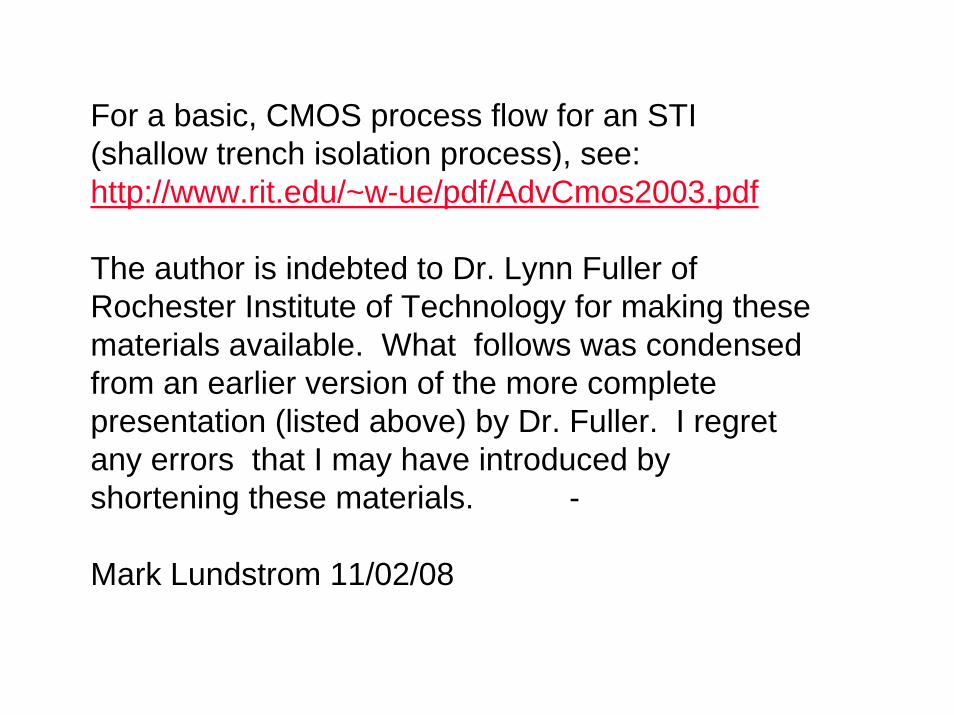
For a basic, CMOS process flow for an STI (shallow trench isolation process), see: http://www.rit.edu/~w-ue/pdf/AdvCmos2003.pdf
The author is indebted to Dr. Lynn Fuller of Rochester Institute of Technology for making these materials available. What follows was condensed from an earlier version of the more complete presentation (listed above) by Dr. Fuller. I regret any errors that I may have introduced by shortening these materials. -
Mark Lundstrom 11/02/08
© September 20, 2006 Dr. Lynn Fuller
RIT’s Advanced CMOS Process
Page 3
Rochester Institute of TechnologyMicroelectronic Engineering
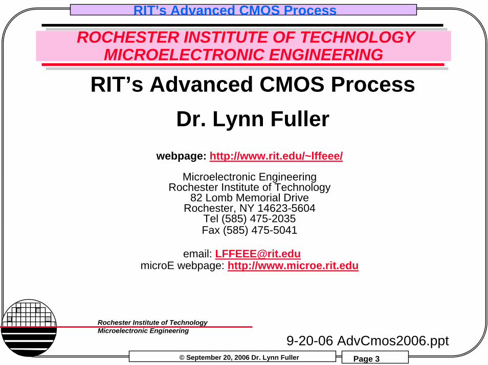
ROCHESTER INSTITUTE OF TECHNOLOGYMICROELECTRONIC ENGINEERING
RIT’s Advanced CMOS Process Dr. Lynn Fuller
webpage: http://www.rit.edu/~lffeee/
Microelectronic Engineering Rochester Institute of Technology 82 Lomb Memorial Drive Rochester, NY 14623-5604 Tel (585) 475-2035 Fax (585) 475-5041
email: [email protected] microE webpage: http://www.microe.rit.edu
9-20-06 AdvCmos2006.ppt
© September 20, 2006 Dr. Lynn Fuller
RIT’s Advanced CMOS Process
Page 4
Rochester Institute of TechnologyMicroelectronic Engineering
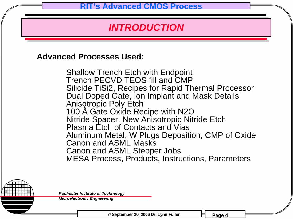
INTRODUCTION
Advanced Processes Used:
Shallow Trench Etch with EndpointTrench PECVD TEOS fill and CMPSilicide TiSi2, Recipes for Rapid Thermal ProcessorDual Doped Gate, Ion Implant and Mask DetailsAnisotropic Poly Etch100 Å Gate Oxide Recipe with N2ONitride Spacer, New Anisotropic Nitride EtchPlasma Etch of Contacts and ViasAluminum Metal, W Plugs Deposition, CMP of OxideCanon and ASML MasksCanon and ASML Stepper JobsMESA Process, Products, Instructions, Parameters
© September 20, 2006 Dr. Lynn Fuller
RIT’s Advanced CMOS Process
Page 5
Rochester Institute of TechnologyMicroelectronic Engineering
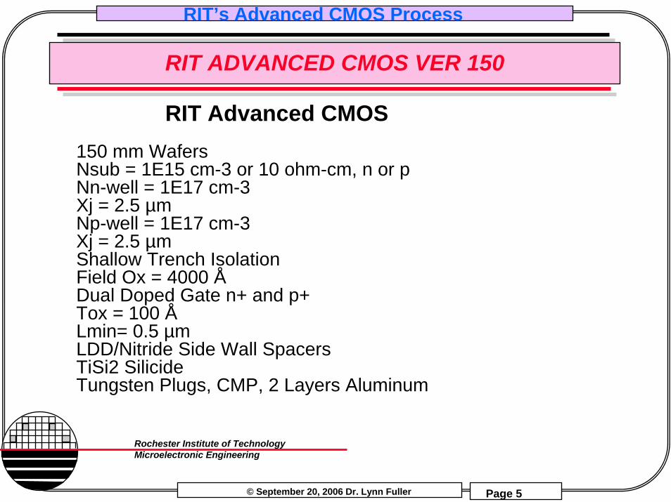
RIT ADVANCED CMOS VER 150
RIT Advanced CMOS150 mm WafersNsub = 1E15 cm-3 or 10 ohm-cm, n or pNn-well = 1E17 cm-3Xj = 2.5 µmNp-well = 1E17 cm-3Xj = 2.5 µmShallow Trench IsolationField Ox = 4000 ÅDual Doped Gate n+ and p+Tox = 100 ÅLmin= 0.5 µmLDD/Nitride Side Wall SpacersTiSi2 SilicideTungsten Plugs, CMP, 2 Layers Aluminum
© September 20, 2006 Dr. Lynn Fuller
RIT’s Advanced CMOS Process
Page 6
Rochester Institute of TechnologyMicroelectronic Engineering
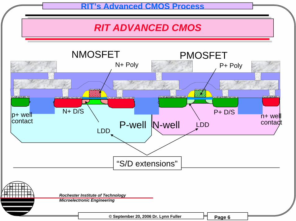
RIT ADVANCED CMOS
NMOSFET PMOSFET
N-wellP-well
N+ Poly
P+ D/SN+ D/S
LDDLDD
n+ wellcontact
p+ wellcontact
P+ Poly
“S/D extensions”
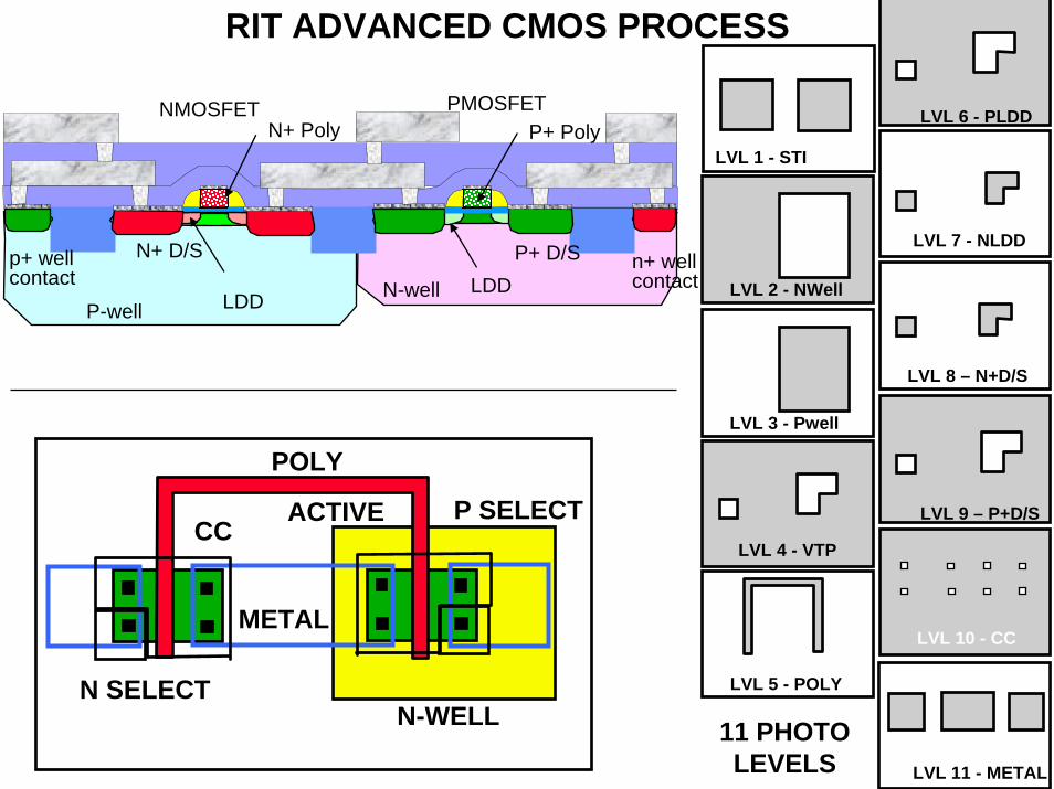
RIT ADVANCED CMOS PROCESS
11 PHOTOLEVELS
POLY
METAL
N-WELL
P SELECTCC
ACTIVE
N SELECT
LVL 2 - NWell
LVL 3 - Pwell
LVL 5 - POLY
LVL 7 - NLDD
LVL 10 - CC
LVL 11 - METAL
LVL 8 – N+D/S
LVL 9 – P+D/S
LVL 1 - STI
LVL 6 - PLDD
LVL 4 - VTP
NMOSFET PMOSFET
N-wellP-well
N+ Poly
P+ D/SN+ D/S
LDDLDD
n+ wellcontact
p+ wellcontact
P+ Poly
© September 20, 2006 Dr. Lynn Fuller
RIT’s Advanced CMOS Process
Page 8
Rochester Institute of TechnologyMicroelectronic Engineering
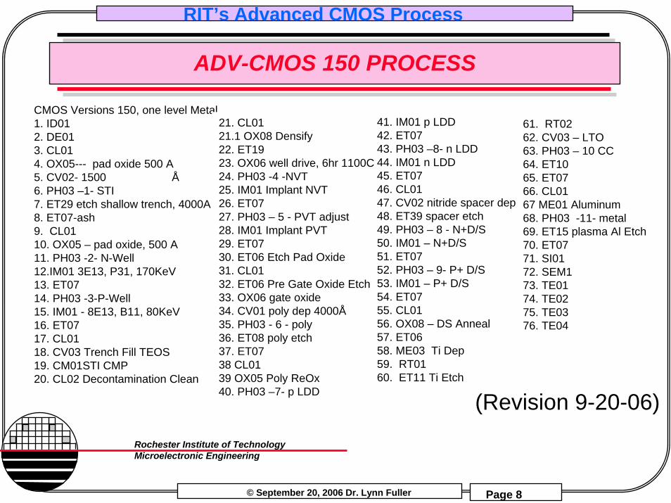
ADV-CMOS 150 PROCESS
CMOS Versions 150, one level Metal1. ID012. DE013. CL014. OX05--- pad oxide 500 A5. CV02- 1500 Å6. PH03 –1- STI7. ET29 etch shallow trench, 4000A8. ET07-ash9. CL0110. OX05 – pad oxide, 500 A11. PH03 -2- N-Well12.IM01 3E13, P31, 170KeV13. ET0714. PH03 -3-P-Well15. IM01 - 8E13, B11, 80KeV16. ET0717. CL0118. CV03 Trench Fill TEOS19. CM01STI CMP20. CL02 Decontamination Clean
21. CL0121.1 OX08 Densify22. ET1923. OX06 well drive, 6hr 1100C24. PH03 -4 -NVT25. IM01 Implant NVT26. ET0727. PH03 – 5 - PVT adjust28. IM01 Implant PVT29. ET0730. ET06 Etch Pad Oxide31. CL0132. ET06 Pre Gate Oxide Etch33. OX06 gate oxide34. CV01 poly dep 4000Å35. PH03 - 6 - poly36. ET08 poly etch37. ET0738 CL0139 OX05 Poly ReOx40. PH03 –7- p LDD
41. IM01 p LDD42. ET07 43. PH03 –8- n LDD44. IM01 n LDD45. ET0746. CL0147. CV02 nitride spacer dep48. ET39 spacer etch49. PH03 – 8 - N+D/S50. IM01 – N+D/S51. ET0752. PH03 – 9- P+ D/S53. IM01 – P+ D/S54. ET0755. CL0156. OX08 – DS Anneal57. ET0658. ME03 Ti Dep59. RT0160. ET11 Ti Etch
61. RT0262. CV03 – LTO63. PH03 – 10 CC64. ET1065. ET0766. CL0167 ME01 Aluminum68. PH03 -11- metal69. ET15 plasma Al Etch70. ET0771. SI0172. SEM173. TE0174. TE0275. TE0376. TE04
(Revision 9-20-06)
© September 20, 2006 Dr. Lynn Fuller
RIT’s Advanced CMOS Process
Page 9
Rochester Institute of TechnologyMicroelectronic Engineering
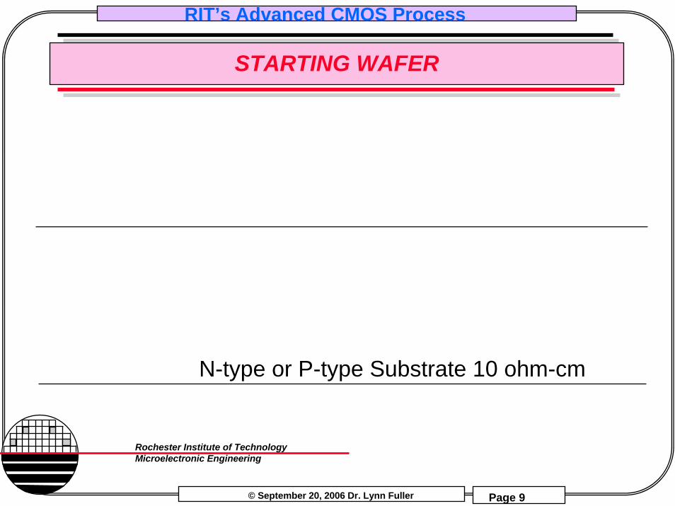
STARTING WAFER
N-type or P-type Substrate 10 ohm-cm
© September 20, 2006 Dr. Lynn Fuller
RIT’s Advanced CMOS Process
Page 10
Rochester Institute of TechnologyMicroelectronic Engineering
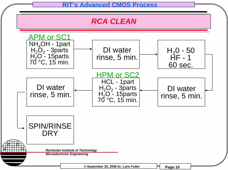
RCA CLEAN
DI waterrinse, 5 min.
H20 - 50HF - 160 sec.
HPM or SC2HCL - 1part
H2O2 - 3partsH2O - 15parts70 °C, 15 min.
SPIN/RINSEDRY
APM or SC1NH4OH - 1partH2O2 - 3partsH2O - 15parts70 °C, 15 min.
DI waterrinse, 5 min.
DI waterrinse, 5 min.
© September 20, 2006 Dr. Lynn Fuller
RIT’s Advanced CMOS Process
Page 11
Rochester Institute of TechnologyMicroelectronic Engineering
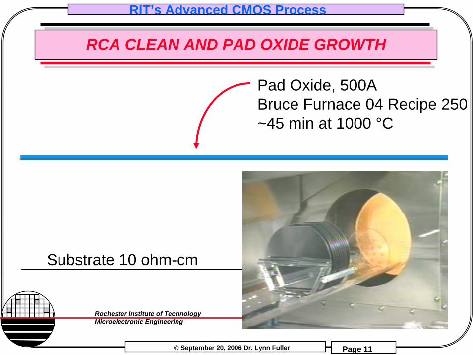
RCA CLEAN AND PAD OXIDE GROWTH
Pad Oxide, 500ABruce Furnace 04 Recipe 250~45 min at 1000 °C
Substrate 10 ohm-cm
© September 20, 2006 Dr. Lynn Fuller
RIT’s Advanced CMOS Process
Page 12
Rochester Institute of TechnologyMicroelectronic Engineering
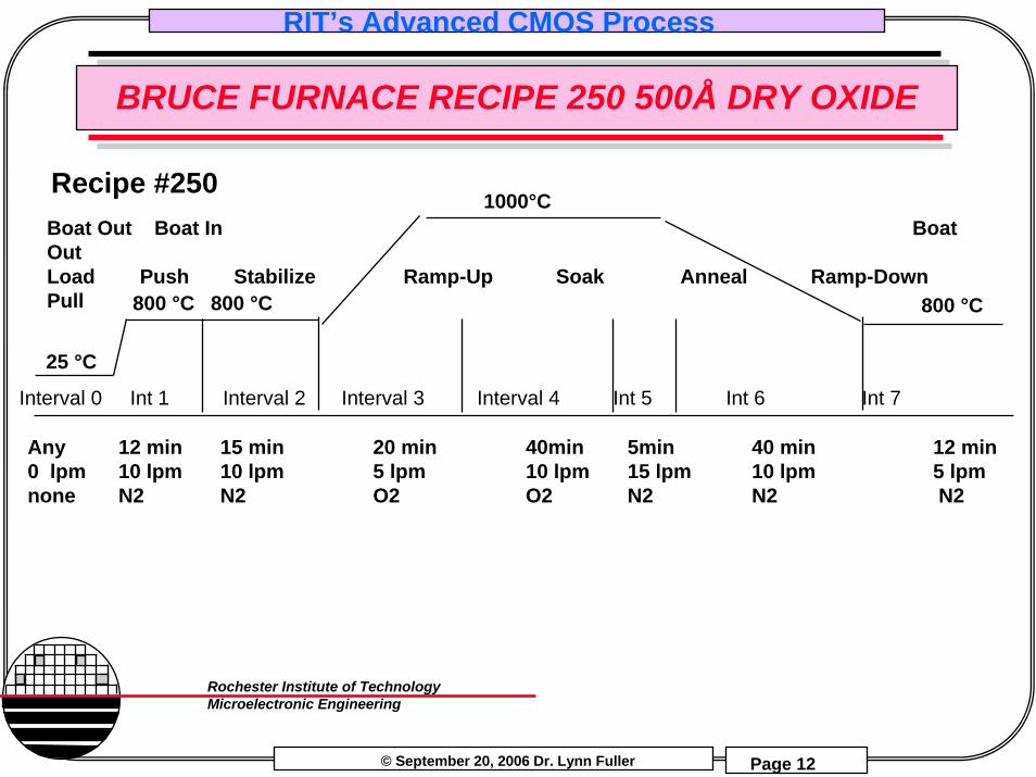
BRUCE FURNACE RECIPE 250 500Å DRY OXIDE
1000°C
800 °C
Boat Out Boat In Boat OutLoad Push Stabilize Ramp-Up Soak Anneal Ramp-DownPull
12 min 15 min 20 min 40min 5min 40 min 12 min10 lpm 10 lpm 5 lpm 10 lpm 15 lpm 10 lpm 5 lpmN2 N2 O2 O2 N2 N2 N2
Recipe #250
Interval 0 Int 1 Interval 2 Interval 3 Interval 4 Int 5 Int 6 Int 7
800 °C
25 °C
800 °C
Any0 lpmnone
© September 20, 2006 Dr. Lynn Fuller
RIT’s Advanced CMOS Process
Page 13
Rochester Institute of TechnologyMicroelectronic Engineering
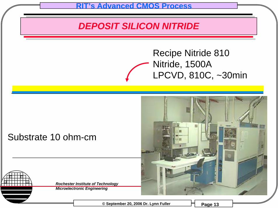
DEPOSIT SILICON NITRIDE
Substrate 10 ohm-cm
Recipe Nitride 810Nitride, 1500ALPCVD, 810C, ~30min
© September 20, 2006 Dr. Lynn Fuller
RIT’s Advanced CMOS Process
Page 14
Rochester Institute of TechnologyMicroelectronic Engineering
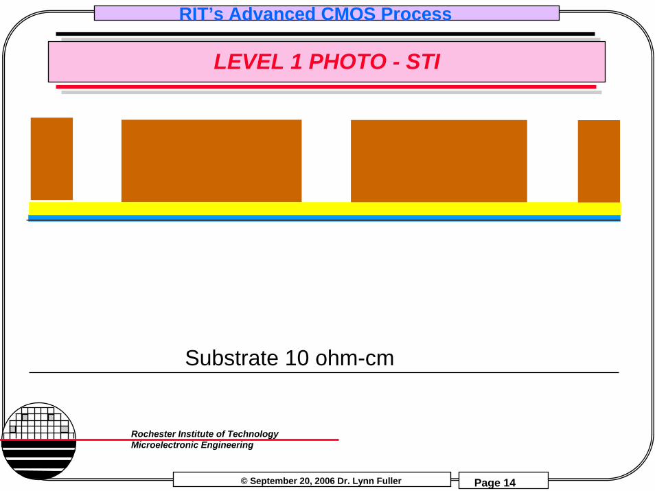
LEVEL 1 PHOTO - STI
Substrate 10 ohm-cm
© September 20, 2006 Dr. Lynn Fuller
RIT’s Advanced CMOS Process
Page 15
Rochester Institute of TechnologyMicroelectronic Engineering
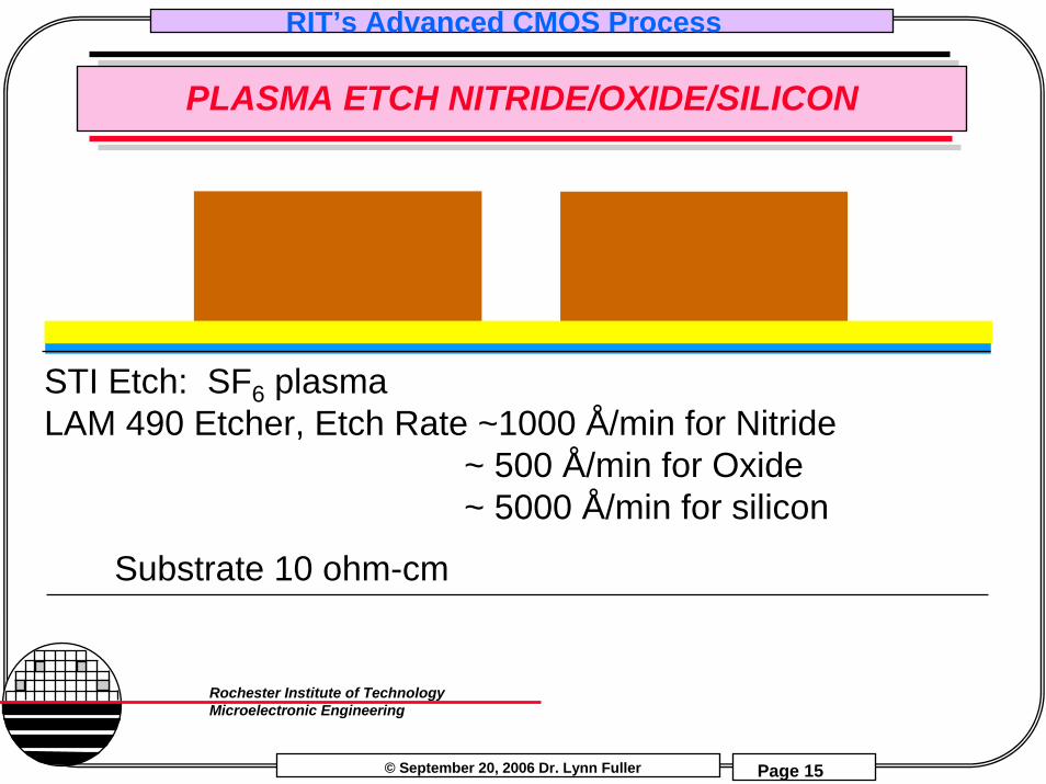
PLASMA ETCH NITRIDE/OXIDE/SILICON
STI Etch: SF6 plasmaLAM 490 Etcher, Etch Rate ~1000 Å/min for Nitride
~ 500 Å/min for Oxide~ 5000 Å/min for silicon
Substrate 10 ohm-cm
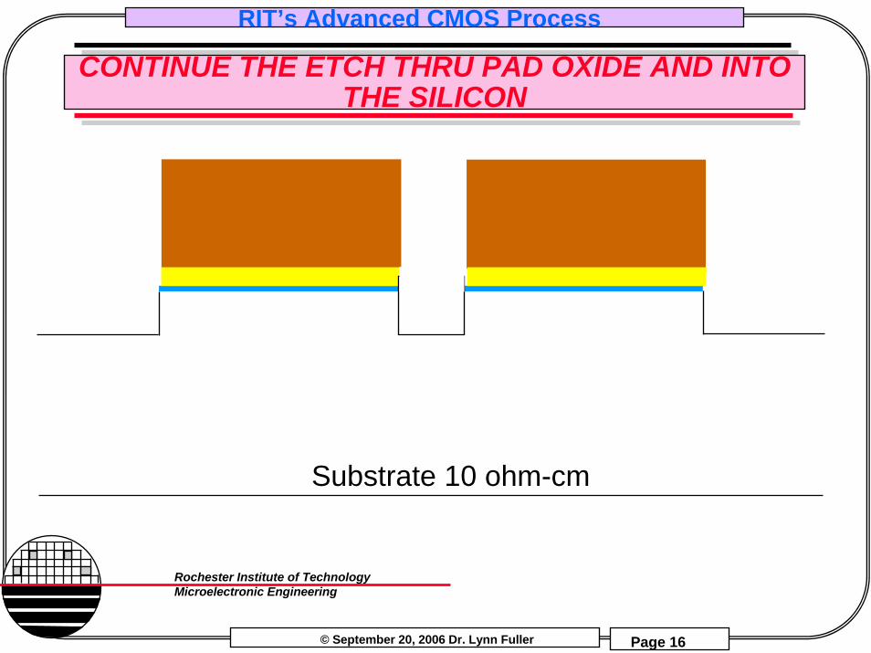
© September 20, 2006 Dr. Lynn Fuller
RIT’s Advanced CMOS Process
Page 16
Rochester Institute of TechnologyMicroelectronic Engineering
CONTINUE THE ETCH THRU PAD OXIDE AND INTO THE SILICON
Substrate 10 ohm-cm
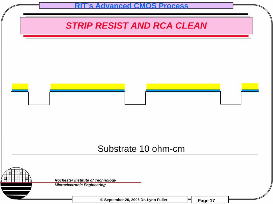
© September 20, 2006 Dr. Lynn Fuller
RIT’s Advanced CMOS Process
Page 17
Rochester Institute of TechnologyMicroelectronic Engineering
STRIP RESIST AND RCA CLEAN
Substrate 10 ohm-cm
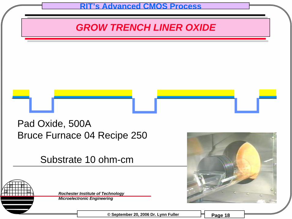
© September 20, 2006 Dr. Lynn Fuller
RIT’s Advanced CMOS Process
Page 18
Rochester Institute of TechnologyMicroelectronic Engineering
GROW TRENCH LINER OXIDE
Substrate 10 ohm-cm
Pad Oxide, 500ABruce Furnace 04 Recipe 250
© September 20, 2006 Dr. Lynn Fuller
RIT’s Advanced CMOS Process
Page 19
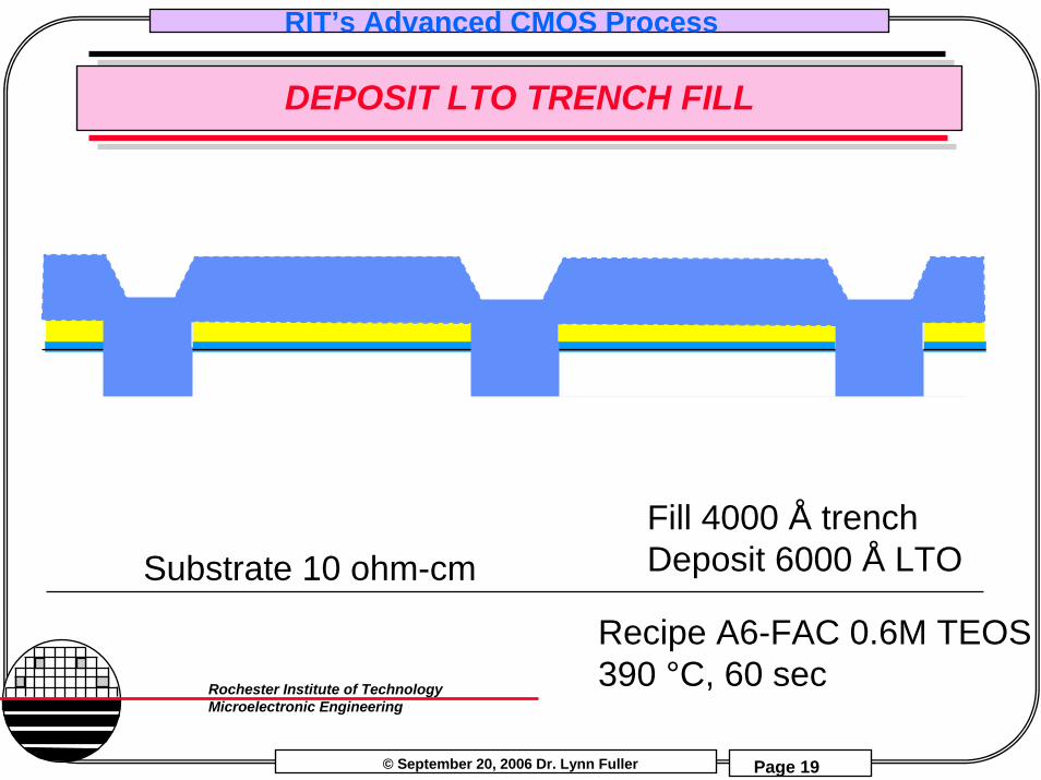
Rochester Institute of TechnologyMicroelectronic Engineering
DEPOSIT LTO TRENCH FILL
Substrate 10 ohm-cmFill 4000 Å trenchDeposit 6000 Å LTO
P-well N-well
Recipe A6-FAC 0.6M TEOS390 °C, 60 sec
© September 20, 2006 Dr. Lynn Fuller
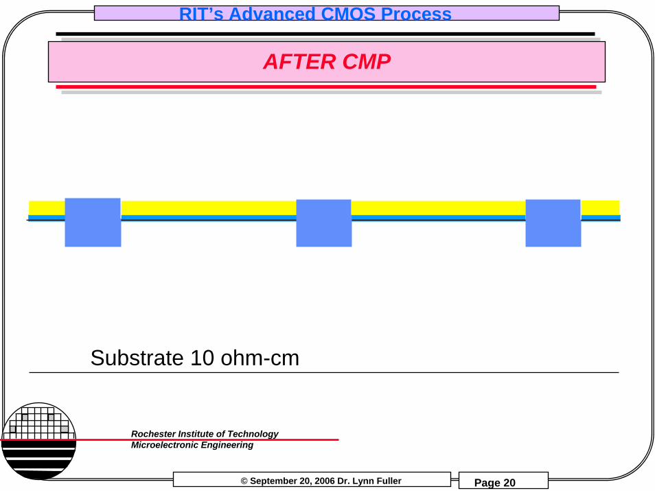
RIT’s Advanced CMOS Process
Page 20
Rochester Institute of TechnologyMicroelectronic Engineering
AFTER CMP
Substrate 10 ohm-cm
P-well N-well
© September 20, 2006 Dr. Lynn Fuller
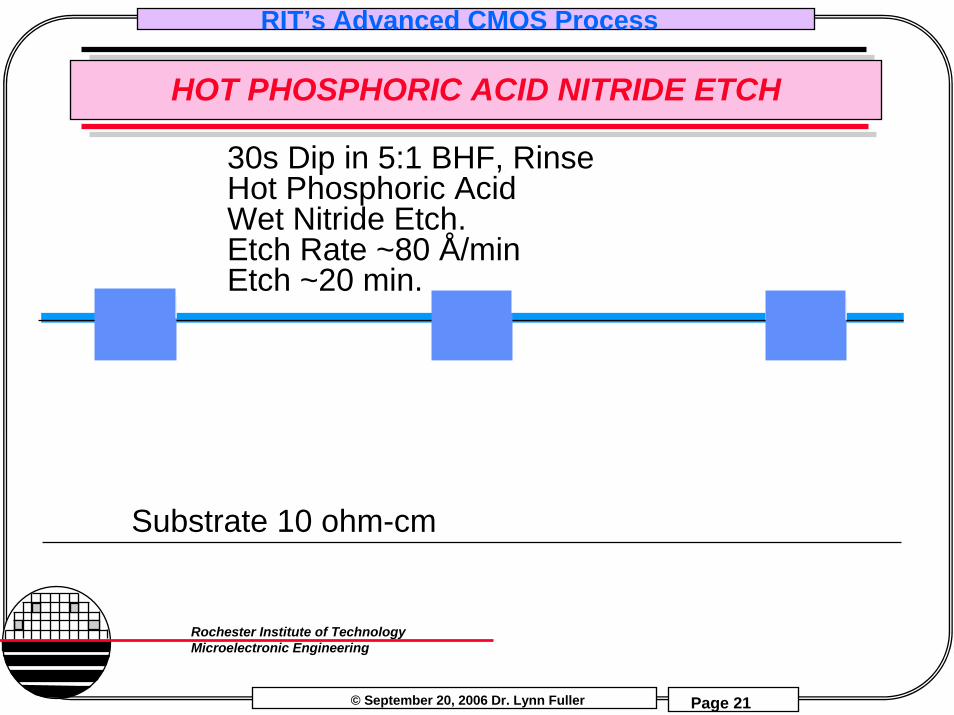
RIT’s Advanced CMOS Process
Page 21
Rochester Institute of TechnologyMicroelectronic Engineering
HOT PHOSPHORIC ACID NITRIDE ETCH
Substrate 10 ohm-cm
30s Dip in 5:1 BHF, RinseHot Phosphoric AcidWet Nitride Etch. Etch Rate ~80 Å/minEtch ~20 min.
P-well N-well
© September 20, 2006 Dr. Lynn Fuller
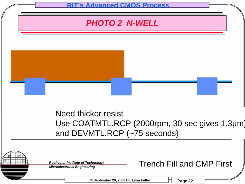
RIT’s Advanced CMOS Process
Page 22
Rochester Institute of TechnologyMicroelectronic Engineering
PHOTO 2 N-WELL
Need thicker resist Use COATMTL.RCP (2000rpm, 30 sec gives 1.3µm)and DEVMTL.RCP (~75 seconds)
Trench Fill and CMP First
© September 20, 2006 Dr. Lynn Fuller
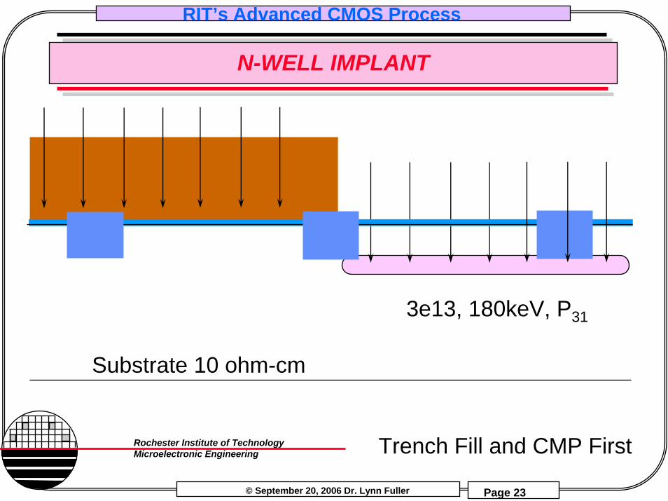
RIT’s Advanced CMOS Process
Page 23
Rochester Institute of TechnologyMicroelectronic Engineering
N-WELL IMPLANT
3e13, 180keV, P31
Substrate 10 ohm-cm
Trench Fill and CMP First
© September 20, 2006 Dr. Lynn Fuller
RIT’s Advanced CMOS Process
Page 24
Rochester Institute of TechnologyMicroelectronic Engineering
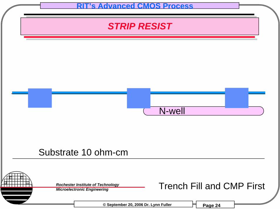
STRIP RESIST
Substrate 10 ohm-cm
N-well
Trench Fill and CMP First
© September 20, 2006 Dr. Lynn Fuller
RIT’s Advanced CMOS Process
Page 25
Rochester Institute of TechnologyMicroelectronic Engineering
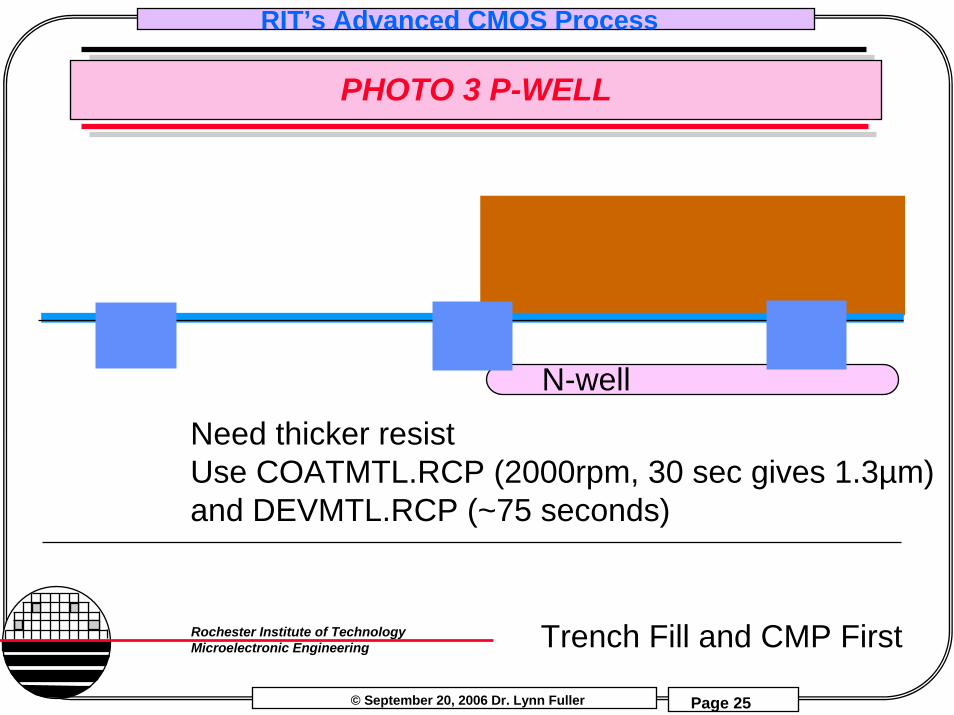
PHOTO 3 P-WELL
N-well
Need thicker resist Use COATMTL.RCP (2000rpm, 30 sec gives 1.3µm)and DEVMTL.RCP (~75 seconds)
Trench Fill and CMP First
© September 20, 2006 Dr. Lynn Fuller
RIT’s Advanced CMOS Process
Page 26
Rochester Institute of TechnologyMicroelectronic Engineering
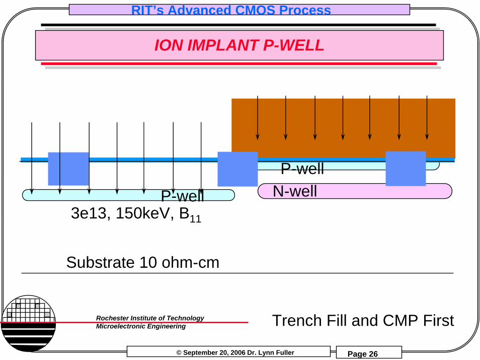
ION IMPLANT P-WELL
Substrate 10 ohm-cm
3e13, 150keV, B11
P-well N-wellP-well
Trench Fill and CMP First
© September 20, 2006 Dr. Lynn Fuller
RIT’s Advanced CMOS Process
Page 27
Rochester Institute of TechnologyMicroelectronic Engineering
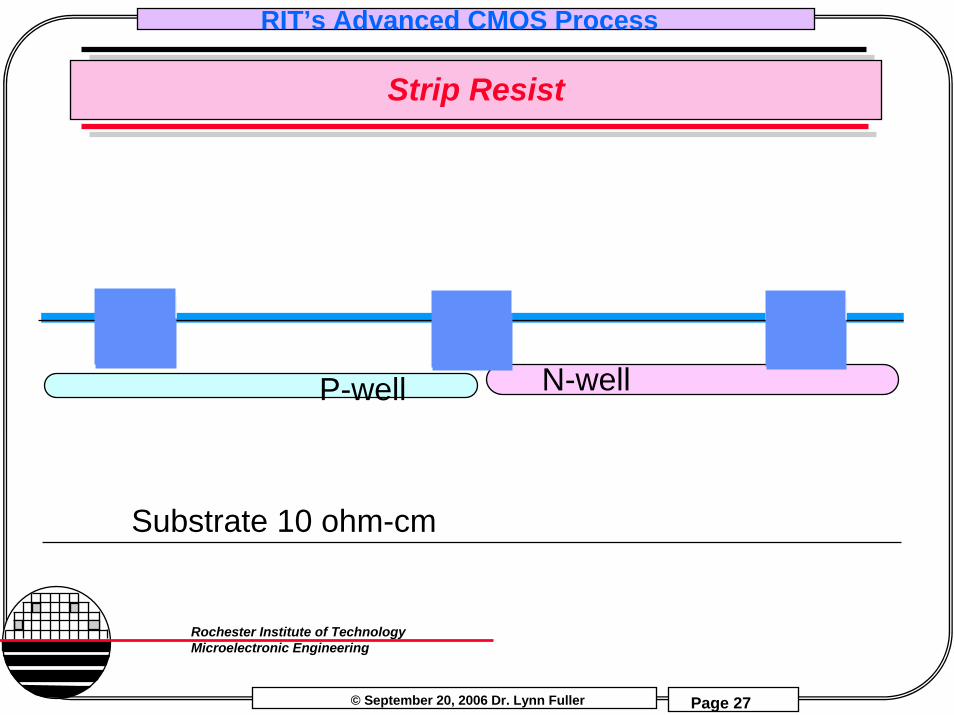
Strip Resist
Substrate 10 ohm-cm
P-well N-well
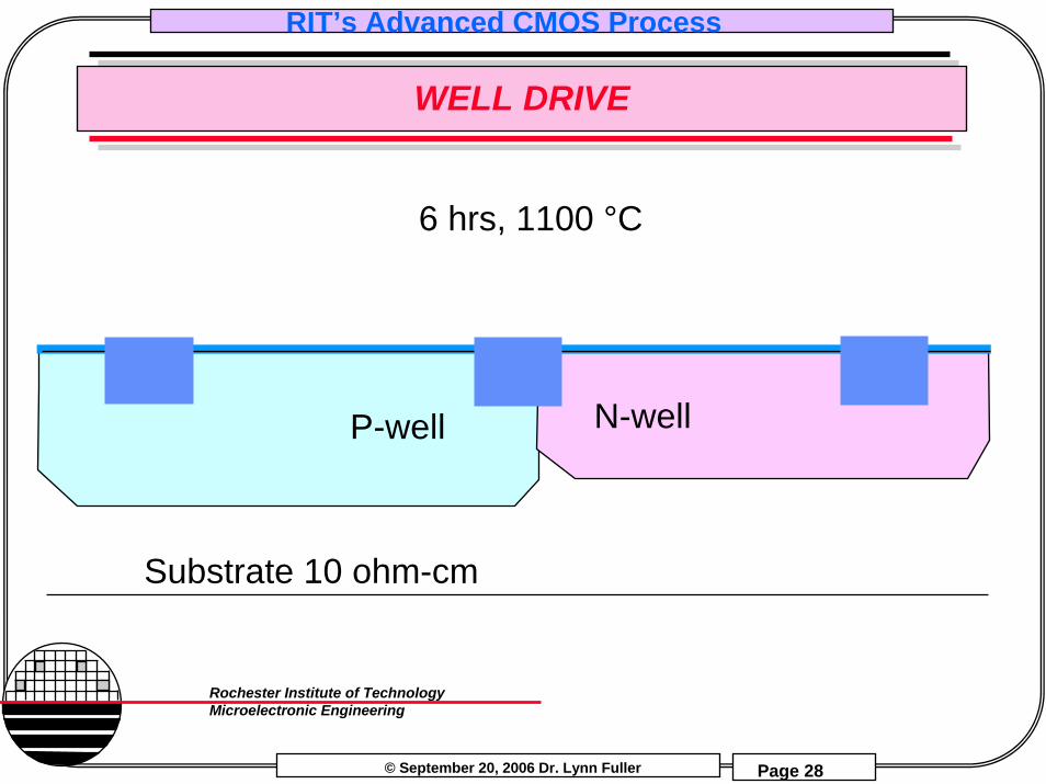
© September 20, 2006 Dr. Lynn Fuller
RIT’s Advanced CMOS Process
Page 28
Rochester Institute of TechnologyMicroelectronic Engineering
WELL DRIVE
Substrate 10 ohm-cm
P-well N-well
6 hrs, 1100 °C
© September 20, 2006 Dr. Lynn Fuller
RIT’s Advanced CMOS Process
Page 29
Rochester Institute of TechnologyMicroelectronic Engineering
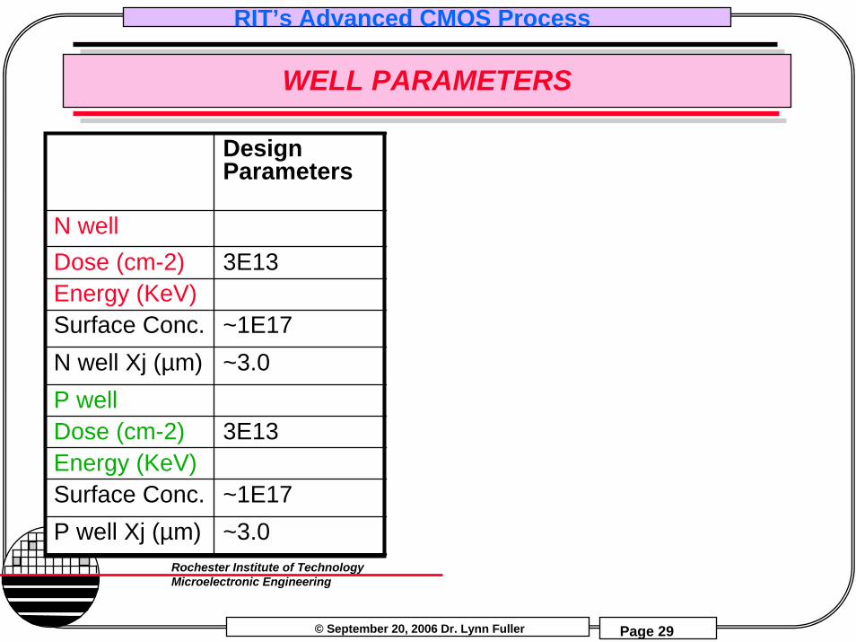
WELL PARAMETERS
Design Parameters
Trench Fill & CMP First
Implant Wells First
Implant First
N wellDose (cm-2) 3E13 3E13 3E13Energy (KeV) 180 170 Lower
Dose (cm-2) 3E13 3E13 8E13Energy (KeV) 150 80 Lower
BetterBetter
BetterBetter
Surface Conc. ~1E17 2.4E17 1.08E17N well Xj (µm) ~3.0 4.0# 3.5P well
Surface Conc. ~1E17 3.6E16 1.0E17P well Xj (µm) ~3.0 3.3 3.1

© September 20, 2006 Dr. Lynn Fuller
RIT’s Advanced CMOS Process
Page 30
Rochester Institute of TechnologyMicroelectronic Engineering
PHOTO - NMOS VT ADJUST
Substrate 10 ohm-cm
P-well N-well
© September 20, 2006 Dr. Lynn Fuller
RIT’s Advanced CMOS Process
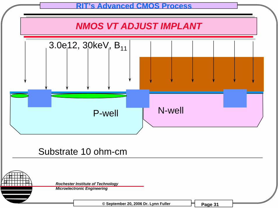
Page 31
Rochester Institute of TechnologyMicroelectronic Engineering
NMOS VT ADJUST IMPLANT
3.0e12, 30keV, B11
Substrate 10 ohm-cm
P-well N-well
© September 20, 2006 Dr. Lynn Fuller
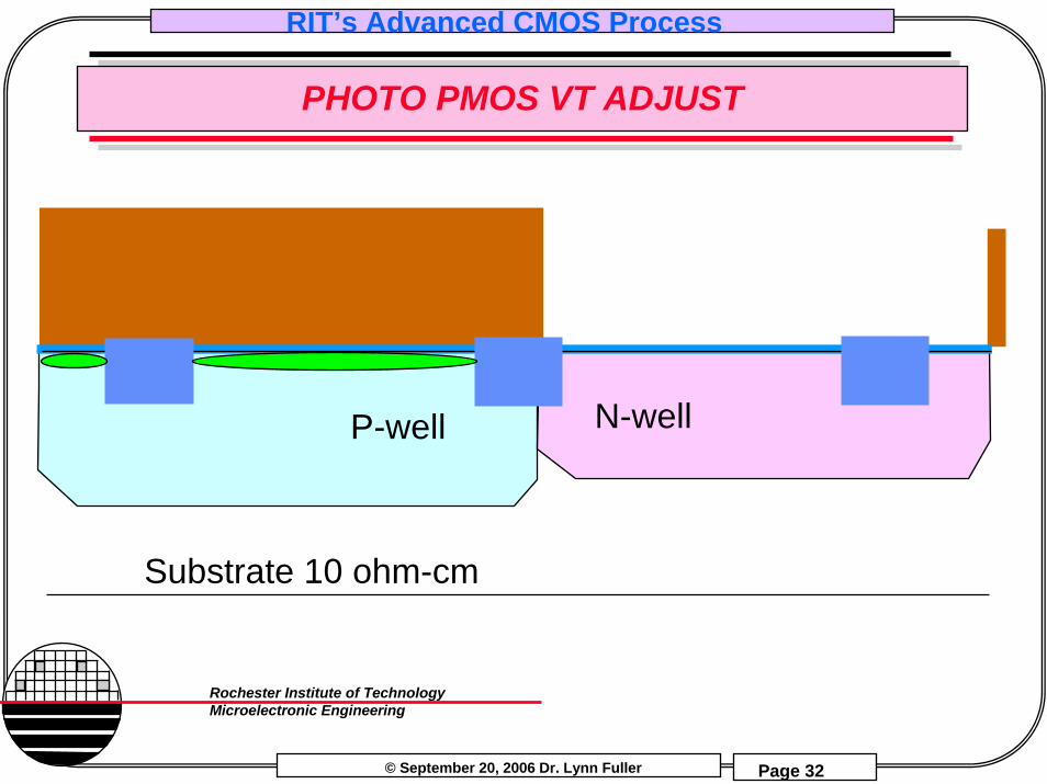
RIT’s Advanced CMOS Process
Page 32
Rochester Institute of TechnologyMicroelectronic Engineering
PHOTO PMOS VT ADJUST
Substrate 10 ohm-cm
P-well N-well
© September 20, 2006 Dr. Lynn Fuller
RIT’s Advanced CMOS Process
Page 33
Rochester Institute of TechnologyMicroelectronic Engineering
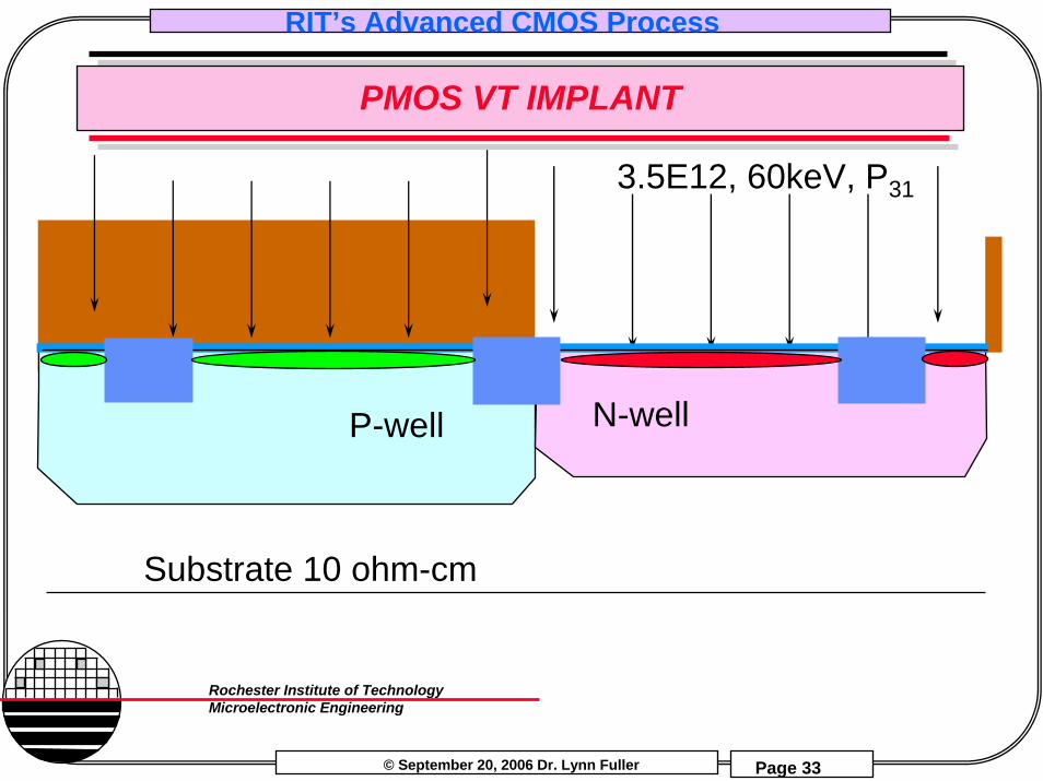
PMOS VT IMPLANT
3.5E12, 60keV, P31
Substrate 10 ohm-cm
P-well N-well
© September 20, 2006 Dr. Lynn Fuller
RIT’s Advanced CMOS Process
Page 34
Rochester Institute of TechnologyMicroelectronic Engineering
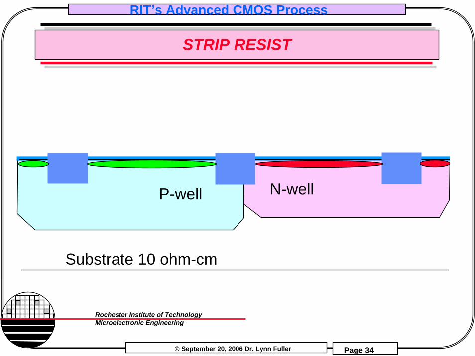
STRIP RESIST
Substrate 10 ohm-cm
P-well N-well
© September 20, 2006 Dr. Lynn Fuller
RIT’s Advanced CMOS Process
Page 35
Rochester Institute of TechnologyMicroelectronic Engineering
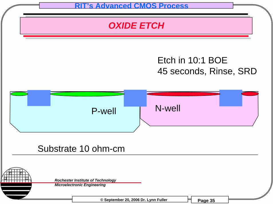
OXIDE ETCH
Substrate 10 ohm-cm
P-well N-well
Etch in 10:1 BOE45 seconds, Rinse, SRD
© September 20, 2006 Dr. Lynn Fuller
RIT’s Advanced CMOS Process
Page 36
Rochester Institute of TechnologyMicroelectronic Engineering
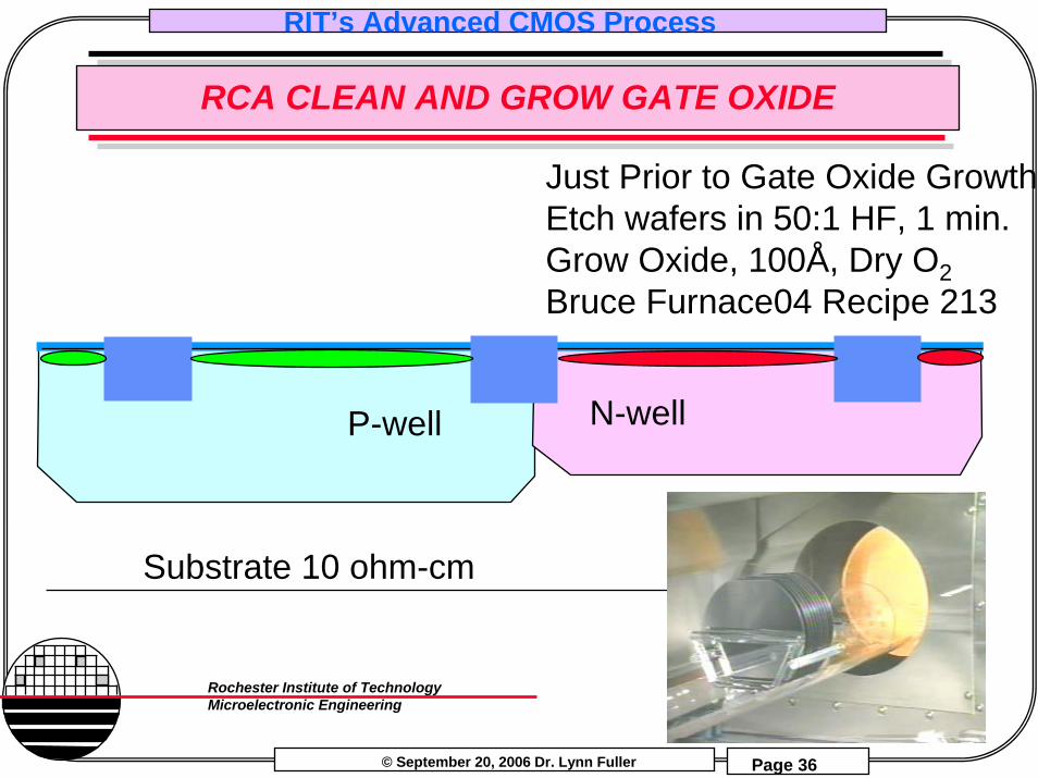
RCA CLEAN AND GROW GATE OXIDE
Just Prior to Gate Oxide GrowthEtch wafers in 50:1 HF, 1 min.Grow Oxide, 100Å, Dry O2Bruce Furnace04 Recipe 213
Substrate 10 ohm-cm
P-well N-well
© September 20, 2006 Dr. Lynn Fuller
RIT’s Advanced CMOS Process
Page 37
Rochester Institute of TechnologyMicroelectronic Engineering
INCORPORATING NITROGEN IN THIN GATE OXIDES
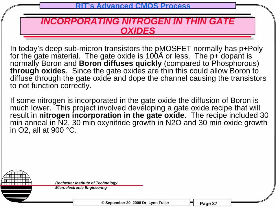
In today’s deep sub-micron transistors the pMOSFET normally has p+Poly for the gate material. The gate oxide is 100Å or less. The p+ dopant is normally Boron and Boron diffuses quickly (compared to Phosphorous) through oxides. Since the gate oxides are thin this could allow Boron to diffuse through the gate oxide and dope the channel causing the transistors to not function correctly.
If some nitrogen is incorporated in the gate oxide the diffusion of Boron is much lower. This project involved developing a gate oxide recipe that will result in nitrogen incorporation in the gate oxide. The recipe included 30 min anneal in N2, 30 min oxynitride growth in N2O and 30 min oxide growth in O2, all at 900 °C.
© September 20, 2006 Dr. Lynn Fuller
RIT’s Advanced CMOS Process
Page 38
Rochester Institute of TechnologyMicroelectronic Engineering
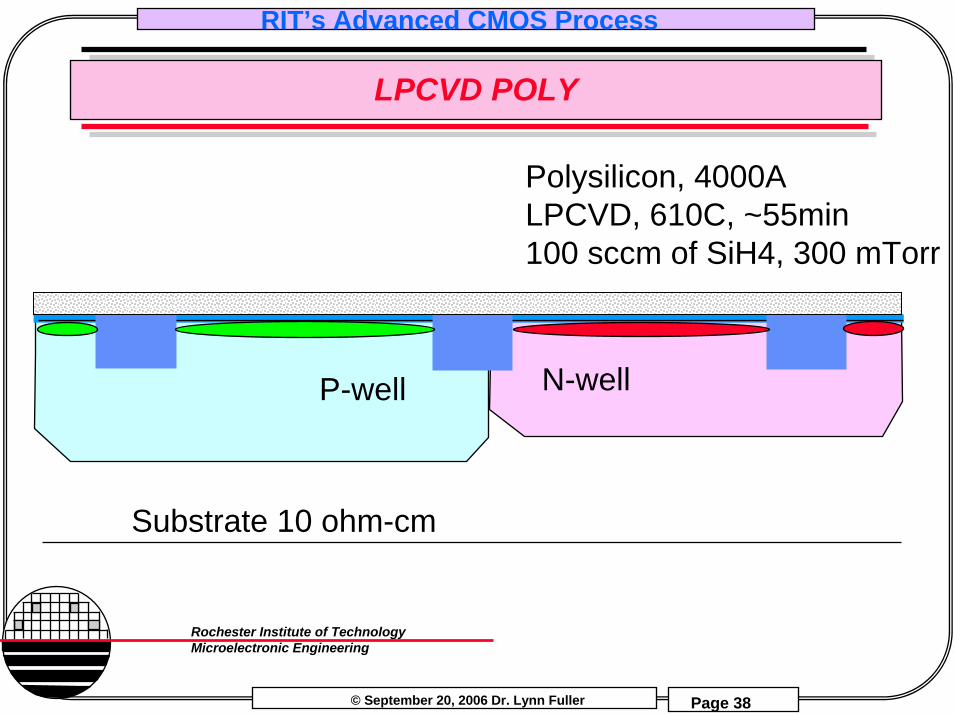
LPCVD POLY
Polysilicon, 4000ALPCVD, 610C, ~55min100 sccm of SiH4, 300 mTorr
Substrate 10 ohm-cm
P-well N-well
© September 20, 2006 Dr. Lynn Fuller
RIT’s Advanced CMOS Process
Page 39
Rochester Institute of TechnologyMicroelectronic Engineering
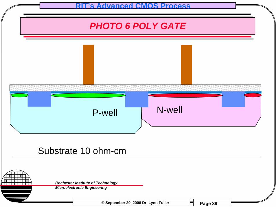
PHOTO 6 POLY GATE
Substrate 10 ohm-cm
P-well N-well

© September 20, 2006 Dr. Lynn Fuller
RIT’s Advanced CMOS Process
Page 40
Rochester Institute of TechnologyMicroelectronic Engineering
POLY ETCH
Substrate 10 ohm-cm
P-well N-well
© September 20, 2006 Dr. Lynn Fuller
RIT’s Advanced CMOS Process
Page 41
Rochester Institute of TechnologyMicroelectronic Engineering
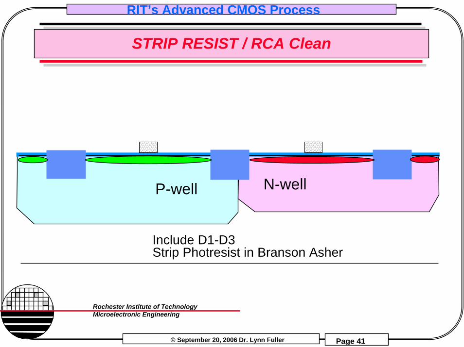
STRIP RESIST / RCA Clean
P-well N-well
Include D1-D3Strip Photresist in Branson Asher
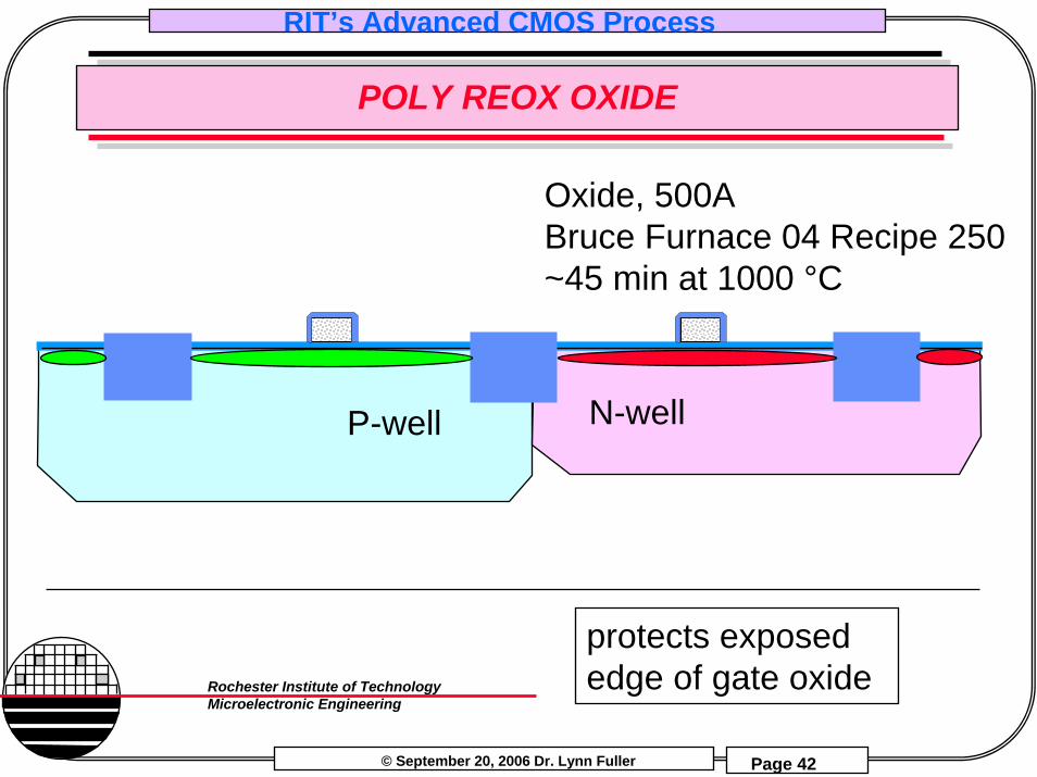
© September 20, 2006 Dr. Lynn Fuller
RIT’s Advanced CMOS Process
Page 42
Rochester Institute of TechnologyMicroelectronic Engineering
POLY REOX OXIDE
P-well N-well
Oxide, 500ABruce Furnace 04 Recipe 250~45 min at 1000 °C
protects exposed edge of gate oxide

© September 20, 2006 Dr. Lynn Fuller
RIT’s Advanced CMOS Process
Page 43
Rochester Institute of TechnologyMicroelectronic Engineering
PHOTO 7 LDD P-TYPE IMPLANT
Substrate 10 ohm-cm
P-well N-well
© September 20, 2006 Dr. Lynn Fuller
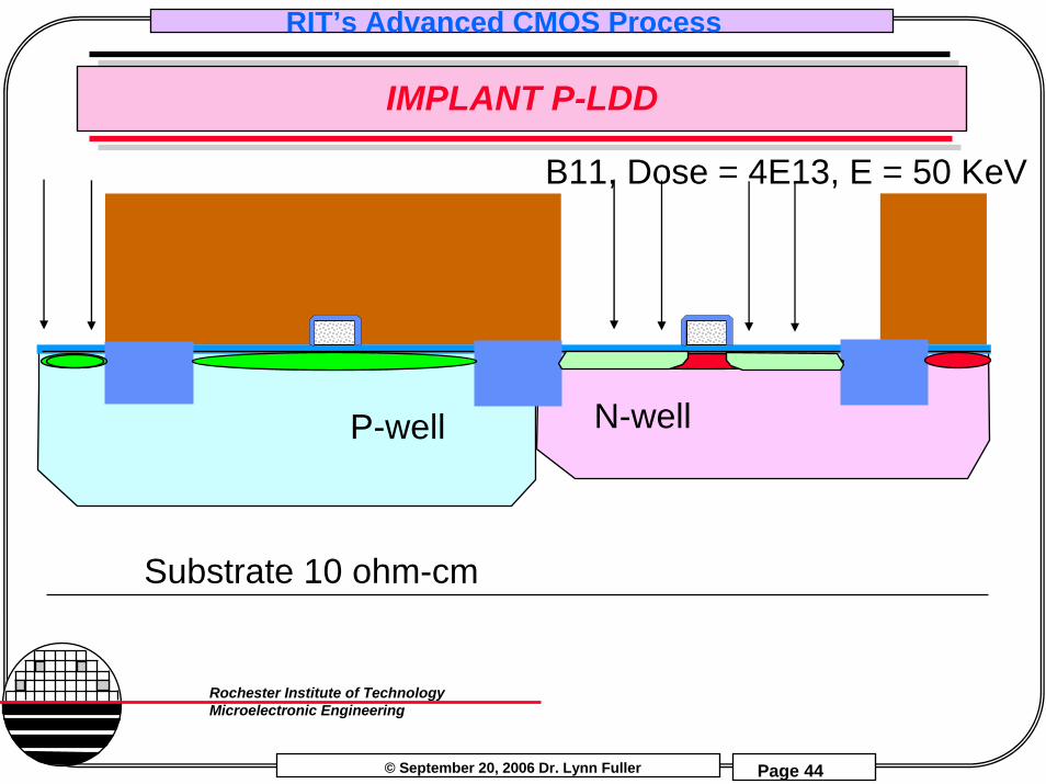
RIT’s Advanced CMOS Process
Page 44
Rochester Institute of TechnologyMicroelectronic Engineering
IMPLANT P-LDD
Substrate 10 ohm-cm
P-well N-well
B11, Dose = 4E13, E = 50 KeV
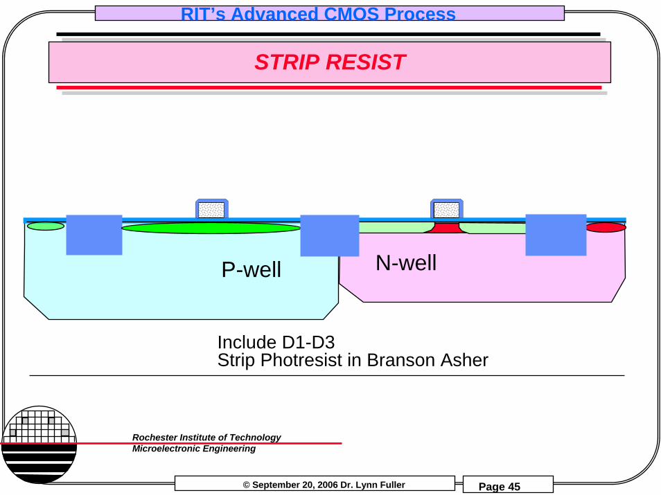
© September 20, 2006 Dr. Lynn Fuller
RIT’s Advanced CMOS Process
Page 45
Rochester Institute of TechnologyMicroelectronic Engineering
STRIP RESIST
P-well N-well
Include D1-D3Strip Photresist in Branson Asher

© September 20, 2006 Dr. Lynn Fuller
RIT’s Advanced CMOS Process
Page 46
Rochester Institute of TechnologyMicroelectronic Engineering
PHOTO 8 LDD N-TYPE IMPLANT
Substrate 10 ohm-cm
P-well N-well

© September 20, 2006 Dr. Lynn Fuller
RIT’s Advanced CMOS Process
Page 47
Rochester Institute of TechnologyMicroelectronic Engineering
IMPLANT N-LDD
Substrate 10 ohm-cm
P-well N-well
P31, Dose = 4E13, E = 60 KeV
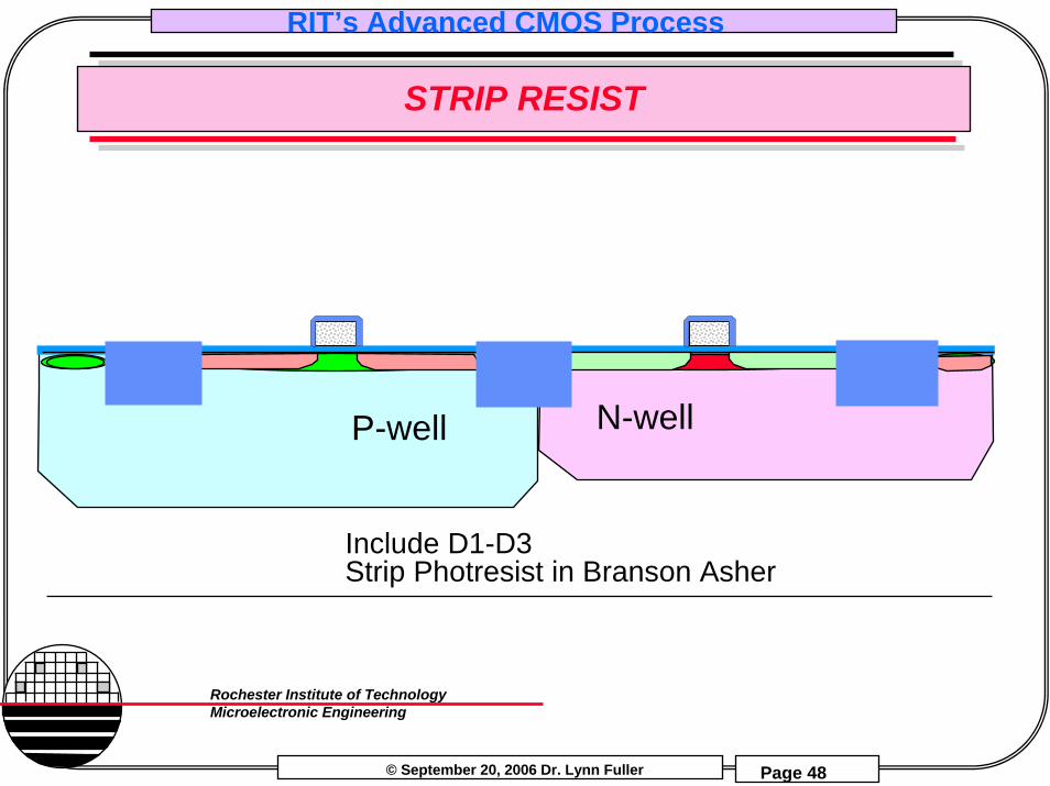
© September 20, 2006 Dr. Lynn Fuller
RIT’s Advanced CMOS Process
Page 48
Rochester Institute of TechnologyMicroelectronic Engineering
STRIP RESIST
P-well N-well
Include D1-D3Strip Photresist in Branson Asher
© September 20, 2006 Dr. Lynn Fuller
RIT’s Advanced CMOS Process
Page 49
Rochester Institute of TechnologyMicroelectronic Engineering
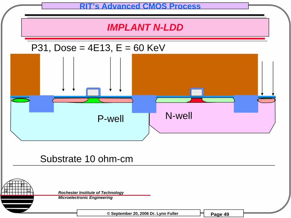
IMPLANT N-LDD
Substrate 10 ohm-cm
P-well N-well
P31, Dose = 4E13, E = 60 KeV

© September 20, 2006 Dr. Lynn Fuller
RIT’s Advanced CMOS Process
Page 50
Rochester Institute of TechnologyMicroelectronic Engineering
STRIP RESIST
P-well N-well
Include D1-D3Strip Photresist in Branson Asher
© September 20, 2006 Dr. Lynn Fuller
RIT’s Advanced CMOS Process
Page 51
Rochester Institute of TechnologyMicroelectronic Engineering
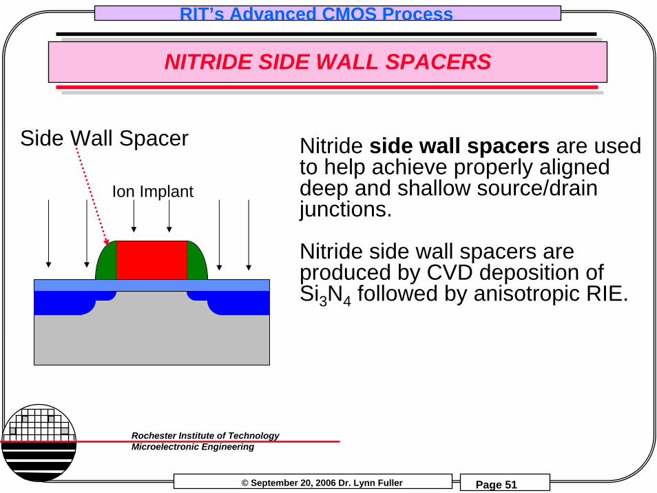
NITRIDE SIDE WALL SPACERS
Nitride side wall spacers are used to help achieve properly aligned deep and shallow source/drain junctions.
Nitride side wall spacers are produced by CVD deposition of Si3N4 followed by anisotropic RIE.
Side Wall Spacer
Ion Implant
© September 20, 2006 Dr. Lynn Fuller
RIT’s Advanced CMOS Process
Page 52
Rochester Institute of TechnologyMicroelectronic Engineering
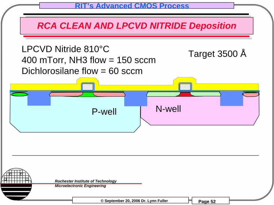
RCA CLEAN AND LPCVD NITRIDE Deposition
Target 3500 Å
P-well N-well
LPCVD Nitride 810°C400 mTorr, NH3 flow = 150 sccmDichlorosilane flow = 60 sccm
© September 20, 2006 Dr. Lynn Fuller
RIT’s Advanced CMOS Process
Page 53
Rochester Institute of TechnologyMicroelectronic Engineering
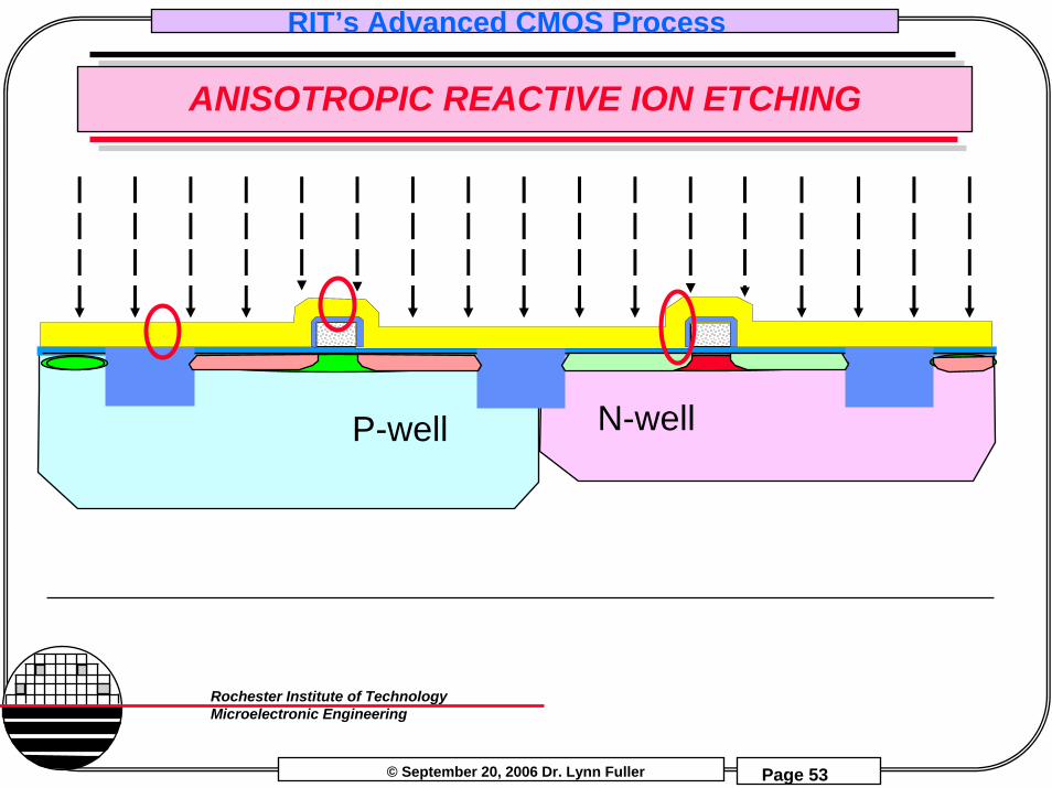
ANISOTROPIC REACTIVE ION ETCHING
P-well N-well
© September 20, 2006 Dr. Lynn Fuller
RIT’s Advanced CMOS Process
Page 54
Rochester Institute of TechnologyMicroelectronic Engineering
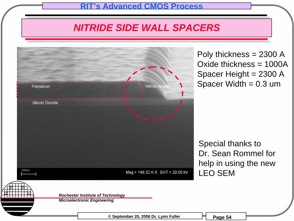
NITRIDE SIDE WALL SPACERS
Poly thickness = 2300 AOxide thickness = 1000ASpacer Height = 2300 ASpacer Width = 0.3 um
Special thanks toDr. Sean Rommel forhelp in using the newLEO SEM
© September 20, 2006 Dr. Lynn Fuller
RIT’s Advanced CMOS Process
Page 55
Rochester Institute of TechnologyMicroelectronic Engineering
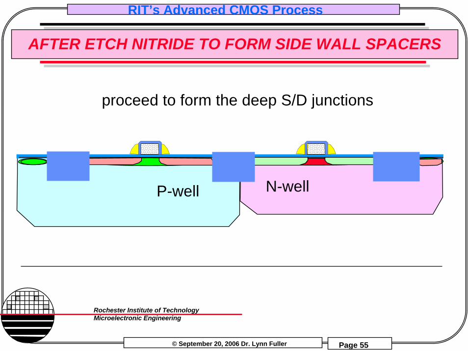
AFTER ETCH NITRIDE TO FORM SIDE WALL SPACERS
P-well N-well
proceed to form the deep S/D junctions
© September 20, 2006 Dr. Lynn Fuller
RIT’s Advanced CMOS Process
Page 56
Rochester Institute of TechnologyMicroelectronic Engineering
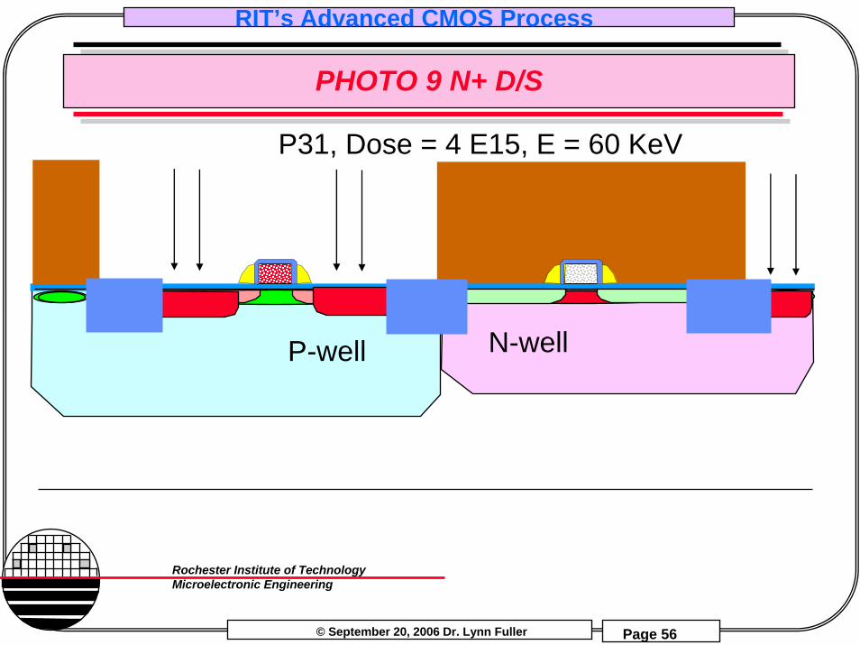
PHOTO 9 N+ D/S
P-well N-well
P31, Dose = 4 E15, E = 60 KeV
© September 20, 2006 Dr. Lynn Fuller
RIT’s Advanced CMOS Process
Page 57
Rochester Institute of TechnologyMicroelectronic Engineering
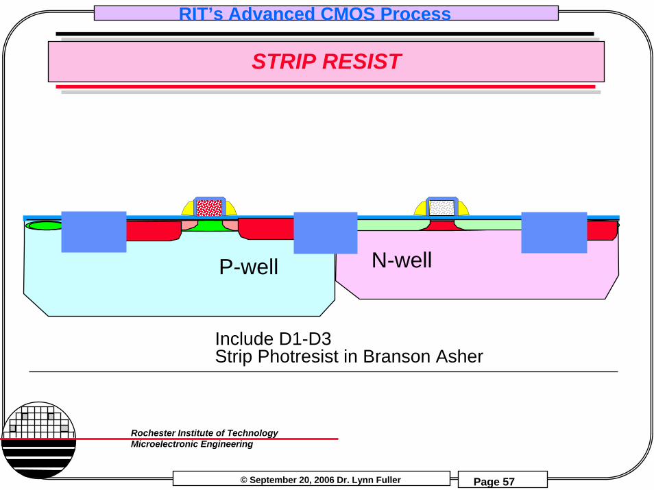
STRIP RESIST
P-well N-well
Include D1-D3Strip Photresist in Branson Asher
© September 20, 2006 Dr. Lynn Fuller
RIT’s Advanced CMOS Process
Page 58
Rochester Institute of TechnologyMicroelectronic Engineering
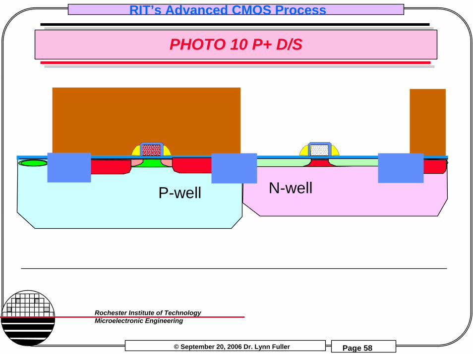
PHOTO 10 P+ D/S
P-well N-well
© September 20, 2006 Dr. Lynn Fuller
RIT’s Advanced CMOS Process
Page 59
Rochester Institute of TechnologyMicroelectronic Engineering
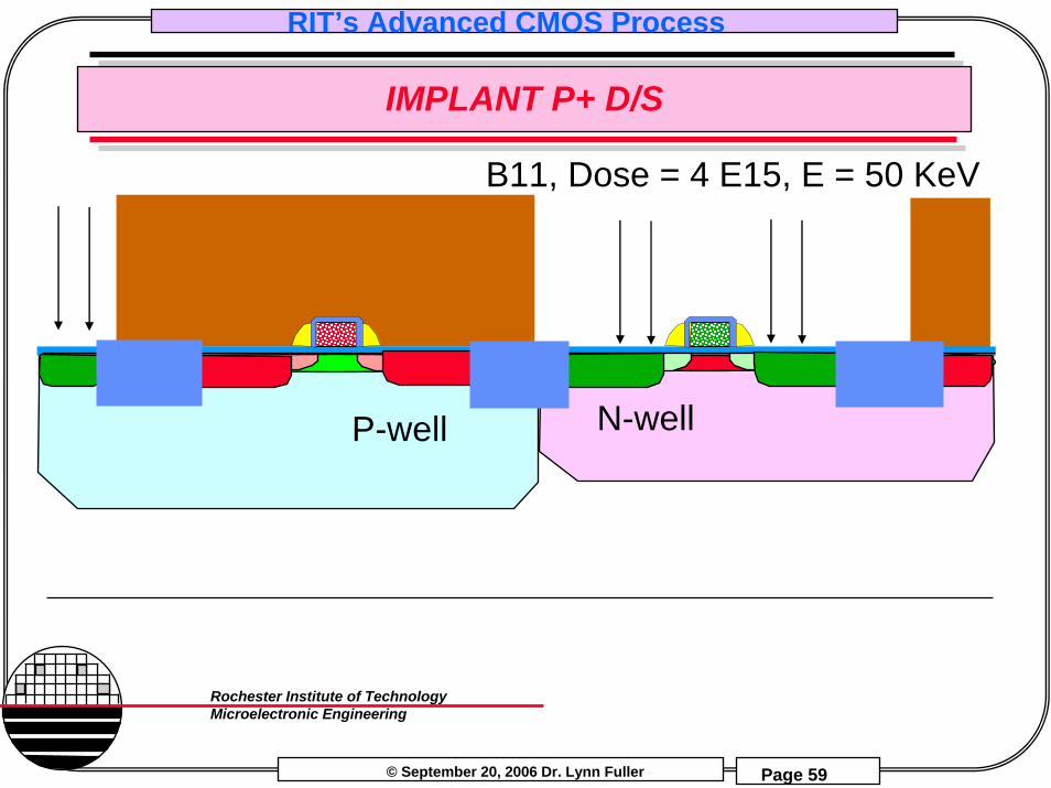
IMPLANT P+ D/S
B11, Dose = 4 E15, E = 50 KeV
P-well N-well
© September 20, 2006 Dr. Lynn Fuller
RIT’s Advanced CMOS Process
Page 60
Rochester Institute of TechnologyMicroelectronic Engineering
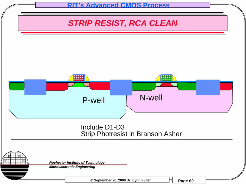
STRIP RESIST, RCA CLEAN
P-well N-well
Include D1-D3Strip Photresist in Branson Asher
© September 20, 2006 Dr. Lynn Fuller
RIT’s Advanced CMOS Process
Page 61
Rochester Institute of TechnologyMicroelectronic Engineering
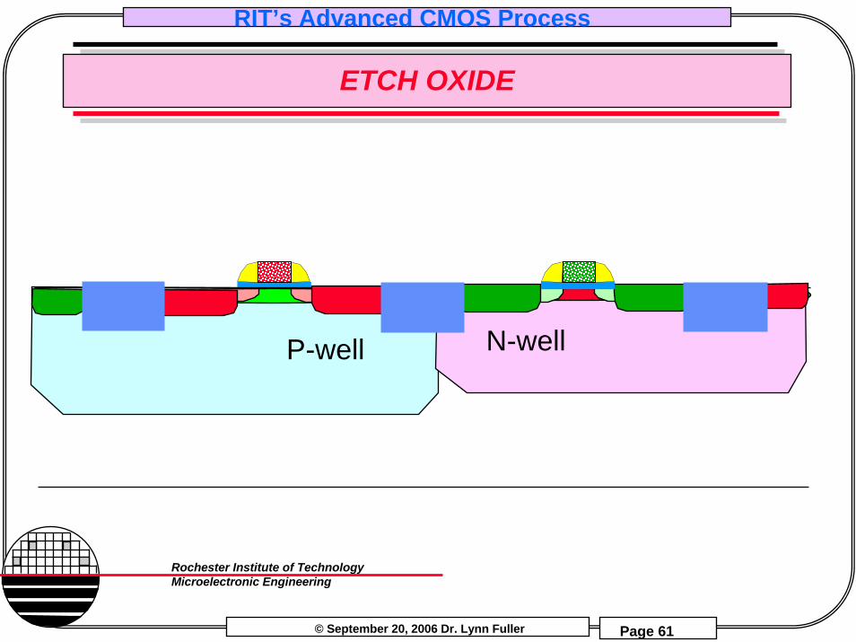
ETCH OXIDE
P-well N-well
© September 20, 2006 Dr. Lynn Fuller
RIT’s Advanced CMOS Process
Page 62
Rochester Institute of TechnologyMicroelectronic Engineering
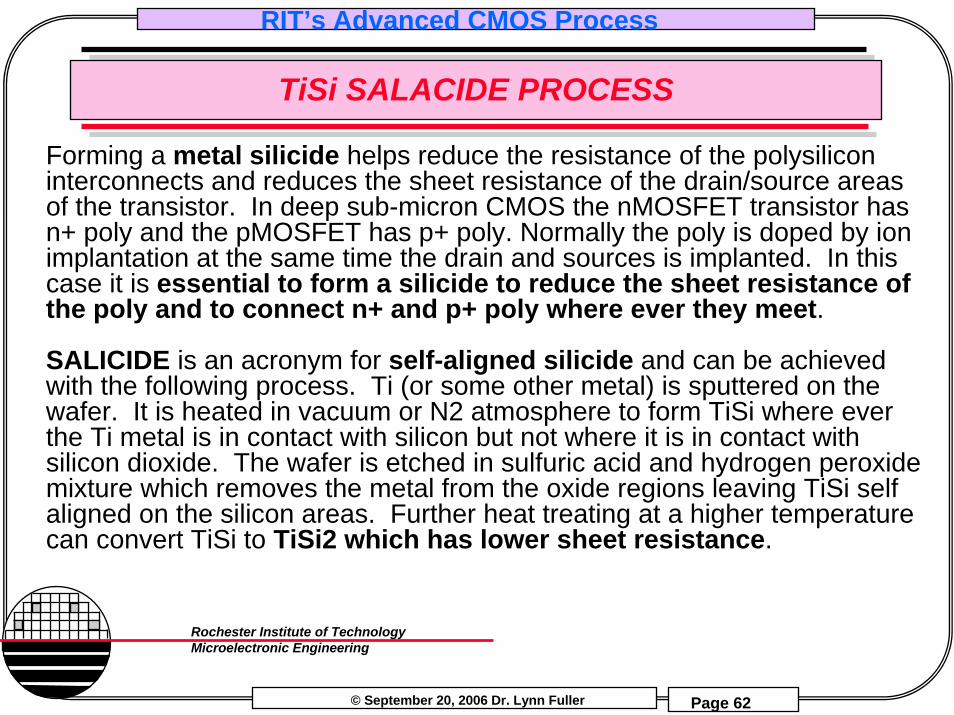
TiSi SALACIDE PROCESS
Forming a metal silicide helps reduce the resistance of the polysilicon interconnects and reduces the sheet resistance of the drain/source areas of the transistor. In deep sub-micron CMOS the nMOSFET transistor has n+ poly and the pMOSFET has p+ poly. Normally the poly is doped by ion implantation at the same time the drain and sources is implanted. In this case it is essential to form a silicide to reduce the sheet resistance of the poly and to connect n+ and p+ poly where ever they meet.
SALICIDE is an acronym for self-aligned silicide and can be achieved with the following process. Ti (or some other metal) is sputtered on the wafer. It is heated in vacuum or N2 atmosphere to form TiSi where ever the Ti metal is in contact with silicon but not where it is in contact with silicon dioxide. The wafer is etched in sulfuric acid and hydrogen peroxide mixture which removes the metal from the oxide regions leaving TiSi self aligned on the silicon areas. Further heat treating at a higher temperature can convert TiSi to TiSi2 which has lower sheet resistance.
© September 20, 2006 Dr. Lynn Fuller
RIT’s Advanced CMOS Process
Page 63
Rochester Institute of TechnologyMicroelectronic Engineering
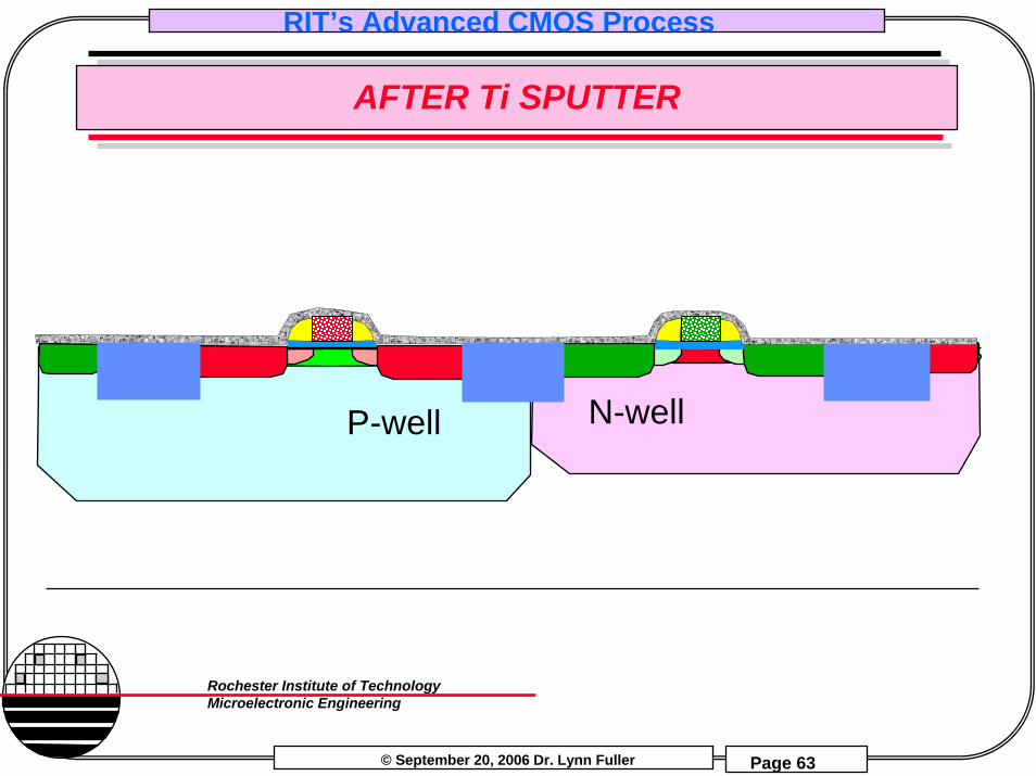
AFTER Ti SPUTTER
P-well N-well
© September 20, 2006 Dr. Lynn Fuller
RIT’s Advanced CMOS Process
Page 64
Rochester Institute of TechnologyMicroelectronic Engineering
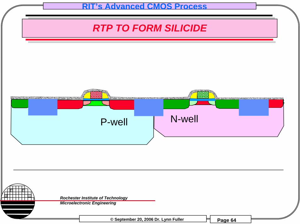
RTP TO FORM SILICIDE
P-well N-well
© September 20, 2006 Dr. Lynn Fuller
RIT’s Advanced CMOS Process
Page 65
Rochester Institute of TechnologyMicroelectronic Engineering
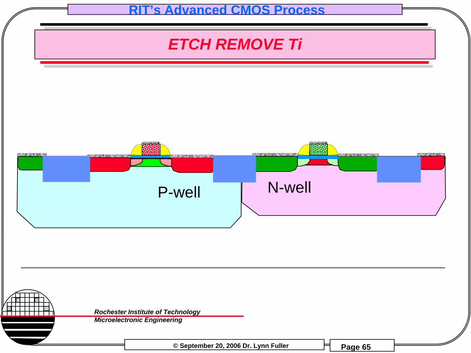
ETCH REMOVE Ti
P-well N-well
© September 20, 2006 Dr. Lynn Fuller
RIT’s Advanced CMOS Process
Page 66
Rochester Institute of TechnologyMicroelectronic Engineering
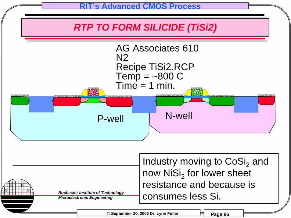
RTP TO FORM SILICIDE (TiSi2)
P-well N-well
AG Associates 610N2 Recipe TiSi2.RCPTemp = ~800 CTime = 1 min.
Industry moving to CoSi2 and now NiSi2 for lower sheet resistance and because is consumes less Si.
© September 20, 2006 Dr. Lynn Fuller
RIT’s Advanced CMOS Process
Page 67
Rochester Institute of TechnologyMicroelectronic Engineering
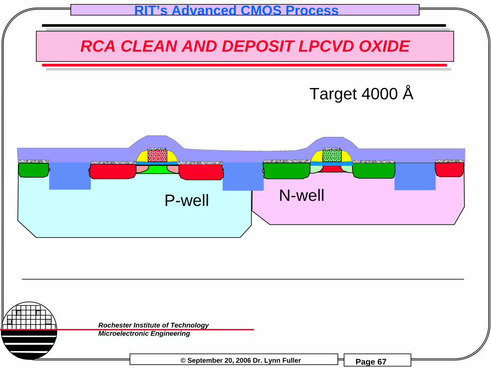
RCA CLEAN AND DEPOSIT LPCVD OXIDE
Target 4000 Å
P-well N-well
© September 20, 2006 Dr. Lynn Fuller
RIT’s Advanced CMOS Process
Page 68
Rochester Institute of TechnologyMicroelectronic Engineering
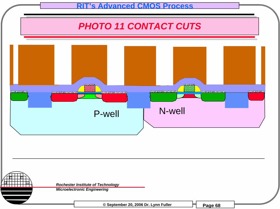
PHOTO 11 CONTACT CUTS
P-well N-well
© September 20, 2006 Dr. Lynn Fuller
RIT’s Advanced CMOS Process
Page 69
Rochester Institute of TechnologyMicroelectronic Engineering
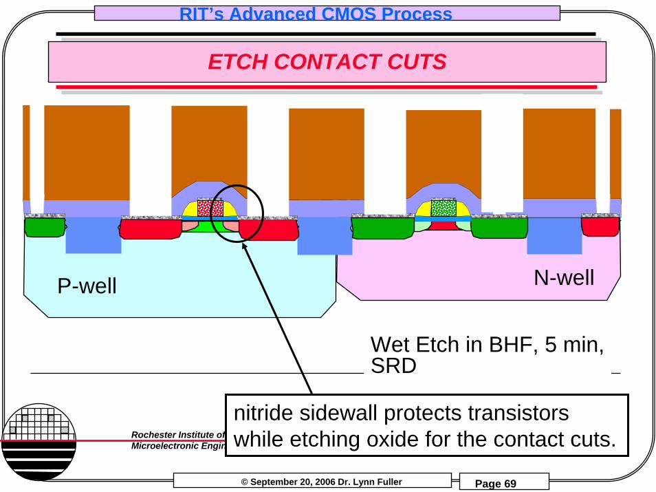
ETCH CONTACT CUTS
P-well N-well
Wet Etch in BHF, 5 min,SRD
nitride sidewall protects transistors while etching oxide for the contact cuts.
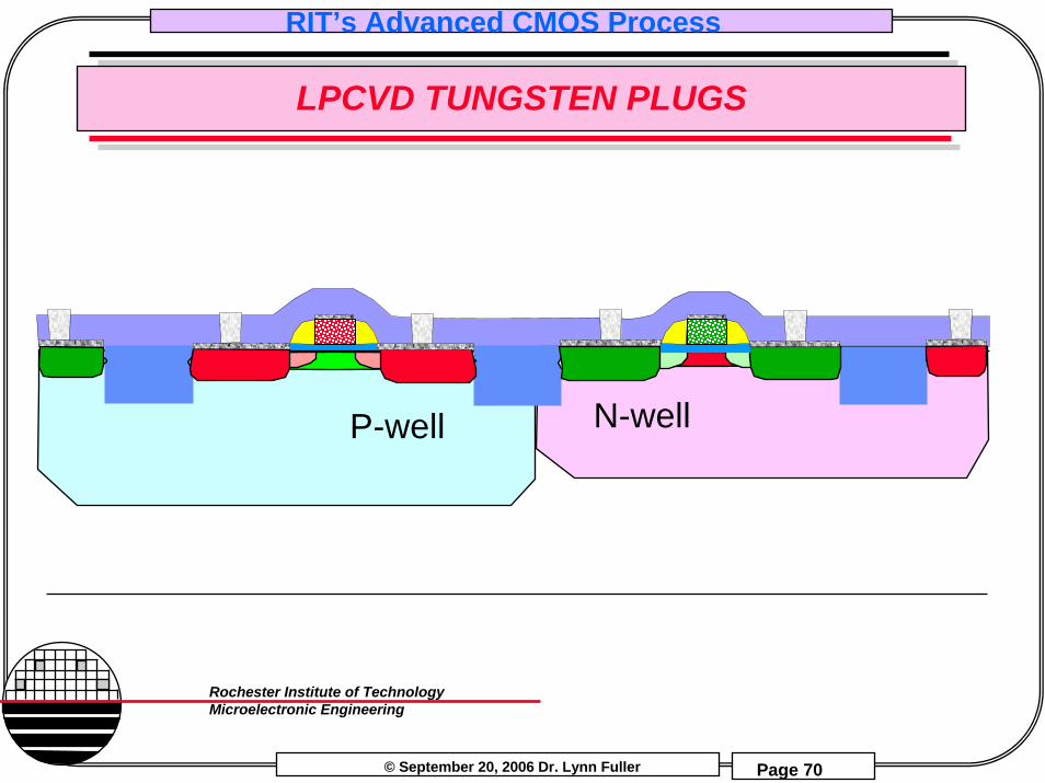
© September 20, 2006 Dr. Lynn Fuller
RIT’s Advanced CMOS Process
Page 70
Rochester Institute of TechnologyMicroelectronic Engineering
LPCVD TUNGSTEN PLUGS
P-well N-well
© September 20, 2006 Dr. Lynn Fuller
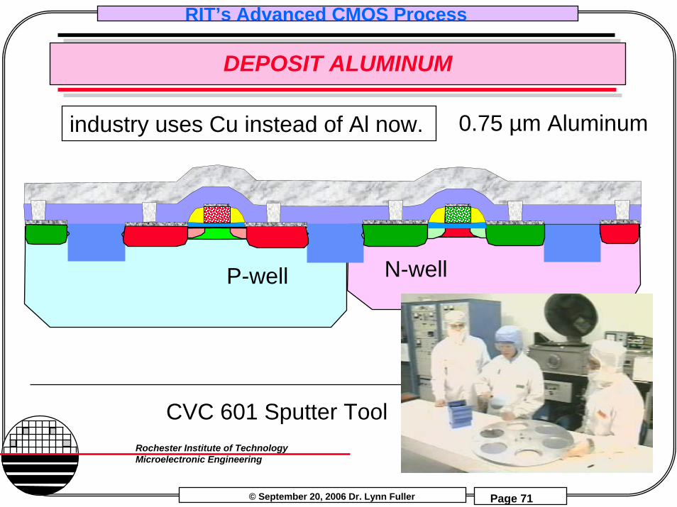
RIT’s Advanced CMOS Process
Page 71
Rochester Institute of TechnologyMicroelectronic Engineering
DEPOSIT ALUMINUM
0.75 µm Aluminum
CVC 601 Sputter Tool
P-well N-well
industry uses Cu instead of Al now.
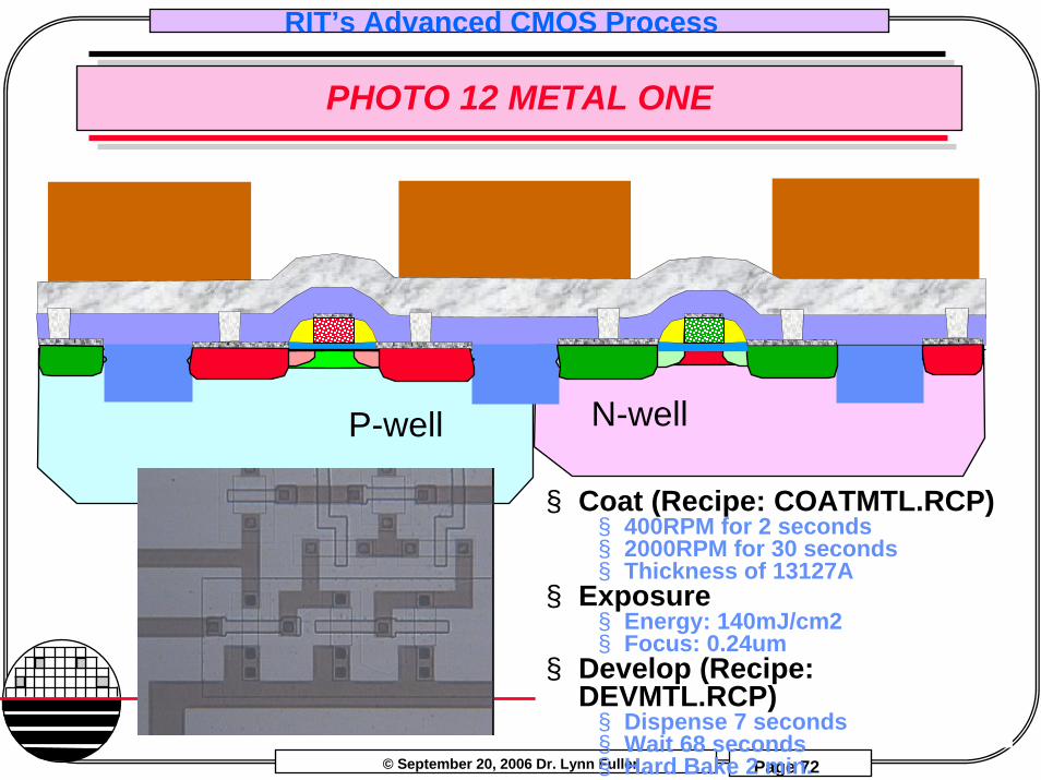
© September 20, 2006 Dr. Lynn Fuller
RIT’s Advanced CMOS Process
Page 72
Rochester Institute of TechnologyMicroelectronic Engineering
PHOTO 12 METAL ONE
P-well N-well
§ Coat (Recipe: COATMTL.RCP)§ 400RPM for 2 seconds§ 2000RPM for 30 seconds§ Thickness of 13127A
§ Exposure§ Energy: 140mJ/cm2§ Focus: 0.24um
§ Develop (Recipe: DEVMTL.RCP)
§ Dispense 7 seconds§ Wait 68 seconds§ Hard Bake 2 min.
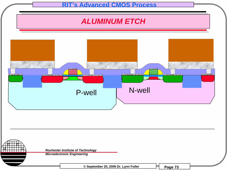
© September 20, 2006 Dr. Lynn Fuller
RIT’s Advanced CMOS Process
Page 73
Rochester Institute of TechnologyMicroelectronic Engineering
ALUMINUM ETCH
P-well N-well
© September 20, 2006 Dr. Lynn Fuller
RIT’s Advanced CMOS Process
Page 74
Rochester Institute of TechnologyMicroelectronic Engineering
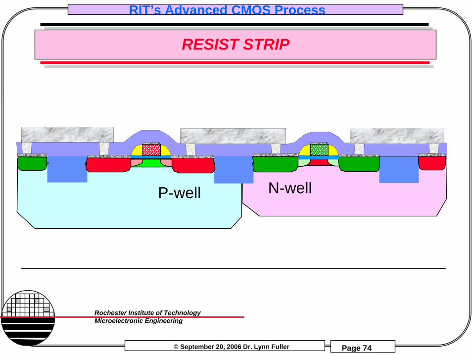
RESIST STRIP
P-well N-well
© September 20, 2006 Dr. Lynn Fuller
RIT’s Advanced CMOS Process
Page 75
Rochester Institute of TechnologyMicroelectronic Engineering
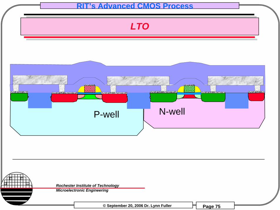
LTO
P-well N-well
© September 20, 2006 Dr. Lynn Fuller
RIT’s Advanced CMOS Process
Page 76
Rochester Institute of TechnologyMicroelectronic Engineering
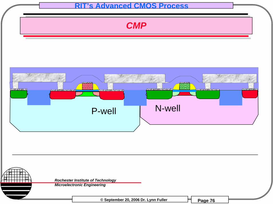
CMP
P-well N-well
© September 20, 2006 Dr. Lynn Fuller
RIT’s Advanced CMOS Process
Page 77
Rochester Institute of TechnologyMicroelectronic Engineering
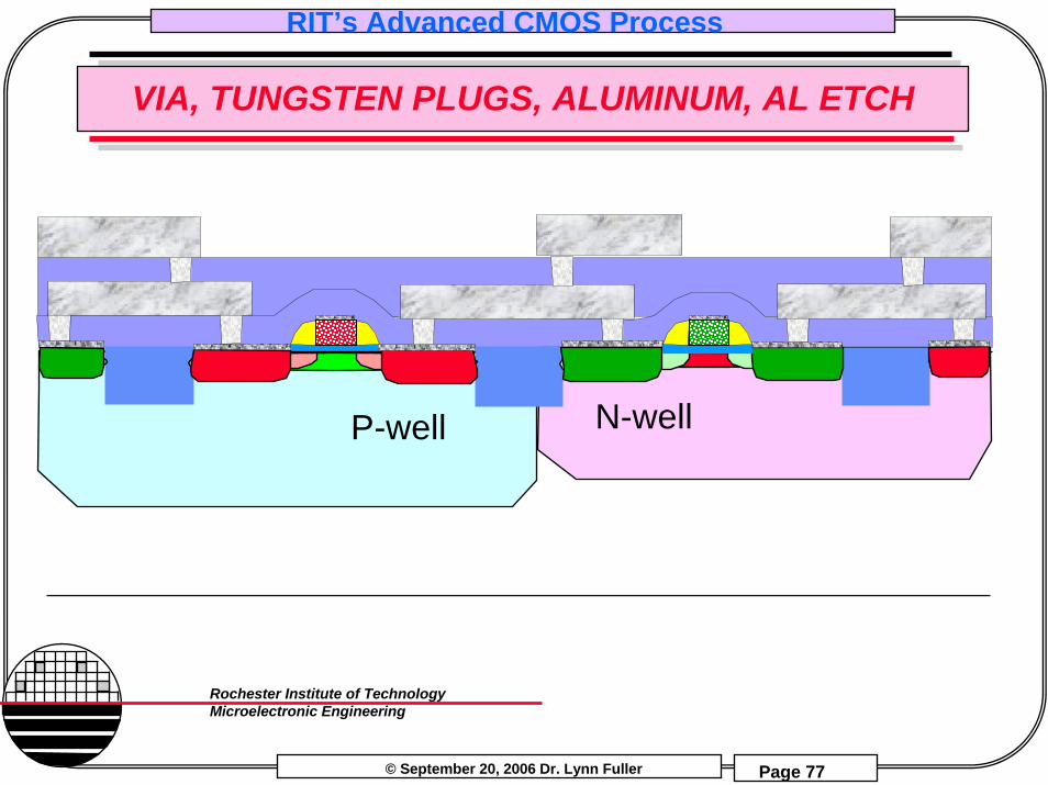
VIA, TUNGSTEN PLUGS, ALUMINUM, AL ETCH
P-well N-well
© September 20, 2006 Dr. Lynn Fuller
RIT’s Advanced CMOS Process
Page 78
Rochester Institute of TechnologyMicroelectronic Engineering
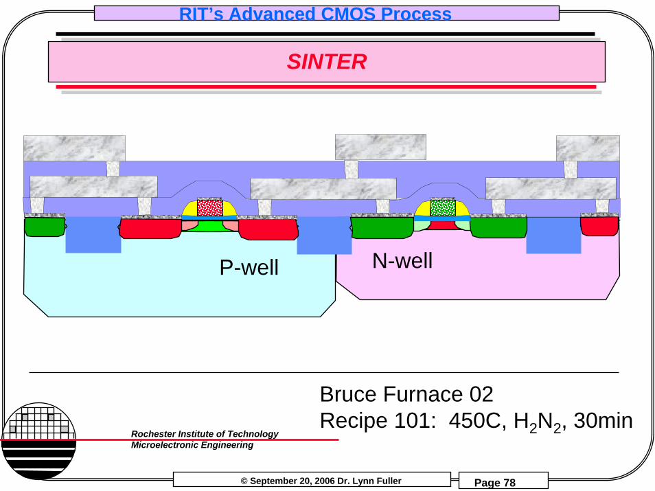
SINTER
Bruce Furnace 02 Recipe 101: 450C, H2N2, 30min
P-well N-well
© September 20, 2006 Dr. Lynn Fuller
RIT’s Advanced CMOS Process
Page 79
Rochester Institute of TechnologyMicroelectronic Engineering
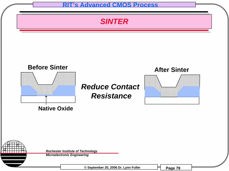
SINTER
Native Oxide
Before Sinter After Sinter
Reduce Contact Resistance
© September 20, 2006 Dr. Lynn Fuller
RIT’s Advanced CMOS Process
Page 80
Rochester Institute of TechnologyMicroelectronic Engineering
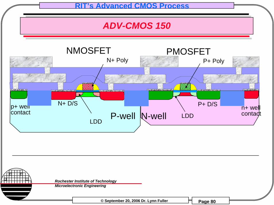
ADV-CMOS 150
NMOSFET PMOSFET
N-wellP-well
N+ Poly
P+ D/SN+ D/S
LDDLDD
n+ wellcontact
p+ wellcontact
P+ Poly
© September 20, 2006 Dr. Lynn Fuller
RIT’s Advanced CMOS Process
Page 81
Rochester Institute of TechnologyMicroelectronic Engineering
REFERENCES
1. Silicon Processing for the VLSI Era, Volume 1 – Process Technology, 2nd, S. Wolf and R.N. Tauber, Lattice Press.
2. The Science and Engineering of Microelectronic Fabrication, Stephen A. Campbell, Oxford University Press, 1996.
© September 20, 2006 Dr. Lynn Fuller
RIT’s Advanced CMOS Process
Page 82
Rochester Institute of TechnologyMicroelectronic Engineering
SUMMARY
Thanks again to Dr. Lynn Fuller for providing this material. Please visit the RI website for more information.
http://www.rit.edu/~lffeee/ Microelectronic EngineeringRochester Institute of Technology82 Lomb Memorial DriveRochester, NY 14623-5604Tel (585) 475-2035Fax (585) 475-5041
email: [email protected]
microE webpage: http://www.microe.rit.edu