Embed Size (px)
Citation preview
© January 20, 2015, Dr. Lynn Fuller, Professor
Rochester Institute of TechnologyMicroelectronic Engineering
CMOS Factory
Page 1
ROCHESTER INSTITUTE OF TECHNOLOGYMICROELECTRONIC ENGINEERING
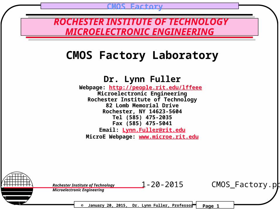
CMOS Factory Laboratory
Dr. Lynn Fuller Webpage: http://people.rit.edu/lffeee
Microelectronic Engineering Rochester Institute of Technology
82 Lomb Memorial Drive Rochester, NY 14623-5604
Tel (585) 475-2035 Fax (585) 475-5041
Email: [email protected] MicroE Webpage: www.microe.rit.edu
1-20-2015 CMOS_Factory.ppt
© January 20, 2015, Dr. Lynn Fuller, Professor
Rochester Institute of TechnologyMicroelectronic Engineering
CMOS Factory
Page 2
INTRODUCTION
This document contains items that should be included in the students lab notebook. This includes general information about the processes and products made in the student factory.
© January 20, 2015, Dr. Lynn Fuller, Professor
Rochester Institute of TechnologyMicroelectronic Engineering
CMOS Factory
Page 3
INTRODUCTION
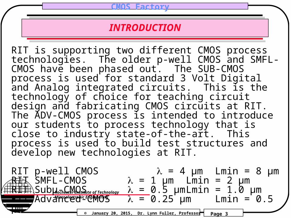
RIT is supporting two different CMOS process technologies. The older p-well CMOS and SMFL-CMOS have been phased out. The SUB-CMOS process is used for standard 3 Volt Digital and Analog integrated circuits. This is the technology of choice for teaching circuit design and fabricating CMOS circuits at RIT. The ADV-CMOS process is intended to introduce our students to process technology that is close to industry state-of-the-art. This process is used to build test structures and develop new technologies at RIT.
RIT p-well CMOS = 4 µm Lmin = 8 µmRIT SMFL-CMOS = 1 µm Lmin = 2 µmRIT Subµ-CMOS = 0.5 µm Lmin = 1.0 µmRIT Advanced-CMOS = 0.25 µm Lmin = 0.5 µm
© January 20, 2015, Dr. Lynn Fuller, Professor
Rochester Institute of TechnologyMicroelectronic Engineering
CMOS Factory
Page 4
RIT SUBµ CMOS
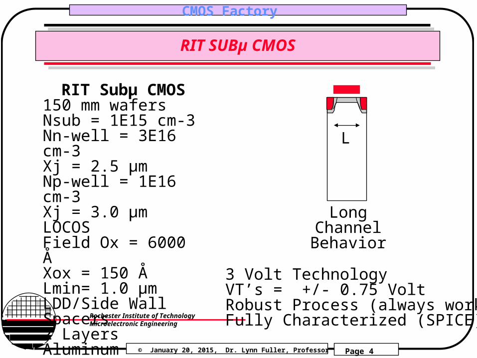
RIT Subµ CMOS150 mm wafersNsub = 1E15 cm-3Nn-well = 3E16 cm-3Xj = 2.5 µmNp-well = 1E16 cm-3Xj = 3.0 µmLOCOSField Ox = 6000 Å Xox = 150 ÅLmin= 1.0 µmLDD/Side Wall Spacers2 Layers Aluminum
L
LongChannelBehavior
3 Volt TechnologyVT’s = +/- 0.75 VoltRobust Process (always works)Fully Characterized (SPICE)
© January 20, 2015, Dr. Lynn Fuller, Professor
Rochester Institute of TechnologyMicroelectronic Engineering
CMOS Factory
Page 5
RIT SUBµ CMOS
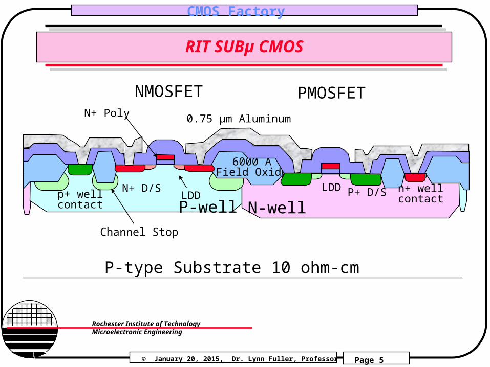
0.75 µm Aluminum
P-type Substrate 10 ohm-cm
P-well N-well
6000 ÅField Oxide
NMOSFET PMOSFETN+ Poly
Channel Stop
P+ D/SN+ D/SLDD
LDD n+ wellcontactp+ well
contact
© January 20, 2015, Dr. Lynn Fuller, Professor
Rochester Institute of TechnologyMicroelectronic Engineering
CMOS Factory
Page 6
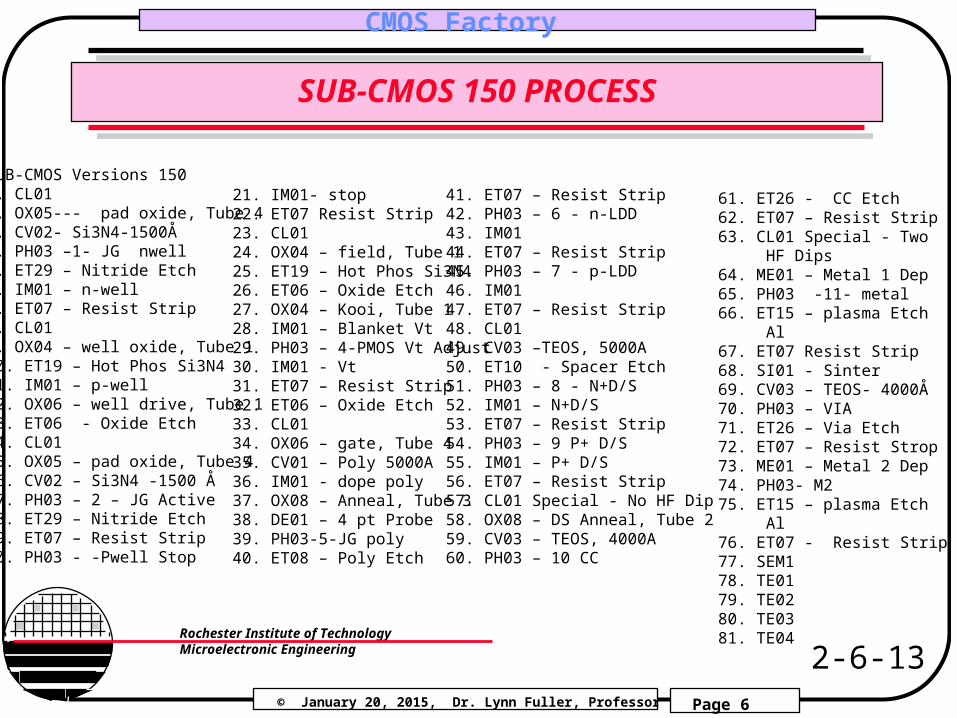
SUB-CMOS 150 PROCESS
SUB-CMOS Versions 1501. CL012. OX05--- pad oxide, Tube 43. CV02- Si3N4-1500Å4. PH03 –1- JG nwell5. ET29 – Nitride Etch6. IM01 – n-well7. ET07 – Resist Strip8. CL019. OX04 – well oxide, Tube 110. ET19 – Hot Phos Si3N411. IM01 – p-well12. OX06 – well drive, Tube 113. ET06 - Oxide Etch14. CL0115. OX05 – pad oxide, Tube 416. CV02 – Si3N4 -1500 Å17. PH03 – 2 – JG Active18. ET29 – Nitride Etch19. ET07 – Resist Strip20. PH03 - -Pwell Stop
61. ET26 - CC Etch62. ET07 – Resist Strip63. CL01 Special - Two HF Dips64. ME01 – Metal 1 Dep65. PH03 -11- metal66. ET15 – plasma Etch Al67. ET07 Resist Strip68. SI01 - Sinter69. CV03 – TEOS- 4000Å70. PH03 – VIA71. ET26 – Via Etch72. ET07 – Resist Strop73. ME01 – Metal 2 Dep74. PH03- M275. ET15 – plasma Etch Al76. ET07 - Resist Strip77. SEM178. TE0179. TE0280. TE0381. TE04
21. IM01- stop22. ET07 Resist Strip23. CL0124. OX04 – field, Tube 125. ET19 – Hot Phos Si3N426. ET06 – Oxide Etch27. OX04 – Kooi, Tube 128. IM01 – Blanket Vt29. PH03 – 4-PMOS Vt Adjust30. IM01 - Vt31. ET07 – Resist Strip32. ET06 – Oxide Etch33. CL0134. OX06 – gate, Tube 435. CV01 – Poly 5000A36. IM01 - dope poly37. OX08 – Anneal, Tube 338. DE01 – 4 pt Probe39. PH03-5-JG poly40. ET08 – Poly Etch
41. ET07 – Resist Strip42. PH03 – 6 - n-LDD43. IM0144. ET07 – Resist Strip45. PH03 – 7 - p-LDD46. IM0147. ET07 – Resist Strip48. CL0149. CV03 –TEOS, 5000A50. ET10 - Spacer Etch51. PH03 – 8 - N+D/S52. IM01 – N+D/S53. ET07 – Resist Strip54. PH03 – 9 P+ D/S55. IM01 – P+ D/S56. ET07 – Resist Strip57. CL01 Special - No HF Dip58. OX08 – DS Anneal, Tube 259. CV03 – TEOS, 4000A60. PH03 – 10 CC
2-6-13
© January 20, 2015, Dr. Lynn Fuller, Professor
Rochester Institute of TechnologyMicroelectronic Engineering
CMOS Factory
Page 7
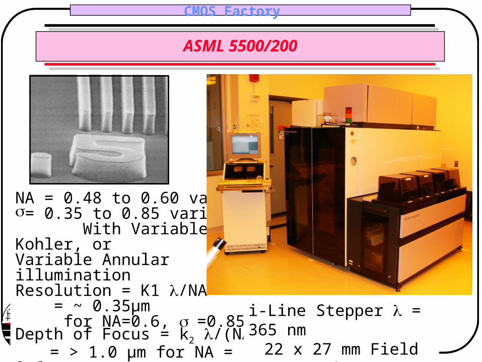
ASML 5500/200
NA = 0.48 to 0.60 variable= 0.35 to 0.85 variable With Variable Kohler, orVariable Annular illuminationResolution = K1 /NA = ~ 0.35µm
for NA=0.6, =0.85 Depth of Focus = k2 /(NA)2
= > 1.0 µm for NA = 0.6i-Line Stepper = 365 nm
22 x 27 mm Field Size

RIT SUB-CMOS PROCESS
11 PHOTOLEVELS
POLY
METAL
N-WELL
P SELECTCC
ACTIVE
0.75 µm Aluminum
P-type Substrate 10 ohm-cm
P-well N-well
6000 ÅField Oxide
NMOSFET PMOSFETN+ Poly
Channel Stop
P+ D/SN+ D/S LDDLDD n+ well
contactp+ wellcontact
LVL 1 – n-WELL
LVL 11 - METAL
LVL 4 - PMOS VT
LVL 9 - N+ D/S
LVL 2 - ACTIVE
LVL 8 - P+ D/S
LVL 3 - STOP
LVL 10 - CC
LVL 5 - POLY
LVL 7 – N-LDD
LVL 6 – P-LDD
N SELECT
© January 20, 2015, Dr. Lynn Fuller, Professor
Rochester Institute of TechnologyMicroelectronic Engineering
CMOS Factory
Page 9
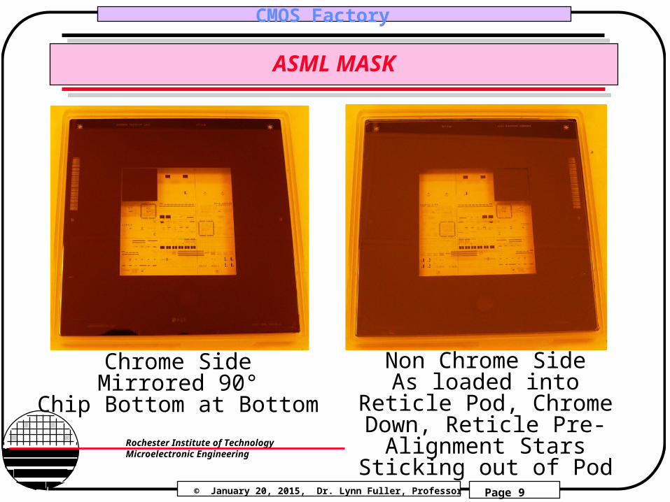
ASML MASK
Chrome SideMirrored 90°
Chip Bottom at Bottom
Non Chrome SideAs loaded into Reticle Pod, Chrome Down, Reticle Pre- Alignment Stars Sticking out
of Pod
© January 20, 2015, Dr. Lynn Fuller, Professor
Rochester Institute of TechnologyMicroelectronic Engineering
CMOS Factory
Page 10
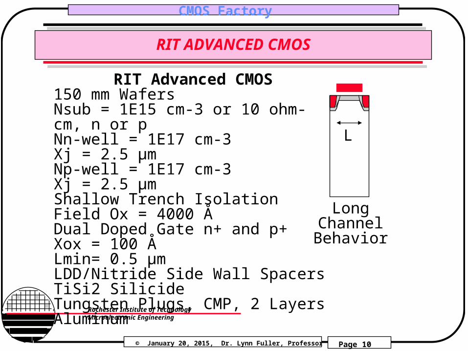
RIT ADVANCED CMOS
RIT Advanced CMOS150 mm WafersNsub = 1E15 cm-3 or 10 ohm-cm, n or pNn-well = 1E17 cm-3Xj = 2.5 µmNp-well = 1E17 cm-3Xj = 2.5 µmShallow Trench IsolationField Ox = 4000 Å Dual Doped Gate n+ and p+Xox = 100 ÅLmin= 0.5 µmLDD/Nitride Side Wall SpacersTiSi2 SilicideTungsten Plugs, CMP, 2 Layers Aluminum
L
LongChannelBehavior

© January 20, 2015, Dr. Lynn Fuller, Professor
Rochester Institute of TechnologyMicroelectronic Engineering
CMOS Factory
Page 11
RIT ADVANCED CMOS
NMOSFET PMOSFET
N-wellP-well
N+ Poly
P+ D/SN+ D/S
LDDLDD
n+ wellcontact
p+ wellcontact
P+ Poly

© January 20, 2015, Dr. Lynn Fuller, Professor
Rochester Institute of TechnologyMicroelectronic Engineering
CMOS Factory
Page 12
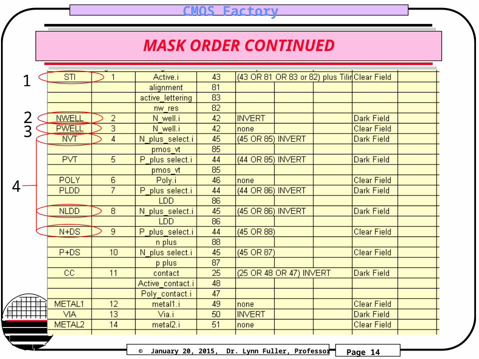
ADV-CMOS 150 PROCESS
ADV-CMOS Versions 150, Two level Metal1. OX05--- pad oxide 500 Å, Tube 42. CV02- 1500 Å Si3N4 Deposition3. PH03 – level 1- STI4. ET29 - etch Nitride 5. ET07 – ash 6. CL01 – RCA clean7. OX04 – First Oxide Tube 18. ET06 – Etch Oxide9. OX04 – 2nd Oxide Tube 110. ET19 – Etch Nitride11. PH03 – level 2 - N-well12. IM01 – 5E13, P31, 170 KeV13. ET07 – ash 14. PH03 – level 3 - P-well15. IM01 – 7E13, B11, 100 KeV16. ET07 – ash 17. OX06 – Well Drive, Tube 118. PH03 – level 4 - N-well retrograde19. IM01 – 9E13, P31, 70 KeV20. ET07 - ash
21. PH03 – level 5 - P-well retrograde22. IM01 – 1E14, B11, 45 KeV23. ET07 – ash 24. ET06 – etch 500 Å pad oxide25. CL01 – pre-gate oxide RCA clean26. ET06 – etch native oxide 27. OX06 – 30 Å gate oxide, Tube 428. CV01 – poly deposition, 2500 Å29. PH03 – level 6 - poly gate30. ET08 – poly gate plasma etch31. ET07 – ash 32. CL01 – RCA clean33. OX05 – poly re-ox, 250 Å, Tube 434. PH03 – level 7 - p-LDD35. IM01 – 9E14, BF2, 20 KeV 36. ET07 – ash 37. PH03 – level 8 - n-LDD38. IM01 – 5E15, P31, 20 KeV39. ET07 – ash 40. CL01 – RCA clean
41. CV02 – nitride spacer 2500Å42. ET39 – sidewall spacer etch43. PH03 – level 9 - N+D/S44. IM01 – 1E15, P31, 25 KeV45. ET07 – ash 46. PH03 – level 10 - P+ D/S47. IM01 – 5E15 BF2, 27 KeV48. ET07 – ash 49. CL01 – RCA clean50. OX08 – DS Anneal, RTP51. ET06 – Silicide pad ox etch52. ME03 – HF dip & Ti Sputter53. RT01 – RTP 5 sec, 650C54. ET11 – Unreacted Ti Etch55. RT02 – RTP 5 sec, 700C56. CV03 – TEOS, P-5000, 3000Å57. PH03 – level 11 - CC58. ET06 – CC etch59. ET07 – ash 60. CL01 – RCA clean
61. ME01 – Aluminum 62. PH03 – level 12-metal63. ET15 – plasma Al Etch64. ET07 – ash 65. CV03 – TEOS66. PH03 – Via67. ET26 Via Etch68. ME01 Al Deposition69. PH03 – Metal 270. ET07 - Ash72. SI01 – sinter 73. SEM174. TE0175. TE0276. TE0377. TE04
(Revision 05-02-14)L = 0.5 mVDD = 3.0 VVTN = 0.75 VVTP = - 0.75V
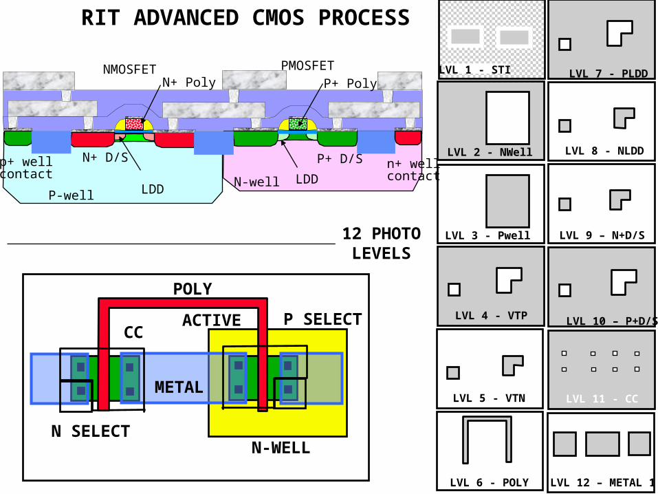
RIT ADVANCED CMOS PROCESS
POLY
METAL
N-WELL
P SELECTCC
ACTIVE
N SELECT
LVL 2 - NWell
LVL 3 - Pwell
LVL 6 - POLY
LVL 8 - NLDD
LVL 11 - CC
LVL 12 – METAL 1
LVL 9 – N+D/S
LVL 10 – P+D/S
LVL 7 - PLDD
LVL 4 - VTP
NMOSFET PMOSFET
N-wellP-well
N+ Poly
P+ D/SN+ D/S
LDDLDD
n+ wellcontact
p+ wellcontact
P+ PolyLVL 1 - STI
12 PHOTOLEVELS
LVL 5 - VTN
© January 20, 2015, Dr. Lynn Fuller, Professor
Rochester Institute of TechnologyMicroelectronic Engineering
CMOS Factory
Page 14
MASK ORDER CONTINUED
1
32
4
© January 20, 2015, Dr. Lynn Fuller, Professor
Rochester Institute of TechnologyMicroelectronic Engineering
CMOS Factory
Page 15
PRODUCTS
New John Galt Test Chip (Sub-CMOS and Adv-CMOS)
Older Obsolete Chips:Mixed Analog/Digital Test Chip (Sub-CMOS Process)Test Chip (Advanced CMOS Process) John Galt Test Chip (Sub-CMOS Process)4-Bit Microprocessor (Sub-CMOS Process)Analog to Digital Converter (Sub-CMOS Process)
© January 20, 2015, Dr. Lynn Fuller, Professor
Rochester Institute of TechnologyMicroelectronic Engineering
CMOS Factory
Page 16
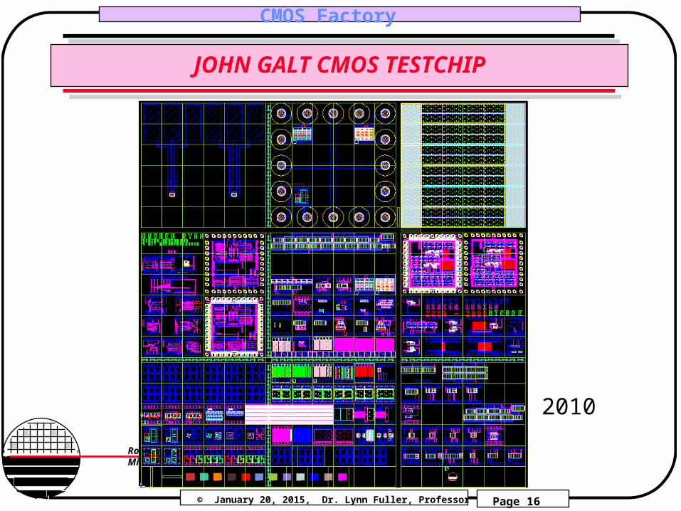
JOHN GALT CMOS TESTCHIP
2010
© January 20, 2015, Dr. Lynn Fuller, Professor
Rochester Institute of TechnologyMicroelectronic Engineering
CMOS Factory
Page 17
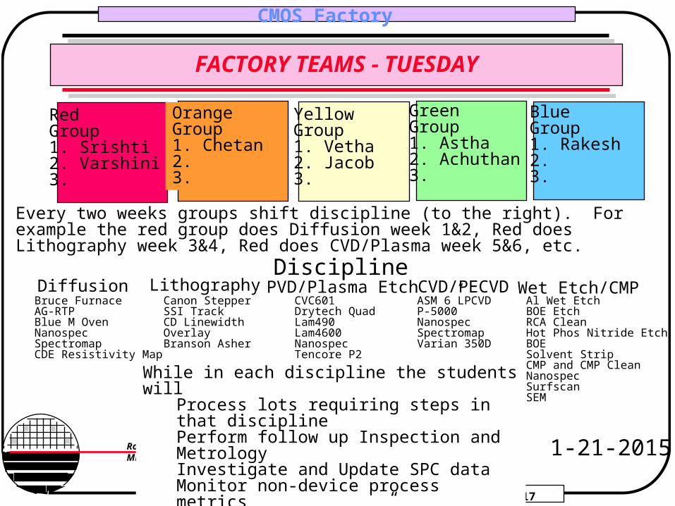
FACTORY TEAMS - TUESDAY
OrangeGroup1. Chetan2. 3.
YellowGroup1. Vetha2. Jacob3.
BlueGroup1. Rakesh2. 3.
GreenGroup1. Astha2. Achuthan3.
Diffusion PVD/Plasma Etch CVD/PECVDLithography Wet Etch/CMPAl Wet EtchBOE EtchRCA CleanHot Phos Nitride EtchBOESolvent StripCMP and CMP CleanNanospecSurfscanSEM
CVC601Drytech QuadLam490Lam4600NanospecTencore P2
Canon StepperSSI TrackCD LinewidthOverlayBranson Asher
Bruce FurnaceAG-RTPBlue M OvenNanospecSpectromapCDE Resistivity Map
ASM 6”LPCVDP-5000NanospecSpectromapVarian 350D
While in each discipline the students willProcess lots requiring steps in that disciplinePerform follow up Inspection and MetrologyInvestigate and Update SPC dataMonitor non-device process metricsPerform a “pass down” at the end of (2 weeks)Track lots in and out of Mesa
Discipline
RedGroup1. Srishti2. Varshini3.
Every two weeks groups shift discipline (to the right). For example the red group does Diffusion week 1&2, Red does Lithography week 3&4, Red does CVD/Plasma week 5&6, etc.
1-21-2015
© January 20, 2015, Dr. Lynn Fuller, Professor
Rochester Institute of TechnologyMicroelectronic Engineering
CMOS Factory
Page 18
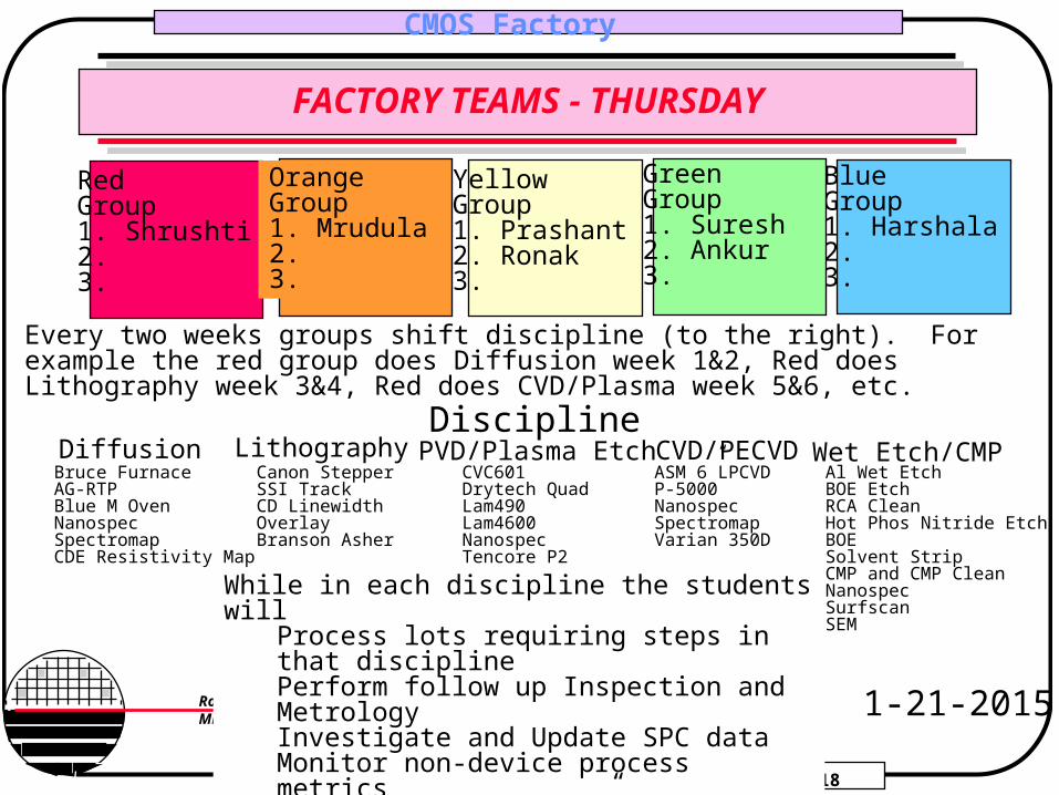
FACTORY TEAMS - THURSDAY
OrangeGroup1. Mrudula2. 3.
BlueGroup1. Harshala2. 3.
GreenGroup1. Suresh2. Ankur3.
Diffusion PVD/Plasma Etch CVD/PECVDLithography Wet Etch/CMPAl Wet EtchBOE EtchRCA CleanHot Phos Nitride EtchBOESolvent StripCMP and CMP CleanNanospecSurfscanSEM
CVC601Drytech QuadLam490Lam4600NanospecTencore P2
Canon StepperSSI TrackCD LinewidthOverlayBranson Asher
Bruce FurnaceAG-RTPBlue M OvenNanospecSpectromapCDE Resistivity Map
ASM 6”LPCVDP-5000NanospecSpectromapVarian 350D
While in each discipline the students willProcess lots requiring steps in that disciplinePerform follow up Inspection and MetrologyInvestigate and Update SPC dataMonitor non-device process metricsPerform a “pass down” at the end of (2 weeks)Track lots in and out of Mesa
Discipline
RedGroup1. Shrushti2. 3.
Every two weeks groups shift discipline (to the right). For example the red group does Diffusion week 1&2, Red does Lithography week 3&4, Red does CVD/Plasma week 5&6, etc.
1-21-2015
YellowGroup1. Prashant2. Ronak3.

© January 20, 2015, Dr. Lynn Fuller, Professor
Rochester Institute of TechnologyMicroelectronic Engineering
CMOS Factory
Page 19
EXAMPLE TEAM REPORT AT END OF ROTATION
Discipline: Lithography Date: Nov 30- Dec 8, 2014Group Members: Matt McQuillan, Dave Pawlik
Lot Advancement: F031013 – CC Photo –Changed Stepper Job to Align using TVPA Marks Only
added 2 µm shift to alignment key locations on pg 4/ in process fileF040119 – Resist StripF040614 – Active PhotoF031013 – LDDP PhotoF040920 – Resist Strip-Changed Stepper Job to Align using TVPA Marks OnlyF040920 – P-Well Photo-Changed Stepper Job to Align using TVPA Marks OnlyF030922- Resist Strip
Other: Short Loop Resist Coat Thickness measurement for Coat.rcp, Xpr=1.0 µmBranson Asher often gives purge timeout error, select continue
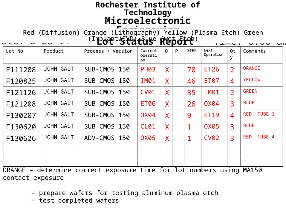
Lot No Product Process / Version Current operation
Q P STEP Next Operation
Qty Comments
F111208 JOHN GALT SUB-CMOS 150 PH03 X 70 ET26 2 ORANGE
F120825 JOHN GALT SUB-CMOS 150 IM01 X 46 ET07 4 YELLOW
F121126 JOHN GALT SUB-CMOS 150 CV01 X 35 IM01 2 GREEN
F121208 JOHN GALT SUB-CMOS 150 ET06 X 26 OX04 3 BLUE
F130207 JOHN GALT SUB-CMOS 150 OX04 X 9 ET19 4 RED, TUBE 1
F130620 JOHN GALT SUB-CMOS 150 CL01 X 1 OX05 3 BLUE
F130626 JOHN GALT ADV-CMOS 150 OX05 X 1 CV02 3 RED, TUBE 4
Rochester Institute of TechnologyMicroelectronic Engineering
Dr. Lynn Fuller
Date: 8-26-14 Time: 8:00 amRed (Diffusion) Orange (Lithography) Yellow (Plasma Etch) Green (Implant/CVD) Blue (wet Etch)
ORANGE – determine correct exposure time for lot numbers using MA150 contact exposure
- prepare wafers for testing aluminum plasma etch- test completed wafers
Lot Status Report
© January 20, 2015, Dr. Lynn Fuller, Professor
Rochester Institute of TechnologyMicroelectronic Engineering
CMOS Factory
Page 21
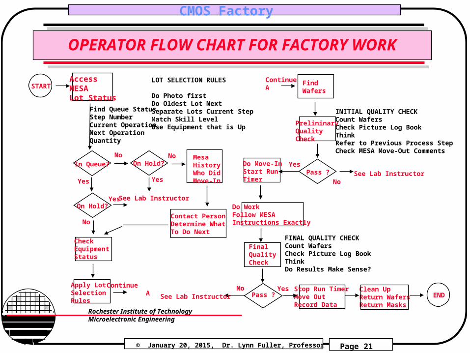
OPERATOR FLOW CHART FOR FACTORY WORK
LOT SELECTION RULES
Do Photo firstDo Oldest Lot NextSeparate Lots Current StepMatch Skill LevelUse Equipment that is Up
Apply LotSelection Rules
Check EquipmentStatus
In Queue?
AccessMESALot Status
On Hold?
On Hold?
PrelininaryQualityCheck
Find Wafers
Do WorkFollow MESAInstructions Exactly
Do Move-InStart RunTimer
Pass ?
FINAL QUALITY CHECKCount WafersCheck Picture Log BookThinkDo Results Make Sense?
Contact PersonDetermine WhatTo Do Next
FinalQualityCheck
Yes
YesSee Lab Instructor
Yes
No
No
No
No
INITIAL QUALITY CHECKCount WafersCheck Picture Log BookThinkRefer to Previous Process StepCheck MESA Move-Out Comments
START
Mesa HistoryWho DidMove-In
Find Queue StatusStep NumberCurrent OperationNext Operation Quantity
See Lab Instructor
Pass ?Clean UpReturn WafersReturn Masks
Stop Run TimerMove OutRecord Data
ENDNo
See Lab InstructorYes
ContinueA
Continue A
Yes

© January 20, 2015, Dr. Lynn Fuller, Professor
Rochester Institute of TechnologyMicroelectronic Engineering
CMOS Factory
Page 22
SPC CHARTS
SPC6SC_FO Field Oxide ThicknessSPC6SC_GOX Gate Oxide ThicknessSPC6SC_KOX Kooi Oxide ThicknessSPC6SC_LTO LTO/TEOX Oxide ThicknessSPC6SC_MTL Metal ThicknessSPC6SC_N1 Nitride Thickness (1500Å)SPC6SC_N2 Nitride Thickness (3500Å)SPC6SC_PADPad Oxide ThicknessSPC6SC_POL Poly ThicknessSPC6SC_WO Well Oxide ThicknessSPC6SCPROSPoly Sheet Resistance
© January 20, 2015, Dr. Lynn Fuller, Professor
Rochester Institute of TechnologyMicroelectronic Engineering
CMOS Factory
Page 23
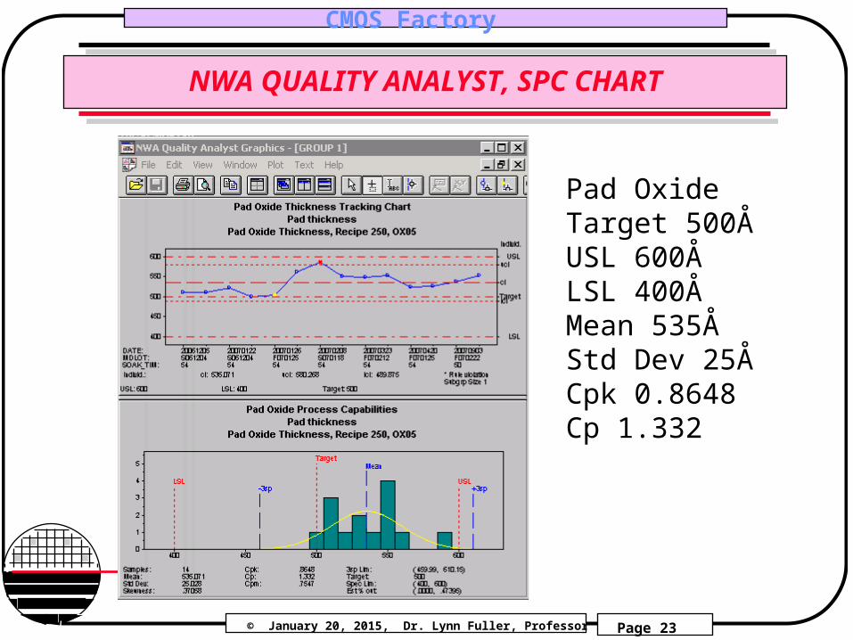
NWA QUALITY ANALYST, SPC CHART
Pad OxideTarget 500ÅUSL 600ÅLSL 400ÅMean 535ÅStd Dev 25ÅCpk 0.8648Cp 1.332
© January 20, 2015, Dr. Lynn Fuller, Professor
Rochester Institute of TechnologyMicroelectronic Engineering
CMOS Factory
Page 24
MANUFACTURING IMPROVEMENT
If no factory lots are available in a specific discipline then group will do manufacturing improvement projects.
For Example:BOE – Etch rate verificationRTP – Tool operation and recipe verificationPECVD – Tool operation and deposition rate verification,TEOS OxideResist Coat Thickness Measurement using Spectromap for Coat.rcp and
CoatMtl.rcp Recipes used by FactorySPC Chart verification, evaluation and process capability improvementVerify all MESA picture documents are correctVerify MESA instructions are correct