Embed Size (px)
Citation preview

Roadmap on all-optical processing
Downloaded from: https://research.chalmers.se, 2021-11-18 03:53 UTC
Citation for the original published paper (version of record):Minzioni, P., Lacava, C., Tanabe, T. et al (2019)Roadmap on all-optical processingJournal of Optics, 21(6)http://dx.doi.org/10.1088/2040-8986/ab0e66
N.B. When citing this work, cite the original published paper.
research.chalmers.se offers the possibility of retrieving research publications produced at Chalmers University of Technology.It covers all kind of research output: articles, dissertations, conference papers, reports etc. since 2004.research.chalmers.se is administrated and maintained by Chalmers Library
(article starts on next page)

Journal of Optics
ROADMAP • OPEN ACCESS
Roadmap on all-optical processingTo cite this article: Paolo Minzioni et al 2019 J. Opt. 21 063001
View the article online for updates and enhancements.
Recent citationsEngineering optical hybrid entanglementbetween discrete- and continuous-variablestatesKun Huang et al
-
This content was downloaded from IP address 129.16.86.92 on 27/08/2019 at 09:39

Roadmap
Roadmap on all-optical processing
Paolo Minzioni1,27 , Cosimo Lacava2,27 , Takasumi Tanabe3, Jianji Dong4,Xiaoyong Hu5 , Gyorgy Csaba6, Wolfgang Porod7, Ghanshyam Singh8,Alan E Willner9, Ahmed Almaiman9,10 , Victor Torres-Company11,Jochen Schröder11, Anna C Peacock2 , Michael J Strain12,Francesca Parmigiani2, Giampiero Contestabile13, David Marpaung14,Zhixin Liu15, John E Bowers16 , Lin Chang16, Simon Fabbri17,María Ramos Vázquez18, Vibhav Bharadwaj19 , Shane M Eaton19,Peter Lodahl20, Xiang Zhang21, Benjamin J Eggleton21 ,William John Munro22, Kae Nemoto23, Olivier Morin24, Julien Laurat25 andJoshua Nunn26
1Università di Pavia, Via Ferrata, 5A, 27100 Pavia, Italy2Optoelectronics Research Centre, Zepler Institute, University of Southampton, Southampton, UnitedKingdom3Keio University, Japan4Huazhong University of Science and Technology, People’s Republic of China5 Peking University, People’s Republic of China6 Pazmany University, Budapest, Hungary7University of Notre Dame, IN, United States of America8Department of Electronics and Communication Engineering, Malaviya National Institute of TechnologyJaipur, 302017 India9University of Southern California, CA, United States of America10King Saud University, Saudi Arabia11Department of Microtechnology and Nanoscience, Chalmers University of Technology, SE 41296Gothenburg, Sweden12University of Strathclyde, Glasgow, United Kingdom13 Scuola Superiore Sant’Anna, Pisa, Italy14University of Twente, The Netherlands15University College London, London, United Kingdom16Department of Electrical and Computer Engineering, University of California, Santa Barbara, CA 93106,United States of America17 École Polytechnique Fédérale de Lausanne, Switzerland18 Centre for Disruptive Photonic Technologies, Nanyang Technological University, Singapore19 Instituto di Fotonica e Nanotecnologie-Consiglio Nazionale delle Ricerche (IFN-CNR), Milano, Italy20 Center for Hybrid Quantum Networks (Hy-Q), Niels Bohr Institute, University of Copenhagen,Blegdamsvej 17, DK-2100 Copenhagen, Denmark21University of Sydney, Sydney, Australia22NTT Basic Research Laboratories, Japan23National Institute of Informatics, Japan24Max-Planck-Institut für Quantenoptik, Hans-Kopfermann-Strasse 1, 85748 Garching, Germany25 Laboratoire Kastler Brossel, Sorbonne Université, CNRS, ENS-PSL Université, Collège de France, 4place Jussieu, 75005 Paris, France26University of Bath, Bath, United Kingdom
E-mail: [email protected] and [email protected]
Journal of Optics
J. Opt. 21 (2019) 063001 (55pp) https://doi.org/10.1088/2040-8986/ab0e66
27 Guest editors of the Roadmap
2040-8978/19/063001+55$33.00 © 2019 IOP Publishing Ltd Printed in the UK1

Received 15 June 2018, revised 18 December 2018Accepted for publication 8 March 2019Published 17 May 2019
AbstractThe ability to process optical signals without passing into the electrical domain has always attractedthe attention of the research community. Processing photons by photons unfolds new scenarios, inprinciple allowing for unseen signal processing and computing capabilities. Optical computation canbe seen as a large scientific field in which researchers operate, trying to find solutions to their specificneeds by different approaches; although the challenges can be substantially different, they are typicallyaddressed using knowledge and technological platforms that are shared across the whole field. Thissignificant know-how can also benefit other scientific communities, providing lateral solutions to theirproblems, as well as leading to novel applications. The aim of this Roadmap is to provide a broadview of the state-of-the-art in this lively scientific research field and to discuss the advances required totackle emerging challenges, thanks to contributions authored by experts affiliated to both academicinstitutions and high-tech industries. The Roadmap is organized so as to put side by side contributionson different aspects of optical processing, aiming to enhance the cross-contamination of ideas betweenscientists working in three different fields of photonics: optical gates and logical units, high bit-ratesignal processing and optical quantum computing. The ultimate intent of this paper is to provideguidance for young scientists as well as providing research-funding institutions and stake holders witha comprehensive overview of perspectives and opportunities offered by this research field.
Keywords: optical computing, all-optical processing, quantum computing, optical gates, opticalsignal processing
(Some figures may appear in colour only in the online journal)
Contents
1. Introduction 4
LOGIC UNITS AND GATES 6
2. Cavity-based all optical flip-flops and logic gates 6
3. All optical gates based on semiconductor optical amplifiers 8
4. Nanoscale all-optical logics 10
5. Non-Boolean optically-inspired computing using spin waves 12
SIGNAL PROCESSING FOR TELECOM APPLICATIONS 14
6. Optical resonant structures for signal manipulation 14
7. Optical regeneration 16
8. Kerr nonlinear waveguides for telecom-oriented all-optical signal processing 18
9. Nonlinear all-optical processing in silicon core fibres 20
10. Novel silicon photonic devices and processes 22
11. Multi-mode based all-optical nonlinear signal processors 24
12. Optical signal processing using semiconductor optical amplifiers (SOAs) 26
13. Integrated microwave photonic signal processing 28
14. Analogue signal processing for data centre interconnections 30
15. Heterogeneous integration for optical signal processing 32
16. All-optical multiplexing & demultiplexing 35
Original content from this work may be used under the termsof the Creative Commons Attribution 3.0 licence. Any
further distribution of this work must maintain attribution to the author(s) andthe title of the work, journal citation and DOI.
2
J. Opt. 21 (2019) 063001 Roadmap

QUANTUM PROCESSING 37
17. Diamond quantum computing 37
18. Quantum-information processing with single photons generated by quantum dots 39
19. Chip-based photon quantum state sources using nonlinear optics 41
20. Weak optical nonlinearities and their potential for efficient universal quantum computation 43
21. Generation and amplification of optical Schrödinger cats 45
22. Linear optical quantum computing 47
List of Acronyms
3PA Three photon absorption
ADC Analogue-to-digital converter
AlGaAs Aluminum gallium arsenide
AO-OFDM All-optical orthogonal frequency divisionmultiplexing
ASE Amplified spontaneous emission
a-Si:H Hydrogenated amorphous silicon
CD Chromatic dispersion
CDR Clock and data recovery
CMOS Complementary metal-oxide semiconductor
CNOT Controlled NOT
CVD Chemical vapor deposition
CW Continuous wave
DAC Digital-to-analog converter
DC Data centre
DCN Data centre network
DPSK Differential phase-shift keying
DSP Digital signal processing
EDFA Erbium-doped fiber amplifier
EVM Error vector magnitude
FEC Forward error code
FFT Fast Fourier transform
FWM Four-wave mixing
GaAs Gallium arsenide
HOMs Higher order modes
I/O Input/output
ICT Information and communications technology
InGaAs Indium gallium arsenide
InP Indium phosphide
KLM Knill Laflamme and Milburn
MMFs Multi-mode fibres
MWP Microwave photonics
MZ Mach-Zehnder
MZI Mach-Zehnder interferometer
NF Noise figure
NRZ Non return to zero
OEO Optical/electrical/optical
OFDM Orthogonal frequency division multiplexing
OOK On-Off keying
OSNR Optical signal-to-noise ratio
OTDM Orthogonal time division multiplexing
PAM Pulse amplitude modulation
PDL Polarization dependent loss
PIC Photonic integrated circuit
PLA Programmable logic array
PMD Polarization mode dispersion
PSA Phase-sensitive amplifier
PSK Phase-shift keying
QAM Quadrature amplitude modulation
QD Quantum dot
QIP Quantum information processing
QND Quantum non-demolition
QPSK Quadrature phase-shift keying
RF Radio frequency
ROADM Reconfigurable optical add/drop multiplexer
RZ Return to zero
SDM Space-division multiplexing
SFDR Spurious-free dynamic range
SNR Signal-to-noise ratio
SOA Semiconductor optical amplifier
SOI Silicon-on-insulator
SoP State of polarization
SPM Self-phase modulation
SPP Surface plasmon polariton
TE Transverse electric
TIDE Terabit interferometric add, drop, and extract
TM Transverse magnetic
TPA Two-photon absorption
WDM Wavelength division multiplexing
WGM Whispering gallery mode
WSS Wavelength selective switch
XAM Cross-absorption modulation
XGM Cross-gain modulation
XPM Cross-phase modulation
XPolM Cross-polarization modulation
3
J. Opt. 21 (2019) 063001 Roadmap
1. Introduction
Paolo Minzioni1and Cosimo Lacava2
1University of Pavia, Pavia, Italy2Optoelectronics Research Centre, Zepler Insitute, University ofSouthampton, Southampton, United Kingdom
The importance of all-optical processing. The advent of thecurrent era (often regarded as the ‘information age’) has beenenabled by the capability of transferring and processing largequantity of information in a relatively small amount of time.Specifically, while data are generally encoded on photons fortransmission, the information is then converted to theelectronic domain for the processing phase. This is relatedto a fundamental difference between electrons and photons:electrons can strongly interact with each other even invacuum, while photon–photon interactions require thepresence of a suitable medium to enable such aninteraction. For this reason, electronic systems are generallyused to perform signal processing and nonlinear operationsfacilitating the implementation of Boolean logic ports. On theother side, optical carriers (with a frequency generallybetween 150 and 3000 THz) are used to transmit data overhundreds of km, at a very high bit rate, and without the needof any regeneration stage.
The bandwidth and the noise performance of photon-based systems have rapidly fueled the research on optically-operated computing systems, and considerable researchefforts have been devoted to it in the past [1, 2]. However,the lack of efficient measures to achieve photon-to-photoninteractions has restricted the ambition of this research field,and computers have evolved using CMOS electronictechnologies, reaching the technology level we all know.
Although the idea of fully-optical processors and computersseems to be abandoned, optical processing has been identified asa possible answer to many problems modern society is currentlyfacing. Indeed, the increasing complexity of scientific andmathematical problems, as well as the need for novel superfastand mass-producible components for telecommunication andsensing applications, justify the necessity of all-optical compo-nents able to manipulate signals at ultra-fast speed levels(>500 Gb s−1). Intensive research in optical quantum computingand deep-learning applications are only two examples of thisnew research trend [3, 4].
In telecommunication, fully-optical devices with few-fsresponse times are crucially needed to enable the realizationof optical networks with transmission capacity exceeding theTb/s. In contrast to the past, thanks to the significanttechnological developments that have occurred during the lastfew decades, efficient all-optical signal processing devicescan nowadays be realized and their reliability level is nowsufficient to allow possible integration with the existing fiberoptic infrastructure.
Integrated platforms, such as those based on lithium-niobate, indium phosphate, silicon, silicon oxide and siliconnitride, have rapidly developed in the last 10 years, allowingscientists to demonstrate the basic set of functionalities
needed in a standard optical network, namely signal switch-ing, routing, wavelength and format conversion, phaseconjugation, phase sensitive amplification, time-lens basedoptical Fourier transformation and signal regeneration (ampl-itude and phase) [5–21]. The significant development ofintegrated platforms also allowed the realization of devicescomposed by many single, interconnected components,reaching unprecedented levels of complexity.
This is particularly true for semiconductor-based plat-forms where a high-index contrast between waveguides’ coreand cladding is realized, as it happens in silicon on insulatorsand silicon nitride, as well as indium phosphide. Recently, alot attention has also been paid to materials not commonlyused in the fiber communication field, e.g. diamonds [24],which could find a specific usage in quantum processingdevices and systems. Even if the advancements in thesemiconductor-photonics area play a fundamental role in thisfield, it is important to recall that the performance of fiber-based devices still remain unsurpassed in some cases [22–24].This unveils alternative scenarios, in which fiber- andsemiconductor-based devices coexist. Indeed, significantresearch efforts are currently devoted to the development ofnovel fiber structures (e.g. silicon-core fiber) with tailored-nonlinearities, so as to reduce the fiber length and opticalpower required to obtain efficient signal processing.
Although significant advances were recently demon-strated, further developments are still needed to bring thesedevices into real settings, but a new-era of all-optical signalprocessing now seems possible, opening up excitingperspectives for the future of global communications andfor computing systems.
Roadmap organization and aim. In order to give the readersa comprehensive overview of the field and to encouragecross-contaminations between different research directionswhile maintaining high readability, we decided to divide theRoadmap in three different sections, devoted to optical logicunits and gates, signal processing for telecom applicationsand quantum processing, respectively.
The primary purpose of this document is to reflect thecurrent state of the art of the field, eventually identifying themain challenges that have to be overcome by the researchcommunity, in order to bring all-optical signal processingdevices into real optical networks and computing settings. Itis worth noting that the authors of the Roadmap were wellaware of the impossibility to produce a fully exhaustivedocument in such a wide and rapidly evolving field.Nevertheless, we believe that the included contributionsrepresent a relevant picture of the current state of the art andof recent trends, thus proving itself as a useful read for manyscientists. The intended audience of this document includesstudents and young researchers that are approaching the topic,as well as experienced professionals looking for a referenceon the current state of the art in this field.
Open challenges. In such a varied field, each research linehas a specific set of challenges to be faced in the near future,
4
J. Opt. 21 (2019) 063001 Roadmap

allowing for the development of functional optical processingsolutions. Nevertheless, it is interesting to note that there are afew recurring topics cited and analyzed in the followingRoadmap contributions.
Here, we briefly list and describe the main common-challenges, so as to stress their importance, and we invite thereader to pay attention to two aspects while reading thedifferent contributions: (i) the impact of similar problems tothe different research lines and (ii) the different approachesused by scientists to decipher similar scientific questions.
1. Platforms. Traditionally, the development of all-optical-processing functions was focused on the development of discreteblocks, with limited or no integration among them. Nowadays,the ability to combine diverse functions in a single device isconsidered to be fundamental. As a result, researchers have beenfocusing their attention on the development of suitable platforms(i.e. material,technologyandoperating conditions) for theintegration of optical and electro-optical components, enablingthe realization of integrated solutions [25].
2. Power consumption. The exploitation of opticalnonlinear effects for signal processing purposes naturallyimplies the need for high-intensity beams and thus the use ofa relatively high-power optical source. Although differentsolutions have been proposed, and others are beinginvestigated, the limitation on power consumption coulddrastically affect the performance of signal processingsystems [26].
3. Killer applications. Some of the currently ongoingresearch activities in the field of optical processing arevaguely reminiscent of the research activities which werebeing developed in the late 50s about the development oflaser sources. Although there is an almost unanimous consentabout their relevance, the specific applications which could bedeveloped in the future and the specific fields where opticalcomputing could become the reference standard aresomewhat undefined [27].
4. Losses. As has often occurred in the development ofoptical applications, since the first study on optical fibers, thereduction of optical losses (both those connected toabsorption and scattering) is a fundamental issue [28]. Thisaspect is even more relevant in two extreme regimes: highoptical beam power (as it significantly impacts the devicepower budget) and single-photon applications (where lowlosses are required for proper signal collection). Both of thesetwo regimes are of extreme interest for optical processing, aswill be evident by reading the Roadmap contributions.
5. Tuning. With the development of large bandwidthcommunication systems, it is becoming more and moreimportant to realize signal processing systems able to fullyexploit the fiber communication spectrum [29–31]. Additionally,the ongoing development of highly efficient sources (and othercomponents) working at different wavelengths implies the
necessity of suitable wavelength-conversion systems, so as toguarantee the compatibility of the newly developed componentswith the existing and standardized fiber infrastructure for opticalcommunications [32].
6. Coupling. Another challenge commonly encounteredin the development of integrated all-optical processingsystems is represented by the development of efficientinterface systems, between the realized component and theexternal components (i.e. fiber optic network). This issue,covering both the ability to inject the optical radiation in theintegrated components and the ability to efficiently collect thephotons emitted by the optical sources, is also currentlyreceiving a lot of attention, even for integrated opticalcomponents not devoted to signal processing [33, 34].
Current general trends. The solutions given, or envisaged,for the above reported issues are, as can be expected, stronglydependent on the considered applications, approaches andtargets. Quite surprisingly, there are a few common solution-trends which often emerge as promising research directions inmany fields. We thus want to conclude this introduction byhighlighting the relevance of three aspects.
1. Integration. The integration trend includes two largelydifferent directions: monolithic integration and heterogeneousintegration. In the first case, the target is to realize as manyfunctions as possible within the same substrate material. In thesecond case, the approach is to define suitable strategies anddesigns that allow the possibility of integrating a differentmaterial within the main substrate. This solution makes itpossible to take advantage of materials with different propertiesto implement specific optical functions, thus offering anadditional degree of freedom for the device design.
2. Materials modification. In order to optimize thematerials’ optical properties, a commonly envisaged strategyis to modify the material properties, by realizingmetamaterials, multilayers or stressed structures. Thesesolutions, acting both on the physical material structure andon the control of the light–matter interaction, allow the tuningof the materials’ linear and nonlinear properties, thus enablingthe possibility to fine tune the material response. As anexample of the large changes which can be introduced byproper material modification, it is worth mentioning thecreation of a non-negligible χ(2) coefficient in Si-waveguidesby different techniques, such as E-field [31] or surfacestraining [35, 36], and the enhancement of χ(2) nonlinearitiesin Si3N4 waveguides by optically-written photogalvanicgratings [37].
3. Fabrication technologies. One of the most promisingtrends for the development of innovative devices relies on thedevelopment of new fabrication technologies, either enablingthe realization of structures not currently achievable (both asstructure definitions and optical performance), or allowing usto exploit the optical properties of different materials [38–40].
5
J. Opt. 21 (2019) 063001 Roadmap

LOGIC UNITS AND GATES
2. Cavity-based all optical flip-flops and logic gates
Takasumi Tanabe
Keio University, Japan
Status. All optical flip-flops and logic gate devices havebeen studied for decades with the expectation of realizingfaster speed and lower energy consumption by replacingelectrical circuits with photonic circuits. Particularly, theycould be used in optical routers where signals are transmittedwith light.
The key feature, first observed in 1974, is opticalbistability, where a cavity and a nonlinear medium areusually employed [41]. Subsequently, the phenomenon hasbeen used to achieve various optical logic gate operations inphotonic devices.
In the late 1980s, all-optical flip-flop operation wasdemonstrated using nonlinear Fabry-Pérot etalons (see, forexample, [42]). These studies realized all-optical logicoperation, and it was expected that all-optical computingwould soon become a reality. However, it was soon realizedthat there were still many obstacles preventing the develop-ment of a practical system. The device is large and bulky,which makes integration impossible. In addition, the deviceoperates at a high input power because of the high intensityelectrical field needed to achieve optical nonlinearity. Theseproblems make the device difficult to employ practically, andnew technologies must be developed if we are to obtainintegrated photonic systems.
The circumstances changed rapidly when nano-fabrica-tion technologies made significant progress in the 1990s. Thekey device needed to achieve low-power all-optical logic gateoperation is a high Q/V cavity, where Q is the quality factorand V is the mode volume. The field intensity inside a cavityat a given input power scales with Q/V, so it is now possibleto obtain a strong field intensity and utilize opticalnonlinearities at a low input power. The development of theIII-V and silicon high-Q microcavities on a chip made itpossible to demonstrate low-power cavity-based all-opticallogic gates.
In early 2000, a number of experimental demonstrationsof bistable switching were reported using active [43] andpassive [44, 45] microcavity based devices. By utilizingactive microring lasers, bistable switches such as thosecapable of clockwise-anticlockwise switching [43] weredemonstrated, where triggering was achieved with an energyof only a few fJ (10−15 J). Optical flip-flops are demonstratedwith passive microcavities that are even more suitable forintegration. The use of a high-Q two-dimensional photoniccrystal nanocavity was first proposed theoretically [46] andthen demonstrated experimentally using thermo-optic [44]and carrier [45] effects. Although the operating principle isnot very different from that demonstrated in the 1980s,technological advancement allowed us to use ultrahigh Q/V
integrated cavities on a chip, which alter the performance.The operating power is very small (a few hundred μW to mWlevel) and these studies opened the way to realize an all-optical logic gate on a chip operating at an acceptably lowpower.
In addition to the demonstration of a single bistablememory, complicated set-reset flip-flops based on coupledcavities were proposed and investigated theoretically [47].These studies triggered the publication of a number oftheoretical papers.
Now we are in the 2010s, researchers are continuing tostudy all-optical logic gates, and 105-bit operation was finallyachieved using large-scale silicon photonic crystal nanocavityarrays [48]. Reasonably large-scale optical memories havenow been realized, which represent an important step towardsfuture photonic integrated circuits on chips that have attractedconsiderable scientific attention over the last few decades.
Current and future challengesTradeoff between low power and high speed. The opticalbistable switch, which is the basic building block for anoptical flip-flop device, has been proven experimentally towork on silicon and III-V chips. These switches rely on a highQ/V to achieve low-power operation. However, the use of ahigh-Q cavity makes the operation slow, because the light-charging speed is slow for a cavity having a high Q. Althoughthe carrier effect has enabled fast operation at a few ns [45],there remains a tradeoff between low power and high speeddue to the high Q of the cavity. We must also consider the factthat the system responds at an even slower speed due to thecritical slowing down phenomenon when we work close tothe bistable threshold power [41, 45].
One motivation for developing a photonic system is thehope that we can significantly reduce the power consumptionof the signal processing system by eliminating E/O and O/Econversion. However, when the system is too slow, theadvantage of using photonic technologies becomes unclear.When we consider that a state-of-the-art electrical transistorconsumes sub-fJ energy, an all-optical flip-flop with >Gbitspeed at an average operating power of much less than a mWwill be needed if we are to make the transfer to a photonicsystem attractive. To achieve this goal, it is essential toovercome the tradeoff between high speed and low power.
Fabrication challenges. Single bistable switches havealready been demonstrated on different platforms [41–45].However, we must not forget that the goal of this study is acomplex system, where a number of bistable switches areconnected in tandem and in parallel. Although large-scalememory operation has been achieved [48], it involves asimple parallel configuration where side-coupled bit memorycavities are placed along a bus waveguide. This means thatthe logic gates are not yet connected in tandem where precise
6
J. Opt. 21 (2019) 063001 Roadmap

tuning of the resonant wavelengths and Q values between thecavities is needed.
Although numerical studies suggest that such a large-scale photonic logic system will work [47], we must attemptto deal with the following two fabrication issues that arekeeping numerical and experimental studies far apart.
One is fabrication error. We must fabricate microcavitieswith the same (or well controlled) resonances and Q values ifthe cavities are to function in concert as a part of a largesystem.
The second issue is mass productivity. Althoughelectron-beam lithography is often used, it is important thatwe fabricate the devices with a method that allows futuremass production [49].
Scalability challenges. We usually inject light into an inputand record the light signal at an output port. However, in areal system, light might enter the system from the output portdue to back-reflection when the elements are connected intandem. The malfunction of a flip-flop and other logic gateoperations must be avoided even when light is back-reflected.Since back reflection often causes chaotic behavior in anonlinear cavity system, it is essential to develop an opticalisolator to prevent light from entering via the output.
Moreover, the following three features at least must bedealt with to secure system scalability [50].
1. The input and output wavelengths of the logic gate mustbe identical.
2. The output power of a gate must be sufficiently strongto allow an adjacent connected gate to be driven.
3. The system must be sufficiently robust against the inputpower fluctuations that may occur in a real system.
The current challenges presented by microcavity-basedall-optical logic gates are summarized in figure 1.
Advances in science and technology to meet challenges. Atpresent, the combination of micro- and nano-cavities and anonlinear medium appears to be essential if we are to achievegate operation.
Since there is a tradeoff between high speed and lowpower, and the future tandem connection will make thesystem speed even slower, we need to find a way to use a low-Q cavity device while keeping the operating power low. Tomeet this challenge, we need to employ a cavity with an
extremely small V, such as a plasmonic cavity, to takeadvantage of a high Q/V. Or we need to use materials withboth a large optical nonlinear coefficient and a fast speed.
On the other hand, researchers have started to realize theimportance of mass productivity, and the fabrication of suchdevices using a CMOS compatible process and structure hasbeen reported [49]. Further maturation of the fabricationtechnologies along with higher precision with regards to theresonant wavelength and Q value are needed to enable us toconstruct large-scale all-optical logic gates.
Scalability is an issue when designing photonic logicgates. Certain challenges are already being faced [50], but anon-chip isolator remains to be developed. Magneto-opticmaterials such as yttrium iron garnet or graphene must beintegrated on silicon or III–V photonic circuits to take fulladvantage of the scalability [51].
Concluding remarks. The development of all-optical flip-flops and logic gates has attracted researchers for decadeswith the hope of realizing all-optical computing. Although therealization of a mainframe is still a long way off, the rapidincrease in short-range optical communication demands thedevelopment of low-power and high-speed signal processingbut with limited functions. The partial removal of O/E and E/O conversion may lead to a significant reduction in the systemenergy consumption. When we consider those demands alongwith the rapid progress made on silicon photonictechnologies, microcavity-based devices may be integratedwith other silicon photonic devices to support relativelysimple logic gate components such as a pulse retiming circuit.To meet the first goal, it is important to build a bridgebetween numerical and practical studies.
Figure 1. Current challenges presented by microcavity-based all-optical logic gates.
7
J. Opt. 21 (2019) 063001 Roadmap
3. All optical gates based on semiconductor opticalamplifiers
Jianji Dong
Huazhong University of Science and Technology, People’sRepublic of China
Status. The concept of all-optical gates was proposed asearly as the middle of 1980s, when logic gates were heraldedas the fundamental elements of optical computers as thecounterpart of electronic computers [52]. Although electroniclogic gates have enabled the creation of integrated circuitswith high density and functionality, optical logic gates cannotreach the far requirements of large-scale optical computingcircuits even today [53]. The barriers may include powerdissipation limits, battery life restrictions, and heat sinkingproblems. Therefore, the research motivation of all-opticalgates was gradually transferred to the application of all-optical signal processing. All-optical signal processing hasreceived much attention in past 20 years for the potential hugebandwidth in high-speed optical networks. For example, all-optical gates are indispensable in high-speed opticalsampling, header recognition, signal regeneration, dataencryption, etc.
Generally, optical logic gates rely on the nonlinear effectsin the optical medium, where one light is controlled by anotherlight. Nonlinearities in highly nonlinear fibers, chalcogenide-based waveguides, silicon/polymer-based waveguides andsemiconductor optical amplifiers (SOAs) can all be exploitedto implement all-optical logic operation functions, and eachscheme has its own advantages and disadvantages. SOA-basedall-optical logic operation has demonstrated great potential interms of low power consumption, small footprint, andintegration potential. Furthermore, a diversity of nonlinearitiesin SOAs, such as cross-gain modulation (XGM), cross-phasemodulation (XPM), cross-polarization modulation (XPolM),and four-wave mixing (FWM), and some intraband ultrafastnonlinearities, such as carrier heating, two-photon absorptionand spectral hole burning, can all be used to implementdifferent logic functions, as Contestabile mentions in section 22.Therefore, SOA-based schemes deserve to be widely anddeeply investigated.
In the early days, only a sole logic function wasdemonstrated with a specific nonlinear effect in a singleSOA device, such as XGM or FWM nonlinearity. Later on,people found parallel multiple logic functions could beimplemented even in a single SOA, since diverse nonlineareffects can be exploited efficiently and simultaneously [54].With the rapid development of high speed optical networksand fiber systems, the optical logic function should meet thedemands of low power consumption (∼fJ/bit), ultrafastdynamic response (above 40 Gbit s−1), and scalability andcascading. To reduce the power consumption, multiplequantum well and quantum dot SOAs were specially designedand fabricated. The scalability of multiple logic units can berealized by monolithic integration of SOA units on an indiumphosphide (InP) integrated platform. The monolithic
integration technique makes the whole system stable, lesspower wasting, and compact. Although a diversity ofnonlinear effects were exploited to implement the logicfunctions, the gain dynamics of SOA are one of the mostimportant merits to evaluate the performance of logicfunctions. The SOA gain recovery time had been greatlyaccelerated to 1.8 ps by using a blue shifted bandpass filter[55]. Also, we developed both OR and NOR gates using thetransient cross phase modulation of SOAs, where the gainresponse time was reduced to ∼12 ps [56]. To date, benefitingfrom the mature semiconductor foundry, chip-scale opticalsignal processors and optical logic circuits are possible withlow cost. Therefore, SOA-based logic gates still play animportant role in high-speed all-optical signal processing.
Current and future challenges. All-optical gates experienceda rapid growth of research advances in the past few decadesand then slowed down more recently, because there are stillsome critical challenges and big research issues for theresearchers of all-optical gates.
Firstly, optical transistors, as the core hardware of opticalgates, have not been effectively exploited. In parallel,electronic transistors, as the basic unit of logic circuits, havesucceeded in supporting large scale integrated circuits forcomputers. For example, any complex logic circuit canexpress the combination of three basic logic gates, AND, OR,and NOT, and these basic gates can be constructed with auniversal transistor. However, the universal optical transistordoes not seem to exist or be practical for optical gates [53]. Inthe past, diverse logic gates were implemented with differentnonlinearities in SOA devices, but all the logic gates couldnot share a common hardware of optical transistor. If thesediverse logic gates were used to construct a complex digitalcircuit, the circuit was sure to be bulky, power-wasting andimpractical.
Secondly, the scalability of gates faces critical issues.From the history of digital circuits, we know that the gates ofAND, OR, and NOT are the basic gates which can becombined to build canonical logic units of minterm (ormaxterm). The minterm can be used to constitute variousadvanced logic circuits, such as comparators, encoder,selector, and programmable logic array (PLA). Inspired bythe history of digital circuits, optical technology may have asimilar way to go. However, we may be disappointed if welook at the premise of SOA operation. For example, a typicalbias current for an SOA logic operator is above 100 mA. Ifmany SOA units are cascaded to construct complex logiccircuits, the power consumption will be very high. Besides, anactive SOA has a typical noise figure of 5–6 dB, thusdeteriorating the output logic performance. A worse case isthat the logic is implemented by the FWM effect, because theconversion efficiency has a typical value of −20 dB. All thesefactors bring obstacles for the scalability of optical gates.Moreover, the coexistence of multiple nonlinearities in SOAsmay deteriorate the parallel signal processing in wavelengthdivision multiplexed systems.
8
J. Opt. 21 (2019) 063001 Roadmap
Advances in science and technology to meet challenges.SOA-based logic gates have been deeply investigated formore than 30 years. Some exciting research advances havebeen demonstrated to meet the challenges in all-optical gates.To construct the basic logic functions like AND, OR andNOT, scientists tried to seek the optical transistor or opticaldiode. The optical diodes can be achieved with hybridintegration of magneto-optic materials and optical waveguidematerials [57]. More interestingly, Li et al proposed the firstlogic gate operation from the combination of optical diodes[58]. This work offered us a new vision that all logicfunctions could be constructed with the basic block, i.e.optical diode. Therefore, it is possible to implement opticaldiodes with SOA associated with magneto-optic materials,and then develop advanced logic gates from the opticaldiodes.
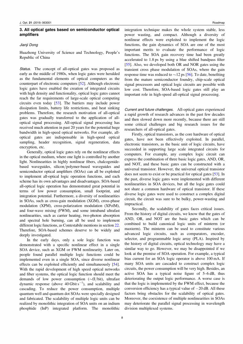
To solve the scalability of optical gates, we offered afeasible solution, where any complex logic circuit can besummed with logic minterm, and each minterm can beimplemented by XGM effects in SOAs [59]. Figure 2 shows acircuit diagram of PLA with a summation of logic minterms.Two channels of input signals are set as the differential phaseshift keying (DPSK) signal (bit A and bit B). These initial bitsare converted into on-off keying (OOK) signals (A, B, A , B ),with a delayed interferometer. Then four sets of logicminterms can be achieved by XGM in SOAs. Finally, thePLA can be controlled and programmed by the couplingarray. Since a lot of semiconductor foundries (i.e. JEPPIX)have offered the fabrication agency of photonic integratedcircuits, these PLA systems can be monolithically integratedon the InP integrated platform with good scalability.
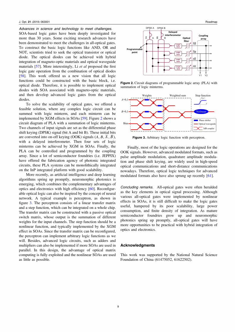
More recently, as artificial intelligence and deep learningalgorithms spring up promptly, neuromorphic photonics isemerging, which combines the complementary advantages ofoptics and electronics with high efficiency [60]. Reconfigur-able optical logic can also be inspired by the concept of neuralnetwork. A typical example is perceptron, as shown infigure 3. The perceptron consists of a linear transfer matrixand a step function, which can be integrated on a whole chip.The transfer matrix can be constructed with a passive opticalswitch matrix, whose output is the summation of differentweights for the input channels. The step function should be anonlinear function, and typically implemented by the XGMeffect in SOAs. Since the transfer matrix can be reconfigured,the perceptron can implement arbitrary logic functions as wewill. Besides, advanced logic circuits, such as adders andmultipliers can also be implemented if more SOAs are used inparallel. In this design, the advantage of optical matrixcomputing is fully exploited and the nonlinear SOAs are usedas little as possible.
Finally, most of the logic operations are designed for theOOK signals. However, advanced modulated formats, such aspulse amplitude modulation, quadrature amplitude modula-tion and phase shift keying, are widely used in high-speedoptical communications and short-distance communicationsnowadays. Therefore, optical logic techniques for advancedmodulated formats also have also sprung up recently [61].
Concluding remarks. All-optical gates were often heraldedas the key elements in optical signal processing. Althoughvarious all-optical gates were implemented by nonlineareffects in SOAs, it is still difficult to make the logic gatesuseful, hampered by its poor scalability, large powerconsumption, and finite density of integration. As maturesemiconductor foundries grow up and neuromorphicphotonics spring up promptly, all-optical gates will havemore opportunities to be practical with hybrid integration ofoptics and electronics.
Acknowledgments
This work was supported by the National Natural ScienceFoundation of China (61475052, 61622502).
Figure 2. Circuit diagrams of programmable logic array (PLA) withsummation of logic minterms.
Figure 3. Arbitrary logic function with perceptron.
9
J. Opt. 21 (2019) 063001 Roadmap

4. Nanoscale all-optical logics
Xiaoyong Hu
Peking University, People’s Republic of China
Status. Even though modern microelectronic technologyhas gained great achievements in high-speed informationprocessing up to several Gbit/s order, there is still anincreasingly tremendous demand for even higher speeds ofmore than several Tbit/s order along with the rapiddevelopment of contemporary information technology,including big data and cloud computing. An ultrahighinformation processing speed of over several Tbit/s ordercould be expected when using photon as informationcarriers. Accordingly, ultrawide-band and ultrahigh-speedoptical information processing chips have been one of theresearch fronts and focus in the overlapped fields ofnanophotonics, materials, and chemistry. Nanoscale all-optical logic devices are essential and key units of opticalcomputing systems, and ultrawide-band and ultrahigh-speedoptical information processing chips. Consequently, fordecades, nanoscale all-optical logic devices have been avery active and important research direction. Great efforthas been put into the demonstration and experimentalrealization of all-optical logic functions. Nanoscale all-optical logic devices can be considered as the counterpart ofphotonics analogous to electronic logic devices used in thecentral processing unit of electric computers. Nanoscale all-optical logic devices can be divided into two categories: thefirst one is a simple logic gate (AND gate, OR gate, NOTgate, and XOR gate, NXOR gate, etc), and the second one isa unit logic device (adder, subtracter, multiplier, encoder,decoder, comparator, discriminator, trigger, shifter, counter,etc). The logic operation using the photon signal is a verychallenging frontier research because of the fundamentalrequirement of very efficient light-control-light. As early as1983, Lattes et al realized the XOR and AND gates using aLiNbo3 Mach-Zehnder interferometer based on the third-order nonlinear optical effect, with an operating light powerup to 2 W [62]. Subsequently, various schemes havebeen proposed to demonstrate all-optical logic devices,including using nonlinear optical crystals, optical fibers,semiconductor optical amplifiers, semiconductor nanowires,photonic crystals, silicon ring resonators, and plasmonicmicrostructures (shown in figure 4) [63–65]. The all-opticallogic devices realized using microcavities, semiconductoroptical amplifiers, nonlinear optical crystals, and opticalfibers have a relatively large size of over 100 μm order,which is not suitable for practical on-chip integrationapplications. The all-optical logic devices realized usingphotonic crystals, silicon ring resonators and plasmonicmicrostructures have a relatively small feature size.However, up to now, the experimental reports ofnanoscale all-optical logic devices are very limited, onlyincluding logic gates, adders, and so on. Moreover, nocomplex all-optical logic function modules, possessing theability of performing various complicated all-optical logic
operations (for example, multiplication and divisionarithmetic logic operation, solving equations and othermathematical operations), have been realized.
Current and future challenges. The fundamental requirementfor all-optical logic functions lies in the realization of efficientlight-control-light. Basically, there are two methods widelyused in all-optical logic devices. The first method is based onthe linear interference, i.e. forming a destructive (orconstructive) interference between two signal lights. Thelogic operation functions realized based on this method aredetermined by the relative optical phase difference of twoinput light signals. On one hand, this method is very simpleand convenient, and very easy to implement, which areobvious advantages. However, the remarkable disadvantageof this method rests with the difficulty of precise control ofthe optical phase difference. As a result, this methodpossesses the inherent instability, and, subsequently, resultsin a low intensity contrast of output logic states ‘1’ and ‘0’ ofless than 6 dB, owing to the poor control of optical phasedifference. This means that this method is not suitable forlarge-scale on-chip integration applications, because thecontinuous accumulation in the errors of optical pathdifference would eventually bring about the ultimate failureof the logic function. So far, only simple nanoscale all-opticallogic gates were realized based on this method. The secondmethod is based on the third-order nonlinear optical effects,which require that the nonlinear optical materials should havea relatively large nonlinear susceptibility and ultrafast
Figure 4. Demonstration of all-optical on-chip logic gates based onsurface plasmon polaritons. Reprinted with permission from [63].Copyright (2012) American Chemical Society.
10
J. Opt. 21 (2019) 063001 Roadmap

response time simultaneously. The advantages of this methodlie in the following two aspects: firstly, this method has stronguniversality, i.e. in principle, all the nanoscale all-optical logicdevices could be realized based on this method. Not onlyhave simple all-optical logic gates been realized by using thismethod, but also complex all-optical devices, includingadders and data distributors, have been realized based onthis method. Secondly, this method has the great potential inthe suitability for practical on-chip integration applications.Therefore, this method has attracted great attention recently.The obstacle limiting the applications of this method is theintrinsic material bottleneck limitation, i.e. the small third-order nonlinear susceptibility of conventional materials, andthe contradiction between the huge third-order nonlinearcoefficient and the ultrafast response time (i.e. the larger thethird-order nonlinear coefficient, the slower the responsetime). This has resulted in a high operating threshold lightintensity of the order of 100MW cm−2 to 1 GW cm−2 for thenanoscale all-optical logic devices. While the practical on-chip integration applications of the nanoscale all-optical logicdevices require a low operating threshold light intensity of theorder of 10 kW cm−2, which has been a great challenge toreach up to now.
Advances in science and technology to meet challenges. Theinherent instability of the linear interference method could bereduced by a certain degree by device miniaturization, benefitingfrom the modern precise microfabrication technique. From theaspect of the present precision of the microfabrication technique,only reaching 10 nm for both the most precise focused ion-beametching technique and electron-beam lithography technique,continuous accumulation in the errors of optical path differencecould not be omitted for the practical on-chip integrationapplications, which still would eventually bring about theultimate failure of the logic function. For the second methodbased on the third-order nonlinear optical effects, the intrinsicmaterial bottleneck limitation could be circumvented in a certaindegree by exploring new nonlinear enhancement methods [66].Resonant excitation is an efficient method to enhance the third-order nonlinearity response of optical materials, even at theexpense of slowing down the time response. Constructingnanocomposite materials, composed of nanoscale noble metallicnanoparticles dispersed in a dielectric matrix, are anotherefficient method to enhance the third-order nonlinearityresponse. The quantum size effect provided by noble metallicnanoparticles has a great contribution to the nonlinearityenhancement. Moreover, the non-uniform distribution of signal
light field in the nanocomposite materials, caused by the hugepermittivity discrepancy between metal and dielectric material,also attributes to the nonlinearity enhancement. For example,recently, an all-optical logic data distributor is realized based onlarge nonlinearity enhancement through resonant excitation viaan upconversion radiative-transfer process in nanocompositematerials. The intensity contrast ratio between the output logicstates ‘1’ and ‘0’ was enlarged to more than 20 dB [66].Plasmonic microstructures have the ability of confining signallight into a subwavelength region, providing an intenseplasmonic field enhancement effect [67]. Therefore, plasmonicmicrostructures provide an ideal platform for the nonlinearityenhancement. New physical mechanisms based on quantumoptics, optomechanical force, exciton-polaritons and even DNAmolecules (shown in figure 5) have also been explored to reachhigh performance nanoscale all-optical logic devices [68–71].
Concluding remarks. Due to the extreme importance ofnanoscale all-optical logic devices for future ultrahigh-speedand ultrawide-band light information processing chips, greateffort has been paid to realize nanoscale all-optical logicdevices with an ultralow energy consumption and ultrafastresponse time. Through exploring novel nonlinearityenhancement approaches, we believe that the intrinsicmaterial bottleneck limitation could be finally overcome.Although the road is bumpy, the future is bright.
Figure 5. By employing the universal recognition properties of DNAsimple photonic logic gates can be created that are capable of AND,NAND, and INHIBIT logic operations. Reprinted with permissionfrom [69]. Copyright (2003) American Chemical Society.
11
J. Opt. 21 (2019) 063001 Roadmap

5. Non-Boolean optically-inspired computing usingspin waves
Gyorgy Csaba1 and Wolfgang Porod2
1Pazmany University, Budapest 2University of NotreDame, IN, United States of America
Status. Wave-based (or interference-based) computing is apowerful concept, and optical computing has attracted muchattention over the years. Challenges remain for computingbased on electromagnetic waves, which include thesignificant overhead associated with conversion between theoptical and electrical domains. However, ideas borrowedfrom optical computing may be applied to other types ofwaves. In this chapter, we focus on implementinginterference-based computing devices using magneticexcitations (spin waves).
Spin excitations in magnetic materials share manycharacteristics with electromagnetic (EM) waves, and maypossibly offer a more compact, integrable and microelec-tronics-friendly implementation for wave-based processing.Spin-wave (SW) based computing is a relatively recent fieldthat is largely motivated by the discovery of new magnetoe-lectronic devices and effects, and by the pursuit ofapplications for these devices in microelectronics [72, 73].
In order to illustrate how a SW-based processor can bederived from an optical structure, an example is given infigure 6. This is an SW-based realization of the Rowlandcircle spectrograph, known in x-ray spectroscopy. SWs aregenerated right on the curved diffraction grating, whichfocuses SWs with different wavelengths to different foci onthe Rowland circle (for details, see [74]). The device layout issimilar to an optical processor, where the light propagatesfrom the source toward detectors via diffracting elements, andthe processing itself is performed by wave interference. Thedifference is that for the SW-based device, the sources anddetectors are electrical structures (i.e. waveguides andantennas), and the SW propagation medium is a patternedmagnetic thin film.
Since the reader of this article will likely be more familiarwith the physics of EM waves than that of SWs, we give abrief side-by-side comparison of them—the similarities anddifferences are the ones that define potential application areasfor SW-based processors.
SWs require magnetic materials to propagate, and weassume ferro- and ferrimagnets for the present discussion, butantiferromagnets would work as well. Magnetic moments(spins) in the material can be excited to perform precessionalmotion. Neighboring spins interact via magnetostatic andexchange interactions, the latter being dominant typically atsubmicrometer wavelengths.
The dispersion relation of SWs depends on the choice ofmagnetic material, the applied magnetic field, and the mode.Most SW modes are strongly dispersive and anisotropic.Typical SW frequencies are in the range of 10–50 GHz,their wavelengths can go all the way down to 10 nm,and propagation speeds are in the 100–1000 m s−1 range.
SW-based devices may match very well to high-speed, microor nanoscale electronic circuitry. The tunability of thedispersion relation by magnetic fields gives extra degrees offreedoms for device design, which are not present in opticalstructures.
In most ferromagnets (especially metallic ones), SWexcitations are strongly damped, and only allow very shortpropagation lengths (on the order of few or few tens ofwavelengths). Magnetic materials with low damping areneeded for practical SW processing devices. A key enablingtechnology for SW-based devices is the availability of low-damping yttrium-iron-garnet (YIG) thin films [77], which is arecent development.
SWs in the linear regime carry very little energy (an orderof magnitude estimate is a few tens of electronvolts energyover a micrometer area of a magnetic thin film). This isbeneficial for low-power processing applications, but makesSW detection challenging.
A key difference between EM waves and SWs is that thelatter show strongly nonlinear behavior for precessionamplitudes beyond a few degrees. Also, SW scattering (oftenreferred to as magnon–magnon scattering) becomes notice-able at higher SW intensities—unlike photons of EMradiation, SWs interact with each other.
Current and future challenges. Challenges primarily are intwo areas of this emerging field: (1) one has to find applicationareas where wave-based processors may compete withestablished electrical solutions, and (2) the lack of efficienttransducers results in a significant overhead formagneteolectronic interconversions. As we will argue below,the two problems are related: in fact, one likely has to look forapplication areas where a relatively complex operation can beperformed using few inputs and outputs, thereby mitigating theoverhead of magnetoelectronic interconversions.
Many SW-based device proposals use wave interferenceto perform Boolean computation [76]. A complete logicsystem, however, requires that logic gates in subsequent statescan drive each other, and this requires amplification betweenthe stages. Amplification of SWs in the magnetic domainwould be extremely useful, but this has turned out to be anelusive goal. Amplification is obviously possible in theelectrical domain, but at the cost of magnetoelectrical
Figure 6. Schematic drawing of a spin-wave-based spectrumanalyzer, as described in [74]. Reproduced from [74]. CC BY 4.0.
12
J. Opt. 21 (2019) 063001 Roadmap
interconversions, which is prohibitive. Considering this, it ishard to imagine that SW-based logic gates will be competitivewith electrical ones. Likely, the same will hold true fortransistor-like switches based on SWs [78]. In our opinion,special-purpose microwave processors (like [74]) are betterapplications as high-speed analog processing is very costly inCMOS circuits, and the overhead of SW interconversionsmay very well be acceptable. Special-purpose non-Boolean orhighly parallel devices and architectures are certainly morepromising than the ones that attempt to directly compete withestablished CMOS solutions [74, 75]. Demonstrating a ‘killerapplication’ remains the Holy Grail for SW device research.
Magnetoelectronic interfaces are the other main chal-lenge. They most straightforwardly use magnetic coupling:the magnetic field of waveguides is used to generate the SWwavefront, and antennas pick up the signal inductively. Fornanoscale (or submicrometer scale) structures, and for short-wavelength SWs, these methods are fairly inefficient. At theinput side, only a miniscule portion of the waveguide fieldcan excite SWs. At the output side, micron-scale structurescollect very little magnetic flux. Typically, much less than apercent of the energy is converted between the electric andmagnetic domains.
Advances in science and technology to meet challenges.Using new physics or smart engineering of magneticmultilayers may boost the efficiency of magnetoelectricinterfaces.
Magnetic fields have to be well localized in order toefficiently couple to short-wavelength SWs, but basicwaveguides create field distributions which are at leastseveral micrometers wide. Fields may be localized by placingfinely-patterned magnetic layers on top of the SW-conductingmedium, as is done in [79] where ferromagnetic nanowires ontop of a YIG film are excited by fairly delocalized waveguidefields and couple the short-wavelength excitations of the YIGfilm. Another avenue is to use spin–orbit torque (spin Halleffect, SHE) as the coupling mechanism—in this case, a spin-polarized current in a thin conductor can directly couple to thespins in the magnetic layer, without the need to createmagnetic fields. Inverse SHE may be used as a read-outmechanism as well, converting SW excitations to a DCcurrent (a mechanism also known as spin pumping). SHE-based devices are an area of active research, but they alsohave potential shortcomings (such as high resistivity in therequired the metallic overlayer).
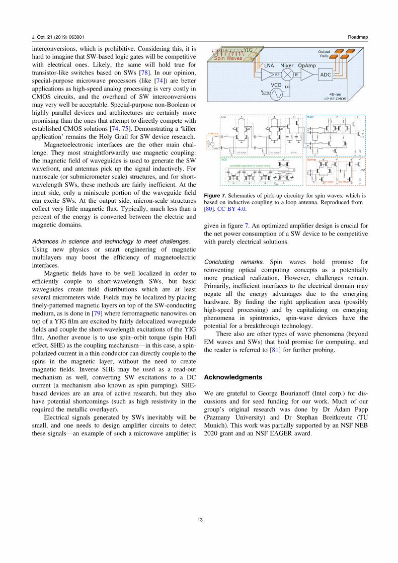
Electrical signals generated by SWs inevitably will besmall, and one needs to design amplifier circuits to detectthese signals—an example of such a microwave amplifier is
given in figure 7. An optimized amplifier design is crucial forthe net power consumption of a SW device to be competitivewith purely electrical solutions.
Concluding remarks. Spin waves hold promise forreinventing optical computing concepts as a potentiallymore practical realization. However, challenges remain.Primarily, inefficient interfaces to the electrical domain maynegate all the energy advantages due to the emerginghardware. By finding the right application area (possiblyhigh-speed processing) and by capitalizing on emergingphenomena in spintronics, spin-wave devices have thepotential for a breakthrough technology.
There also are other types of wave phenomena (beyondEM waves and SWs) that hold promise for computing, andthe reader is referred to [81] for further probing.
Acknowledgments
We are grateful to George Bourianoff (Intel corp.) for dis-cussions and for seed funding for our work. Much of ourgroup’s original research was done by Dr Ádam Papp(Pazmany University) and Dr Stephan Breitkreutz (TUMunich). This work was partially supported by an NSF NEB2020 grant and an NSF EAGER award.
Figure 7. Schematics of pick-up circuitry for spin waves, which isbased on inductive coupling to a loop antenna. Reproduced from[80]. CC BY 4.0.
13
J. Opt. 21 (2019) 063001 Roadmap

SIGNAL PROCESSING FOR TELECOMAPPLICATIONS
6. Optical resonant structures for signalmanipulation
Ghanshyam Singh
Department of Electronics and Communication Engineering,Malaviya National Institute of Technology Jaipur, 302017,India
Status. The nonlinear effects in optical waveguides play avital role in optical signal processing towards switching,multiplexing, compression and logic functions [82]. With theenhanced scope of future possibilities in optical communicationdue to nonlinear effects, the use of nonlinear waveguides, likeresonant cavities, are also increasing due to various advantagessuch as low power requirement and ultrafast switching. Insignal processing operations, resonators provide an efficientway to achieve desirable transfer functions [83], logic [84] andtime delay element [85] in a circuit. Along with this, opticalresonant structures have the benefit of cascadability which canhelp in complex arrangements of circuits. Generally, thedielectric resonators of small size are preferred for integratedoptics while the high index contrast micro-resonators are usedfor microwave applications. It is obvious that at opticalfrequencies, due to non-availability of good conductors, wehave to keep an eye on the radiation losses while designing thelayout of the structures. The structures with high index contrastenable the users to achieve a higher radiation quality factor incomparison to the overall quality factor of the system. Theworries about the quality factor generally having lesssignificance with the high bandwidth therefore resonantstructure came into its own groove once high bit rates werepossible. Along with this, there is a challenge associated withhigh bandwidth, in order to have a low quality factor with highbandwidth acute coupling between the resonator and externalwaveguide is essential and it is generally achieved byevanescent coupling. Coupled optical resonators can be thefoundation of wavelength filters with flat-top responses andthese are largely required in telecom applications. In general,there exist two kinds of resonators; first are ring/rack typeresonators (shown in figure 8) that support degenerate modes oftraveling waves in opposite directions. When index contrast ison the higher side, the radius of rings can be formed smallenough to have lesser radiation losses and higher free spectralrange (FSR). The second are Bragg reflection resonators thathave standing wave modes.
Current and future challenges. Although microring resonatingstructures came into existence in 1969, but the wheel ofintegrated optics structures started rolling when fthe abrication ofdevices operating at 25Gbps and higher emerged in 90s.
In the early 90s for high frequency applications (25 GHzand higher), sixth order fabrication of resonating cavities tookonly a single lithographic step. In comparison to that,
commercial filters could only be fabricated up to a fourthorder at that time for such high frequencies. There weremainly two challenges in designing high quality factorresonating structures. The first was to find a high indexcontrast material which can be used to fabricate waveguidesand the second was to develop a very narrow gap between thering and the linear waveguide, which is necessary for efficientcoupling of input waveguide to output waveguide ofresonating structures. An optical resonant structure finds lotsof applications in optical signal processing by virtue of itsvarious qualities like low loss, large FSR, signal generationand conversion [86, 87]. In the current decade, a realchallenge has been to optimize these attributes. In the latterhalf of the 90s, the fabrication of optical resonant filters fromglass was reported several times with promising results, buthad limitations in the form that it was necessary to arrangevertical coupling from the input port to drop port as shown infigure 8 for the efficient resonance effect [83]. Thereafter,during the beginning of the current century, optical resonatorswith semiconductor materials have been reported which havebetter nonlinear characteristics [84] and it was also possible tofabricate the ring radius as small as 2.5 μm with quite a highquality factor value of 10 000 and with very tightly confinedsemiconductor waveguides [84]. With the advent of highprecision fabrication techniques, the resonant cavities nowhave various configurations like all pass and band pass filtersand the spectra of real-time application has also broadenedwith biosensing [88], switching [83], logic function andwavelength conversion [86]. During the last decade, a greatamount of work has been reported explaining variousapplications of resonators in signal processing. Heebneret al gave various transmission characteristics of opticalsignal in resonators; they also explained the construction oftunable time delay circuits as an application of opticalresonators [85]. Researchers from the institute of Electronics,National Academy of Sciences, Belarus, were able to presentanalog to digital data conversion at a faster rate successfullyusing optical ring resonators, in which multiple wavelengthswere provided from the input waveguide and that too with thering radius of around 10 μm with time response of 10 ps [86].The analog signal is used as a control signal that changes thefree carrier density of the semiconductor resonator wave-guide, thus changing its refractive index. This signal could beboth optical and electrical. In all-optical analog–digitalconverters, the optical analog signal with variable intensityfalls on the top surface of the micro-resonator. The challengeof maintaining faster switching in this design has beenachieved by appropriate switching the contrast with highconversion frequency [86]. The prospect of increasing theswitching speed of the resonant cavity has just been the tip ofthe iceberg of opportunities for broadband communication,satellite communication and many other techniques. Alongwith this, Yupapin and Suwancharoen demonstrated thegeneration and cancellation of chaotic signals [87], which
14
J. Opt. 21 (2019) 063001 Roadmap

were employed to enhance the security of information signals,thereby enabling the prospect of increasing the number ofusers for a system. Later, Ramachandran et al proposed bio-sensing applications of micro resonant structures [88].Recently, Ali et al demonstrated a microring resonatorstructure [89] suitable to produce squeezing light and foundits application as an oscillator in signal processing. There arelot of scope and applications available in optical resonatingstructures. In the current scenario, the major challenges forresearchers remain to decrease the size of ring cavity and tolower the cavity gap. Another important task is to increase theswitching speed of the resonant cavity, which may furtherincrease the capacity of whole system. With recent advancesin the field of chip fabrication and/or very large scaleintegrated (VLSI) designs, the challenges to fabricate theresonating structures with low radius and low cavity gap havebeen met to come up with the newer devices with very highprecision and reduced size. This article also further discussesthe advancement in technologies to face the challenges in thefield of optical resonating structures.
Advances in science and technology to meet challenges.This section will discuss the advancement in technologies forthe implementation of various applications of resonatingstructures. The fundamental need for the development ofresonant cavity is to choose the material that possesses a largeindex contrast so as to allow the fabrication of rings below100 μm. The advancements in fabrication techniques likesputtering and reactive ion etching could lead to theproduction of a fine resonant structure. To cover the entireoptical window (850 nm to 1550 nm), the radius of the ringresonation also needs to be decreased for the verticallycoupled resonant structure. Further advancements encouragedcompact resonant structure fabrication and led to the cavitylifetime order of picoseconds. Thereby, the wavelengthconversion power and switching power got reduced. Alongwith this, the availability of resonant structure in the ring size
of 10 μm could lead to the practical implementation of theresonant cavity for information protection. The microringresonant structures, fabricated using the dielectric, resulted indeveloping various biosensing surfaces as well, though thesesurfaces, fabricated using photolithographic techniques,remained susceptible to VLSI technology. Some researchershave demonstrated resonant structures fabricated with theamorphous and polycrystalline silicon platforms [90], whichhave shown promising characteristics for signal processing.With the introduction of resonant cavities in an add dropconfiguration, the pump and probe method can now be usedto route an incoming signal to the drop port of the device inaccordance with the control beam. Youplao et al haverecently proposed a model with a successive microringpumping technique to produce an amplified output signal forfree space communication [91]. Alongside this, researchershave reported developed electronic devices like modulators,amplifiers and oscillators using microresoant structures, andthese devices can be further optimized for high speed andcascadable circuits for light fidelity (LiFi) and other free spacecommunication applications.
Concluding remarks. This section briefly narrates theoperation and application of optical resonant structures forthe manipulation and transmission of optical signals. I haveincluded the major challenges that have been faced byresearchers and scientists in the journey of developingrelevant technologies. The aim of this review has been todiscuss various development stages of optical resonantstructures and their importance for optical signaltransmission. I have also reviewed the way resonantstructures are used to perform switching and logicoperations to implement important applications such asbiosensing, wavelength and analog to digital conversions. Inaddition to details mentioned herein, the vital role ofelectronic devices (LED for the inputs, photodetectors at theoutput) has also been reported in the development of completecircuits with resonant structures.
Acknowledgements
I appreciate the work done by all the referenced authors fortheir contribution in the field of optical resonant structure andits various applications. I am also thankful to my institute(MNIT Jaipur) for providing research facilities and technicalinfrastructures to work in this direction.
Figure 8. Generic layout for a vertically coupled ring resonatorstructure.
15
J. Opt. 21 (2019) 063001 Roadmap

7. Optical regeneration
Alan E Willner1 and Ahmed Almaiman2
1University of Southern California, CA, United States ofAmerica2King Saud University, Saudi Arabia
Status. Signal regeneration is primarily aimed at improvingthe quality of a transmitted signal. Regenerators are designed toincrease system performance, reduce data degradation, extendsystem reach, and enhance the signal-to-noise (SNR) for higherlink capacity. In general, regenerators perform three signal-processing regeneration functions (i.e. ‘3R’): (1) reamplifying,(2) reshaping, and (3) retiming the signal [92]. Conventionally,signal regeneration in an optical system is performed thoughoptical-electrical-optical (OEO) conversion, in which a weakand distorted signal is detected, restored in electronics, andretransmitted onto an optical fiber.
Recently, there has been growing interest in fullyregenerating optical signals in the optical domain. There aremany potential advantages of all-optically regenerating thesignal such as: high efficiency by avoiding OEO conversion,fast processing, large bandwidth, and ability to operate on thesignal phase. Although ‘1R’ optical regenerators (or ampli-fiers, such as erbium-doped fiber amplifiers, EDFAs) havebeen deployed worldwide, they allow the data to becomedistorted in shape and time. Such distortions are much morecomplicated to regenerate all optically.
Advances in optical communication technologies andgrowth in demand for higher capacities have opened up newopportunities for all-optical regenerators. For example, thetechnology of optical transceivers has developed to simulta-neously tailor the optical wave in multiple dimensions:amplitude, phase, time, frequency, polarization, and space.Dual-polarization and higher-order, phase-and-amplitude-basedmodulation formats for wavelength-division-multiplexed (WDM)channels are currently being adopted in many fiber systems [93],and space-division-multiplexing (SDM) is of great currentinterest [94]. Such channels impose additional transmissionchallenges, requiring higher SNR and lower data degradation.
Optimally, optical regenerators should operate on multi-ple dimensions of modulated signals, as shown in figure 9.Recent reports have investigated using optics for regeneratingthe following signals: (i) multiple amplitude levels [95], (ii)multiple phase levels [96], (iii) WDM channels with binarydata [97], (iv) channels degraded by polarization-modedispersion [98], (v) WDM channels with crosstalk [99], and(vi) SDM channels [100]. These demonstrations were enabledby various novel linear and nonlinear optical devices. Forexample, all-optical phase regeneration can be accomplishedby coherently adding the signal to the conjugate of its higherharmonics using four-wave mixing to create a staircase phasefunction, as shown in figure 10.
Current and future challenges. Some current and futurechallenges for efficient all-optical regenerators include thefollowing:
(1) Optical regeneration should be modulation format andbaudrate transparent. Next generation optical networks areadopting flexible and modulation format variable transceivers.Any dependence on modulation format will reduce theefficiency and upgradability of the regenerators. It is currentlyvery difficult to achieve a generic ‘black-box’ regenerator forall types of modulation formats and data channels.
(2) Optical regeneration should improve the optical SNRby: (i) amplifying only the data signal, and (ii) reducing thesignal’s amplified spontaneous emission (ASE) noise; ASE
Figure 9. Concept of the future all-optical regenerator to recover all-dimensions of an optical wave such as amplitude, phase, frequency,time, polarization, and spatial mode.
Figure 10. Experimental phase regeneration of 10 Gbaud BPSK andQPSK channels by coherently adding the signal to conjugates of thehigher harmonics. Error vector magnitude = EVM [101].
16
J. Opt. 21 (2019) 063001 Roadmap

arises after a signal passes through 1R EDFA regenerators.This can be challenging for advanced data modulationformats. In addition, the optical regenerator should mitigateany crosstalk and inter-symbol interference that arises in thedifferent domains of the optical wave, such as wavelength,polarization, and spatial modes.
(3) Optical regeneration should be capable of simulta-neously regenerating multiple WDM independent datachannels, which is possible given the wide bandwidth ofoptics as compared to electronics. This feature may justify theeconomics of using a single optical solution to replace manyelectronic regenerators.
(4) Power consumption of optical regeneration should bereduced to become lower than electronic solutions. Forinstance, the nonlinear mixing efficiency in the χ2 or χ3
materials requires relatively high pumping power levels,especially when generating higher order mixing terms orprocessing multiple channels. The limited conversion effi-ciency may hinder overall system power efficiency. More-over, lower conversion efficiency could result in additionalpower loss and increased noise figure.
(5) Future optical regeneration techniques should notresult in inefficient utilization of the available spectrum. Forexample, transmitting pilot tones or signal copies might assistin regenerating multiple higher-order modulation channels,but the extra bandwidth wasted may offset the systemimprovement.
Advances in science and technology to meet challenges.With the aforementioned challenges, many advances wouldgreatly benefit the future of optical regenerators to enableefficient operation for potential deployment. Some advancesinclude the following:
(1) Advances in developing optically-enabled mathema-tical techniques capable of regenerating the higher-orderquadrature-amplitude-modulation (QAM) signals with mini-mum complexity, higher efficiency, and fewer numbers ofstages would be highly beneficial. These methods may exploitvarious novel phase-sensitive wave-mixing approaches. Areported multi-stage solution for regenerating higher-orderQAM signals is to demultiplex the higher-order signal intomany lower-order channels (e.g. quadrature phase-shift-keying, QPSK), regenerate each signal independently, andadd the lower-order signals coherently. However, performingthe regeneration process in a single stage would be moreefficient.
(2) Advances in optical regenerators should incorporatehighly-complex functions using optical tapped-delay-linefiltering to recover the pulses into their original shape. Forexample, the bandwidth of Nyquist-shaped pulses is similar tothe signal’s baseband bandwidth. These shaped pulses onlycarry the symbol at the exact sampling time, and appear as‘random noise’ to the receiver elsewhere in time. If an opticalregenerator did not preserve the shape of pulses, it mightresult in increased signal bandwidth, which could causeoverlap in between adjacent WDM channels.
(3) Optical frequency combs have enormous potential toadvance future optical regeneration systems. A frequency combprovides multiple, mutually-coherent, phase-locked frequencylines that are equally spaced. These frequency lines are anabundant source of pumps and mixing waves for linear andnonlinear processes in an optical regenerator. Future researchshould explore the full benefit of using multiple comb lines asopposed to multiple discrete laser sources.
(4) Advances in photonic integration circuits (PICs) candramatically enable compact, cost-effective, low-powerregeneration systems that utilize multiple linear and nonlinearoptical stages on a single chip. Recently, integrated nonlineardevices have been utilized to demonstrate regenerationfunctions [102, 103]. However, a fully packaged regenerationsystem in a PIC form that could perform linear and nonlinearprocesses with different functionalities would be a large steptowards practical deployment.
(5) Future power-efficient optical regeneration systemsshould exploit advances in highly-nonlinear material andnovel metamaterials. In particular, the field of metamaterialshas exhibited many significant recent advances in makingextremely-small and highly-nonlinear devices. These materi-als could potentially provide novel light–matter interactionswith higher-order chirality beyond the conventional x2 and x3
and with higher nonlinear efficiency. Future research shouldconsider utilizing these novel physical properties to achievelow power consumption.
(6) Single-photon quantum systems have the inherentproblem of the ‘no cloning theory’, making even 1Rregeneration a highly significant challenge. Advances in anyform of regeneration of single photons could have anenormous impact on future quantum communication systems.
Concluding remarks. Unlike full OEO-based regenerators,the all-optical regeneration solutions in communicationsystems may not need to fully ‘clean-up’ the signal orcompensate all impairments for an unlimited number ofpasses. Instead, it may be sufficient for an optical regeneratorto help significantly extend and maximize a given system’sperformance. Thus, it could be acceptable not to address someof the impairments that might be ultimately compensated atthe receiving end of the link.
If cost-effective, low-power, data-transparent, on-chipoptical regenerators can be demonstrated, the performance offuture optical systems might leap-frog today’s systems indeployment, practicality, and performance.
Acknowledgments
Center for Integrated Access Network (CIAN); (Y501119);National Science Foundation (NSF) (ECCS-1202575); Van-nevar Bush Faculty Fellowship program sponsored by theBasic Research Office of the Assistant Secretary of Defensefor Research and Engineering and funded by the Officeof Naval Research (ONR) (N00014-16-1-2813); FujitsuLaboratories of America (FLA); Futurewei Technologies Inc.
17
J. Opt. 21 (2019) 063001 Roadmap

8. Kerr nonlinear waveguides for telecom-orientedall-optical signal processing
Victor Torres-Company and Jochen Schröder
Department of Microtechnology and Nanoscience, ChalmersUniversity of Technology, SE 41296 Gothenburg, Sweden
Status. Fiber-optic communication systems form the backboneof the internet. The data rates and information communicationservices that we enjoy today are enabled by breakthroughtechnologies developed over the last 40 years. The field startedwith the low-loss silica fiber in the late 70s; the advent of theerbium-doped fiber amplifier (EDFA) led to wavelengthdivision multiplexing (WDM) in the 90s; and culminated inthe high spectral efficiencies enabled by advanced coherentmodulation and digital signal processing (DSP) and powerfulcoding we see today. Lightwave communications have maturedto a point where commercial WDM systems can routinelytransmit digital data at multi-terabit per second rates.
Notwithstanding, the spontaneous emission noise in theEDFA and the ultrafast nonlinear Kerr response of standardsingle-mode silica fibers place fundamental limits on themaximum data rate that can be transmitted over a fixed link,leading to concerns that the fiber capacity will soon be exhaustedwithout further technological innovation [93]. This situation hasspurred a renewed interest in fiber technologies [104] andnonlinear optical signal processing functionalities, such asparametric phase-sensitive amplification [105], optical regenera-tion [106] and nonlinearity compensation [107]. Arguably, therole of optical signal processing in future telecom applications isto alleviate the distortions experienced by the optical signals uponpropagation in the fiber link and facilitate functionalities thatwould be very difficult, if not impossible, to realize by electronicDSP alone. Here, we restrict the scope to nonlinear signalprocessing based on the Kerr effect. Paradoxically, this very samephenomenon can be harvested to our advantage in a materialplatform to combat its detrimental effects in the silica fiber.
Current and future challengesIllustrating the challenges with Kerr nonlinear waveguides: thePSA example. The case of the phase-sensitive amplifier (PSA)[105–107] illustrates in a clear manner the potential of nonlinearsignal processing for telecom applications. In contrast toconventional amplifiers based on stimulated emission, a PSArelies on the parametric interaction among three waves mediatedby the Kerr effect in a nonlinear waveguide. A PSA canapproach a noise figure of 0 dB, meaning that the signal can beamplified without introducing additional noise. By properengineering the waveguide dispersion, the PSA bandwidth canbe significantly broader than what is possible with an EDFA.
The demonstrations in [105–107] were implemented in anonlinear fiber. This fiber displays incredibly low absorptionlosses but it is difficult to precisely control the dispersionprofile along the propagation length. In addition, Brillouinscattering and other deleterious effects place a limit on theoptical power that can be efficiently utilized for the Kerreffect.
Nanophotonic waveguides allow for a very strong opticalfield confinement. If, in addition, the core is made of a materialwith large Kerr coefficient n2, the waveguide will feature adramatic enhancement of the Kerr parameter [103,108–111].This has enabled a plethora of signal processing functionalitiesin a compact platform. These waveguides are fabricated withadvanced lithographic techniques that provide an exquisitecontrol of the cross-section dimensions and in turn of thedispersion characteristics. Indeed, PSA has been demonstrated indiverse integrated platforms (see, for example, [112]), althoughonly with a pulsed pump wave. The experiments in [105–107]operated with a continuous-wave laser pump. This is moresuitable for practical telecom-signal operation but places atremendous challenge on the nonlinear phase shift per unitpower that needs to be achieved in the nonlinear waveguide.
State of the art in Kerr nonlinear waveguides. Ideally, anintegrated waveguide platform should give a nonlinear phaseshift of γ·Leff·Pcw∼π, where γ represents the nonlinear Kerrparameter (in units of [Wm]−1), Leff is the effective length of thewaveguide and Pcw the continuous-wave power. In the case of aPSA, this would roughly yield an on-chip parametric gain closeto 10 dB. Since Pcw is somewhat limited to 0.1W for state of theart on chip laser sources, the relevant figure of merit becomesthe amount of nonlinear phase shift per unit power, resulting inthe target γ·Leff∼10 π [W]−1. This discussion obviates thefact that many of these platforms display nonlinear absorptioneffects (such as two and three-photon absorption, free carriereffects, etc) which place an even lower limit to the amount ofPcw that can be safely delivered to the waveguide.
Table 1 illustrates the challenge. It summarizes thenonlinear and linear performance of diverse state-of-the-artnonlinear waveguide platforms. The message is clear: thewaveguide platforms that feature higher nonlinear Kerrparameters display a higher amount of linear and nonlinearloss. These are all extremely interesting materials but furtherwork is needed to achieve the ultimate goal of an integratednonlinear waveguide platform with negligible nonlinear lossin the telecom band and sufficient nonlinearity and low loss.
Advances in science and technology to meet challenges.Silicon nitride is a dielectric material with a transparencywindow that ranges from the visible to the mid IR. In itsstoichiometric form, it has nonlinear Kerr coefficient that isabout ten times higher than silica. High-confinement siliconnitride resonators display an equivalent loss down to the1 dBm−1 [108] but the material absorption itself is about anorder of magnitude lower. This material platform is superb fornonlinear optics in the near infrared because of its absence ofnonlinear loss. The path forward towards on-chip parametricgain with continuous-wave pumping in this platform requiresfurther understanding of the origin of the absorption losses andthe development of advanced etching techniques to be able torealize ultra-smooth sidewalls in very long (>1m) waveguides.The device will naturally occupy a bigger area. Interestinglyenough, the nonlinear Kerr coefficient can be preciselycontrolled with the film stoichiometry. In particular, silicon
18
J. Opt. 21 (2019) 063001 Roadmap

rich silicon nitride (SiRN) [109, 113] provides a dramaticenhancement of the Kerr effect, but this is accompanied by adecrease in the optical bandgap and an increase in the linear loss.Although the bandgap is large enough to avoid two-photonabsorption (TPA) in the telecom band (see figure 11), it is stillunclear the extent to which three-photon absorption (3PA) andassociated carrier dynamics may affect the nonlinearperformance in practical applications. Furthermore, the originof the absorption losses is not well understood either.
Silicon rib waveguides can be engineered with p-i-ndiodes to remove photogenerated carriers and decrease freecarrier absorption losses. Recent demonstrations based on ribwaveguides have allowed for efficient wavelength conversionand regeneration [110]. Nonlinear losses due to two-photonabsorption remain, although the key challenge in thisgeometry is the control of dispersion.
Recent advances in AlGaAs bonded on an oxidizedsilicon wafer have allowed to achieve strong optical fieldconfinement in nanowire waveguides, leading to hugenonlinear Kerr parameters [111]. The atomic composition ofthis semiconductor can be controlled with great accuracy,allowing for precise control of the optical bandgap. Recentresults indicate absence of TPA [111], but similar to the caseof SiRN, the effects of 3PA are not well understood yet.
Another interesting development is with hydrogenatedamorphous silicon [103]. This material platform has an increasednonlinear parameter and optical bandgap than its crystallinecounterpart. It still displays nonlinear losses, but the mostintriguing aspect is the reported time instability (samples degradeover time), whose physical origin is also not well understood.
Other relevant material platforms include tantalumpentoxide, chalcogenides, plasmonic focusing, polymers anddiverse semiconductor materials such as gallium phosphide.The tradeoffs are similar to the ones observed for the materialplatforms in table 1 however, namely higher nonlinearcoefficients are obtained for platforms that display an increasein both linear and nonlinear losses.
From a more practical perspective, it is important toremember that these waveguide structures will require co-integration with pump lasers and interfacing with low-lossnanophotonic circuits and possibly electronics. Other potentialconcerns such as damage power thresholds and the nonlinearresponse in complex integrated circuits deserve more attention.
Concluding remarks. Nonlinear signal processing can providesignificant gain benefits in telecom applications. For practicaldeployment, it would be necessary to realize an integrated
nonlinear platform that allows to achieve a nonlinear phase shiftper unit power close to 10π and has no sign of nonlinear loss.Unfortunately, most material platforms either display stronglinear and nonlinear loss or insufficient Kerr parameter. If thisbreakthrough were achieved, it would have far reachingconsequences not only in fiber optical communications, butalso in quantum optics, spectroscopy and metrology.
Perhaps the wonder nonlinear material is just around thecorner or perhaps we should focus on exploring differentwaveguide structures. For example, an interesting alternativethat has not been carefully investigated in the literature to ourknowledge is the possibility of a hybrid nonlinear waveguidethat provides optical amplification around the pump windowto compensate for the detrimental effects of the linear loss.On-chip net gain in glass waveguides doped with rare-earthelements have been reported, but little is known about theirnonlinear Kerr coefficients.
Acknowledgments
We acknowledge the support of the Swedish Research Counciland the European Research Council (DarkComb GA 771410).
Figure 11. (a) Scanning electron microscope image of the cross-section of one of our SiRN waveguides. (b) Simulation of modeconfinement in the structure when the waveguide core is claddedwith silica. (c) Efficient supercontinuum generation in the wave-guide. Massive broadening is obtained with sub kW femtosecondpulses delivered from a fiber fs oscillator. These results indicate thatan efficient nonlinear response can be attained with moderatenonlinear Kerr parameter but sufficiently low linear loss andnegligible nonlinear absorption. Results adapted from [113].
Table 1. Overview of recently developed nonlinear waveguide platforms [103, 108–111] with a large nonlinear Kerr parameter, γ; u.i. means‘under investigation’.
Platform γ (W.m)−1 Linear loss (dB m−1) γ·Leff(W)−1 Nonlinear loss?
SiN ∼1 ∼1 ∼1 noSilicon rich SiN ∼500 ∼450 ∼5 u.i.Si with pin 280 ∼100 ∼10 yesAlGaAs 660 140 ∼20 u.i.Amorphous Si:H 2975 ∼320 ∼40 yes
19
J. Opt. 21 (2019) 063001 Roadmap

9. Nonlinear all-optical processing in silicon corefibres
Anna C Peacock
University of Southampton, Southampton, United Kingdom
Status. Despite the excellent transmission properties ofsilica glass, there has long been a desire to fabricate fibresfrom new materials that can offer enhanced optical processingcapabilities and/or extended transmission windows [114].Although most efforts in this area have focused on non-silicaglasses, such as the heavy metal fluorides and chalcogenides,over the past decade, a new class of fibre with silicon corematerials has appeared [115]. These fibres are still clad insilica so that they are robust, stable, and can be handled in asimilar way to the pure silica structures. However, the largenonlinear coefficients and tight mode confinement offered bythe high index silicon core (as discussed in section 14)presents exciting opportunities for the development ofcompact and efficient all-optical processing devices thatcould be seamlessly integrated within existing fibrecommunications networks.
The first example of a silicon core fibre was produced in2006 by a modified chemical vapour deposition (CVD)technique. In this approach, the silicon materials wereincorporated inside pre-existing silica templates, such ascapillaries and microstructured optical fibres. However, onlytwo years later, a second technique was developed thatallowed for the large scale production of silicon fibres via aconventional drawing tower approach, significantly enhan-cing their practicability. This method involves sleeving thesilicon material inside a silica cladding to form a preform,before drawing it into a fibre with micron-sized dimensions.Importantly, these two fabrication techniques are comple-mentary in terms of the materials and geometrical structuresthat can be accessed. For example, the CVD approach hasbeen used to produce hydrogenated amorphous silicon (a-Si:H) fibres with the smallest core dimensions (a few microns orless) over centimetre lengths, while the drawing method hasproduced large core (tens of microns or larger) crystallinesilicon fibres over hundreds of metres.
From a nonlinear perspective, a-Si:H has a higher Kerrnonlinear coefficient than crystalline silicon, usually reportedto be around five times larger. Thus, when combined with thesmaller core diameters, as of to date, the a-Si:H fibres havebeen the most suitable for nonlinear device demonstration.Figure 12 shows examples of two basic all-optical processingfunctions, (a) modulation and (b) wavelength conversion, thathave been used to benchmark the performance of these fibres[115]. In both cases, the a-Si:H fibres had a core diameter of∼6 μm, so that they exhibited strong normal dispersion in thetelecoms band, and a length of ∼1 cm. The first demonstra-tion made use of a cross-absorption modulation (XAM)process, whereby a high power pump pulse was used toimprint a dark pulse on a CW signal via two-photonabsorption (TPA). The second scheme was based on cross-phase modulation (XPM), whereby the pump was used to
impart a wavelength shift (blue then red shift as indicated bythe dashed white line) on a weak probe. In both cases, thetimescales for the modulation were on a sub-picosecond scale,with an extinction ratio greater than 4 dB (as high as 12 dB inthe case of the XPM red shift). Although the nonlinearperformance of these fibres was shown to be comparable towhat has been achieved in nanoscale planar analogues, thepowers required to observe these effects were higher owing tothe larger cores (hundreds of watts compared to milliwatts).However, a simple way to reduce the power requirements isto use these structures in a resonator geometry to enhance thelight–matter interactions, similar to what has been achieved inpure silica fibres [116]. By coupling light into the silicon coresuch that it is confined to circulate in a whispering gallerymode configuration, it has been shown that the powerthreshold for all-optical modulation can be reduced by fourorders of magnitude [117].
Although much of the early nonlinear optical character-ization of these fibres was focused on the telecoms band,owing to the strong nonlinear absorption of silicon in thisregion, interest soon shifted to longer pump wavelengths. Aswell as mitigating the effects of TPA, moving the pump intothe mid-infrared region (i.e. λ>2 μm) has the addedadvantage in that it is possible to access the anomalousdispersion regime, even in a micron-sized core. Figure 12(c)shows two examples of continuum generation obtained in a2 μm diameter core a-Si:H fibre with a length of 4 mm; onepumped in the normal dispersion regime (λp∼1.8 μm bluecurve) and the other in the anomalous regime (λp∼2.5 μmred curve) [118]. Note, the black dashed spectra areillustrative of the input pump. Clearly, the latter processgenerates the broadest continuum, octave-spanning over
Figure 12. (a) All-optical modulation and (b) wavelength conversionin a silicon core fibre. (c) Supercontinua generated via pumping indifferent dispersion regimes.
20
J. Opt. 21 (2019) 063001 Roadmap

1.6–3.4 μm, but at the price of reduced flatness andcoherence. Nevertheless, these results pave the way forsilicon core fibres to find application in high-speed all-opticalregeneration and spectral slicing for wavelength divisionmultiplexing within all-fibre integrated systems.
Current and future challenges. As with any new devicetechnology, there are a number of challenges that must beovercome in order to improve the applicability of the siliconcore fibres. For nonlinear processing, perhaps the mostimportant of these is the reduction of the transmission losses.Figure 13 highlights the progress that has been made over thepast decade to enhance the transmission properties in both theamorphous and crystalline materials. In terms of the a-Si:Hmaterial, improvements must be achieved through thecomplex deposition process, which is somewhat limitingand hence why progress is currently stalled around the1 dB cm−1 mark. In contrast, many of the advancements thathave been made within the crystalline core materials can beattributed to novel post-processing techniques that have onlyrecently been developed, and thus work in this area is stillvery much ongoing [119].
Related to this issue is the role of nonlinear loss on theperformance of the devices. This is something that cannot bemitigated entirely, but it can be minimized by working in aregime where the nonlinear loss coefficients are small, asdemonstrated in figure 12(c). However, consideration shouldalso be paid to the choice of system parameters, includingpump pulse duration, peak power, and repetition rate toreduce the build-up of free carriers, the effects of which canbe seen in the slow recovery in figure 12(a). When working inthe telecoms band, it is quite likely that carrier sweep outschemes will need to be employed for high-speed (GHz)systems.
From a more practical point of view, another keychallenge to be addressed is how best to interface the highindex silicon core fibres with the low index silica structures tominimize the coupling losses and improve the robustness ofthe systems. Coupling and packaging is also one of the majorissues facing chip-based silicon photonics [120]. However,owing to the similar geometry and the vast amount of prior-artthat has been developed for fibre-to-fibre coupling, there is amuch clearer route towards tackling this problem for thesilicon fibres and progress is well underway [121].
Advances in science and technology to meet challenges.The most obvious route to advancing the silicon fibreplatform is to optimize the core materials and dimensions,both of which are achievable using well-developed fibre post-processing techniques.
The first major advance in this area was obtained using alaser to heat and melt the silicon core material so that itcrystallized on cooling [122]. The precise nature of thecrystallization and the effect it has on the material propertiesdepends on the phase of the starting core material (amorphousor crystalline), as well as the cooling dynamics, but in allcases a reduction in the losses has been observed [119, 122].
Significantly, when the starting material is amorphous, thechange in volume of the core induces a strain, which can beused to alter the optoelectronic properties of the fibre [122].Furthermore, as this process can be highly localized, it opensup a path to modifying the properties of the core at preciselocations along the length, so that different device functionscould be achieved in a single fibre (a desirable advanceidentified in section 12).
An alternative approach that is being pursued is based ona conventional fibre tapering procedure, which involvesheating and stretching the fibres to reduce their core/claddingdiameters. Similar to the laser processing procedure, as thecore cools it crystallizes to result in an improvement in thetransmission properties. However, the ability to alter the coresize during the processing also allows for simultaneoustailoring of the dispersion and nonlinear properties. As aresult, this approach has recently produced the first low-loss,small core crystalline silicon fibre capable of supportingnonlinear propagation [123], a clear indication that all-opticalprocessing functionality in these fibres is on the horizon.
Concluding remarks. Although still a nascent technology,silicon core fibres are already showing promise for nonlinearall-optical processing. A key advantage of this platform overthe standard silica fibres is that the processing can be achievedover very short lengths and with relatively low opticalpowers. They also offer an extended transparency windowinto the mid-infrared, where there is the potential for them tobe applied in applications such as sensing, spectroscopy andmedical surgery. In terms of improving their practicality,reducing their loss values, ideally towards the ∼1 dBm−1
level, remains the most critical challenge, and should be a keytarget for the community over the next few years. Once thismilestone has been achieved, it is easy to predict that anumber of exciting nonlinear possibilities will be unlockedfor the silicon core fibres.
Acknowledgments
The author acknowledges EPSRC for support through herresearch fellowship.
Figure 13. Progress to reduce the losses in the amorphous andcrystalline silicon core fibres.
21
J. Opt. 21 (2019) 063001 Roadmap
10. Novel silicon photonic devices and processes
Michael J Strain
University of Strathclyde, Glasgow, United Kingdom
Status. Silicon photonics has been extremely successful as aplatform for chip-scale optics, with the technology nowwidely available through a number of international foundries.The key benefits of the platform include its low propagationlosses at telecommunications wavelengths, high confinementof the optical field to sub-micron waveguide cross-sections,compact device footprints, and compatibility with electronicmanufacturing processes. These properties have enabled therealization of a wide range of compact, on-chip linear opticalcomponents including wavelength selective filters, powercouplers, interferometers and delay lines. In turn, these simplebuilding block components have been used to construct largescale photonic integrated circuits (PICs) to perform opticalsignal processing functions such as temporal integration anddifferentiation [124]. Direct integration with electronics hasallowed active feedback and control of optical signals [125],while hybrid materials integration has enabled functionalitybeyond that of silicon alone, for example, efficient on-chiplight generation [126].
Further functionality has been enabled by the native χ(3)
non-linearity of silicon, with demonstrations of all-opticalsignal processing operations such as signal broadcasting,regeneration and switching [127]. Furthermore, degeneratespontaneous four-wave mixing in micro-resonators is nowcommonly used as an on-chip source of correlated orentangled photons for quantum optics systems [128].
Current and future challenges. Although a wide range offunctions have been demonstrated on the silicon photonicsplatform, there remain a number of key challenges in thedevelopment of systems for all-optical processing.
1. Tuning and trimming. Non-linear effects in siliconwaveguides can be strongly enhanced by confining the field tosmall volume, high Q-factor resonators. The optical propertiesof such resonators, for example resonant wavelength, arestrongly dependent on fabrication tolerances. Stable operationwith respect to an external source requires post-fabricationtrimming or in situ active control of the device, especiallywhen using coupled arrays of devices.
2. Efficient χ(3) processes. Third-order non-linear opticaleffects in silicon have been demonstrated for applicationsfrom all-optical switching to super-continuum generation.Nevertheless, at telecommunications wavelengths, two-photon absorption (TPA) losses and associated free-carrierdispersion and loss are severely limiting effects in the efficientuse of Kerr non-linearities in silicon. Methods by which thesenon-linear losses can be reduced or avoided are crucial, e.g.by operating at wavelengths beyond the two-photonabsorption limit.
3. Access to χ(2)effects. Silicon does not exhibit a nativeχ(2) non-linearity that would enable applications includinghigh-speed, low noise modulators, spontaneous parametricdown conversion sources and difference frequency generation.
4. Rejection of on-chip pump light. Many of the non-linear processes used in silicon photonic systems require astrong pump source. Once the non-linear process has beencarried out, it is then desirable to separate the pump light fromthe propagating signals coupled to further PIC sub-systemsdownstream. For quantum optics applications, the necessarypump rejection is often required to be over to 90 dB.
5. Manufacturing at scale. Any technology developed toenable all-optical processing on silicon photonic chipsrequires to be scalable in order to be compatible with thepotential for volume manufacture that is a key advantage ofthe silicon platform. Furthermore, as silicon PICs increase incomplexity, the footprint and number of individualcomponents integrated onto these chips will also increase,demanding a high yield manufacturing process.
Advances in science and technology to meet challenges.Electrically addressable tuning of photonic devices has beenenabled using both thermal and p-i-n junction technologies insilicon. These schemes are further enhanced by feedbackcontrol [125], especially where direct integration with siliconelectronic drivers is possible [129]. A crucial component ofsuch feedback systems is the ability to monitor optical powerat distributed points within the PIC using compact, low-lossdetectors. Stable operation of non-linear resonant devices canalso be achieved by self-locking of non-linear cavities usingan external resonator with gain [130], using the broadbandgain of the outer loop to allow the lasing peak to follow thenon-linear resonator line.
On-chip pump light filtering is commonly realized usingfilters based on multiple Bragg grating and/or ring resonatordevices, and has been demonstrated with high on-chiprejection ratios [128], though these are currently limited bythe light scattered into the silicon substrate and the strongscattering between TE and TM waveguide modes [131]. Theneed for such high rejection filters is driven by the lowefficiency of spontaneous FWM process in silicon and can bemitigated by realizing more efficient non-linear deviceson-chip.
Some of the limitations of the silicon material platformcan be addressed by making use of advanced micro-fabrication techniques. For example, by introducing strainin silicon waveguides, an effective χ(2) non-linearity can beinduced [36]. Additionally, silicon waveguide technology canbe interfaced on-chip with CMOS compatible materials toaccess performance not possible using silicon alone. Demon-strations of efficient non-linear processes have been madeusing materials including SiOxNy [131], amorphous Si andorganics. Not only are the propagation losses in thesematerials low, they do not exhibit significant TPA at
22
J. Opt. 21 (2019) 063001 Roadmap

telecommunications wavelengths, making them an attractive,and easily integrated, addition to silicon photonic PICs.
The major opportunity for augmenting the capabilities ofthe silicon photonic platform however, lies in the hetero-geneous integration of materials and devices with propertiescomplementary to those of silicon. To satisfy the require-ments of volume manufacture of silicon based PICs, theintegration of such materials must either be compatible withthe foundry processes, or be achievable as a fully back-endintegration method. Recent work focused on the realization ofon-chip light sources on silicon has led to major break-throughs in III-V growth on silicon and wafer bonding to pre-fabricated PICs. The importance of this area has beenhighlighted by the instigation of the IEEE heterogeneousintegration roadmap, and has clear implications well beyondthe development of on-chip light sources and detectors.Recent work in thin film lithium niobate, for example, hasseen demonstrations of χ(2) modulators on silicon fabricatedby bonding small pieces of material to pre-fabricatedwaveguides [132]; see figure 14.
One method that may enable large-scale heterogeneousintegration is transfer printing. This technique allows thedirect integration of pre-fabricated devices from separatesubstrates using a highly accurate pick and place technique[133]. By performing the device micro-assembly post-fabrication, PIC systems can be created from materials with
incompatible micro-fabrication process flows. Furthermore,transfer printing has the potential to create vertically coupledPICs, addressing the footprint issue of large-scale integratedcircuits [134]. Initial demonstrations have shown the integra-tion of detectors and optical sources on silicon [135]. Futuredirections will include integration of non-linear opticalmaterials, such as the AlGaAs micro-disk integrated with asilicon waveguide shown in figure 15 [136].
Concluding remarks. Silicon photonics is reaching a maturestage in its development with commercially available foundrymodels for the volume manufacture of PICs. Next generationsystems for all-optical processing will benefit from advancesin heterogeneous integration, marrying the best properties ofsilicon with complementary materials for introduction of χ(2)
non-linearities, low non-linear losses and ultra-high Q-factorresonators. Techniques such as transfer printing show a routetowards 3D integrated photonics that will enable greaterdegrees of PIC complexity while reducing system footprint.
Acknowledgments
Funding from EPSRC (EP/P013597/1) has supportedthis work.
Figure 14. (a) Cross-section schematic of a ring modulator showinga lithium niobate layer bonded onto a silicon micro-ring resonator.(b) Top-view optical micrograph of the fabricated micro-ring device.Reprinted with permission from [132], © 2014 Optical Society ofAmerica.
Figure 15. (a) False colour SEM image of a AlGaAs μ-diskintegrated with a silicon waveguide by direct transfer printing.(b) Measured transmission spectrum of the hybrid device.
23
J. Opt. 21 (2019) 063001 Roadmap

11. Multi-mode based all-optical nonlinear signalprocessors
Francesca Parmigiani
University of Southampton, Southampton, United Kingdom
Status. In the last decade or so, it has been recognized thatseveral single-mode fibre -based technologies are facingimpending fundamental limitations in many application areas,including telecommunications, fibre lasers and amplifiers,nonlinear signal processing and sensing. For example, inmodern coherent telecommunication systems, this is aconsequence of the tremendous data traffic growth in alltypes of networks that are now said to approach theirmaximum capacity limit per fibre. Consequently, radicallynew types of fibres that can support higher capacities usingmultiple spatial paths of either a multi-mode fibre or a multi-core, single- or multi-mode fibre are being actively pursued.This approach to realizing potentially more cost-effectivenetwork capacity scaling, through the improved deviceintegration and interconnectivity opportunities, isgenerically referred to as space-division multiplexing(SDM) [137]. Similarly, the power scaling of fibre lasersand amplifiers has necessitated the use of large mode areafibres, entailing either the management or the exploitation oftheir higher order modes (HOMs).
Ultra-fast all-optical nonlinear signal processes use theoptical nonlinearity of a generic medium and Kerr effects inχ3 media are the most typically used phenomena. Amongthem, four-wave mixing (FWM) processes are often studieddue to their signal-agnostic characteristics in combinationwith their capability to cover a wide frequency range. To beefficient, they require phase matching among the interactingwaves (conservation of the momentum). This is typicallyachieved by tailoring the single mode waveguide geometryto engineer its dispersion profile. Interestingly, while thefirst demonstrations of nonlinear processes in the 70s hadbeen demonstrated in short-lengths of multi-mode fibres(MMFs), most of the reported optical nonlinear signalprocesses nowadays, such as supercontinuum generation,all-optical wavelength conversion and switching, rely ondispersion engineered single-mode highly nonlinear media,in both fibres and on-chip waveguides. This is primarily dueto their maturity to achieve very low values of dispersionand dispersion slope, making them excellent candidates forproducing high FWM gains over broad bandwidths.Impressive demonstrations for either broad- or wide-bandoperations have been reported in literature using such singlemode engineered waveguide designs. However, the cap-ability to simultaneously achieve broad- and wide-bandoperation imposes trade-offs in single mode nonlinearwaveguides [138].
Compared to the single-mode nonlinear platform,dispersion engineered multi-mode nonlinear waveguides addan extra (spatial) degree of freedom to the system. Thus, itprovides very interesting means for enhancing the perfor-mance of many ultrafast signal processes. Indeed, they offer
several more ways to fulfil the required phase matching,allowing broad-band operation in multiple discrete spectralbands, even at spectral locations far away from the initialinteracting wavelength(s). These extra phase matchingopportunities achieved by coupling light into differentwaveguide modes are analogous to (discretely) tuning theangle of incidence of the signal upon a nonlinear crystal tophase-match different wavelengths [139].
Current and future challenges. The above potential of themulti-mode nonlinear platform, in combination with thetremendous developments in SDM, has triggered a recentrevival of interest in nonlinear effects, so far predominantly,in graded-index and step-index MMFs. In more detail, multi-mode nonlinear processes have been demonstrated using highintensity pulsed or continuous wave (CW) pumps. In the firstcase, the MMF platform clearly offers a rich environment toobserve a variety of new nonlinear interactions with powerspectral densities that can be orders of magnitude higher (dueto the much larger mode areas) than those expected from thesingle-mode fibre technologies. Consequently, high-intensitypulsed pumps can potentially produce high-power FWM-based sources at a variety of interesting wavelengths,supercontiuum generation, self-induced beam clean-up,multi-mode solitons formation, geometric parametricinstability arise, and spontaneous frequency conversion andphoton pair generation ([138–144] and references therein). Inthe CW-pump case, the all-optical nonlinear processes aremainly targeted for telecom applications [145–147]. This newplatform can guarantee the location of the pump wavelengthsfar away from the ones of multiple discrete signal bandsand the capability to phase-match only specific nonlinearprocesses [146]. Such features may avoid system performancedegradation, as typically happens in the single mode casewhen multiple nonlinear processes are happening at thesame time.
Figures 16(a) and (b) illustrate two examples of possibleFWM phase matching configurations, aimed at differentapplications and pump allocations. The figures also highlightthe capability of generating multiple frequency bands bysimply allowing the interacting waves to excite differentsupported HOMs. In more detail, in figure 16(a), the strongwave (pump) may excite all (or several) of the supportedmodes while the corresponding idler-signal pairs aregenerated at precise modes. Such a configuration is idealfor the generation of wide-supercontinuum, multiple andwidely separated discrete sources and multiple idler-signalpairs. In figure 16(b), one pair of waves excites one mode,while the other one excites a different one. This configurationcan be interesting for wavelength (and mode) conversion oftelecommunication signals, depending on where the pumpsare located.
In all cases, the use of HOMs can also guaranteeminimum transfer of noise (such as spontaneous Ramanscattering and broad-band amplified spontaneous emissionfrom the high-power pump(s)) among the waves by tailoringthe dispersion properties of the multi-mode media, such that
24
J. Opt. 21 (2019) 063001 Roadmap

phase matching is achieved beyond their spectral bands. Thisis, for example, a key feature in the generation of correlatedphoton pairs and to enable frequency conversion of quantumstates of light in quantum communication science.
Tailoring the dispersion of the supported HOMs allowscontrol of the desired phase match opportunities and thuscustomizes specific nonlinear processes for the application inmind. Indeed, despite the complexity of the multi-modenonlinear processes, simple analytic formulas can be derivedto predict the frequency detuning of the signal and idler fromthe pump by only using the waveguide dispersion terms (atthe pump wavelength) and the fibre characteristics (i.e.refractive index profile and radius) [144].
It is worth mentioning, though, that while a variety ofspatial mode combinations can satisfy phase matching, theirFWM efficiency will depend on the amount of overlap amongthe participating spatial modes, and will be different for eachcase. Clearly, interacting modes with similar spatial profileswill typically have higher FWM efficiencies.
Advances in science and technology to meet challenges. Toadvance this new and very promising nonlinear platform, thefollowing challenges need to be properly addressed: (i) theability to independently launch and control HOMs insidethe media and (ii) the fabrication processes of the correspondingnonlinear media.
The recent development of a variety of mode multiplexerand demultiplexers solutions, based on, for example, spatial
light modulators, free space phase plates and photoniclanterns, allows us to be able to excite specific modes ofthe fibre with reasonable coupling losses (of the order of5 dB) and good modal purity (about 20 dB). Integrated modeconverters to couple HOMs into on-chip waveguides stillrequire further developments, but solutions with similarperformances to the fibre-based ones are expected once themulti-mode on-chip waveguides will start to flourish.
The main challenge in the multi-mode nonlinearprocesses will probably be how precisely each mode of thenonlinear medium can be engineered and how the inhomo-geneity of the nonlinear medium can be minimized toguarantee the fulfilling of the phase matching. Suchimperfections are primary caused by the fabrication processand the impact of the resulting stochastic variations of the keyfibre parameters (e.g. random core-radius fluctuations) thatcause the relative dispersion of each mode to vary along thelength, leading to a ‘blurring’ of the phase-matchedwavelengths. This is the same issue that occurs in single-mode fibres when carefully tailoring its zero-dispersionwavelength. These effects practically limit the maximumlength (usually referred to as coherent length) for which theFWM process can be observed efficiently and this length isinversely proportional to the wavevector mismatch of the fourinteracting waves [144]. This issue could be avoided by usingmetre-long fibres (order of the coherent length) or by movingto much more compact solutions, such as silicon waveguides.Shorter nonlinear lengths typically require higher pump peakpowers (of the kW order) and their value will have to increasefurther if modes from very different mode groups areinvolved in the FWM process.
Concluding remarks. Inter-modal nonlinear effects could bevery interesting means to enhance the performance of manyultra-fast signal processes (supercontinuum generation,wavelength conversion, etc). This is due to the fact that ifthe interacting waves excite different spatial modes, they canoffer many more phase-matched FWM combinations ascompared to the single-mode case. This can be achieved byengineering the propagation constants of each mode tocustomize specific FWM configurations for a variety ofnonlinear device applications.
Acknowledgments
This work was supported by the Engineering and PhysicalSciences Research Council (EPSRC) through the Grant EP/P026575/1.
Figure 16. Two configuration examples of inter-modal FWMprocesses, highlighting the different spatial modes that may beinvolved (a), (b). Note that the waves were not labelled as pumps,signals and idlers in (b) to keep the discussion as generic as possible.
25
J. Opt. 21 (2019) 063001 Roadmap

12. Optical signal processing using semiconductoroptical amplifiers (SOAs)
Giampiero Contestabile
Scuola Superiore Sant’Anna, Pisa, Italy
Status. Semiconductor optical amplifiers (SOAs) have beenlargely used for high speed all-optical processing from thebeginning of the 90s [148]. This because SOAs are compactdevices which can be used for a number of applicationsexploiting several nonlinear effects including four-wavemixing (FWM), cross-gain modulation (XGM), cross-phasemodulation (XPM) and self-phase modulation (SPM).Moreover, SOAs are active devices where signal processingcan be performed at low input optical powers (0 to 10 dBm,typically) and, in some cases (XGM, XPM and SPM),processing operations are polarization independent, whenpolarization independent devices are employed. In thefollowing years, plenty of all-optical processing schemesand applications, including wavelength conversion, all-opticallogic gates, optical regeneration, switching, etc, have beendemonstrated at ever increasing speeds, reaching hundreds ofGb/s [55]. However, despite the amount of results in researchdemonstrations, no actual products based on opticalprocessing in SOAs have ever reached the maturity to enterthe optical communication market or others. In the meantime,the advent of optical coherent systems in 2008 completelychanged the perspective of optical signal processing. Indeed,from that moment on, only coherent polarization independentschemes were then suitable for processing optical signalscarrying the novel modulation formats. Intensity dependenttechniques were therefore relegated to applications whereintensity modulation formats only, like multilevel pulse-amplitude-modulation (PAM), need to be processed[149, 150].
Current and future challenges. Among the all-opticalfunctions, the wavelength conversion is one of the mostrelevant, as it is a key tool for proper traffic management inmesh networks. For this reason, several all-optical schemes havebeen studied in recent years for this application, exploiting anumber of different techniques. However, no solutions haveshowed enough maturity to be reliably used in installedtransmission systems. Indeed, a number of practical drawbacksare common to most of the proposed schemes, namely, a lowconversion efficiency, wavelength dependence, large operatingoptical power, modulation format dependence, stability issuesand others. On the other hand, coherent systems make thedevelopment of reliable and transparent wavelength converterseven more desirable. Indeed, as sketched in figure 17, opaquewavelength conversion nodes require the use of a pair ofcomplex coherent receiver and transmitter, which are made byseveral optical components, including an I-Q modulator, fourbalanced receivers, a local oscillator and an optical hybrid, andpower hungry and expensive high speed electronics. All of thesecomponents could be replaced, if using a transparent opticalwavelength converter, by a local tunable laser and a proper
nonlinear element only, thus reducing, at the same time, theoptoelectronic component count and overall power consumptionof the network nodes. This advantage, moreover, becomes evenlarger if super-channels with even more complex transmittersand receiver hardware are considered. To make this possible,wavelength conversion schemes must properly address a numberof strict requirements like:
• Operation at low optical powers• Large conversion efficiency with large output OSNR• Wavelength independence with flat conversion efficiency• Polarization independence• Low conversion penalty• Format transparency
FWM in SOAs, which is a coherent technique, ispromising and has been proven to be format transparent(and capable of processing whole super-channels [151, 152])while working with low power input signals. However, itconventionally suffers from serious wavelength dependenceand signal degradations in terms of attainable OSNR.Additionally, it is polarization dependent.
Advances in science and technology to meet challenges. Tomeet the expected performances, proper schemes andimproved devices are needed. To this aim, quantum dot(QD) SOAs have been developed in order to overcome mostof the limitations of conventional bulk and quantum-wellSOAs. In fact, they show extremely promising features like anultrafast gain recovery, which makes extremely fast XGM[153] and regenerative amplifications of NRZ and RZ signalspossible [154, 155]. A broadband gain spectrum combined
Figure 17. (a) Architecture comparison of ‘opaque’ and ‘transparent’wavelength converters. (b) Picture of an InP photonic integrated 2Rregenerator and wavelength converter.
26
J. Opt. 21 (2019) 063001 Roadmap

with a large small signal gain, which makes ultra-broadbandand very efficient wavelength conversion of coherent signalsby FWM (when proper schemes, like the two pumps one, areemployed [156]) possible. In particular, 100 nm wavelengthconversion with positive conversion efficiency covering theS+C+L band has been demonstrated [156], includingoperation with 16 QAM and OFDM signals (see figure 18).
In addition, QD-SOAs are a unique candidate for alsoperforming parallel multi-wavelength all-optical processing ina single device. Indeed, dot dimension engineering, when istechnologically feasible, could be used to grow groups of dotsof controlled dimensions in order to realize gain materialswhere signals with a wavelength separation larger than thehomogeneous broadening of the engineered dots would notinteract through nonlinear effects. This will allow us to useproper optical interacting signals to have parallel processingin a single device.
Another advantage of using SOAs for processing withrespect to alternative devices is the fact that they are fullycompatible for photonic integration, so that photonicintegrated versions of the processing schemes can be oftenimplemented. This gives an overall additional advantage interms of power consumption and footprint. Indeed, beyondthe SOA Mach-Zehnder interferometer (SOA-MZI), whichhas been photonic integrated in the 90s [157] in order toperform simultaneous signal 2R regeneration and wavelengthconversion, a number of integrated circuits for opticalprocessing based on one or more SOAs have beendemonstrated. In [158], for example, the photonic integratedversion of a significantly complex optical circuit for thewavelength conversion, or the 2R regeneration of NRZ andRZ signals, has been demonstrated. In this PIC, lasers, SOAs,filters, delay lines and attenuators are monolithically inte-grated in a single compact (footprint=6 mm2) InP PIC, asshown in figure 17(b). Photonic integration also offers thechance to pack down a number of parallel processingoperations in a single chip as demonstrated, for example, in[159], where an impressive 8×8 monolithic optical routerbased on nonlinear switching in MZI-SOAs has been reportedhaving a footprint of 61 mm2 only.
Concluding remarks. Nonlinear SOAs have in the past beenone of the preferred devices for all-optical processing ofvarious kinds, including almost all of the networkfunctionalities and logic gates. Even if there have not beenany practical devices found for commercial applications, thereis still significant research interest in exploiting advanceddevices which have the potential to perform multi-wavelengthoperation and to work with coherent signals. Complex opticalprocessing photonic integrated circuits including SOAs are
also of great interest for their compact, low power and paralleloperation features.
Acknowledgments
Giampiero Contestabile would like to acknowledge all his co-workers at Scuola Superiore Sant’Anna, Osaka Universityand Fujitsu Labs.
Figure 18. Conversion efficiency of FWM in QD-SOA with twopumps, one conversion example and characterization of conversionof coherent signals.
27
J. Opt. 21 (2019) 063001 Roadmap

13. Integrated microwave photonic signalprocessing
David Marpaung
University of Twente, The Netherlands
Status. Microwave photonic (MWP) technologies areexpected to play key roles in modern communicationsystems where the wireless and optical segments of thesystem seamlessly converge. The technology promises wideprocessing bandwidth, low loss over long transmissiondistances, and wide frequency tuning unlike anythingachievable by traditional RF systems. These unique featuresallow microwave photonic technologies to grow beyond theirrather simple initial purpose, namely as an alternative to thelossy, rigid, and heavy coaxial cables for transmission of highfrequency RF signals.
Nowadays, microwave photonics systems routinelydeliver the promise of generation, transport, processing, andmeasurement of RF signals with enhanced performance.Landmark demonstrations, among others, include the genera-tion of ultra-broadband signals with tens of GHz bandwidth[160], distribution and transport of RF over fiber [161],wideband tunable filters [162], and photonics-enhanced radarsystems [163]. This progress subsequently positioned MWPas a prime technology solution to the impending challenges incommunications including the bandwidth bottleneck incommunication systems and the internet of things.
While impressive, these landmark results were demon-strated in bulky systems composed of relatively expensivediscrete fiber-optic components, which are sensitive toexternal perturbations, such as vibrations and temperaturegradients. Hence, a major technological development formicrowave photonics was the adoption of photonic integra-tion technology. Leveraging photonic integration alloweddramatic footprint reduction of MWP systems with fairly highcomplexity, making it more comparable to RF circuits(figure 19).
For the last 10 years, the majority of integrated MWPcircuits [164] were based on three key platforms formonolithic integration: indium phosphide (InP), silicon-on-insulator (SOI), and silicon nitride (Si3N4) Maturity in thefabrication process of these materials and their availabilitythrough cost-sharing initiatives that dramatically reduce thefabrication cost were two key drivers. Using these materialplatforms, impressive functions have been shown in the pastfew years including integrated filters and optical beamform-ing [164].
Current and future challenges. Several technologicalchallenges should be tackled to ensure the impact ofmicrowave photonics for future applications in communicationand beyond. The increasing demand for capacity dictateswireless technologies to access higher frequencies, and toutilize spectral resources much more efficiently. These need anumber of radically improved technologies as outlined below:
1. Advanced modulators. Optical modulators are usedubiquitously in microwave photonic systems, to encode theRF signal into the optical domain. Such a step oftendetermines the overall system performance, includingbandwidth, system loss, linearity and dynamic range. Toserve the demands for higher capacity, optical modulators formodern data communications should feature high-speed andlinear operation, small footprint, low loss, and higherefficiency. The typical electro-optic lithium niobatemodulators used in current systems are large, inefficient anddifficult to integrate.
2. Low noise high frequency sources. Conventionally, amicrowave signal is generated using an electronic oscillatorwith many stages of frequency doubling to generate amicrowave signal with the desired frequency. The system iscomplicated, noisy and costly. In addition, with frequencymultiplication, the phase noise performance of a microwavesignal would severely be degraded. An integrated, optically-generated microwave source with low noise will allowcomplex, high capacity signaling at higher frequencies.
3. High resolution and programmable signal processing.The density of wireless and optical information signals israpidly increasing. The spectral resolution of most opticalfilters, typically in the gigahertz, are too coarse for processingRF signals where the separation between adjacent informationchannels can be down to only a few tens of megahertz. Atechnology breakthrough that allows reconfigurable spectralresolution, adaptable to the dynamic wireless environmentproviding gigahertz frequency tuning with megahertz spectralresolution, will be essential for advanced spectrummanagement.
4. High RF performance. To be deployed in actual RFsystems, integrated MWP devices have to achieve comparableperformance to RF devices. These translate into stringentrequirements in terms of RF characteristics including lowloss, low noise figure (NF), and a high spurious-free dynamicrange (SFDR). Achieving such performance in integratedMWP system demonstrations has been found to bechallenging.
Figure 19. Artist impression of an integrated microwave photonicchip, consisting of advanced optical sources, modulators, detectors,and low loss tunable components.
28
J. Opt. 21 (2019) 063001 Roadmap

Advances in science and technology to meet challenges.Recent advances in photonic integration have addressed someof the challenges discussed above. The ability to interfacehybrid material platforms to enhance light–matter interactionshas led to the developments of ultra-small and high-bandwidth electro-optic modulators, frequency-synthesizerswith the lowest noise, chip signal processors with orders-of-magnitude enhanced spectral resolution, and a complex signalprocessor with multi-functionality and reconfigurabilitysimilar to their electronic counterparts.
1. Plasmonic modulators. Ultra-small size modulatorscan be achieved using plasmonic-organic hybrid modulators.In such devices, both optical and RF signals are guided by ametal slot waveguide where the light propagates as a surfaceplasmon polariton (SPP) mode with enhanced light–matterinteractions due to small mode volume and plasmonic slow-down factor. Due to ultra-small capacitance, bandwidth ashigh as 170 GHz (figure 20(a)) has been achieved with thesedevices [165]. Modulator integration with an antenna fordirect conversion of millimeter wave to the optical domainhas also been demonstrated
2. Microresonator frequency combs. Microresonatorfrequency combs have found a wide range of applications,ranging from spectroscopy to optical communications. Recently,such a technology has been applied to achieve low noise RFoscillator. For example, a Kerr optical frequency comb excitedin a high-Q magnesium fluoride whispering-gallery-mode(WGM) resonator was used to generate spectrally pure x-bandmicrowave signal at 9.9 GHz with a phase noise as low as−60 dBc/Hz at a 10-Hz offset frequency and −120 dBc/Hz at1-kHz offset frequency (figure 20(b)) [166].
3. High resolution Brillouin filter. Stimulated Brillouinscattering (SBS), a coherent interaction between opticalwaves and high frequency acoustic wave (hypersound), hasrecently been observed in integrated waveguides. Spectrally,SBS manifested in a narrowband gain resonance, shifted infrequency by about 10 GHz. In particular, SBS-based filterscan exhibit linewidths of the order of 10–100MHz. which isunmatched by most on-chip devices. Based on such SBSdevices, high resolution and tailorable RF photonic signalprocessing and filtering functions have been demonstratedincluding high extinction, high resolution notch filters(figure 20(c)) tunable over tens of gigahertz frequencies[167]. Through pump modulation, a broadened tailorableresponse with flat-top sharp-edge frequency response andtunable bandwidth has also been demonstrated.
4. Programmable signal processor. Recently, researchershave demonstrated a generic RF photonic signal processor froma mesh of uniform tunable building blocks that can be
‘programmed’ to support multiple functions through asoftware-defined operation. In a key demonstration of thisconcept [168], a number of Mach-Zehnder interferometer (MZI)building blocks have been arranged into a two-dimensional(2D) mesh and was programmed to synthesize a multitude ofoptical functionalities including filters, delay lines, and unitaryNxN transformations with applications including integratedquantum photonics.
5. High performance integrated MWP. Only recently,researchers have made progress in achieving partially-integrated RF photonic functional systems simultaneouslywith high performance, including positive link gain, a lownoise figure of 15.6 dB and a high SFDR of 116 dB.Hz2/3
(figure 20(d)). Such a breakthrough in performance wasachieved by putting together a number of known approachesfor link optimization including low biasing of a MZmodulator while increasing the input optical power,minimizing the loss in the optical waveguide platform, andusing a high power-handling photodetector composed ofmultiple photodiodes to ensure linearity [169].
Concluding remarks. The adoption of the new technologicaltools described earlier not only equips the microwavephotonics with advanced functionalities but also expandsthe field considerably to allow many intersections with othergrowing fields in photonics, potentially creating new conceptsand paradigms.
Figure 20. Advances in integrated microwave photonic signalprocessing. (a) High-speed (170 GHz) plasmonic modulator. Rep-rinted with permission from [165], © 2017 Optical Society ofAmerica. (b) Ultra-low noise RF source from a Kerr-comb resonator.Reproduced from [166]. CC BY 4.0. (c) Megahertz resolution andhigh extinction filter using SBS on chip. Reprinted with permissionfrom [167], © 2015 Optical Society of America. (d) High dynamicrange (116 dB) integrated microwave photonic filter in siliconnitride. Repreinted with permission from [169], © 2017 OpticalSociety of America.
29
J. Opt. 21 (2019) 063001 Roadmap

14. Analogue signal processing for data centreinterconnections
Zhixin Liu
University College London, London, United Kingdom
Status. The rise of the cloud has created the need forwarehouse-scale data centres (DCs) that host applications(e.g. cloud computing, data storage, search) serving millionsof users. These data centres comprise tens to hundreds ofthousands of servers connected via optical links, generatingmassive server-to-server data traffic that doubles every 12 to15 months [170]. Data centre to user traffic only takes about16% of the total data traffic. About 77% of the generatedtraffic remains within a data centre, known as an intra-DCinterconnection with a maximum reach of about 2 km. Thecommunications between data centres are known as inter-DCinterconnection, currently accounting for 7% of the totaltraffic and with a maximum reach of about 80 km due tolatency constraints [171]. It is expected that the inter-DCconnection will have a strong growth in the coming years toform virtual DCs that consolidate multiple data centres in thesame region.
Currently, server I/O is dominated by 25 Gb/s pluggableoptical transceivers based on on-off keying modulation anddirect detection. A 100 Gb/s link is formed either byemploying four parallel fibre or four wavelengths by coarsewavelength division multiplexing (WDM). With the adoptionof four-level pulse amplitude modulation (PAM4) format bythe IEEE P802.3bs task force, it is expected that the intra-DCI/O will soon increase to 50 or 100 Gbit s−1-per-wavelength,forming 200 or 400 Gbit s−1 per fibre using WDM [172].
For inter-DC interconnection, both direct detection andcoherent detection are employed to facilitate the 400 Gb s−1
interconnections. Commercial direct detection solutions relyon dispersion compensation modules and erbium-doped fibreamplifiers to compensate for the chromatic dispersion (CD)and loss, respectively, to enable 100 Gb/s per wavelengthPAM4 transmission at the telecom C band [173]. Recentlyproposed direct detection techniques exploit digital signalprocessing (DSP) in conjunction with analogue-to-digital(AD) or/and digital-to-analogue (DA) converters to compen-sate for CD, obtaining >100 Gb/s data rate per wavelengthfor over 100 km transmission distance [174, 175]. Currentcoherent transceivers are designed for long-haul systems thatemphasise the spectral efficiency and the tolerance to lowoptical signal-to-noise-ratio (OSNR). It requires power-hungry ADCs and DSP for the key functions includingpolarisation demultiplexing, equalisation, carrier recovery,clock recovery and decoding. This inevitably adds powerconsumption and latency that are at odds with the needs ofDC interconnection. Nevertheless, coherent transceiver tech-nologies, which offer full-field modulation on both polarisa-tions and high receiver sensitivity, are considered as the onlyscalable option to accommodate the need for data rates infuture data centres. Therefore, future research should focus on
the reduction of power consumption, latency and cost forintegrated coherent transceivers.
Current and future challenges. The general challenge fordata centre interconnection is to increase the throughput underthermal, latency, space and cost constraints. This requiresreducing transceiver power consumption and end-to-endcommunication latency, and accommodating WDM with anincreased loss budget in a mega-size data centre. Future datacentre interconnection will scale up to >400 Gb s−1 perwavelength data rate, requiring a >50 GBd symbol rate andhigh order modulation formats (16QAM and beyond). It willbe very difficult for direct detection transceivers to keep upwith this trend as the required sensitivity will be too low tomeet the loss budget.
Optimising coherent transceivers for data centre inter-connection should consider its short-reach features, includingsmall CD, negligible polarisation mode dispersion andnonlinearity. Current industrial developments primarily focuson reducing the DSP complexity in coherent transceivers,aiming for 400 Gb s−1 coherent WDM pluggable optics withless than 15W power consumption. A further increase of thedata rate is limited by the achievable bandwidth and theresolution of the DACs and ADCs. The ultimate performanceand power consumption of this DSP-based technologicalpathway will be constrained by CMOS technology that isapproaching its fundamental physical limit [176]. A scalabletechnological pathway that allows a further reduction ofpower consumption by at least one order of magnitude (lessthan 1.5W per 100 Gb/s) will be needed.
Another critical challenge is the end-to-end communica-tion latency. The transceiver signal processing (includingcarrier and phase recovery, pulse shaping and impairmentcompensation), clock and data recovery (CDR), and dataswitching introduce a latency up to a few hundred micro-seconds that severely limits the performance of an intra-DCnetwork. Tackling the latency constraints involves researchon transceiver design as well as on the network and switchingarchitecture. Current intra-DC network switching architectureis based on a folded Clos interconnect topology that has fourlevels of ethernet packet switches [177]. Optical switchingcan potentially achieve high radix (>1000 port) and fastswitching speed (less than 2 ns). It offers a perspective of aflat switching architecture that can best adapt to the distincttraffic pattern in data centre networks (DCNs). In such DCNs,the transceivers and switches should be designed to handleshort (20–300 ns) burst mode data traffic. For inter-DCcommunication, the round-trip time must be less than 2.0 ms[178], which indicates that the signal processing induceddelay should be less than 1.2 ms, considering a lightpropagation delay of 0.8 ms through optical fibres.
Advances in science and technology to meet challenges.Compared to the conventional DSP-based heterodynecoherent transceivers, homodyne coherent transceiversbased on analogue signal processing may offer ampleopportunities for a further reduction of power consumption
30
J. Opt. 21 (2019) 063001 Roadmap

and latency. Recent research predicted that it could potentiallyachieve power consumption of 2W per 100 Gb/s under theassumption of 90 nm CMOS technology [179]. Analoguesignal processing inherently has ultra low latency, and thehomodyne coherent detection offers a 3-dB higher SNRcompared to its heterodyne counterpart, allowing for anincreased loss budget for FEC-free transmission. The intra-DC interconnection may largely benefit from theseadvantages. In the inter-DC interconnection, the flexibleimpairment compensation capability offered by DSP remainsdesirable. However, using analogue signal processing to assistor simplify DSP may reduce the power consumption andlatency that are crucial in inter-DC interconnections.
Figure 21 compares the architectures of the current DSP-based coherent transceiver and the envisaged analogue-basedhomodyne coherent transceiver. At the transmitter side, thechallenge of insufficient DAC resolution for high bandwidthsignal generation could potentially be alleviated by using theoptical domain signal synthesis, which in principle offershigher optical signal-to-noise ratio (OSNR) than the conven-tional laser plus modulator paradigm. The potential of usingsegmented modulator [180], phase locked directly modulatedlasers [181] or parallel electroabsorption modulators [182] togenerate high-order PAM or complex signal modulation,promises a reduction of transmitter power consumption,photonic chip size (thus high density) and cost.
The functions of digital pre-emphasis and pulse shapingcould be replaced by analogue electronic or optical filters.Compared to the DSP+DAC approach, analogue pre-emphsis/reshaping methods can result in higher SNRs dueto the fact that the digital pre-emphasis essentially trades theSNR of the DACs for RF bandwidth. The optical pulsereshaping can be realised using cascaded ring resonators orMach-Zehnder interferometers, achieving both pre-emphasisand pulse shaping functions for WDM signals in the opticaldomain [183, 184]. The demand on low loss and wavelengthstability would be the primary challenges for the optical pulseshapers. For these reasons, this technique may be mostappropriate for inter-DC interconnection, which generallyemploys temperature and feedback control for wavelengthstability.
Due to the short reach, the effect of PMD and PDL arenegligible. Therefore, it is possible to recover the state ofpolarisation (SoP) for polarisation multiplexed signals viapolarisation tracking, a topic that was extensively studiedbefore the introduction of DSP-based polarisation demulti-plexing. The SoP tracking speed must be faster than theenvironmentally caused SoP variation. Importantly, thisfunction module must be integratable meet requirements ondensity and power consumption. An exemplary solution iscascaded phase shifters aided with slow (<100 kHz) electro-nics demonstrated in [179].
A key to homodyne coherent detection is optical carrierrecovery, which can be realised using optical phase lock loopor optical injection locking based methods. To enable high-quality carrier recovery, a reference carrier is often sent
together with the optical signals [185, 186]. Optical carrierrecovery in conjunction with optical frequency combtechnology may offer significantly reduced processing effortfor WDM signal detection. Due to the small dispersion, thecomb tones have negligible walk-off after transmission andcan be used to recover carrier frequency, phase, and the clock,benefiting both intra- and inter-DC scenarios. [186]
In intra-DC networks, the perspective of optical switch-ing requires fast clock recovery to enable high-throughputreception of minimum sized 64-byte packets. Optical clockrecovery techniques, such as the injection locking of anintegrated mode-locked laser, offer sub-nanosecond clockrecovery time with low jitter [187]. This could be an attractivealternative for electrical burst mode CDR that typicallyrequires 30–300 ns locking time, enhancing the DCNthroughput with a reduced switching associated latency.Optical clock distribution techniques that were extensivelyexploited in the field of metrology are also attractive for clocksynchronization [188].
Concluding remarks. The key benefit of analogue signalprocessing over DSP technologies in data centre connectionmay be to reduce the latency and power consumption. Anyinnovation must be integratable and mass producible to meetstrict cost and density requirements for DC interconnections.Transceiver and network technologies for intra- and inter-DCinterconnections should be optimised separately consideringthe reach and data rate difference. Analogue and digital signalprocessing may coexist to balance the requirements onflexibility, throughput, latency, power consumption and cost.
Acknowledgements
The author acknowledges Radan Slavík, Kari Clark, andGeorge Zervas for their discussion. The author alsoacknowledges the EPSRC New Investigator Award EP/R041792/1.
Figure 21. From a DSP-based coherent system to an analogue signalprocessing based coherent system for data centre interconnection.
31
J. Opt. 21 (2019) 063001 Roadmap

15. Heterogeneous integration for optical signalprocessing
John E Bowers and Lin Chang
Department of Electrical and Computer Engineering, Uni-versity of California, Santa Barbara, CA 93106, United Statesof America
Status. Heterogeneous integration, due to its potential forlarge-scale processing for photonics, has been intensivelystudied over the last decade [189]. In silicon photonics, theintegration of III–V materials by this approach enablesincreased functionality with on-chip efficient lasers,amplifiers, modulators and photodetectors. An example isan optical synthesizer that uses integration of pump lasers,nonlinear resonators and second harmonic generation (SHG)to stabilize lasers and enable 1 Hz stability and tuning across50 nm [190]. It also leads to a reduced cost because of the useof automated CMOS processing and large wafer sizes.
In the last few years, motivated by the success ofintegrated nonlinear photonics, there has been tremendousinterest in constructing nonlinear devices by heterogeneousintegration [191–194]. The key advantage of this approach isthe ability to introduce high-quality, single-crystallinematerials for on-chip nonlinear processes, with much higherefficiency compared to traditional nonlinear devices due tovery small modes and high nonlinear coefficients. Thesignificantly improved efficiency can relieve the requirementsof high pump power and large device size in previous opticalsignal processing [195]. Furthermore, heterogeneous bondingenables including nonlinear components into a fully inte-grated photonic system, which can potentially lead to scalablephotonics integrated circuits (PICs) with optical signalprocessing functionality, whose cost can be 1000 times lowerand power efficiency can be 1000 times higher compared toprevious bench-top systems [190].
The key technology in heterogeneous integration is thethin film bonding method [196], either by direct waferbonding or benzocyclobutene (BCB) bonding. Usually theformer method is preferred because it enables more reliablebonding and device performance without the problems ofpolymer degradation. During fabrication, as shown infigure 22, a single-crystalline thin film is bonded onto lowindex insulator layer (usually SiO2), followed by substrateremoval and waveguide etch. The waveguides are usuallyfully cladded with insulators, which provides high confine-ment and compactness for nonlinear applications.
So far, heterogeneous integration has been applied tovarious of materials for building different kinds of nonlineardevices, which have been used for optical signal processing.Examples are III–V compound semiconductors, such asgallium arsenide (GaAs) [191], aluminum gallium arsenide(AlGaAs) [111], gallium phosphide (GaP) [197], anddielectric materials, such as lithium niobate (LN)[192, 194, 198]. The initial focus of this field was mainlyon χ(2) related processes due to the lack of second order
nonlinearities in Si and its family of materials (SiN, SiO2).However, recent demonstrations based on (Al)GaAs haveshown that this approach can also lead to much higherefficiencies for χ(3) optical signal processing compared toother methods [195].
Current and future challenges. A major challenge foroptical signal processing using current heterogeneousintegrated devices is the propagation loss. Even thoughrelatively low loss of waveguides has been achieved inseveral heterogeneous integrated nonlinear platforms[191, 192, 198], e.g. <0.1 dB cm−1 for lithium niobateplatform and <2 dB/cm for (Al)GaAs and GaP platforms,the loss still remains significantly higher compared to thosein other commonly used nonlinear material systems, e.g.<1 dB m−1 in SiN, SiO2 waveguides. This limits theefficiencies of the nonlinear processes, especially inresonant structures. However, recent progress [199, 200]shows that the high loss is caused by fabrication issuesrather than intrinsic material properties. Therefore, asignificant reduction of loss is expected in the near future.
The challenge now is how to integrate those functionaldevices along with other photonic components into PICs.Currently heterogeneously integrated devices for opticalsignal processing are at individual device level, interfacedwith off-chips lasers and detectors. A full integration of thosedevices, especially in silicon photonics, is key for large scaleproduction and low cost commercialization.
Advances in science and technology to meet challenges.Several heterogeneous integrated platforms based on differentnonlinear materials have been exploited for optical signalprocessing [111, 191, 197, 198]. Each material has itsadvantages and disadvantages. In practice, specific materialsare selected based on specific applications. However, twoplatforms are particularly promising:
Figure 22. Processing flow of heterogeneous integration of nonlinearmaterials on Si.
32
J. Opt. 21 (2019) 063001 Roadmap

(Al)GaAs on insulator platform. Among commonly usedwaveguide materials for nonlinear applications, (Al)GaAs has thehighest nonlinear coefficients in both χ(2) (d14=119 pmV−1 at1.55μm) and χ(3) (n2=1.6×10
−13 cm2W−1) [191]. The highrefractive index of (Al)GaAs (∼3.4) enables high index contrastand small mode volume. These advantages lead to extremelyefficient frequency conversion. For χ(2) related nonlinear process,a record high normalized second harmonic generation (SHG)efficiency of 13 000%W−1cm−2 has been demonstrated based onGaAs-on-SiO2 waveguides, pumped at 2μm wavelength, asshown in figure 23(b) [191]. In the same platform, a 4% SHG isachieved inside a micro-ring resonator when a pump power of61μW is coupled into the cavity [201]. State of the artwavelength converters can be designed to produce cascadedthree wave mixing in the same optical element for signalprocessing. For applications in the telecom band, using AlGaAswith Al portion above 0.18 can avoid two photon absorption(TPA). In this way, an Al0.18Ga0.82As on SiO2 platform has beendeveloped [111], which enables low threshold (3mW) frequencycomb generation in a micro-ring resonator, pumped at telecomwavelengths. Recently, in the same platform, an efficient andbroadband FWM for low power signal processing, illustrated infigure 24(a), has also been demonstrated using only 3-mm longwaveguides, whose waveguide geometry and dispersion profile is
shown in figure 24(b). The experimental result is plotted infigure 24(c) [195].
LN on insulator platform. LN has been widely used as thematerial in modulators and nonlinear optics, due to the highelectro-optic coefficient (r33=30.8 pmV−1 at 0.63μm), strongsecond order nonlinearity (d33=33 pmV−1 at 1.064μm) andwide transparent window spanning from visible to mid-infrared[202]. Recently, LN on insulator technology has beencommercialized, which has sped developments in this area.Compared to previous bulky LN waveguides using Ti diffusion,thin film LN waveguides have much smaller mode volumes andsimilar or even lower propagation loss [199], which make themvery attractive for various nonlinear applications. One example isthe thin film periodically poled lithium niobate (PPLN) recentlydemonstrated [194, 198] for χ(2) based frequency conversionwith SHG normalized efficiency up to 2600%W−1cm−2 [192].These efficient devices are well suited for optical signalprocessing.
Figure 23. (a) SEM image of GaAs on insulator waveguide. (b)Normalized SHG efficiency. [191] John Wiley & Sons. © 2018WILEY-VCH Verlag GmbH & Co. KGaA, Weinheim.
Figure 24. (a) Schematic image of optical singal processing by usingAlGaAs on insulator waveguides. (b) Dispersion profile under of theAlGaAs on insulator waveguide used in this experiment. (c) Fourwave mixing (FWM) characterization of AlGaAs on insulatorwaveguides. [195] John Wiley & Sons. © 2018 WILEY-VCHVerlag GmbH & Co. KGaA, Weinheim.
33
J. Opt. 21 (2019) 063001 Roadmap

In addition to building individual devices, the technology forsystem level integration is also essential. So far, there are severalattempts to integrate nonlinear devices onto CMOS compatiblecircuits by heterogeneous bonding [193, 203]. Another approachis to build the whole PICs based on the nonlinear materialwaveguide itself. In that case, the (Al)GaAs platform would beideal due to the convenience in the integration of active devices.
Concluding remarks. Research into heterogeneous integrationfor optical signal processing is still at its early stages, although theinitial results already show very encouraging performance.Further development at both the device and system level willexpand the field dramatically, and lead to new applications, suchas all optical signal processors, on-chip metrology andspectroscopy, optical atomic clocks and so on.
34
J. Opt. 21 (2019) 063001 Roadmap

16. All-optical multiplexing & demultiplexing
Simon Fabbri
École Polytechnique Fédérale de Lausanne, Switzerland
Status. As the network demand maintains its impressivegrowing rate, comprehensive network systems need to bedeveloped and implemented. Optical super-channels are anobvious response towards high capacity point-to-point linksbecause of the inherent increase of spectral efficiency.Modern modulation formats are bringing the tools toprolong the transmission distance and at the same timeincrease the amount of the information exchanged [204].However, optical networks are more complex than a point-to-point link because of the need for a capability to redirect andtransfer optical channels independently. Hence, advancedoptical multiplexing and demultiplexing systems requiredevelopment to allow the handling of very high bandwidththroughput super-channels [205].
Recently, multiple types of all-optical super-channelmultiplexing have been demonstrated based on frequencymultiplexing (AO-OFDM, Nyquist WDM) or time multi-plexing (OTDM, Nyquist-OTDM) [206–208]. The all-opticalconstruction of these super-channels can unlock the largebandwidth of the installed optical network. Indeed, because ofthe inherent bandwidth limitation of the RF signal sources,electrically multiplexed channel such as in OFDM can onlybe aggregated to a sub-hundred GHz total bandwidth. Evenwith recent larger than 100 GBd single carrier channels, theoptical network capacity growth depends upon a denser thanWDM usage of the available spectrum.
In the case of Nyquist WDM, before multiplexing, eachoptical sub-channel is shaped in a rectangular spectrum andthe corresponding sinc-shaped pulse. As such, each sub-channel occupies its Nyquist bandwidth, and consequentlymultiple channels can be grouped with channel spacing equalto the symbol rate, using a simple optical combiner.Consequently, the spectrum previously dedicated to guard-bands to maintain WDM channels separated can increase thelink bandwidth [207]. Under certain circumstances channelmultiplexing can go well beyond the density of standardWDM. When orthogonality can be achieved between datacarried by the sub-channel, spectral overlap does not result ininter-symbol interference, as illustrated by the AO-OFDMsuper-channel multiplexing [208]. Using an optical Nyquistpulse source as well as appropriate delay between channels,super-channels can be build based on OTDM. A near perfectNyquist pulse enables a single optical source to feed multiplelow speed modulators in parallel [209]. By aligning the sub-channels sinc-shaped pulse peaks and nulls, an ISI-freeoperation point can be obtained.
At the difference of the Nyquist WDM and NyquistOTDM multiplexing techniques, AO-OFDM does not requirepre-shaping of the sub-channels. The simple optical additionof channels spectrally separated by a strict integer of theirbaud rate is sufficient, as long as the transmitter bandwidth issufficiently large to avoid distortion of the data pattern. The
one optical tool that allows the implementation of thedifferent super-channel types is the optical comb source[210], as it provides a simple frequency spacing and phaselocking between independently modulated sub-channels andhence reducing penalties.
Current and future challenges. Up until now, guard-bandshave allowed for advanced modulation formats with highspectral efficiency to be used on single carrier channels;furthermore, they relax the optical ROADM requirements.Standard filtering techniques have now been improved to animpressive level, such as wavelength selective switches(WSS) with sub-GHz resolution or free-space filter withvery large edge roll-off [206]. Current implementation ofoptical nodes is orthogonal with the operation of granularbandwidth sized super-channels with fractional internalguard-band or even more difficult over-lapping spectra sub-channels [205]. Furthermore, multiplexing smaller opticalchannels makes the use of currently available DSP possible,at the cost of high-power consumption and limitedprogression margin [207]. Nowadays, optical networks arerequired to be agile in bandwidth in function of the customerneed, driven by the large peak-to-average aspect of videoconsumption, while the cost per bit, both energetic andmonetary, must be lowered.
Advances in science and technology to meet challenges.With the maturation of photonic integration, high qualityoptical filters can be designed in large quantity. In the case oftightly packed sub-channels, optical filtering has been shownusing enhanced delay line interferometers to produce acompact Nyquist WDM super-channel [211]. Also,symmetrically large super-channels can be demultiplexedand received in minimum volume and cost, at a spectralefficiency greater than standard WDM.
Of course, an accurate matching filter is of particularimportance in the case of demultiplexing. Indeed, themanipulation of sub-channels cannot impact the adjacentones; nor affect the channel over few nodes crossing. Here liethe difficulties of multiplexing and demultiplexing channelsinto super-channels. Modulation format optimization can beapplied to the sub-channel, constituting the different flavor ofsuper-channel with cyclic prefix or offset-QAM, applied inorder to maintain optimum transmission performance.Furthermore, such advanced filters can only be applied tosuper-channels without spectral overlap and hence with lesserthan 100% channel bandwidth occupation. For an optimalspectral use, super-channels based on Nyquist-OTDM orAO-OFDM need to be considered and recently activedemultiplexing systems have been demonstrated.
In the case of Nyquist-OTDM super-channels, the all-optical demultiplexing is achieved through the use of anoptical sampling function [212]. Such a sampling functioncan be achieved through a sampling optical pulse interactingin a non-linear medium. Similarly, high speed electro-absorption modulators and Mach-Zehnder modulators canbe used to temporally filter the sub-channel of interest using
35
J. Opt. 21 (2019) 063001 Roadmap

narrower than multiplexed pulses or applying the corresp-onding match filter. At the cost of some complexity, thechannels multiplexed in time can be demultiplexed inwavelength through the use of optical Fourier transform.
In the case of the data carrying signal of the sub-channelsare overlapping in time as well as spectrally, the demultiplex-ing requires a matching filter. For example, in the case AO-OFDM the matching filter is spectrally shaped as an a Sincfunction, or its equivalent FFT approximation. The demulti-plexing of AO-OFDM channels has been proved based on anall-optical implementation of the FFT of various orders,followed by an optical sampling function. The demultiplexingof such super-channels will invariably degrade adjacentchannels in the case of an optical network node for example.
A solution to this limitation has been reported recently,capable of super-channel demultiplexing and sub-channeldeletion compatible with all types of super-channels andoverlapping spectra ones in particular: terabit interferometricadd and drop, and extract (TIDE) [213]. The demultiplexingof a sub-channel either for deletion, detection, or routing, canbe obtained through an interferometric design. TIDE consistsof an all-optical node in which sub-channels can be multi-plexed and/or demultiplexed into AO-OFDM super-channel.As has been argued before, optical filtering is unsuitable forthis case. As illustrated in figure 25, the incoming super-channel is split in two copies and then inserted in two arms ofa fiber Mach-Zehnder interferometer. The idea is to select thesub-channel in one of the two arms with a matched filter, tosample it and reshape it. Then the sub-channel is suppressedinterferometrically at the output coupler when the obtainedcopy beats with the unmodified super-channel transmitted inthe second arm. The interferometric nature of the sub-channelextracted ensures the clean suppression and that the adjacentchannels remain unaffected.
An all-optical TIDE node has been demonstrated withQPSK modulated sub-channel multiplexed into an AO-OFDM super-channel. The sub-channel is demultiplexedfrom the super-channel with a sinc-shaped matched filter andoptically sampled using a modulator driven by a multiple RF
component signal to remove residual cross-talk from adjacentchannels. Finally, a perfect copy of the original sub-channel isobtained with a second matched filter that converts the signalfrom RZ to NRZ. Through the use of optical carrier extractionand optical clock recovery, a new optical sub-channel caneasily be inserted in place of the extracted one with the exactcarrier wavelength and optical phase without the use of high-speed electronics. The list of positive points is quitesubstantial: transparent to the modulation format of the datacarried by individual sub-channels; ready for large baud-rate;compatible with different flavors of super-channel multi-plexing; fully analog and low complexity; low powerconsumption; completely integrable.
Concluding remarks. The implementation of large super-channel is a clear solution to unlock the remaining of theinstalled fiber bandwidth. All-optical multiplexing anddemultiplexing for those is proven and solutions for opticalnodes have been reported.
Figure 25. All-optical interferometric add & drop node scheme. AO-OFDM case. CR: clock recovery, CE: carrier extraction. Insets: (a),(c) unmodified super-channel, (d) super-channel with one channelinterferometrically suppressed, (e) super-channel with new channelinserted, (f) filtered channel, (g) optical sampled channel, and (h) re-shaped channel
36
J. Opt. 21 (2019) 063001 Roadmap

QUANTUM PROCESSING17. Diamond quantum computing
María Ramos Vázquez1, Vibhav Bharadwaj2 and Shane MEaton2
1Centre for Disruptive Photonic Technologies, NanyangTechnological University, Singapore2Instituto di Fotonica e Nanotecnologie-Consiglio Nazionaledelle Ricerche (IFN-CNR), Milano, Itlay
Status. The bizarre and non-intuitive working of nature at thesmallest scale described by quantum mechanics has massivepotential in revolutionizing modern information technology.Quantum computing, which is based on the principles ofsuperposition and entanglement of quantum states, allowsparallelization of computations and hence tackles problemswhich are impossible to be solved classically. A suitableplatform and a precise and reproducible nanofabrication methodfor the networking and scaling of quantum systems is requiredto achieve integrated quantum information devices.
The nitrogen vacancy (NV) color centers in diamond haveemerged as favorable candidates for quantum informationsystems. The electronic ground state of the NV center forms aspin triplet which can be polarized by excitation with 532 nmwavelength. One of the spin states fluoresces brighter than theother with a zero phonon line (ZPL) at 637 nm. This spindependent fluorescence emission is utilized for optical readoutof the spin state with coherence times comparable to that oftrapped ions, even at room temperatures [214]. Thus, NVs canform the heart of a quantum information system, the quantumbit (qubit), as schematized in figure 26. In addition, themagnetic coupling of the NV spin state with the atomic nucleiin the diamond matrix, such as N or 13C impurities, allows thecontrol of the nuclear spins with impressively long coherencetimes on the order of seconds. Creation of quantum networks indiamond is possible by spin state entanglement of nearby NVsvia photonic excitation through the optical guiding structuresconnecting them [215]. Demonstrations illustrating the NV-NVentanglement over large distances have opened the door for fewqubit protocols in diamond [216].
Although cryogenic temperatures are needed for two photoninterference in multiple NV systems, room-temperature entangle-ment is possible by exploiting the strong coupling among theground-state spin magnetic dipole moment of adjacent NVs.Quantum entanglement between two electron and nuclear spins ata distance of∼10 nm was demonstrated, with the spins addressedindividually by super-resolution optical microscopy [217].
Current and future challenges. To harness the full potentialof the powerful properties of the NV centers in diamond,several challenges must be overcome. The main difficulty isthat the bulk optical collection of the emission from NVs ishampered due to the high refractive index of diamond(n∼2.4) leading to total internal reflection. Nevertheless,structures have been engineered on the surface of diamond toimprove the coupling such as nano-pillars, solid-immersionlenses, surface waveguides and nano-cavities [218]. However,
the resulting structures target the NVs which are shallow andhave lower spectral properties compared to the bulk. Currentfabrication techniques are also sensitive to surface flatness.
For integrated quantum diamond photonic devices, aprerequisite is a technique able to deterministically create theNVs within the bulk of diamond. The conventional techniqueof ion beam implantation results in a residual stress which isdetrimental for the spectral properties of the NVs thus created.In addition, bulk implantation is inhibited due to staggeringeffects [219]. Despite the challenges, NV centers have beenexploited in applications for magnetic sensing and few qubitquantum information systems [220, 221].
In this article, femtosecond laser writing is shown as apowerful fabrication tool for integrated quantum photonics inthe bulk of diamond. The versatile fabrication technique usestightly focused ultrashort laser pulses inside a transparentmaterial to selectively deposit energy within the focal volumedue to nonlinear absorption. By translating the sample withrespect to the laser focus, structures can be formed in 3Dwithin the bulk of the material. In glasses, the method hasbeen successfully used for bulk optical waveguide writing,bulk modification followed by chemical etching to producehollow and buried microchannels, surface laser ablation toform microfluidic channels, micro-holes and diffractive opticsand in photoresists, and two-photon polymerization to form3D microstructures [222].
Figure 26. Atomic structure of diamond hosting a nitrogen vacancycolor center which is optically excited at 532 nm wavelength andresulting in a photoluminescence signal with a ZPL at 637 nm. TheNV center can be used as a qubit, due to the quantum superpositionof its spin states.
37
J. Opt. 21 (2019) 063001 Roadmap

Advances in science and technology to meet challenges. Laserwriting of optical waveguides in diamond is a challenging task.Due to the high refractive index of diamond, spherical aberrationdistorts the focusing of the laser into the sample. Aberrations canbe corrected by utilizing adaptive optics elements such as spatiallight modulator [223]. In addition, graphitization at the focalvolume is detrimental for waveguide operation since graphite isa strong absorber at the visible wavelengths.
After a systematic study of laser writing parameters,femtosecond laser writing was demonstrated to create opticalwaveguides using type II modality in the bulk of single crystalCVD diamond [224], which consists of two closely-spacedlines written in the bulk creating a stress in the region in-between, allowing confinement of optical mode, as shown infigure 27(a). Micro-Raman analysis performed on the laserinduced modification showed the presence of amorphouscarbon rather than graphite. The resulting waveguides werecharacterized at the optical excitation, 532 nm and the emissionwavelengths, 637 nm, of the NV centers. They showed a modefield diameter of about 10 μm and an insertion loss of about6 dB for a 5mm long sample for both of these wavelengths.
Furthermore, polarized micro-Raman analysis revealed astress-induced refractive index increase of 10−3 at the centerof the guiding region. In addition, wavelength selectivereflective elements such as Bragg reflectors at telecomwavelengths have been laser written by creating a periodicstructure with a spacing of about 1.3 μm over the type IIwaveguide leading to a modulation of refractive indexvariation along the type II waveguide. An impressive6.5 dB dip in the transmission spectrum is reported for afourth order grating effect [225]. Such structures operationalat visible wavelengths are beneficial for filtering of excitationwavelength and for improving the excitation and collectionefficiency by multiple reflections.
In another breakthrough result, a single femtosecondlaser pulse has been used to create vacancies in the bulk ofultrapure electronic grade single crystal CVD diamond [226].Laser irradiation followed by high temperature annealing ledto mobilization of the vacancies which can be trapped by anearby substitutional nitrogen. With suitable laser pulseenergy, single NV centers with spatial resolution of ∼1 μm2
have been demonstrated in ultrapure diamond with a yieldpercentage of about 50% [226, 227]. Further improvement inthe precision and yield in NV center production has beenrecently demonstrated using a low fluence multi-pulse laserirradiation in place of the annealing treatment [228].
With the ability to create waveguides and to place the NVcenters in the bulk of ultrapure electronic grade single crystalCVD diamond using the same fabrication technique, anintegrated device consisting of laser written NVs coupled tothe laser written waveguide has been demonstrated [229]. Thewaveguide offers easy compatibility with optical fibertechnology for excitation and collection of the NV signal.The device has been characterized using excitation of the NValong the waveguide and collection of the NV photolumines-cence with a microscope objective, as shown in figure 27(b).Furthermore, second order intensity correlation measurements
have shown the emission of single photons from the laserwritten NVs.
Further optimization to obtain low loss waveguides and amore comprehensive knowledge of the stress induced effectson the spectral properties of NV centers will open the door forquantum networking by connecting multiple laser writtensingle NVs within the bulk of diamond in 3D architectures.
Concluding remarks. Femtosecond laser writing has beenshown as a viable fabrication solution to the challenge ofexploiting NV centers in diamond for integrated quantumprocessing. This step implies integration of laser-written NVcenters along with optical circuits, advancing towards therealization of building blocks for emerging quantumtechnologies. This new strategy opens a range of possibilitiesfor the realization of scalable quantum devices with applicationsboth in information processing and in quantum metrology.
Acknowledgments
We thank Ottavia Jedrkiewicz, Andrea Chiappini, MaurizioFerrari and Roberta Ramponi of IFN-CNR, and J P Haddenand P E Barclay of the University of Calgary for assistancewith this research. The authors acknowledge support from theDIAMANTE MIUR-SIR Grant and H2020 Marie Skło-dowska-Curie ITN PHOTOTRAIN project. We thank Pro-fessor Guglielmo Lanzani and Dr Luigino Criante for the useof the FemtoFab facility at CNST-IIT Milano for the laserfabrication experiments.
Figure 27. (a) Laser written type II waveguide in diamond with theguided mode in the inset. (b) Excitation of laser written single NVsalong the type II waveguide and the EMCCD image of the resultingPL emission.
38
J. Opt. 21 (2019) 063001 Roadmap
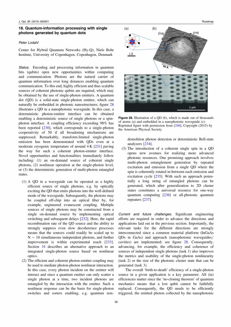
18. Quantum-information processing with singlephotons generated by quantum dots
Peter Lodahl
Center for Hybrid Quantum Networks (Hy-Q), Niels BohrInstitute, University of Copenhagen, Copenhagen, Denmark
Status. Encoding and processing information in quantumbits (qubits) open new opportunities within computingand communication. Photons are the natural carrier ofquantum information over long distances enabling quantumcommunication. To this end, highly efficient and thus scalablesources of coherent photonic qubits are required, which maybe obtained by the use of single-photon emitters. A quantumdot (QD) is a solid-state single-photon emitter, which cannaturally be embedded in photonic nanostructures; figure 28illustrates a QD in a nanophotonic waveguide. In this case, adeterministic photon-emitter interface can be obtainedenabling a deterministic source of single photons or a spin-photon interface. A coupling efficiency exceeding 98% hasbeen reported [230], which corresponds to a single-photoncooperativity of 50 if all broadening mechanisms aresuppressed. Remarkably, transform-limited single-photonemission has been demonstrated with QDs even at amoderate cryogenic temperature of around 4 K [231] pavingthe way for such a coherent photon-emitter interface.Novel opportunities and functionalities immediately followincluding: (1) an on-demand source of coherent singlephotons, (2) nonlinear operation at the single-photon level,or (3) the deterministic generation of multi-photon entangledstates.
(1) A QD in a waveguide can be operated as a highlyefficient source of single photons, e.g. by opticallyexciting the QD that emits photons into the well-definedmode of the waveguide. Subsequently, the photons maybe coupled off-chip into an optical fiber by, forexample, engineered evanescent coupling. Multiplesources of single photons may be constructed from asingle on-demand source by implementing opticalswitching and subsequent delays [232]. Here, the rapidrecombination rate of the QD source and the ability tostrongly suppress even slow decoherence processesmeans that the sources could readily be scaled up toN∼10 simultaneous independent photons, and furtherimprovement is within experimental reach [233].Section 34 describes an alternative approach to anintegrated single-photon source based on nonlinearoptics.
(2) The efficient and coherent photon-emitter coupling maybe used to mediate photon-photon nonlinear interaction.In this case, every photon incident on the emitter willinteract and since a quantum emitter can only scatter asingle photon at a time, two incident photons areentangled by the interaction with the emitter. Such anonlinear response can be the basis for single-photonswitches and sorters enabling, e.g. quantum non-
demolition photon detection or deterministic Bell-stateanalyzers [234].
(3) The introduction of a coherent single spin in a QDopens new avenues for realizing more advancedphotonic resources. One promising approach involvesmulti-photon entanglement generation by repeatedexcitation and emission from a single QD where thespin is coherently rotated in-between each emission andexcitation cycle [235]. With such an approach poten-tially a long string of entangled photons can begenerated, which after generalization to 2D clusterstates constitutes a universal resource for one-wayquantum computing [236] or all-photonic quantumrepeaters [237].
Current and future challenges. Significant engineeringefforts are required in order to advance the directions andapplications laid out in the previous section. Importantly, therelevant tasks for the different directions are stronglyinterconnected since a common material platform (InGaAsQDs in GaAs) and approach (nanophotonic waveguides/cavities) are implemented; see figure 28. Consequently,advancing, for example, the efficiency and coherence ofsources of independent single photons (task 1) also improvesthe metrics and usability of the single-photon nonlinearity(task 2) or the size of the photonic cluster state that can begenerated (task 3).
The overall ‘birth-to-death’ efficiency of a single-photonsource in a given application is a key parameter. All (in)efficiencies matter since the ‘no-cloning theorem’ of quantummechanics means that a lost qubit cannot be faithfullyreplaced. Consequently, the QD needs to be efficientlytriggered, the emitted photon collected by the nanophotonic
Figure 28. Illustration of a QD (b), which is made out of thousandsof atoms (a) and embedded in a nanophotonic waveguide (c).Reprinted figure with permission from [240], Copyright (2015) bythe American Physical Society.
39
J. Opt. 21 (2019) 063001 Roadmap

structure, the collected photon routed to the targeted photonapplication, the actual application must be low-loss, andeventually the photons must be detected with high efficiency.An important figure-of-merit characterizing the source is theprobability that an excitation of the QD leads to a photonpropagating in an optical fiber—the source efficiency. To thisend, resonant optical excitation on electrically-stabilized QDtransitions have been implemented and, for example, highly-efficient evanescent chip-to-fiber coupling structures havebeen designed. Combined with the ability to generate highlycoherent photons (the relevant figure-of-merit is the degree ofindistinguishability, which can exceed 95% [233]), this pavesthe way to a fiber-coupled deterministic source of photonicqubits. The efficiency and speed of optical switches and thepropagation loss in optical fiber delays will determine howthis source can be scaled up to generate many independentphotons on demand [233].
A highly-efficient nonlinearity operating at the level ofsingle photons is one of the missing functionalities inquantum photonics; see also section 35. The emitter-mediatednonlinear response constitutes a specific type of nonlinearity(‘a saturable emitter’) and current research uncovers how toexploit it. One example is that it allows us to implementdeterministic photon sorting, i.e. a superposition of one andtwo photons can be separated into the constituents. Thisenables constructing a resource efficient Bell state analyzer bythe use of only such a passive QD nonlinearity combined withspectral-temporal mode selection, linear optics, and photoncounting [238]. It is anticipated that many new (quantum andnon-quantum) applications will be developed exploiting thisnew paradigm of nonlinear optics.
The generation of advanced multi-photon entangledstates, such as photonic cluster states, is intimately relatedto the ability to prepare, coherently control, and maintain acoherent spin inside a QD embedded in a highly-efficientphotonic nanostructure. This is required in order to prepare ahigh-fidelity spin-photon entangled state, which is a pre-requisite for scaling up to multi-partite states. Very significantprogress is currently taking place in this research area wheretwo important efforts are to increase the spin coherence timeof the QD qubit and to enhance the radiative decay rate bothfor the benefit of generating multiple entangled photonsbefore decoherence sets in. The first founding proof-of-principle experiment has demonstrated entanglement betweentwo photons and a spin for a QD in a bulk sample [235].Implementing photonic nanostructures will allow scaling up.Next generation experiments will target the generation of 2Dclusters of entangled photons. This requires the ability toperform a two-qubit gate on the QD emitting photons, whichcould, for example, be obtained by introducing an additionalcoupled QD. The topology of the cluster state can be tailoredto a specific application. An example is the so-called ‘repeaterstates’ that may form the basis for an all-optical quantumrepeater where quantum entanglement can be remotelydistributed without the need for any quantum memory[239]. A specific proposal for how to use coupled QDs to
deterministically generate quantum repeater states was putforward recently [237] that seems feasible with the QDsystems presently available.
Advances in science and technology to meet challenges.Quantum communication is a relatively mature branch ofquantum technology comprising both technology already onthe market (e.g. trusted node quantum key distribution) andlong-term ultimate visions (e.g. a global ‘quantum internet’for remote entanglement generation and distribution).Importantly, quantum communication has the potential totap into and benefit from the already existing technology anddevelopments from the mature photonics industry. This alsoimplies that the new quantum technology would need tocomply with existing standards. The wavelength is one suchexample, and it will be essential to develop solutionsoperating in the telecom C-band (1.55 μm) in order tobenefit from the technology being developed for telecomindustry. Currently, the best performance of QDs has beenobtained in the near-infrared (900–1000 nm), and C-bandoperation could either be obtained by frequency conversion oralternatively would require improved growth of QDs tailoredto the C-band. The high demands on low-loss photoniccouplers, switches, and circuits, which are required forquantum applications, will push the boundaries of thepresent technology. Such developments could benefit fromand further advance ‘green ICT’ efforts and investmentsthat focus on developing energy-efficient informationand communication technology for classical opticalcommunication. Finally, a challenge pertains to scaling upany applications that requires multiple QDs, e.g. for theconstructing of a whole network of quantum repeater stations,since the inhomogeneities of each individual node wouldneed to be overcome either by local tuning of each quantumnode or by frequency-conversion tuning in-between thenodes.
Concluding remarks. The advancements in the control oflight–matter interaction with the use of QDs in nanophotonicstructures have matured to the level that a deterministicphoton-emitter interface is routinely generated. In the presentchapter, some of the potential applications of such a newquantum ‘building block’ in quantum-information processinghave been elaborated and engineering challenges have beenidentified.
Acknowledgments
I gratefully acknowledged financial support from the DanishNational Research Foundation (Center of Excellence ‘Hy-Q’),European Research Council (ERC Advanced Grant‘SCALE’), and Innovation Fund Dk (Quantum InnovationCenter ‘Qubiz’)
40
J. Opt. 21 (2019) 063001 Roadmap

19. Chip-based photon quantum state sources usingnonlinear optics
Xiang Zhang and Benjamin J Eggleton
University of Sydney, Sydney, Australia
Status. Quantum processing that utilizes the counterintuitiveproperties of quantum mechanics, such as superposition andentanglement, has opened the possibility for revolutionarytechnologies that will have a profound impact on our society,Examples of such disruptive technologies are quantumcomputing, secure communication system and quantumenhanced sensing [241, 242]. Although, different physicalsystems, such as superconducting circuits, trapped ion andelectron spin, have achieved major progress in recent yearsand are benefiting from significant industrial investments,photonic quantum technologies are going to play an essentialrole in the quantum revolution. These schemes are based onphotons—quanta of light—and have some intrinsicadvantages over other physical systems: (i) they provide anatural interface between quantum computing systems andlow-loss communication links; (ii) their coherence time islong enough for the logic gate control; and (iii) they arenearly free of environmental noise, namely thermal andelectromagnetic noise.
Over the last two decades, theoretical analysis andpreliminary demonstrations have established the supremacyof photonic quantum processing [243]. However, the majorchallenge for its practical application lies in the developmentof a highly reliable and large-scale photonic quantum system.Building such a system based on free-space opticalcomponents seems unviable due to its lack of robustness,stability and scalability. Integrated optics, on the other hand,allows for the harnessing of CMOS technology and henceachieves multi-scale integration of passive and activecomponents in a mature silicon-based platform that can bescaled up for manufacturing.
The ultimate goal of integrated quantum optics is toutilize the existing CMOS infrastructure to realize a fullyintegrated quantum photonic chip that contains high effi-ciency photon sources, low-loss and reconfigurable linearwaveguides and near-optimal single photon detectors. Manyof the core components of such a chip have already beendemonstrated in integration platforms, including low-losscircuits, tunable phase shifters and near-optimal detectors. Anon-chip photonic quantum state source that generates singleand entangled photons on-demand, however, is the ‘Achillesheel’ of this scheme. The on-chip photon source is the key tomove photonic quantum processing into the real world.
Current and future challenges. Two technical approaches arebeing pursued for building an on-chip single photon source.One is collecting single photons from a ‘single-emitter’embedded in the circuits (so called quantum dots). Althoughimpressive results have been obtained, the remaining barriersfor this scheme are indistinguishability of the single photonsfrom distinct sources and the lack of spectral flexibility. The
second approach is to directly generate single photons withinthe photonic circuits via nonlinear optical effects, such asspontaneous parametric down conversion (SPDC) orspontaneous four wave mixing (SFWM). Figures 29(a) and(b) show the schematic of SPDC and SFWM in LiNO3 andsilicon waveguides, respectively, and their underlyingprinciples are illustrated in figures 29(c) and (d). In thisnonlinear optics approach, the signal and idler photon aretime-correlated such that the detection of one photon heraldsthe existence of the other, hence it is referred to as a heraldedsingle photon source. Compared with the quantum dots, theheralded quantum light sources can generate highlyindistinguishable heralded single photons at roomtemperature and their frequency is tunable within abroadband spectrum. An intrinsic limitation of this scheme,however, is the low efficiency of the stochastic photongeneration.
To build a more deterministic single photon source,multiplexing (MUX) schemes that operate probabilisticprocesses in the spatial (SMUX) or time (TMUX) domainin parallel have been considered as a promising way forward[244, 245]. These schemes integrate the heralded singlephotons into a fixed mode by an active switching network asshown in figures 29(e) and (f). One major issue of thereported MUX schemes is the fast and ultra-low loss switch,which has not yet been demonstrated in an integratedplatform. The overall enhancement of the MUX schemes isdetermined by the losses of the switching network and themultiplexed mode number. The switching speed is anothercrucial point as it determines the saturation limit of MUX.The saturation margin can be further expanded by utilizing arelative multiplexing (RMUX) scheme which involves activesynchronization of N single photons instead of shifting eachphoton to a fixed temporal/spatial mode [246]. Beside MUX
Figure 29. On-chip heralded single photon source. (a) The schematicof SPDC in LiNO3 waveguide. (b) The schematic of SFWM insilicon waveguide. (c) Principle of SPDC. (d) Principle of SFWM.(e) SMUX. (f) TMUX.
41
J. Opt. 21 (2019) 063001 Roadmap

schemes, applying resonant structures will significantlyincrease the energy efficiency and spectral purity [247].
As another crucial component for integrated quantumphotonic, on-chip entanglement sources have been demon-strated in different integrated platforms, such as lithiumniobate, silicon, silicon nitride and hydex, as shown infigures 30(a)–(d), respectively [248–251]. The remainingchallenges for entangled photon sources include the genera-tion of multi-dimensional entanglement states with highfidelity and controlling these entanglement states with highprecision. Multi-dimensional entanglement states are verypromising resources for photonic quantum processing as theirdistinct quantum properties allow higher capacity, robustnessand error-tolerance. But it comes with the price of increaseddifficulties to generate and manipulate these states. Thegeneration efficiency of multi-dimensional entanglement stateexponentially decreases with the increasing dimension sincethe underlying nonlinear processes, e.g. SPDC and SFWM,are non-deterministic. Manipulating these high-dimensionalentanglement states without deteriorating their fidelity isanother challenge since each operation will affect the entirestate. A compact and reconfigurable integration platform is anelegant scheme to precisely control high-dimensional quant-um states; this was demonstrated for a 15×15 entanglementstate generated and controlled using in a fully integratedsilicon photonic chip, as shown in figures 30(e) and (f) [252].This work further confirms that integrated optics is promisingfor generating and manipulating high-dimensional entangle-ment states.
Advances in science and technology to meet challenges.Material engineering is one of the key approaches to developrobust and compact integration platforms with highnonlinearity and negligible linear and nonlinear loss over abroad bandwidth. Hybrid integration is one potential solutionto circumvent the aforementioned challenges by integratingdifferent materials and therefore different functions on onesingle platform, such as silicon photon source integrated withsilicon nitride/silica linear circuits.
Developing a resource efficient MUX will break theprobabilistic nature of heralded single photon sources. Recentdemonstration of frequency multiplexing (FMUX) shows apromising way to build a deterministic single photon source[253]. The advantage of FMUX over other MUX schemes isthat the losses are fixed irrespective of the mode number.However, a deterministic single photon wavelength conver-sion in integrated waveguides is a nontrivial task due to thedispersion control and linear/nonlinear loss.
In the future, a fully integrated photonic chip thatcontains electronic and photonic components could signifi-cantly simplify these systems. Integrating all these compo-nents on one chip, however, is not a straightforward task,even if each core component has been separately demon-strated in an integrated platform. One of the major obstacles isthat even though all components share the same environment,each device operates at different conditions, for instance,superconducting single photon detectors usually requirecryogenic temperature (2 K) to achieve near-unity detectionefficiency with negligible dark count noises. These ultra-lowtemperature impose a stringent requirement on the electronicdevice, such as the life-time of the switch driving circuits, theresponse time of the phase modulator and the latency insidethe control unit. In this circumstance, exploiting the electro-optic effect to achieve fast switching and phase tuning is key.
Concluding remarks. Although remarkable progress hasbeen achieved over the last decade, this field of on-chipphotonic quantum state source based on nonlinear opticsneeds continuous research efforts to achieve deterministicsingle photon generation and multi-dimensional entanglementstates with high fidelity, which will significantly boost thepractical development of photonic quantum processing.
Figure 30. On-chip entangled photon source. (a) LiNO3. (b) Silicon.(c) Si3N4. (d) Hydex. (e) High dimensional entanglement in a siliconchip. (f) Quantum state tomography results.
42
J. Opt. 21 (2019) 063001 Roadmap

20. Weak optical nonlinearities and their potential forefficient universal quantum computation
William John Munro1 and Kae Nemoto2
1NTT Basic Research Laboratories, Japan 2NationalInstitute of Informatics, Japan
Status. It is well known that optical quantum informationprocessing and especially computation requires photons tointeract with one another so that gates can be performed onthe information stored in those photons. The pioneering workof Knill, Laflamme and Milburn (KLM) [254] showed that, inprinciple, a universal set of quantum gates using polynomialresources could be performed using only linear opticalelements, single photon sources and detectors. The keydevelopment from this work was outlining how a two-qubitgate, the controlled NOT (CNOT) gate could be constructedin a probabilistic but heralded fashion and then teleportednear deterministically into the quantum circuit.
While this field is known as linear optical quantumcomputation, it does involve nonlinearities in both the sourcesand detectors. The fundamental question was whether wecould use a weak nonlinearity to construct a deterministicCNOT gate [255, 256]. We also already know (seefigure 31(a)) that weak nonlinearities can be used with anintense probe beam to indirectly measure the state of a qubit:a quantum non-demolition (QND) measurement. In this case,a weak cross-Kerr nonlinearity is used to write a differentialphase shift on the probe beam dependent on the state of thephotonic qubit as follows [257]:
H V H e V . 1ia a añ + ñ ñ ñ ñ + ñ ñq(∣ ∣ )∣ ∣ ∣ ∣ ∣ ( )
Then by measuring whether the probe beam is in the stateeia ñq∣ or añ∣ , one can make an indirect measurement of the
polarization state of the photon. The two resulting states ofthe probe beam are however not orthogonal with their overlapbeing given by
e e . 2i 2 4 sin 22 2a aá ñ = a qq -∣ ∣ ∣ ( )( )/
However, for sin 1a q these states are effectivelyorthogonal. With a weak nonlinearity 1,q we can use astronger probe field (larger a) to achieve 3aq ~ and soensure near orthogonally (errors <0.01% for instance [257]).The QND measurement thus benefits by being able to use aweak nonlinearity.
There is however no reason that we need to measure theprobe field after it interacts with the first photon in the weaknonlinearity. We could instead have it interact with a secondsingle photon in another weak nonlinearity [255, 256]. In thiscase, our resulting state is
H H e H V V H
V V e 31 2
i1 2 1 2
1 2i
a aa
ñ ñ ñ + ñ ñ + ñ ñ ñ
+ ñ ñ ñ
q
q-
∣ ∣ ∣ {∣ ∣ ∣ ∣ }∣∣ ∣ ∣ ( )
where we immediately note that the probe field associatedwith the even parity terms H H V V,1 2 1 2ñ ñ ñ ñ(∣ ∣ ∣ ∣ ) have pickedup phase shifts ( ,q q), respectively, while the probe fieldassociated with the odd parity terms H V V H,1 2 1 2ñ ñ ñ ñ(∣ ∣ ∣ ∣ ) picks
up no phase shift. Thus, measuring whether there has been aphase shift or not would thus perform an indirect paritymeasurement on the two polarization qubits. The issue is howto measure the probe field in such a way that we do not learnabout the sign of the component iq while maintaining the
3aq ~ constraint. Of course, there are a number of waysthis can be achieved but a natural one is to displace the probefield by D a-( ) using a strong laser field giving
H H V V H H V V
H V V H2 0
1 2 1 2 1 2 1 2
1 2 1 2
ñ ñ + ñ ñ +ñ + ñ ñ - ñ ñ - ñ
+ ñ ñ + ñ ñ ñ
(∣ ∣ ∣ ∣ )∣ (∣ ∣ ∣ ∣ )∣{∣ ∣ ∣ ∣ }∣
where i i .1
2aq aqñ = ñ - ñ∣ (∣ ∣ ) The ñ∣ probe states are
in fact Schrödinger cat states of even and odd photon numbersassuming 1.a Hence by measuring the photon numberof the probe beam we can project the polarization statesinto either H H V V ,1 2 1 2ñ ñ + ñ ñ∣ ∣ ∣ ∣ H H V V1 2 1 2ñ ñ - ñ ñ∣ ∣ ∣ ∣ orH V V H1 2 1 2ñ ñ + ñ ñ∣ ∣ ∣ ∣ depending on that result. The evenphoton number result also contains the 0∣ ⟩ componentassociated with the H V V H1 2 1 2ñ ñ + ñ ñ∣ ∣ ∣ ∣ state and so we againrequire e 4 sin 22 2a q- ( )/ ∼0 3aq ~( ) to ensure its contrib-ution is small. The constraint 3aq ~ means weaknonlinearities can be used as the mean photon number inthe probe field could be of order of a million or more.Nonlinear phase shifts of order of 0.28 radians have alreadybeen demonstrated [258]. For the odd photon number result,we apply a sign flip on one of the polarization qubits,transforming that state from H H V V1 2 1 2ñ ñ - ñ ñ∣ ∣ ∣ ∣ toH H V V .1 2 1 2ñ ñ + ñ ñ∣ ∣ ∣ ∣ The parity gate’s overall action meanswe can near deterministically distinguish even parity statesfrom odd [256].
While not the traditional CNOT gate, this parity gate issufficient with the other linear optical elements for universalquantum computation [259]. The parity gate is a morefundamental or primitive gate as a Bell state analyzer and
Figure 31. Schematic diagram of a quantum non-demolitionmeasurement (a) and parity gate (b). (a) The QND gate uses a weakcross phase modulation to impart a small phase shift on the probebeam for the Hñ∣ component of the polarization qubit. The phaseshift is then measured to determine the state of the qubit. The paritygate in (b) uses the setup for the QND measurement in (a) but insteadof measuring the probe, it transmits this probe field to a second QNDapparatus. The probe field is then displacement by an amount -α (byinputting the probe beam to a highly reflective beam splitter with astrong laser field on the second input port) and its photon numbermeasured.
43
J. Opt. 21 (2019) 063001 Roadmap

CNOT gate can be achieved using two such gates. Recenttheoretical developments have shown how the weak non-linearity approach can be used to construct more complicatedgates like the Fredkin, Toffoli and multi-controlled-unitarygates [260] as well as being useful for error correction anddetection operations both in computation and communication.In principle the parity gates could be distributed in nature andso used to entangle distant photons for quantum networks (seefigure 32) and even join separate cluster states together.
Current and future challenges. The original weak nonlinearityproposals were based on a single mode analysis. However, inpropagating situations, a multi-mode model for the input/outputfields is more appropriate—especially where it includes theinteraction with the nonlinear medium. The work by Shapiro andRazavi [261] showed in a non-instantaneous causal cross-Kerrmodel that phase noise is induced on the photonic fields givingthe possibility that the distributed parity gate may not be able toperform high fidelity nearly deterministic operations. They leftopen the possibility that different causal response functions thatmay work [261] and further raised the question of theapplicability of their model to atomic systems. More recentwork by Gea-Banacloche [262] considered a four-level atomoperating in the electromagnetically induced transparencyregime and showed that as long as the probability of photonabsorption in the atom is small, the maximum cross-phase-modulation is also limited. This supported the originalconclusions by Shapiro et al.
Advances in science and technology to meet challenges.The key challenge going forward is to determine in whatregimes the weak nonlinear cross-Kerr nonlinearity approachworks and for this the details of the physical system arecritical. One must really look closely at the properties of thesystems that generate the nonlinearities and its photonicsinteraction. There have been a number of recent developmentsin this aspect but two highlights are:
• First is a low-light-level cross-phase-modulation exper-imental demonstration by Chen et al [263]. It is based onthe light-storage technique in laser-cooled 87Rb atomsand they show a phase shift over 0.7 rad. A critical aspectof this work was the storage of the weak pulse in theatomic medium. While the focus of the experimentaleffort was on generating a π phase shift, there is potentialfor it to be applied to the weak nonlinearity approach.
• Second is a recent approach suggested by Kirby et al[264] where they suggest a method for producing a weakcross-phase modulation at the single-photon level usingmetastable xenon in a high finesse cavity. It has two mainadvantages. Firstly, the use of a high finesse cavity with a
single cavity resonant frequency existing within thebandwidth of the medium should avoid the freely-propagating beams issues raised previously. Secondly,the use of bulk xenon will simplify the experimentalimplementation as one does not need to trap single atoms.They predict that phase shifts of ∼20 milliradians shouldbe possible in this system. This small phase shift shouldbe useful for weak nonlinearity-based quantum gates.
Concluding remarks. Linear optical quantum computation,despite all of its impressive progress in recent years, suffersfrom the probabilistic nature of its entangling gates. Nonlinearenabled gates (whether they be based on strong cross phasemoderation, quantum zeno effects or weak nonlinearities)offer a solution to this issue with the potential for largephysical resource reductions. The weak nonlinearity approachis a potential bridge between the current linear and longer-term strong nonlinearity regimes. Incorporating nonlineargates in single photon circuits however needs to be done withextreme care. As has been pointed out by others, a detailedexamination is required including the overall system anddevice physics. Partial analysis built on idealized models maynot be what happens in the real system. Recently, Xia et al[265] have considered a cavity-free scheme for nondestructivesingle-photon detection where they pump a nonlinear mediumto implement an inter field Rabi oscillation. This leads to aphase shift on a probe field in the presence of a single signalphoton and presents a new way forward for the weak opticalnonlinearity approach.
Acknowledgments
We thank Jeff Shapiro, Jim Franson and Peter Knight forvaluable discussions on this weak nonlinearity approach. Thiswork was supported in part from a grant from the JohnTempleton Foundation (JTF #60478). The opinions expres-sed in this publication are those of the authors and do notnecessarily reflect the views of the John TempletonFoundation.
Figure 32. The parity gate can be used to create entangled betweenremote nodes in a quantum network which can be used for manypotential quantum tasks.
44
J. Opt. 21 (2019) 063001 Roadmap

21. Generation and amplification of opticalSchrödinger cats
Olivier Morin1 and Julien Laurat2
1Max-Planck-Institut für Quantenoptik, Garching, Germany2Laboratoire Kastler Brossel, Paris, France
Status. In parallel to single-photon generation andprocessing, a lot of effort has been dedicated over the last15 years to preparing an optical Schrödinger cat state. Thisstate of the form a añ - ñ∣ ∣ consists of a superposition ofcoherent states with opposite phase and mean photon number
.2a∣ ∣ Beyond their fundamental significance as an opticalversion of the Schrödinger’s thought experiment involvingthe superposition of macroscopically distinct components, catstates are also key resources for a variety of protocolsin quantum information processing, including quantummetrology, communication and computing [266, 267]. Inthe framework of linear optical quantum computing forinstance, coherent state quantum computing uses coherentstates as a qubit basis and fault-tolerant approaches andresource-efficient gates have been proposed [268].
More generally, this ongoing research enters into thecontext of engineering complex non-Gaussian states. Non-Gaussianity, which is related to negativities in the associatedWigner functions (figure 33(a)), is a general resource forquantum information science and technology and no-gotheorems prevent many quantum capabilities, if only based onGaussian states and operations [266]. The developedtoolboxes for preparation, manipulation and characterizationof optical cat states thereby contribute to this larger endeavorand the associated methods find applications in other physicalplatforms and regimes, such as in the microwave domain.
On the experimental front, a pioneering approach togenerate optical cat states relied on a probabilistic butheralded method [269]. By tapping a small fraction of asqueezed vacuum state, which is a Gaussian state generatedfor instance by parametric down conversion, and by detectinga single photon in this mode, a photon-subtraction operationis realized and turns the initial state into a free-propagating catstate (figure 33(b)). This state is usually called ‘kitten’because of the limited size 1.2a ~∣ ∣ The first experimentaldemonstration was achieved in 2006 and spurred an intenseexperimental and theoretical effort to engineer non-Gaussianstates.
Current and future challenges. The generation of opticalSchrödinger cat states remains challenging today. The purityof the state and fidelity to the targeted superposition are thefirst two important parameters. A strategy to build such statesoften requires some approximations, such as the size of theHilbert space. Optical losses that result from the generationitself or from the subsequent propagation are also majorissues, as no post-selection can be applied to these states thatlive in an intrinsically infinite-dimensional space. In any case,negativities of the Wigner function disappear after 50% loss.
A second central challenge is the size of the coherent-state superposition, i.e. the mean photon number .2a∣ ∣ Thissize is critical as it directly relates to the overlap between thetwo coherent states. For a value 2,2a =∣ ∣ the overlap is3.10−4. Depending on the application, the requirement can bedifferent. For computing tasks, the overlap should be limitedas it defines the orthogonality of the basis elements. Fault-tolerant schemes with moderate size 1.42a >∣ ∣ have beenproposed, albeit with a large resource overhead [268]. In otherapplications, e.g. quantum metrology, the large size is a keyfeature for potential enhancements.
Finally, the probabilistic approach, on which engineeringof such non-classical fields has been based so far, is a strongbottleneck as the preparation rate decreases drastically withthe size and with the number of cascaded operations. Thegeneration should be made deterministic and scalable forpratical use.
Ultimately, one wants to gather all of these features. Thisis extremely hard experimentally and most of the time one hasto define some tradeoff. Unfortunately, in contrast to singlephoton, there are no clear benchmarks on how good a cat statesource should be because of the multiple parameters involved.Fundamental investigations in this field will be important inthe future to better steer experimental efforts.
Figure 33. (a) Phase-space representation of a cat state with negativeWigner function. The state can be fully characterized via phase-sensitive homodyne detection. (b) Seminal technique for generatinga cat state by heralded photon subtraction applied to squeezed light.(c) Two cat states can be merged together to build a larger one. Thisbreeding operation requires on-demand sources, a current challengeof the field.
45
J. Opt. 21 (2019) 063001 Roadmap

Advances in science and technology to meet challenges.Optical loss is probably the most recurrent challenge inquantum state engineering and directly relates to the generalproblem of decoherence inherent to any realization inquantum physics. Technological progress, e.g. low-losscomponents, obviously helps to mitigate this problem, butthis is not the only option. It is also important to findstrategies where the impact of decoherence is minimized. Ithas been recently shown for instance that the negativity of theWigner function of a cat state can be made more robust tolosses by initially squeezing the superposition [270].Entanglement remotely prepared by some measurement-induced strategy can also overcome the loss in a channel,which then only affects the preparation rate and not the statefidelity. The recently demonstrated hybrid entanglementbetween particle-like and wave-like qubits enables in thisway the distant preparation of any cat state [271]. Thisongoing effort enters into the general context of the opticalhybrid approach to quantum information, which aims atcombining the traditionally separated discrete- andcontinuous-variable states, operations and tools to overcomesome individual limitiations or to provide novel capabilities[266, 267].
Increasing the size of the generated cat state, with2,2a >∣ ∣ is also a driving goal. Initial works were based on
two photon subtraction on squeezed light or homodyneconditioning on two-photon Fock states, albeit with lowgeneration rate. Very recent works have introduced novelstrategies. By building only the key non-Gaussian part of thetargeted state, one can generate a so-called core state that is agood approximation of the cat via only a Gaussian squeezingoperation [272]. This strategy minimizes the expensive non-Gaussian resource and enables it to reach higher size andmuch larger preparation rate. Squeezed cat states with
32a =∣ ∣ have been generated this way with a preparationrate above 200 Hz. Another method consists in increasing thesize by mixing a pair of cat states and producing a larger catby heralding [273, 274]. This ‘cat breeding’ operation can beextended in an iterative manner (figure 33(c)). The realizationof these new protocols can be facilitated, as experimentallyshown in [272], by the recent developments of high-efficiencysingle-photon detectors based on superconducting materials.Their remarkable progress towards a close-to-unity efficiencyis beginning to be a game changer, opening the realization ofprotocols that have been impossible so far.
However, all the aforementioned works are based onprobabilistic heralded protocols that fundamentally limit thescalability. On-demand generation is a crucial challenge, notonly for cat states. It has been particularly investigated in thecontext of single-photon generation to turn probabilisticheralded sources into quasi-deterministic ones. In this
context, recent works have provided some proof-of-conceptschemes by using either spatial multiplexing [275], whereseveral heralded sources are combined to a single outputmode using active switching, or buffer memories [276],where the heralded state is stored in an optical cavity andreleased when needed. This latter technique can be enhancedby time multiplexing. These strategies can be extended to thegeneration of cat states or any other non-Gaussian states, andwill be instrumental for the demonstration of iterativeprocesses where states need to be synchronized.
The common denominator of cat state generationmethods, as well as for Fock states, is their non-Gaussiancharacter. Fundamentally, such a feature requires optical non-linearities. In the case of the probabilistic techniques we havereviewed so far, the non-linearity is provided by the heraldingmeasurements, e.g. single-photon counting. However, adifferent approach could be used in order to generate thesestates deterministically, as it is now pursued with singlephotons. It is well known that non-linearities such as crossKerr effect for instance would enable the deterministicgeneration of cat states with arbitrary large size. To this endand also for many other applications like quantum gates, thedevelopment of systems exhibiting strong light–matterinteraction remains crucial. Their applications to non-Gaussian state engineering is still challenging as thesedevices need to exhibit very low loss. Novel generations ofcavity-QED systems, either bulk or at the nanoscale, as wellas ensembles of Rydberg atoms and emerging waveguide-QED devices with potential strong interaction in a single passwill certainly provide remarkable advances in the near future.Such cat-state generation will also be a strong benchmark oftheir performances.
Concluding remarks. A bit more than one decade after thefirst experimental demonstration, the field of optical cat stategeneration is very active, pushed by novel technologicalcapabilities and new promising schemes for enlarging them,protecting them better against decoherence and building themon-demand. Besides the specific example of coherent-statesuperpositions and their applications, harnessing complexnon-Gaussian states and exploring hybrid protocols aredriving goals of fundamental and practical importance.
Acknowledgments
The authors acknowledge the support from the EuropeanResearch Council (Starting Grant HybridNet), from SorbonneUniversité (PERSU program) and from the French NationalResearch Agency (Hy-Light project).
46
J. Opt. 21 (2019) 063001 Roadmap

22. Linear optical quantum computing
Josh Nunn
University of Bath, Bath, United Kingdom
Status. It is tempting to view quantum computing as thenext step in the exponential miniaturization enjoyed byclassical silicon processors. But in fact quantum computerswill solve certain high-value problems for industry andscience [277], and most likely will never be pocket-sized. Soin considering platforms for QIP, size does not matter, butscalability does: the ability to make a device more powerfulby adding more components. This is where linear optics mayoffer an advantage. The reason is that optical photons cancarry quantum information in ambient conditions, at roomtemperature. As there is no need to contain the processingcores in a vacuum system or a cryostat, there is a very lowbarrier to scaling, in terms of hardware. This contrasts withquantum platforms based on spin systems or microwavecavities, where the required high vacuum and refrigerationcould become infeasible, or at least impractical, at the scale of106 qubits. As photons are not charged, optical computation isimmune to fluctuating electrical and magnetic fields, soincreasingly large shielded environments are not needed.Furthermore, the ability to ‘wire up’ disparate parts of aphotonic processor with optical waveguides makesimplementing a high connectivity between qubitsstraightforward. Finally, the very high carrier frequency ofoptical photons (∼100 THz) means that this platform cansupport very high bandwidths, and can run at the fastestclock-rates permitted by electronic control logic (10 s ofGHz). But some difficulties remain.
In linear-optical QIP, qubits are encoded with individualphotons, and two-qubit gates—the key logical elements for aquantum computer—require the implementation of photon–photon entangling operations. Unfortunately for this purpose,the fact mentioned above that photons carry no charge meansthat they do not interact directly with one another. Photon–photon interactions mediated by electronic dipoles could beengineered, but the pursuit of deterministic two-photon gatesby this route represents a distinct approach to photonic QIP.The key feature of the ‘linear-optical’ approach is thatentangling operations are implemented by interference andmeasurement: the irreversible non-linear dynamics arisingfrom measurements in quantum mechanics replaces the directinteraction of photons [254]. The concomitant difficulty isthat measurement-induced entangling operations are funda-mentally probabilistic. This has so far prevented theimplementation of large-scale all-optical quantum processors.But, since the operations are based on measurements,successful operations can be heralded, meaning that althoughwe cannot predict when an entangling step will succeed, it ispossible to know as soon as it does. This provides a wayforward.
Current and future challenges. All modern proposals foruniversal quantum computing rely on the idea of topological
error correcting codes implemented on a very large entangledstate, within the paradigm of ‘one-way’ measurement-basedquantum computing [278]. The outstanding challenge inquantum optics is therefore the ability to build large entangledstates that cannot be efficiently simulated classically (inoptics, these are non-Gaussian entangled states). Rudolphet al have shown that probabilistic Type II fusion operations(equivalent to optical Bell measurements based on Hong-Ou-Mandel interference) can be used to grow large cluster states,given a resource of three-photon GHZ states [279]. Thus, thedevelopment of a deterministic source of GHZ entangledstates would be transformative. The creation of very largeGaussian entangled states has been demonstrated [280];similarly to the GHZ primitive mentioned above, on-demandimplementation of cubic phase gates [281] to de-Gaussifythese states would be transformative. However, as mentionedabove, linear-optics can deliver these states only non-deterministically. Therefore, scalability can only beachieved by multiplexing, which refers to the idea that aquasi-deterministic source can be engineered by combining alarge number of non-deterministic, heralded, sources. Tojustify this in broad terms, the probability that at least onesource out of N successfully produces a desired output isgiven by p1 1 ,N- -( ) where p is the success probability foreach source. Thus, what is needed is some large ensemble ofsources N p1 , / and an active element, for example aswitch, modulator or storage device, that is able to pick outthe successful event and route it into a fiducial mode thatserves as a quasi-deterministic output. To date, multiplexinghas been applied to the heralded generation of single photonsvia parametric scattering (photon pair-production by down-conversion and four-wave mixing) [282]. Fairly large GHZstates have been generated by unheralded pair sources in post-selection [283], and multiplexing has been applied to a rangeof Gaussian continuous-variable entangled states [284].However, thus far, the generation of heralded three photonGHZ states has not been achieved. This primitive requires thesimultaneous production of six single photons on-demand;once photonic multiplexing has reached sufficient maturity toenable it, the feasibility of full-scale linear-optical quantumcomputing will dramatically improve.
It is worth noting that all-optical simulations of vibronicspectra [285], molecular dynamics [286] and classical Isingoptimisations [287] have laid the groundwork for a suite ofnon-universal all-optical computers. But just as for universalquantum computing, multiplexed non-deterministic opera-tions are needed to access a regime that cannot be simulatedwith conventional computers.
Advances in science and technology to meet challenges.Multiplexing for scalability can be realized spatially,spectrally or temporally (see figures 34(b)–(d)). The first ofthese requires a large number of identical photon sources,interferometers and detectors, and the requisite componentdensity is best realized on-chip. Here, a fast, low-loss opticalswitch is needed to route the output of a successful operationinto a fiducial spatial mode. In spectral multiplexing, a single
47
J. Opt. 21 (2019) 063001 Roadmap

source can be operated over multiple frequency channelssimultaneously. In this case, a low-loss modulator or non-linear wave mixer is needed to shift desired outputs into afiducial spectral mode. Finally, in temporal multiplexing, asingle source is operated many times, and a quantum memory(a device for storing or buffering an optical pulse) must beincorporated in order to delay successful outputs and releasethem into a fiducial temporal mode. The key hardwareroadblock to the development of full-scale linear-opticalquantum computing has been the difficulty of engineeringsufficiently fast low-loss switches, modulators and memories.The requirements for loss and speed are linked becausemultiplexers must operate before waveguide propagationlosses become significant (‘significant’ being more than a fewpercent loss), which for on-chip architectures implies GHz-bandwidth switches are needed, and for fibre-based designs,∼10s of MHz bandwidth. This means that mechanical/piezo-electric, thermo-optical or acoustic switches are too slow.Electro-optical switching is fast enough but commerciallithium-niobate and opto-ceramic modulators are much toolossy. Pockels cells are efficient but bulky; Kerr-basedswitches are promising but the in- and out-coupling of
optical pump pulses presents a challenge where highefficiency and low noise are vital. Similar comments applyto spectral shifting, where serrodyne shifting with lithiumniobite modulators remains too lossy, and frequencytranslation by Bragg scattering four-wave mixing has a highinternal efficiency but is susceptible to Raman noise andleakage due to the need for intense optical pump pulses.Finally, quantum memories based on reversible absorption inatomic ensembles have separately achieved impressive figuresof merit for storage time, acceptance bandwidth, efficiencyand noise [288, 289]. Here, it is worth noting that a low-lossswitch (needed for spatial multiplexing) also enables quantummemory via switched cavities, and bulk electro-opticalimplementations offer arguably the best all-roundperformance [290], albeit they are too large to provide ascalable technology solution.
Concluding remarks. Quantum optics has a long pedigree inacademic laboratories, precisely because quantum effects areeasily accessible at room temperature, without the need forcryogenics, vacuum systems, advanced nanofabrication orextreme electromagnetic shielding. This gives a clue to thepotential scalability of linear optical quantum computing. Thetechnical difficulty of achieving fast, low-loss switching orquantum memory has so far put large scale all-optical QIP outof reach. But techniques to enable efficient multiplexing areemerging: once an on-demand source of heralded GHZentangled states (or an on-demand cubic phase gate) isdemonstrated, the possibility to build fault-tolerant universallinear-optical quantum computers becomes realistic.
Acknowledgments
The author acknowledges support from a Royal SocietyUniversity Research Fellowship and from the EPSRCQuantum Technology Hub NQIT.
Figure 34. In linear-optics quantum computing, measurement-basedheralded primitives must be multiplexed for scalability. (a) Theinterferometric scheme needed to produce a heralded three-photonGHZ state has not yet been demonstrated. Many such non-deterministic sources of entangled states must eventually becombined via (b) spatial, (c) spectral or (d) temporal multiplexing.
48
J. Opt. 21 (2019) 063001 Roadmap

ORCID iDs
Paolo Minzioni https://orcid.org/0000-0002-3087-8602Cosimo Lacava https://orcid.org/0000-0002-9950-8642Xiaoyong Hu https://orcid.org/0000-0002-1545-1491Ahmed Almaiman https://orcid.org/0000-0001-9526-8517Anna C Peacock https://orcid.org/0000-0002-1940-7172John E Bowers https://orcid.org/0000-0003-4270-8296Vibhav Bharadwaj https://orcid.org/0000-0002-7974-2597Benjamin J Eggleton https://orcid.org/0000-0003-4921-9727
References
[1] Tippett J T et al 1965 Optical and Electro-optical InformationProcessing (Cambridge, MA: MIT Press)
[2] Shamir J, John Caulfield H, Micelli W and Seymour R J 1986Optical computing and the Fredkin gates Appl. Opt. 25 1604–7
[3] O’Brien J L 2007 Optical quantum computing Science 3181567–71
[4] Shen Y, Harris N C, Scott S, Mihika P, Baehr-Jones T,Hochberg M and Soljacic M 2017 Deep learning withcoherent nanophotonic circuits Nat. Photon. 11 441–6
[5] Stegeman G I and Wright W M 1990 All-optical waveguideswitching Optical and Quant. Electron. 22 95–122
[6] Torruellas W E et al 1996 All‐optical switching by spatialwalkoff compensation and solitary‐wave locking Appl. Phys.Lett. 68 1449–51
[7] Durhuus T et al 1996 All-optical wavelength conversion bysemiconductor optical amplifiers J. Lightwave Technol. 14942–54
[8] Yoo S B 1996 Wavelength conversion technologies forWDM network applications J. Lightwave Technol. 14955–66
[9] He G S 2002 Optical phase conjugation: principles,techniques, and applications Prog. Quantum Electron. 26131–91
[10] Minzioni P 2009 Nonlinearity compensation in a fiber-optic linkby optical phase conjugation Fiber Integr. Opt. 28 179–209
[11] Leclerc O et al 2003 Optical regeneration at 40Gb/s andbeyond .J Lightwave Technol. 21 2779–90
[12] Blumenthal D et al 2003 Optical signal processing for opticalpacket switching networks IEEE Commun. Mag. 41 S23–9
[13] Blumenthal D et al 2000 All-optical label swapping networksand technologies J. Lightwave Technol. 18 2058
[14] Lacava C et al 2017 Nonlinear silicon photonic signalprocessing devices for future optical networks Appl. Sci. 7 103
[15] McKinstrie C J and Radic S 2004 Phase-sensitiveamplification in a fiber Opt. Express 12 4973–9
[16] Zhang Y, Husko C, Schröder J, Lefrancois S, Rey I H,Krauss T F and Eggleton B J 2014 Phase-sensitiveamplification in silicon photonic crystal waveguides Opt.Lett. 39 363–6
[17] Guan P, Røge K M, Lillieholm M, Galili M, Hu H,Morioka T and Oxenløwe L K 2017 Time lens based opticalfourier transformation for all-optical signal processing ofspectrally-efficient data J. Lightwave Technol. 35 799–806
[18] Zhang X et al 2016 Optical computing for optical coherencetomography Sci. Rep. 6 37286
[19] Malacarne A, Park Y, Li M, LaRochelle S and Azaña J 2015Real-time Fourier transformation of lightwave spectra andapplication in optical reflectometry Opt. Express 23 32516
[20] Martelli P et al 2009 All-optical wavelength conversion of a100-Gb/s polarization-multiplexed signal Opt. Express 1717758–63
[21] Da Ros F, Da Silva E P, Zibar D, Chu S T, Little B E,Morandotti R, Galili M, Moss D J and Oxenløwe L K 2018Optical wavelength conversion of high bandwidth phase-encoded signals in a high FOM 50 cm CMOS compatiblewaveguide arXiv preprint arXiv:
[22] Hausmann B J M et al 2014 Diamond nonlinear photonicsNat. Photon. 8 369
[23] Marhic M E et al 2014 Fiber optical parametric amplifiers inoptical communication systems Laser Photonics Rev. 950–74
[24] Wang D, Wu Z, Zhang M and Tang X 2018 Multifunctionalall-optical signal processing scheme for wavelength-division-multiplexing multicast, wavelength conversion,format conversion, and all-optical encryption using hybridmodulation format exclusive-OR gates based on four-wavemixing in highly nonlinear fiber Appl. Opt. 57 1562–8
[25] Lacava C et al 2017 Si-rich silicon nitride for nonlinear signalprocessing applications Sci. Rep. 7 22
[26] Aleksić S 2009 Analysis of power consumption in futurehigh-capacity network nodes J. Opt. Commun. Network. 1245–58
[27] Dunietz J 2017 Light-Powered Computers Brighten AI’sFuture (Scientific American)
[28] Miller S E, Marcatili E and Li T 1973 Research towardoptical-fiber transmission systems Proc. IEEE 61 1703–4
[29] Luo R, Jiang H, Rogers S, Liang H, He Y and Lin Q 2017On-chip second-harmonic generation and broadbandparametric down-conversion in a lithium niobatemicroresonator Opt. Express 25 24531–9
[30] Li Q, Davanço M and Srinivasan K 2016 Efficient and low-noise single-photon-level frequency conversion interfacesusing silicon nanophotonics Nat. Photon. 10 406
[31] Capmany J, Ortega B, Pastor D and Sales S 2005 Discrete-time optical processing of microwave signals J. LightwaveTechnol. 23 702–23
[32] Silver M, Manurkar P, Huang Y P, Langrock C, Fejer M M,Kumar P and Kanter G S 2017 Spectrally multiplexedupconversion detection with C-band pump and signalwavelengths IEEE Photon Tech Lett 29 1097–100
[33] Marchetti R et al 2017 High-efficiency grating-couplers:demonstration of a new design strategy Sci. Rep. 716670
[34] Marchetti R, Lacava C, Carroll L, Gradkowski K andMinzioni P 2018 Coupling strategies for silicon photonicsintegrated chips Photonics Res. 7 201–39
[35] Timurdogan E, Poulton C V, Byrd M J and Watts M R 2017Electric field-induced second-order nonlinear optical effectin silicon waveguides Nat. Photon. 11 200–6
[36] Cazzanelli M et al 2012 Second-harmonic generation insilicon waveguides strained by silicon nitride Nat. Mater. 11148–54
[37] Billat A, Grassani D, Pfeiffer M H P, Kharitonov S,Kippenberg T J and Brès C S 2017 Large second harmonicgeneration enhancement in Si3N4 waveguides by all-optically induced quasi-phase-matching Nat. Commun.8 1016
[38] Koos C et al 2009 All-optical high-speed signal processingwith silicon–organic hybrid slot waveguides Nat. Photon.3 216
[39] Guo X, Qiu M, Bao J, Wiley B J, Yang Q, Zhang X, Ma Y,Yu H and Tong L 2009 Direct coupling of plasmonic andphotonic nanowires for hybrid nanophotonic componentsand circuits Nano Lett. 9 4515–9
[40] Benson O 2011 Assembly of hybrid photonic architecturesfrom nanophotonic constituents Nature 480 193
49
J. Opt. 21 (2019) 063001 Roadmap

[41] McCall S L, Gibbs H M, Churchill G G andVenkatesan T N C 1975 Optical transistor and bistabilityBull. Amer. Phys. Soc. 20 636
[42] Tsuda H and Kurokawa T 1990 Construction of an all-opticalflip-flop by combination of two optical triodes Appl. Phys.Lett. 57 1724–6
[43] Hill M T, Dorren H J S, Vries T, Leijtens X J M, Besten J H,Smalbrugge B, Oei Y-S, Binsma H, Khoe G-D andSmit M K 2004 A fast low-power optical memory based oncoupled micro-ring lasers Nature 432 206–9
[44] Notomi M, Shinya A, Mitsugi S, Kira G, Kuramochi E andTanabe T 2005 Optical bistable switching action of Si high-Q photonic-crystal nanocavities Opt. Express 13 2678–87
[45] Tanabe T, Notomi M, Shinya A, Mitsugi S and Kuramochi E2005 Fast bistable all-optical switch and memory on siliconphotonic crystal on-chip Opt. Lett. 30 2575–7
[46] Soljačić M and Joannopoulous J D 2004 Enhancement ofnonlinear effect using photonic crystals Nat. Mater. 3 212–9
[47] Shinya A, Mitsugi S, Tanabe T, Notomi M, Yokohama I,Takara H and Kawanishi S 2006 All-optical flip-flop circuitcomposed of coupled two-port resonant tunneling filter intwo-dimensional photonic crystal slab Opt. Express 141230–5
[48] Kuramochi E, Nozaki K, Shinya A, Takeda K, Sato T,Matsuo S, Taniyama H, Sumikura H and Notomi M 2014Large-scale integration of wavelength-addressable all-optical memories on a photonic crystal chip Nat. Photonics 8474–81
[49] Ooka Y, Tetsumoto T, Fushimi A, Yoshiki W and Tanabe T2015 CMOS compatible high-Q photonic crystal nanocavityfabricated with photolithography on silicon photonicplatform Sci. Rep. 5 11312
[50] Fushimi A and Tanabe T 2014 All-optical logic gateoperating with single wavelength Opt. Express 22 4466–79
[51] Shoji Y, Shirato Y and Mizumoto T 2014 Silicon Mach–Zehnder interferometer optical isolator having 8nmbandwidth for over 20dB isolation Japan J. Appl. Phys. 53022202
[52] Keyes R W 1985 Optical logic-in the light of computertechnology Optica Acta: Int. J. Opt. 32 525–35
[53] Miller D A 2010 Are optical transistors the logical next step?Nat. Photon. 4 3
[54] Dong J, Zhang X and Huang D 2009 A proposal for two-inputarbitrary Boolean logic gates using single semiconductoroptical amplifier by picosecond pulse injection Opt. Express17 7725–30
[55] Liu Y, Tangdiongga E, Li Z, de Waardt H, Koonen A M J,Khoe G D, Shu X, Bennion I and Dorren H J S 2007 Error-free 320-Gb/s all-optical wavelength conversion using asingle semiconductor optical amplifier J. LightwaveTechnol. 25 103–8
[56] Dong J, Zhang X, Fu S, Xu J, Shum P and Huang D 2008Ultrafast all-optical signal processing based on singlesemiconductor optical amplifier and optical filtering J. Sel.Top. Quantum Electron. 14 770–8
[57] Huang D, Pintus P, Shoji Y, Morton P, Mizumoto T andBowers J E 2017 Integrated broadband Ce:YIG/Si Mach-Zehnder optical isolators with over 100 nm tuning rangeOpt. Lett. 42 4901–4
[58] Wang C and Li Z-Y 2013 Ultracompact linear on-chip siliconoptical logic gates with phase insensitivity Europhys. Lett.103 64001
[59] Lei L, Dong J, Yu Y, Tan S and Zhang X 2012 All-opticalcanonical logic units-based programmable logic array(CLUs-PLA) using semiconductor optical amplifiersJ. Lightwave Technol. 30 3532–9
[60] Nahmias M A, Shastri B J, Tait A N, Ferreira de Lima T andPrucnal P R 2018 Neuromorphic photonics Opt. PhotonicsNews 29 34–41
[61] Wang J, Yang J-Y, Huang H and Willner A E 2013 Three-input optical addition and subtraction of quaternary basenumbers Opt. Express 21 488–99
[62] Lattes A, Haus H, Leonberger F and Ippen E 1983 Anultrafast al-optical gate IEEE J. Quantum Electron. 191718–23
[63] Chen Y et al 2019 Nanoscale all-optical logic devices Sci.China Phys. Mech. Astron. 62 44201
[64] Piccione B, Cho C H, van Vugt L K and Agarwal R 2012 All-optical switching in individual semiconductor nanowiresNat. Nanotechnol. 7 640–5
[65] Wei H, Wang Z X, Tian X R, Kall M and Xu H X 2011Cascaded logic gates in nanophotonic plasmon networksNat. Commun. 2 387
[66] Wang F F, Hu X Y, Song H F, Li C, Yang H and Gong Q H2017 Ultralow-power all-optical logic date distributor basedon resonant excitation enhanced nonlinearity byupconversion radiative transfer Adv. Opt. Mater. 5 1700360
[67] Siozios A, Koutsogeorgis D C, Lidorikis E,Dimitrakopulos G P, Kehagias T, Zoubos H, Komninou P,Cranton W M, Kosmidis C and Patsalas P 2012 Opticalencoding by plasmon-based patterning: hard and inorganicmaterials become photosensitive Nano Lett. 12 259–63
[68] Ballarini D, Giorgi M D, Cancellieri E, Houdre R,Giacobino E, Cingolani R, Bramati A, Gigli G andSanvitto D 2013 All-optical polariton transistor Nat.Commun. 4 1778
[69] Saghatelian A, Völcker N H, Guckian K M, Lin V S-Y andGhadiri M R 2003 DNA-based photonic logic gates: AND,NAND, and INHIBIT J. Amer. Chem. Soc. 125 346–7
[70] Rosenberger J, Lin Q and Painter O 2009 Static and dynamicwavelength routing via the gradient optical force Nat.Photon. 3 478–83
[71] Sprague M R, Michelberger P S, Champion T F M,England D G, Nunn J, Jin X M, Kolthammer W S,Abdolvand A, Russell P S J and Walmsley I A 2014Broadband single-photon-level memory in a hollow-corephotonic crystal fibre Nat. Photon. 8 287–91
[72] Csaba G, Papp Á and Porod W 2017 Perspectives of usingspin waves for computing and signal processing Phys. Lett.A 381 1471–6
[73] Chumak A V, Vasyuchka V I, Serga A A and Hillebrands B2015 Magnon spintronics Nat. Phys. 11 453
[74] Papp Á, Porod W, Csurgay Á I and Csaba G 2017 Nanoscalespectrum analyzer based on spin-wave interference Sci. Rep.7 9245
[75] Gertz F, Kozhevnikov A V, Filimonov Y A,Nikonov D E and Khitun A 2015 Magnonic holographicmemory: from proposal to device IEEE J. Explor. Solid-State Comput. Devices Circuits 1 67–75
[76] Schneider T, Serga A A, Leven B, Hillebrands B,Stamps R L and Kostylev M P 2008 Realization of spin-wave logic gates Appl. Phys. Lett. 92 022505
[77] Maendl S, Stasinopoulos I and Grundler D 2017 Spin waveswith large decay length and few 100 nm wavelengths in thinyttrium iron garnet grown at the wafer scale Appl. Phys. Lett.111 012403
[78] Chumak A V, Serga A A and Hillebrands B 2014 Magnontransistor for all-magnon data processing Nat. Commun.5 4700
[79] Liu C, Chen J, Liu T, Heimbach F, Yu H, Xiao Y and Tu S2018 Long-distance propagation of short-wavelength spinwaves Nat. Commun. 9 738
[80] Egel E, Csaba G, Dietz A, Breitkreutz-von Gamm S, Russer J,Russer P and Becherer M 2018 Design of a 40-nm CMOSintegrated on-chip oscilloscope for 5–50 GHz spin wavecharacterization AIP Adv. 8 056001
[81] Csaba G, Papp A, Porod W and Yeniceri R 2015 Non-Boolean computing based on linear waves and oscillators
50
J. Opt. 21 (2019) 063001 Roadmap
Solid State Device Research Conf. (ESSDERC), 2015 45thEuropean pp 101–4(IEEE)
[82] Vahala K 2004 Optical Microcavities vol 5 (Singapore:World Scientific)
[83] Little B E et al 1999 Vertically coupled glass microringresonator channel dropping filters IEEE Photonics Technol.Lett. 11 215–7
[84] Van V et al 2002 Optical signal processing using nonlinearsemiconductor microring resonators IEEE J. Sel. Top.Quantum Electron. 8 705–13
[85] Heebner J E et al 2004 Optical transmission characteristics offiber ring resonators IEEE J. Quantum Electron. 40 726–30
[86] Goncharenko I A et al 2006 Optical broadband analog–digitalconversion on the base of microring resonator Opt.Commun. 257 54–61
[87] Yupapin P P and Suwancharoen W 2007 Chaotic signalgeneration and cancellation using a micro ring resonatorincorporating an optical add/drop multiplexer Opt.Commun. 280 343–50
[88] Ramachandran A et al 2008 A universal biosensing platformbased on optical micro-ring resonators Biosens. Bioelectron.23 939–44
[89] Ali J et al 2018 Coherent light squeezing states within amodified microring system Results in Physics 9 211–4
[90] Little B E et al 1998 Ultra-compact Si–SiO microringresonator optical channel dropping filters IEEE PhotonicsTechnol. Lett. 10 549–51
[91] Youplao P et al 2018 Plasmonic op-amp circuit model usingthe inline successive microring pumping techniqueMicrosyst. Technol. 24 3689–95
[92] Leclerc O, Lavigne B, Balmefrezol E, Brindel P, Pierre L,Rouvillain D and Seguineau F 2003 Optical regeneration at40Gb/s and beyond J. Lightwave Technol. 21 2779–90
[93] Agrell E et al 2016 Roadmap of optical communicationsJ. Opt. 18 063002
[94] Richardson D J, Fini J M and Nelson L E 2013 Space-division multiplexing in optical fibres Nat. Photonics 7354–62
[95] Sorokina M 2014 Design of multilevel amplitude regenerativesystem Opt. Lett. 39 2499–502
[96] Kakande J, Slavík R, Parmigiani F, Bogris A, Syvridis D,Grüner-Nielsen L, Phelan R, Petropoulos P andRichardson D J 2011 Multilevel quantization of opticalphase in a novel coherent parametric mixer architecture Nat.Photonics 5 748–52
[97] Guan P, Da Ros F, Lillieholm M, Kjøller N-K, Hu H,Røge K M, Galili M, Morioka T and Oxenløwe L K 2018Scalable WDM phase regeneration in a single phase-sensitive amplifier through optical time lenses Nat.Commun. 9 1049
[98] Buchali F 2004 Adaptive PMD compensation by electricaland optical techniques J. Lightwave Technol. 22 1116–26
[99] Cao Y et al 2016 Reconfigurable optical inter-channelinterference mitigation for spectrally overlapped QPSKsignals using nonlinear wave mixing in cascaded PPLNwaveguides Opt. Lett. 41 3233–6
[100] Ren Y et al 2014 Adaptive-optics-based simultaneous pre-and post-turbulence compensation of multiple orbital-angular-momentum beams in a bidirectional free-spaceoptical link Optica 1 376
[101] Almaiman A et al 2018 Phase-sensitive QPSK channel phasequantization by amplifying the fourth-harmonic idler usingcounter-propagating Brillouin amplification Opt. Commun.423 48–52
[102] Ettabib M A et al 2016 All-optical phase regenerationwith record PSA extinction ratio in a low-birefringencesilicon germanium waveguide J. Lightwave Technol. 343993–8
[103] Sun H, Wang K-Y and Foster A C 2017 Pump-degeneratephase-sensitive amplification in amorphous siliconwaveguides Opt. Lett. 42 3590–3
[104] Richardson D J, Fini J M and Nelson L E 2013 Space-division multiplexing in optical fibres Nat. Photon. 6 354–62
[105] Tong Z, Lundström C, Andrekson P A, McKinstrie C J,Karlsson M, Blessing D J, Tipsuwannakul E, Puttnam B J,Toda H and Grüner-Nielsen L 2011 Towards ultrasensitiveoptical links enabled by low-noise phase-sensitive amplifiersNat. Photon. 5 430–6
[106] Slavík R et al 2010 All-optical phase and amplituderegenerator for next-generation telecommunications systemsNature Photon. 4 690–5
[107] Olsson S L I, Corcoran B, Lundström C, Eriksson T A,Karlsson M and Andrekson P A 2015 Phase-sensitiveamplified transmission links for improved sensitivity andnonlinearity tolerance J. Lightwave Technol. 33 710–21
[108] Ji X, Barbosa F A S, Roberts S P, Dutt A, Cardenas J,Okawachi Y, Bryant A, Gaeta A L and Lipson M 2017Ultra-low-loss on-chip resonators with sub-milliwattparametric oscillation threshold Optica 4 619–24
[109] Ooi K J A, Ng D K T, Wang T, Chee A K L, Ng S K,Wang Q, Ang L K, Agarwal A M, Kimerling L C andTan D T H 2017 Pushing the limits of CMOS opticalparametric amplifiers with USRN:Si7N3above the two-photon absorption edge Nat. Commun. 8 13878
[110] Da Ros F, Vukovic D, Gajda A, Dalgaard K, Zimmermann L,Tillack B, Galili M, Petermann K and Peucheret C 2014Phase regeneration of DPSK signals in a silicon waveguidewith reverse-biased p-i-n junction Opt. Express 22 5029–36
[111] Pu M, Ottaviano L, Semenova E and Yvind K 2016 Efficientfrequency comb generation in AlGaAs-on-insulator Optica 3823–6
[112] Neo R, Schröder J, Paquot Y, Choi D-Y, Madden S,Luther-Davies B and Eggleton B J 2013 Phase-sensitiveamplification of light in a χ(3) photonic chip using adispersion engineered chalcogenide ridge waveguide Opt.Express 21 7926
[113] Liu X, Pu M, Zhou B, Krückel C J, Fülöp A,Torres-Company V and Bache M 2016 Octave-spanningsupercontinuum generation in a silicon-rich nitridewaveguide Opt. Lett. 41 2719–22
[114] Ballato J and Dragic P 2016 Glass: the carrier of light—abrief history of optical fiber Int. J. Appl. Glass Sci. 7 413–22
[115] Peacock A C, Sparks J R and Healy N 2014 Semiconductoroptical fibres: progress and opportunities Laser Photon. Rev.8 53–72
[116] Pöllinger M and Rauschenbeutel A 2010 All-optical signalprocessing at ultra-low powers in bottle microresonatorsusing the Kerr effect Opt. Express 18 17764–75
[117] Vukovic N, Healy N, Suhailin F H, Mehta P, Day T D,Badding J V and Peacock A C 2013 Ultrafast optical controlusing the Kerr nonlinearity in hydrogenated amorphoussilicon microcylindrical resonators Sci. Rep. 3 2885
[118] Shen L, Healy N, Xu L, Cheng H Y, Day T D, Price J H V,Badding J V and Peacock A C 2014 Four-wave mixing andoctave-spanning supercontinuum generation in a small corehydrogenated amorphous silicon fiber pumped in the mid-infrared Opt. Lett. 39 5721–4
[119] Healy N, Fokine M, Franz Y, Hawkins T, Jones M, Ballato J,Peacock A C and Gibson U J 2016 CO2 laser‐induceddirectional recrystallization to produce single crystal silicon‐core optical fibers with low loss Adv. Opt. Mater. 4 1004–8
[120] Kopp C, Bernabé S, Ben Bakir B, Fedeli J M, Orobtchouk R,Schrank F, Porte H, Zimmermann L and Tekin T 2011Silicon photonic circuits: on-CMOS integration, fiber opticalcoupling, and packaging IEEE J. Sel. Top. QuantumElectron. 17 498–509
51
J. Opt. 21 (2019) 063001 Roadmap

[121] Ren H, Aktas O, Franz Y, Runge A F J, Hawkins T, Ballato J,Gibson U J and Peacock A C 2017 Tapered silicon corefibers with nano-spikes for optical coupling via spliced silicafibers Opt. Express 25 24157–63
[122] Healy N, Mailis S, Bulgakova N M, Sazio P J A, Day T D,Sparks J R, Cheng H Y, Badding J V and Peacock A C 2014Extreme electronic bandgap modification in laser-crystallized silicon optical fibres Nat. Mater. 13 1122–7
[123] Suhailin F H, Shen L, Healy N, Xiao L, Jones M, Hawkins M,Ballato J, Gibson U J and Peacock A C 2016 Taperedpolysilicon core fibers for nonlinear photonics Opt. Lett. 411360–3
[124] Burla M, Cortés L R, Li M, Wang X, Chrostowski L andAzaña J 2013 Integrated waveguide Bragg gratings formicrowave photonics signal processing Opt. Express 2125120–47
[125] Mak J C C, Sacher W D, Xue T, Mikkelsen J C, Yong Z andPoon J K S 2015 Automatic resonance alignment of high-order microring filters IEEE J. Quantum Electron. 510600411
[126] Liang D, Huang X, Kurczveil G, Fiorentino M andBeausoleil R G 2016 Integrated finely tunable microringlaser on silicon Nat. Photonics 10 719–22
[127] Hendrickson S M, Foster A C, Camacho R M and Clader B D2014 Integrated nonlinear photonics: emerging applicationsand ongoing challenges [invited] J. Opt. Soc. Am. B 31 3193
[128] Harris N C, Grassani D, Simbula A, Pant M, Galli M,Baehr-Jones T, Hochberg M, Englund D, Bajoni D andGalland C 2014 Integrated source of spectrally filteredcorrelated photons for large-scale quantum photonic systemsPhys. Rev. X 4 41047
[129] Grillanda S, Carminati M, Morichetti F, Ciccarella P,Annoni A, Ferrari G, Strain M, Sorel M, Sampietro M andMelloni A 2014 Non-invasive monitoring and control insilicon photonics using CMOS integrated electronics Optica1 129–36
[130] Pasquazi A et al 2013 Self-locked optical parametricoscillation in a CMOS compatible microring resonator: aroute to robust optical frequency comb generation on a chipOpt. Express 21 13333
[131] Strain M J, Lacava C, Merrigi L, Cristiani I and Sorel M 2014Tunable Q-factor silicon micro-ring resonators for ultra-lowpower parametric processes Opt. Lett. 40 1274–7
[132] Chen L, Xu Q, Wood M and Reano R 2014 Hybrid siliconand lithium niobate electro-optical ring modulator Optica 1112–8
[133] Corbett B, Loi R, Zhou W, Liu D and Ma Z 2017 Transferprint techniques for heterogeneous integration of photoniccomponents Prog. Quantum Electron. 52 1–17
[134] McPhillimy J, Guilhabert B, Klitis C, Dawson M D,Sorel M and Strain M J 2018 High accuracy transfer printingof single-mode membrane silicon photonic devices Opt.Express 26 297–300
[135] Zhang J, Haq B, Callaghan J O, Pelucchi E, Trindade A J,Morthier G and Roelkens G 2018 Transfer-printing-basedintegration of a III–V-on-silicon distributed feedback laserOpt. Express 26 875–8
[136] Guilhabert B G, McPhillimy J, May S, Klitis C,Dawson M D, Sorel M and Strain M J 2018 Hybridintegration of an evanescently coupled AlGaAs microdiskresonator with a silicon waveguide by nanoscale-accuracytransfer printing Opt. Lett. 43 4883–6
[137] Richardson D J, Fini J M and Nelson L E 2013 Space divisionmultiplexing in optical fibers Nat. Photon. 7 354–62
[138] Demas J et al 2017 High-power, wavelength-tunable NIR all-fiberlasers via intermodal four-wave mixing JTh5A.8, CLEO US
[139] Demas J, Steinvurzel P, Tai B, Rishoj L, Chen Y andRamachandran S 2015 Intermodal nonlinear mixing withBessel beams in optical fiber Optica 2 14–7
[140] Bendahmane A, Krupa K, Tonello A, Modotto D,Sylvestre T, Couderc V, Wabnitz S and Millot G 2018Seeded intermodal four-wave mixing in a highly multimodefiber J. Opt. Soc. Am. B 35 295–301
[141] Lopez-Galmiche G, Sanjabi Eznaveh Z, Eftekhar M A,Antonio Lopez J, Wright L G, Wise F,Christodoulides D and Amezcua Correa R 2016 Visiblesupercontinuum generation in a graded index multimodefiber pumped at 1064 nm Opt. Lett. 41 2553–6
[142] Liu Z, Wright L G, Christodoulides D N and Wise F W 2016Kerr self cleaning of femtosecond-pulsed beams in graded-index multimode fiber Opt. Lett. 41 3675–8
[143] Wright L G, Renninger W H, Christodoulides D N andWise F W 2015 Spatiotemporal dynamics of multimodeoptical solitons Opt. Express 23 3492–506
[144] Nazemosadat E, Pourbeyram H and Mafi A 2016 Phasematching for spontaneous frequency conversion via four-wave mixing in graded-index multimode optical fibersJ. Opt. Soc. Am. B 33 144–50
[145] Friis S M M, Begleris I, Jung Y, Rottwitt K, Petropoulos P,Richardson D J, Horak P and Parmigiani F 2016 Inter-modalfour-wave mixing study in a two-mode fiber Opt. Express 2430338–49
[146] Parmigiani F, Horak P, Jung Y, Grüner-Nielsen L, Geisler T,Petropoulos P and Richardson D J 2017 All-optical modeand wavelength converter based on parametric processes in athree-mode fiber Opt. Express 25 33602–9
[147] Esmaeelpour M, Essiambre R-J, Fontaine N K, Ryf R,Toulouse J, Sun Y and Lingle R 2017 Power fluctuations ofintermodal four-wave mixing in few-mode fibersJ. Lightwave Technol. 35 2429–35
[148] Ellis A D, Patrick D M, Flannery D, Manning R J,Davies D A O and Spirit D M 1995 Ultra-high-speed OTDMnetworks using semiconductor amplifier-based processingnodes J. Lightwave Technol. 13 761–70
[149] Ohtsuki T and Matsuura M 2018 Wavelength conversion of25-Gbit/s PAM-4 signals using a quantum-Dot SOAPhoton. Technol. Lett. 30 459–62
[150] Hajomer A A, Yang X, Hu W, Andriolli N, Presi M,Porzi C and Contestabile G 2018 All-optical wavelengthconversion of PAM-4 signal using photonic integratedturbo-switch Asia Communications and Photonics Conf.ACP2018 p S3K.6(Hangzhou, China)
[151] Filion B, Jiachuan L, Nguyen A T, Zhang X,LaRochelle S and Rusch L A 2016 Semiconductor opticalamplifier-based wavelength conversion of nyquist-16QAMfor flex-grid optical networks J. Lightwave Technol. 342724–9
[152] Naimi S T, Duill S P Ó and Barry L P 2015 All opticalwavelength conversion of nyquist-WDM superchannelsusing FWM in SOAs J. Lightwave Technol. 33 3959–67
[153] Contestabile G, Maruta A and Kitayama K 2010 Gaindynamics in quantum dot semiconductor optical amplifiersat 1550 nm Photon. Technol. Lett. 22 987–9
[154] Akiyama T, Sugawara M and Arakawa Y 2007 Quantum-dot semiconductor optical amplifiers Proc. IEEE 951757–66
[155] Contestabile G, Maruta A, Sekiguchi S, Morito K,Sugawara M and Kitayama K 2010 Regenerativeamplification by using self phase modulation in a quantumdot SOA Photon. Technol. Lett. 22 492–4
[156] Contestabile G, Yoshida Y, Maruta A and Kitayama K 2012Ultra-broad band, low power, highly efficient coherentwavelength conversion in quantum dot SOA Opt. Express20 27902–7
[157] Ratovelomanana F et al 1995 An all-optical wavelength-converter with semiconductor optical amplifiersmonolithically integrated in an asymmetric passive Mach-Zehnder interferometer Photon. Technol. Lett. 7 992–4
52
J. Opt. 21 (2019) 063001 Roadmap

[158] Andriolli N, Faralli S, Bontempi F and Contestabile G 2013 Awavelength-preserving photonic integrated regenerator forNRZ and RZ signals Opt. Express 21 20649–55
[159] Nicholes S C, Masanovic M L, Jevremovic B, Lively E,Coldren L A and Blumenthal D J 2010 An 8 × 8 InPmonolithic tunable optical router (MOTOR) packetforwarding chip J. Lightwave Technol. 28 641–50
[160] Capmany J and Novak D 2007 Microwave photonicscombines two worlds Nat. Photonics 1 319
[161] Lim C, Nirmalathas A, Bakaul M, Gamage P, Lee K, Yang Y,Novak D and Waterhouse R 2010 Fiber-wireless networks andsubsystem technologies J. Lightwave Technol. 28 390–405
[162] Yao J 2009 Microwave photonics J. Lightwave Technol. 27314–35
[163] Ghelfi P et al 2014 A fully photonics-based coherent radarsystem Nature 507 341–5
[164] Marpaung D, Roeloffzen C, Heideman R, Leinse A,Sales S and Capmany J 2013 Integrated microwavephotonics Laser Photon. Rev. 7 506–38
[165] Hoessbacher C et al 2017 Plasmonic modulator with>170 GHz bandwidth demonstrated at 100 GBd NRZ Opt.Express 25 1762–8
[166] Liang W, Eliyahu D, Ilchenko V, Savchenkov A, Matsko A,Seidel D and Maleki L 2015 High spectral purity Kerrfrequency comb radio frequency photonic oscillator Nat.Commun. 6 7957
[167] Marpaung D, Morrison B, Pagani M, Choi D,Luther-Davies B, Madden S and Eggleton B 2015 Lowpower, chip-based stimulated Brillouin scattering microwavephotonic filter with ultrahigh selectivity Optica 2 76–83
[168] Pérez D et al 2017 Multipurpose silicon photonics signalprocessor core Nat. Commun. 8 636
[169] Liu Y, Hotten J, Choudhary A, Eggleton B and Marpaung D2017 All-optimized integrated RF photonic notch filter Opt.Lett. 42 4631
[170] Singh A et al 2015 Jupiter rising: a decade of Clos topologiesand centralized control in Google’s datacenter network Proc.2015 ACM Conf. on Special Interest Group on DataCommunication pp 183–97
[171] CISCO 2018 Cisco Global Cloud Index Forecast andMethodology, 2016–2021
[172] IEEE 802.3bs 200G and 400Gb/s Ethernet Task Force(http://ieee802.org/3/bs/public/index.html)
[173] Eiselt N, Wei J, Griesser H, Dochhan A, Eiselt M H,Elbers J-P, Olmos J J V and Monroy I T 2017 Evaluation ofreal-time 8×56.25Gb/s (400G) PAM-4 for inter-datacenter application over 80km of SSMF at 1550nmJ. Lightwave Technol. 35 955–62
[174] Le T S, Schuh K, Chagnon M, Buchali F, Dischler R, Aref V,Buelow H and Engenhardt K M 2018 1.72-Tb/s virtual-carrier-assisted direct-detection transmission over 200km JLightwave Technol. 36 1347–53
[175] Liu Z, Xu T, Saavedra G and Bayvel P 2018 448-Gb/s PAM4transmission over 300-km SMF-28 without dispersioncompensation fiber OFC W1J.6
[176] Markov I L 2014 Limits on fundamental limits tocomputation Nature 512 147–54
[177] Saleh A A M 2013 Evolution of the architecture andtechnology of data centers towards exascale and beyondOFC OM2D.4
[178] Filer M, Searcy S, Fu Y, Nagarajan R and Tibuleac S 2017Demonstration and performance analysis of 4 Tb/s DWDMmetro-DCI system with 100 G PAM4 QSFP28 modulesOFC W4D.4
[179] Perin J K, Shastri A and Kahn J M 2017 Design of low-powerDSP-free coherent receivers for data center J. LightwaveTechnol. 35 4650–62
[180] García López I et al 2017 DAC-free ultralow-power dual-polarization 64-QAM transmission at 32GBd with hybrid
InP IQ SEMZM and BiCMOS drivers module J. LightwaveTechnol. 35 404–10
[181] Liu Z, Kakande J, Kelly B, O’Carroll J, Phelan R,Richardson D and Slavík R 2014 Modulator-free quadratureamplitude modulation signal synthesis Nat. Commun. 5 5911
[182] Verbist J et al 2018 DAC-less and DSP-free 112Gb/s PAM-4transmitter using two parallel electroabsorption modulatorsJ. Lightwave Technol. 36 1281–6
[183] Lowery A J, Zhuang L, Corcoran B, Zhu C and Xie Y 2017Photonic circuit topologies for optical OFDM and nyquistWDM J. Lightwave Technol. 35 781–91
[184] Doerr C R, Chandrasekhar S, Winzer P J, Chraplyvy A R,Gnauck A H, Stulz L W, Pafchek R and Burrows E 2004Simple multichannel optical equalizer mitigatingintersymbol interference for 40-Gb/s nonreturn-to-zerosignals J. Lightwave Technol. 22 249–56
[185] Liu Z, Kim J Y, Wu D S, Richardson D J and Slavik R 2015Homodyne OFDM with optical injection locking for carrierrecovery J. Lightwave Technol. 33 34–41
[186] Mazur M, Lorences-Riesgo A, Schroeder J, Andrekson P andKarlsson M 2018 10 Tb/s PM-64QAM self-homodynecomb-based superchannel transmission with 4% shared pilottone overhead J. Lightwave Technol. 36 3176–84
[187] Blumenthal D et al 2011 Integrated photonics for low-powerpacket networking IEEE J. Sel. Top. Quantum Electron. 17458–71
[188] Kim J, Cox J A, Chen J and Kärtner F X 2008 Drift-freefemtosecond timing synchronization of remote optical andmicrowave sources Nat. Photon. 2 733–6
[189] Komljenovic T et al 2015 Heterogeneous silicon photonicintegrated circuits J. Lightwave Technol. 34 20–35
[190] Spencer D T et al 2018 An optical-frequency synthesizerusing integrated photonics Nature 557 81–5
[191] Chang L et al 2018 Heterogeneously integrated GaAswaveguides on insulator for efficient frequency conversionLaser Photon. Rev. 12 1800149
[192] Wang C et al 2018 Ultrahigh-efficiency wavelengthconversion in nanophotonic periodically poled lithiumniobate waveguides Optica 5 1438
[193] Chang L et al 2017 Heterogeneous integration of lithiumniobate and silicon nitride waveguides for wafer-scalephotonic integrated circuits on silicon Opt. Lett. 42 803
[194] Rao A et al 2016 Second-harmonic generation inperiodically-poled thin film lithium niobate wafer-bonded onsilicon Opt. Express 24 29941
[195] Pu M et al 2018 Ultra-efficient and broadband nonlinearAlGaAs-on-insulator chip for low-power optical signalprocessing Laser Photon. Rev. 12 1800111
[196] Davenport M L, Chang L, Huang D, Volet N and Bowers J E2016 Heterogeneous photonic integration by direct waferbonding ECS Trans. 75 179–83
[197] Hahn H et al 2018 Gallium phosphide-on-silicon dioxidephotonic devices J. Lightwave Technol. 36 2994–3002
[198] Chang L, Li Y, Volet N, Wang L, Peters J and Bowers J E2016 Thin film wavelength converters for photonicintegrated circuits Optica 3 531
[199] Zhang M et al 2017 Monolithic ultra-high-Q lithium niobatemicroring resonator Optica 4 1536
[200] Guha B et al 2017 Surface-enhanced gallium arsenide photonicresonator with quality factor of 6×10⁶ Optica 4 218
[201] Chang L et al 2018 Strong frequency conversion inheterogeneously integrated GaAs resonators IEEE PhotonicsConf. (IPC) Postdeadline
[202] Boes A, Corcoran B, Chang L, Bowers J and Mitchell A 2018Status and potential of lithium niobate on insulator (LNOI) forphotonic integrated circuits Laser Photonics Rev. 12 1–19
[203] Weigel P O et al 2016 Lightwave circuits in lithium niobatethrough hybrid waveguides with silicon photonics Sci. Rep.6 22301
53
J. Opt. 21 (2019) 063001 Roadmap

[204] Ellis A D et al 2016 4 Tb/s transmission reach enhancementusing 10×400 Gb/s super-channels and polarizationinsensitive dual band optical phase conjugation J. LightwaveTechnol. 34 1717–23
[205] Klonidis D et al 2014 Enabling transparent technologies forthe development of highly granular flexible optical cross-connects Int. Conf. on Transparent Optical Networks(ICTON)
[206] Pincemin E et al 2014 Multi-band OFDM transmission at100 Gbps with sub-band optical switching J. LightwaveTechnol. 32 2202–19
[207] da Silva E P et al 2016 Combined optical and electricalspectrum shaping for high-baud-rate nyquist-WDMtransceivers IEEE Photonics J. 8 1–11
[208] Ibrahim S K et al 2010 Towards a practical implementation ofcoherent wdm: analytical, numerical, and experimentalstudies IEEE Photonics J. 2 833–47 in
[209] Hu J et al 2018 Flexible width nyquist pulse based on a singleMach-Zehnder modulator Conf. on Lasers and Electro-Optics (CLEO) p SF3N.6
[210] Fabbri S J et al 2012 Multi-harmonic optical comb generationEuropean Conf. and Exhibition on OpticalCommunications (ECOC)
[211] Zhuang L et al 2016 Nyquist-filtering (de)multiplexer using aring resonator assisted interferometer circuit J. LightwaveTechnol. 34 1732–8
[212] Brès C S et al 2010 Optical demultiplexing of 320 Gb/s to8×40 Gb/s in single parametric gate J. LightwaveTechnol. 28 434–42
[213] Fabbri S J et al 2015 Experimental implementation of an all-optical interferometric drop, add, and extract multiplexer forsuperchannels J. Lightwave Technol. 33 1351–7
[214] Prawer S and Greentree A D 2008 Diamond for quantumcomputing Science 320 1601–2
[215] Childress L and Hanson R 2013 Diamond NV centers forquantum computing and quantum networks MRS Bull. 38134–8
[216] Hensen B et al 2015 Loophole-free Bell inequality violationusing electron spins separated by 1.3 kilometres Nature 526682–6
[217] Dolde F, Jakobi I, Naydenov B, Zhao N, Pezzagna S,Trautmann C, Meijer J, Neumann P, Jelezko F andWrachtrup J 2013 Room-temperature entanglement betweensingle defect spins in diamond Nat. Phys. 9 139–43
[218] Castelletto S et al 2011 Diamond-based structures to collectand guide light New J. Phys. 13 025020
[219] Pezzagna S, Naydenov B, Jelezko F, Wrachtrup J andMeijer J 2010 Creation efficiency of nitrogen vacancycentres in diamond New J. Phys. 12 065017
[220] Rondin L, Tetienne J-P, Hingant T, Roch J F,Maletinsky P and Jacques V 2014 Magnetometry withnitrogen-vacancy defects in diamond Rep. Prog. Phys. 77056503
[221] Wrachtrup J and Jelezko F 2006 Processing quantuminformation in diamond J. Phys.: Condens. Matter 18 S807
[222] Osellame R, Cerullo G and Ramponi R 2012 FemtosecondLaser Micromachining (Springer) vol 123
[223] Simmonds R D, Salter P S, Jesacher A and Booth M J 2011Three dimensional laser microfabrication in diamond using adual adaptive optics system Opt. Express 19 24122–8
[224] Sotillo B et al 2016 Diamond photonics platform enabled byfemtosecond laser writing Sci. Rep. 6 35566
[225] Bharadwaj V, Courvoisier A, Fernandez T T, Ramponi R,Galzerano G, Nunn J, Booth M J, Osellame R,Eaton S M and Salter P S 2017 Femtosecond laserinscription of Bragg grating waveguides in bulk diamondOpt. Lett. 42 3451–3
[226] Chen Y C et al 2017 Laser writing of coherent colour centresin diamond Nat. Photon. 11 77–80
[227] Sotillo B et al 2017 Visible to infrared diamond photonicsenabled by focused femtosecond laser pulsesMicromachines 8 60
[228] Chen Y C et al 2018 Laser writing of individual atomicdefects in a crystal with near-unity yield arXiv:1807.04028
[229] Hadden J P et al 2017 Integrated waveguides anddeterministically positioned nitrogen vacancy centers indiamond created by femtosecond laser writing Opt. Lett. 433586–9
[230] Arcari M et al 2014 Near-unity coupling efficiency of aquantum emitter to a photonic crystal waveguide Phys. Rev.Lett. 113 093603
[231] Kuhlmann A V, Prechtel J H, Houel J, Ludwig A, Reuter D,Wieck A D and Warburton R J 2015 Transform-limitedsingle photons from a single quantum dot Nat. Commun.6 8204
[232] Pan J-W, Chen Z-B, Lu C-Y, Weinfurter H, Zeilinger A andZukowski M 2012 Multiphoton entanglement andinterferometry Rev. Mod. Phys. 84 777
[233] Lodahl P 2018 Quantum-dot based photonic quantumnetworks Quantum Sci. Technol. 3 013001
[234] Witthaut D, Lukin M D and Sørensen A S 2012 Photonsorters and QND detectors using single photon emittersEurophys. Lett. 97 50007
[235] Schwartz I, Cogan D, Schmidgall E R, Don Y, Gantz L,Kenneth O, Lindner N H and Gershoni D 2016Deterministic generation of a cluster state of entangledphotons Science 354 434
[236] Walther P, Resch K J, Rudolph T, Schenck E, Weinfurter H,Vedral V, Aspelmeyer M and Zeilinger A 2005Experimental one-way quantum computing Nature 434 169
[237] Buterakos D, Barnes E and Economou S E 2017Deterministic generation of all-photonic quantum repeatersfrom solid-state emitters Phys. Rev. X 7 041023
[238] Ralph T C, Söllner I, Mahmoodian S, White A G andLodahl P 2015 Photon sorting, efficient Bell measurementsand deterministic CZ gate using a passive two-levelnonlinearity Phys. Rev. Lett. 114 173603
[239] Azuma K, Tamaki K and Lo H-K 2015 All-photonic quantumrepeaters Nat. Commun. 6 6787
[240] Lodahl P, Mahmoodian S and Stobbe S 2015 Interfacingsingle photons and single quantum dots with photonicnanostructures Rev. Mod. Phys. 87 347
[241] Harrow A and Montanaro A 2017 Quantum computationalsupremacy Nature 549 203–9
[242] Gisin N and Thew R 2007 Quantum communication Nat.Photon. 1 165–71
[243] O’Brien J, Furusawa A and Vučković J 2009 Photonicquantum technologies Nat. Photon. 3 687–95
[244] Collins M et al 2013 Integrated spatial multiplexing ofheralded single-photon sources Nat. Photon. 4 2582
[245] Xiong C et al 2016 Active temporal multiplexing ofindistinguishable heralded single photons Nat. Photon. 710853
[246] Zhang X, Lee Y, Bell B, Leong P, Rudolph T,Eggleton B and Xiong C 2017 Indistinguishable heraldedsingle photon generation via relative temporal multiplexingof two sources Opt. Express 21 26067–75
[247] Grassani D et al 2016 Energy correlation of photon pairsgenerated by a silicon microring resonator probed bystimulated four wave mixing Sci. Rep. 6 23564
[248] Jin H, Liu F, Xia J, Zhong M, Yuan Y, Zhou J, Gong Y,Wang W and Zhu N 2014 On-chip generation andmanipulation of entangled photons based on reconfigurablelithium-niobate circuits Phys. Rev. Lett. 113 103601
[249] Santagati R et al 2017 Silicon photonic processor of two-qubits entangling quantum logic J. Opt. 19 114006
[250] Xiong C et al 2016 Compact and reconfigurable siliconnitride time-bin entanglement circuit Optica 2 724–7
54
J. Opt. 21 (2019) 063001 Roadmap

[251] Reimer C et al 2016 Generation of multiphoton entangledquantum states by means of integrated frequency combsScience 351 1176–80
[252] Wang J et al 2018 Multidimensional quantum entanglementwith large-scale integrated optics Science 7053
[253] Joshi C, Farsi A, Clemmen S, Ramelow S and Gaeta A 2018Frequency multiplexing for quasi-deterministic heraldedsingle-photon sources Nat. Commun. 9 03254
[254] Knill E, Laflamme R and Milburn G J 2001 A scheme forefficient quantum computation with linear optics Nature 409 46
[255] Nemoto K and Munro W J 2004 A near deterministic linearoptical CNOT gate Phys. Rev. Lett. 93 250502
[256] Munro W J, Nemoto K and Spiller T P 2005 Weaknonlinearities: a new route to optical quantum computationNew J. Phys. 7 137
[257] Milburn G J and Walls D F 1984 State reduction in quantum-counting quantum non-demolition measurements Phys. Rev.A 30 56
[258] Turchette Q A, Hood C J, Lange W, Mabuchi H andKimble H J 1995 Measurement of conditional phase shiftsfor quantum logic Phys. Rev. Lett. 75 4710–3
[259] Nemoto K and Munro W J 2005 Universal quantumcomputation on the power of quantum non-demolitionmeasurements Phys. Lett. A 344 104–10
[260] Lin Q and Li J 2009 Quantum control gates with weak cross-Kerr nonlinearity Phys. Rev. A 79 022301
[261] Shapiro J H and Razavi M 2007 Continuous-time cross-phasemodulation and quantum computation New J. Phys. 9 16
[262] Gea-Banacloche J 2010 Impossibility of large phase shifts viathe giant Kerr effect with single-photon wave packets Phys.Rev. A 81 043823
[263] Chen F, Wang C, Wang S and Yu I A 2006 Low-light-levelcross-phase-modulation based on stored light pulses Phys.Rev. Lett. 96 043603
[264] Kirby B T, Hickman G T, Pittman T B and Franson J D 2015Feasibility of single-photon cross-phase modulation usingmetastable xenon in a high finesse cavity Opt. Commun. 337 57
[265] Xia K, Johnsson M, Knight P L and Twamley J 2016 Cavity-free scheme for nondestructive detection of a single opticalphoton Phys. Rev. Lett. 116 023601
[266] Andersen U L, Neergaard-Nielsen J S, van Loock P andFurusawa A 2015 Hybrid discrete- and continuous-variablequantum information Nat. Phys. 11 713
[267] van Loock P 2011 Optical hybrid approaches to quantuminformation Laser Photon. Rev. 5 167
[268] Lund A D, Ralph T C and Haselgrove H L 2008 Fault-tolerant optical quantum computing with small-amplitudecoherent states Phys. Rev. Lett. 100 030503
[269] Ourjoumtsev A, Tualle-Brouri R, Laurat J and Grangier P2006 Generating optical Schrödinger kittens for quantuminformation processing Science 312 83
[270] Le Jeannic H, Cavaillès A, Huang K, Filip R and Laurat J2018 Slowing quantum decoherence by squeezing in phasespace Phys. Rev. Lett. 120 073603
[271] Morin O, Huang K, Liu J, Le Jeannic H, Fabre C and Laurat J2014 Remote creation of hybrid entanglement between particle-like and wave-like optical qubits Nat. Photonics 8 570
[272] Huang K et al 2015 Optical synthesis of large-amplitudesqueezed coherent-state superpositions with minimalresources Phys. Rev. Lett. 115 023602
[273] Etesse J, Bouillard M, Kanseri B and Tualle-Brouri R 2015Experimental generation of squeezed cat states with anoperation allowing iterative growth Phys. Rev. Lett. 114193602
[274] Sychev D V, Ulanov A E, Pushkina A A, Richards M W,Fedorov I A and Lvovsky A I 2017 Enlargement of opticalSchrödinger’s cat states Nat. Photon. 11 379
[275] Ma X, Zotter S, Kofler J, Jennewein T and Zeilinger A 2011Experimental generation of single photons via activemultiplexing Phys. Rev. A 83 043814
[276] Yoshikawa J-I, Makino K, Kurata S, van Loock P andFurusawa A 2013 Creation, storage and on-demand releaseof optical quantum states with a negative wigner functionPhys. Rev. X 3 041028
[277] Desimone R, Warburton P, Fang Y-L, Montanaro A,Piddock S, Yarkoni S, Mason A, White C and Popa TQCAPS/133087/Final Report/D008/v1.0
[278] Raussendorf R, Harrington J and Goyal K 2006 A fault-tolerant one-way quantum computer Ann. Phys., NY321 2242
[279] Varnava M, Browne D E and Rudolph T 2008 How goodmust single photon sources and detectors be for efficientlinear optical quantum computation? Phys. Rev. Lett. 100060502
[280] Yokoyama S, Ryuji U, Armstrong S C, Sornphiphatphong C,Kaji T, Suzuki S, Yoshikawa J, Yonezawa H,Menicucci N and Furusawa A 2013 Ultra-large-scalecontinuous-variable cluster states multiplexed in the timedomain Nat. Photon. 982 12
[281] Marek P, Filip R and Furusawa A 2011 Deterministicimplementation of weak quantum cubic nonlinearity Phys.Rev. A 84 053802
[282] Francis-Jones R J A, Hoggarth R A and Mosley P J 2016 All-fiber multiplexed source of high-purity single photonsOptica 3 1270
[283] Wang X-L et al 2018 18-qubit entanglement with sixphotons’ three degrees of freedom Phys. Rev. Lett. 120260502
[284] Shuntaro T, Takase K and Furusawa A 2018 On-demandphotonic entanglement synthesizer arXiv:1811.10704
[285] Clements W R, Renema J J, Eckstein A, Valido A A, Lita A,Gerrits T, Nam S W, Kolthammer W S, Huh J andWalmsley I A 2018 Approximating vibronic spectroscopywith imperfect quantum optics J. Phys. B: At. Mol. Opt.Phys. 51 245503
[286] Sparrow C et al 2018 Simulating the vibrational quantumdynamics of molecules using photonics Nature 557 660
[287] Hamerly R et al 2018 Scaling advantages of all-to-allconnectivity in physical annealers: the coherent Isingmachine vs. D-Wave 2000Q arXiv:1805.05217
[288] Heshami K, England D, Humphreys P C, Bustard P J,Acosta V M, Nunn J and Sussman B J 2016 Quantummemories: emerging applications and recent advancesJ. Mod. Opt. 63 2005
[289] Finkelstein R, Poem E, Michel O, Lahad O and Firstenberg O2018 Fast, noise-free memory for photon synchronization atroom temperature Sci. Adv. 4 eaap8598
[290] Kaneda F, Xu F, Chapman J and Kwiat P G 2017 Quantum-memory-assisted multi-photon generation for efficientquantum information processing Optica 4 1034
55
J. Opt. 21 (2019) 063001 Roadmap