Embed Size (px)
Citation preview
i
RICE UNIVERSITY
Design and Evaluation of FPGA-Based
Gigabit-Ethernet/PCI Network Interface Card
By Tinoosh Mohsenin
A THESIS SUBMITTED IN PARTIAL FULFILLMENT OF THE REQUIRMENTS FOR THE DEGREE
Master of Science
APPROVED, THESIS COMMITTEE:
Scott Rixner, Assistant Professor, Chair Computer Science and Electrical and Computer Engineering
Joseph R. Cavallaro, Professor Electrical and Computer Engineering
Vijay S. Pai Assistant Professor in Electrical and Computer Engineering and Computer Science
Patrick Frantz Lecturer in Electrical and Computer Engineering
HOUSTON, TEXAS MARCH 2004
ii
Abstract
The continuing advances in the performance of network servers make it essential for netw
interface cards (NICs) to provide more sophisticated services and data processing. Mod
network interfaces provide fixed functionality and are optimized for sending and receiving la
packets. One of the key challenges for researchers is to find effective ways to investigate no
architectures for these new services and evaluate their performance characteristics in a r
network interface platform.
This thesis presents the design and evaluation of a flexible and configurable Giga
Ethernet/PCI network interface card using FPGAs. The FPGA-based NIC includes multi
memories, including SDRAM SODIMM, for adding new network services. The experimen
results at Gigabit Ethernet receive interface indicate that the NIC can receive all packet sizes a
store them at SDRAM at Gigabit Ethernet line rate. This is promising since no existing NIC
SDRAM due to the SDRAM latency.
ork
ern
rge
vel
eal
bit
ple
tal
nd
use

ii
Acknowledgments
I would like to acknowledge the support and guidance from my advisor, Dr.Scott Rixner, wh
suggestions and directions have a major influence on all aspects of my thesis. I would like
thank Patrick Frantz for his suggestions and guidance on the hardware design a
implementation of the FPGA-based NIC in this thesis. I would also like to thank Dr. Jose
Cavallaro and Dr. Vijay Pai for several discussions and suggestions on design of differ
architectures in this thesis. I would like to thank Dr. Kartik Mohanram for his suggestions a
guidance in understanding the timing errors and analysis of design implementations in
FPGA. I am grateful to John Kim for helping me in understanding of different protocols a
helping me to do experiments and evaluate the design. I would like to thank Ricky Hardy a
Deania Fernandez for their help in layout implementation of the board for this thesis. I
grateful to Paul Hartke and John Mieras, university program team and technical support team
Xilinx for their support and valuable donations during the design phase.
I would like to thank all my friends in ECE including Bahar, William, Vinay, Co
Lavu, Sridhar and Ajay for their motivation and help throughout my study at Rice. I would l
to thank my husband Arash and my dear friend Elham for spending countless hours helping
in preparing my thesis. Finally, I am always grateful to my parents for their motivation a
bondless support thorough out the years of my study.
i
ose
to
nd
ph
ent
nd
the
nd
nd
am
at
ng,
ike
me
nd
iv
Contents
1 Introduction ........................................................................................................................
1.1 Contribution .................................................................................................................
1.2 Organization .................................................................................................................
2 Background.........................................................................................................................
2.1 Network Interface Card Functionality..........................................................................
2.2 Programmable NICs Compared with Application Specifics NICs ..............................
2.3 Previous Programmable NICs.......................................................................................
2.4 Throughput in Existing NICs .......................................................................................
2.5 FPGAs vs. Programmable Processors and ASICs ........................................................
2.6 Previous FPGA-based Network Interfaces ...................................................................
3 Board Design and Layout Implementation......................................................................
3.1 The FPGA-based NIC Hardware Platform ...................................................................
3.2 Plan for Gigabit Ethernet Throughput...........................................................................
3.3 Board Power Requirement ...........................................................................................
3.3.1 Power Estimation in FPGAs ................................................................................
3.3.2 Power Estimation in On-board Components.........................................................
3.4 Clock Distribution Management ..................................................................................
3.5 Layout Implementation ................................................................................................
3.6 Avnet Board Compared to the FPGA-based NIC ........................................................
4 Architecture Design and FPGA Implementation..................................................................
4.1 Challenges in FPGA-based NIC Controller .................................................................
4.2 PowerPC Bus Interface Overview.................................................................................
4.2.1 OPB interfaces.......................................................................................................
4.2.2 OPB Basic Bus Arbitration and Data Transfer Protocol......................................
4.3 FPGA-based NIC Controller System ............................................................................
4.4 FPGA-based NIC Controller Basic Functionality........................................................
4.5 Gigabit Ethernet Receiver Interface..............................................................................
4.5.1 Ethernet Receive FIFO.........................................................................................
... 1
... 3
... 6
... 7
... 7
... 9
10
. 14
17
19
. 23
23
27
. 31
. 32
34
. 35
. 38
. 40
43
. 43
44
46
. 47
48
1
. 552
. 53
v
4.5.2 Ethernet Receive Descriptor.................................................................................. 54
4.5.3 Gigabit Ethernet Receive MAC Interface ............................................................. 54
4.5.4 MAC Controller Design with Single Transfer ...................................................... 55
4.5.5 MAC Controller Design with Xilinx OPB Master Core ....................................... 56
4.5.6 MAC Controller Design with Optimized Custom-designed OPB-Master............ 57
4.5.7 Achieving Timing Closure .................................................................................... 57
4.5.8 Slave Interface and SDRAM Controller Design with Burst Support.................... 63
4.6 Gigabit Ethernet Transmit Interface.............................................................................. 65
4.7 PCI Interface ................................................................................................................. 66
4.7.1 Address Map in PCI Interface............................................................................... 67
4.7.2 Accessing Mailbox Registers ................................................................................ 68
4.7.3 Accessing the Shared Registers............................................................................. 69
5 Experimental results and design evaluation .................................................................... 70
5.1 Experimental Setup ....................................................................................................... 70
5.2 Performance Definition ................................................................................................. 72
5.3 Receive Throughput ...................................................................................................... 72
5.3.1 PHY....................................................................................................................... 73
5.3.2 Gigabit Ethernet MAC Interface ........................................................................... 74
5.3.3 Impact of FIFO Size.............................................................................................. 74
5.3.4 Bus Efficiency....................................................................................................... 76
5.3.5 Bus Interface and Utilization................................................................................. 77
5.4 Transfer Latency Evaluation ......................................................................................... 87
5.5 Throughput Comparison with Tigon Controller ........................................................... 89
5.6 Multiple OPB-Interfaces Timing Analysis ................................................................... 91
5.7 Bus Utilization Analysis................................................................................................ 95
6 Chapter 6............................................................................................................................ 103
6.1 Conclusions ................................................................................................................. 103
6.2 Future Work ................................................................................................................ 105
References .................................................................................................................................. 107
vi
Illustration
Figure 2-1: (A) Steps for sending packets to the network (B) Steps for receiving packets from
network........................................................................................................................
Figure 2-2: Block diagram of M3F-PCI64, universal, 64/32-bit, 66/33MHz, Myrinet-2000-
Fiber/PCI interface .....................................................................................................
Figure 2-3: Block diagram of Tigon controller ..........................................................................
Figure 2-4: Block diagram of Elan functional units in Quadrics NIC ........................................
Figure 2-5: Ethernet Frame Format with Preamble and Inter-frame gap (IFG)...........................
Figure 2-6: Theoretical bidirectional Gigabit Ethernet throughput vs maximum throughput .....
Figure 3-1: FPGA-based Gigabit Ethernet/PCI NIC block diagram ...........................................
Figure 3-2: clock domains in FPGA-based Gigabit Ethernet/PCI NIC .......................................
Figure 3-3: Using DCMs in providing the SDRAM clock ..........................................................
Figure 3-4: (A) Virtex-II FPGA PDS design, (B) Daughter Board Layout Implementation........
Figure 3-5: Virtex-II Pro Development Board.............................................................................
Figure 4- 1 : PowerPC bus interface block diagram .....................................................................
Figure 4- 2: OPB interface block diagram .....................................................................................
Figure 4- 3 : basic bus arbitration..................................................................................................
Figure 4- 4: Ethernet/PCI NIC Controller Block diagram on the Avnet-board ............................
Figure 4- 5: Ethernet receive interface block diagram...................................................................
Figure 4-6: Ethernet Receiver Descriptor format.........................................................................
Figure 4-7: Timing diagram of receiving data in Gigabit Ethernet interface...............................
Figure 4- 8: Xilinx OPB-IPIF master attachment top-level block diagram ..................................
the
.. 8
. 11
. 12
. 13
. 15
. 17
. 24
. 36
. 37
39
. 41
. 45
47
. 48
. 49
53
4
. 5. 55
. 56
vii
Figure 4-9: Memory address generation with 32 loads................................................................. 59
Figure 4- 10: Register duplication to reduce fanout in memory address generation ..................... 59
Figure 4- 11: Inefficient multiplexed signals by using else-if statement ....................................... 60
Figure 4- 12: A 5 to 1 MUX implementation fit in one CLB ........................................................ 61
Figure 4- 13: Time to complete eight memory references with..................................................... 64
Figure 4- 14: Ethernet Transmit Interface Block Diagram ............................................................ 65
Figure 4-15: Base address register for memory space(A), base address register for I/O space(B)
..................................................................................................................................... 67
Figure 4-16: PCI, DMA and User-Interface Block Diagram........................................................ 68
Figure 5-1: Tested setup for sending packets to the Avnet board................................................. 71
Figure 5-2: Receive Ethernet Block Diagram............................................................................... 73
Figure 5-3: Resource utilization for receive FIFO implementation with 8-bit wide and different
depth sizes.. ................................................................................................................. 76
Figure 5-4: UDP receive throughput achieved by different OPB-master interface ..................... 78
Figure 5-5: Timing diagram for data transfer from FIFO to OPB ................................................ 79
Figure 5-6: Timing diagram captured from Logic Analyzer for single data transfers from FIFO to
OPB, when custom-designed OPB-master interface used. ......................................... 79
Figure 5-7: UDP receive throughputs achieved by different OPB-slave and SRAM controller . 82
Figure 5-8: Timing Diagram, captured from Logic Analyzer, for OPB Transfers with burst. ..... 83
Figure 5-9: Measured FIFO transfer latency for Gigabit Ethernet receive interface with various
OPB bus interface implementations............................................................................ 88
Figure 5-10: A comparison in UDP receive throughputs achieved with Tigon controller on 3Com
NIC and FPGA-based NIC controller on Avnet board. .............................................. 90
viii
Figure 5-11: An example when multiple OPB interfaces share accessing SDRAM via slave
interface and SDRAM controller. ............................................................................... 92
Figure 5-12: Timing diagram captured from Logic Analyzer for OPB transfers.. ....................... 93
Figure 5-13: diagram for frame transfer over MAC interface and OPB interface ........................ 96
Figure 5-14: OPB Bus Utilization in Receive Gigabit Ethernet Interface .................................... 99
ix
Tables
Table 3-1: Theoretical bandwidth provided by each component in the NIC ...............................
Table 3-2: practical bandwidth in SDRAM SODIMM................................................................
Table 3-3: Maximum practical bandwidth in ZBT-SRAM..........................................................
Table 3-4: Maximum practical throughput in PCI traffic ............................................................
Table 3-5: Maximum bandwidth provided by different bus architectures in Virtex-II ...............
Table 3-6: power consumption in Virtex-II for each design.........................................................
Table 3-7: Estimated power consumption in Spartan-II FPGA ....................................................
Table 3-8: Absolute power and current drawn by main components on the main-board and
daughter-board ............................................................................................................
Table 3-9: board vs. FPGA-based NIC ........................................................................................
Table 3-10: Maximum bandwidth with the SDRAM on Avnet board.........................................
Table 4- 1 : Memory map for the NIC controller in PowerPC bus interface................................
Table 4- 2 : Resource utilization and timing analysis results........................................................
Table 5-1: Data transfer cycles in MAC interface and SDRAM interface with different burst
length implementations ...............................................................................................
Table 5-2: Comparison of hardware configuration in Tigon-based NIC(3Com NIC) and the
FPGA-based NIC(Avnet board).................................................................................
. 28
. 29
. 29
. 30
. 30
33
34
34
. 41
. 42
. 51
. 62
86
. 91
1
Chapter 1
1 Introduction As the performance of network servers increases, network interface cards (NIC) will have a
significant impact on a system performance. Most modern network interface cards implement
simple tasks to allow the host processor to transfer data between the main memory and the
network, typically Ethernet. These tasks are fixed and well defined, so most NICs use an
Application Specific Integrated Circuit (ASIC) controller to store and forward data between the
system memory and the Ethernet. However, current research indicates that existing interfaces are
optimized for sending and receiving large packets. Experimental results on modern NICs
indicate that when frame size is smaller than 500-600 bytes in length, the throughput starts
decreasing from the wire-speed throughput. As an example, the Intel PRO/1000 MT NIC can
achieve up to about 160 Mbps for minimum sized 18-byte UDP packet (leading to minimum-
sized 64-byte Ethernet packet) [19, 21]. This throughput is far from saturating a Gigabit Ethernet
bidirectional link, which is 1420Mbps [11].
Recent studies have shown that the performance bottleneck of small packets traffic is
because that there is not enough memory bandwidth in current NICs [29]. In a back-to-back
stream of packets, as packet size decreases the frame rate increases. This implies that the
controller in the NIC must be able to buffer larger number of incoming smaller packets. If the
controller does not provide adequate resources, the result will be lost packets and reduced
performance. The other reason for this problem is that current devices do not provide enough
processing power to implement basic packet processing tasks efficiently as the frame rate
increases for small packet traffic.
2
Previous research has shown that both increased functionality in the network interface and
increased bandwidth on small packets can significantly improve the performance of today's
network servers [19, 21, 29]. New network services like iSCSI [31] or network interface data
caching [20] improve network server performance by offloading protocol processing and moving
frequently requested content to the network interface. Such new services may be significantly
more complex than existing services and it is costly to implement and maintain them in non-
programmable ASIC-based NICs with a fixed architecture. Software-based programmable
network interfaces excel in their ability to implement various services. These services can be
added or removed in the network interface simply by upgrading the code in the system.
However, programmable network interfaces suffer from instruction processing overhead.
Programmable NICs must spend time executing instructions to run their software whereas ASIC-
based network interfaces implement their functions directly in hardware.
To address these issues, an intelligent, configurable network interface is an effective
solution. A reconfigurable NIC allows rapid prototyping of new system architectures for network
interfaces. The architectures can be verified in real environment, and potential implementation
bottlenecks can be identified. Thus, what is needed is a platform, which combines the
performance and efficiency of special- purpose hardware with the versatility of a programmable
device. Architecturally, the platform must be processor-based and must be largely implemented
using a configurable hardware. An FPGA with an embedded processor is a natural fit with this
requirement. Also, the reconfigurable NIC must have different memory interfaces providing
including high capacity memory and high speed memory for adding new networking services.
3
1.1 Contribution The first contribution of this thesis is the design and implementation of the hardware platform for
the FPGA-based Gigabit Ethernet/PCI NIC. This system is designed as an open research
platform, with a range of configuration options and possibilities for extension in both software
and hardware dimensions. The FPGA-based NIC features two types of volatile memory. A
pipelined ZBT (Zero Bus Turnaround) SRAM device is used as a low latency memory to allow
the network processor to access the code. The other memory is a 128 Mbytes SDRAM SO-
DIMM, a large capacity and high bandwidth memory, which is used for data storage and adding
future services like network interface data caching [20]. Different issues govern the decision for
board design and affect on choosing the components of the NIC. The key issues are maximum
power limit in PCI card, power consumption of the on-board components, maximum achievable
bandwidth for each component, clock distribution and management in different clock domains,
power distribution system in the FPGAs and high-speed signaling constraints in layout
implementation. To meet these challenges, a methodology for designing the board, choosing
components, and implementing the Printed Circuit Board (PCB) layout is presented in this thesis.
The second contribution of this thesis is the high-performance architecture design for a
functional Gigabit Ethernet/PCI network interface controller in the FPGA. A detailed design
description of each interface in the NIC controller is presented in this thesis, including a Power-
PC bus interface, Gigabit Ethernet receive and transmit interfaces, PCI controller and DMA
interfaces. The biggest challenge in designing a functional Gigabit Ethernet/PCI network
interface controller in the FPGA is to meet the performance objective for each interface in the
FPGA.
4
There are multiple fast clock domains in the FPGA for this design, including PowerPC processor
interface operating at 100MHz, Gigabit Ethernet interface operating at 125MHz, SDRAM and
SRAM memory interfaces operating at 100MHz or 125 MHz and the PCI interface operating at
66MHz or 33MHz. Efficient clock distribution methods and Register Transfer Level (RTL)
coding techniques are required to synchronize the clock domains and enhance the speed of
design in the FPGA. Another issue is to achieve maximum throughput with the high latency
SDRAM that is a big challenge in designing the NIC controller. Existing NICs use SRAMs,
which are faster memories instead of SDRAMs. Although SDRAMs provide larger memory
capacity, their access latency is an important issue in over all system performance. High-speed
architectures are presented in this thesis to alleviate access time latency bottleneck in memory
interface.
The final contribution of the thesis is the evaluation of Gigabit Ethernet receive interface
in real hardware using the Avnet board [6]. This board was released by Avnet Company at the
same time that the FPGA-based NIC was going to be sent for fabrication. Although the Avnet
board was not built to be a functional NIC, it was close enough to our design and we decided to
use this board to evaluate the NIC controller design. The performance of the design including
throughput, latency, and bus utilization for receiving different packet sizes are measured and
analyzed. The experimental results indicate that adding pipelined stages and improving the RTL
coding in receive interface implementations lead to the reduction of latency in bus interface
operations, which results to 32% reduction in total data transfer latency from receive FIFO to
memory and 72.5% improvement in achieved throughput with single transfers in On-chip
Peripheral Bus (OPB) [27] interface.
5
The results presented in this thesis imply that, using burst transfers can alleviate the SDRAM
access time latency and results in throughput improvement and bus utilization reduction.
Compared to SDRAM single transfer implementation, implementation with burst length 4 and 8
can reduce the FIFO transfer latency to 84% and deliver up to 516.25 % more throughput in
received maximum-sized 1518-byte Ethernet packet. In addition, the experimental results with
burst length 4 and 8 indicate that the FPGA-based NIC can receive all packet sizes and store
them in the SDRAM at Gigabit Ethernet line rate. This is a promising result since no existing
card use SDRAM for storing packets due to SDRAM latency.
Increasing the operating frequency of SDRAM controller to 125MHz, 25% faster than
the processor bus clock, allows faster access time in memory interface. Compared to 100MHz
SDRAM controller, the 125MHz implementation reduces the SDRAM operation cycles to 20%.
This results in reduction of total transfer latency and increases the available bandwidth for other
OPB bus interfaces.
The bus utilization measurements indicate that the receive interface with minimum sized
frame and burst length 8 implementation consumes only 26% of the OPB bus. As a result, the
receive interface implementation makes up to 74% of the OPB bus available for other OPB bus
interfaces. Thus, with overlapped arbitration, the Ethernet transmit and bidirectional PCI-DMA
interfaces can be implemented on the OPB to make a complete functional NIC transfer. Of
course, any additional interface should be implemented based on the efficient architectures and
RTL programming techniques, which are discussed in section 4.5.7.
Thus, the FPGA-based Gigabit Ethernet NIC is a viable platform to achieve throughput
competitive with ASIC-based NICs for real time network services. Such a research platform
6
provides a valuable tool for systems researchers in networking to explore efficient system
architectures and services to improve server performance.
1.2 Organization The thesis is organized as follows. Chapter 2 provides a background to network interfaces
including their traditional architectures and their operations. The theoretical Gigabit Ethernet
throughput and the throughputs of existing NICs are compared and discussed in this chapter.
Then the implementation tradeoffs between programmable NICs and application specific NICs
are compared. Chapter 3 investigates the key issues involved in the board design and layout
implementation of the proposed NIC. A detailed description of the methodology for designing
the board, choosing the components and the layout implementation is presented in this chapter.
Chapter 4 explores a design space methodology for Gigabit Ethernet/PCI network interface
architecture in FPGA to meet the real-time performance requirements. Beginning with a
background of PowerPC processor bus interface and description of involved challenges in the
FPGA-based controller design, the chapter proceeds to describe the NIC controller system.
Detailed design description of each interface for the NIC controller is presented in this chapter.
Chapter 5 presents the experimental results for the Gigabit Ethernet receive interface in real
hardware using the Avnet board. The performance of the design including throughput, latency,
and bus utilization for receiving different packet sizes are measured and analyzed. These results
indicate that the FPGA-based NIC can receive all packet sizes and store them at SDRAM at
Gigabit Ethernet line rate. The conclusions are presented in chapter 6 as well as
future directions for extending the thesis.
7
Chapter 2
2 Background This chapter provides a background to network interfaces. The traditional architectures of NICs
and their operations are described in this chapter. Then the theoretical Gigabit Ethernet
throughput and the throughputs of existing NICs are compared and discussed. Also, the
implementation tradeoffs between programmable NICs and application specific NICs are
compared. This fact needs to be considered that there is no research on designing an FPGA-
based NIC with or without DRAM yet. Exiting programmable Network interfaces use software-
based processors and most of them use SRAMs as a local memory. However, some previous
related works on programmable network interfaces and some FPGA-based network interfaces
are explored in this chapter.
2.1 Network Interface Card Functionality Network interface cards allow the operating system to send and receive packets through the main
memory to the network. The operating system stores and retrieves data from the main memory
and communicates with the NIC over the local interconnect, usually a peripheral component
interconnect bus (PCI). Most NICs have a PCI hardware interface to the host server, use a device
driver to communicate with the operating system and use local receive and transmit storage
buffers. NICs typically have a direct memory access (DMA) engine to transfer data between host
memory and the network interface memory. In addition, NICs include a medium access
control(MAC) unit to implement the link level protocol for the underlying network such as
Ethernet, and use a signal processing hardware to implement the physical (PHY) layer defined in
8
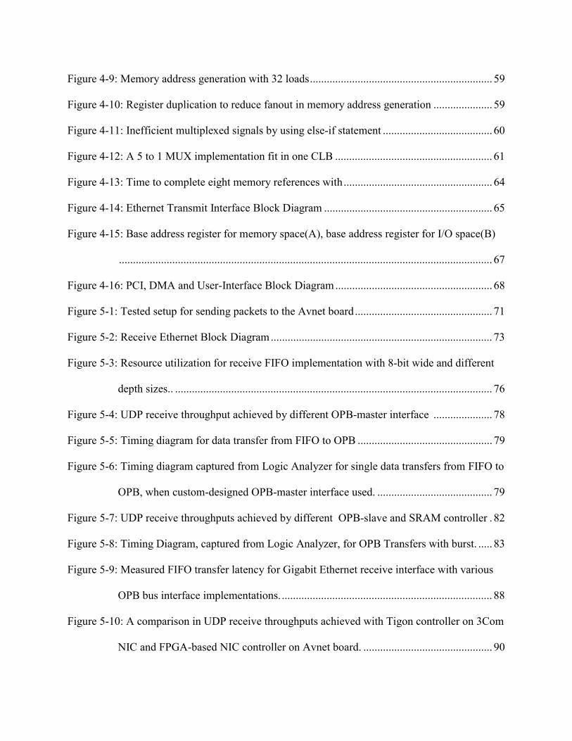
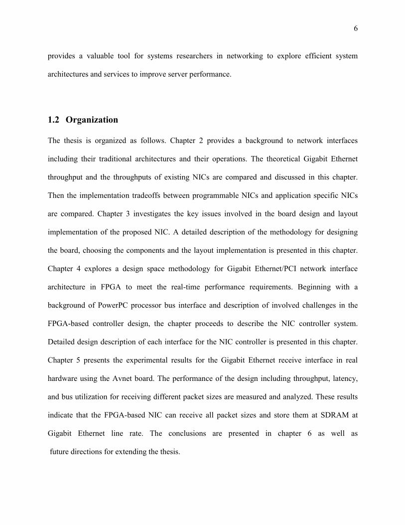
the network. The steps for sending packets from the main memory to the network are shown in
Figure 2.1(A). To send packets, the host processor first instructs the NIC to transfer packets from
the main memory through a programmed I/O in step 1. In step 2, the NIC initiates DMA
transfers to move packets from the main memory to the local memory. In step 3, packets need to
be buffered in the Buffer-TX, waiting for the MAC to allow transmission. Once the packet
transfer to local memory is complete, the NIC sends the packet out to the network through its
MAC unit in step 4. Finally, the NIC informs the host operating system that the packet has been
sent over the
network in step 5.
Figure 2.1: (A) Steps for sending packets to the network, (B) Steps for receiving packets from the network
The steps for receiving packets from the network are shown in Figure 2.1(B). A packet, which
has arrived from the network, is received by the MAC unit in step 1 and stored in the Buffer-RX
in step 2. In step 3, the NIC initiates DMA transfers to send the packet from local memory to the
main memory. Finally, when the packet is stored in main memory the NIC notifies the host
(B) (A)
Network
Main Memory
DMA
Controller
MAC
PacketHost
Processor
Local Memory
Buffer-TX
Buffer-RX Packet
PCI Interface
5 1
2
3
4
Packet
Network
Main Memory
DMA
Controller
MAC
PacketHost
Processor
Local Memory
Buffer-TX
Buffer-RX Packet
PCI Interface
Packet
4
2 3
1
9
operating system about the new packet in the main memory in step 4. Mailboxes are locations,
which are used to facilitate communication between host processors and network interfaces.
Typically, these locations are written by one processor and cause an interrupt to the other
processor or controller in the NIC. The value written may or may not have any significance. The
NIC can map some of its local memory onto the PCI bus, which functions as a mailbox file.
Therefore, these mailboxes are accessible by both host processor and the controller in the NIC.
The serial Gigabit Ethernet transmit and receive interfaces can communicate with the controller
in the NIC by using descriptors. For transmit packets, the descriptors contain the starting address
and length of each packet. For receive packets the descriptors contain the starting address and
length of the packet as well as indication of any unusual or error events detected during the
reception of the packet.
2.2 Programmable NICs Compared with Application Specifics NICs In a programmable NIC, a programmable processor controls the steps shown in Figure 2.1 (A)
and (B), while fixed state machines control these steps in ASIC-based NICs. A programmable
NIC provides the flexibility to implement new services in order to improve and modify the
functionality of the NIC. With a programmable network interface, it is easy to implement value-
added network services like iSCSI [31] or network interface data caching [20], which
substantially can improve networking server performance. iSCSI provides SCSI-like access to
remote storage using the traditional TCP/IP protocols as their transport layer. iSCSI has emerged
as a popular protocol for network storage servers recently. By using inexpensive and ubiquitous
TCP/IP network rather than expensive proprietary application-specific networks, iSCSI is
gaining popularity. Several iSCSI adapters aim to improve storage server performance by
offloading the complete implementation of the TCP/IP protocols or a subset of the protocol
10
processing on the adapters. In addition, previous research shows that network interface data
caching is a novel network service on programmable network interfaces to exploit their storage
capacity as well as computation power in order to alleviate local interconnect bottleneck. By
storing frequently requested files in this cache, the server will not need to send those files across
the interconnect for each request [19, 20]. This technique allows frequently requested content to
be cached directly on the network interface. Experimental results indicate that using a 16MB
DRAM or less on the network interface can effectively reduce local interconnect traffic which
substantially improves server performance.
Such new services may be significantly more complex than the existing services and it is
costly to implement and maintain them in non-programmable ASIC-based NICs with a fixed
architecture. However, existing programmable network interfaces do not provide enough
computational power and memory capacity to implement these services efficiently.
Programmable processors provide flexibility by running some functions as software, but that
flexibility comes at the expense of lower performance and higher power consumption than with
ASICs. In a programmable processor, there are several steps for the execution of the instruction
including Instruction Fetching, Decoding, Execution, Memory access and Write back to registers
which slows down the processor performance.
2.3 Previous Programmable NICs This section explains some previous work on programmable NICs. Previous researches have
focused on developing software-based NICs. Many of these platforms use standard
microprocessors, like the Intel Pentium, AMD Athlon, or the Motorla/IBM PowerPC.
11
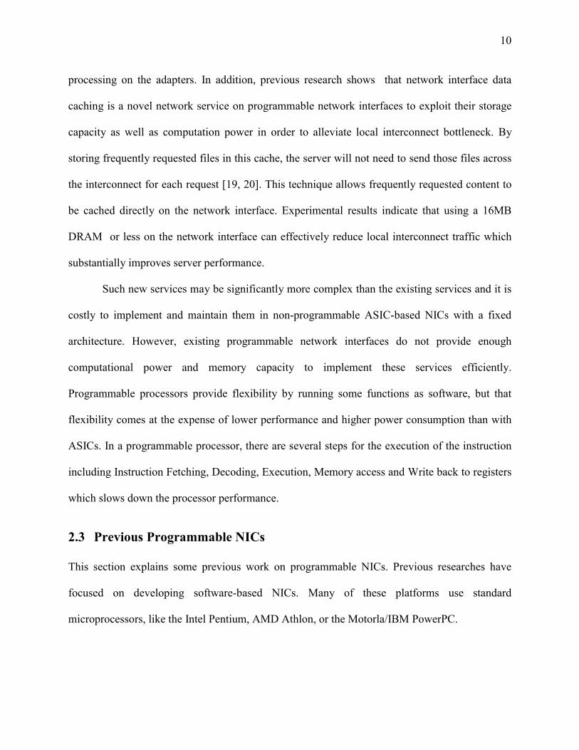
Myrinet LANai is a very popular programmable NIC, which is based on a system area network,
called Myrinet [8, 45, 52, 60]. The block diagram of the Myrinet-2000-Fiber/PCI interface is
shown in Figure 2.2.
Figure 2.2: Block diagram of M3F-PCI64, universal, 64/32-bit, 66/33MHz, Myrinet-2000-Fiber/PCI interface[45]
The interface processor includes LANai 9 RISC operating at up to 133MHz for the PCI64B
interfaces, or at up to 200MHz for the PCI64C interfaces. The on-board memory is a fast SRAM,
ranging from 2MB up to 8MB depending on the revision of the board. The local memory
operates from the same clock as the RISC, i.e., at up to 133 MHz for the PCI64B interfaces, or at
up to 200MHz for the PCI64C interfaces. The PCI-bus interface, 66/33MHz, is capable of PCI
data rates approaching the limits of the PCI bus (528 MB/s for 64-bit, 66MHz; 264 MB/s for 64-
bit, 33MHz or 32-bit, 66MHz; 132 MB/s for 32-bit, 33MHz). However, the data rate to/from
system memory will depend upon the host's memory and PCI-bus implementation. The DMA
controller allows multiple DMA transfers in PCI interface. A few projects used these
programmable network interfaces ranging from implementing various optimizations for basic
12
send and receive processing to implementing all or parts of network protocol processing on the
network interface.
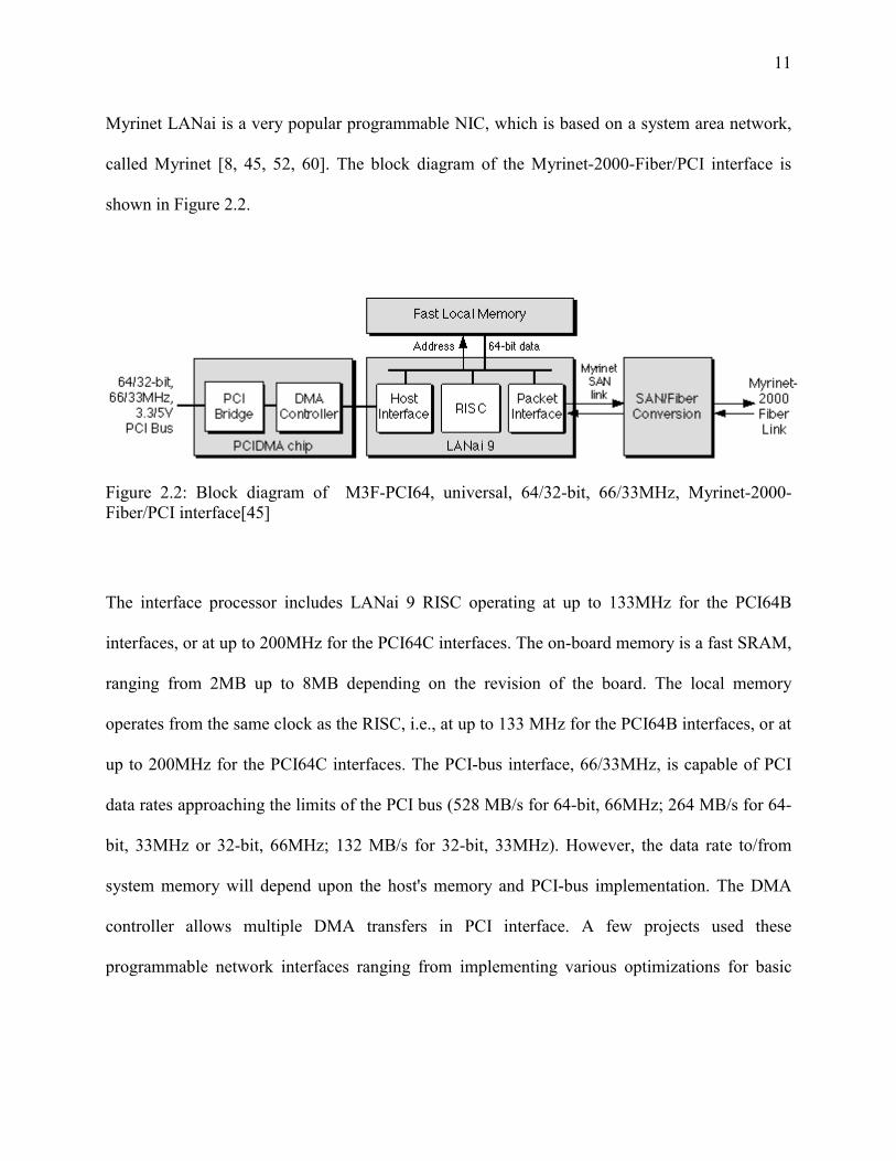
The Tigon is another representative programmable Ethernet controller that provides
several mechanisms to support parallel and event-driven firmware [4, 5]. Figure 2.3 shows a
block diagram of the Tigon controller.
Figure 2.3: Block diagram of Tigon controller [19]
The Tigon has two 88 MHz single issue, in-order embedded processors that are based on
the MIPS R4000. The processors share access to external SRAM. Each processor also has a
private on-chip scratch pad memory, which serves as a low-latency software-managed cache.
Depending on the Tigon revision, the SRAM size varies from 2Kbyte to 16Kbyte for each
processor. The 3Com 710024 Gigabit Ethernet network interface cards are based on the Tigon
controller and have 1 MB of external SRAM. The Tigon programmable Ethernet controller
supports a PCI host interface at 33MHz or 66MHz and a full-duplex Gigabit Ethernet interface.
13
Kim showed in [20] that caching data directly on a programmable network interface reduces
local interconnect traffic on networking servers by eliminating repeated transfers of frequently-
requested content. Experimental results on Tigon- based NICs indicate that the prototype
implementation of network interface data caching reduces PCI bus traffic by 35–58% on four
web workloads with only 16MB cache, which was prototyped on an external DRAM memory.
The Quadrics network uses programmable network interfaces called Elan to support
specialized services for high performance clusters [14, 15, 51]. Like Myrinet, the Quadrics
network provides high performance messaging system using special-purpose network interfaces,
switches, and links. However, the Quadrics network provides much greater transmission
bandwidth of 400MBps as opposed to 250MBps of Myrinet.
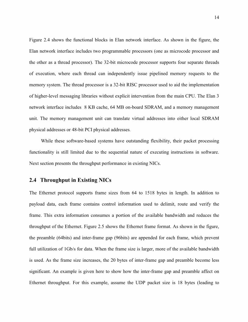
Figure 2.4: Block diagram of Elan functional units in Quadrics NIC [15]
14
Figure 2.4 shows the functional blocks in Elan network interface. As shown in the figure, the
Elan network interface includes two programmable processors (one as microcode processor and
the other as a thread processor). The 32-bit microcode processor supports four separate threads
of execution, where each thread can independently issue pipelined memory requests to the
memory system. The thread processor is a 32-bit RISC processor used to aid the implementation
of higher-level messaging libraries without explicit intervention from the main CPU. The Elan 3
network interface includes 8 KB cache, 64 MB on-board SDRAM, and a memory management
unit. The memory management unit can translate virtual addresses into either local SDRAM
physical addresses or 48-bit PCI physical addresses.
While these software-based systems have outstanding flexibility, their packet processing
functionality is still limited due to the sequential nature of executing instructions in software.
Next section presents the throughput performance in existing NICs.
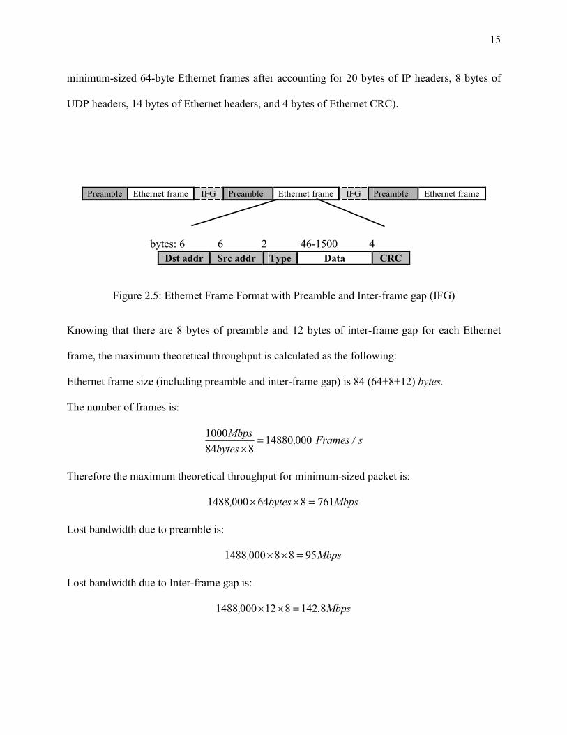
2.4 Throughput in Existing NICs The Ethernet protocol supports frame sizes from 64 to 1518 bytes in length. In addition to
payload data, each frame contains control information used to delimit, route and verify the
frame. This extra information consumes a portion of the available bandwidth and reduces the
throughput of the Ethernet. Figure 2.5 shows the Ethernet frame format. As shown in the figure,
the preamble (64bits) and inter-frame gap (96bits) are appended for each frame, which prevent
full utilization of 1Gb/s for data. When the frame size is larger, more of the available bandwidth
is used. As the frame size increases, the 20 bytes of inter-frame gap and preamble become less
significant. An example is given here to show how the inter-frame gap and preamble affect on
Ethernet throughput. For this example, assume the UDP packet size is 18 bytes (leading to
15
minimum-sized 64-byte Ethernet frames after accounting for 20 bytes of IP headers, 8 bytes of
UDP headers, 14 bytes of Ethernet headers, and 4 bytes of Ethernet CRC).
Preamble Ethernet frame IFG Preamble Ethernet frame IFG Preamble Ethernet frame
Dst addr Src addr Type Data CRC
Figure 2.5: Ethernet Frame Format with Preamble and Inter-frame gap (IFG)
Knowing that there are 8 bytes of preamble and 12 bytes of inter-frame gap for each Ethernet
frame, the maximum theoretical throughput is calculated as the following:
Ethernet frame size (including preamble and inter-frame gap) is 84 (64+8+12) bytes.
The number of frames is:
s/Frames,bytes
Mbps 00014880884
1000 =×
Therefore the maximum theoretical throughput for minimum-sized packet is:
Mbpsbytes, 7618640001488 =××
Lost bandwidth due to preamble is:
Mbps, 95880001488 =××
Lost bandwidth due to Inter-frame gap is:
Mbps., 81428120001488 =××
bytes: 6 6 2 46-1500 4
16
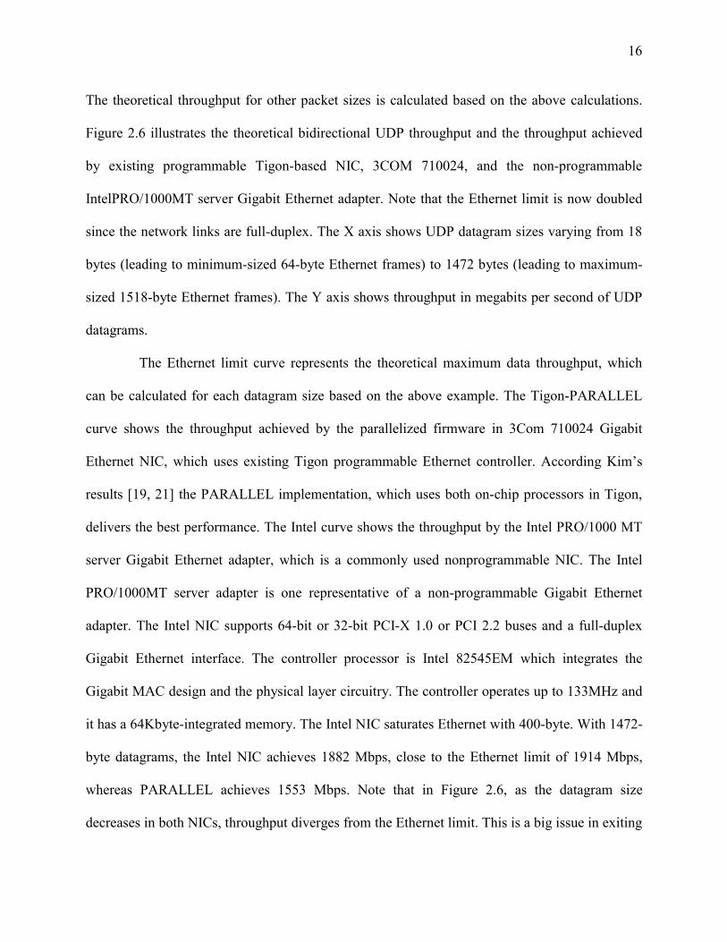
The theoretical throughput for other packet sizes is calculated based on the above calculations.
Figure 2.6 illustrates the theoretical bidirectional UDP throughput and the throughput achieved
by existing programmable Tigon-based NIC, 3COM 710024, and the non-programmable
IntelPRO/1000MT server Gigabit Ethernet adapter. Note that the Ethernet limit is now doubled
since the network links are full-duplex. The X axis shows UDP datagram sizes varying from 18
bytes (leading to minimum-sized 64-byte Ethernet frames) to 1472 bytes (leading to maximum-
sized 1518-byte Ethernet frames). The Y axis shows throughput in megabits per second of UDP
datagrams.
The Ethernet limit curve represents the theoretical maximum data throughput, which
can be calculated for each datagram size based on the above example. The Tigon-PARALLEL
curve shows the throughput achieved by the parallelized firmware in 3Com 710024 Gigabit
Ethernet NIC, which uses existing Tigon programmable Ethernet controller. According Kim’s
results [19, 21] the PARALLEL implementation, which uses both on-chip processors in Tigon,
delivers the best performance. The Intel curve shows the throughput by the Intel PRO/1000 MT
server Gigabit Ethernet adapter, which is a commonly used nonprogrammable NIC. The Intel
PRO/1000MT server adapter is one representative of a non-programmable Gigabit Ethernet
adapter. The Intel NIC supports 64-bit or 32-bit PCI-X 1.0 or PCI 2.2 buses and a full-duplex
Gigabit Ethernet interface. The controller processor is Intel 82545EM which integrates the
Gigabit MAC design and the physical layer circuitry. The controller operates up to 133MHz and
it has a 64Kbyte-integrated memory. The Intel NIC saturates Ethernet with 400-byte. With 1472-
byte datagrams, the Intel NIC achieves 1882 Mbps, close to the Ethernet limit of 1914 Mbps,
whereas PARALLEL achieves 1553 Mbps. Note that in Figure 2.6, as the datagram size
decreases in both NICs, throughput diverges from the Ethernet limit. This is a big issue in exiting
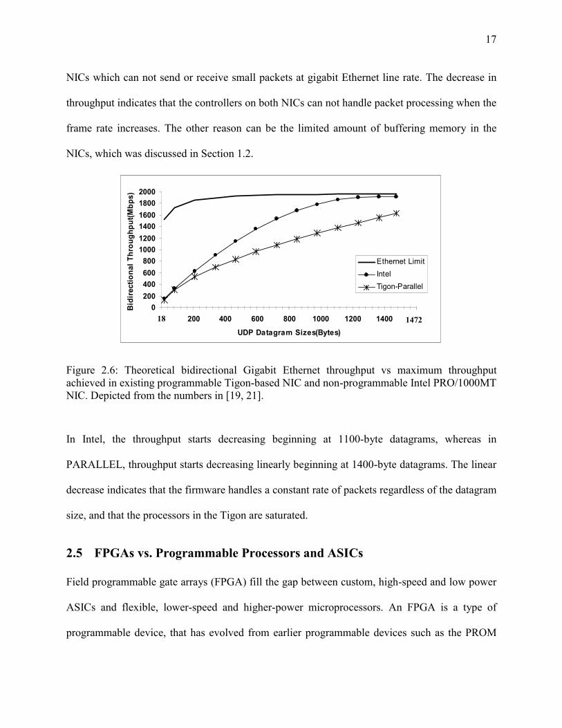
17
NICs which can not send or receive small packets at gigabit Ethernet line rate. The decrease in
throughput indicates that the controllers on both NICs can not handle packet processing when the
frame rate increases. The other reason can be the limited amount of buffering memory in the
NICs, which was discussed in Section 1.2.
0200400600800
100012001400160018002000
0 200 400 600 800 1000 1200 1400 1600
UDP Datagram Sizes(Bytes)
Bid
irec
tiona
l Thr
ough
put(M
bps)
Ethernet LimitIntelTigon-Parallel
Figure 2.6: Theoretical bidirectional Gigabit Ethernet throughput vs machieved in existing programmable Tigon-based NIC and non-programmableNIC. Depicted from the numbers in [19, 21].
In Intel, the throughput starts decreasing beginning at 1100-byte data
PARALLEL, throughput starts decreasing linearly beginning at 1400-byte da
decrease indicates that the firmware handles a constant rate of packets regard
size, and that the processors in the Tigon are saturated.
2.5 FPGAs vs. Programmable Processors and ASICs Field programmable gate arrays (FPGA) fill the gap between custom, high-s
ASICs and flexible, lower-speed and higher-power microprocessors. An
programmable device, that has evolved from earlier programmable devices
1472 18
aximum throughput Intel PRO/1000MT
grams, whereas in
tagrams. The linear
less of the datagram
peed and low power
FPGA is a type of
such as the PROM
18
(Programmable Read-only memory), the PLD (Programmable logic device), and the MPGA
(Mask Programmable Gate Array) [64]. An FPGA is an IC (integrated circuit) consisting of an
array of programmable cells. Each cell can be configured to program any logic function. The
logic cells are connected using configurable, electrically erasable static-random-access memory
(SRAM) cells that change the FPGA’s interconnection structure. Just as a software program
determines the functions executed by microprocessor, the configuration of FPGA determined its
functionality. Novel functions can be programmed into FPGA by downloading a new
configuration, similar to the way a microprocessor can be reprogrammed by downloading a new
software code. However, in contrast to microprocessor’s functions, the FPGA runs in hardware.
Therefore, there is no software’s relatively instruction overhead, which results in higher speed
and lower power dissipation for FPGAs than microprocessors.
FPGAs provide a new approach to Application Specific Integrated Circuit (ASIC)
implementation that features both large scale integration and user programmability. Short
turnaround time and low manufacturing cost have made FPGA technology popular for rapid
system prototyping and low to medium-volume production. FPGA platforms are easily
configurable, and with a growing number of hard cores for memory, clock management, and I/O,
combined with flexible soft cores, FPGAs provide a highly flexible platform for developing
programmable network interfaces. Although ASIC design is compact and less expensive when
the product volume is large, it is not easy to configure at the stage of prototyping. FPGA
provides hardware programmability and the flexibility to study several new designs in hardware
architectures. It can easily achieve the concept of system-on-chip (SOC) with hardware
configuration. When the design is mature, FPGA design can be easily converted to system on a
chip for mass production. The increase in complexity of FPGAs in recent years has made it
19
possible to implement more complex hardware systems that once required application-specific
integrated. Current devices provide 200 to 300 thousand logic gate equivalents plus 100 to 200
thousand bits of static RAM [65].
Although FPGAs deliver higher performance than programmable processors, they still
have a lot of setup overhead compared to ASICs, requiring as many as 20 transistors to
accomplish what an ASIC does with one [47]. This adds latency and increases the power
consumption in the design. In addition, FPGAs are more sensitive to coding styles and design
practices. In many cases, slight modification in coding practices can improve the system
performance from 10% to 100% [73]. Thus, for complex and high-speed designs, current FPGAs
are still slow and power-hungry and they come with high transistor overhead. This makes FPGA
designers face with additional challenges of architectures to meet difficult performance goals and
different implementation strategies.
2.6 Previous FPGA-based Network Interfaces Field Programmable Gate Array has proven to be an effective technology for implementation of
networking hardware. Although, there is no research done on FPGA-based network interface
card yet, there are a few on-going FPGA-based networking researches in university and industry,
which are explained in this section.
In the development of the iPOINT (Illinois Pulsar-based Interconnection) testbed, a
complete Asynchronous Transfer Mode (ATM) switch was built using FPGAs [32]. This
research platform is established to design and develop scalable ATM switch architecture and
investigate new techniques for data queuing. Within the testbed, the FPGA is used to prototype
the core logic of the ATM switch, scheduler, and queue modules. This system utilized a Xilinx
20
4013 FPGA to implement a single-stage switch and multiple Xilinx 4005 FPGAs to implement
queuing modules at each of the inputs of the switch.
The Illinois Input Queue (iiQueue) was implemented to enhance the performance of distributed
input queuing by sorted packets according to their flow, destination, and priority. A prototype of
this system was implemented using Xilinx XC4013 FPGAs [17]. The benefit of using
reprogrammable logic in the iiQueue was that complex algorithms for queuing data could be
tuned by simply reprogramming the FPGA logic.
The FPX, field programmable extender, is an open hardware platform designed and
implemented at Washington University that can be used to implement OC-48 speed packet
processing functions in reconfigurable hardware [16, 33, 34]. The FPX provides a mechanism for
networking hardware modules to be dynamically loaded into a running system. The FPX
includes two FPGAs, five banks of memory, and two high-speed network interfaces. The FPX
implements all logic using two FPGA devices: the Network Interface Device (NID) is
implemented with a Virtex 600E-fg676 FPGA and the Reprogrammable Application Device
(RAD), implemented with a Xilinx Virtex 1000E-fg680 FPGA. The RAD contains the modules
that implement customized packet processing functions. Each module on the RAD includes one
SRAM and one wide Synchronous Dynamic RAM (SDRAM). The Network Interface Device
(NID) on the FPX controls how packet flows are routed to and from modules.
The Cal Poly Intelligent Network Interface Card (CiNIC) is a platform that partitions the
network application and runs most of the network processing on an FPGA based coprocessor
[87]. The main idea is to assign all the network tasks to the coprocessor on the NIC so that the
host CPU can be used for non-network related tasks. The research group uses the PCISYS
development boards from PLDA with Altera’s FPGA.
21
Besides the academic efforts mentioned above, industrial efforts are being made to use FPGAs in
networking projects.
ATLAS Inc. released an FPGA-based Gigabit Ethernet S-LINK link source card (LSC) in
late 2001[35]. This board is used as a research platform for S-Link protocol prototyping. The
function of the card is to receive a stream of words in S-LINK format, i.e. 32-bit data and control
words, via the standard S-Link connector. Then it outputs the data words as one or more Ethernet
frames. The FPGA is implemented by an Altera 10K50V and is configured via the on-board
EPROM. The board contains an 18Mb synchronous SRAM, which is used for data storage. The
FPGA provides the functionality to write event data from the FIFO to the onboard SRAM or to
the MAC for transfer via Gigabit Ethernet or to the on-board SRAM, and to transfer data stored
in the SRAM to the MAC for transfer via Gigabit Ethernet if requested by the target.
As mentioned earlier, when we intended to send the printer circuit board (PCB) of our
FPBA-based NIC for fabrication, Avnet Company released their Virtex-II Pro Development Kit.
This board is built around an extremely flexible FPGA-based development platform, which
includes two FPGAs, a 64-bit 33/66MHz PCI Connector, a Gigabit Ethernet PHY and multiple
memories. Although the Avnet board was not built to be a functional NIC, since it was close
enough to our design we decided to use this board to evaluate the NIC controller design.
Bruce Oakley, from Amirix Inc., proposed a configurable network interface solution on a
standard platform in 2002 [7]. The platform was based on an industry standard mezzanine card
format supporting multiple network interfaces, including 10/100 Mbps Ethernet and ATM.
Configurability was based on an Virtex-II Pro FPGA with an embedded processor. Then the
Amirix Company released an FPGA PCI platform development board based on this proposal on
November 2003. Since this board came after the Avnet board there was no access to do research
22
on this board. However, the Amirix board can not meet our requirements since is supports
10/100Mbps Ethernet and 32bit 66MHz PCI bus.
2.7 Summary As researchers vigorously develop advanced, processing schemes for programmable networks
there exists a need for a scalable network interface architecture capable of data processing at line
speeds. Existing network interface architectures that provide sufficient flexibility employ
software processing environments containing multiple Reduced Instruction Set Computer (RISC)
cores and suffer from lower performance. Existing high performance network interface
architectures capable of data processing at high speeds employ Application Specific Integrated
Circuits (ASICs) to perform parallel computations in hardware, but provide limited flexibility for
deployment of new applications or protocols, and necessitate longer design cycles and higher
costs than software-based solutions.
However, the previous approaches do not focus on designing network interface
architectures with both flexibility available in software and the performance offered by hardware.
These previous approaches also do not provide ample memory resources to cover the design
space of potential applications.
23
Chapter 3
3 Board Design and Layout Implementation
Designing the FPGA-based PCI/Gigabit Ethernet NIC proposed in this thesis involves additional
issues, which govern the decision for board design and affect on choosing the components of the
NIC. The key issues are maximum power limit in PCI card, power consumption of the on-board
components, maximum achievable bandwidth for each component, clock distribution and
management in different clock domains, power distribution system in the FPGAs and high-speed
signaling constraints in layout implementation. To meet these challenges, a methodology for
designing the board, choosing components, and implementing the PCB layout is presented in this
chapter.
3.1 The FPGA-based NIC Hardware Platform The FPGA-based Gigabit Ethernet/PCI Network Interface Card (NIC) is designed to provide
either a full or a half-duplex Gigabit Ethernet interface. The NIC connects the PCI-compliant
server to a Gigabit Ethernet network and is implemented for use in systems that support either
the 64 or 32 bit wide PCI Local Bus operating at 66 or 33 MHz. The block diagram of the NIC is
shown in Figure 3.1.
24
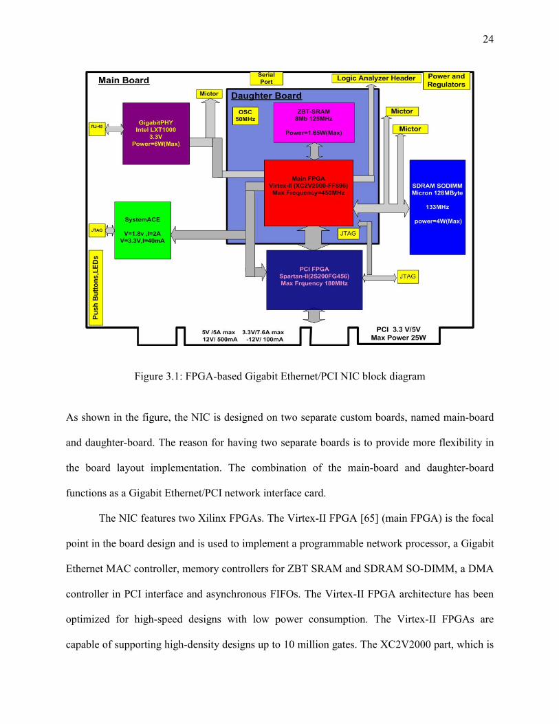
Figure 3.1: FPGA-based Gigabit Ethernet/PCI NIC block diagram
As shown in the figure, the NIC is designed on two separate custom boards, named main-board
and daughter-board. The reason for having two separate boards is to provide more flexibility in
the board layout implementation. The combination of the main-board and daughter-board
functions as a Gigabit Ethernet/PCI network interface card.
The NIC features two Xilinx FPGAs. The Virtex-II FPGA [65] (main FPGA) is the focal
point in the board design and is used to implement a programmable network processor, a Gigabit
Ethernet MAC controller, memory controllers for ZBT SRAM and SDRAM SO-DIMM, a DMA
controller in PCI interface and asynchronous FIFOs. The Virtex-II FPGA architecture has been
optimized for high-speed designs with low power consumption. The Virtex-II FPGAs are
capable of supporting high-density designs up to 10 million gates. The XC2V2000 part, which is
25
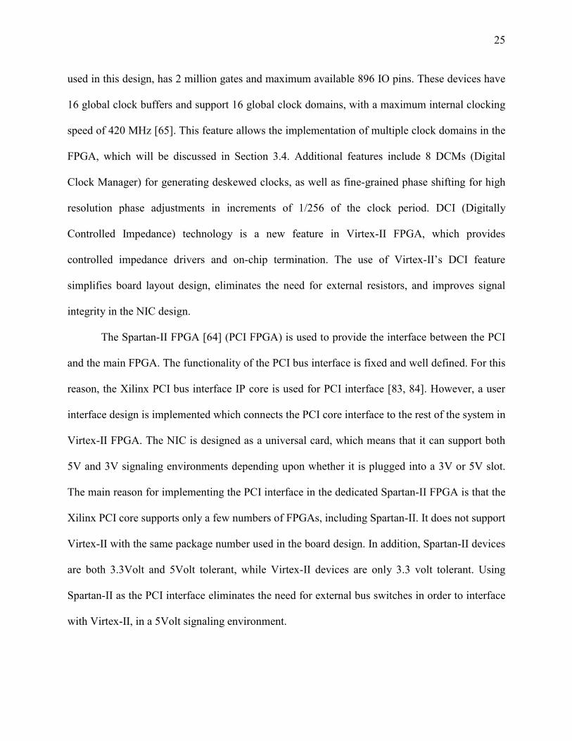
used in this design, has 2 million gates and maximum available 896 IO pins. These devices have
16 global clock buffers and support 16 global clock domains, with a maximum internal clocking
speed of 420 MHz [65]. This feature allows the implementation of multiple clock domains in the
FPGA, which will be discussed in Section 3.4. Additional features include 8 DCMs (Digital
Clock Manager) for generating deskewed clocks, as well as fine-grained phase shifting for high
resolution phase adjustments in increments of 1/256 of the clock period. DCI (Digitally
Controlled Impedance) technology is a new feature in Virtex-II FPGA, which provides
controlled impedance drivers and on-chip termination. The use of Virtex-II’s DCI feature
simplifies board layout design, eliminates the need for external resistors, and improves signal
integrity in the NIC design.
The Spartan-II FPGA [64] (PCI FPGA) is used to provide the interface between the PCI
and the main FPGA. The functionality of the PCI bus interface is fixed and well defined. For this
reason, the Xilinx PCI bus interface IP core is used for PCI interface [83, 84]. However, a user
interface design is implemented which connects the PCI core interface to the rest of the system in
Virtex-II FPGA. The NIC is designed as a universal card, which means that it can support both
5V and 3V signaling environments depending upon whether it is plugged into a 3V or 5V slot.
The main reason for implementing the PCI interface in the dedicated Spartan-II FPGA is that the
Xilinx PCI core supports only a few numbers of FPGAs, including Spartan-II. It does not support
Virtex-II with the same package number used in the board design. In addition, Spartan-II devices
are both 3.3Volt and 5Volt tolerant, while Virtex-II devices are only 3.3 volt tolerant. Using
Spartan-II as the PCI interface eliminates the need for external bus switches in order to interface
with Virtex-II, in a 5Volt signaling environment.
26
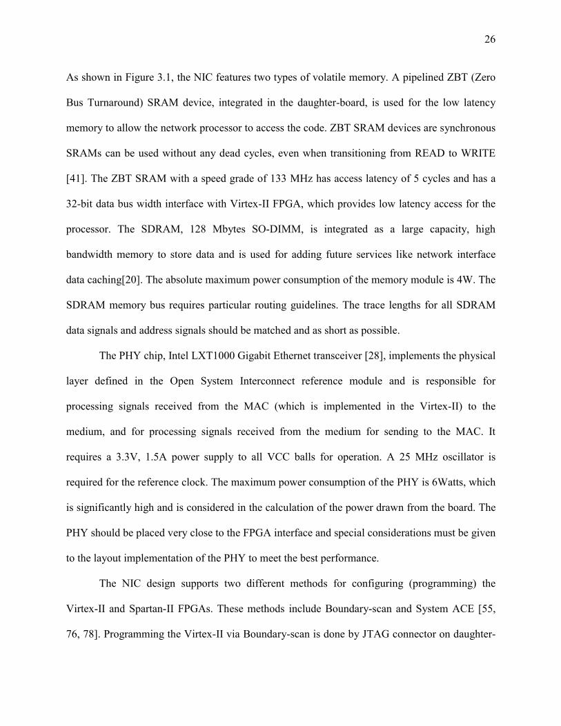
As shown in Figure 3.1, the NIC features two types of volatile memory. A pipelined ZBT (Zero
Bus Turnaround) SRAM device, integrated in the daughter-board, is used for the low latency
memory to allow the network processor to access the code. ZBT SRAM devices are synchronous
SRAMs can be used without any dead cycles, even when transitioning from READ to WRITE
[41]. The ZBT SRAM with a speed grade of 133 MHz has access latency of 5 cycles and has a
32-bit data bus width interface with Virtex-II FPGA, which provides low latency access for the
processor. The SDRAM, 128 Mbytes SO-DIMM, is integrated as a large capacity, high
bandwidth memory to store data and is used for adding future services like network interface
data caching[20]. The absolute maximum power consumption of the memory module is 4W. The
SDRAM memory bus requires particular routing guidelines. The trace lengths for all SDRAM
data signals and address signals should be matched and as short as possible.
The PHY chip, Intel LXT1000 Gigabit Ethernet transceiver [28], implements the physical
layer defined in the Open System Interconnect reference module and is responsible for
processing signals received from the MAC (which is implemented in the Virtex-II) to the
medium, and for processing signals received from the medium for sending to the MAC. It
requires a 3.3V, 1.5A power supply to all VCC balls for operation. A 25 MHz oscillator is
required for the reference clock. The maximum power consumption of the PHY is 6Watts, which
is significantly high and is considered in the calculation of the power drawn from the board. The
PHY should be placed very close to the FPGA interface and special considerations must be given
to the layout implementation of the PHY to meet the best performance.
The NIC design supports two different methods for configuring (programming) the
Virtex-II and Spartan-II FPGAs. These methods include Boundary-scan and System ACE [55,
76, 78]. Programming the Virtex-II via Boundary-scan is done by JTAG connector on daughter-
27
board. The JTAG connector on the main-board is for programming the Spartan-II via Boundary-
scan. The iMPACT software in Xilinx ISE tools is used to program the FPGA devices by
transferring bit files from the design environment to the NIC [82]. Configuring the Virtex-II and
Spartan-II FPGAs with the System ACE is another way of transferring bit files from the design
environment to the board. The system ACE family is a pre-engineered, high-density
configuration solution in multiple FPGA systems. It allows managing multiple bit streams to be
stored on the on-chip flash memory for immediate FPGA configuration. As shown in Figure 3.1,
the main-board is designed to have system ACE MPM (multi-package module) [76]. The MPM
consists of an on-chip AMD flash memory with 64 Mb densities, a non-volatile PROM and a
Xilinx Virtex-E configuration controller. The Virtex-II and Spartan-II FPGAs can be configured
through Select MAP mode, which is the fastest configuration mode with maximum configuration
speed of 152Mb/s [78].
As shown in Figure 3.1, three AMP Mictor connectors [2] on the main board, compatible
with Tektronix logic analyzers, provide high-speed signals that can be used for debugging the
signals between SDRAM and Virtex-II or the PHY and Virtex-II FPGA. A 50-pin Logic
Analyzer header connector provides access to additional pins in the Virtex-II FPGA for
debugging purposes. A number of LEDs and pushbuttons are also on the board for testing
purposes. The daughter-board is connected to the main board by eight dedicated connectors. The
Virtex-II FPGA on the daughter-board has access to the PHY, Spartan-II FPGA, SDRAM, and
the System ACE via these connectors.
3.2 Plan for Gigabit Ethernet Throughput To achieve one Gigabit per second throughput in the FPGA-based Gigabit Ethernet/PCI NIC, the
major functional components in the NIC should provide minimum bandwidth of 1Gbps. These
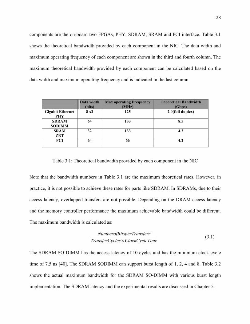
28
components are the on-board two FPGAs, PHY, SDRAM, SRAM and PCI interface. Table 3.1
shows the theoretical bandwidth provided by each component in the NIC. The data width and
maximum operating frequency of each component are shown in the third and fourth column. The
maximum theoretical bandwidth provided by each component can be calculated based on the
data width and maximum operating frequency and is indicated in the last column.
Data width (bits)
Max operating Frequency (MHz)
Theoretical Bandwidth (Gbps)
Gigabit Ethernet PHY
8 x2 125 2.0(full duplex)
SDRAM SODIMM
64 133 8.5
SRAM ZBT
32 133 4.2
PCI 64 66 4.2
Table 3.1: Theoretical bandwidth provided by each component in the NIC
Note that the bandwidth numbers in Table 3.1 are the maximum theoretical rates. However, in
practice, it is not possible to achieve these rates for parts like SDRAM. In SDRAMs, due to their
access latency, overlapped transfers are not possible. Depending on the DRAM access latency
and the memory controller performance the maximum achievable bandwidth could be different.
The maximum bandwidth is calculated as:
TimeClockCycleclesTransferCy
ferrtsperTransNumberofBi×
(3.1)
The SDRAM SO-DIMM has the access latency of 10 cycles and has the minimum clock cycle
time of 7.5 ns [40]. The SDRAM SODIMM can support burst length of 1, 2, 4 and 8. Table 3.2
shows the actual maximum bandwidth for the SDRAM SO-DIMM with various burst length
implementation. The SDRAM latency and the experimental results are discussed in Chapter 5.
29
Burst Length
Transfer cycles
Number of bits per Transfer
Max Practical Bandwidth (Mbps)
Burst-1 (single transfer)
10 64 853.3
Burst-2 12 64x 2 1422.2
Burst-4 14 64 x 4 2438.0
Burst-8 18 64x 8 3792.5
Table 3.2: practical bandwidth in SDRAM SODIMM
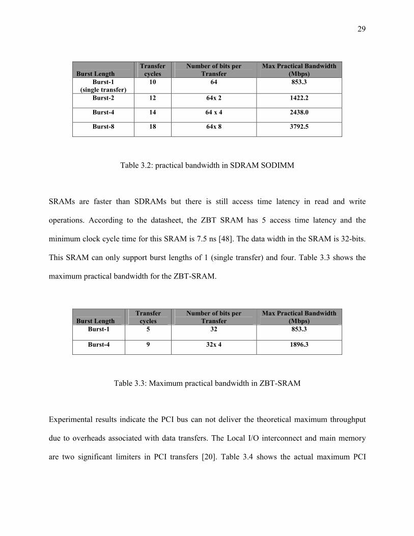
SRAMs are faster than SDRAMs but there is still access time latency in read and write
operations. According to the datasheet, the ZBT SRAM has 5 access time latency and the
minimum clock cycle time for this SRAM is 7.5 ns [48]. The data width in the SRAM is 32-bits.
This SRAM can only support burst lengths of 1 (single transfer) and four. Table 3.3 shows the
maximum practical bandwidth for the ZBT-SRAM.
Burst Length
Transfer cycles
Number of bits per Transfer
Max Practical Bandwidth (Mbps)
Burst-1 5 32 853.3
Burst-4 9 32x 4 1896.3
Table 3.3: Maximum practical bandwidth in ZBT-SRAM
Experimental results indicate the PCI bus can not deliver the theoretical maximum throughput
due to overheads associated with data transfers. The Local I/O interconnect and main memory
are two significant limiters in PCI transfers [20]. Table 3.4 shows the actual maximum PCI
30
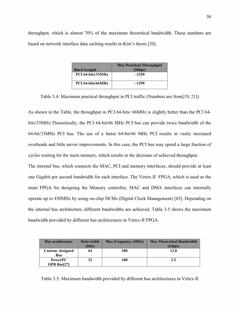
throughput, which is almost 70% of the maximum theoretical bandwidth. These numbers are
based on network interface data caching results in Kim’s thesis [20].
Burst Length
Max Practical Throughput (Mbps)
PCI 64-bits/33MHz ~1250
PCI 64-bits/66MHz ~1290
Table 3.4: Maximum practical throughput in PCI traffic (Numbers are from[19, 21])
As shown in the Table, the throughput in PCI 64-bits/ 66MHz is slightly better than the PCI 64-
bits/33MHz.Theoretically, the PCI 64-bit/66 MHz PCI bus can provide twice bandwidth of the
64-bit/33MHz PCI bus. The use of a faster 64-bit/66 MHz PCI results in vastly increased
overheads and little server improvements. In this case, the PCI bus may spend a large fraction of
cycles waiting for the main memory, which results in the decrease of achieved throughput.
The internal bus, which connects the MAC, PCI and memory interfaces, should provide at least
one Gigabit per second bandwidth for each interface. The Virtex-II FPGA, which is used as the
main FPGA for designing the Memory controller, MAC and DMA interfaces can internally
operate up to 450MHz by using on-chip DCMs (Digital Clock Management) [65]. Depending on
the internal bus architecture, different bandwidths are achieved. Table 3.5 shows the maximum
bandwidth provided by different bus architectures in Virtex-II FPGA.
Bus architecture Data width (bits)
Max Frequency (MHz) Max Theoretical Bandwidth (Gbps)
Custom- designed Bus
64 200 12.8
PowerPC OPB Bus[27]
32 100 3.2
Table 3.5: Maximum bandwidth provided by different bus architectures in Virtex-II
31
The custom-designed bus was originally used for the internal system bus. Simulation results
indicate that the custom-designed bus bandwidth can achieve up to 12.8 Gbps with adding
pipeline stages in controller architecture. The PowerPC OPB (On-chip Peripheral Bus) bus is
provided by Xilinx [27]. As shown in Table 3.5, PowerPC OPB bus bandwidth is only 3.2 Gbps,
which is not enough for each interface to achieve the maximum Gigabit throughput. The
architecture design with OPB bus and the performance results are respectively discussed in
Section 3.2 and 5.2. Spartan-II FPGA, which implements the PCI interface, should provide
minimum 2Gbps throughput at the PCI bus interface for bidirectional DMA transfers.
3.3 Board Power Requirement The total power drawn collectively from all four power-rails for the PCI card cannot exceed 25
watts [48]. Due to this maximum PCI power limit, the maximum power consumption of the
components on the main-board and daughter-board should be less than 25 watts. Otherwise, an
external power supply is required to provide power to the board. The absolute power
consumption of each component depends on many factors such as device architecture and
manufacturer. Finding low power components, which provide the desired functionality, price and
availability, is an additional issue in the board design. For example, the absolute power
consumption for Micron SDRAM SODIMM varies significantly with the memory size. The
maximum power consumption of 128Mbytes SODIMM is 4Watts, whereas the maximum power
consumption for 512 Mbytes SDRAM SODIMM is 16 Watts with the same architecture.
Another noticeable fact is that the power consumption within an FPGA is design-dependent and
can be difficult to calculate prior to implementing the design. Most other large, dense ICs (such
as large microprocessors) are only designed to implement specific tasks in their hard silicon.
32
Thus, their power supply demands are fixed and only fluctuate within a certain range. FPGAs do
not share this property. Since FPGAs can implement a practically infinite number of applications
at undetermined frequencies and in multiple clock domains, it can be very complicated to predict
what their transient current demands will be. To address these issues, a detailed power analysis
for designs in both FPGAs and in other on-board components is required.
3.3.1 Power Estimation in FPGAs The dynamic power consumptions of the Virtex-II and Spartan-II designs are calculated by
power analysis tool XPower [80] provided by Xilinx ISE tool [82]. XPower calculates power
based on switching activity of elements in the design. XPower determines the switching activity
of elements by using design simulation results. The analysis was carried out following the
synthesis, translation, mapping, netlist extraction, and the post-placement and routing phase.
Extensive timing simulations were carried out in the ModelSim [44] simulator to model true-
device behavior. All internal node transitions occurring during the course of the simulations were
dumped into a “.vcd” (Value-Change-Dump) file format [80]. The .vcd files were then analyzed
by XPower. The generated power report represents the total power consumed by the specific
design. This report provides the estimated current and voltage drawn by each voltage supply in
the FPGA. Table 3.6 shows the estimated power results from the XPower tool for each design
part in Virtex-II FPGA. The slice utilization for each design is shown in second column. As
shown in the table, the estimated power consumption is categorized to three voltage supplies in
Virtex-II. The VCCINT 1.5V column displays the total power consumption from the core supply
voltage (VCCINT) [65], split to power and current drawn from each design. The VCCO 3.3V column
displays the power consumption of 3.3 V applications.
33
Estimated power consumption
VCCINT (1.5V)
VCCO (3.3V)
VCCAUX (3.3V) Design Part Slices
I (mA)
P (mW)
I (mA)
P (mW)
I (mA)
P (mW)
Total Power (mW)
Gigabit MAC CORE
1,437 (10%)
314 471 101 333.3 28 92.4 896.7
SDRAM Controller
259 (2%)
228 342 59 194.7 25 82.5 619.2
ZBT SRAM Controller
92 (1%)
140 210 37 122.1 15 49.5 381.6
FIFO (PCI+MAC)
1003 (9%)
400 600 91 300.3 27 89.1 989.4
PowerPC Processor
Design
1,950 (20%)
582 873 287 947.1 53 174.9 1995
Table 3.6: Power consumption in Virtex-II FPGA for each interface
The VCCAUX 3.3V column displays the power consumption from auxiliary circuits [65]. The last
row in the table indicates the estimated power consumption of PowerPC processor design. This
includes the power consumption of processor cores and the processor buses. As shown in the
table, the processor design consumes almost 2 watts, which is a considerable fraction of the total
budget for the PCI board design. The estimated power consumption for each design is the sum of
power drawn by each voltage supply and is shown in the last column. Adding the power
consumption numbers in the last column results the total estimated power in Virtex-II FPGA,
which is 4.8W.
Table 3.7 shows the estimated power results from the XPower tool for the PCI interface
design with 66MHz and 64bits implementation in Spartan-II FPGA. As in previous table, second
column shows the slice utilization for PCI interface design. Spartan-II voltage supplies include

34
VCCINT 2.5Volt, which is the core voltage, and VCCO 3.3V, which is used for the 3.3V IOs. The
power consumption of these voltages is shown in Table 3.7.
Estimated Power Consumption VCCINT (2.5) VCCO (3.3)
Design Part
Slices (% Usage)
I (mA)
P (mW)
I (mA)
P (mW)
Estimated power (mW)
PCI Core +User Interface (66MHz/64bits)
632 (26%)
143 350 112 371 721
Table 3.7: Estimated power consumption in Spartan-II FPGA
The estimated power consumption on Spartan-II FPGA is 721 mWatts. The estimated power
consumption by Spartan-II and Virtex-II FPGA is used to calculate the total power of the board
in the next section.
3.3.2 Power Estimation in On-board Components The absolute power consumption and current drawn by each component in the NIC can be found
in related datasheets and are shown in Table 3.8. A fact to be noticed is that these numbers are
the maximum power consumption numbers, which happen in the worst case usually at start up.
Thus, in normal operation the power consumption and current drawn by the on-board
components are less than the values in Table3.8.
Part name Power consumption Current Virtex-II FPGA ~4.8W 1.008A
Spartan-II FPGA ~0.8W 0.552 Gigabit Ethernet PHY 6W 1.8A
System ACE 4.92W 2.40A SDRAM-SODIMM 4W 1.290A
ZBT SRAM 1.65W 0.5A Total Value 22.17W 7.55A
Table 3.8: Absolute power and current drawn by main components on the main-board and daughter-board
35
The estimated power consumption of the board is calculated by adding the numbers in table 3.8
and results in is 22.17 Watts. Total estimated current drawn by the components on main-board
and daughter is 7.55A. The power results indicate that the total power consumption of the two
boards does not exceed the PCI card power limit of 25W [48]. Thus, the auxiliary power supply
is not required. However, an auxiliary power connector was added to the main board in case the
total power consumption exceeds than the 25Watt PCI power limit.
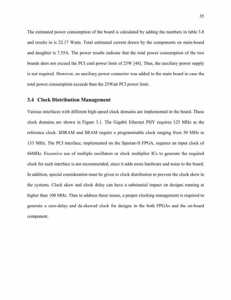
3.4 Clock Distribution Management Various interfaces with different high-speed clock domains are implemented in the board. These
clock domains are shown in Figure 3.1. The Gigabit Ethernet PHY requires 125 MHz as the
reference clock. SDRAM and SRAM require a programmable clock ranging from 50 MHz to
133 MHz. The PCI interface, implemented on the Spartan-II FPGA, requires an input clock of
66MHz. Excessive use of multiple oscillators or clock multiplier ICs to generate the required
clock for each interface is not recommended, since it adds more hardware and noise to the board.
In addition, special consideration must be given to clock distribution to prevent the clock skew in
the systems. Clock skew and clock delay can have a substantial impact on designs running at
higher than 100 MHz. Thus to address these issues, a proper clocking management is required to
generate a zero-delay and de-skewed clock for designs in the both FPGAs and the on-board
component.
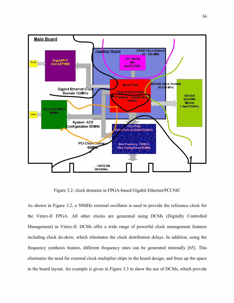
36
Figure 3.2: clock domains in FPGA-based Gigabit Ethernet/PCI NIC
As shown in Figure 3.2, a 50MHz external oscillator is used to provide the reference clock for
the Virtex-II FPGA. All other clocks are generated using DCMs (Digitally Controlled
Management) in Virtex-II. DCMs offer a wide range of powerful clock management features
including clock de-skew, which eliminates the clock distribution delays. In addition, using the
frequency synthesis feature, different frequency rates can be generated internally [65]. This
eliminates the need for external clock multiplier chips in the board design, and frees up the space
in the board layout. An example is given in Figure 3.3 to show the use of DCMs, which provide
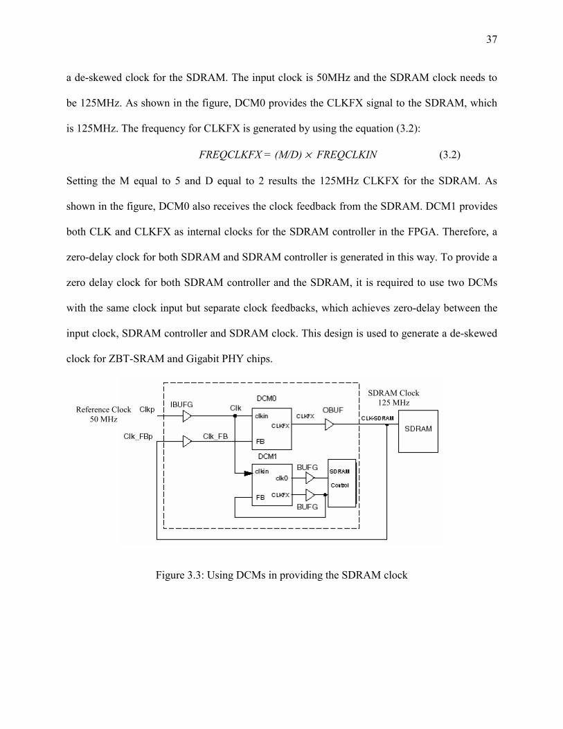
37
a de-skewed clock for the SDRAM. The input clock is 50MHz and the SDRAM clock needs to
be 125MHz. As shown in the figure, DCM0 provides the CLKFX signal to the SDRAM, which
is 125MHz. The frequency for CLKFX is generated by using the equation (3.2):
FREQCLKFX = (M/D) × FREQCLKIN (3.2)
Setting the M equal to 5 and D equal to 2 results the 125MHz CLKFX for the SDRAM. As
shown in the figure, DCM0 also receives the clock feedback from the SDRAM. DCM1 provides
both CLK and CLKFX as internal clocks for the SDRAM controller in the FPGA. Therefore, a
zero-delay clock for both SDRAM and SDRAM controller is generated in this way. To provide a
zero delay clock for both SDRAM controller and the SDRAM, it is required to use two DCMs
with the same clock input but separate clock feedbacks, which achieves zero-delay between the
input clock, SDRAM controller and SDRAM clock. This design is used to generate a de-skewed
clock for ZBT-SRAM and Gigabit PHY chips.
Figure 3.3: Using DCMs in providing the SDRAM clock
Reference Clock 50 MHz
SDRAM Clock 125 MHz
38
3.5 Layout Implementation The PC board is no longer just a means to hold ICs in place. At today’s high clock rates and fast
signal transitions, the PC board performs a vital function in feeding stable supply voltages to the
ICs and in maintaining signal integrity among the devices. Several issues should be considered in
the board layout design. Design techniques, which were used at slower frequencies (33 MHz and
lower) are no longer appropriate for these higher bus frequencies like 125MHz. More attention
must be paid to board layout, bus loading, and termination to ensure that short clock cycle times
can be met without noise, ringing, crosstalk or ground bounce.
In addition, it is required to design a proper power distribution system (PDS) [3]. Most
other large, dense ICs (such as large microprocessors) come with very specific bypass capacitor
requirements. The power supply demands for these devices are fixed and only fluctuate within a
certain range. The reason is that these devices are only designed to implement specific tasks in
their hard silicon. FPGAs do not share this property. FPGAs can implement a practically infinite
number of applications at undetermined frequencies and in multiple clock domains. Therefore, it
can be very complicated to predict what their transient current demands will be. Transient
current demands in digital devices are the cause of ground bounce, and the bane of high-speed
digital designs. In low-noise or high-power situations, the power supply decoupling network
must be tailored very closely to these transient current needs, otherwise ground bounce and
power supply noise will exceed the limits of the device.
To provide a power distribution system for the FPGAs, an approximate decoupling
network is designed to meet the FPGA current requirement per VCC pin. The Vcc in Virtex-II is
referred to FPGA power supplies: VCCINT (FPGA core voltage1.5v), VCCO (FPGA IO voltage
3.3V), and VCCAUX (FPGA auxiliary Voltage 3.3v). The generic approximately bypassing
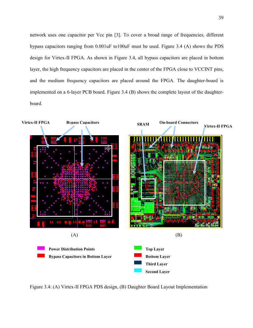
39
network uses one capacitor per Vcc pin [3]. To cover a broad range of frequencies, different
bypass capacitors ranging from 0.001uF to100uF must be used. Figure 3.4 (A) shows the PDS
design for Virtex-II FPGA. As shown in Figure 3.4, all bypass capacitors are placed in bottom
layer, the high frequency capacitors are placed in the center of the FPGA close to VCCINT pins,
and the medium frequency capacitors are placed around the FPGA. The daughter-board is
implemented on a 6-layer PCB board. Figure 3.4 (B) shows the complete layout of the daughter-
board.
Figure 3.4: (A) Virtex-II FPGA PDS design, (B) Daughter Board Layout Implementation
(B)
Top Layer
Bottom Layer
Third Layer
Second Layer
(A)
Bypass Capacitors in Bottom Layer
Power Distribution Points
Bypass Capacitors Virtex-II FPGA
Virtex-II FPGAOn-board Connectors SRAM
40
Virtex-II and SRAM are shown with white squares in the figure. To prevent reflections and
maintain signal integrity in high rate interfaces like PHY (125 MHz), Memory (125 MHz) and
PCI (66 MHz), output signals require proper termination. High pin count packages (especially
ball grid arrays) cannot accommodate external termination resistors. The use of DCI (Digitally
Controlled Impedance) feature in Virtex-II, which provides controlled impedance drivers and on-
chip termination, simplifies board layout design. This eliminates the need for external resistors,
and improves signal integrity in the NIC design.
During board layout, extra attention was paid to high-speed signal traces such as clock
signal, address traces and data paths. These traces must have constant impedance in each layer of
the board layout and must be properly terminated to avoid signal integrity. Adjacent traces must
be in perpendicular directions in order to avoid cross talk.
3.6 Avnet Board Compared to the FPGA-based NIC When we intended to send the board for fabrication, the Avnet Company released their Virtex-II
Pro Development Kit. This board is built around an extremely flexible FPGA-based development
platform, which includes two FPGAs, a 64-bit 33/66MHz PCI Connector, a Gigabit Ethernet
PHY and multiple memories. Figure 3.6 shows the Virtex-II PRO Development Kit picture. (In
this thesis, the board is called Avnet board). Although the Avnet board was not built to be a
functional NIC, since it was close enough to our design we decided to use this board to evaluate
the NIC controller design.
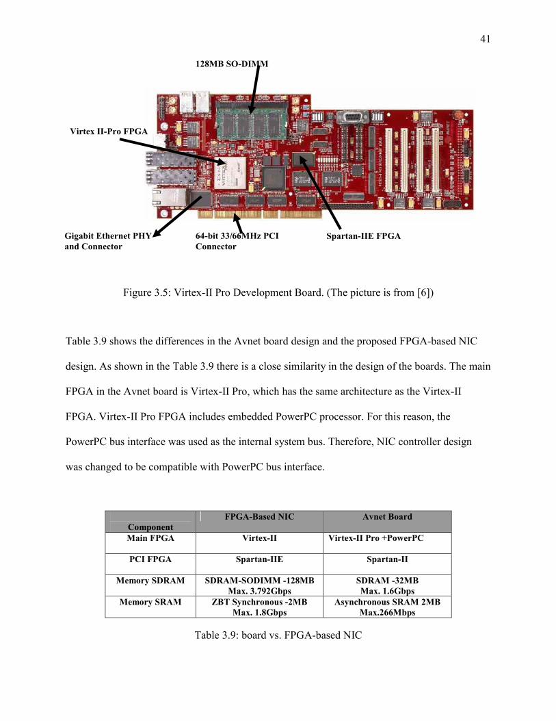
41
Figure 3.5: Virtex-II Pro Development Board. (The picture is from [6])
Table 3.9 shows the differences in the Avnet board design and the proposed FPGA-based NIC
design. As shown in the Table 3.9 there is a close similarity in the design of the boards. The main
FPGA in the Avnet board is Virtex-II Pro, which has the same architecture as the Virtex-II
FPGA. Virtex-II Pro FPGA includes embedded PowerPC processor. For this reason, the
PowerPC bus interface was used as the internal system bus. Therefore, NIC controller design
was changed to be compatible with PowerPC bus interface.
Component
FPGA-Based NIC Avnet Board
Main FPGA Virtex-II Virtex-II Pro +PowerPC
PCI FPGA
Spartan-IIE Spartan-II
Memory SDRAM SDRAM-SODIMM -128MB Max. 3.792Gbps
SDRAM -32MB Max. 1.6Gbps
Memory SRAM ZBT Synchronous -2MB Max. 1.8Gbps
Asynchronous SRAM 2MB Max.266Mbps
Table 3.9: board vs. FPGA-based NIC
64-bit 33/66MHz PCI Connector
Gigabit Ethernet PHY and Connector
Spartan-IIE FPGA
128MB SO-DIMM
Virtex II-Pro FPGA
42
The on-board SDRAM has maximum data width of 32-bits, and access latency of 8 cycles. The
Table 3.10 shows the maximum throughput based on these characteristics.
Burst Length Transfer
cycles Number of bits per
Transfer Max Practical Bandwidth
(Mbps) Burst-1 8 32 400
Burst-2 10 32x 2 640
Burst-4 12 32 x 4 1066.6
Burst-8 16 32x 8 1600
Table 3.10: Maximum bandwidth with the SDRAM on Avnet board
The SRAM on the Avnet board is asynchronous which is slower than the synchronous SRAMs,
if no overlapped memory operation is considered. The access time latency in the Cypress
asynchronous SRAM is 12ns operating at 80MHz frequency [30]. Therefore, the maximum
bandwidth can not exceed than 266.6Mbps. The next chapter investigates the design space for
efficient architectures in the NIC controller to meet the throughput and latency performance
requirements.
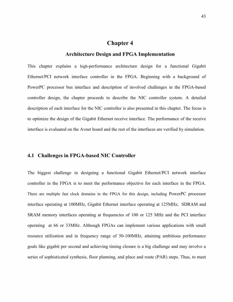
43
4 Chapter 4
Architecture Design and FPGA Implementation This chapter explains a high-performance architecture design for a functional Gigabit
Ethernet/PCI network interface controller in the FPGA. Beginning with a background of
PowerPC processor bus interface and description of involved challenges in the FPGA-based
controller design, the chapter proceeds to describe the NIC controller system. A detailed
description of each interface for the NIC controller is also presented in this chapter. The focus is
to optimize the design of the Gigabit Ethernet receive interface. The performance of the receive
interface is evaluated on the Avnet board and the rest of the interfaces are verified by simulation.
4.1 Challenges in FPGA-based NIC Controller
The biggest challenge in designing a functional Gigabit Ethernet/PCI network interface
controller in the FPGA is to meet the performance objective for each interface in the FPGA.
There are multiple fast clock domains in the FPGA for this design, including PowerPC processor
interface operating at 100MHz, Gigabit Ethernet interface operating at 125MHz, SDRAM and
SRAM memory interfaces operating at frequencies of 100 or 125 MHz and the PCI interface
operating at 66 or 33MHz. Although FPGAs can implement various applications with small
resource utilization and in frequency range of 50-100MHz, attaining ambitious performance
goals like gigabit per second and achieving timing closure is a big challenge and may involve a
series of sophisticated synthesis, floor planning, and place and route (PAR) steps. Thus, to meet
44
the performance objective in such a high speed/high density application, a proven methodology
for timing closure is required.
Another challenge to meet the performance objective in the Gigabit Ethernet/PCI NIC
proposed in this thesis is access latency in SDRAMs. As mentioned earlier, current NICs use
SRAMs, which are faster memories instead of SDRAMs. Although SDRAMs provide larger
memory capacity, their access latency is an important issue in over all system performance.
DRAM memories due to their 3-D structure (bank, row, and column) should follow a sequence
of operations for each memory reference. These operations include bank precharge, row
activation, and column access, which increase access latency for each memory reference.
However, the bandwidth and latency of a memory system are strongly dependent on the manner
in which accesses interact with the structure of banks, rows, and columns characteristic of
contemporary DRAM chips. A well-designed memory controller can schedule to access several
columns of memory within one row access in the SDRAM, which results in increased bandwidth
and overall system performance [57].
4.2 PowerPC Bus Interface Overview Figure 4.1 shows a top-level block diagram of PowerPC processor and its bus interface. The
PowerPC 405 processor is a 32-bit implementation of the IBM PowerPC™ RISC processor [85].
The Virtex-II Pro FPGA (XC2VP20) on the Avnet board has two hard-core PowerPC processors.
Each processor runs at 300+ MHz and 420 Dhrystone MIPS [66]. The PowerPC processor is
supported by IBM CoreConnect™ technology, a high-bandwidth 64-bit bus architecture that
runs at 100 to 133 MHz [71]. The CoreConnect architecture is implemented as a soft IP within
45
the Virtex-II Pro FPGA fabric. The CoreConnect bus architecture has two main buses, called the
Processor Local Bus (PLB) and the On-chip Peripheral Bus (OPB).
Figure 4.1 : PowerPC bus interface block diagram (modified from [86])
The PowerPC405 core accesses high speed and high performance system resources through the
PLB. The PLB bus provides separate 32-bit address and 64-bit data buses for the instruction and
data sides. The PLB, provided by Xilinx, can operate up to 100MHz. The peak data rate transfers
can go up to 6.4Mbps. The PLB arbiter handles bus arbitration and the movement of data and
control signals between masters and slaves. The processor clock and PLB must be run at an
integer ratio 1:1 …16:1. As an example, the processor block can operate at 300 MHz whereas the
PLB operates at 100 MHz [85].
The OPB is the secondary I/O bus protocol and is intended for less complex, lower
performance peripherals. The OPB, provided by Xilinx, has a shared 32-bit address bus and a
PowerPC Processor
BRAM
PLB-to-OPBBridge
PLB-Bus
OPB-Bus
PLB Arbiter
OPB Arbiter
OPB-Master OPB-Slave
46
shared 32-bit data bus and it can support 16 masters and slaves. The OPB clock can go up to 100
MHz and the peak data rate transfers is 3.2Gbps. The OPB arbiter receives bus requests from
OPB masters and grants the bus to one of them [85].
As shown in Figure 4.1, the processor core can access the slave peripherals on this bus
through the PLB-to-OPB-Bridge unit. The PLB-to-OPB-Bridge translates PLB transactions into
OPB transactions. It functions as a slave on the PLB side and as a master on the OPB side. The
bridge is necessary in systems where a PLB master device, such as a CPU, requires access to
OPB peripherals. The PLB CLK and the OPB CLK must be positive-edge aligned. All OPB
transactions are synchronous with the PLB. The PLB bus and the OPB bus must be run at an
integer ratio: 1:1… 4:1.As an example, the PLB bus operates at 100 MHz when the OPB bus
operates at 50- MHz.
4.2.1 OPB interfaces The OPB buse is composed of masters, slaves, a bus interconnect, and an arbiter. Peripherals are
connected to the OPB bus as masters and/or slaves. The OPB arbiter arbitrates the bus ownership
between masters. Figure 4.3, shows the OPB masters, slaves, arbiter and their main control
signals. In Xilinx FPGAs, the OPB is implemented as a simple OR structure. The OPB bus
signals are created by logically OR’ing the signals that drive the bus. OPB devices that are not
active during a transaction are required to drive zeros into the OR structure. Bus arbitration
signals such as M-Request and OPB-MGrant are directly connected between the OPB arbiter and
each OPB master device. The OPB_V20, which is used in this implementation supports up to 16
masters and an unlimited number of slaves [85].
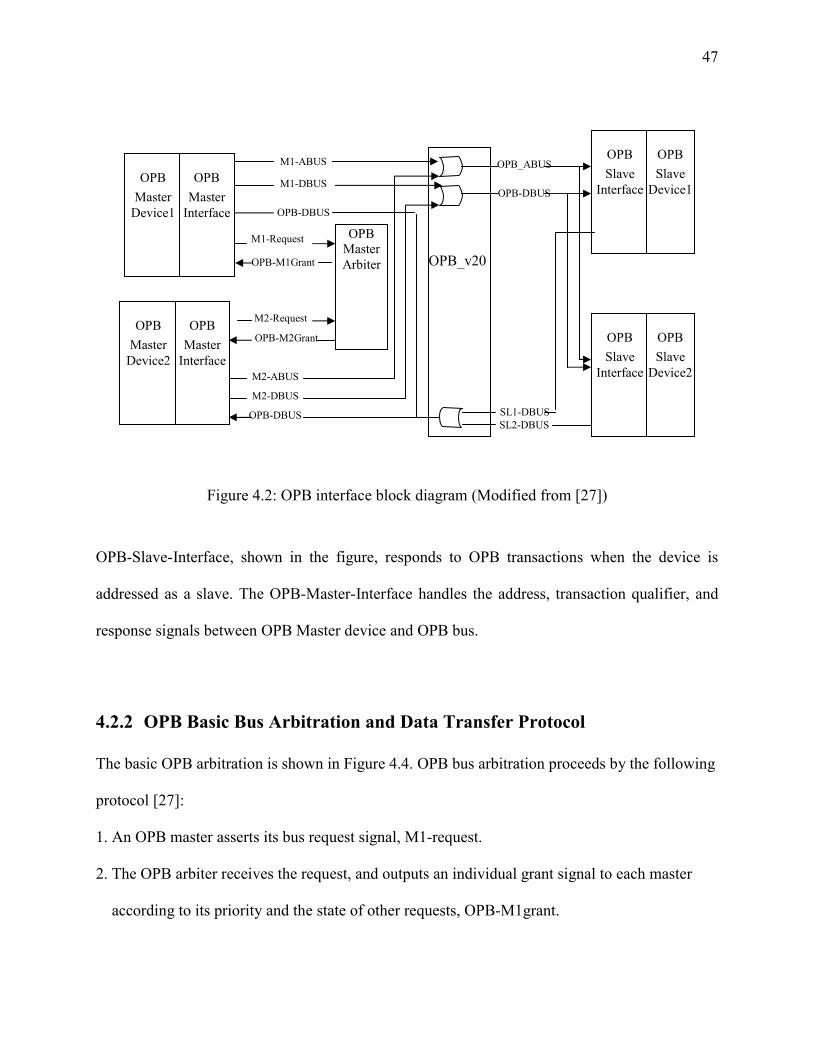
47
Figure 4.2: OPB interface block diagram (Modified from [27])
OPB-Slave-Interface, shown in the figure, responds to OPB transactions when the device is
addressed as a slave. The OPB-Master-Interface handles the address, transaction qualifier, and
response signals between OPB Master device and OPB bus.
4.2.2 OPB Basic Bus Arbitration and Data Transfer Protocol The basic OPB arbitration is shown in Figure 4.4. OPB bus arbitration proceeds by the following
protocol [27]:
1. An OPB master asserts its bus request signal, M1-request.
2. The OPB arbiter receives the request, and outputs an individual grant signal to each master
according to its priority and the state of other requests, OPB-M1grant.
OPB_v20
OPB Slave
Interface
M1-ABUS
M1-DBUS
M1-Request
OPB-M1Grant
M2-Request
OPB-M2Grant
M2-ABUS
M2-DBUS
OPB-DBUS
OPB-DBUS
OPB_ABUS
OPB-DBUS
SL1-DBUS SL2-DBUS
OPB Master Arbiter
OPB Slave
Device1
OPB Slave
Interface
OPB Slave
Device2
OPB Master
Device1
OPB Master
Interface
OPB Master
Device2
OPB Master
Interface
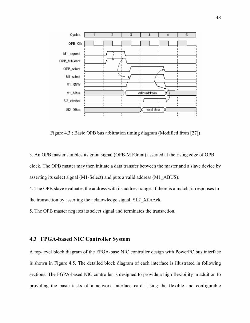
48
Figure 4.3 : Basic OPB bus arbitration timing diagram (Modified from [27])
3. An OPB master samples its grant signal (OPB-M1Grant) asserted at the rising edge of OPB
clock. The OPB master may then initiate a data transfer between the master and a slave device by
asserting its select signal (M1-Select) and puts a valid address (M1_ABUS).
4. The OPB slave evaluates the address with its address range. If there is a match, it responses to
the transaction by asserting the acknowledge signal, SL2_XferAck.
5. The OPB master negates its select signal and terminates the transaction.
4.3 FPGA-based NIC Controller System A top-level block diagram of the FPGA-base NIC controller design with PowerPC bus interface
is shown in Figure 4.5. The detailed block diagram of each interface is illustrated in following
sections. The FGPA-based NIC controller is designed to provide a high flexibility in addition to
providing the basic tasks of a network interface card. Using the flexible and configurable
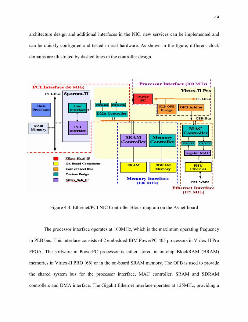
49
architecture design and additional interfaces in the NIC, new services can be implemented and
can be quickly configured and tested in real hardware. As shown in the figure, different clock
domains are illustrated by dashed lines in the controller design.
Figure 4.4: Ethernet/PCI NIC Controller Block diagram on the Avnet-board
The processor interface operates at 100MHz, which is the maximum operating frequency
in PLB bus. This interface consists of 2 embedded IBM PowerPC 405 processors in Virtex-II Pro
FPGA. The software in PowerPC processor is either stored in on-chip BlockRAM (BRAM)
memories in Virtex-II PRO [66] or in the on-board SRAM memory. The OPB is used to provide
the shared system bus for the processor interface, MAC controller, SRAM and SDRAM
controllers and DMA interface. The Gigabit Ethernet interface operates at 125MHz, providing a
50
2Gbps bidirectional full duplex or 1Gbps half-duplex throughput. The main blocks in this
interface include MAC controller, FIFO-RX and FIFO-TX, and a Gigabit MAC Core. Since the
functionality of the Gigabit MAC is fixed, this controller uses Gigabit Ethernet MAC Core
offered by Xilinx to interface with the on-board PHY chip. The MAC controller is a state
machine, which manages packets transfer operation between FIFOs and OPB bus. FIFO-RX and
FIFO-TX with asynchronous clocks are used to provide data synchronization and buffering
between the MAC Controller operating at 100MHz and Gigabit MAC core operating at 125MHz.
The memory controller provides a 32-bit high-speed memory bus for the on-board
SDRAM memory. Various implementations for the memory controller interface are investigated
in this chapter. The first design considers single transfers to the SDRAM, whereas the second
design improves the memory controller and OPB-slave interface to provide burst transfers to the
SDRAM. The memory controller with this design is implemented for 100 or 125 MHz operation.
The 100MHz implementation is synchronous with OPB bus frequency and has a simpler
architecture whereas 125MHz implementation requires DCMS and synchronizing interfaces to
provide higher frequency than OPB bus frequency. The architecture for this design is more
complex but provides faster read and write accesses to the SDRAM.
The PCI interface operates at 66 or 33MHz with 64-bit data or 32-bit width data bus at
the PCI connector. The main blocks for this interface in Virtex-II Pro FPGA are DMA controller,
FIFO-RD and FIFO-WR. The DMA controller provides the DMA transfers from FIFOs to the
OPB bus and operates at 100MHz. FIFO-RD and FIFO-WR with asynchronous clocks are used
to provide data synchronization and buffering between the PCI interface in Spartan-II and DMA
controller in Virtex-II Pro. As mentioned earlier, since PCI protocol functionality is fixed and
well-defined the Xilinx PCI core is used to provide the interface at PCI connector. The PCI core
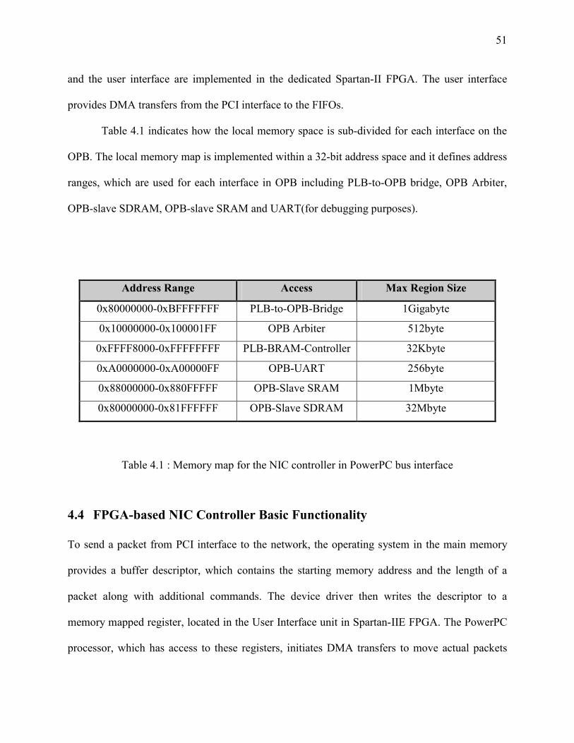
51
and the user interface are implemented in the dedicated Spartan-II FPGA. The user interface
provides DMA transfers from the PCI interface to the FIFOs.
Table 4.1 indicates how the local memory space is sub-divided for each interface on the
OPB. The local memory map is implemented within a 32-bit address space and it defines address
ranges, which are used for each interface in OPB including PLB-to-OPB bridge, OPB Arbiter,
OPB-slave SDRAM, OPB-slave SRAM and UART(for debugging purposes).
Address Range Access Max Region Size
0x80000000-0xBFFFFFFF PLB-to-OPB-Bridge 1Gigabyte
0x10000000-0x100001FF OPB Arbiter 512byte
0xFFFF8000-0xFFFFFFFF PLB-BRAM-Controller 32Kbyte
0xA0000000-0xA00000FF OPB-UART 256byte
0x88000000-0x880FFFFF OPB-Slave SRAM 1Mbyte
0x80000000-0x81FFFFFF OPB-Slave SDRAM 32Mbyte
Table 4.1 : Memory map for the NIC controller in PowerPC bus interface
4.4 FPGA-based NIC Controller Basic Functionality To send a packet from PCI interface to the network, the operating system in the main memory
provides a buffer descriptor, which contains the starting memory address and the length of a
packet along with additional commands. The device driver then writes the descriptor to a
memory mapped register, located in the User Interface unit in Spartan-IIE FPGA. The PowerPC
processor, which has access to these registers, initiates DMA transfers to move actual packets
52
from the main memory to the FIFO-WR in the Virtex-II Pro FPGA. Once the packets are
received, they will be moved to the SDRAM using address and length information in buffer
descriptor. The MAC controller sends the packets to the FIFO-TX and informs the Gigabit MAC
Core to start transmitting packets to the PHY Ethernet chip. Once the packets are sent to the
network, the NIC informs the device driver.
At Ethernet interface, when packets are received by the on-board PHY, the Gigabit MAC
Core stores them in the FIFO-RX. The MAC controller reads the received packets from the
FIFO-RX and stores them in the memory through the OPB Bus transaction. The memory
controller provides interface between the local memory on the NIC and the OPB bus
transactions. Once the packets are stored in the SDRAM memory, the DMA controller transfers
the packets to the main memory through the PCI BUS.
4.5 Gigabit Ethernet Receiver Interface The Gigabit Ethernet receive interface is responsible for accepting packets from the external
network interface and storing them in the local memory (SDRAM) along with an associated
receive descriptor. A top-level block diagram of the Gigabit Ethernet receiver interface is shown
in Figure 4.6. The flow for receiving packets is the same as the flow described in section 4.5. All
data, which is received from the Ethernet interface goes through synchronizing FIFOs. As shown
in the figure, all design parts in Gigabit Ethernet interface domain operate at 125 MHz whereas
design parts in OPB bus interface operate at 100 MHz. The SDRAM controller operates with
programmable clock of 100 and 125MHz generated by the Clock Generator unit.
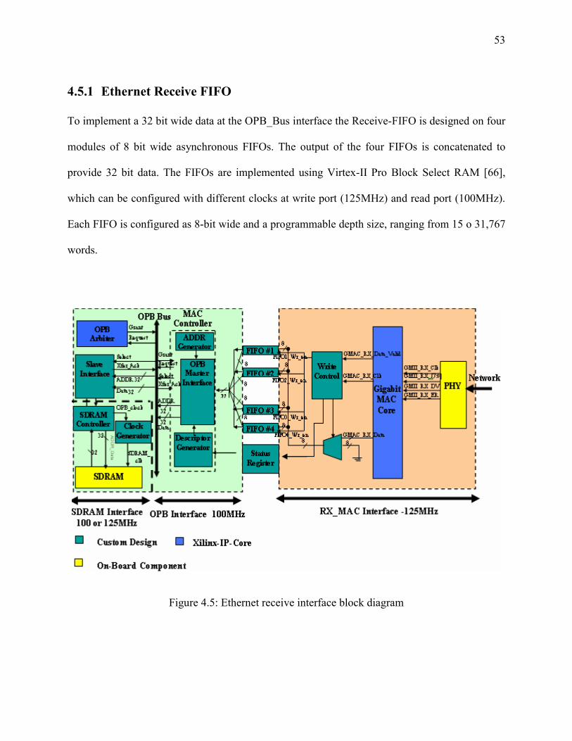
53
4.5.1 Ethernet Receive FIFO To implement a 32 bit wide data at the OPB_Bus interface the Receive-FIFO is designed on four
modules of 8 bit wide asynchronous FIFOs. The output of the four FIFOs is concatenated to
provide 32 bit data. The FIFOs are implemented using Virtex-II Pro Block Select RAM [66],
which can be configured with different clocks at write port (125MHz) and read port (100MHz).
Each FIFO is configured as 8-bit wide and a programmable depth size, ranging from 15 o 31,767
words.
Figure 4.5: Ethernet receive interface block diagram
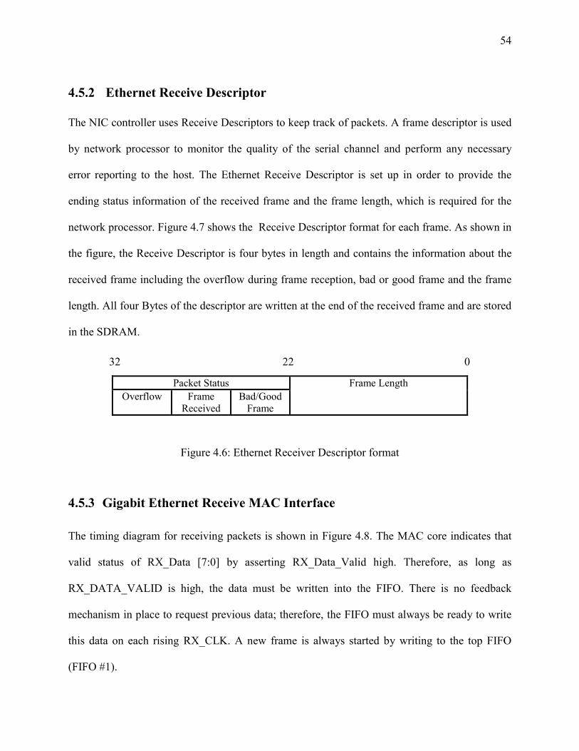
54
4.5.2 Ethernet Receive Descriptor The NIC controller uses Receive Descriptors to keep track of packets. A frame descriptor is used
by network processor to monitor the quality of the serial channel and perform any necessary
error reporting to the host. The Ethernet Receive Descriptor is set up in order to provide the
ending status information of the received frame and the frame length, which is required for the
network processor. Figure 4.7 shows the Receive Descriptor format for each frame. As shown in
the figure, the Receive Descriptor is four bytes in length and contains the information about the
received frame including the overflow during frame reception, bad or good frame and the frame
length. All four Bytes of the descriptor are written at the end of the received frame and are stored
in the SDRAM.
Packet Status Overflow Frame
Received Bad/Good
Frame
Frame Length
Figure 4.6: Ethernet Receiver Descriptor format
4.5.3 Gigabit Ethernet Receive MAC Interface
The timing diagram for receiving packets is shown in Figure 4.8. The MAC core indicates that
valid status of RX_Data [7:0] by asserting RX_Data_Valid high. Therefore, as long as
RX_DATA_VALID is high, the data must be written into the FIFO. There is no feedback
mechanism in place to request previous data; therefore, the FIFO must always be ready to write
this data on each rising RX_CLK. A new frame is always started by writing to the top FIFO
(FIFO #1).
32 22 0
55
Figure 4.7: Timing diagram of receiving data in Gigabit Ethernet interface (Modified from [79]).
The next 8-bit word of data from the MAC is written into the FIFO #2, then FIFO #3 and FIFO
#4 and this repeats until the end of frame, which is indicated by RX_DATA_VALID going low.
Write-Control state machine, shown in Figure 4.6, handles generating Wr_En signal in this way.
To align the last data in the four FIFOs, the Write-Control unit generates correct numbers of
Wr_EN signal for the rest of FIFOs, which were not written after frame was finished. This
ensures that the start of the next frame will be written to the FIFO#1 and the sequence can
continue. The end of frame is indicated by the RX_GOOD_FRAME or RX_BAD_FRAME
signals from the MAC core, which is used in Receive Descriptor.
4.5.4 MAC Controller Design with Single Transfer The MAC Controller, shown in Figure 4.6, consists of ADDR generator, OPB-master interface
and Descriptor generator units. The OPB-master interface translates the master device
transaction into a corresponding OPB master transaction. In this section, two designs of OPB-
master interface are explored for the MAC-controller.
56
4.5.5 MAC Controller Design with Xilinx OPB Master Core The first implementation of the MAC controller is performed by using OPB-master core
provided by Xilinx, called OPB-IPIF master attachment [68]. IPIF stands for Intellectual
Property Interface and the OPB IPIF master attachment is a standardized interface module for
connecting custom designed master devices (here MAC controller) to the IBM On-Chip
Peripheral Bus (OPB). Figure 4.9 shows a top-level block diagram of Xilinx OPB-IPIF master
attachment. The IP Core and service blocks shown in the IPIF figure use a set of signals and
protocols called the IP Interconnect (or IPIC).
Figure 4.8: Xilinx OPB-IPIF master attachment top-level block diagram (From [68])
The Master Attachment translates the IP Interconnect master transaction into a corresponding
OPB master transaction. As OPB transfers complete, the Master Attachment generates the IPIC
response signals. As shown in the figure, the Xilinx OPB-master is designed to be extremely
flexible for different applications. However, as timing analysis results by ModelSim and Logic
57
Analyze indicated, the first version of this core which was the only available OPB-IPIF master
core by Xilinx was not designed for a high performance implementation. Timing analysis by
Modelsim indicated that there is 7 cycles latency in Xilinx OPB-master core to assert the select
signal for OPB transfers; this is discussed in detail in Section 5.3.5.
4.5.6 MAC Controller Design with Optimized Custom-designed OPB-Master The HDL code of the Xilinx OPB-master core is not available to investigate the reason for this
latency in detail. However, it seems that the RTL coding for the Xilinx OPB-master core was not
efficient to enhance performance. More over, timing analysis results from Xilinx Timing
Analyzer tool [81] indicate that the critical paths in the Xilinx OPB-master core design can not
fit within 10ns requirement provide by OPB clock. Unfortunately, the HDL code of the Xilinx
OPB-master core is not available, so it is not possible to improve its performance. The custom-
designed OPB-master provides simpler architecture and decreases the slice counts by 75%
compared to Xilinx OPB-master core. Moreover, it is designed by applying efficient RTL coding
styles, which is described in next section to enhance speed through reducing logic levels and
complexity in the state machines.
4.5.7 Achieving Timing Closure A noticeable difference in ASICs and FPGA is that ASIC architectures have the ability to
tolerate a wide range of RTL coding styles while still allowing designers to meet their design
goals. However, FPGA architectures are more sensitive to coding styles and design practices In
many cases, slight modifications in coding practices can improve the system performance
anywhere from 10% to 100% [73]. A logic level in a FPGA is considered one Combinatorial
58
Logic Block (CLB) delay. If the amount of logic that can fit into one CLB is exceeded, another
level of logic delay is added which results in increased delay. For example, a module with 6 to 8
FPGA logic levels would operate at ~50MHz where as a module with 4 to 6 FPGA logic levels
would operate at ~100MHz.
This section provides the coding techniques, which are applied in the NIC controller architecture
design specifically in the OPB-master interface design. These techniques include duplicating
register to decrease the fanouts, using one-hot state machines to decrease the logic complexity
for each state, adding pipeline stages to break up long data paths in multiple clocks and using
case statements instead of else-if statements to enhance the speed of multiplexing. As mentioned
in last section the critical paths in the first version of Xilinx OPB-master core could not fit within
10 ns OPB clock. To work around these problems, an approximate amount of logic levels should
be considered. The placement of the logic should be taken into consideration, too. Some of the
techniques that are used to decrease the logic levels and enhance the performance of the design
are discussed as the following:
Duplicating Registers
Since FPGA architectures are plentiful with registers, duplicating the number of registers in a
critical path, which contains a large number of loads, is very useful. This technique reduces the
fanout of the critical path, which substantially improves the system performance. An example is
given in Figure 4.10 and 4.11 to show how using register duplication can reduce the fanout.
Figure 4.10 shows the memory address (Mem-ADDR-In [31:0]) and the address enable signal
(Tri-Addr-En) in MAC controller and SDRAM controller interface. As shown in the figure, the
enable signal is generated from a single register so there is a 32 fanout for this register.
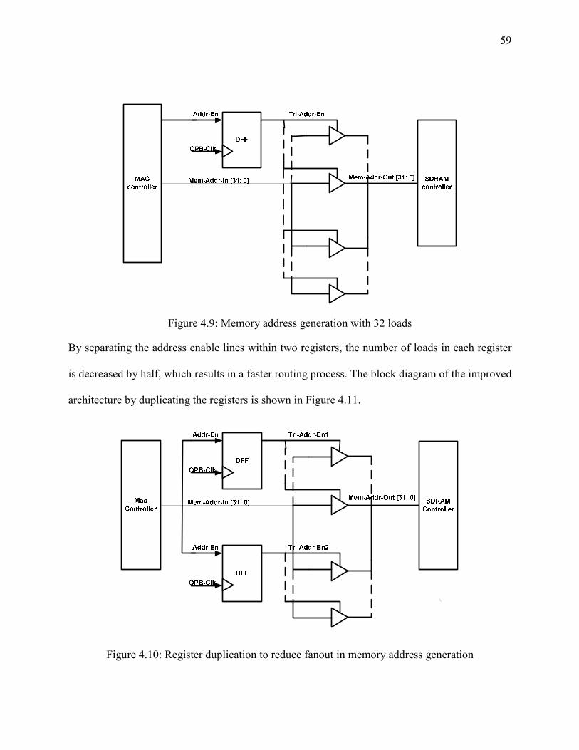
59
Figure 4.9: Memory address generation with 32 loads
By separating the address enable lines within two registers, the number of loads in each register
is decreased by half, which results in a faster routing process. The block diagram of the improved
architecture by duplicating the registers is shown in Figure 4.11.
Figure 4.10: Register duplication to reduce fanout in memory address generation
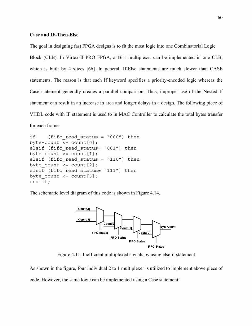
60
Case and IF-Then-Else
The goal in designing fast FPGA designs is to fit the most logic into one Combinatorial Logic
Block (CLB). In Virtex-II PRO FPGA, a 16:1 multiplexer can be implemented in one CLB,
which is built by 4 slices [66]. In general, If-Else statements are much slower than CASE
statements. The reason is that each If keyword specifies a priority-encoded logic whereas the
Case statement generally creates a parallel comparison. Thus, improper use of the Nested If
statement can result in an increase in area and longer delays in a design. The following piece of
VHDL code with IF statement is used to in MAC Controller to calculate the total bytes transfer
for each frame:
if (fifo_read_status = “000”) thenbyte-count <= count[0];elsif (fifo_read_status= “001”) thenbyte_count <= count[1];elsif (fifo_read_status = “110”) thenbyte_count <= count[2];elsif (fifo_read_status= “111”) thenbyte_count <= count[3];end if;
The schematic level diagram of this code is shown in Figure 4.14.
Figure 4.11: Inefficient multiplexed signals by using else-if statement
As shown in the figure, four individual 2 to 1 multiplexer is utilized to implement above piece of
code. However, the same logic can be implemented using a Case statement:
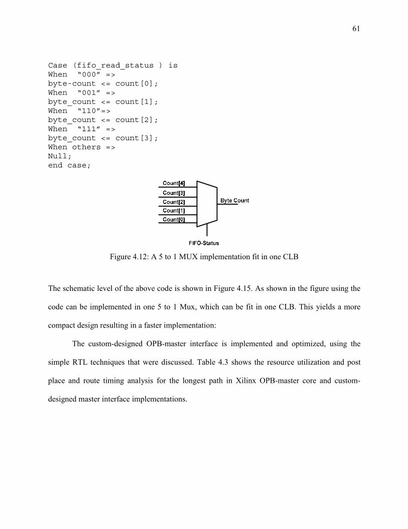
61
Case (fifo_read_status ) isWhen “000” =>byte-count <= count[0];When “001” =>byte_count <= count[1];When “110”=>byte_count <= count[2];When “111” =>byte_count <= count[3];When others =>Null;end case;
Figure 4.12: A 5 to 1 MUX implementation fit in one CLB
The schematic level of the above code is shown in Figure 4.15. As shown in the figure using the
code can be implemented in one 5 to 1 Mux, which can be fit in one CLB. This yields a more
compact design resulting in a faster implementation:
The custom-designed OPB-master interface is implemented and optimized, using the
simple RTL techniques that were discussed. Table 4.3 shows the resource utilization and post
place and route timing analysis for the longest path in Xilinx OPB-master core and custom-
designed master interface implementations.
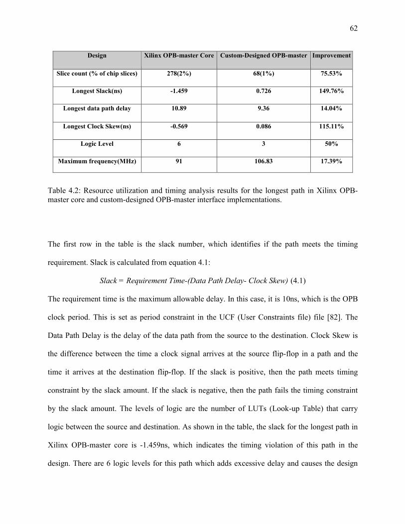
62
Design Xilinx OPB-master Core Custom-Designed OPB-master Improvement
Slice count (% of chip slices) 278(2%) 68(1%) 75.53%
Longest Slack(ns) -1.459 0.726 149.76%
Longest data path delay 10.89 9.36 14.04%
Longest Clock Skew(ns) -0.569 0.086 115.11%
Logic Level 6 3 50%
Maximum frequency(MHz) 91 106.83 17.39%
Table 4.2: Resource utilization and timing analysis results for the longest path in Xilinx OPB-master core and custom-designed OPB-master interface implementations.
The first row in the table is the slack number, which identifies if the path meets the timing
requirement. Slack is calculated from equation 4.1:
Slack = Requirement Time-(Data Path Delay- Clock Skew) (4.1)
The requirement time is the maximum allowable delay. In this case, it is 10ns, which is the OPB
clock period. This is set as period constraint in the UCF (User Constraints file) file [82]. The
Data Path Delay is the delay of the data path from the source to the destination. Clock Skew is
the difference between the time a clock signal arrives at the source flip-flop in a path and the
time it arrives at the destination flip-flop. If the slack is positive, then the path meets timing
constraint by the slack amount. If the slack is negative, then the path fails the timing constraint
by the slack amount. The levels of logic are the number of LUTs (Look-up Table) that carry
logic between the source and destination. As shown in the table, the slack for the longest path in
Xilinx OPB-master core is -1.459ns, which indicates the timing violation of this path in the
design. There are 6 logic levels for this path which adds excessive delay and causes the design
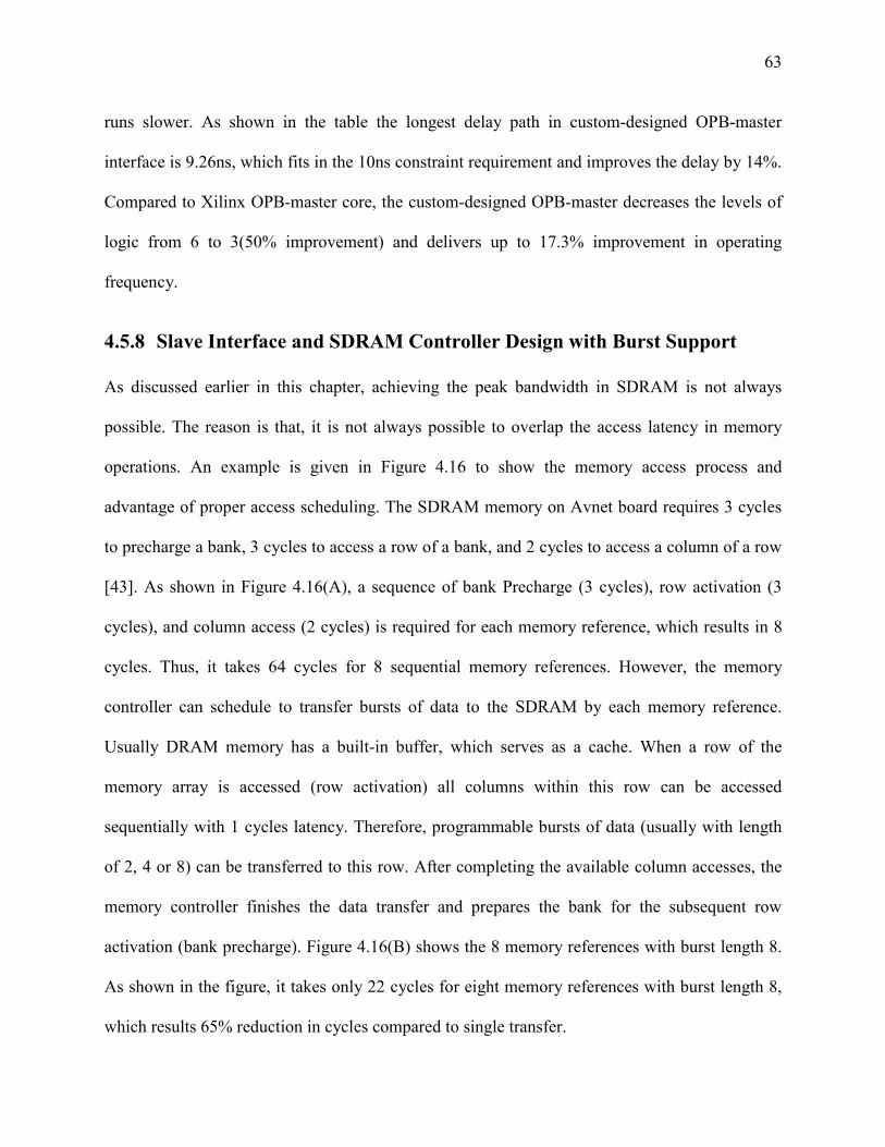
63
runs slower. As shown in the table the longest delay path in custom-designed OPB-master
interface is 9.26ns, which fits in the 10ns constraint requirement and improves the delay by 14%.
Compared to Xilinx OPB-master core, the custom-designed OPB-master decreases the levels of
logic from 6 to 3(50% improvement) and delivers up to 17.3% improvement in operating
frequency.
4.5.8 Slave Interface and SDRAM Controller Design with Burst Support As discussed earlier in this chapter, achieving the peak bandwidth in SDRAM is not always
possible. The reason is that, it is not always possible to overlap the access latency in memory
operations. An example is given in Figure 4.16 to show the memory access process and
advantage of proper access scheduling. The SDRAM memory on Avnet board requires 3 cycles
to precharge a bank, 3 cycles to access a row of a bank, and 2 cycles to access a column of a row
[43]. As shown in Figure 4.16(A), a sequence of bank Precharge (3 cycles), row activation (3
cycles), and column access (2 cycles) is required for each memory reference, which results in 8
cycles. Thus, it takes 64 cycles for 8 sequential memory references. However, the memory
controller can schedule to transfer bursts of data to the SDRAM by each memory reference.
Usually DRAM memory has a built-in buffer, which serves as a cache. When a row of the
memory array is accessed (row activation) all columns within this row can be accessed
sequentially with 1 cycles latency. Therefore, programmable bursts of data (usually with length
of 2, 4 or 8) can be transferred to this row. After completing the available column accesses, the
memory controller finishes the data transfer and prepares the bank for the subsequent row
activation (bank precharge). Figure 4.16(B) shows the 8 memory references with burst length 8.
As shown in the figure, it takes only 22 cycles for eight memory references with burst length 8,
which results 65% reduction in cycles compared to single transfer.
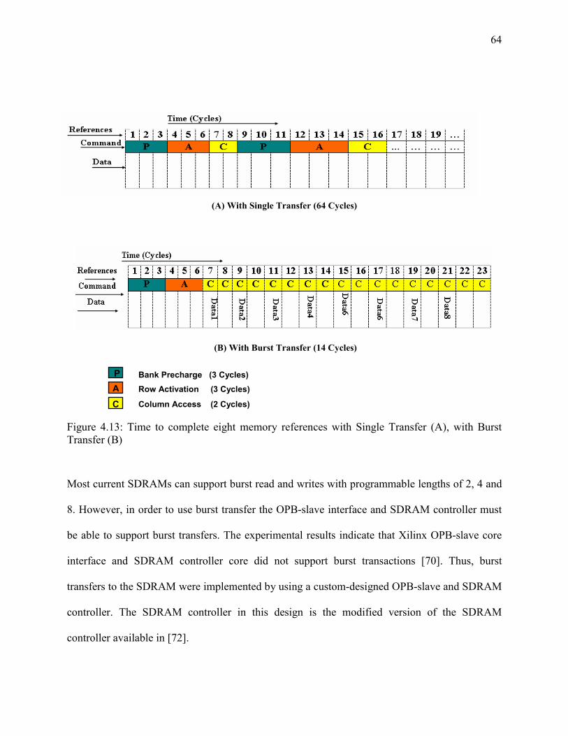
64
(A) With Single Transfer (64 Cycles)
(B) With Burst Transfer (14 Cycles)
Figure 4.13: Time to complete eight memory references with Single Transfer (A), with Burst Transfer (B)
Most current SDRAMs can support burst read and writes with programmable lengths of 2, 4 and
8. However, in order to use burst transfer the OPB-slave interface and SDRAM controller must
be able to support burst transfers. The experimental results indicate that Xilinx OPB-slave core
interface and SDRAM controller core did not support burst transactions [70]. Thus, burst
transfers to the SDRAM were implemented by using a custom-designed OPB-slave and SDRAM
controller. The SDRAM controller in this design is the modified version of the SDRAM
controller available in [72].
P A C
Bank Precharge (3 Cycles) Row Activation (3 Cycles)
Column Access (2 Cycles)
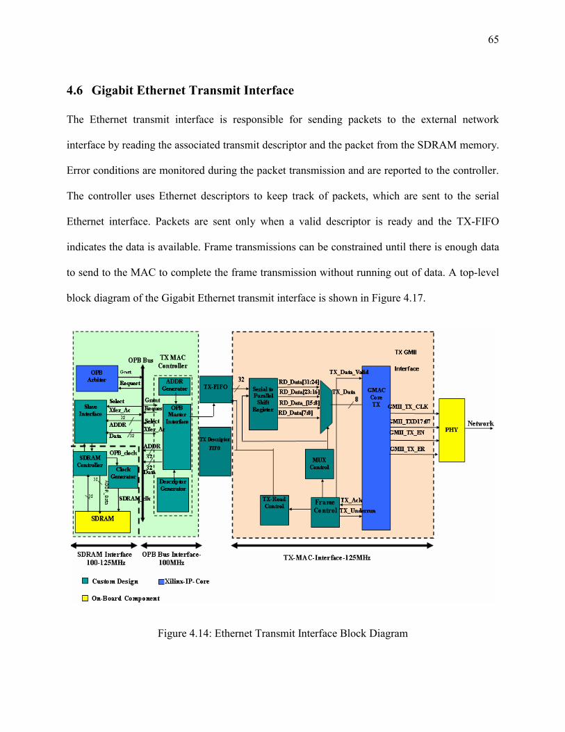
65
4.6 Gigabit Ethernet Transmit Interface The Ethernet transmit interface is responsible for sending packets to the external network
interface by reading the associated transmit descriptor and the packet from the SDRAM memory.
Error conditions are monitored during the packet transmission and are reported to the controller.
The controller uses Ethernet descriptors to keep track of packets, which are sent to the serial
Ethernet interface. Packets are sent only when a valid descriptor is ready and the TX-FIFO
indicates the data is available. Frame transmissions can be constrained until there is enough data
to send to the MAC to complete the frame transmission without running out of data. A top-level
block diagram of the Gigabit Ethernet transmit interface is shown in Figure 4.17.
Figure 4.14: Ethernet Transmit Interface Block Diagram
66
As shown in the figure, the architecture design for transmitter interface is very similar to the
design of the receive interface. The TX-MAC Controller unit is a state machine, which controls
data transfers from OPB bus to TX-FIFO. The OPB-master interface provides interface between
OPB bus and TX-MAC-Controller unit. To ensure that the transmitter does not run out of data,
during sending data to the to the MAC in the middle of a frame (underrun), the start of frame
transmission to the MAC is constrained until there is at least one complete frame stored in the
TX-FIFO. The order in which data is written into the TX-FIFO is the order in which it is read
out. The TX-FIFO with asynchronous clocks is used to provide data synchronization and
buffering between TX-MAC Controller operating at 100MHz and TX-Gigabit MAC core
operating at 125MHz. The TX-FIFO is implemented using Virtex-II Pro Block Select RAM that
has different clocks for read and write ports [66].
The TX-Descriptor-FIFO contains Ethernet transmitter descriptors, which are set up by
the network processor to indicate the status of transmit packets. Like TX-FIFO, the TX-
Descriptor FIFO is implemented using Virtex-II Pro Block Select RAMs and is configured as 32
bit wide and the depth size of 15 words.
The Serial-to-Parallel-Shift register unit divides the 32-bit width data to 8-bit data width
for Gigabit MAC Core. As shown in the figure, the select signal for multiplexing the 8-bit data is
determined by MUX-Control unit. The Frame-Control unit generates control signals for MUX-
Control and TX-Read-control, depending on the status of TX-ACK and TX-Underrun from TX-
Gigabit MAC Core.
4.7 PCI Interface As mentioned earlier, the PCI core and PCI User Interface are implemented on Spartan-IIE
FPGA. There are a few design issues in PCI Interface, which are briefly described here.
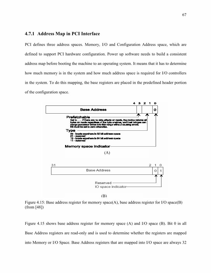
67
4.7.1 Address Map in PCI Interface PCI defines three address spaces. Memory, I/O and Configuration Address space, which are
defined to support PCI hardware configuration. Power up software needs to build a consistent
address map before booting the machine to an operating system. It means that it has to determine
how much memory is in the system and how much address space is required for I/O controllers
in the system. To do this mapping, the base registers are placed in the predefined header portion
of the configuration space.
Figure 4.15: Base address register for memor(from [48])
Figure 4.15 shows base address register for
Base Address registers are read-only and is
into Memory or I/O Space. Base Address reg
(A)
)
(B y space(A), base address register for I/O space(B)memory space (A) and I/O space (B). Bit 0 in all
used to determine whether the registers are mapped
isters that are mapped into I/O space are always 32
68
bits wide with bit 0 hard wired to a 1. Base Address registers that map into memory Space can be
32-bit or 64 bit wide with bit 0 hard wired to 0.A top-level block diagram of the PCI interface
design is shown in Figure 4.19.
Figure 4.16: PCI, DMA and User-Interface Block Diagram
4.7.2 Accessing Mailbox Registers The Mailbox Registers, explained in section 2.1, are built by a register file with size of 4KByte
(64bitx512 ), which are mapped in Memory Space. Accessing Mailbox registers is enabled by
69
Base-hit1 signal. The rows in the mailbox register are selected by lower 5-bit address of the PCI
address (Addr signal in Figure 4.19). These registers are not byte allocatable, so all 64-bits data
can be transferred to each register in one cycle. There is a copy of the Mailbox registers
implemented in Virtex-II Pro to make it easier for the Network Processor to read the Mailbox
Registers updated values, shown as the Mailbox Register File-Copy in the Figure 4.19. The
lower 5 bits of the Addr signal select mailboxes in the register. The Network processor can poll
the status to see if the Decoder-5to32 unit has updated Mailbox Register. Once the Network
processor receives the required information to initiate a transaction, it issues control commands
to DMA-Controller to start the transaction.
4.7.3 Accessing the Shared Registers The Shared registers are used by host processor to have access some part of memory in SRAM
and SDRAM or status registers in Network Processor for debugging purposes. The Shared
Registers are built by a register file with size of 4KB Byte (64bit x 512) mapped in Memory
Space Accessing to the Shared Register is enabled by Base-hit2 signal. The rows in the Shared
register are selected by 8 lower bit address of the PCI address (Addr signal). These registers are
not byte allocatable, so all 64-bits data can be transferred to each register in one cycle. Once
Basehit2 enables the Shared memory register, the address of the target memory part is set on the
ADIO bus by the host and will be stored in a 64bitx1 SharedMem_AD Register in the Virtex-II
Pro. The Memory-controller on the Virtex-II Pro part can read the address from this register.
Depending on address value, the memory controller should fetch the 64-bit data from the
DRAM, SRAM or Network Processor and write it in the SharedMem_AD.
70
5 Chapter 5
Experimental Results and Design Evaluation
The use of SDRAM in a network interface is proposed in this work to provide more memory
capacity and larger bandwidth. As discussed in chapter 2, additional memory capacity allows the
implementation of new services like network interface data caching and iSCSI in network
interface, which substantially improves server performance. This chapter evaluates the FPGA-
based NIC functionality for receiving data at Gigabit Ethernet interface and storing it in the
SDRAM with the Avnet board. To evaluate the NIC performance, throughput, latency, and bus
utilization for receiving different packet sizes are measured and analyzed. As mentioned earlier,
efficient RTL coding can enhance system performance throughput. In addition, it was pointed
that burst transfers architectures increase the bandwidth requirement in SDRAMs and improve
system performance. This chapter examines how different implementations for the bus interface
(master and slave interfaces) and SDRAM controller which were proposed in chapter 5, affect
the NIC throughput performance.
The throughput of the stored data in the SDRAM for the best implementation is
compared with that of the existing Tigon programmable NIC, which uses SRAM. This chapter
then measures the bus utilization in receive interface and analyzes the OPB efficiency for
implementation of Ethernet Transmit and DMA interfaces.
5.1 Experimental Setup To evaluate the receiver of the Gigabit Ethernet Interface, PC machines are used for sending
UDP Datagrams to the Avnet board. The machines run a simple program that sends packets with
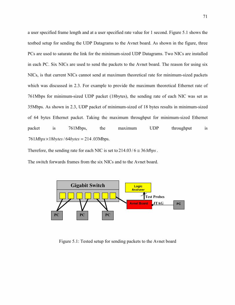
71
a user specified frame length and at a user specified rate value for 1 second. Figure 5.1 shows the
testbed setup for sending the UDP Datagrams to the Avnet board. As shown in the figure, three
PCs are used to saturate the link for the minimum-sized UDP Datagrams. Two NICs are installed
in each PC. Six NICs are used to send the packets to the Avnet board. The reason for using six
NICs, is that current NICs cannot send at maximum theoretical rate for minimum-sized packets
which was discussed in 2.3. For example to provide the maximum theoretical Ethernet rate of
761Mbps for minimum-sized UDP packet (18bytes), the sending rate of each NIC was set as
35Mbps. As shown in 2.3, UDP packet of minimum-sized of 18 bytes results in minimum-sized
of 64 bytes Ethernet packet. Taking the maximum throughput for minimum-sized Ethernet
packet is 761Mbps, the maximum UDP throughput is
21464/18761 =× bytesbytesMbps .03Mbps.
Therefore, the sending rate for each NIC is set to Mbps366/03.214 ≅ .
The switch forwards frames from the six NICs and to the Avnet board.
Figure 5.1: Tested setup for sending packets to the Avnet board
Gigabit Switch
PC PC PC
Avnet Board
Logic Analyzer
PC
Test Probes
JTAG
72
5.2 Performance Definition Performance may have different meanings for different applications, which usually includes the
throughput, packet rate, packet loss, per-packet latency, response time and efficient resource
utilization. In this work, to evaluate the performance of Gigabit Ethernet receive interface the
following parameters are used.
� Throughput- The amount of data the NIC can receive and store it in the SDRAM per unit of
time, measured in Mbps. The throughput is measured based on the total number of received
bytes for each experiment, as measured by the counters implemented in the HDL code.
� Per-packet latency- The delay that the NIC can receive data and store it in the SDRAM per
unit of time. These numbers are achieved using Tektronix Logic Analyzer timing
measurements.
� Efficient resource utilization- Resources in this part of implementation, Ethernet receive and
SDRAM interface, are memory utilization and bus utilization. The utilization numbers are
achieved using a timing model, which is based on measurements from Logic Analyzer and
counters implemented in the HDL code.
5.3 Receive Throughput As discussed in section 4, there are many factors that can influence the receive throughput In this
implementation five of these factors are more significant than the rest:
� PHY
� Gigabit Ethernet MAC
� FIFO Size
� Bus Efficiency
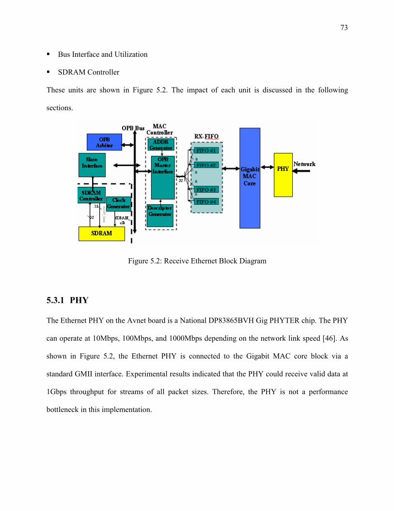
73
� Bus Interface and Utilization
� SDRAM Controller
These units are shown in Figure 5.2. The impact of each unit is discussed in the following
sections.
Figure 5.2: Receive Ethernet Block Diagram
5.3.1 PHY The Ethernet PHY on the Avnet board is a National DP83865BVH Gig PHYTER chip. The P
can operate at 10Mbps, 100Mbps, and 1000Mbps depending on the network link speed [46]
shown in Figure 5.2, the Ethernet PHY is connected to the Gigabit MAC core block v
standard GMII interface. Experimental results indicated that the PHY could receive valid da
1Gbps throughput for streams of all packet sizes. Therefore, the PHY is not a perform
bottleneck in this implementation.
HY
. As
ia a
ta at
ance
74
5.3.2 Gigabit Ethernet MAC Interface The functionality of the MAC is well defined and fixed for Ethernet protocol. For this reason, the
Xilinx Gigabit Ethernet MAC core is used for the NIC controller design. Xilinx Gigabit Ethernet
MAC provides full or half-duplex transfer at 2 Gbps or 1Gbps throughput. Experimental results
with receiving ARP packets indicated that valid ARP packets could be received and transferred
by the Gigabit MAC core at 1Gpbs throughput. This result verifies that Gigabit MAC can receive
at 1Gbps rate and it is not a performance bottleneck.
5.3.3 Impact of FIFO Size As shown in Figure 5.2 and discussed in section 4.5.1, four modules of an 8-bit wide FIFO are
used to make a 32-bit wide data for the OPB bus transfers. Comparing the ARP packets at write
and read ports of FIFO verifies the correct functionality of FIFOs. Experimental results with
continuous streams of packets indicated that changing FIFO size does not have impact on
achieved throughput in receive interface. The data is written in to the FIFO at 1Gbps (8 bit x 125
MHz) rate. If the FIFO contents are being read at a faster rate than being written, FIFO never
becomes full. Therefore, the minimum sized FIFO of 128 bytes is used for receive interface. On
the other hand, if reading the FIFO contents is slower than writing to the FIFO, FIFO will
become full. Changing the FIFO size in this case does not improve the performance. Because, for
a continuous stream of data, the FIFO eventually will become full, no matter how big the FIFO
is.
However, if other interfaces are implemented in the bus, because of arbitration delays for
the OPB bus, larger buffering is required. Ideally, it is required to implement very large FIFO
which provides enough buffering space for multiple large frames. However, the available on-
75
chip memory in FPGA is limited. Therefore, it is required to measure resource utilizations in
FIFO implementation with different sizes. As mentioned in section 4.5.1, FIFOs are
implemented using the Block Select RAMS [66] in Virtex-II Pro FPGA. Each Block Select
RAM is 18Kbit and there are 88Blocks in the XC2V20ff896 package of Virtex-II Pro. Number
of Block Select RAMs and slice counts in FIFO implementation can be found in .map reports
generation by Xilinx ISE tolls during the implementation process. Figure 5.3 shows the percent
utilization of Block Select RAMs and Slice utilization in FIFO implementation with different
depth sizes.
As shown in the Figure, the largest FIFO is implemented with depth size of 31767
words, which costs 60 Block Select RAMS or 68% of available memory. The percent utilization
of Block Select RAMs for implementing FIFO with depth sizes of 15 to 2047 does not change.
The reason is that both implementations use the same number of Block Select RAMs. For
example, implementing an 8-bit wide FIFO with depth size of 15 words requires (8 × 15) 120
bits which costs one Block Select RAM utilization. Also, implementing an 8-bit wide FIFO with
depth size of 2047 requires (8 ×2047) 16376 bits and costs one Block Select RAM. The number
of slice counts is dependent on the number of addressing bits, the number of read and write
counters and handshake signals in FIFO implementation. Increasing the FIFO size from 15 to
31767 makes the percentage of slice count utilization change from 1.5% to 3.3%.
76
0102030405060708090
100
15 31 63 127 255 511 1023 2047 4095 8191 16383 32767
FIFO Depth Size
Res
ourc
e U
tiliz
atio
n(%
) % of Total Slices
% of Total Block Select RAMs
Figure 5.3: Resource utilization for receive FIFO implementation with 8-bit wide and different depth sizes. As shown in the figure, the Block RAMs and Slices for depth sizes of 15 to 2047 is almost unchanged.
Thus, implementing the receive FIFO with depth size of 2047 provides (4× 8 × 2047) 8Kbyte
buffering space for storing u to 10 incoming frames larger than 1518 bytes. Remember that, the
receive FIFO is implemented by 4 modules of 8-bit FIFO. Compared to depth size of 15, the
buffering space is increased up to 135% with depth size of 2047, but the percentage utilization of
memory is 4.5% and remains unchanged compared to depth size of 15.
5.3.4 Bus Efficiency The Xilinx OPB is 32 bits wide and can operate at 100 MHz. Therefore, it can sustain a
maximum 3.2 Gbps throughput. Thus, for the receive interface, the OPB provides enough
bandwidth for a maximum 1Gbps throughput. However, this bandwidth is not sufficient for a
complete functional NIC.
77
5.3.5 Bus Interface and Utilization The number of cycles between two FIFO transfer should be 3.2 OPB-cycles
( Gbpsnsbit 110/32 × ) in order to achieve 1Gbps throughput. However, the number of cycles for
transferring data in OPB bus and store it in the SDRAM depends on the bus interface
implementation including arbitration process, master and slave interfaces and SDRAM
controller. The following sections show the impact of different implementations for OPB master,
OPB slave interfaces, and SDRAM controller, which were discussed in section 4.5, on the
achieved throughput.
Impact of OPB-Master Interface Design
Figure 5.4 shows the UDP receive throughputs of two different OPB master interface
implementations, which were discussed in section 4.2. The X-axis shows UDP datagram sizes
varying from 18 bytes (leading to minimum-sized 64-bytes Ethernet frames, after accounting for
20 bytes of IP headers, 8 bytes of UDP headers, 14 bytes of Ethernet headers, and 4 bytes of
Ethernet CRC) to 1472 bytes (leading to maximum-sized 1518-bytes Ethernet frames). The
Y-axis shows throughput in Mbps of UDP datagrams. The Ethernet Limit curve represents the
theoretical maximum data throughput of the UDP/IP protocol running on Ethernet for a given
datagram size. Protocol overheads, including headers and required inter-frame gaps, prevent the
full utilization of 1 Gbps for data.
As shown in figure, the throughput achieved by Xilinx OPB-master core implementation
can not exceed than 160Mbps. With custom-designed OPB-master the throughput reaches to
246Mbps. The Custom-designed OPB-master interface outperforms the Xilinx OPB-master core
interface and delivers up to 53% more throughput. However, it can not reach the Ethernet limit.
78
The low throughput bottleneck in both implementations is caused by the excessive processing
time in the OPB transfers.
Figure 5.4: UDP receive throughput achieved by different OPB-master interface implementation
Timing relationships, captured from Logic Analyzer, among signals in the receive interface are
shown in Figure 5.5 and 5.6. Timing diagram shown in these figures is for single data transfers
from FIFO to the OPB and SDRAM. Figure 5.5 shows the timing diagram for data transfers,
when Xilinx OPB-master core interface is used. As indicated in the figure, it takes 20 OPB-
cycles for each FIFO transfer to be complete. Therefore, the maximum throughput by using
Xilinx OPB-Master core cannot exceed 160Mbps ( ns1020/832 ×× ). As shown in the figure,
Xilinx OPB-master core starts OPB transfer, by asserting OPB-Select signal, 7 cycles after it gets
grant by the OPB arbiter.
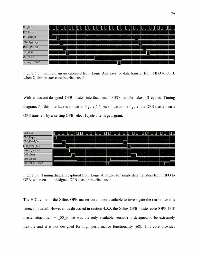
79
Figure 5.5: Timing diagram captured from Logic Analyzer for data transfer from FIFO to OPB, when Xilinx master core interface used.
With a custom-designed OPB-master interface, each FIFO transfer takes 13 cycles. Timing
diagram, for this interface is shown in Figure 5.6. As shown in the figure, the OPB-master starts
OPB transfers by asserting OPB-select 1cycle after it gets grant.
Figure 5.6: Timing diagram captured from Logic Analyzer for single data transfers from FIFO to OPB, when custom-designed OPB-master interface used.
The HDL code of the Xilinx OPB-master core is not available to investigate the reason for this
latency in detail. However, as discussed in section 4.5.5, the Xilinx OPB-master core (OPB-IPIF
master attachment v1_00_b that was the only available version) is designed to be extremely
flexible and it is not designed for high performance functionality [68]. This core provides
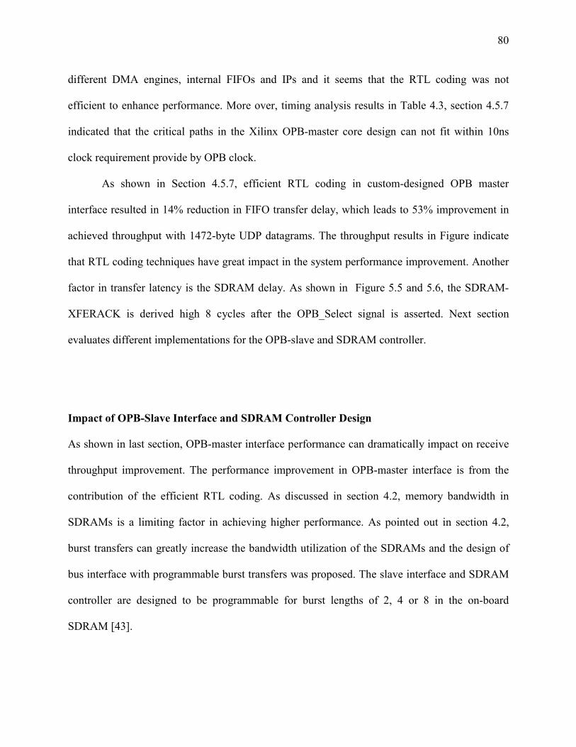
80
different DMA engines, internal FIFOs and IPs and it seems that the RTL coding was not
efficient to enhance performance. More over, timing analysis results in Table 4.3, section 4.5.7
indicated that the critical paths in the Xilinx OPB-master core design can not fit within 10ns
clock requirement provide by OPB clock.
As shown in Section 4.5.7, efficient RTL coding in custom-designed OPB master
interface resulted in 14% reduction in FIFO transfer delay, which leads to 53% improvement in
achieved throughput with 1472-byte UDP datagrams. The throughput results in Figure indicate
that RTL coding techniques have great impact in the system performance improvement. Another
factor in transfer latency is the SDRAM delay. As shown in Figure 5.5 and 5.6, the SDRAM-
XFERACK is derived high 8 cycles after the OPB_Select signal is asserted. Next section
evaluates different implementations for the OPB-slave and SDRAM controller.
Impact of OPB-Slave Interface and SDRAM Controller Design
As shown in last section, OPB-master interface performance can dramatically impact on receive
throughput improvement. The performance improvement in OPB-master interface is from the
contribution of the efficient RTL coding. As discussed in section 4.2, memory bandwidth in
SDRAMs is a limiting factor in achieving higher performance. As pointed out in section 4.2,
burst transfers can greatly increase the bandwidth utilization of the SDRAMs and the design of
bus interface with programmable burst transfers was proposed. The slave interface and SDRAM
controller are designed to be programmable for burst lengths of 2, 4 or 8 in the on-board
SDRAM [43].
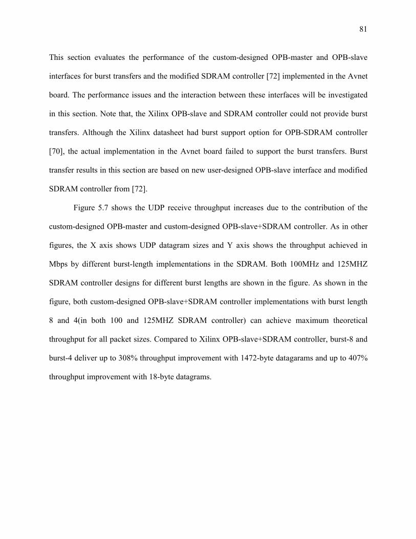
81
This section evaluates the performance of the custom-designed OPB-master and OPB-slave
interfaces for burst transfers and the modified SDRAM controller [72] implemented in the Avnet
board. The performance issues and the interaction between these interfaces will be investigated
in this section. Note that, the Xilinx OPB-slave and SDRAM controller could not provide burst
transfers. Although the Xilinx datasheet had burst support option for OPB-SDRAM controller
[70], the actual implementation in the Avnet board failed to support the burst transfers. Burst
transfer results in this section are based on new user-designed OPB-slave interface and modified
SDRAM controller from [72].
Figure 5.7 shows the UDP receive throughput increases due to the contribution of the
custom-designed OPB-master and custom-designed OPB-slave+SDRAM controller. As in other
figures, the X axis shows UDP datagram sizes and Y axis shows the throughput achieved in
Mbps by different burst-length implementations in the SDRAM. Both 100MHz and 125MHZ
SDRAM controller designs for different burst lengths are shown in the figure. As shown in the
figure, both custom-designed OPB-slave+SDRAM controller implementations with burst length
8 and 4(in both 100 and 125MHZ SDRAM controller) can achieve maximum theoretical
throughput for all packet sizes. Compared to Xilinx OPB-slave+SDRAM controller, burst-8 and
burst-4 deliver up to 308% throughput improvement with 1472-byte datagarams and up to 407%
throughput improvement with 18-byte datagrams.
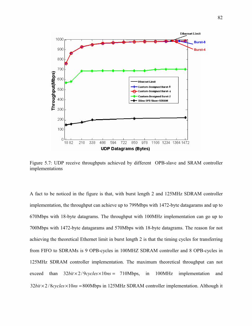
82
Figure 5.7: UDP receive throughputs achieved by different OPB-slave and SRimplementations A fact to be noticed in the figure is that, with burst length 2 and 125MHz SDR
implementation, the throughput can achieve up to 799Mbps with 1472-byte datag
670Mbps with 18-byte datagrams. The throughput with 100MHz implementatio
700Mbps with 1472-byte datagarams and 570Mbps with 18-byte datagrams. The
achieving the theoretical Ethernet limit in burst length 2 is that the timing cycles
from FIFO to SDRAMs is 9 OPB-cycles in 100MHZ SDRAM controller and 8
125MHz SDRAM controller implementation. The maximum theoretical throu
exceed than =×× nscyclesbit 109/232 710Mbps, in 100MHz implem
=×× nscyclesbit 108/232 800Mbps in 125MHz SDRAM controller implementat
Burst-8 Burst-4
AM controller
AM controller
arams and up to
n can go up to
reason for not
for transferring
OPB-cycles in
ghput can not
entation and
ion. Although it
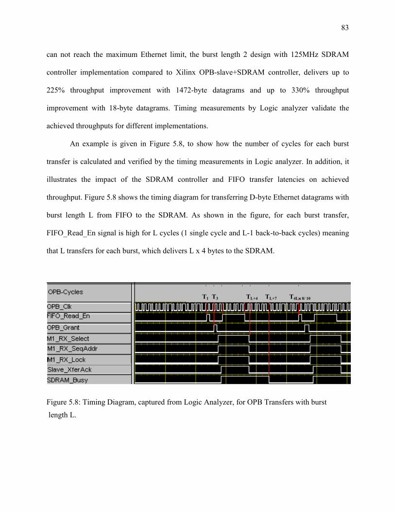
83
can not reach the maximum Ethernet limit, the burst length 2 design with 125MHz SDRAM
controller implementation compared to Xilinx OPB-slave+SDRAM controller, delivers up to
225% throughput improvement with 1472-byte datagrams and up to 330% throughput
improvement with 18-byte datagrams. Timing measurements by Logic analyzer validate the
achieved throughputs for different implementations.
An example is given in Figure 5.8, to show how the number of cycles for each burst
transfer is calculated and verified by the timing measurements in Logic analyzer. In addition, it
illustrates the impact of the SDRAM controller and FIFO transfer latencies on achieved
throughput. Figure 5.8 shows the timing diagram for transferring D-byte Ethernet datagrams with
burst length L from FIFO to the SDRAM. As shown in the figure, for each burst transfer,
FIFO_Read_En signal is high for L cycles (1 single cycle and L-1 back-to-back cycles) meaning
that L transfers for each burst, which delivers L x 4 bytes to the SDRAM.
Figure 5.8: Timing Diagram, captured from Logic Analyzer, for OPB Transfers with burst
length L.
T1 T3 TL+4 TL+7 T4L×××× 8/ 10
84
Assume that the first FIFO_Read_En is asserted in cycle T1, which is indicated in Figure 5.8. As
shown in the figure the OPB grants the bus to the receive master at cycle T3 and receive master
assumes OPB ownership and starts burst transfers by asserting the M1-RX_Select,
M1_RX_Lock, and M1_RX_SeqAddr at cycle T4. Note that the slave interface has 1 OPB-cycle
latency and the Slave-XferAck is derived by the slave interface at cycle T5 indicating that the
first data is transferred. The receive master continues to burst transfers and negates the
M1_RX_Select, M1_RX_Lock and M1_RX_SeqAddr at cycle TL+4 indicating the end of burst
transfer. To start next burst transfer two factors should be considered. First, there should be
sufficient data in the FIFO to start a burst transfer. Based on the design parameters, the required
bytes in the FIFO for starting a burst transfer is:
4bytes × L
(Note that as mentioned earlier the FIFO width is 32bits or 4 bytes.) A simple calculation
indicates that the number of bytes, which is received by FIFO during the previous burst transfer,
is:
810)L( ×+ 4 bytes (5.1)
Where L+4 is total cycles from asserting the FIFO_Read_En signal until the end of the burst.
The remaining data required to be received by FIFO for the next burst is calculated by:
810)L(L ×+− 44 bytes
The equivalent OPB-cycle is calculated by:
)L(L)8
10)L(L( 41084
10844 +−×=××+− OPB-cycles
85
Thus the number of OPB-cycles to transfer data from FIFO to OPB-slave interface is the sum of
the transfer cycles to the OPB and number of OPB-cycles waiting for FIFO to get the remaining
data which is calculated by:.
108444
1084 ×=+++−× L)L())L(L( OPB-cycles (5.2)
Therefore, receive master requires to wait for 10/84 ×L OPB-cycles and asserts the
FIFO_RD_En signal at cycle T 10/84 ×L .
Another factor, requires to be considered before starting the next burst transfer is that to
check if the SDRAM controller is done with transferring data to the SDRAM or not. As shown in
the figure, although the Slave_XferAck is negated at cycle TL+4 the SDRAM_Busy signal is
negated at cycle TL+7. This latency is due to the SDRAM controller delay, which is required to
meet the timing requirements for write process in the SDRAM. Table 5.1 shows the required
cycles to get the data to the FIFO by MAC interface and transfer it to the SDRAM by SDRAM
controller for each burst length implementation. There are three main columns in the table. The
first column is for the burst lengths, which are used in different implementations. Second
column, is the number of cycles to transfer data from MAC interface to the OPB bus, split to two
categories of OPB cycles and MAC cycles. Third column belongs to the timing cycles in
SDRAM controller during write process. Each category is again split to SDRAM-cycles and
OPB-cycles. As discussed in section 4.5.7, there are two implementations for SDRAM controller
with 100MHz clock and with 125MHz clock.
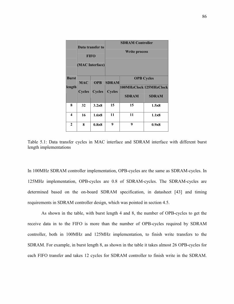
86
Data transfer to
FIFO
(MAC Interface)
SDRAM Controller
Write process
OPB Cycles
Burst
length MAC
Cycles
OPB
Cycles
SDRAM
Cycles100MHzClock
SDRAM
125MHzClock
SDRAM
8 32 3.2××××8 15 15 1.5××××8
4 16 1.6××××8 11 11 1.1××××8
2 8 0.8××××8 9 9 0.9××××8
Table 5.1: Data transfer cycles in MAC interface and SDRAM interface with different burst length implementations
In 100MHz SDRAM controller implementation, OPB-cycles are the same as SDRAM-cycles. In
125MHz implementation, OPB-cycles are 0.8 of SDRAM-cycles. The SDRAM-cycles are
determined based on the on-board SDRAM specification, in datasheet [43] and timing
requirements in SDRAM controller design, which was pointed in section 4.5.
As shown in the table, with burst length 4 and 8, the number of OPB-cycles to get the
receive data in to the FIFO is more than the number of OPB-cycles required by SDRAM
controller, both in 100MHz and 125MHz implementation, to finish write transfers to the
SDRAM. For example, in burst length 8, as shown in the table it takes almost 26 OPB-cycles for
each FIFO transfer and takes 12 cycles for SDRAM controller to finish write in the SDRAM.
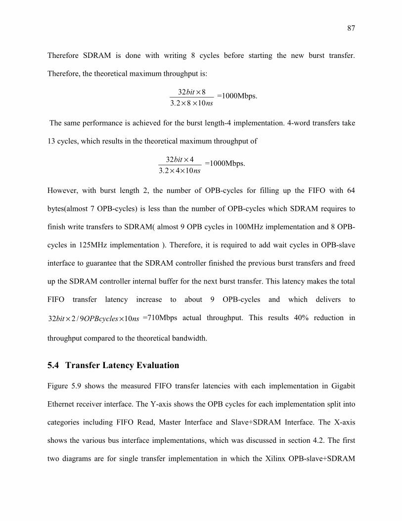
87
Therefore SDRAM is done with writing 8 cycles before starting the new burst transfer.
Therefore, the theoretical maximum throughput is:
ns.bit
10823832
××× =1000Mbps.
The same performance is achieved for the burst length-4 implementation. 4-word transfers take
13 cycles, which results in the theoretical maximum throughput of
ns.bit
10423432
××× =1000Mbps.
However, with burst length 2, the number of OPB-cycles for filling up the FIFO with 64
bytes(almost 7 OPB-cycles) is less than the number of OPB-cycles which SDRAM requires to
finish write transfers to SDRAM( almost 9 OPB cycles in 100MHz implementation and 8 OPB-
cycles in 125MHz implementation ). Therefore, it is required to add wait cycles in OPB-slave
interface to guarantee that the SDRAM controller finished the previous burst transfers and freed
up the SDRAM controller internal buffer for the next burst transfer. This latency makes the total
FIFO transfer latency increase to about 9 OPB-cycles and which delivers to
nsOPBcyclesbit 109/232 ×× =710Mbps actual throughput. This results 40% reduction in
throughput compared to the theoretical bandwidth.
5.4 Transfer Latency Evaluation Figure 5.9 shows the measured FIFO transfer latencies with each implementation in Gigabit
Ethernet receiver interface. The Y-axis shows the OPB cycles for each implementation split into
categories including FIFO Read, Master Interface and Slave+SDRAM Interface. The X-axis
shows the various bus interface implementations, which was discussed in section 4.2. The first
two diagrams are for single transfer implementation in which the Xilinx OPB-slave+SDRAM
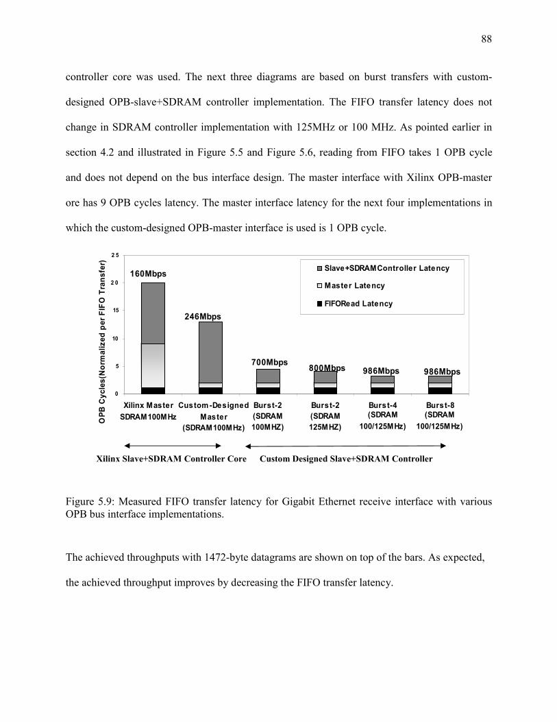
88
controller core was used. The next three diagrams are based on burst transfers with custom-
designed OPB-slave+SDRAM controller implementation. The FIFO transfer latency does not
change in SDRAM controller implementation with 125MHz or 100 MHz. As pointed earlier in
section 4.2 and illustrated in Figure 5.5 and Figure 5.6, reading from FIFO takes 1 OPB cycle
and does not depend on the bus interface design. The master interface with Xilinx OPB-master
ore has 9 OPB cycles latency. The master interface latency for the next four implementations in
which the custom-designed OPB-master interface is used is 1 OPB cycle.
Figure 5.9: Measured FIFO transfer latency for Gigabit Ethernet receive interface with various OPB bus interface implementations.
The achieved throughputs with 1472-byte datagrams are shown on top of the bars. As expected,
the achieved throughput improves by decreasing the FIFO transfer latency.
0
5
10
15
2 0
2 5
Xilinx MasterCore
Custom-Designed
Master
Burst-2(SDRAM100MHZ)
Burst-2(SDRAM125MHZ)
Burst-4 Burst-8
OPB
Cyc
les(
Nor
mal
ized
per
FIF
O T
rans
fer) Slave+SDRAMController Latency
Master Latency
FIFORead Latency
160Mbps
986Mbps700Mbps
246Mbps
800Mbps 986Mbps
(SDRAM100/125MHz)
Xilinx Master SDRAM100MHz (SDRAM
100/125MHz)
Custom -DesignedMaster
(SDRAM100MHz)
Xilinx Slave+SDRAM Controller Core Custom Designed Slave+SDRAM Controller
89
Compared to Xilinx OPB-master Core with Xilinx OPB slave+SDRAM controller
implementation, both burst-4 and 8 which are implemented by custom-designed OPB-
master+slave+SDRAM controller decrease FIFO transfer latency by 84% and increase
throughput improvement 516% with 1472-byte datagrams.
5.5 Throughput Comparison with Tigon Controller
Figure 5.10 compares the achieved throughput in Ethernet receive interfaces with Tigon
controller on 3Com NIC and FPGA-based NIC controller on Avnet board. The fact that the
FPGA-based NIC can achieve the same throughput with using SDRAM as Tigon, which is using
SRAM, is very promising. As mentioned earlier, SRAMs are faster memories than SDRAMs and
no existing NIC use SDRAM due to its memory access latency. As shown in this work the
latency disadvantage of SDRAMs can be alleviated by the efficient architecture design and RTL
programming techniques. In addition, SDRAMs provide large memory capacity and bandwidth
to support new services, like TCP offloading or network interface data caching which can
substantially improve the server performance. As mentioned earlier, current NICs can not
achieve the theoretical throughput for small packet traffic in bidirectional transfer. Current
studies indicate that the reason for this bottleneck is that current NICs do not provide enough
buffering and processing power to implement basic packet processing tasks efficiently as the
frame rate increases for small packets traffic.
90
Figure 5.10: A comparison in UDP receive throughputs achieved with Tigon controller on 3Com NIC and FPGA-based NIC controller on Avnet board.
In addition, programmable processors suffer from performance disadvantages due to the
instruction overhead bottleneck. Experimental results with 3COM NICs, which are based on
Tigon controller show that the maximum throughput achieved in a bidirectional transfer with
multiple cores implementation is about 150Mbps, 80% less than theoretical throughput [19].
Although the bidirectional transfer design is not evaluated in the FPGA-based NIC here, some
predictions on overall design performance can be made. Table 5.2 compares the hardware
configuration in Tigon-based NIC (3Com NIC) and FPGA-based NIC (Avnet board). It is clear
that two embedded PowerPC processors in the Virtex-II pro FPGA, operating at 400MHz,
provide more processing power than the two MIPS R4000 processors, operating at 88MHz, in
Tigon.
.
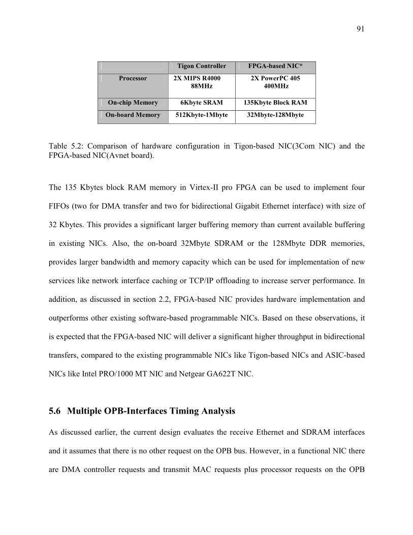
91
Tigon Controller FPGA-based NIC*
Processor 2X MIPS R4000 88MHz
2X PowerPC 405 400MHz
On-chip Memory 6Kbyte SRAM 135Kbyte Block RAM
On-board Memory 512Kbyte-1Mbyte 32Mbyte-128Mbyte
Table 5.2: Comparison of hardware configuration in Tigon-based NIC(3Com NIC) and the FPGA-based NIC(Avnet board). The 135 Kbytes block RAM memory in Virtex-II pro FPGA can be used to implement four
FIFOs (two for DMA transfer and two for bidirectional Gigabit Ethernet interface) with size of
32 Kbytes. This provides a significant larger buffering memory than current available buffering
in existing NICs. Also, the on-board 32Mbyte SDRAM or the 128Mbyte DDR memories,
provides larger bandwidth and memory capacity which can be used for implementation of new
services like network interface caching or TCP/IP offloading to increase server performance. In
addition, as discussed in section 2.2, FPGA-based NIC provides hardware implementation and
outperforms other existing software-based programmable NICs. Based on these observations, it
is expected that the FPGA-based NIC will deliver a significant higher throughput in bidirectional
transfers, compared to the existing programmable NICs like Tigon-based NICs and ASIC-based
NICs like Intel PRO/1000 MT NIC and Netgear GA622T NIC.
5.6 Multiple OPB-Interfaces Timing Analysis As discussed earlier, the current design evaluates the receive Ethernet and SDRAM interfaces
and it assumes that there is no other request on the OPB bus. However, in a functional NIC there
are DMA controller requests and transmit MAC requests plus processor requests on the OPB
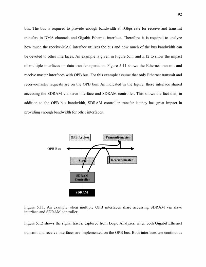
92
bus. The bus is required to provide enough bandwidth at 1Gbps rate for receive and transmit
transfers in DMA channels and Gigabit Ethernet interface. Therefore, it is required to analyze
how much the receive-MAC interface utilizes the bus and how much of the bus bandwidth can
be devoted to other interfaces. An example is given in Figure 5.11 and 5.12 to show the impact
of multiple interfaces on data transfer operation. Figure 5.11 shows the Ethernet transmit and
receive master interfaces with OPB bus. For this example assume that only Ethernet transmit and
receive-master requests are on the OPB bus. As indicated in the figure, these interface shared
accessing the SDRAM via slave interface and SDRAM controller. This shows the fact that, in
addition to the OPB bus bandwidth, SDRAM controller transfer latency has great impact in
providing enough bandwidth for other interfaces.
Figure 5.11: An example whinterface and SDRAM controll
Figure 5.12 shows the signal tr
transmit and receive interfaces
Slave Receive-master
Transmit-master OPB Arbiter
OPB Bus
SDRAM Controller
en multiple OPB interfaces share accessing SDRAM via slave er.
aces, captured from Logic Analyzer, when both Gigabit Ethernet
are implemented on the OPB bus. Both interfaces use continuous
SDRAM
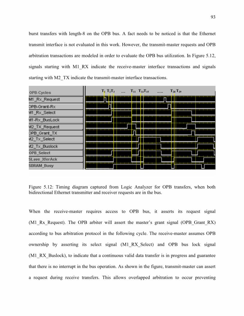
93
burst transfers with length-8 on the OPB bus. A fact needs to be noticed is that the Ethernet
transmit interface is not evaluated in this work. However, the transmit-master requests and OPB
arbitration transactions are modeled in order to evaluate the OPB bus utilization. In Figure 5.12,
signals starting with M1_RX indicate the receive-master interface transactions and signals
starting with M2_TX indicate the transmit-master interface transactions.
Figure 5.12: Timing diagram captubidirectional Ethernet transmitter and
When the receive-master require
(M1_Rx_Request). The OPB arbite
according to bus arbitration protoco
ownership by asserting its selec
(M1_RX_Buslock), to indicate that
that there is no interrupt in the bus o
a request during receive transfers.
T1 T2T3 …. T11 T14T15 .….. T28 T29
red from Logic Analyzer for OPB transfers, when both receiver requests are in the bus.
s access to OPB bus, it asserts its request signal
r will assert the master’s grant signal (OPB_Grant_RX)
l in the following cycle. The receive-master assumes OPB
t signal (M1_RX_Select) and OPB bus lock signal
a continuous valid data transfer is in progress and guarantee
peration. As shown in the figure, transmit-master can assert
This allows overlapped arbitration to occur preventing
94
arbitration penalty cycle. The OPB arbiter grants the bus to the transmit-master after the receive-
master negated the M1_RX_Select and M1_RX_Buslock signals at cycle T13. The transmit-
master interface assumes ownership of the bus by asserting M2-TX_Select at T14. However, it
can not start reading from SDRAM until it receives the acknowledge signal (Slave_XferAck)
asserted by slave at cycle T19. The slave overhead latency is due to the SDRAM controller delay
during writing to the SDRAM from last transaction. As discussed earlier and was shown in
Table 5.1, SDRAM controller with 125MHz implementation requires 12 OPB-cycles to finish
writing burst length 8 to the SDRAM. With 100MHz SDRAM controller implementation, this
latency is increased to 14 OPB-cycles. For this example, 125MHz SDRAM controller
implementation is considered. As indicated in the figure, the SDRAM_Busy signal is negated by
SDRAM controller at cycle T14 and reading from SDRAM starts at T15. As shown in Table 5.1,
reading from SDRAM is longer than writing to the SDRAM due to the RAS latency. Therefore,
the SDRAM_Busy signal is negated at cycle T28. At this cycle, receive-master starts the next
burst transfer to the SDRAM. As discussed in section 5.3.5, the receive-interface requires
transferring data with burst length 8 to the SDRAM each 26 OPB-cycles in order to achieve
theoretical Gigabit Ethernet throughput. It is clear that, with 100MHz SDRAM controller, the
bidirectional Ethernet transmit and receive can not achieve the maximum throughput. Even with
125MHZ SDRAM controller implementation, as shown in the figure it is very challenging to
have bidirectional transfers at line rate.
The above timing analysis and the results in Table 5.1, indicate that different factors are
required to be considered to achieve high throughput with multiple OPB-interfaces. In addition
to the overall bus bandwidth, the bus utilization of each interface has a great impact on
increasing the performance in network interface. Moreover, efficient SDRAM controller design
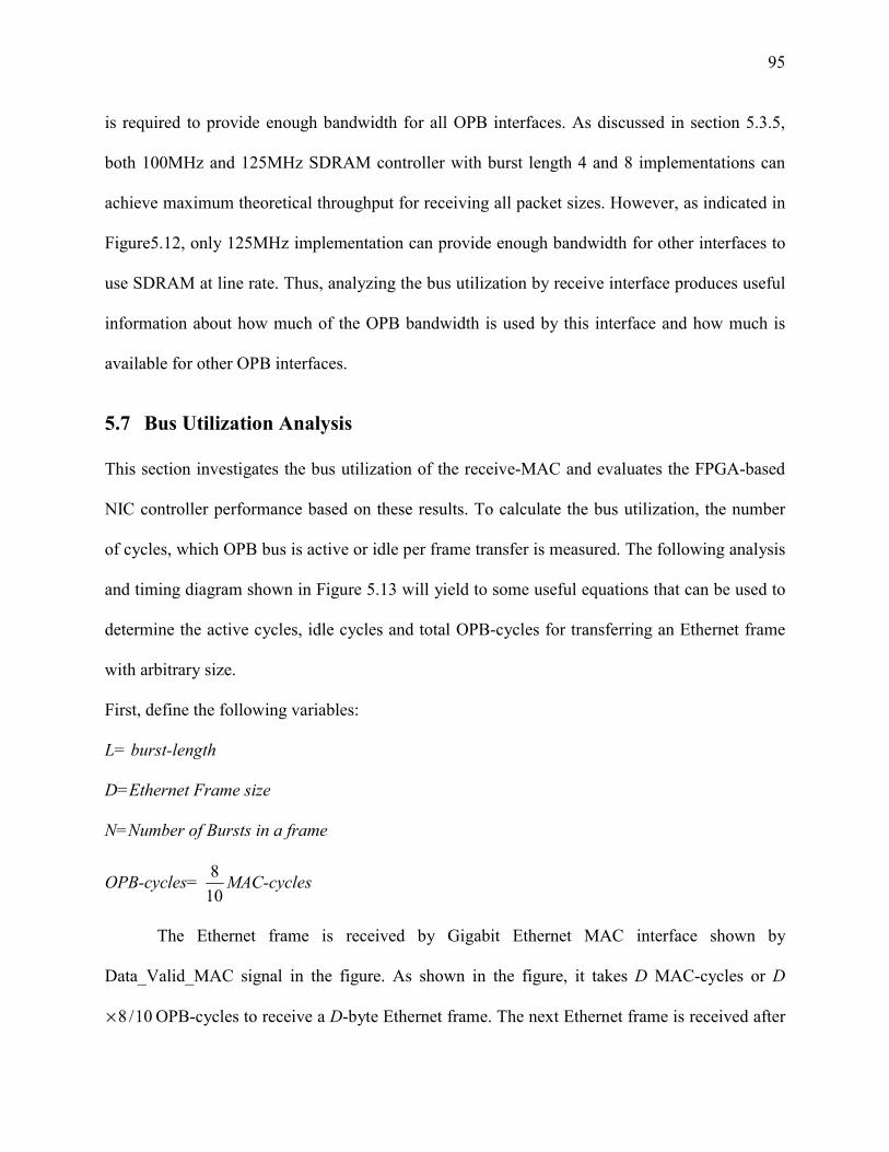
95
is required to provide enough bandwidth for all OPB interfaces. As discussed in section 5.3.5,
both 100MHz and 125MHz SDRAM controller with burst length 4 and 8 implementations can
achieve maximum theoretical throughput for receiving all packet sizes. However, as indicated in
Figure5.12, only 125MHz implementation can provide enough bandwidth for other interfaces to
use SDRAM at line rate. Thus, analyzing the bus utilization by receive interface produces useful
information about how much of the OPB bandwidth is used by this interface and how much is
available for other OPB interfaces.
5.7 Bus Utilization Analysis This section investigates the bus utilization of the receive-MAC and evaluates the FPGA-based
NIC controller performance based on these results. To calculate the bus utilization, the number
of cycles, which OPB bus is active or idle per frame transfer is measured. The following analysis
and timing diagram shown in Figure 5.13 will yield to some useful equations that can be used to
determine the active cycles, idle cycles and total OPB-cycles for transferring an Ethernet frame
with arbitrary size.
First, define the following variables:
L= burst-length
D=Ethernet Frame size
N=Number of Bursts in a frame
OPB-cycles= 108 MAC-cycles
The Ethernet frame is received by Gigabit Ethernet MAC interface shown by
Data_Valid_MAC signal in the figure. As shown in the figure, it takes D MAC-cycles or D
10/8× OPB-cycles to receive a D-byte Ethernet frame. The next Ethernet frame is received after
96
20 MAC-cycle frame gap. As pointed earlier, there is a gap between each Ethernet frame, which
should be considered in calculating the idle cycles during frame transfer. This gap is determined
by the number of MAC-cycles for Preamble (8 bytes) plus interframe gap (12 bytes) which
results in 20MAC-cycles. Frame transfer over the OPB bus is shown by the M1_RX_Select,
which denotes the OPB select signal derived by the receive-master interface.
Figure 5.13: diagram for frame transfer over MAC interface and OPB interface
To determine the active cycles for each frame transfer, it is enough to know total number of
cycles that OPB select signal is asserted by the receive-master, meaning that M1_RX_Select
signal is high. Idle cycles, the cycles, which M1_RX_Select is not asserted, are determined by
adding three factors. These factors are the number of OPB-cycles waiting for FIFO to start the
first burst transfer, the number of OPB cycles after finishing each burst and waiting for the next
burst, finally the number of OPB-cycles waiting between each Ethernet frame. The number of
idle cycles for starting the first burst transfer (4L×8/10+4 OPB-cycles) and the number of cycles
between each burst (4L×8/10 OPB-cycles) are calculated in section 5.3.5, equation 5.2, and their
values are shown in Figure 5.13.
A fact needs to be noticed is that, this timing analysis is applied for burst length 4 and 8
implementation, which could achieve the theoretical throughput. Transferring each frame in the

97
OPB bus with burst length 4 and 8 always ends before the next frame arrives at Gigabit Ethernet
interface. Knowing this fact, the cycles between each frame transfer over the OPB bus are
determined by subtracting the number of frame transfer cycles at MAC interface and frame
transfer cycles at OPB interface. This can be determined by the following simple equations:
The number of bursts is determined by:
4×=
LDN
The number of active cycles is determined by:
N)L( ×+1 OPB-cycles
As shown in the figure, total frame transfer cycles in the MAC interface is calculated by :
16108
10820
108 +×=×+× DD OPB-cycles
The number of OPB cycles waiting to start the first burst in each frame transfer is calculated by:
41084 +×L OPB-cycles
Therefore, total cycles are calculated by:
510841
108414
1084 ++×=++××−++× LNLL)L()N(L OPB-cycles
Substituting N withL
D4
, the total transfer cycles are:
5108 ++× LD OPB-cycles (5.3)
The idle cycles in between each frame transfer in OPB is calculated by subtracting total frame
transfer cycles in MAC interface and frame transfer cycles in OPB interface, which is:
)LD()D( 510816
108 ++×−+× =11-L (5.4)

98
As indicated in the equation, the number of idle cycles between each frame transfer in OPB bus
is independent of the frame size but varies with burst length. In bus utilization measurement, it is
required to determine that how much of the active cycles are actual data transfers cycles. Data
cycles are calculated based on the total data transfers for each frame. Here, overhead cycles are
due to 1 cycle OPB-slave interface latency in each burst transfer. Therefore, overhead cycles in
each frame transfer can be easily determined by the number of bursts, which is 4/ ×LD .Thus
overhead reduction in burst length L1 to burst length L2 is determined by:
12
LL (5.5)
As indicated in the table, compared to burst length 4, burst length 8 implementation reduces the
overhead cycles by 50% for all packet sizes which can easily determined by equation(5.5).
Figure 5.14 shows the comparison of OPB bus utilization measurements for burst length
8 and 4 implementations during receiving Gigabit Ethernet frames. The X axis shows UDP
datagrams with different packet sizes. The Y axis shows the OPB bus utilization split to data
cycles and overhead cycles categories.
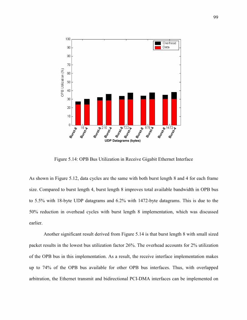
99
Figure 5.14: OPB Bus Utilization in Receive Gigabit Ethernet Interface
As shown in Figure 5.12, data cycles are the same with both burst length 8 and 4 for each frame
size. Compared to burst length 4, burst length 8 improves total available bandwidth in OPB bus
to 5.5% with 18-byte UDP datagrams and 6.2% with 1472-byte datagrams. This is due to the
50% reduction in overhead cycles with burst length 8 implementation, which was discussed
earlier.
Another significant result derived from Figure 5.14 is that burst length 8 with small sized
packet results in the lowest bus utilization factor 26%. The overhead accounts for 2% utilization
of the OPB bus in this implementation. As a result, the receive interface implementation makes
up to 74% of the OPB bus available for other OPB bus interfaces. Thus, with overlapped
arbitration, the Ethernet transmit and bidirectional PCI-DMA interfaces can be implemented on
UDP Datagrams (bytes)
100
the OPB to make a complete functional NIC transfer. Of course, any additional interface should
be implemented based on the efficient architectures and RTL programming techniques, which
were discussed on section. For other frame sizes, with half-duplex Gigabit Ethernet transfer,
bidirectional PCI-DMA transfers can be implemented on the OPB bus. The reason is that Xilinx
OPB bandwidth is 3.2 Gbps (32 x 100MHz), if both transfer and receiver are implemented,
taking 2 Gbps bandwidth of OPB, there will be 1.2 Gbps left for implementing the PCI transfers
which is not enough for bidirectional Gigabit bandwidth transfers.
101
5.8 Summary SDRAM memories provide larger memory capacity and higher bandwidth than SRAMs.
However, due to their access time latency, it is difficult to achieve their maximum theoretical
bandwidth. This chapter evaluates the FPGA-based NIC functionality in the Ethernet receiver
interface. It investigates how improving the processing latency of each interface can improve the
overall achieved throughput, transfer latency and bus utilization.
Experimental results show that increasing FIFO size up to 8Kbytes does not affect on
on-chip memory utilization. Therefore, the receive FIFO can provide enough buffering space for
up to 10 incoming large frame with size of 1518 bytes which can improve the performance in
receiving small sized packet.
Adding pipelined stages and improving the RTL coding in OPB interface
implementations lead to the reduction of latency in bus interface operations. Reduction in latency
in OPB-master interface lead to 32% reduction in total data transfer latency and 72.5%
improvement throughput for OPB single transfers.
The results presented in this section imply that, using burst transfers can alleviate the
SDRAM access time latency and results in throughput improvement and bus utilization
reduction. Burst length 4 and 8 implementations can reduce the transfer latency to 84% and
deliver up to 516.25 % more throughput, compared to SDRAM single transfer implementation.
In addition, the experimental results with burst length 4 and 8 indicate that the FPGA-based NIC
can receive all packet sizes and store them at SDRAM at Gigabit Ethernet line rate.
Using efficient architectures in SDRAM controller, such as implementation with faster
clock rate than OPB clock by using the on-chip DCMs, allows faster access time in memory
interface. Compared to 100MHz SDRAM controller, the 125MHz implementation reduces the
102
SDRAM operation cycles to 20%. This results in reduction of total transfer latency and increases
the available bandwidth for other OPB bus interfaces.
The bus utilization measurements reveal that the receive interface with minimum sized
frame and burst length 8 implementation consumes only 26% of the OPB bus. As a result, the
receive interface implementation makes up to 74% of the OPB bus available for other OPB bus
interfaces. Thus, with overlapped arbitration, the Ethernet transmit and bidirectional PCI-DMA
interfaces can be implemented on the OPB to make a complete functional NIC transfer. Of
course, any additional interface should be implemented based on the efficient architectures and
RTL programming techniques, which were discussed in section 4.5.7.
Thus, the FPGA-based Gigabit Ethernet NIC is a viable platform to achieve throughput
competitive with ASIC-based NICs for real time network services. Such a research platform
provides a valuable tool for systems researchers in networking to explore efficient system
architectures and services to improve server performance.
103
6 Chapter 6 Conclusions and Future work
6.1 Conclusions The continuing advances in the performance of network servers make it essential for network
interface cards (NICs) to provide services that are more sophisticated rather than simple data
transfering. Modern network interfaces provide fixed functionality and are optimized for sending
and receiving large packets. Previous research has shown that both increased functionality in the
network interface and increased bandwidth on small packets can significantly improve the
performance of today's network servers. One of the key challenges for networking systems
researchers is to find effective ways to investigate novel architectures for these new services and
evaluate their performance characteristics in a real network interface platform. The development
of such services requires flexible and open systems that can easily be extended to enable new
features.
This thesis presents the design and evaluation of a flexible and configurable Gigabit
Ethernet/PCI network interface card using FPGAs. This system is designed as an open research
platform, with a range of configuration options and possibilities for extension in both software
and hardware dimensions. This FPGA-based NIC features two types of volatile memory. A
pipelined ZBT (Zero Bus Turnaround) SRAM device is used as a low latency memory to allow
the network processor to access the code. The other memory is a 128 Mbytes SDRAM SO-
DIMM, a large capacity and high bandwidth memory, which is used for data storage and adding
future services like network interface data caching [20]. This thesis first presents the design of
the hardware platform for the FPGA-based Gigabit Ethernet/ PCI NIC. Then the thesis shows a
104
high-performance architecture for a functional Gigabit Ethernet/PCI network interface controller
in the FPGA.
The performance of Gigabit Ethernet receive interface is evaluated in the Avnet board.
The experimental results indicate that adding pipelined stages and improving the RTL coding in
the design, lead to the reduction of latency in bus interface operations, which results to 32%
reduction in total data transfer latency between receive FIFO and SDRAM and 72.5%
improvement in achieved throughput with single transfers in OPB Bus interface.
The results presented in this thesis imply that, using burst transfers can alleviate the
SDRAM access latency and results in throughput improvement and bus utilization reduction.
Compared to SDRAM single transfer implementation, implementation with burst length 4 and 8
can reduce the FIFO transfer latency to 84% and deliver up to 516.25 % more throughput in
received maximum-sized 1518-byte Ethernet packet. In addition, the experimental results with
burst length 4 and 8 indicate that the FPGA-based NIC can receive all packet sizes and store
them in the SDRAM at Gigabit Ethernet line rate. This is a promising result since no existing
network interface card use SDRAM due to SDRAM latency. Increasing the working frequency
of SDRAM controller to 125MHz, 25% faster than the processor bus clock, allows faster access
time in memory interface. Compared to 100MHz SDRAM controller, the 125MHz
implementation reduces the SDRAM operation cycles to 20%. This results in reduction of total
transfer latency and increases the available bandwidth for other OPB bus interfaces.
The bus utilization measurements indicate that the receive interface with minimum sized
Ethernet frame of 64-byte and burst length 8 implementation consumes only 26% of the OPB
bus. As a result, the receive interface implementation makes up to 74% of the OPB bus available
for other OPB bus interfaces. Thus, with overlapped arbitration, the Ethernet transmit and
105
bidirectional PCI-DMA interfaces can be implemented on the OPB to make a complete
functional NIC transfer. Of course, any additional interface should be implemented based on the
efficient architectures and RTL programming techniques, which were discussed in section 4.5.7.
Thus, this thesis shows that the FPGA-based Gigabit Ethernet NIC is a viable platform to
achieve throughput competitive with ASIC-based NICs for real time network services. Such a
research platform provides a valuable tool for systems researchers in networking to explore
efficient system architectures and services to improve server performance.
6.2 Future Work The preliminary experimental results on the receiver of the Gigabit Ethernet proved that FPGA-
based NIC with SDRAM is capable of being a functional NIC. Moreover, these results
confirmed that the FPGA-based NIC have the potentiality to achieve the wire speed of Gigabit
Ethernet. We would like to extend this work to evaluate the Gigabit Ethernet transmitter and PCI
interface. However, as mentioned earlier, the OPB bus, the Xilinx version, is not able to provide
enough bandwidth for each interface in Gigabit Ethernet network interface card. For future
directions, the PLB bus, which has 64-bit data width and provides 6.4Gbps rate is suggested.
Moreover, PLB supports split bus transactions, which can enhance the performance.
Implementing the synchronizing FIFOs, using on-chip Block Select RAMs can be extended for
Ethernet transmitter and PCI interface. Each FIFO can be implemented with 32-Kbyte size
RAM. The on-board SRAM must be used to store the source code for processor. Using SRAM
for storing the code results in increased available BlockSelect RAMs for FIFO implementation.
The experimental results implied that efficiently designed memory controller, which can
schedule memory accesses in DRAM can alleviate the access latency bottleneck in SDRAM.

106
Also, using the on-board DDR-Dimm memory which has 64-byte data width and operates at
133MHz can significantly increase the memory bandwidth.
107
References [1] Abhay Maheshwari, Soon-Shin Chee, “Board Routability Guidelines with Xilinx Fine-Pitch BGA Packages”, Xilinx Application Notes, XAPP157 (v1.2), November 2002. [2] Amp Inc, “MICTOR SB Connector”, Product information, Engineering Test Report:
CTLB042234-005, June 2002. [3] Austin Lesea and Mark Alexander, “Powering Xilinx FPGAs”, Xilinx Application Notes,
XAPP158 (v1.5), August 2002. [4] Alteon Networks, “Tigon/PCI Ethernet Controller”, Revision 1.04, August 1997. [5] Alteon WebSystems, “Gigabit Ethernet/PCI Network Interface Card: Host/NIC Software Interface Definition”, Revision 12.4.13, July 1999. [6] Avnet Inc. “Xilinx Virtex-II Pro Development Kit”, Released Literature # ADS- 003704, Rev.1.0, April 2003. [7] Bruce Oakley, Bruce Brown, “Highly Configurable Network Interface Solutions on a
Standard Platform”, AMIRIX Systems Inc., v.1, 2002. [8] Boden, Nan, Danny Cohen, Robert E. Felderman, Alan E. Kulawik, Charles L. Seitz,
Jakov N. Seizovic, and Wen-King Su “Myrinet, a Gigabit per Second Local Area Network”, IEEE-Micro, Vol.15, No.1, pp.29-36, February 1995.
[9] Carol Fields, “Design Reuse Strategy for FPGAs”, Xilinx Design Solutions Group,
XCell 37, 2003. [10] Cern Lab, “Report on Gigabit-Ethernet To HS Link Adapter Port”, Application, Refinement and Consolidation of HIC Exploiting Standards, 1998. [11] Charles E. Spurgeon. “Ethernet The Definitive Guide” O’Reilly & Associates, Inc.2000. [12] Cypress Semiconductor Inc. “Pipelined SRAM with NoBL Architecture” Documen#38-05161, Rev.D, November 2002. [13] Cypress Semiconductor Corporation. “512K x 32 Static RAM CY7C1062AV33” Document #: 38-05137. Rev.B, October 2002.
108
[14] F. Petrini, S. Coll, E. Frachtenberg, and A. Hoisie. “Hardware- and Software-Based
Collective Communication on the Quadrics Network”. In IEEE International Symposium on Network Computing and Applications 2001, (NCA 2001), Boston, MA, February 2002.
[15] Fabrizio Petrini, Adolfy Hoisie, Wu chun Feng, and Richard Graham. “Performance
Evaluation of the Quadrics Interconnection Network”. In Workshop on Communication Architecture for Clusters (CAC '01), San Francisco, CA, April 2001.
[16] Field Programmable Port Extender Homepage, Available from: ”http://www.arl.wustl.edu/projects/fpx”, Aug.2000. [17] H. Duan, J. W. Lockwood, and S. M. Kang, “FPGA prototype queuing module for high
performance ATM switching,” in Proceedings of the Seventh Annual IEEE International ASIC Conference, (Rochester,NY), p.429, September 1994.
[18] H. Duan, J. W. Lockwood, S. M. Kang, and J. Will, ”High-performance OC-12/OC-48
queue design prototype for input bered ATM switches”, INFOCOM97, p.20, April 1997. [19] H. Kim, “Improving Networking Server Performance with Programmable Network
Interfaces”, RICE University, Master’s thesis, April, 2003. [20] H. Kim, V. S. Pai, and S. Rixner. “Improving Web Server Throughput with Network
Interface Data Caching”. In Proceedings of the Tenth International Conference on Architectural Support for Programming Languages and Operating Systems, pp 239–250, October 2002.
[21] H. Kim, V. Pai, S. Rixner. “Exploiting Task-Level Concurrency in a Programmable
Network Interface”. In Proceedings of ACM SIGPLAN Symposium on Principles and Practices of Parallel Programming (PPoPP), June 2003.
[22] Heidi Ziegler, Byoungro So, Mary Hall, Pedro C. Diniz, “Coarse-Grain Pipelining on
Multiple FPGA Architectures”, University of Southern California / Information Sciences Institute, 2001.
[23] Hennessy & Patterson, “Computer Architecture: a quantitative approach”, Morgan
Kaufmann publishers INC, 1996. [24] Howard W. Johnson, Martin Graham. “High-Speed Digital Design, A Handbook of
BlackMagic”. Prentice Hall PTR, 1993. [25] I. Choi, “An Asynchronous Transfer Mode (ATM) Network Interface Card Using a
Multi-PLD Implementation”, In Proceedings of IEEE International ASIC Conference, 1994.
109
[26] Ian Pratt and Keir Fraser. “Arsenic: A User-Accessible Gigabit Ethernet Interface”, In
Proceedings of IEEE INFOCOM ’01, pp 67–76, 2001. [27] IBM Corporation, “On-Chip Peripheral Bus Architecture Specifications”, Document no:
SA-14- 2528-02, (V 2.1), pp. 1-50, 2001.
[28] Intel Inc, “LXT1000 Gigabit Ethernet Transceiver”, Intel DataSheets, Order no: 249276-002, July 2001.
[29] Intel Inc, “Small Packet Traffic Performance Optimization for 8255x and 8254x Ethernet Controllers”, Application Note (AP-453), 2003. [30] Jepp Jessen, Amit Dhir. “Programmable Network Processor Platform”, Xilinx Case
Study, 2003. [31] J. Satran, K. Meth, C. Sapuntzakis, M. Chadalapaka, and E. Zeidner. iSCSI. IETF
“Internet draft draft-ietf-ips-iscsi-14.txt”, work in progress, July 2002. [32] J.W. Lockwood, H. Duan, J. J.Morikuni, S.M. Kang, S. Akkineni, and R. H. Campbell,
“Scalable optoelectronic ATM networks: The iPOINT fully functional testbed,” IEEE Journal of Lightwave Technology, pp. 1093–1103, June 1995.
[33] J. W. Lockwood, N. Naufel, J. S. Turner, and D. E. Taylor, “Reprogrammable
network packet processing on the field programmable port extender (fpx),” in ACM International Symposium on Field Programmable Gate Arrays (FPGA’2001), (Monterey,CA), pp. 87–93, February. 2001.
[34] J. W. Lockwood, J. S. Turner, and D. E. Taylor, “Field programmable port extender
(FPX) for distributed routing and queuing," in FPGA'2000, (Monterey, CA), February.2000.
[35] J. W. Dawson, D. Francis, S. Haas, J. Schlereth, “High Level Design of Gigabit Ethernet S-LINK LSC”, Atlas DAQ, V.1.3, October. 2001. [36] K.C. Chang. “Digital Design and Modeling with VHDL and Synthesis”. IEEE Computer Society Press, 1997. [37] M. Bossardt, J. W. Lockwood, S. M. Kang, and S.-Y. Park, “Available bit rate
architecture and simulation for an input queued ATM switch," in GLOBECOM'98, November. 1998. [38] Mark Alexander, “Power Distribution System (PDS) Design: Using Bypass/ Decoupling
Capacitors”, Xilinx Application Notes, XAPP623 (v1.0), August 2002
110
[39] M. Weinhardt and W. Luk., “Pipelined vectorization for reconfigurable systems”, in Proc.
IEEE Symposium of FPGAs for Custom Computing Machines, 1999. [40] Micron Technology Inc., “SMALL-OUTLINE SDRAM MODULE -128MB
MT8LSDT3264H “, Micron Datasheets, SD8C8_16_32X64HG_B.fm, Rev. B- 9/021, 2002.
[41] Micron Technology Inc., “8Mb ZBT® SRAM”, Micron Datasheets, MT55L512L18P_C,
Rev. 2, 2002. [42] Micron Technology Inc., “Bypass Capacitor Selection for Highspeed Designs Technical
Note”, TN-00-06 Rev. 9, 1999. [43] Micron Technology Inc., “128Mb: x16, x32, MOBILE SDRAM”, Micron Datasheets,
Rev. H, 2001 [44] Model Sim Inc., “Modelsim Xilinx User’s Manual.”, Available from:
http://www.model.com. [45] Myricom Inc., “Myrinet Software and Customer Support”, Available from:
http://www.myri.com/scs/GM/doc, 2003. [46] National Semiconductor, “DP83865BVH Gig PHYTER® V 10/100/1000 Ethernet
Physical Layer”, September 2002. [47] Nick Tredennick, Brion Shimamoto, “Go Reconfigure”, Special report in IEEE Spectrum,
pp. 36-41, December 2003. [48] PCI Special Interest Group. “PCI Local Bus Specification”, Rev.1.0, December 1995. [49] PCI Special Interest Group.” PCI-X Addendum to the PCI Local Bus Specification”,
Rev.1.0, December 1999. [50] Peter Alfke, Bernie New “Implementing State Machines in LCA Devices”, Xilinx
Application Notes, XAPP 027, 2001. [51] Quadrics Supercomputers World Ltd., Quadrics Documentation Collection.
http://www.quadrics.com/onlinedocs/Linux/html/index.html. [52] Raoul Bhoedjang, Tim rul, Henir E.Bal, “Design Issues for User-Level Network Interface Protocols on Myrinet”, IEEE Computer, November 1998. [53] Rhett Whatcott, “Timing Closure”, TechXclusives Notes, January 2002.
111
[54] S. Hauck, “The roles of FPGAs in reprogrammable systems," Proceedings of the IEEE, vol. 86, p.615, April. 1998. [55] S. Kelem, “Virtex configuration architecture advanced user's guide." Xilinx XAPP151, September 1999. [56] Samsung Electronics Inc, “M464S1724DTS PC133/PC100 SODIMM”. Rev. 0.1.
September 2001. [57] Scott Rixner, William J. Dally, Ujval J. Kapasi, Peter Mattson, and John D. Owens.
“Memory Access Scheduling”, In Proceedings of the 27’th International Symposium on Computer Architecture, June 2000.
[58] Stephen H.Hall, Garriet W.Hall, James A. McCall. “High–Speed Digital System Design, A Handbook of Theory and Design Practices”, John Wiley and Sons, Inc. (V.3), 2000. [59] Stephanie Tapp, “Configuration Quick Start Guidelines”, Xilinx Application Notes,
XAPP501 (v1.3), June 2002. [60] The S-LINK Interface Specification, available from: http://www.cern.ch/HSI/s-
link/spec/spec CERN, 1997. [61] W. Yu, D. Buntinas, and D. K. Panda, “High Performance and Reliable NIC-Based
Multicast over Myrinet/GM-2”, In Proceedings of the International Conference on Parallel Processing (ICPP’03), October 2003.
[62] W.Westfeldt, “Internet reconfigurable logic for creating web-enabled devices.” Xilinx Xcell, Q1 1999. [63] Xilinx Inc, “MicroBlaze Reference Guide. EDK (v3.2)”, Available from:
http://www.xilinx.com/ise/embedded/edk_docs.htm, April 2003. [64] Xilinx Inc, “Spartan-II FPGA complete data sheet”, Advance Product Specification,
DS001 (v2.3), November 2001. [65] Xilinx Inc, “Virtex-II 1.5v FPGA complete data sheet”, Advance Product Specification,
DS031 (v1.7), 2001 [66] Xilinx Inc, “Virtex-II Pro™ Platform FPGA User Guide”, Xilinx User Guide, UG012
(v2.3), March 2003. [67] Xilinx Inc, “OPB IPIF Architecture”, Product Specification, DS414 (v1.3), January 2003.
112
[68] Xilinx Inc, “OPB IPIF Master Attachment”, Product Specification, DS409 (v1.2),
January 2003. [69] Xilinx Inc, “OPB IPIF Slave Attachment”, Product Specification, DS408 (v1.2), January
2003. [70] Xilinx Inc, “OPB Synchronous DRAM(SDRAM) Controller”, Xilinx Product
Specification, DS426 (1.11), February 2003. [71] Xilinx Inc, “Processor IP User Guide” Xilinx Advanced Product Specification, (v1.5), pp.1-27, June 2003. [72] Xilinx Inc, “Synthesizable High-Performance SDRAM Controllers”, Xilinx Application
Notes, XAPP134 (v3.2), November 2002. [73] Xilinx Inc, “Design Reuse Methodology for ASIC and FPGA Designers”, Advance Product Specification, XAPP249, February 2001. [74] Xilinx Inc, “Synthesizable High Performance SDRAM Controller”, XAPP134, June 2000. [75] Xilinx Inc,“Timing Constraints for Virtex-II Pro Designs” XAPP640 (v1.1) January 2003. [76] Xilinx Inc, “System ACE MPM Solution”, Preliminary Product Specification, DS087
(v2.0), February 2003. [77] Xilinx Inc, “Virtex FPGA Series Configuration and Readback” Application Notes,
XAPP138 (v2.7), July 2002. [78] Xilinx Inc, “Virtex Configuration Guide”, Xilinx User Guide, UG001 (v1.0), September
2000. [79] Xilinx Inc, “1-Gigabit Ethernet MAC Core with PCS/PMA Sublayers (1000BASE-X) or
GMII v2.1”, Xilinx Product Specification, DS200, November 2002. [80] Xilinx Inc, “ FPGA Xpower tutorial”. Available from:
http://toolbox.xilinx.com/docsan/xilinx5/help/xpower/xpower.htm. [81] Xilinx Inc, “ FPGA Timing Analyzer tutorial”. Available from:
http://toolbox.xilinx.com/docsan/xilinx5/help/timingan/timingan.htm. [82] Xilinx Inc,”ISE 5.2i help”, available from:
“http://www.xilinx.com/support/sw_manuals/xilinx5/index.htm”, DS- 0402127, 2003. [83] Xilinx Inc,”LogiCORE™PCI Design Guide”, Xilinx Intellectual Property Solutions (v
3.0), September 2002.
113
[84] Xilinx Inc,”LogiCORE™ PCI Implementation Guide”, Xilinx Intellectual Property
Solutions (v3.0), October 2002. [85] Xilinx Inc,”PowerPC Processor Reference Guide”, Embedded Development Kit EDK
(v3.2), pp.25-32, February, 2003 [86] Xilinx Inc, “PowerPC Embedded Processor Solution” available from: http://www.xilinx.com/xlnx/xil_prodcat_product.jsp?title=v2p_powerpc [87] Jason Hatashita, James Harris, Hugh Smith and Phillip L. Nico, “An Evaluation
Architecture for a Network Coprocessor”, In proceedings of the 2002 IASTED International Conference on Parallel and Distributed Computing and Systems (PDCS), November, 2002.