Embed Size (px)
Citation preview
RF/IF Vector MultiplierData Sheet ADL5390
Rev. A Document Feedback Information furnished by Analog Devices is believed to be accurate and reliable. However, no responsibility is assumed by Analog Devices for its use, nor for any infringements of patents or other rights of third parties that may result from its use. Specifications subject to change without notice. No license is granted by implication or otherwise under any patent or patent rights of Analog Devices. Trademarks and registered trademarks are the property of their respective owners.
One Technology Way, P.O. Box 9106, Norwood, MA 02062-9106, U.S.A.Tel: 781.329.4700 ©2004–2017 Analog Devices, Inc. All rights reserved. Technical Support www.analog.com
FEATURES Matched pair of multiplying VGAs Broad frequency range 20 MHz to 2.4 GHz Continuous magnitude control from +5 dB to −30 dB Output third-order intercept 24 dBm Output 1 dB compression point 11 dBm Output noise floor −148 dBm/Hz Adjustable modulation bandwidth up to 230 MHz Fast output power disable Single-supply voltage 4.75 V to 5.25 V
APPLICATIONS PA linearization and predistortion Amplitude and phase modulation Variable matched attenuator and/or phase shifter Cellular base stations Radio links Fixed wireless access Broadband/CATV RF/IF analog multiplexer
FUNCTIONAL BLOCK DIAGRAM VPS2OBBMQBBP
INPI
INMI
DSOPIBBMIBBP
RFOP
RFOM
0495
4-00
1
VPRF
CMOP
INMQ
INPQ
CMRF
Figure 1.
GENERAL DESCRIPTION The ADL5390 vector multiplier consists of a matched pair of broadband variable gain amplifiers whose outputs are summed. The separate gain controls for each amplifier are linear-in-magnitude. If the two input RF signals are in quadrature, the vector multiplier can be configured as a vector modulator or as a variable attenuator/phase shifter by using the gain control pins as Cartesian variables. In this case, the output amplitude can be controlled from a maximum of +5 dB to less than –30 dB, and the phase can be shifted continuously over the entire 360° range. Since the signal paths are linear, the original modulation on the inputs is preserved. If the two signals are independent, then the vector multiplier can function as a 2:1 multiplexer or can provide fading from one channel to another.
The ADL5390 operates over a wide frequency range of 20 MHz to 2400 MHz. For a maximum gain setting on one channel at 380 MHz, the ADL5390 delivers an OP1dB of 11 dBm, an OIP3 of 24 dBm, and an output noise floor of −148 dBm/Hz. The gain and phase matching between the two VGAs is better than 0.5 dB and 1°, respectively, over most of the operating range.
The gain control inputs are dc-coupled with a ±500 mV differential full-scale range centered about a 500 mV common mode. The maximum modulation bandwidth is 230 MHz, which can be reduced by adding external capacitors to limit the noise bandwidth on the control lines.
Both the RF inputs and outputs can be used differentially or single-ended and must be ac-coupled. The impedance of each VGA RF input is 250 Ω to ground, and the differential output impedance is nominally 50 Ω over the operating frequency range. The DSOP pin allows the output stage to be disabled quickly to protect subsequent stages from overdrive. The ADL5390 operates off supply voltages from 4.75 V to 5.25 V while consuming 135 mA.
The ADL5390 is fabricated on Analog Devices’ proprietary, high performance 25 GHz SOI complementary bipolar IC process. It is available in a 24-lead, Pb-free CSP package and operates over a −40°C to +85°C temperature range. Evaluation boards are available.
ADL5390 Data Sheet
Rev. A | Page 2 of 23
TABLE OF CONTENTS Features .............................................................................................. 1 Applications ....................................................................................... 1 Functional Block Diagram .............................................................. 1 General Description ......................................................................... 1 Specifications ..................................................................................... 3 Absolute Maximum Ratings ............................................................ 5
ESD Caution .................................................................................. 5 Pin Configuration and Function Descriptions ............................. 6 Typical Performance Characteristics ............................................. 7 General Structure ........................................................................... 11
Theory of Operation .................................................................. 11 Noise and Distortion .................................................................. 11
Applications Information .............................................................. 12
Using the ADL5390 .................................................................... 12 RF Input and Matching ............................................................. 12 RF Output and Matching .......................................................... 13 Driving the I-Q Baseband Gain Controls ............................... 13 Interfacing to High Speed DACs .............................................. 14 Generalized Modulator ............................................................. 15 Vector Modulator ....................................................................... 15 Vector Modulator Example—CDMA2000 ............................. 15 Quadrature Modulator .............................................................. 17 RF Multiplexer ............................................................................ 18
Evaluation Board ............................................................................ 19 Outline Dimensions ....................................................................... 23
Ordering Guide .......................................................................... 23
REVISION HISTORY 10/2017—Rev. 0 to Rev. A Changed CP-24-2 to CP-24-10 .................................... Throughout Updated Outline Dimensions ....................................................... 23 Changes to Ordering Guide .......................................................... 23 10/2004—Revision 0: Initial Version
Data Sheet ADL5390
Rev. A | Page 3 of 23
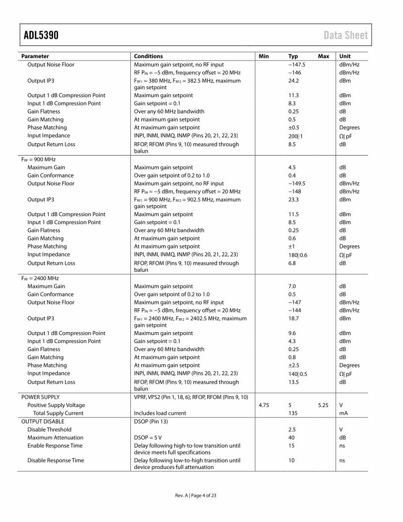
SPECIFICATIONS VS = 5 V, TA = 25°C, ZO = 50 Ω, FRF = 380 MHz, single-ended source drive to INPI and INPQ, and INMI and INMQ are ac-coupled to common, unless otherwise noted. 66.5 Ω termination resistors before ac-coupling capacitors on INPI and INPQ. The specifications refer to one active channel with the other channel input terminated in 50 Ω. The common-mode level for the gain control inputs is 0.5 V. A maximum gain setpoint of 1.0 refers to a differential gain control voltage of 0.5 V.
Table 1. Parameter Conditions Min Typ Max Unit OVERALL FUNCTION Frequency Range 20 2400 MHz
Gain Control Range Relative to maximum gain 35 dB GAIN CONTROL INTERFACE (I and Q) QBBP, QBBM, IBBM, IBBP (Pins 4, 5, 14, 15)
Gain Scaling 3.5 1/V Modulation Bandwidth 500 mV p-p, sinusoidal baseband input single-
ended 230 MHz
Second Harmonic Distortion 500 mV p-p, 1 MHz, sinusoidal baseband input differential
45 dBc
Third Harmonic Distortion 500 mV p-p, 1 MHz, sinusoidal baseband input differential
55 dBc
Step Response For gain from −15 dB to +5 dB 45 ns For gain from +5 dB to −15 dB 47 ns
FRF = 70 MHz Maximum Gain Maximum gain setpoint 4.6 dB Gain Conformance Over gain setpoint of 0.2 to 1.0 0.25 dB Output Noise Floor Maximum gain setpoint, no RF input −149 dBm/Hz RF PIN = −5 dBm, frequency offset = 20 MHz −146 dBm/Hz Output IP3 FRF1 = 70 MHz, FRF2 = 72.5 MHz, maximum gain
setpoint 23 dBm
Output 1 dB Compression Point Maximum gain setpoint 10.7 dBm Input 1 dB Compression Point Gain setpoint = 0.1 6.7 dBm Gain Flatness Over any 60 MHz bandwidth 0.25 dB Gain Matching At maximum gain setpoint 0.5 dB Phase Matching At maximum gain setpoint ±0.25 Degrees Input Impedance INPI, INMI, INMQ, INMP (Pins 20, 21, 22, 23) 250||1 Ω||pF Output Return Loss RFOP, RFOM (Pins 9, 10) measured through
balun 9.7 dB
FRF = 140 MHz Maximum Gain Maximum gain setpoint 4.5 dB Gain Conformance Over gain setpoint of 0.2 to 1.0 0.25 dB Output Noise Floor Maximum gain setpoint, no RF input −144 dBm/Hz RF PIN = −5 dBm, frequency offset = 20 MHz −145 dBm/Hz Output IP3 FRF1 = 140 MHz, FRF2 = 142.5 MHz, maximum
gain setpoint 24.4 dBm
Output 1 dB Compression Point Maximum gain setpoint 11 dBm Input 1 dB Compression Point Gain setpoint = 0.1 7.1 dBm Gain Flatness Over any 60 MHz bandwidth 0.25 dB Gain Matching At maximum gain setpoint 0.5 dB Phase Matching At maximum gain setpoint ±0.25 Degrees Input Impedance INPI, INMI, INMQ, INMP (Pins 20, 21, 22, 23) 250||1 Ω||pF Output Return Loss RFOP, RFOM (Pins 9, 10) measured through
balun 9.6 dB
FRF = 380 MHz Maximum Gain Maximum gain setpoint 4.1 dB Gain Conformance Over gain setpoint of 0.2 to 1.0 0.25 dB
ADL5390 Data Sheet
Rev. A | Page 4 of 23
Parameter Conditions Min Typ Max Unit Output Noise Floor Maximum gain setpoint, no RF input −147.5 dBm/Hz RF PIN = −5 dBm, frequency offset = 20 MHz −146 dBm/Hz Output IP3 FRF1 = 380 MHz, FRF2 = 382.5 MHz, maximum
gain setpoint 24.2 dBm
Output 1 dB Compression Point Maximum gain setpoint 11.3 dBm Input 1 dB Compression Point Gain setpoint = 0.1 8.3 dBm Gain Flatness Over any 60 MHz bandwidth 0.25 dB Gain Matching At maximum gain setpoint 0.5 dB Phase Matching At maximum gain setpoint ±0.5 Degrees Input Impedance INPI, INMI, INMQ, INMP (Pins 20, 21, 22, 23) 200||1 Ω||pF Output Return Loss RFOP, RFOM (Pins 9, 10) measured through
balun 8.5 dB
FRF = 900 MHz Maximum Gain Maximum gain setpoint 4.5 dB Gain Conformance Over gain setpoint of 0.2 to 1.0 0.4 dB Output Noise Floor Maximum gain setpoint, no RF input −149.5 dBm/Hz RF PIN = −5 dBm, frequency offset = 20 MHz −148 dBm/Hz Output IP3 FRF1 = 900 MHz, FRF2 = 902.5 MHz, maximum
gain setpoint 23.3 dBm
Output 1 dB Compression Point Maximum gain setpoint 11.5 dBm Input 1 dB Compression Point Gain setpoint = 0.1 8.5 dBm Gain Flatness Over any 60 MHz bandwidth 0.25 dB Gain Matching At maximum gain setpoint 0.6 dB Phase Matching At maximum gain setpoint ±1 Degrees Input Impedance INPI, INMI, INMQ, INMP (Pins 20, 21, 22, 23) 180||0.6 Ω||pF Output Return Loss RFOP, RFOM (Pins 9, 10) measured through
balun 6.8 dB
FRF = 2400 MHz Maximum Gain Maximum gain setpoint 7.0 dB Gain Conformance Over gain setpoint of 0.2 to 1.0 0.5 dB Output Noise Floor Maximum gain setpoint, no RF input −147 dBm/Hz RF PIN = −5 dBm, frequency offset = 20 MHz −144 dBm/Hz Output IP3 FRF1 = 2400 MHz, FRF2 = 2402.5 MHz, maximum
gain setpoint 18.7 dBm
Output 1 dB Compression Point Maximum gain setpoint 9.6 dBm Input 1 dB Compression Point Gain setpoint = 0.1 4.3 dBm Gain Flatness Over any 60 MHz bandwidth 0.25 dB Gain Matching At maximum gain setpoint 0.8 dB Phase Matching At maximum gain setpoint ±2.5 Degrees Input Impedance INPI, INMI, INMQ, INMP (Pins 20, 21, 22, 23) 140||0.5 Ω||pF Output Return Loss RFOP, RFOM (Pins 9, 10) measured through
balun 13.5 dB
POWER SUPPLY VPRF, VPS2 (Pin 1, 18, 6); RFOP, RFOM (Pins 9, 10) Positive Supply Voltage 4.75 5 5.25 V
Total Supply Current Includes load current 135 mA OUTPUT DISABLE DSOP (Pin 13)
Disable Threshold 2.5 V Maximum Attenuation DSOP = 5 V 40 dB Enable Response Time Delay following high-to-low transition until
device meets full specifications 15 ns
Disable Response Time Delay following low-to-high transition until device produces full attenuation
10 ns
Data Sheet ADL5390
Rev. A | Page 5 of 23
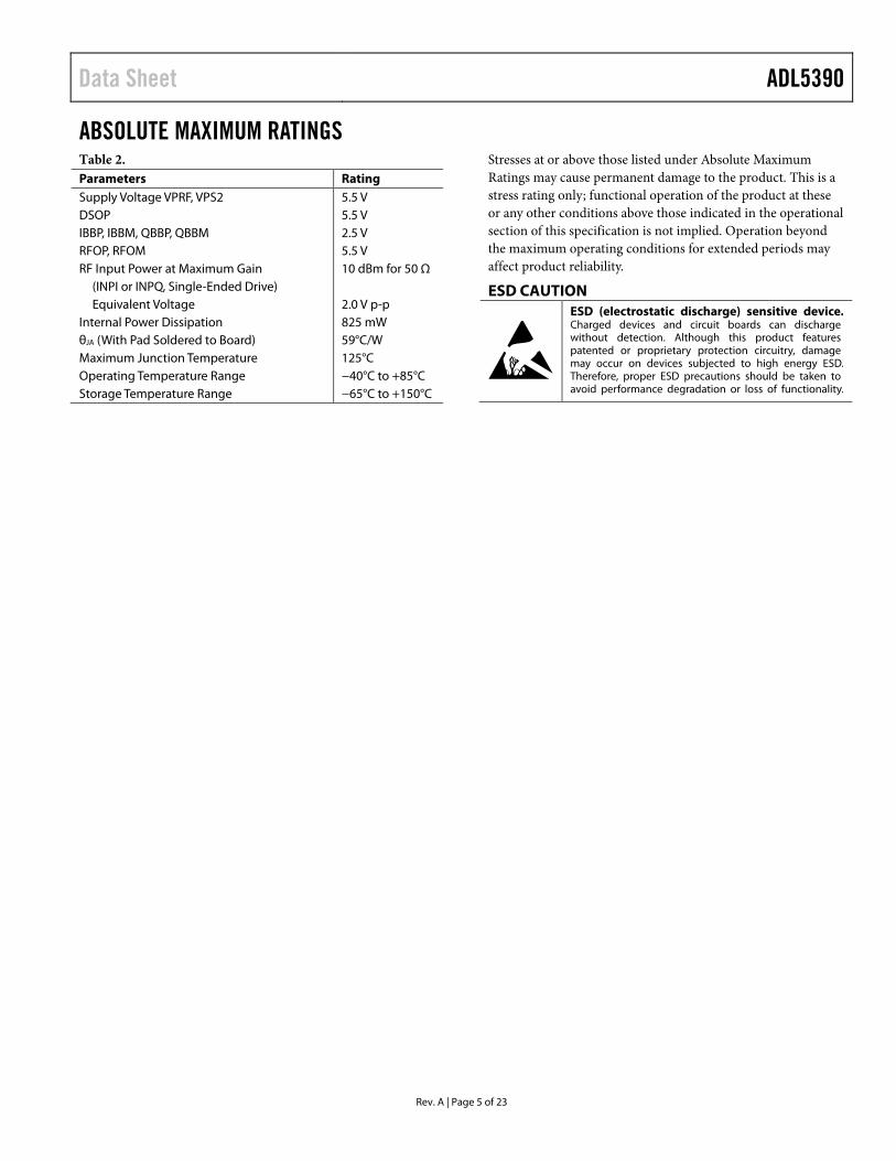
ABSOLUTE MAXIMUM RATINGS Table 2. Parameters Rating Supply Voltage VPRF, VPS2 5.5 V DSOP 5.5 V IBBP, IBBM, QBBP, QBBM 2.5 V RFOP, RFOM 5.5 V RF Input Power at Maximum Gain 10 dBm for 50 Ω
(INPI or INPQ, Single-Ended Drive) Equivalent Voltage 2.0 V p-p
Internal Power Dissipation 825 mW θJA (With Pad Soldered to Board) 59°C/W Maximum Junction Temperature 125°C Operating Temperature Range −40°C to +85°C Storage Temperature Range −65°C to +150°C
Stresses at or above those listed under Absolute Maximum Ratings may cause permanent damage to the product. This is a stress rating only; functional operation of the product at these or any other conditions above those indicated in the operational section of this specification is not implied. Operation beyond the maximum operating conditions for extended periods may affect product reliability.
ESD CAUTION
ADL5390 Data Sheet
Rev. A | Page 6 of 23
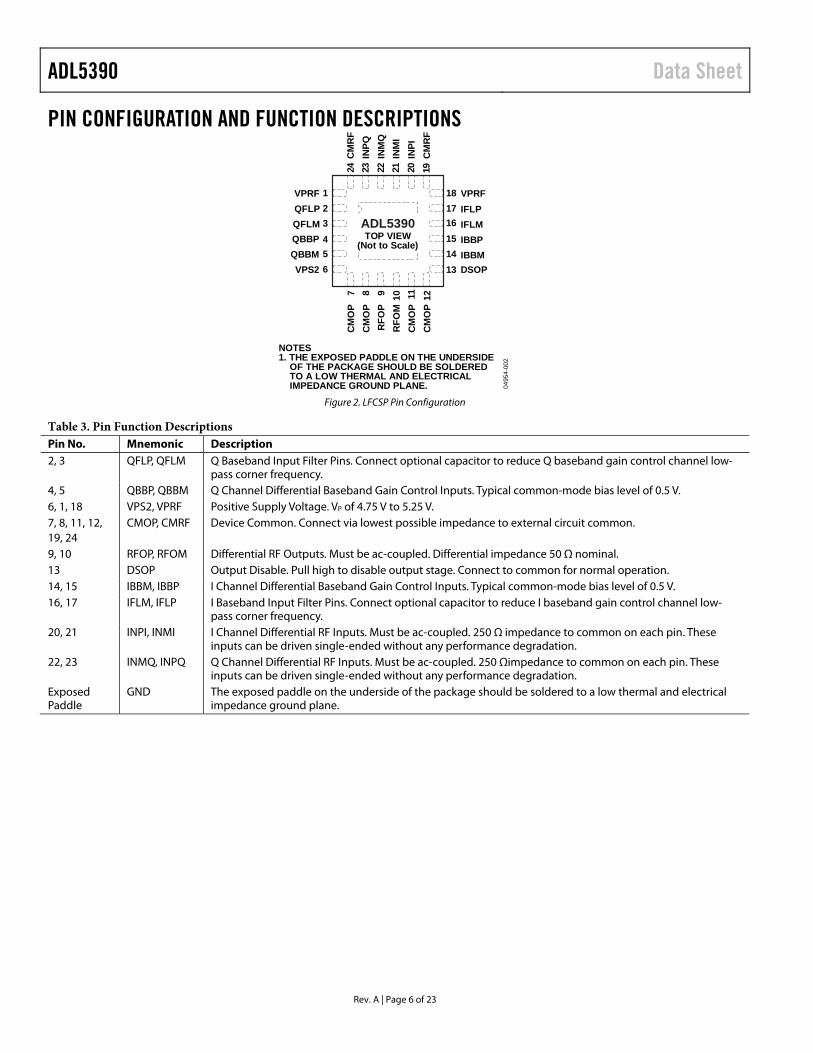
PIN CONFIGURATION AND FUNCTION DESCRIPTIONS
VPRFQFLPQFLMQBBPQBBMVPS2
VPRF
NOTES1. THE EXPOSED PADDLE ON THE UNDERSIDE OF THE PACKAGE SHOULD BE SOLDERED TO A LOW THERMAL AND ELECTRICAL IMPEDANCE GROUND PLANE.
IFLPIFLMIBBPIBBMDSOP
0495
4-00
2
CM
RF
INPQ
INM
QIN
MI
INPI
CM
RF
CM
OP
CM
OP
RFO
PR
FOM
CM
OP
CM
OP
21
3456
181716151413
8 9 10 117 1220 1921222324
ADL5390TOP VIEW
(Not to Scale)
Figure 2. LFCSP Pin Configuration
Table 3. Pin Function Descriptions Pin No. Mnemonic Description 2, 3 QFLP, QFLM Q Baseband Input Filter Pins. Connect optional capacitor to reduce Q baseband gain control channel low-
pass corner frequency. 4, 5 QBBP, QBBM Q Channel Differential Baseband Gain Control Inputs. Typical common-mode bias level of 0.5 V. 6, 1, 18 VPS2, VPRF Positive Supply Voltage. VP of 4.75 V to 5.25 V. 7, 8, 11, 12, 19, 24
CMOP, CMRF Device Common. Connect via lowest possible impedance to external circuit common.
9, 10 RFOP, RFOM Differential RF Outputs. Must be ac-coupled. Differential impedance 50 Ω nominal. 13 DSOP Output Disable. Pull high to disable output stage. Connect to common for normal operation. 14, 15 IBBM, IBBP I Channel Differential Baseband Gain Control Inputs. Typical common-mode bias level of 0.5 V. 16, 17 IFLM, IFLP I Baseband Input Filter Pins. Connect optional capacitor to reduce I baseband gain control channel low-
pass corner frequency. 20, 21 INPI, INMI I Channel Differential RF Inputs. Must be ac-coupled. 250 Ω impedance to common on each pin. These
inputs can be driven single-ended without any performance degradation. 22, 23 INMQ, INPQ Q Channel Differential RF Inputs. Must be ac-coupled. 250 Ωimpedance to common on each pin. These
inputs can be driven single-ended without any performance degradation. Exposed Paddle
GND The exposed paddle on the underside of the package should be soldered to a low thermal and electrical impedance ground plane.
Data Sheet ADL5390
Rev. A | Page 7 of 23
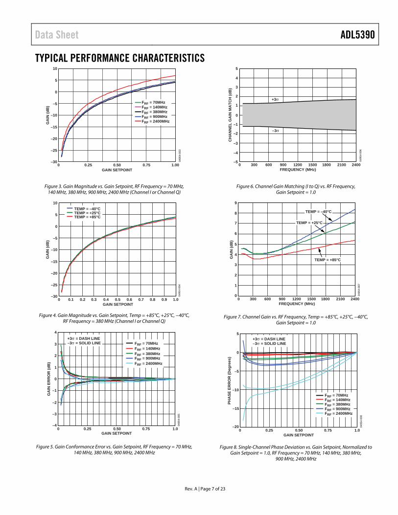
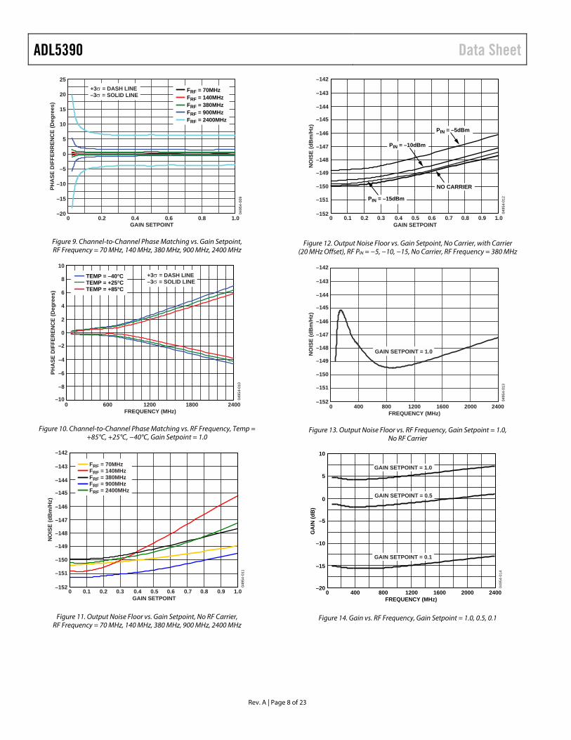
TYPICAL PERFORMANCE CHARACTERISTICS 10
5
0
–5
–10
–15
–20
–25
–300.250 0.50 0.75 1.00
GA
IN (d
B)
GAIN SETPOINT
0495
4-00
3
FRF = 70MHzFRF = 140MHzFRF = 380MHzFRF = 900MHzFRF = 2400MHz
Figure 3. Gain Magnitude vs. Gain Setpoint, RF Frequency = 70 MHz, 140 MHz, 380 MHz, 900 MHz, 2400 MHz (Channel I or Channel Q)
10
5
0
–5
–10
–15
–20
–25
–300 0.1 0.2 0.3 0.4 0.5 0.6 0.7 0.8 0.9 1.0
GA
IN (d
B)
GAIN SETPOINT
TEMP = –40°CTEMP = +25°CTEMP = +85°C
0495
4-00
4
Figure 4. Gain Magnitude vs. Gain Setpoint, Temp = +85°C, +25°C, −40°C,
RF Frequency = 380 MHz (Channel I or Channel Q)
0 0.25 0.50 0.75 1.0
4
3
2
1
0
–1
–2
–3
–4
GA
IN E
RR
OR
(dB
)
GAIN SETPOINT
FRF = 70MHzFRF = 140MHzFRF = 380MHzFRF = 900MHzFRF = 2400MHz
0495
4-00
5
+3σ = DASH LINE–3σ = SOLID LINE
Figure 5. Gain Conformance Error vs. Gain Setpoint, RF Frequency = 70 MHz, 140 MHz, 380 MHz, 900 MHz, 2400 MHz
5
4
3
2
1
0
–1
–2
–3
–4
–50 300 600 900 1200 1500 1800 2100 2400
CH
AN
NEL
GA
IN M
ATC
H (d
B)
FREQUENCY (MHz)
+3σ
–3σ
0495
4-00
6
Figure 6. Channel Gain Matching (I to Q) vs. RF Frequency, Gain Setpoint = 1.0
0 300 600 900 1200 1500 1800 2100 2400
9
8
7
6
5
4
3
2
1
0
GA
IN (d
B)
FREQUENCY (MHz)
TEMP = +85°C
TEMP = +25°C
TEMP = –40°C
0495
4-00
7
Figure 7. Channel Gain vs. RF Frequency, Temp = +85°C, +25°C, −40°C, Gain Setpoint = 1.0
0 0.25 0.50 0.75 1.0
5
0
–5
–10
–15
–20
PHA
SE E
RR
OR
(Deg
rees
)
GAIN SETPOINT
0495
4-00
8
FRF = 70MHzFRF = 140MHzFRF = 380MHzFRF = 900MHzFRF = 2400MHz
+3σ = DASH LINE–3σ = SOLID LINE
Figure 8. Single-Channel Phase Deviation vs. Gain Setpoint, Normalized to Gain Setpoint = 1.0, RF Frequency = 70 MHz, 140 MHz, 380 MHz,
900 MHz, 2400 MHz
ADL5390 Data Sheet
Rev. A | Page 8 of 23
25
20
15
10
5
0
–5
–10
–15
–200 0.2 0.4 0.6 0.8 1.0
PHA
SE D
IFFE
RR
ENC
E (D
egre
es)
GAIN SETPOINT
0495
4-00
9
FRF = 70MHzFRF = 140MHzFRF = 380MHzFRF = 900MHzFRF = 2400MHz
+3σ = DASH LINE–3σ = SOLID LINE
Figure 9. Channel-to-Channel Phase Matching vs. Gain Setpoint, RF Frequency = 70 MHz, 140 MHz, 380 MHz, 900 MHz, 2400 MHz
10
8
6
4
2
0
–2
–4
–6
–8
–10
PHA
SE D
IFFE
REN
CE
(Deg
rees
)
0 600 1200 1800 2400FREQUENCY (MHz)
TEMP = –40°CTEMP = +25°CTEMP = +85°C
0495
4-01
0
+3σ = DASH LINE–3σ = SOLID LINE
Figure 10. Channel-to-Channel Phase Matching vs. RF Frequency, Temp = +85°C, +25°C, −40°C, Gain Setpoint = 1.0
–142
–143
–144
–145
–146
–147
–148
–149
–150
–151
–152
NO
ISE
(dB
m/H
z)
0 0.1 0.2 0.3 0.4 0.5 0.6 0.7 0.8 0.9 1.0GAIN SETPOINT
0495
4-01
1
FRF = 70MHzFRF = 140MHzFRF = 380MHzFRF = 900MHzFRF = 2400MHz
Figure 11. Output Noise Floor vs. Gain Setpoint, No RF Carrier, RF Frequency = 70 MHz, 140 MHz, 380 MHz, 900 MHz, 2400 MHz
NO CARRIER
PIN = –15dBm
PIN = –10dBm
PIN = –5dBm
–142
–143
–144
–145
–146
–147
–148
–149
–150
–151
–152
NO
ISE
(dB
m/H
z)
0 0.1 0.2 0.3 0.4 0.5 0.6 0.7 0.8 0.9 1.0GAIN SETPOINT
0495
4-01
2
Figure 12. Output Noise Floor vs. Gain Setpoint, No Carrier, with Carrier (20 MHz Offset), RF PIN = −5, −10, −15, No Carrier, RF Frequency = 380 MHz
0495
4-01
3
–142
–143
–144
–145
–146
–147
–148
–149
–150
–151
–152
NO
ISE
(dB
m/H
z)
0 400 800 1200 1600 2000 2400
GAIN SETPOINT = 1.0
FREQUENCY (MHz)
Figure 13. Output Noise Floor vs. RF Frequency, Gain Setpoint = 1.0, No RF Carrier
–20
–15
–10
–5
0
5
10
0 400 800 1200 1600 2000 2400FREQUENCY (MHz)
GA
IN(d
B)
0495
4-01
4
GAIN SETPOINT = 1.0
GAIN SETPOINT = 0.5
GAIN SETPOINT = 0.1
Figure 14. Gain vs. RF Frequency, Gain Setpoint = 1.0, 0.5, 0.1
Data Sheet ADL5390
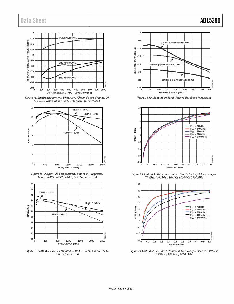
Rev. A | Page 9 of 23
0
–10
–20
–30
–40
–50
–60
–70
–80
–90
–1000 100 200 300 400 500 600 700 800 900 1000
RF
OU
TPU
T SI
DEB
AN
D P
OW
ER (d
Bm
) FUNDAMENTAL
2ND HARMONIC
3RD HARMONIC
DIFF. BASEBAND INPUT LEVEL (mV p-p)
0495
4-01
5
Figure 15. Baseband Harmonic Distortion, (Channel I and Channel Q),
RF PIN = −5 dBm, (Balun and Cable Losses Not Included)
0 400 800 1200 1600 2000 2400
12
11
10
9
8
7
6
FREQUENCY (MHz)
OP1
dB (d
Bm
)
TEMP = –40°C
TEMP = +25°C
TEMP = +85°C
0495
4-01
6
Figure 16. Output 1 dB Compression Point vs. RF Frequency, Temp = +85°C, +25°C, −40°C, Gain Setpoint = 1.0
0 400 800 1200 1600 2000 2400
30
28
26
24
22
20
18
16
14
12
10
TEMP = –40°C
TEMP = +25°C
TEMP = +85°C
FREQUENCY (MHz)
OIP
3 (d
Bm
)
0495
4-01
7
Figure 17. Output IP3 vs. RF Frequency, Temp = +85°C, +25°C, −40°C, Gain Setpoint = 1.0
0 50 100 150 200 250 300 350 400
0
–5
–10
–15
–20
–25
–30
–35
1V p-p BASEBAND INPUT
500mV p-p BASEBAND INPUT
250mV p-p BASEBAND INPUT
BB FREQUENCY (MHz)
SID
EBA
ND
PO
WER
(dB
m)
0495
4-01
8
Figure 18. IQ Modulation Bandwidth vs. Baseband Magnitude
0 0.1 0.2 0.3 0.4 0.5 0.6 0.7 0.8 0.9 1.0
15
10
5
0
–5
–10
–15
–20
–25
GAIN SETPOINT
OP1
dB (d
Bm
)
0495
4-01
9
FRF = 70MHzFRF = 140MHzFRF = 380MHzFRF = 900MHzFRF = 2400MHz
Figure 19. Output 1 dB Compression vs. Gain Setpoint, RF Frequency =
70 MHz, 140 MHz, 380 MHz, 900 MHz, 2400 MHz
0 0.1 0.2 0.3 0.4 0.5 0.6 0.7 0.8 0.9 1.0
15
10
5
0
–5
–10
–15
20
25
30
OIP
3 (d
Bm
)
GAIN SETPOINT
0495
4-02
0
FRF = 70MHzFRF = 140MHzFRF = 380MHzFRF = 900MHzFRF = 2400MHz
Figure 20. Output IP3 vs. Gain Setpoint, RF Frequency = 70 MHz, 140 MHz,
380 MHz, 900 MHz, 2400 MHz
ADL5390 Data Sheet
Rev. A | Page 10 of 23
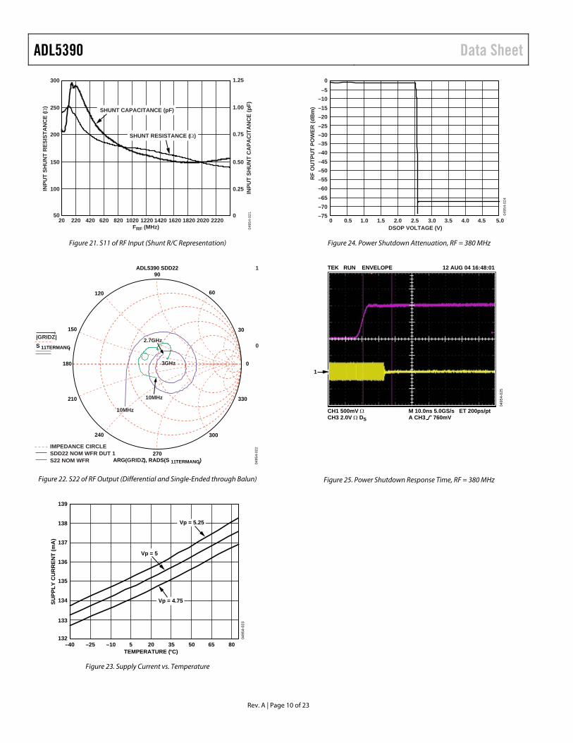
20 220 420 620 820 1020 1220 1420 1620 1820 2020 2220
300
250
200
150
100
50
FRF (MHz)
INPU
T SH
UN
T R
ESIS
TAN
CE
()
0495
4-02
1
1.25
1.00
0.75
0.50
0.25
0
INPU
T SH
UN
T C
APA
CIT
AN
CE
(pF)
SHUNT RESISTANCE ()
SHUNT CAPACITANCE (pF)
Figure 21. S11 of RF Input (Shunt R/C Representation)
|GRIDZ|S 11TERMANGI
0
1
0495
4-02
2
0180
30
330
60
ADL5390 SDD2290
270ARG(GRIDZ), RADS(S 11TERMANGI)
300
120
240
150
210
IMPEDANCE CIRCLESDD22 NOM WFR DUT 1S22 NOM WFR
10MHz
3GHz
2.7GHz
10MHz
Figure 22. S22 of RF Output (Differential and Single-Ended through Balun)
139
138
137
136
135
134
133
132–40 –25 –10 5 20 35 50 65 80
SUPP
LY C
UR
REN
T (m
A)
TEMPERATURE (°C)
0495
4-02
3
Vp = 5.25
Vp = 4.75
Vp = 5
Figure 23. Supply Current vs. Temperature
0 0.5 1.0 1.5 2.0 2.5 3.0 3.5 4.0 4.5 5.0
0–5
–10–15–20–25–30–35–40–45–50–55–60–65–70–75
DSOP VOLTAGE (V)
RF
OU
TPU
T PO
WER
(dB
m)
0495
4-02
4
Figure 24. Power Shutdown Attenuation, RF = 380 MHz
TEK RUN ENVELOPE 12 AUG 04 16:48:01
CH1 500mV CH3 2.0V DS
M 10.0ns 5.0GS/s ET 200ps/ptA CH3 760mV
1
0495
4-02
5
Figure 25. Power Shutdown Response Time, RF = 380 MHz
Data Sheet ADL5390
Rev. A | Page 11 of 23
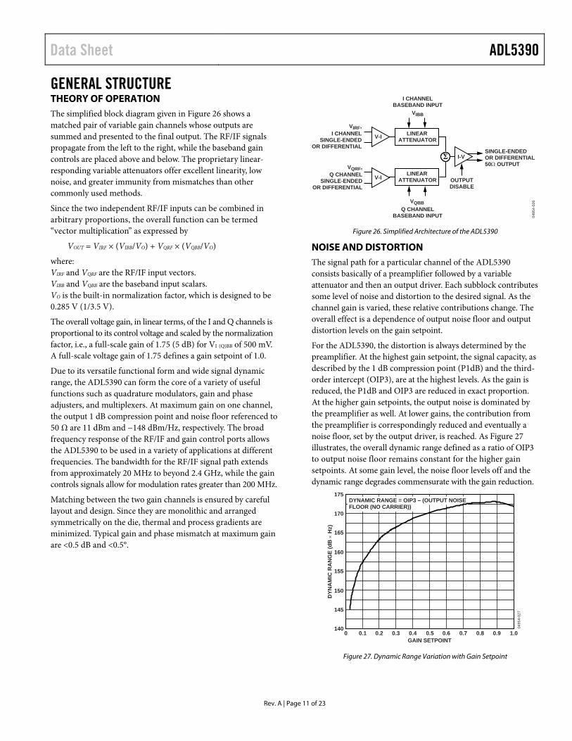
GENERAL STRUCTURE THEORY OF OPERATION The simplified block diagram given in Figure 26 shows a matched pair of variable gain channels whose outputs are summed and presented to the final output. The RF/IF signals propagate from the left to the right, while the baseband gain controls are placed above and below. The proprietary linear-responding variable attenuators offer excellent linearity, low noise, and greater immunity from mismatches than other commonly used methods.
Since the two independent RF/IF inputs can be combined in arbitrary proportions, the overall function can be termed “vector multiplication” as expressed by
VOUT = VIRF × (VIBB/VO) + VQRF × (VQBB/VO)
where: VIRF and VQRF are the RF/IF input vectors. VIBB and VQBB are the baseband input scalars. VO is the built-in normalization factor, which is designed to be 0.285 V (1/3.5 V).
The overall voltage gain, in linear terms, of the I and Q channels is proportional to its control voltage and scaled by the normalization factor, i.e., a full-scale gain of 1.75 (5 dB) for VI (Q)BB of 500 mV. A full-scale voltage gain of 1.75 defines a gain setpoint of 1.0.
Due to its versatile functional form and wide signal dynamic range, the ADL5390 can form the core of a variety of useful functions such as quadrature modulators, gain and phase adjusters, and multiplexers. At maximum gain on one channel, the output 1 dB compression point and noise floor referenced to 50 Ω are 11 dBm and −148 dBm/Hz, respectively. The broad frequency response of the RF/IF and gain control ports allows the ADL5390 to be used in a variety of applications at different frequencies. The bandwidth for the RF/IF signal path extends from approximately 20 MHz to beyond 2.4 GHz, while the gain controls signals allow for modulation rates greater than 200 MHz.
Matching between the two gain channels is ensured by careful layout and design. Since they are monolithic and arranged symmetrically on the die, thermal and process gradients are minimized. Typical gain and phase mismatch at maximum gain are <0.5 dB and <0.5°.
0495
4-02
6
LINEARATTENUATOR
LINEARATTENUATOR
I-V
VQBBQ CHANNEL
BASEBAND INPUT
VIRF,I CHANNEL
SINGLE-ENDEDOR DIFFERENTIAL
VIBB
OUTPUTDISABLE
SINGLE-ENDEDOR DIFFERENTIAL50Ω OUTPUTVQRF,
Q CHANNELSINGLE-ENDED
OR DIFFERENTIAL
I CHANNELBASEBAND INPUT
V-I
V-I
Figure 26. Simplified Architecture of the ADL5390
NOISE AND DISTORTION The signal path for a particular channel of the ADL5390 consists basically of a preamplifier followed by a variable attenuator and then an output driver. Each subblock contributes some level of noise and distortion to the desired signal. As the channel gain is varied, these relative contributions change. The overall effect is a dependence of output noise floor and output distortion levels on the gain setpoint.
For the ADL5390, the distortion is always determined by the preamplifier. At the highest gain setpoint, the signal capacity, as described by the 1 dB compression point (P1dB) and the third-order intercept (OIP3), are at the highest levels. As the gain is reduced, the P1dB and OIP3 are reduced in exact proportion. At the higher gain setpoints, the output noise is dominated by the preamplifier as well. At lower gains, the contribution from the preamplifier is correspondingly reduced and eventually a noise floor, set by the output driver, is reached. As Figure 27 illustrates, the overall dynamic range defined as a ratio of OIP3 to output noise floor remains constant for the higher gain setpoints. At some gain level, the noise floor levels off and the dynamic range degrades commensurate with the gain reduction.
175
170
165
160
155
150
145
140
DYN
AM
IC R
AN
GE
(dB×
Hz)
0 0.1 0.2 0.3 0.4 0.5 0.6 0.7 0.8 0.9 1.0GAIN SETPOINT
0495
4-02
7
DYNAMIC RANGE = OIP3 – (OUTPUT NOISEFLOOR (NO CARRIER))
Figure 27. Dynamic Range Variation with Gain Setpoint
ADL5390 Data Sheet
Rev. A | Page 12 of 23
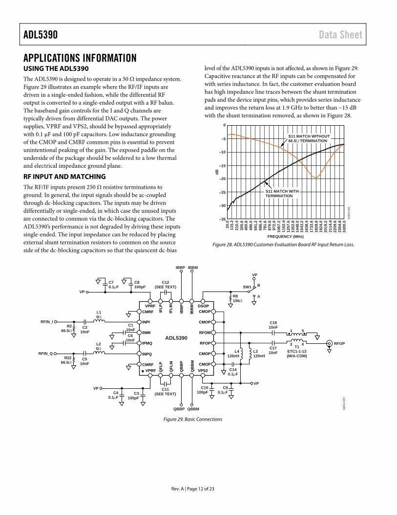
APPLICATIONS INFORMATION USING THE ADL5390 The ADL5390 is designed to operate in a 50 Ω impedance system. Figure 29 illustrates an example where the RF/IF inputs are driven in a single-ended fashion, while the differential RF output is converted to a single-ended output with a RF balun. The baseband gain controls for the I and Q channels are typically driven from differential DAC outputs. The power supplies, VPRF and VPS2, should be bypassed appropriately with 0.1 μF and 100 pF capacitors. Low inductance grounding of the CMOP and CMRF common pins is essential to prevent unintentional peaking of the gain. The exposed paddle on the underside of the package should be soldered to a low thermal and electrical impedance ground plane.
RF INPUT AND MATCHING The RF/IF inputs present 250 Ω resistive terminations to ground. In general, the input signals should be ac-coupled through dc-blocking capacitors. The inputs may be driven differentially or single-ended, in which case the unused inputs are connected to common via the dc-blocking capacitors. The ADL5390’s performance is not degraded by driving these inputs single-ended. The input impedance can be reduced by placing external shunt termination resistors to common on the source side of the dc-blocking capacitors so that the quiescent dc-bias
level of the ADL5390 inputs is not affected, as shown in Figure 29. Capacitive reactance at the RF inputs can be compensated for with series inductance. In fact, the customer evaluation board has high impedance line traces between the shunt termination pads and the device input pins, which provides series inductance and improves the return loss at 1.9 GHz to better than −15 dB with the shunt termination removed, as shown in Figure 28.
S11 MATCH WITHOUT66.5 TERMINATION
S11 MATCH WITHTERMINATION
0
–5
–10
–15
–20
–25
–30
–35dB
20.0
305.
6
591.
2
876.
8
1162
.4
1448
.0
1733
.6
2019
.2
2400
.0
115.
221
0.4
400.
849
6.0
686.
478
1.6
972.
010
67.2
1257
.613
52.8
1543
.216
38.4
1828
.819
24.0
2114
.422
09.6
2304
.8
FREQUENCY (MHz)
0495
4-02
8
Figure 28. ADL5390 Customer Evaluation Board RF Input Return Loss.
0495
4-02
9
C12(SEE TEXT)
C11(SEE TEXT)
C8100pF
VP
C70.1F
VPC4
0.1F
B
A
SW1
R810k
VP
IBBMIBBP
QBBP QBBM
L20
C510nF
RFIN_QR22
66.5
L10
C210nF
RFIN_IR2
66.5C1
10nFC6
10nF
L4120nH
L3120nH
C140.1F
C10100pF
C90.1F
VP
C1710nF
C1810nF
RFOP
1 5
3 4T1ETC1-1-13(M/A-COM)
IBB
P
IBB
M
VPS2
DSOP
QB
BP
QB
BM
VPRFCMRF
INMI
IPMQ
CMOP
CMOP
RFOM
RFOP
QFL
P
QFL
M
CMOP
CMOPCMRFVPRF
IFLP
IFLM
ADL5390
INPI
INPQ
C3100pF
Figure 29. Basic Connections
Data Sheet ADL5390
Rev. A | Page 13 of 23
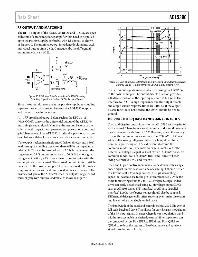
RF OUTPUT AND MATCHING The RF/IF outputs of the ADL5390, RFOP and RFOM, are open collectors of a transimpedance amplifier that need to be pulled up to the positive supply, preferably with RF chokes, as shown in Figure 30. The nominal output impedance looking into each individual output pin is 25 Ω. Consequently, the differential output impedance is 50 Ω.
0495
4-03
050DIFFERENTIAL
10pF1:1 RF
OUTPUTRFOM
RFOP
RT
RT
120nH
10pF
VP
GM±ISIG
0.1F
Figure 30. RF Output Interface to the ADL5390 Showing
Coupling Capacitors, Pull-Up RF Chokes, and Balun
Since the output dc levels are at the positive supply, ac-coupling capacitors are usually needed between the ADL5390 outputs and the next stage in the system.
A 1:1 RF broadband output balun, such as the ETC1-1-13 (M/A-COM), converts the differential output of the ADL5390 into a single-ended signal. Note that the loss and balance of the balun directly impact the apparent output power, noise floor, and gain/phase errors of the ADL5390. In critical applications, narrow-band baluns with low loss and superior balance are recommended.
If the output is taken in a single-ended fashion directly into a 50 Ω load through a coupling capacitor, there will be an impedance mismatch. This can be resolved with a 1:2 balun to convert the single-ended 25 Ω output impedance to 50 Ω. If loss of signal swing is not critical, a 25 Ω back termination in series with the output pin can also be used. The unused output pin must still be pulled up to the positive supply. The user may load it through a coupling capacitor with a dummy load to preserve balance. The mismatched gain of the ADL5390 when the output is single-ended varies slightly with dummy load value, as shown in Figure 31.
10
–10
–4
–2
0
2
4
6
8
10 100 1000 10000
0495
4-04
3
FREQUENCY (MHz)
GA
IN (d
B)
RL2 = OPEN
RL2 = 50
RL2 = SHORT
RL = 50
Figure 31. Gain of the ADL5390 Using a Single-Ended Output with Different
Dummy Loads, RL2 on the Unused Output, Gain Setpoint = 1.0
The RF output signal can be disabled by raising the DSOP pin to the positive supply. The output disable function provides >40 dB attenuation of the input signal, even at full gain. The interface to DSOP is high impedance and the output disable and output enable response times are <100 ns. If the output disable function is not needed, the DSOP should be tied to ground.
DRIVING THE I-Q BASEBAND GAIN CONTROLS The I and Q gain control inputs to the ADL5390 set the gain for each channel. These inputs are differential and should normally have a common-mode level of 0.5 V. However, when differentially driven, the common mode can vary from 250 mV to 750 mV while still allowing full gain control. Each input pair has a nominal input swing of ±0.5 V differential around the common-mode level. The maximum gain is achieved if the differential voltage is equal to +500 mV or −500 mV. So with a common-mode level of 500 mV, IBBP and IBBM will each swing between 250 mV and 750 mV.
The I and Q gain control inputs can also be driven with a single-ended signal. In this case, one side of each input should be tied to a low noise 0.5 V voltage source (a 0.1 μF decoupling capacitor located close to the pin is recommended), while the other input swings from 0 V to 1 V. Low speed, single-ended drive can easily be achieved using 12-bit voltage output DACs such as AD8303 (serial SPI® interface) or AD8582 (parallel interface) DACs. A reference voltage should also be supplied. Differential drive generally offers superior even-order distortion and lower noise than single-ended drive.
The bandwidth of the baseband controls exceeds 200 MHz even at full-scale baseband drive. This allows for very fast gain modulation of the RF input signal. In cases where lower modulation band-widths are acceptable or desired, external filter capacitors can be connected across Pins IFLP to IFLM and Pins QFLP to QFLM to reduce the ingress of baseband noise and spurious signal into the control path.
ADL5390 Data Sheet
Rev. A | Page 14 of 23
The 3 dB bandwidth is set by choosing CFLT according to the following equation:
pF0.5nF10kHz45
dB3
externalCf
This equation has been verified for values of CFLT from 10 pF to 0.1 μF (bandwidth settings of approximately 4.5 kHz to 43 MHz).
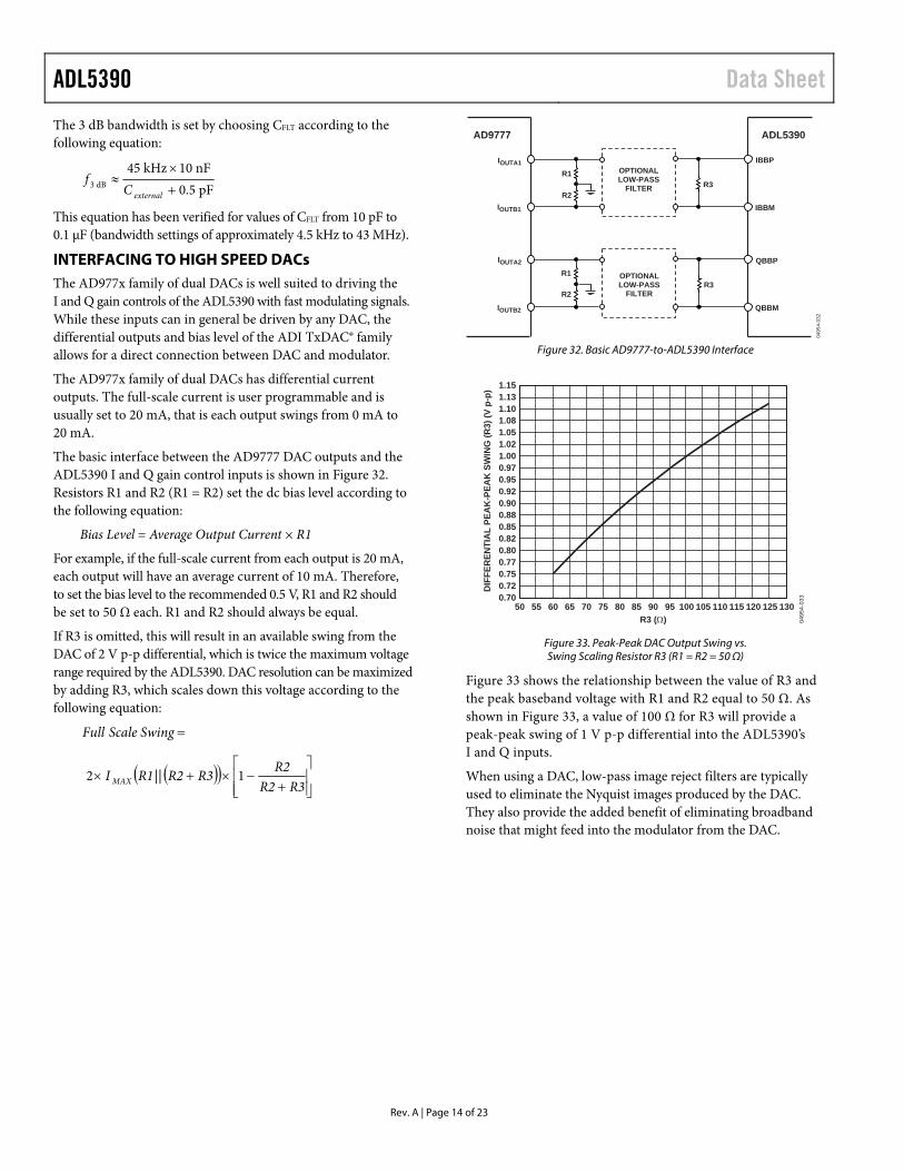
INTERFACING TO HIGH SPEED DACs The AD977x family of dual DACs is well suited to driving the I and Q gain controls of the ADL5390 with fast modulating signals. While these inputs can in general be driven by any DAC, the differential outputs and bias level of the ADI TxDAC® family allows for a direct connection between DAC and modulator.
The AD977x family of dual DACs has differential current outputs. The full-scale current is user programmable and is usually set to 20 mA, that is each output swings from 0 mA to 20 mA.
The basic interface between the AD9777 DAC outputs and the ADL5390 I and Q gain control inputs is shown in Figure 32. Resistors R1 and R2 (R1 = R2) set the dc bias level according to the following equation:
Bias Level = Average Output Current × R1
For example, if the full-scale current from each output is 20 mA, each output will have an average current of 10 mA. Therefore, to set the bias level to the recommended 0.5 V, R1 and R2 should be set to 50 Ω each. R1 and R2 should always be equal.
If R3 is omitted, this will result in an available swing from the DAC of 2 V p-p differential, which is twice the maximum voltage range required by the ADL5390. DAC resolution can be maximized by adding R3, which scales down this voltage according to the following equation:
SwingScaleFull
R3R2R2R3R2R1I MAX 1||2
OPTIONALLOW-PASS
FILTER
0495
4-03
2
R1
R2R3
IOUTB2
IOUTA2
QBBM
QBBP
IOUTB1
IOUTA1
IBBM
IBBP
AD9777 ADL5390
OPTIONALLOW-PASS
FILTER
R1
R2R3
Figure 32. Basic AD9777-to-ADL5390 Interface
R3 () 0495
4-03
3
13050 55 60 65 70 75 80 85 90 100 105 115 120110 12595
DIF
FER
ENTI
AL
PEA
K-P
EAK
SW
ING
(R3)
(V p
-p) 1.15
1.081.101.13
1.001.021.05
0.950.97
0.880.900.92
0.770.800.820.85
0.70
0.750.72
Figure 33. Peak-Peak DAC Output Swing vs. Swing Scaling Resistor R3 (R1 = R2 = 50 Ω)
Figure 33 shows the relationship between the value of R3 and the peak baseband voltage with R1 and R2 equal to 50 Ω. As shown in Figure 33, a value of 100 Ω for R3 will provide a peak-peak swing of 1 V p-p differential into the ADL5390’s I and Q inputs.
When using a DAC, low-pass image reject filters are typically used to eliminate the Nyquist images produced by the DAC. They also provide the added benefit of eliminating broadband noise that might feed into the modulator from the DAC.
Data Sheet ADL5390
Rev. A | Page 15 of 23
GENERALIZED MODULATOR The ADL5390 can be configured as a traditional IQ quadrature modulator or as a linear vector modulator by applying signals that are in quadrature to the RF/IF input channels. Since the quadrature generation is performed externally, its accuracy and bandwidth are determined by the user. The user-defined band-width is attractive for multioctave or lower IF applications where on-chip, high accuracy quadrature generation is traditionally difficult or impractical. The gain control pins (IBBP/M and QBBP/M) become the in-phase (I) and quadrature (Q) baseband inputs for the quadrature modulator and the gain/phase control for the vector modulator. The wide modulation bandwidths of the gain control interface allow for high fidelity baseband signals to be generated for the quadrature modulator and for high speed gain and phase adjustments to be generated for the vector modulator.
RF/IF signals can be introduce to the ADL5390 in quadrature by using a two-way 90° power splitter such as the Mini-Circuits QCN-12. Each output of an ideal 90° power splitter is 3 dB smaller than the input and has a 90° phase difference from the other output. In reality, the 90° power splitter will have its own insertion loss, which can be different for each output, causing a magnitude imbalance. Furthermore, quadrature output will not be maintained over a large frequency range, introducing a phase imbalance. The type of 90° power splitter that should be used for a particular application will be determined by the frequency, bandwidth, and accuracy needed. In some applications minor magnitude and phase imbalances can be adjusted for in the I/Q gain control inputs.
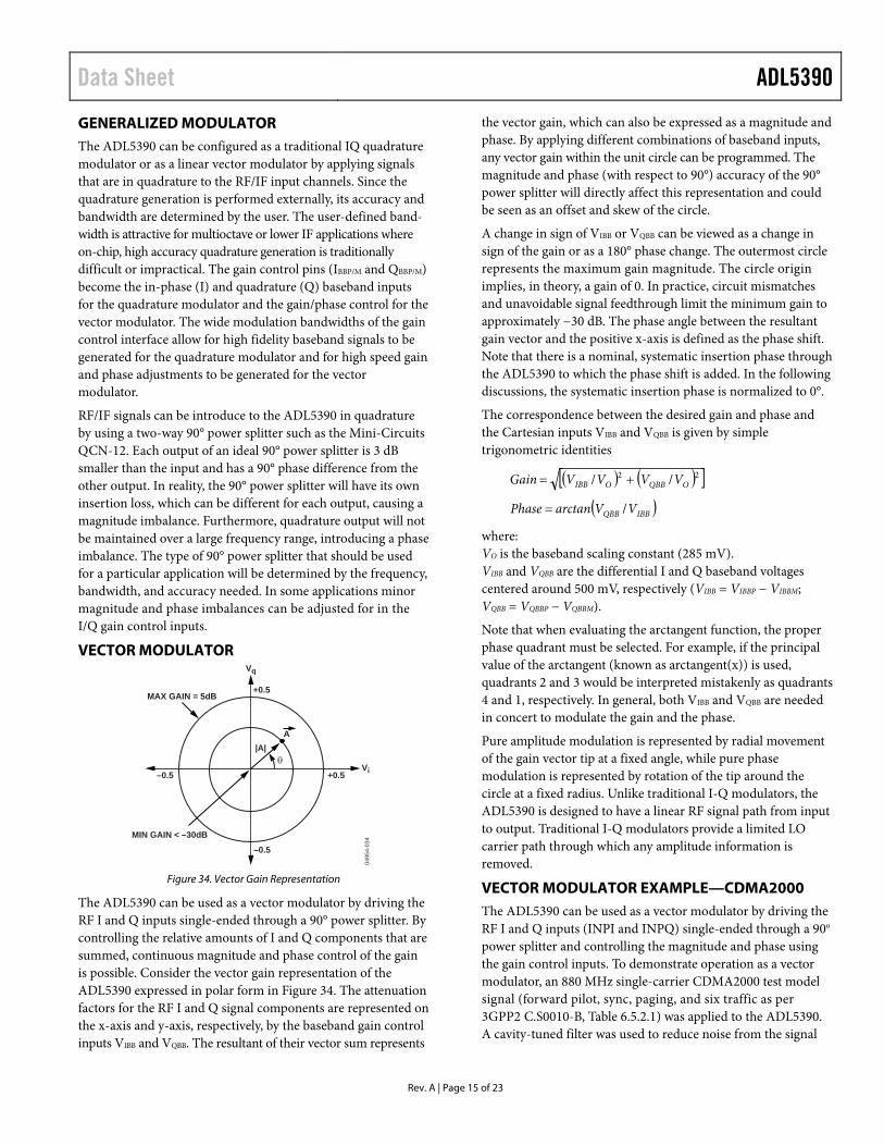
VECTOR MODULATOR
0495
4-03
4
|A|θ
A
+0.5–0.5
+0.5
–0.5
Vi
Vq
MIN GAIN < –30dB
MAX GAIN = 5dB
Figure 34. Vector Gain Representation
The ADL5390 can be used as a vector modulator by driving the RF I and Q inputs single-ended through a 90° power splitter. By controlling the relative amounts of I and Q components that are summed, continuous magnitude and phase control of the gain is possible. Consider the vector gain representation of the ADL5390 expressed in polar form in Figure 34. The attenuation factors for the RF I and Q signal components are represented on the x-axis and y-axis, respectively, by the baseband gain control inputs VIBB and VQBB. The resultant of their vector sum represents
the vector gain, which can also be expressed as a magnitude and phase. By applying different combinations of baseband inputs, any vector gain within the unit circle can be programmed. The magnitude and phase (with respect to 90°) accuracy of the 90° power splitter will directly affect this representation and could be seen as an offset and skew of the circle.
A change in sign of VIBB or VQBB can be viewed as a change in sign of the gain or as a 180° phase change. The outermost circle represents the maximum gain magnitude. The circle origin implies, in theory, a gain of 0. In practice, circuit mismatches and unavoidable signal feedthrough limit the minimum gain to approximately −30 dB. The phase angle between the resultant gain vector and the positive x-axis is defined as the phase shift. Note that there is a nominal, systematic insertion phase through the ADL5390 to which the phase shift is added. In the following discussions, the systematic insertion phase is normalized to 0°.
The correspondence between the desired gain and phase and the Cartesian inputs VIBB and VQBB is given by simple trigonometric identities
( ) ( )[ ]22 // OQBBOIBB VVVVGain +=
( )IBBQBB VVarctanPhase /=
where: VO is the baseband scaling constant (285 mV). VIBB and VQBB are the differential I and Q baseband voltages centered around 500 mV, respectively (VIBB = VIBBP − VIBBM; VQBB = VQBBP − VQBBM).
Note that when evaluating the arctangent function, the proper phase quadrant must be selected. For example, if the principal value of the arctangent (known as arctangent(x)) is used, quadrants 2 and 3 would be interpreted mistakenly as quadrants 4 and 1, respectively. In general, both VIBB and VQBB are needed in concert to modulate the gain and the phase.
Pure amplitude modulation is represented by radial movement of the gain vector tip at a fixed angle, while pure phase modulation is represented by rotation of the tip around the circle at a fixed radius. Unlike traditional I-Q modulators, the ADL5390 is designed to have a linear RF signal path from input to output. Traditional I-Q modulators provide a limited LO carrier path through which any amplitude information is removed.
VECTOR MODULATOR EXAMPLE—CDMA2000 The ADL5390 can be used as a vector modulator by driving the RF I and Q inputs (INPI and INPQ) single-ended through a 90o power splitter and controlling the magnitude and phase using the gain control inputs. To demonstrate operation as a vector modulator, an 880 MHz single-carrier CDMA2000 test model signal (forward pilot, sync, paging, and six traffic as per 3GPP2 C.S0010-B, Table 6.5.2.1) was applied to the ADL5390. A cavity-tuned filter was used to reduce noise from the signal
ADL5390 Data Sheet
Rev. A | Page 16 of 23
source being applied to the device. The 4.6 MHz pass band of this filter is apparent in the subsequent spectral plots.
Figure 35 shows the output signal spectrum for a programmed gain and phase of 5 dB and 45°. POUT is equal to 0 dBm and VIBB = VQBB = 0.353 V (centered around 500 mV), that is , VIBBP − VIBBM = VQBBP − VQBBM = 0.353 V. Adjacent channel power is measured in 30 kHz resolution bandwidth at 750 kHz and 1.98 MHz carrier offset. Noise floor is measured at ±4 MHz carrier offset in a 1 MHz resolution bandwidth.
1
CU2CU2
CU1
C0C0
Cl1Cl1
Cl2Cl2
CU1
0495
4-03
5
A
CENTER 880MHz 500kHz/ SPAN 5MHz
REF LVL5dBm0.7dB OFFSET
1AVG
MARKER 1 [T1]–14.38dBm880.00755511MHz
RBW 30kHzVWB 300kHzSWT 2s
RF ATT 20dBMIXER –10dBmUNIT dB
1 [T1] –14.38dBm880.00755511MHz
CH PWR
0
–70
–80
–90
–100
–60
–50
–40
–30
–20
–101 [T1] –14.38dBm 880.00755511MHzCH PWR 0.13dBmACP UP –62.00dBACP LOW –61.98dBALT1 UP –87.02dBALT1 LOW –87.04dB 1RM
EXT
Figure 35. Output Spectrum, Single-Carrier CDMA2000 Test Model at −5 dBm,
VI = VQ = 0.353 V, ACP Measured at 750 kHz and 1.98 MHz Carrier Offset, Input Signal–Filtered Using a Cavity-Tuned Filter (Pass Band = 4.6 MHz)
Holding the I and Q gain control voltages steady at 0.353 V, input power was swept. Figure 36 shows the resulting output power, noise floor, and adjacent channel power ratio. The noise floor is presented as noise in a 1 MHz bandwidth as defined by the 3GPP2 specification.
–30
–100
–90
–80
–70
–60
–50
–40
–30
–100
–90
–80
–70
–60
–50
–40
–30 –25 –20 –15 –10 –5 0 5
0495
4-04
4
OUTPUT POWER (dBm)
AC
P (d
Bc)
NO
ISE
(dB
m @
4M
Hz
Car
rier O
ffset
)
ACP: 750kHz OFFSET, 30kHz RBW
ACP: 1.98MHz OFFSET, 30kHz RBW
NOISE: 4MHz OFFSET, 1MHz RBW
Figure 36. Noise and ACP vs. Output Power, Single-Carrier CDMA2000 Test
Model, VI = VQ = 0.353, ACP Measured in 30 kHz RBW at ±750 kHz and ±1.98 MHz Carrier Offset, Noise Measured at ±4 MHz Carrier Offset
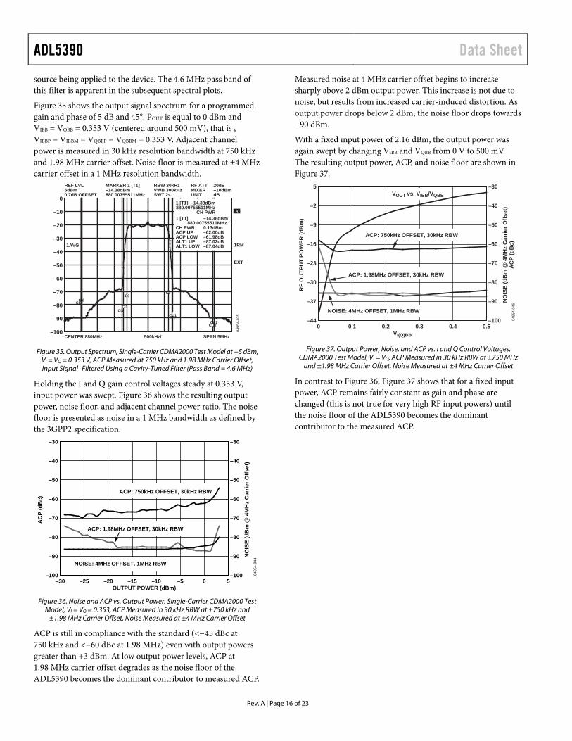
ACP is still in compliance with the standard (<−45 dBc at 750 kHz and <−60 dBc at 1.98 MHz) even with output powers greater than +3 dBm. At low output power levels, ACP at 1.98 MHz carrier offset degrades as the noise floor of the ADL5390 becomes the dominant contributor to measured ACP.
Measured noise at 4 MHz carrier offset begins to increase sharply above 2 dBm output power. This increase is not due to noise, but results from increased carrier-induced distortion. As output power drops below 2 dBm, the noise floor drops towards −90 dBm.
With a fixed input power of 2.16 dBm, the output power was again swept by changing VIBB and VQBB from 0 V to 500 mV. The resulting output power, ACP, and noise floor are shown in Figure 37.
5
–44
–37
–30
–23
–16
–9
–2
–30
–100
–90
–80
–70
–60
–50
–40
0 0.1 0.2 0.3 0.4 0.5
0495
4-04
5
VI(Q)BB
RF
OU
TPU
T PO
WER
(dB
m)
NO
ISE
(dB
m @
4M
Hz
Car
rier O
ffset
)A
CP
(dB
c)
VOUT vs. VIBB/VQBB
ACP: 750kHz OFFSET, 30kHz RBW
NOISE: 4MHz OFFSET, 1MHz RBW
ACP: 1.98MHz OFFSET, 30kHz RBW
Figure 37. Output Power, Noise, and ACP vs. I and Q Control Voltages,
CDMA2000 Test Model, VI = VQ, ACP Measured in 30 kHz RBW at ±750 MHz and ±1.98 MHz Carrier Offset, Noise Measured at ±4 MHz Carrier Offset
In contrast to Figure 36, Figure 37 shows that for a fixed input power, ACP remains fairly constant as gain and phase are changed (this is not true for very high RF input powers) until the noise floor of the ADL5390 becomes the dominant contributor to the measured ACP.
Data Sheet ADL5390
Rev. A | Page 17 of 23
QUADRATURE MODULATOR The ADL5390 can be used as a quadrature modulator by driving the RF I and Q inputs (INPI and INPQ) single-ended through a 90° phase splitter to serve as the LO input. I/Q modulation is applied to the baseband I and Q gain control inputs (IBBP/IBBM and QBBP/QBBM). A simplified schematic is shown in Figure 38.
0495
4-03
8
90° PHASESPLITTER
SUMPORT
TERMPORT
PORT 1
PORT 2
QCN-12
QB
BP
QB
BM
IBB
P
IBB
M
RFOM
RFOP
INPI
Q DATA
I DATA
INPQ
1 5
3 4 ROFP
LO IN
ADL5390
10nF
10nF
10nF
10nF
66.5
66.5
50
ETC1-1-13(M/A-COM)
Figure 38. Quadrature Modulator Application
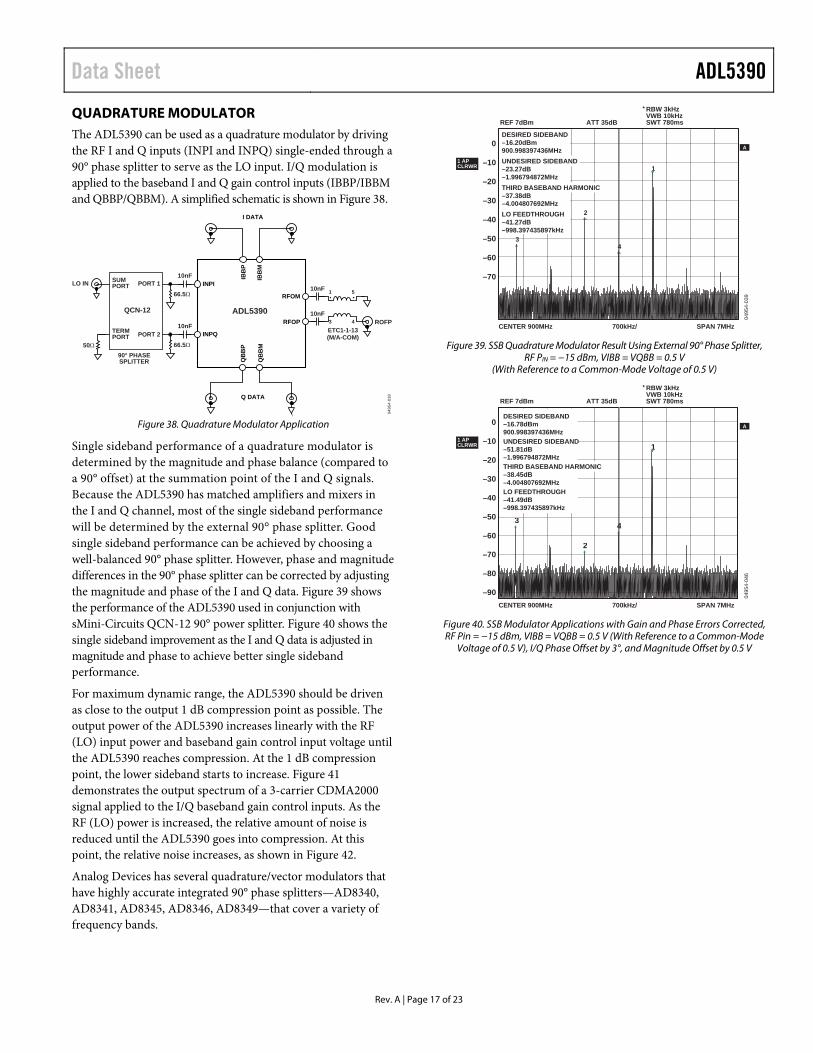
Single sideband performance of a quadrature modulator is determined by the magnitude and phase balance (compared to a 90° offset) at the summation point of the I and Q signals. Because the ADL5390 has matched amplifiers and mixers in the I and Q channel, most of the single sideband performance will be determined by the external 90° phase splitter. Good single sideband performance can be achieved by choosing a well-balanced 90° phase splitter. However, phase and magnitude differences in the 90° phase splitter can be corrected by adjusting the magnitude and phase of the I and Q data. Figure 39 shows the performance of the ADL5390 used in conjunction with sMini-Circuits QCN-12 90° power splitter. Figure 40 shows the single sideband improvement as the I and Q data is adjusted in magnitude and phase to achieve better single sideband performance.
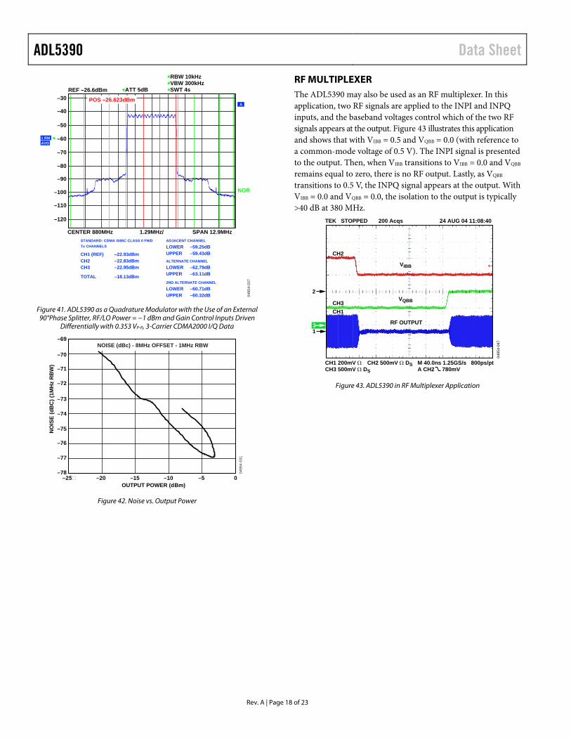
For maximum dynamic range, the ADL5390 should be driven as close to the output 1 dB compression point as possible. The output power of the ADL5390 increases linearly with the RF (LO) input power and baseband gain control input voltage until the ADL5390 reaches compression. At the 1 dB compression point, the lower sideband starts to increase. Figure 41 demonstrates the output spectrum of a 3-carrier CDMA2000 signal applied to the I/Q baseband gain control inputs. As the RF (LO) power is increased, the relative amount of noise is reduced until the ADL5390 goes into compression. At this point, the relative noise increases, as shown in Figure 42.
Analog Devices has several quadrature/vector modulators that have highly accurate integrated 90° phase splitters—AD8340, AD8341, AD8345, AD8346, AD8349—that cover a variety of frequency bands.
0495
4-03
9
-90
-80
1
2
34
A
CENTER 900MHz 700kHz/ SPAN 7MHz
REF 7dBm ATT 35dB
*RBW 3kHzVWB 10kHzSWT 780ms
1 APCLRWR
0
–70
–60
–50
–40
–30
–20
–10
DESIRED SIDEBAND–16.20dBm900.998397436MHzUNDESIRED SIDEBAND–23.27dB–1.996794872MHzTHIRD BASEBAND HARMONIC–37.38dB–4.004807692MHzLO FEEDTHROUGH–41.27dB–998.397435897kHz
Figure 39. SSB Quadrature Modulator Result Using External 90° Phase Splitter,
RF PIN = −15 dBm, VIBB = VQBB = 0.5 V (With Reference to a Common-Mode Voltage of 0.5 V)
0495
4-04
6
A
CENTER 900MHz 700kHz/ SPAN 7MHz
REF 7dBm ATT 35dB
*RBW 3kHzVWB 10kHzSWT 780ms
1 APCLRWR
0
–70
–80
–90
–60
–50
–40
–30
–20
–101
2
34
DESIRED SIDEBAND–16.78dBm900.998397436MHzUNDESIRED SIDEBAND–51.81dB–1.996794872MHzTHIRD BASEBAND HARMONIC–38.45dB–4.004807692MHzLO FEEDTHROUGH–41.49dB–998.397435897kHz
Figure 40. SSB Modulator Applications with Gain and Phase Errors Corrected, RF Pin = −15 dBm, VIBB = VQBB = 0.5 V (With Reference to a Common-Mode
Voltage of 0.5 V), I/Q Phase Offset by 3°, and Magnitude Offset by 0.5 V
ADL5390 Data Sheet
Rev. A | Page 18 of 23
0495
4-03
7
A–30
–40
–50
–60
–70
–80
–90
–100
–110
–120
REF –26.6dBm *ATT 5dB
*RBW 10kHz*VBW 300kHz*SWT 4s
CENTER 880MHz 1.29MHz/ SPAN 12.9MHz
NOR
1 RMAVG *
POS –26.623dBm
STANDARD: CDMA IS95C CLASS 0 FWDTx CHANNELS
CH1 (REF)CH2CH3
TOTAL
–22.93dBm–22.83dBm–22.95dBm
–18.13dBm
ADJACENT CHANNEL
LOWER –59.25dBUPPER –59.43dBALTERNATE CHANNEL
LOWER –62.79dBUPPER –63.11dB
2ND ALTERNATE CHANNEL
LOWER –60.71dBUPPER –60.32dB
Figure 41. ADL5390 as a Quadrature Modulator with the Use of an External 90°Phase Splitter, RF/LO Power = −1 dBm and Gain Control Inputs Driven
Differentially with 0.353 VP-P, 3-Carrier CDMA2000 I/Q Data
–78
–77
–76
–75
–74
–73
–72
–71
–70
–69
–25 –20 –15 –10 –5 0OUTPUT POWER (dBm)
NO
ISE
(dB
C)(
1MH
zR
BW
)
NOISE (dBc) - 8MHz OFFSET - 1MHz RBW
0495
4-03
1
Figure 42. Noise vs. Output Power
RF MULTIPLEXER The ADL5390 may also be used as an RF multiplexer. In this application, two RF signals are applied to the INPI and INPQ inputs, and the baseband voltages control which of the two RF signals appears at the output. Figure 43 illustrates this application and shows that with VIBB = 0.5 and VQBB = 0.0 (with reference to a common-mode voltage of 0.5 V). The INPI signal is presented to the output. Then, when VIBB transitions to VIBB = 0.0 and VQBB remains equal to zero, there is no RF output. Lastly, as VQBB transitions to 0.5 V, the INPQ signal appears at the output. With VIBB = 0.0 and VQBB = 0.0, the isolation to the output is typically >40 dB at 380 MHz.
0495
4-04
7
RF OUTPUT
VIBB
VQBB
TEK STOPPED 200 Acqs 24 AUG 04 11:08:40
CH1 200mV Ω CH2 500mV Ω DSCH3 500mV Ω DS
M 40.0ns 1.25GS/s 800ps/ptA CH2 780mV
1
2
CH2
CH3CH1
3
Figure 43. ADL5390 in RF Multiplexer Application
Data Sheet ADL5390
Rev. A | Page 19 of 23
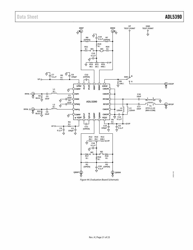
EVALUATION BOARD The evaluation board circuit schematic for the ADL5390 is shown in Figure 44.
The evaluation board is configured to be driven from a single-ended 50 Ω source. Although the input of the ADL5390 is differential, it may be driven single-ended with no loss of performance.
The low-pass corner frequency of the baseband I and Q channels can be reduced by installing capacitors in the C11 and C12 positions. The low-pass corner frequency for either channel is approximated by
pF0.5nF10kHz45
dB3 +
×≈
externalCf
On this evaluation board, the I and Q baseband circuits are identical to each other, so the following description applies to each. The connections and circuit configuration for the I/Q baseband inputs are described in Table 4.
The baseband input of the ADL5390 requires a differential voltage drive. The evaluation board is set up to allow such a drive by connecting the differential voltage source to QBBP and QBBM. The common-mode voltage should be maintained at approximately 0.5 V. For this configuration, Jumpers W1 to W4 should be removed.
The baseband input of the evaluation board may also be driven with a single-ended voltage. In this case, a bias level is provided to the unused input from Potentiometer R10 by installing either W1 or W2.
Setting SW1 in Position B disables the ADL5390 output amplifier. With SW1 set to Position A, the output amplifier is enabled. With SW1 set to Position A, an external voltage signal, such as a pulse, can be applied to the DSOP SMA connector to exercise the output amplifier enable/disable function.
ADL5390 Data Sheet
Rev. A | Page 20 of 23
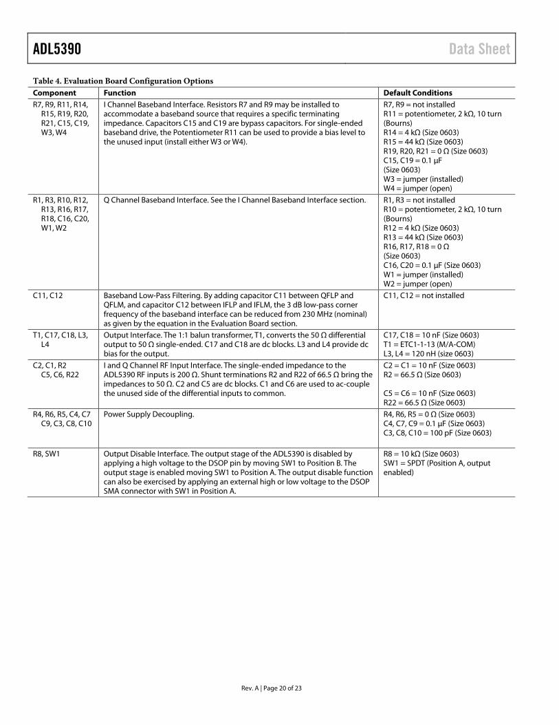
Table 4. Evaluation Board Configuration Options Component Function Default Conditions R7, R9, R11, R14,
R15, R19, R20, R21, C15, C19, W3, W4
I Channel Baseband Interface. Resistors R7 and R9 may be installed to accommodate a baseband source that requires a specific terminating impedance. Capacitors C15 and C19 are bypass capacitors. For single-ended baseband drive, the Potentiometer R11 can be used to provide a bias level to the unused input (install either W3 or W4).
R7, R9 = not installed R11 = potentiometer, 2 kΩ, 10 turn (Bourns) R14 = 4 kΩ (Size 0603) R15 = 44 kΩ (Size 0603) R19, R20, R21 = 0 Ω (Size 0603) C15, C19 = 0.1 µF (Size 0603) W3 = jumper (installed) W4 = jumper (open)
R1, R3, R10, R12, R13, R16, R17, R18, C16, C20, W1, W2
Q Channel Baseband Interface. See the I Channel Baseband Interface section. R1, R3 = not installed R10 = potentiometer, 2 kΩ, 10 turn (Bourns) R12 = 4 kΩ (Size 0603) R13 = 44 kΩ (Size 0603) R16, R17, R18 = 0 Ω (Size 0603) C16, C20 = 0.1 µF (Size 0603) W1 = jumper (installed) W2 = jumper (open)
C11, C12 Baseband Low-Pass Filtering. By adding capacitor C11 between QFLP and QFLM, and capacitor C12 between IFLP and IFLM, the 3 dB low-pass corner frequency of the baseband interface can be reduced from 230 MHz (nominal) as given by the equation in the Evaluation Board section.
C11, C12 = not installed
T1, C17, C18, L3, L4
Output Interface. The 1:1 balun transformer, T1, converts the 50 Ω differential output to 50 Ω single-ended. C17 and C18 are dc blocks. L3 and L4 provide dc bias for the output.
C17, C18 = 10 nF (Size 0603) T1 = ETC1-1-13 (M/A-COM) L3, L4 = 120 nH (size 0603)
C2, C1, R2 C5, C6, R22
I and Q Channel RF Input Interface. The single-ended impedance to the ADL5390 RF inputs is 200 Ω. Shunt terminations R2 and R22 of 66.5 Ω bring the impedances to 50 Ω. C2 and C5 are dc blocks. C1 and C6 are used to ac-couple the unused side of the differential inputs to common.
C2 = C1 = 10 nF (Size 0603) R2 = 66.5 Ω (Size 0603) C5 = C6 = 10 nF (Size 0603) R22 = 66.5 Ω (Size 0603)
R4, R6, R5, C4, C7 C9, C3, C8, C10
Power Supply Decoupling. R4, R6, R5 = 0 Ω (Size 0603) C4, C7, C9 = 0.1 µF (Size 0603) C3, C8, C10 = 100 pF (Size 0603)
R8, SW1 Output Disable Interface. The output stage of the ADL5390 is disabled by applying a high voltage to the DSOP pin by moving SW1 to Position B. The output stage is enabled moving SW1 to Position A. The output disable function can also be exercised by applying an external high or low voltage to the DSOP SMA connector with SW1 in Position A.
R8 = 10 kΩ (Size 0603) SW1 = SPDT (Position A, output enabled)
Data Sheet ADL5390
Rev. A | Page 21 of 23
0495
4-04
0
C12(OPEN)
C11(OPEN)
C8100pF
VP
C70.1F
R50
VP
R40
C3100pF
C40.1F
B
A
SW1
R810k
VPTEST POINT
GNDTEST POINT
DSOP
IBBMIBBP
VPR144k
R112k
R1544k
C150.1F
W4R210
R190
W3R200
R9(OPEN)
R7(OPEN)
C190.1F
QBBP QBBM
VP
R124k
R102k
R1344k
C160.1F
W2
R170 R16
0
W1
R180
R1(OPEN)
R3(OPEN)C20
0.1F
L20
C510nF
RFIN_QR22
66.5
L10
C210nF
RFIN_IR2
66.5C1
10nFC6
10nF
L4120nH
L3120nH
C140.1F
C10100pF
C90.1F
VP
C1710nF
C1810nF
RFOP
R60
1 5
3 4T1ETC1-1-13(M/A-COM)
IBB
P
IBB
M
VPS2
DSOP
QB
BP
QB
BM
VPRFCMRF
INMI
IPMQ
CMOP
CMOP
RFOM
RFOP
QFL
P
QFL
M
CMOP
CMOPCMRFVPRF
IFLP
IFLM
ADL5390
INPI
INPQ
Figure 44. Evaluation Board Schematic
ADL5390 Data Sheet
Rev. A | Page 22 of 23
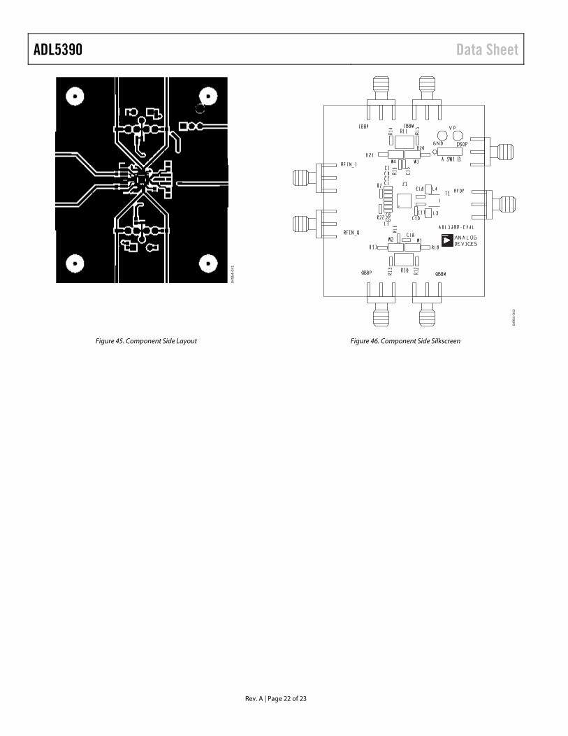
0495
4-04
1
Figure 45. Component Side Layout
0495
4-04
2
Figure 46. Component Side Silkscreen
Data Sheet ADL5390
Rev. A | Page 23 of 23
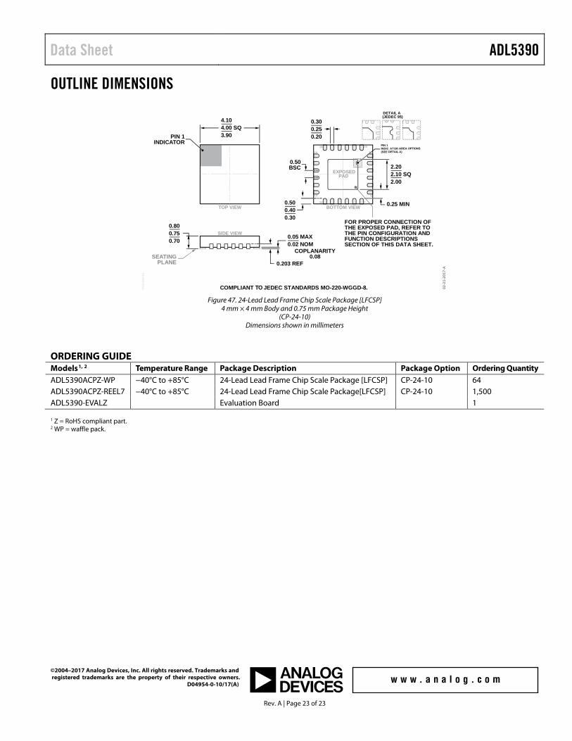
OUTLINE DIMENSIONS
0.300.250.20
0.800.750.70
0.25 MIN
2.202.10 SQ2.00
0.50BSC
0.500.400.30
COMPLIANT TO JEDEC STANDARDS MO-220-WGGD-8.
BOTTOM VIEWTOP VIEW
SIDE VIEW
4.104.00 SQ3.90
0.05 MAX0.02 NOM
0.203 REF
COPLANARITY0.08
PIN 1INDICATOR
1
24
712
13
18
19
6
FOR PROPER CONNECTION OFTHE EXPOSED PAD, REFER TOTHE PIN CONFIGURATION ANDFUNCTION DESCRIPTIONSSECTION OF THIS DATA SHEET.
02-2
1-20
17-A
EXPOSEDPAD
PKG
-004
714
SEATINGPLANE
PIN 1INDIC ATOR AREA OPTIONS(SEE DETAIL A)
DETAIL A(JEDEC 95)
Figure 47. 24-Lead Lead Frame Chip Scale Package [LFCSP]
4 mm × 4 mm Body and 0.75 mm Package Height (CP-24-10)
Dimensions shown in millimeters
ORDERING GUIDE Models1, 2 Temperature Range Package Description Package Option Ordering Quantity ADL5390ACPZ-WP −40°C to +85°C 24-Lead Lead Frame Chip Scale Package [LFCSP] CP-24-10 64 ADL5390ACPZ-REEL7 −40°C to +85°C 24-Lead Lead Frame Chip Scale Package[LFCSP] CP-24-10 1,500 ADL5390-EVALZ Evaluation Board 1 1 Z = RoHS compliant part. 2 WP = waffle pack.
©2004–2017 Analog Devices, Inc. All rights reserved. Trademarks and registered trademarks are the property of their respective owners. D04954-0-10/17(A)