Embed Size (px)
Citation preview

A2I20D020NR1 A2I20D020GNR1
1RF Device DataNXP Semiconductors
RF LDMOS Wideband IntegratedPower AmplifiersThe A2I20D020N wideband integrated circuit is designed with on--chip
matching that makes it usable from 1400 to 2200 MHz. This multi--stagestructure is rated for 20 to 32 V operation and covers all typical cellular basestation modulation formats.
1800–2200 MHz
Typical Single--Carrier W--CDMA Characterization Performance:VDD = 28 Vdc, IDQ1(A+B) = 32 mA, IDQ2(A+B) = 110 mA, Pout = 2.5 W Avg.,Input Signal PAR = 9.9 dB @ 0.01% Probability on CCDF.(1)
FrequencyGps(dB)
PAE(%)
ACPR(dBc)
1800 MHz 31.0 19.7 –44.3
1900 MHz 31.0 21.7 –45.0
2000 MHz 31.1 22.1 –45.2
2100 MHz 31.4 21.1 –45.2
2200 MHz 32.0 19.6 –44.8
1. All data measured in fixture with device soldered to heatsink.
Features
Extremely wide RF bandwidth RF decoupled drain pins reduce overall board space On--chip matching (50 ohm input, DC blocked) Integrated quiescent current temperature compensation with
enable/disable function (2)
2. Refer to AN1977, Quiescent Current Thermal Tracking Circuit in the RF Integrated Circuit Family and to AN1987,Quiescent Current Controlfor the RF Integrated Circuit Device Family. Go to http://www.nxp.com/RF. Select Documentation/Application Notes -- AN1977 or AN1987.
Document Number: A2I20D020NRev. 1, 05/2017
NXP SemiconductorsTechnical Data
1400–2200 MHz, 2.5 W AVG., 28 VAIRFAST RF LDMOS WIDEBAND
INTEGRATED POWER AMPLIFIERS
A2I20D020NR1A2I20D020GNR1
TO--270WB--17PLASTIC
A2I20D020NR1
TO--270WBG--17PLASTIC
A2I20D020GNR1
2016–2017 NXP B.V.
2RF Device Data
NXP Semiconductors
A2I20D020NR1 A2I20D020GNR1
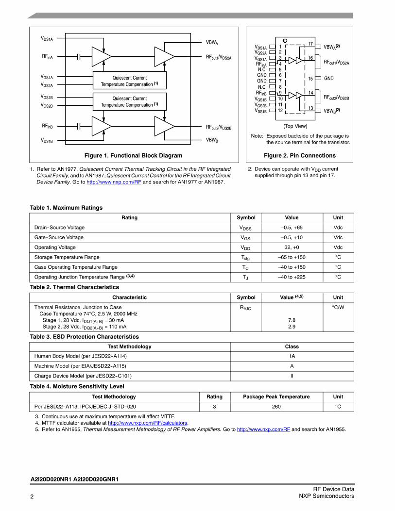
Figure 1. Functional Block Diagram Figure 2. Pin Connections
Note: Exposed backside of the package isthe source terminal for the transistor.
VDS1A
RFinA
GND
RFinB
RFout1/VDS2A
1234
78
15
VGS1B91011
VGS2AVGS1A
N.C.
N.C.
VGS2B
GND
VDS1B
RFout2/VDS2B
13
6
12
(Top View)
5
14
GND
16
17VBWA(2)
VBWB(2)
Quiescent CurrentTemperature Compensation (1)
VDS1A
RFinA
VGS1A
RFout1/VDS2A
VGS2A
Quiescent CurrentTemperature Compensation (1)
VDS1B
RFinB
VGS1B
RFout2/VDS2B
VGS2B
VBWA
VBWB
1. Refer to AN1977, Quiescent Current Thermal Tracking Circuit in the RF IntegratedCircuit Family, and to AN1987,Quiescent Current Control for theRF IntegratedCircuitDevice Family. Go to http://www.nxp.com/RF and search for AN1977 or AN1987.
2. Device can operate with VDD currentsupplied through pin 13 and pin 17.
Table 1. Maximum Ratings
Rating Symbol Value Unit
Drain--Source Voltage VDSS –0.5, +65 Vdc
Gate--Source Voltage VGS –0.5, +10 Vdc
Operating Voltage VDD 32, +0 Vdc
Storage Temperature Range Tstg –65 to +150 C
Case Operating Temperature Range TC –40 to +150 C
Operating Junction Temperature Range (3,4) TJ –40 to +225 C
Table 2. Thermal Characteristics
Characteristic Symbol Value (4,5) Unit
Thermal Resistance, Junction to CaseCase Temperature 74C, 2.5 W, 2000 MHzStage 1, 28 Vdc, IDQ1(A+B) = 30 mAStage 2, 28 Vdc, IDQ2(A+B) = 110 mA
RJC
7.82.9
C/W
Table 3. ESD Protection Characteristics
Test Methodology Class
Human Body Model (per JESD22--A114) 1A
Machine Model (per EIA/JESD22--A115) A
Charge Device Model (per JESD22--C101) II
Table 4. Moisture Sensitivity Level
Test Methodology Rating Package Peak Temperature Unit
Per JESD22--A113, IPC/JEDEC J--STD--020 3 260 C
3. Continuous use at maximum temperature will affect MTTF.4. MTTF calculator available at http://www.nxp.com/RF/calculators.5. Refer to AN1955, Thermal Measurement Methodology of RF Power Amplifiers. Go to http://www.nxp.com/RF and search for AN1955.
A2I20D020NR1 A2I20D020GNR1
3RF Device DataNXP Semiconductors
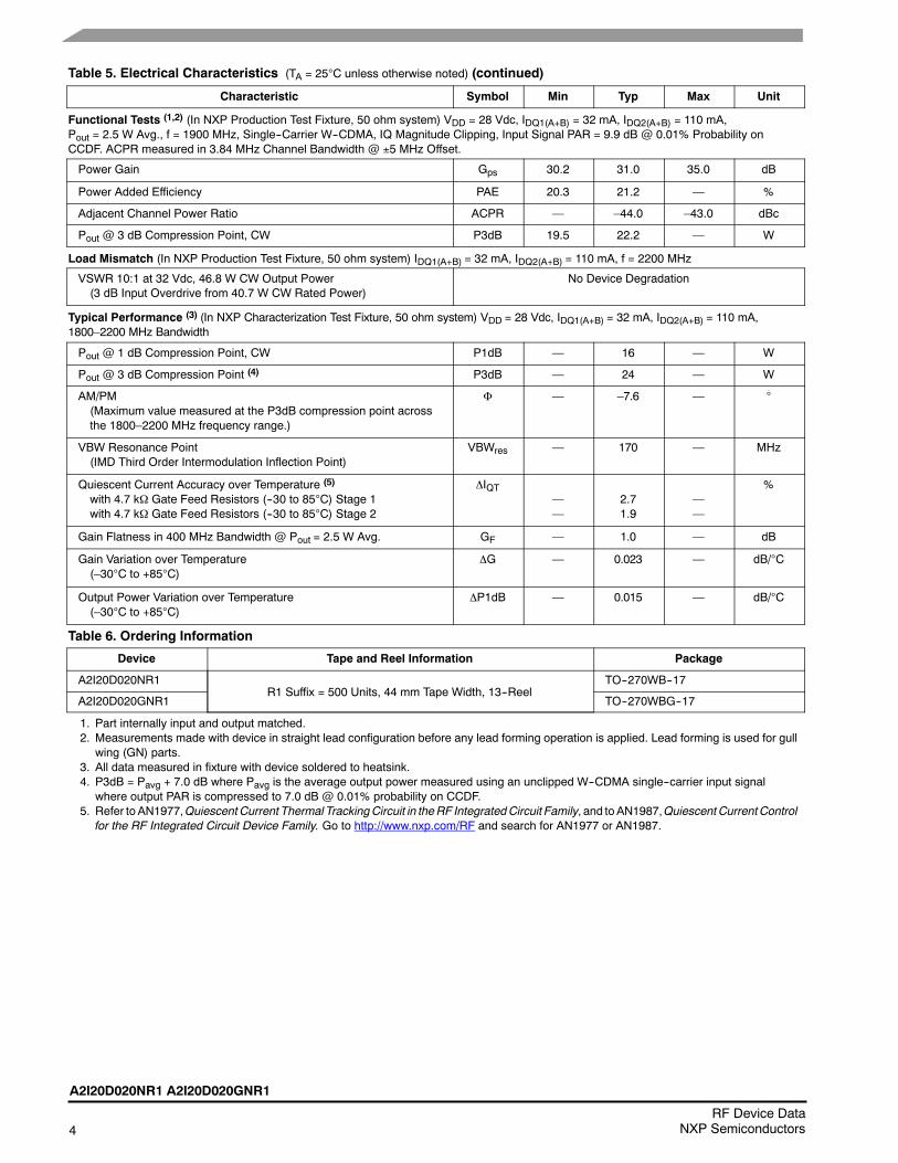
Table 5. Electrical Characteristics (TA = 25C unless otherwise noted)
Characteristic Symbol Min Typ Max Unit
Stage 1 -- Off Characteristics (1)
Zero Gate Voltage Drain Leakage Current(VDS = 65 Vdc, VGS = 0 Vdc)
IDSS — — 10 Adc
Zero Gate Voltage Drain Leakage Current(VDS = 32 Vdc, VGS = 0 Vdc)
IDSS — — 1 Adc
Gate--Source Leakage Current(VGS = 1.0 Vdc, VDS = 0 Vdc)
IGSS — — 1 Adc
Stage 1 -- On Characteristics
Gate Threshold Voltage (1)
(VDS = 10 Vdc, ID = 2 Adc)VGS(th) 0.8 1.2 1.6 Vdc
Gate Quiescent Voltage(VDS = 28 Vdc, IDQ1(A+B) = 32 mAdc)
VGS(Q) — 1.9 — Vdc
Fixture Gate Quiescent Voltage(VDD = 28 Vdc, IDQ1(A+B) = 32 mAdc, Measured in Functional Test)
VGG(Q) 7.5 8.2 9.0 Vdc
Stage 2 -- Off Characteristics (1)
Zero Gate Voltage Drain Leakage Current(VDS = 65 Vdc, VGS = 0 Vdc)
IDSS — — 10 Adc
Zero Gate Voltage Drain Leakage Current(VDS = 32 Vdc, VGS = 0 Vdc)
IDSS — — 1 Adc
Gate--Source Leakage Current(VGS = 1.0 Vdc, VDS = 0 Vdc)
IGSS — — 1 Adc
Stage 2 -- On Characteristics
Gate Threshold Voltage (1)
(VDS = 10 Vdc, ID = 11 Adc)VGS(th) 0.8 1.2 1.6 Vdc
Gate Quiescent Voltage(VDS = 28 Vdc, IDQ2(A+B) = 110 mAdc)
VGS(Q) — 1.8 — Vdc
Fixture Gate Quiescent Voltage(VDD = 28 Vdc, IDQ2(A+B) = 110 mAdc, Measured in Functional Test)
VGG(Q) 4.1 4.8 5.6 Vdc
Drain--Source On--Voltage (1)
(VGS = 10 Vdc, ID = 200 mAdc)VDS(on) 0.1 0.3 1.5 Vdc
1. Each side of device measured separately.(continued)
4RF Device Data
NXP Semiconductors
A2I20D020NR1 A2I20D020GNR1
Table 5. Electrical Characteristics (TA = 25C unless otherwise noted) (continued)
Characteristic Symbol Min Typ Max Unit
Functional Tests (1,2) (In NXP Production Test Fixture, 50 ohm system) VDD = 28 Vdc, IDQ1(A+B) = 32 mA, IDQ2(A+B) = 110 mA,Pout = 2.5 W Avg., f = 1900 MHz, Single--Carrier W--CDMA, IQ Magnitude Clipping, Input Signal PAR = 9.9 dB @ 0.01% Probability onCCDF. ACPR measured in 3.84 MHz Channel Bandwidth @ 5 MHz Offset.
Power Gain Gps 30.2 31.0 35.0 dB
Power Added Efficiency PAE 20.3 21.2 — %
Adjacent Channel Power Ratio ACPR — –44.0 –43.0 dBc
Pout @ 3 dB Compression Point, CW P3dB 19.5 22.2 — W
Load Mismatch (In NXP Production Test Fixture, 50 ohm system) IDQ1(A+B) = 32 mA, IDQ2(A+B) = 110 mA, f = 2200 MHz
VSWR 10:1 at 32 Vdc, 46.8 W CW Output Power(3 dB Input Overdrive from 40.7 W CW Rated Power)
No Device Degradation
Typical Performance (3) (In NXP Characterization Test Fixture, 50 ohm system) VDD = 28 Vdc, IDQ1(A+B) = 32 mA, IDQ2(A+B) = 110 mA,1800–2200 MHz Bandwidth
Pout @ 1 dB Compression Point, CW P1dB — 16 — W
Pout @ 3 dB Compression Point (4) P3dB — 24 — W
AM/PM(Maximum value measured at the P3dB compression point acrossthe 1800–2200 MHz frequency range.)
— –7.6 —
VBW Resonance Point(IMD Third Order Intermodulation Inflection Point)
VBWres — 170 — MHz
Quiescent Current Accuracy over Temperature (5)
with 4.7 k Gate Feed Resistors (--30 to 85C) Stage 1with 4.7 k Gate Feed Resistors (--30 to 85C) Stage 2
IQT——
2.71.9
——
%
Gain Flatness in 400 MHz Bandwidth @ Pout = 2.5 W Avg. GF — 1.0 — dB
Gain Variation over Temperature(–30C to +85C)
G — 0.023 — dB/C
Output Power Variation over Temperature(–30C to +85C)
P1dB — 0.015 — dB/C
Table 6. Ordering Information
Device Tape and Reel Information Package
A2I20D020NR1R1 Suffix = 500 Units, 44 mm Tape Width, 13--Reel
TO--270WB--17
A2I20D020GNR1 TO--270WBG--17
1. Part internally input and output matched.2. Measurements made with device in straight lead configuration before any lead forming operation is applied. Lead forming is used for gull
wing (GN) parts.3. All data measured in fixture with device soldered to heatsink.4. P3dB = Pavg + 7.0 dB where Pavg is the average output power measured using an unclipped W--CDMA single--carrier input signal
where output PAR is compressed to 7.0 dB @ 0.01% probability on CCDF.5. Refer to AN1977,Quiescent Current Thermal TrackingCircuit in theRF IntegratedCircuit Family, and to AN1987,Quiescent CurrentControl
for the RF Integrated Circuit Device Family. Go to http://www.nxp.com/RF and search for AN1977 or AN1987.
A2I20D020NR1 A2I20D020GNR1
5RF Device DataNXP Semiconductors
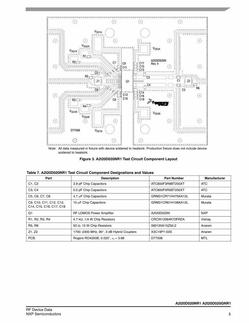
Figure 3. A2I20D020NR1 Test Circuit Component Layout
Note: All data measured in fixture with device soldered to heatsink. Production fixture does not include devicesoldered to heatsink.
A2I20D020NR1
R2
R3
R4
C5
C6
C7
C8
C11C9
C12C10
C15C13
C14C16
Z1 Z2
R5
R6
C1
C2
C3
C4
C18
C17
D77506
Rev. 4
Q1
VGG1A
VGG2AVDD2A
VDD2B
VDD1A
VGG1BVGG2B
VDD1B
Table 7. A2I20D020NR1 Test Circuit Component Designations and ValuesPart Description Part Number Manufacturer
C1, C2 3.9 pF Chip Capacitors ATC600F3R9BT250XT ATC
C3, C4 0.5 pF Chip Capacitors ATC600F0R5BT250XT ATC
C5, C6, C7, C8 4.7 F Chip Capacitors GRM31CR71H475KA12L Murata
C9, C10, C11, C12, C13,C14, C15, C16, C17, C18
10 F Chip Capacitors GRM31CR61H106KA12L Murata
Q1 RF LDMOS Power Amplifier A2I20D020N NXP
R1, R2, R3, R4 4.7 k, 1/4 W Chip Resistors CRCW12064K70FKEA Vishay
R5, R6 50 , 10 W Chip Resistors 060120A15Z50-2 Anaren
Z1, Z2 1700–2300 MHz, 90, 3 dB Hybrid Couplers X3C19P1-03S Anaren
PCB Rogers RO4350B, 0.020, r = 3.66 D77506 MTL
6RF Device Data
NXP Semiconductors
A2I20D020NR1 A2I20D020GNR1
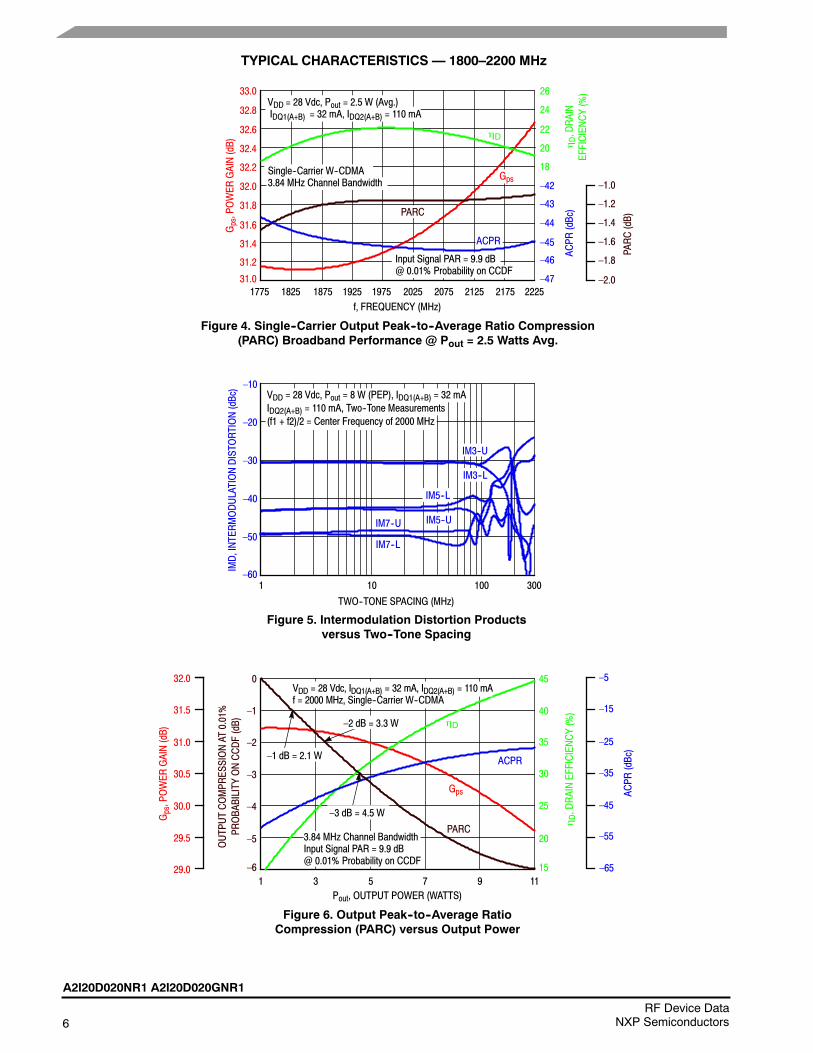
TYPICAL CHARACTERISTICS — 1800–2200 MHz
–1.8
–1.0
–1.2
–1.4
–1.6
–2.0
PARC(dB)
1775f, FREQUENCY (MHz)
Figure 4. Single--Carrier Output Peak--to--Average Ratio Compression(PARC) Broadband Performance @ Pout = 2.5 Watts Avg.
31.0
33.0
32.8
32.6
–47
26
24
22
20
–42
–43
–44
–45
D,DRAIN
EFFICIENCY(%)
Gps,POWER
GAIN(dB) 32.4
32.2
32.0
31.8
31.6
31.4
31.2
1825 1875 1925 1975 2025 2075 2125 2225
18
–46
ACPR
(dBc)
Figure 5. Intermodulation Distortion Productsversus Two--Tone Spacing
TWO--TONE SPACING (MHz)
10–60
–10
–20
–30
1 300
IMD,INTERMODULATIONDISTORTION(dBc)
Figure 6. Output Peak--to--Average RatioCompression (PARC) versus Output Power
Pout, OUTPUT POWER (WATTS)
–2
–4
3
–1
–3
–5OUTPUTCOMPRESSIONAT
0.01%
PROBABILITY
ONCCDF(dB)
1 5 715
45
40
35
30
25
20
DDRAINEFFICIENCY(%)
9
D
ACPR
PARC
ACPR
(dBc)
–65
–5
–15
–25
–45
–35
–55
32.0
Gps,POWER
GAIN(dB)
31.5
31.0
30.5
30.0
29.5
29.0
Gps
–6
0
D
IM5--U
IM7--L
IM7--U
100
IM3--U
–50
Input Signal PAR = 9.9 dB@ 0.01% Probability on CCDF
IM3--L
–40
VDD = 28 Vdc, IDQ1(A+B) = 32 mA, IDQ2(A+B) = 110 mAf = 2000 MHz, Single--Carrier W--CDMA
11
2175
VDD = 28 Vdc, Pout = 8 W (PEP), IDQ1(A+B) = 32 mAIDQ2(A+B) = 110 mA, Two--Tone Measurements(f1 + f2)/2 = Center Frequency of 2000 MHz
IM5--L
–1 dB = 2.1 W
–2 dB = 3.3 W
–3 dB = 4.5 W
VDD = 28 Vdc, Pout = 2.5 W (Avg.)IDQ1(A+B) = 32 mA, IDQ2(A+B) = 110 mA
Gps
PARC
ACPR
Single--Carrier W--CDMA3.84 MHz Channel Bandwidth
3.84 MHz Channel BandwidthInput Signal PAR = 9.9 dB@ 0.01% Probability on CCDF
A2I20D020NR1 A2I20D020GNR1
7RF Device DataNXP Semiconductors
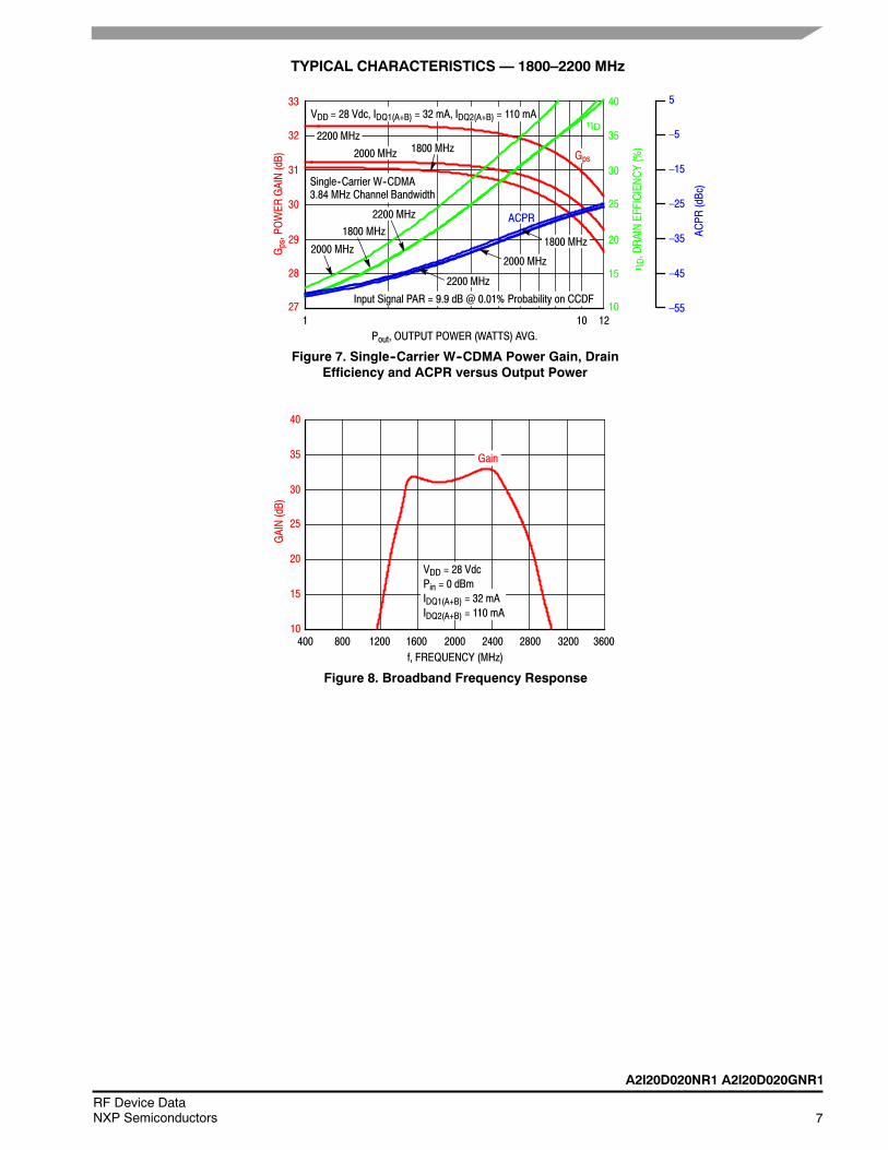
TYPICAL CHARACTERISTICS — 1800–2200 MHz
1Pout, OUTPUT POWER (WATTS) AVG.
Figure 7. Single--Carrier W--CDMA Power Gain, DrainEfficiency and ACPR versus Output Power
–15
27
33
10
40
35
30
25
20
D,DRAINEFFICIENCY(%)
Gps,POWER
GAIN(dB)
32
31
10 12
15
–55
ACPR
(dBc)
30
29
28
5
–25
–35
–45
ACPR
D
Figure 8. Broadband Frequency Response
10
40
f, FREQUENCY (MHz)
30
25
20
GAIN(dB)
35
15
400 800 1200 1600 2000 2400 2800 3200 3600
Gain
Input Signal PAR = 9.9 dB @ 0.01% Probability on CCDF
VDD = 28 Vdc, IDQ1(A+B) = 32 mA, IDQ2(A+B) = 110 mA
Single--Carrier W--CDMA3.84 MHz Channel Bandwidth
1800 MHz2000 MHz
2200 MHz
2000 MHz
1800 MHz
2200 MHz
–5
2000 MHz
2200 MHz
VDD = 28 VdcPin = 0 dBmIDQ1(A+B) = 32 mAIDQ2(A+B) = 110 mA
Gps
1800 MHz

8RF Device Data
NXP Semiconductors
A2I20D020NR1 A2I20D020GNR1
Table 8. Load Pull Performance — Maximum Power TuningVDD = 28 Vdc, IDQ1 = 16 mA, IDQ2 = 57 mA, Pulsed CW, 10 sec(on), 10% Duty Cycle
f(MHz)
Zsource()
Zin()
Max Output Power
P1dB
Zload (1)
() Gain (dB) (dBm) (W)D(%)
AM/PM()
1805 92.7 + j84.9 72.9 – j80.3 21.8 – j4.48 31.6 40.6 11 54.5 –3
1840 70.5 + j83.3 62.6 – j79.4 19.0 – j6.17 31.4 40.6 11 52.5 –3
1880 53.3 + j79.4 50.7 – j74.5 17.9 – j5.52 31.3 40.6 12 51.6 –3
f(MHz)
Zsource()
Zin()
Max Output Power
P3dB
Zload (2)
() Gain (dB) (dBm) (W)D(%)
AM/PM()
1805 92.7 + j84.9 71.2 – j79.5 20.1 – j7.48 29.3 41.5 14 53.7 –6
1840 70.5 + j83.3 61.5 – j78.8 18.5 – j6.91 29.3 41.5 14 52.8 –6
1880 53.3 + j79.4 50.1 – j73.8 17.5 – j6.54 29.2 41.5 14 51.8 –5
(1) Load impedance for optimum P1dB power.(2) Load impedance for optimum P3dB power.Zsource = Measured impedance presented to the input of the device at the package reference plane.Zin = Impedance as measured from gate contact to ground.Zload = Measured impedance presented to the output of the device at the package reference plane.
Note: Measurement made on a per side basis.
Table 9. Load Pull Performance — Maximum Efficiency TuningVDD = 28 Vdc, IDQ1 = 16 mA, IDQ2 = 57 mA, Pulsed CW, 10 sec(on), 10% Duty Cycle
f(MHz)
Zsource()
Zin()
Max Drain Efficiency
P1dB
Zload (1)
() Gain (dB) (dBm) (W)D(%)
AM/PM()
1805 92.7 + j84.9 73.1 – j84.4 41.8 + j7.22 32.9 39.0 8 61.7 –5
1840 70.5 + j83.3 62.4 – j82.2 32.6 + j4.15 32.6 39.4 9 59.9 –4
1880 53.3 + j79.4 50.5 – j77.9 26.6 + j12.0 33.0 38.8 8 57.5 –5
f(MHz)
Zsource()
Zin()
Max Drain Efficiency
P3dB
Zload (2)
() Gain (dB) (dBm) (W)D(%)
AM/PM()
1805 92.7 + j84.9 72.6 – j82.9 41.0 + j3.98 30.8 40.0 10 61.1 –8
1840 70.5 + j83.3 62.5 – j81.6 30.9 + j5.87 30.6 40.3 11 59.8 –7
1880 53.3 + j79.4 50.2 – j76.9 30.1 + j10.2 30.9 39.7 9 58.1 –6
(1) Load impedance for optimum P1dB efficiency.(2) Load impedance for optimum P3dB efficiency.Zsource = Measured impedance presented to the input of the device at the package reference plane.Zin = Impedance as measured from gate contact to ground.Zload = Measured impedance presented to the output of the device at the package reference plane.
Note: Measurement made on a per side basis.
Input Load PullTuner and TestCircuit
DeviceUnderTest
Zsource Zin Zload
Output Load PullTuner and TestCircuit
A2I20D020NR1 A2I20D020GNR1
9RF Device DataNXP Semiconductors
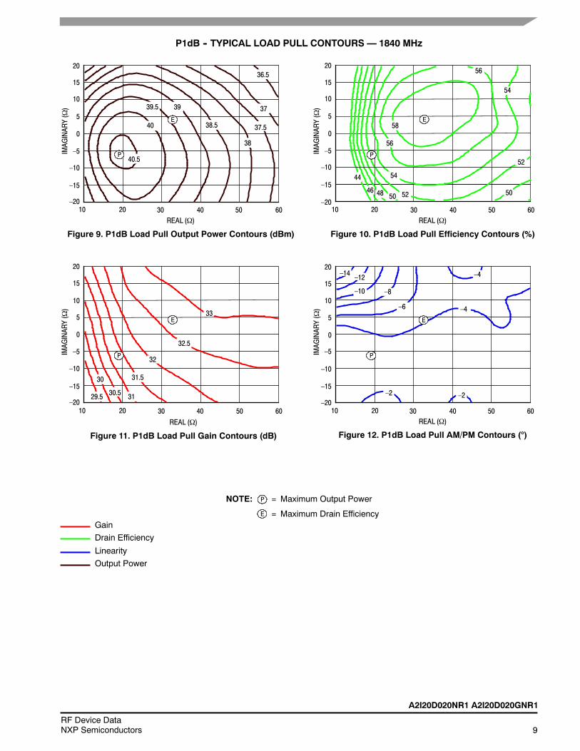
P1dB -- TYPICAL LOAD PULL CONTOURS — 1840 MHz
IMAGINARY()
IMAGINARY()
IMAGINARY()
IMAGINARY()
NOTE: = Maximum Output Power
= Maximum Drain Efficiency
P
E
Gain
Drain Efficiency
Linearity
Output Power
Figure 9. P1dB Load Pull Output Power Contours (dBm)
REAL ()
Figure 10. P1dB Load Pull Efficiency Contours (%)
REAL ()
Figure 11. P1dB Load Pull Gain Contours (dB)
REAL ()
Figure 12. P1dB Load Pull AM/PM Contours ()
REAL ()
P
E
30.5
30
29.5
32
32.5
31
31.5
33
P
–14
39.5
40 37.5
39
40.5
38.5
37
38
58
54
56
52 50
–12
–10 –8
–6 –4
–2
P
E
E
P
E
20
15
10
5
0
–20
–15
–10
–5
20
15
10
5
0
–20
–15
–10
–5
20 30 40 6010 50 20 30 40 6010 50
20 30 40 6010 50 20 30 40 6010 50
20
15
10
5
0
–20
–15
–10
–5
20
15
10
5
0
–20
–15
–10
–5
36.5
52
54
5048
44
46
56
–4
–2
10RF Device Data
NXP Semiconductors
A2I20D020NR1 A2I20D020GNR1
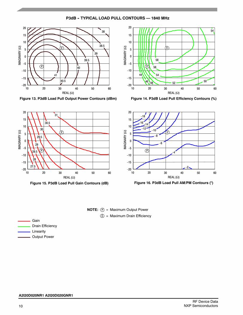
P3dB -- TYPICAL LOAD PULL CONTOURS — 1840 MHz
NOTE: = Maximum Output Power
= Maximum Drain Efficiency
P
E
Gain
Drain Efficiency
Linearity
Output Power
20
15
IMAGINARY()
20 30 40 6010
Figure 13. P3dB Load Pull Output Power Contours (dBm)
REAL ()
39.5
40
39
40.5
38.5
41
38
IMAGINARY()
Figure 14. P3dB Load Pull Efficiency Contours (%)
REAL ()
58
54
56
IMAGINARY()
Figure 15. P3dB Load Pull Gain Contours (dB)
REAL ()
28.5
29.5
30
29
IMAGINARY()
Figure 16. P3dB Load Pull AM/PM Contours ()
REAL ()
10
5
0
–2052 50
27.5
28
30.5
31
–14–12 –10
–8
–6
–4
–2
–18
–16
P
E
P
E
P
E
P
E
–15
–10
–5
50
20
15
10
5
0
–20
–15
–10
–5
20 30 40 6010 50
20
15
10
5
0
–20
–15
–10
–5
20
15
10
5
0
–20
–15
–10
–5
20 30 40 6010 50 20 30 40 6010 50
48
44
46
54
A2I20D020NR1 A2I20D020GNR1
11RF Device DataNXP Semiconductors
Table 10. Load Pull Performance — Maximum Power TuningVDD = 28 Vdc, IDQ1 = 16 mA, IDQ2 = 57 mA, Pulsed CW, 10 sec(on), 10% Duty Cycle
f(MHz)
Zsource()
Zin()
Max Output Power
P1dB
Zload (1)
() Gain (dB) (dBm) (W)D(%)
AM/PM()
2110 26.5 + j66.6 26.8 – j66.8 17.2 + j0.65 32.6 40.6 12 50.7 –4
2140 28.6 + j67.5 26.6 – j69.1 18.0 + j1.74 33.3 40.7 12 52.9 –5
2170 27.7 + j71.6 28.6 – j71.2 16.6 + j2.92 33.9 40.8 12 55.3 –5
f(MHz)
Zsource()
Zin()
Max Output Power
P3dB
Zload (2)
() Gain (dB) (dBm) (W)D(%)
AM/PM()
2110 26.5 + j66.6 26.3 – j66.3 17.2 + j0.31 30.6 41.5 14 52.3 –7
2140 28.6 + j67.5 26.1 – j68.6 17.4 + j1.43 31.3 41.6 14 53.6 –8
2170 27.7 + j71.6 28.0 – j70.2 18.6 + j0.54 31.5 41.7 15 54.5 –9
(1) Load impedance for optimum P1dB power.(2) Load impedance for optimum P3dB power.Zsource = Measured impedance presented to the input of the device at the package reference plane.Zin = Impedance as measured from gate contact to ground.Zload = Measured impedance presented to the output of the device at the package reference plane.
Note: Measurement made on a per side basis.
Table 11. Load Pull Performance — Maximum Efficiency TuningVDD = 28 Vdc, IDQ1 = 16 mA, IDQ2 = 57 mA, Pulsed CW, 10 sec(on), 10% Duty Cycle
f(MHz)
Zsource()
Zin()
Max Drain Efficiency
P1dB
Zload (1)
() Gain (dB) (dBm) (W)D(%)
AM/PM()
2110 26.5 + j66.6 26.0 – j67.4 15.9 + j12.4 34.1 39.4 9 58.3 –5
2140 28.6 + j67.5 26.1 – j69.4 16.2 + j12.9 34.6 39.7 9 60.9 –6
2170 27.7 + j71.6 28.1 – j71.5 13.7 + j12.4 35.1 39.6 9 64.3 –8
f(MHz)
Zsource()
Zin()
Max Drain Efficiency
P3dB
Zload (2)
() Gain (dB) (dBm) (W)D(%)
AM/PM()
2110 26.5 + j66.6 25.7 – j67.3 16.2 + j12.1 32.0 40.5 11 60.0 –7
2140 28.6 + j67.5 25.6 – j69.4 14.7 + j12.9 32.7 40.4 11 61.8 –9
2170 27.7 + j71.6 27.4 – j71.4 14.2 + j13.7 33.2 40.2 10 63.5 –11
(1) Load impedance for optimum P1dB efficiency.(2) Load impedance for optimum P3dB efficiency.Zsource = Measured impedance presented to the input of the device at the package reference plane.Zin = Impedance as measured from gate contact to ground.Zload = Measured impedance presented to the output of the device at the package reference plane.
Note: Measurement made on a per side basis.
Input Load PullTuner and TestCircuit
DeviceUnderTest
Zsource Zin Zload
Output Load PullTuner and TestCircuit

12RF Device Data
NXP Semiconductors
A2I20D020NR1 A2I20D020GNR1
P1dB -- TYPICAL LOAD PULL CONTOURS — 2140 MHz
NOTE: = Maximum Output Power
= Maximum Drain Efficiency
P
E
Gain
Drain Efficiency
Linearity
Output Power
IMAGINARY()
20 30 40 5010
Figure 17. P1dB Load Pull Output Power Contours (dBm)
REAL ()
Figure 18. P1dB Load Pull Efficiency Contours (%)
REAL ()
IMAGINARY()
IMAGINARY()
Figure 19. P1dB Load Pull Gain Contours (dB)
REAL ()
IMAGINARY()
Figure 20. P1dB Load Pull AM/PM Contours ()
REAL ()
6039.540
39
40.558
46
48
54
56
5250
44
32
32.5
31.5
33
34
34.5
33.5
35
–8
–6 –4
–2
P
E E
P
E
P P
E
20
15
10
5
0
–10
–5
20 30 40 5010
20 30 4010 50
20
15
10
5
0
–10
–5
20 30 40 5010
20
15
10
5
0
–10
–5
20
15
10
5
0
–10
–5
40
39.539
–4

A2I20D020NR1 A2I20D020GNR1
13RF Device DataNXP Semiconductors
P3dB -- TYPICAL LOAD PULL CONTOURS — 2140 MHz
NOTE: = Maximum Output Power
= Maximum Drain Efficiency
P
E
Gain
Drain Efficiency
Linearity
Output Power
IMAGINARY()
20 30 40 5010
Figure 21. P3dB Load Pull Output Power Contours (dBm)
REAL ()
Figure 22. P3dB Load Pull Efficiency Contours (%)
REAL ()
IMAGINARY()
58
60
46
50525456
IMAGINARY()
Figure 23. P3dB Load Pull Gain Contours (dB)
REAL ()
IMAGINARY()
Figure 24. P3dB Load Pull AM/PM Contours ()
REAL ()
48
39.540
41.5
40.5
41
32.5
29.5 30
31.5
33
30.5
31
–12
–8 –6
–4
–2
–10
P
E
P
E
P
E
P
E
20
15
10
5
0
–10
–5
20
15
10
5
0
–10
–5
20 30 40 5010
20
15
10
5
0
–10
–5
20 30 40 5010 20 30 40 5010
20
15
10
5
0
–10
–5
39
32
–8
14RF Device Data
NXP Semiconductors
A2I20D020NR1 A2I20D020GNR1
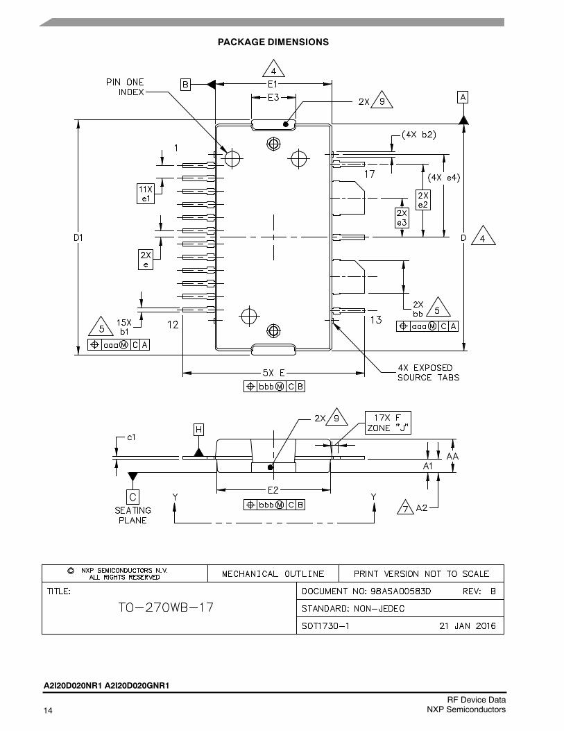
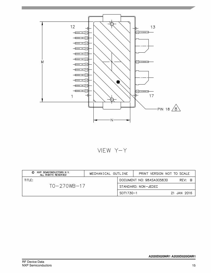
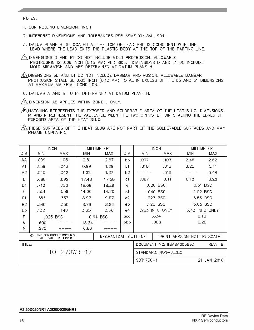
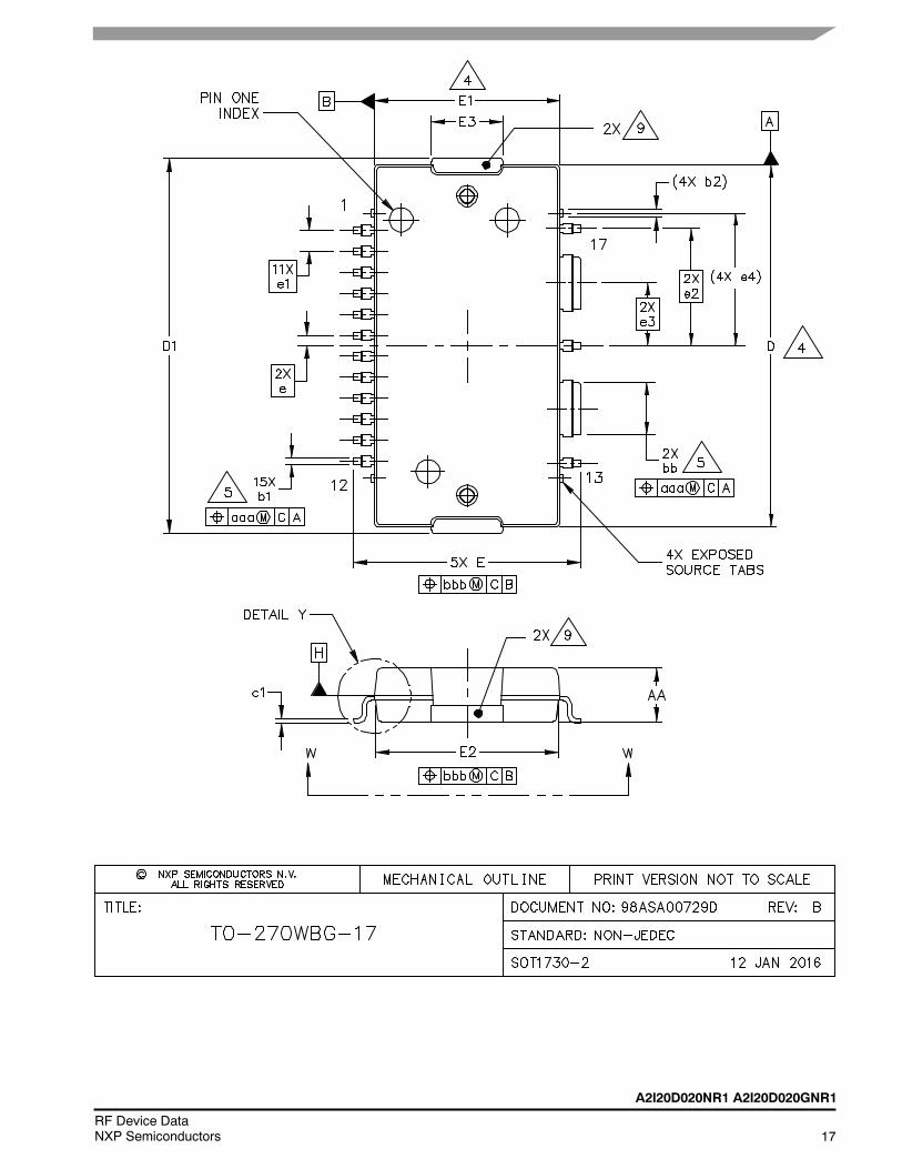
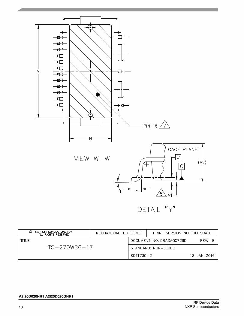
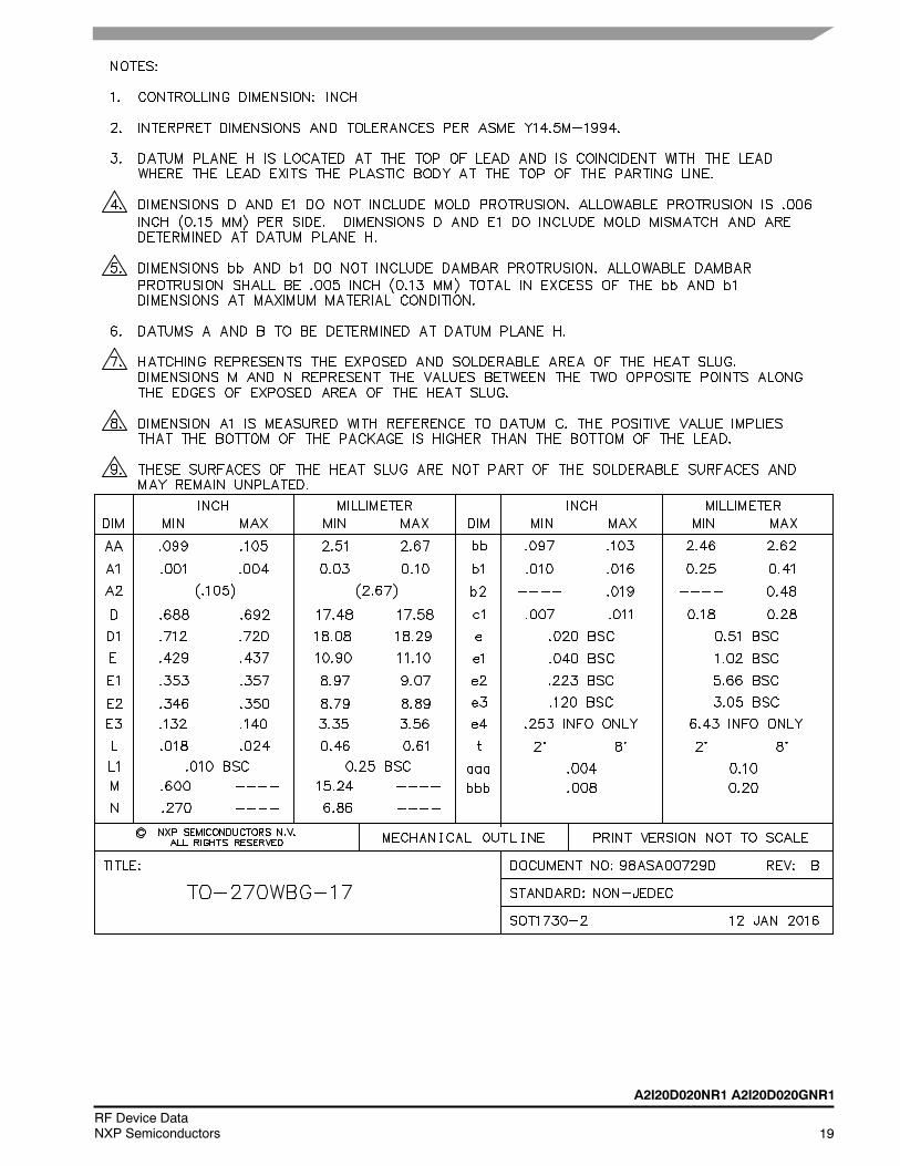
PACKAGE DIMENSIONS
A2I20D020NR1 A2I20D020GNR1
15RF Device DataNXP Semiconductors
16RF Device Data
NXP Semiconductors
A2I20D020NR1 A2I20D020GNR1
A2I20D020NR1 A2I20D020GNR1
17RF Device DataNXP Semiconductors
18RF Device Data
NXP Semiconductors
A2I20D020NR1 A2I20D020GNR1
A2I20D020NR1 A2I20D020GNR1
19RF Device DataNXP Semiconductors
20RF Device Data
NXP Semiconductors
A2I20D020NR1 A2I20D020GNR1
PRODUCT DOCUMENTATION, SOFTWARE AND TOOLS
Refer to the following resources to aid your design process.
Application Notes AN1907: Solder Reflow Attach Method for High Power RF Devices in Over--Molded Plastic Packages
AN1955: Thermal Measurement Methodology of RF Power Amplifiers
AN1977: Quiescent Current Thermal Tracking Circuit in the RF Integrated Circuit Family
AN1987: Quiescent Current Control for the RF Integrated Circuit Device Family
Engineering Bulletins EB212: Using Data Sheet Impedances for RF LDMOS Devices
Software Electromigration MTTF Calculator
RF High Power Model
.s2p File
Development Tools Printed Circuit Boards
To Download Resources Specific to a Given Part Number:1. Go to http://www.nxp.com/RF
2. Search by part number
3. Click part number link
4. Choose the desired resource from the drop down menu
REVISION HISTORY
The following table summarizes revisions to this document.
Revision Date Description
0 May 2016 Initial release of data sheet
1 May 2017 Typical Performance table: added VBWres, p. 4
1800–2200 MHz characterization fixture: added typical characteristic performance graphs, pp. 6--7

A2I20D020NR1 A2I20D020GNR1
21RF Device DataNXP Semiconductors
How to Reach Us:
Home Page:nxp.com
Web Support:nxp.com/support
Information in this document is provided solely to enable system and softwareimplementers to use NXP products. There are no express or implied copyright licensesgranted hereunder to design or fabricate any integrated circuits based on the informationin this document. NXP reserves the right to make changes without further notice to anyproducts herein.
NXP makes no warranty, representation, or guarantee regarding the suitability of itsproducts for any particular purpose, nor does NXP assume any liability arising out of theapplication or use of any product or circuit, and specifically disclaims any and all liability,including without limitation consequential or incidental damages. “Typical” parametersthat may be provided in NXP data sheets and/or specifications can and do vary indifferent applications, and actual performance may vary over time. All operatingparameters, including “typicals,” must be validated for each customer application bycustomer’s technical experts. NXP does not convey any license under its patent rightsnor the rights of others. NXP sells products pursuant to standard terms and conditions ofsale, which can be found at the following address: nxp.com/SalesTermsandConditions.
NXP, the NXP logo, Freescale, the Freescale logo, and Airfast are trademarks ofNXP B.V. All other product or service names are the property of their respective owners.E 2016–2017 NXP B.V.
Document Number: A2I20D020NRev. 1, 05/2017