Embed Size (px)
Citation preview
Utility mSATA 401-0452-00 Rev. B
© 2019 | Delkin Devices Inc.
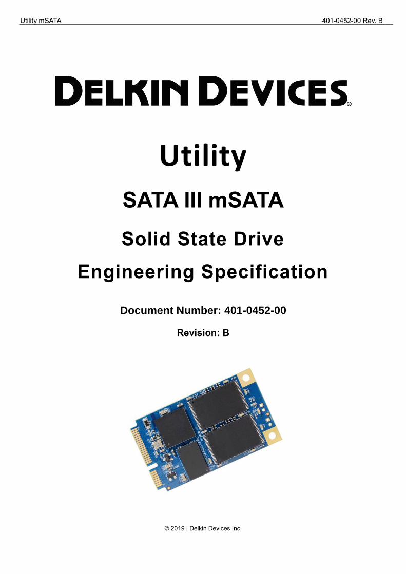
Utility
SATA III mSATA
Solid State Drive
Engineering Specification
Document Number: 401-0452-00
Revision: B
Utility mSATA 401-0452-00 Rev. B
© 2019 | Delkin Devices Inc. 2
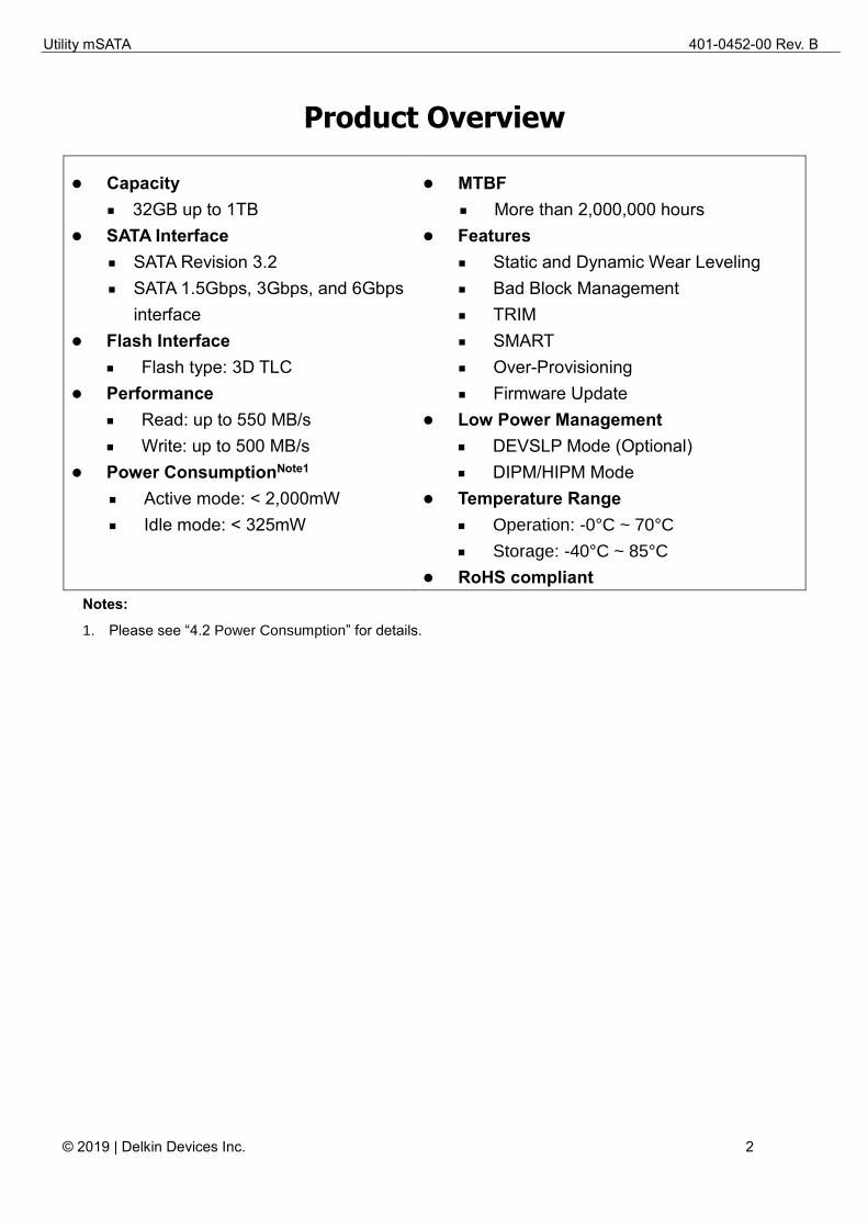
Product Overview
⚫ Capacity
■ 32GB up to 1TB
⚫ SATA Interface
■ SATA Revision 3.2
■ SATA 1.5Gbps, 3Gbps, and 6Gbps
interface
⚫ Flash Interface
■ Flash type: 3D TLC
⚫ Performance
■ Read: up to 550 MB/s
■ Write: up to 500 MB/s
⚫ Power ConsumptionNote1
■ Active mode: < 2,000mW
■ Idle mode: < 325mW
⚫ MTBF
■ More than 2,000,000 hours
⚫ Features
■ Static and Dynamic Wear Leveling
■ Bad Block Management
■ TRIM
■ SMART
■ Over-Provisioning
■ Firmware Update
⚫ Low Power Management
■ DEVSLP Mode (Optional)
■ DIPM/HIPM Mode
⚫ Temperature Range
■ Operation: -0°C ~ 70°C
■ Storage: -40°C ~ 85°C
⚫ RoHS compliant
Notes:
1. Please see “4.2 Power Consumption” for details.
Utility mSATA 401-0452-00 Rev. B
© 2019 | Delkin Devices Inc. 3
TABLE OF CONTENTS
UTILITY ...................................................................................................................................... 1
SOLID STATE DRIVE .................................................................................................................... 1
ENGINEERING SPECIFICATION..................................................................................................... 1
1. INTRODUCTION........................................................................................................... 5
1.1. General Description ........................................................................................................ 5
1.2. Product Block Diagram .................................................................................................. 5
1.3. Flash Management ......................................................................................................... 5
1.3.1. Error Correction Code (ECC) ............................................................................. 5
1.3.2. Wear Leveling ....................................................................................................... 5
1.3.3. Bad Block Management ...................................................................................... 6
1.3.4. TRIM ....................................................................................................................... 6
1.3.5. SMART .................................................................................................................. 6
1.3.6. Over-Provisioning ................................................................................................. 6
1.3.7. Firmware Upgrades ............................................................................................. 7
1.4. Low Power Management ............................................................................................... 7
1.4.1. DEVSLP Mode (Optional) ................................................................................... 7
1.4.2. DIPM/HIPM Mode ................................................................................................ 7
1.5. Power Loss Protection: Flushing Mechanism ............................................................ 7
1.6. Advanced Device Security Features ............................................................................ 8
1.6.1. Secure Erase ........................................................................................................ 8
1.6.2. Write Protect ......................................................................................................... 8
1.7. SSD Lifetime Management............................................................................................ 8
1.7.1. Thermal Monitor (Optional)................................................................................. 8
1.8. An Adaptive Approach to Performance Tuning .......................................................... 8
1.8.1. Throughput ............................................................................................................ 8
1.8.2. Predict & Fetch ..................................................................................................... 9
2. PRODUCT SPECIFICATIONS................................................................................... 10
3. ENVIRONMENTAL SPECIFICATIONS..................................................................... 12
3.1. Environmental Conditions ............................................................................................ 12
3.1.1. Temperature and Humidity ............................................................................... 12
3.1.2. Shock & Vibration ............................................................................................... 12
3.1.3. Electrostatic Discharge (ESD) ......................................................................... 12
3.1.4. EMI Compliance ................................................................................................. 12
3.2. MTBF .............................................................................................................................. 12
Utility mSATA 401-0452-00 Rev. B
© 2019 | Delkin Devices Inc. 4
3.3. Certification & Compliance .......................................................................................... 13
4. ELECTRICAL SPECIFICATIONS ............................................................................. 14
4.1. Supply Voltage ............................................................................................................... 14
4.2. Power Consumption ..................................................................................................... 14
5. INTERFACE ................................................................................................................ 15
5.1. Pin Assignment and Descriptions ............................................................................... 15
6. SUPPORTED COMMANDS ....................................................................................... 17
6.1. ATA Command List ....................................................................................................... 17
6.2. Identify Device Data...................................................................................................... 19
7. PHYSICAL DIMENSIONS .......................................................................................... 23
LIST OF FIGURES
Figure 1-2 mSATA SSD Product Block Diagram ............................................. 5
LIST OF TABLES
Table 4-1 Supply Voltage ................................................................................... 14
Table 4-2 Power Consumption ......................................................................... 14
Table 5-1 Pin Assignment and Description for mSATA .................................. 15
Table 6-1 ATA Command List ............................................................................ 17
Table 6-2 List of Device Identification .............................................................. 19
Table 6-3 List of Device Identification for Each Capacity ............................... 22
Utility mSATA 401-0452-00 Rev. B
© 2019 | Delkin Devices Inc. 5
1. INTRODUCTION
1.1. General Description
Delkin’s Utility mSATA Solid State Drive (SSD) delivers all the advantages of flash disk technology
with Serial ATA I/II/III interface and is fully compliant with the JEDEC MO-300B form factor standard.
The mSATA draws significantly lower power compared to traditional hard drives. The drive is
available in capacities from 32GB to 1TB and can reach speeds up to 550MB/s read as well as
500MB/s write (measured by CrystalDiskMark v5.0).
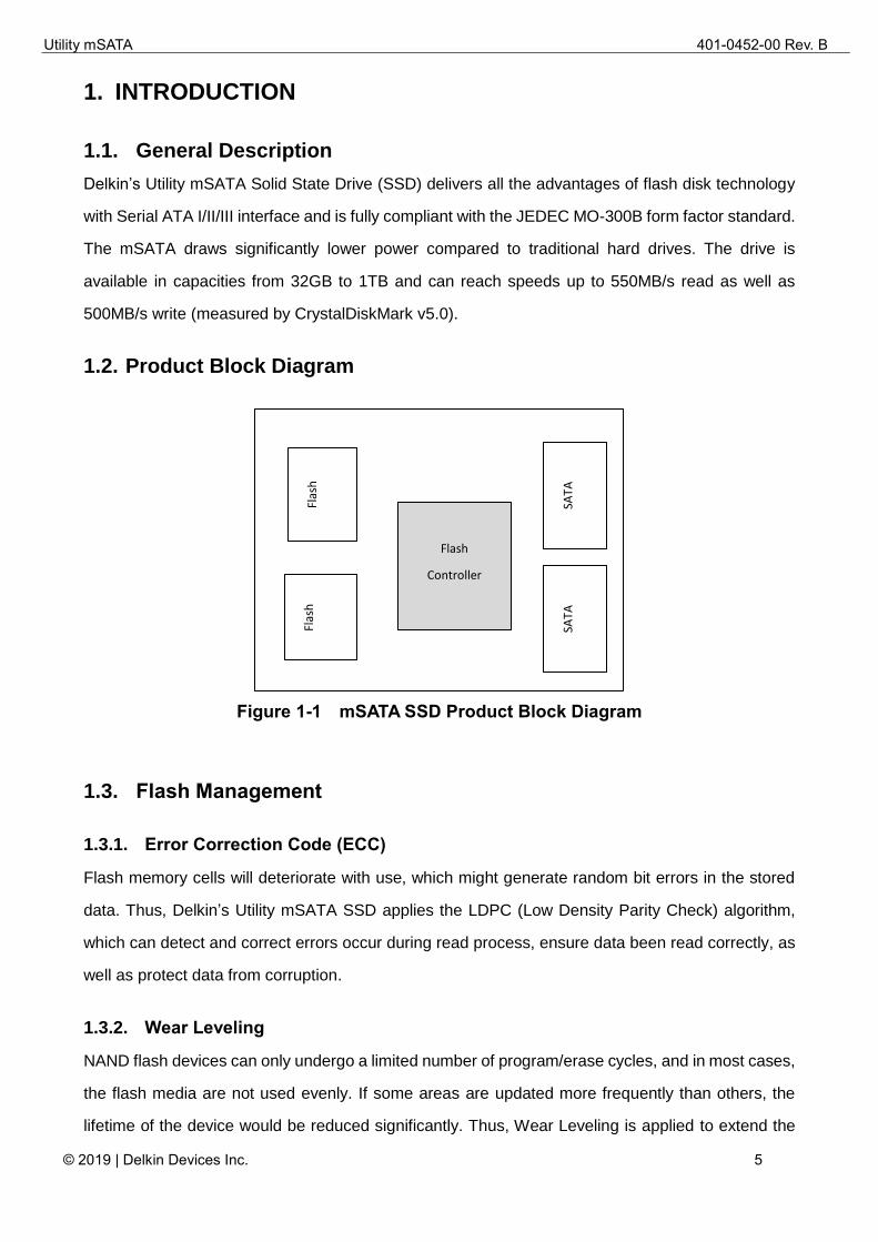
1.2. Product Block Diagram
Figure 1-1 mSATA SSD Product Block Diagram
1.3. Flash Management
1.3.1. Error Correction Code (ECC)
Flash memory cells will deteriorate with use, which might generate random bit errors in the stored
data. Thus, Delkin’s Utility mSATA SSD applies the LDPC (Low Density Parity Check) algorithm,
which can detect and correct errors occur during read process, ensure data been read correctly, as
well as protect data from corruption.
1.3.2. Wear Leveling
NAND flash devices can only undergo a limited number of program/erase cycles, and in most cases,
the flash media are not used evenly. If some areas are updated more frequently than others, the
lifetime of the device would be reduced significantly. Thus, Wear Leveling is applied to extend the
Flas
h
Flash
Controller SA
TA
SATA
Flas
h
Utility mSATA 401-0452-00 Rev. B
© 2019 | Delkin Devices Inc. 6
lifespan of NAND flash by evenly distributing write and erase cycles across the media.
Delkin utilizes advanced Wear Leveling algorithms, which can efficiently distribute flash usage
through the whole flash media area. Moreover, by implementing both dynamic and static Wear
Leveling algorithms, the life expectancy of the NAND flash is greatly improved.
1.3.3. Bad Block Management
Bad blocks are blocks that include one or more invalid bits, and their reliability is not guaranteed.
Blocks that are identified and marked as bad by the manufacturer are referred to as “Initial Bad
Blocks”. Bad blocks that are developed during usage of the flash are named “Later Bad Blocks”.
Delkin implements an efficient bad block management algorithm to detect the factory-produced bad
blocks and manages any bad blocks that appear with use. This practice further prevents data being
stored into bad blocks and improves data reliability.
1.3.4. TRIM
TRIM is a feature which helps improve the read/write performance and speed of solid-state drives
(SSD). Unlike hard disk drives (HDD), SSDs are not able to overwrite existing data, so the available
space gradually becomes smaller with each use. With the TRIM command, the operating system
can inform the SSD which blocks of data are no longer in use and can be removed permanently.
Thus, the SSD will perform an erase action, which prevents unused data from occupying blocks.
1.3.5. SMART
SMART, an acronym for Self-Monitoring, Analysis and Reporting Technology, is an open standard
that allows a drive to automatically detect its health and report potential failures. When a failure is
recorded by SMART, users can choose to replace the drive to prevent unexpected outage or data
loss. Moreover, SMART can inform users of impending failures while there is still time to perform
proactive actions, such as copy data to another device.
1.3.6. Over-Provisioning
Over Provisioning refers to the inclusion of extra NAND capacity in a SSD, which is not visible or
usable by users. With Over Provisioning, the performance and IOPS (Input/Output Operations per
Second) are improved by providing the controller additional space to manage P/E cycles, which
enhances the reliability and endurance as well. Moreover, the write amplification of the SSD
becomes lower when the controller writes data to the flash.
Utility mSATA 401-0452-00 Rev. B
© 2019 | Delkin Devices Inc. 7
1.3.7. Firmware Upgrades
Firmware can be considered as a set of instructions on how the device communicates with the host.
Firmware can be upgraded when new features are added, compatibility issues are fixed, or
read/write performance gets improved, as controlled by the user.
1.4. Low Power Management
1.4.1. DEVSLP Mode (Optional)
With the increasing need of aggressive power/battery life, SATA interfaces include a new feature,
Device Sleep (DEVSLP) mode, which helps further reduce the power consumption of the device.
DEVSLP enables the device to completely power down the device PHY and other sub-systems,
making the device reach a new level of lower power operation. The DEVSLP does not specify the
exact power level a device can achieve in the DEVSLP mode, but the power usage can be dropped
down to 5mW or less.
1.4.2. DIPM/HIPM Mode
SATA interfaces contain two low power management states for power saving: Partial and Slumber
modes. In Partial mode, the device must resume full operation within 10 microseconds, whereas in
Slumber mode, the device has 10 milliseconds to become fully operational. SATA interfaces allow
low power modes to be initiated by Host (HIPM, Host Initiated Power Management) or Device (DIPM,
Device Initiated Power Management). As for HIPM, Partial or Slumber mode can be invoked directly
by the software. For DIPM, the device will send requests to enter Partial or Slumber mode.
1.5. Power Loss Protection: Flushing Mechanism
Power Loss Protection is a mechanism to prevent data loss during unexpected power failures. DRAM
is volatile memory and frequently used as temporary cache or buffer between the controller and the
NAND flash to improve SSD performance. However, one major concern of the DRAM is that data
could be lost in the event of a power failure. Accordingly, the Delkin SATA controller applies the
GuaranteedFlush technology, which requests the controller to transfer data to the cache. Only when
the data is fully committed to the NAND flash will the controller send acknowledgement (ACK) to the
host. Such implementation can prevent false-positive performance and the risk of power cycling
issues.
Additionally, it is critical for a controller to shorten the time the in-flight data stays in the cache. Thus,
Delkin’s controller applies an algorithm to reduce the amount of data residing in the cache to provide
Utility mSATA 401-0452-00 Rev. B
© 2019 | Delkin Devices Inc. 8
better performance. This SmartCacheFlush technology allows incoming data to have only a brief
“pit stop” in the cache and then move straight to the NAND flash. If the flash is jammed due to
particular file sizes (such as random 4KB data), the cache will be treated as an “organizer”,
consolidating incoming data into groups before written into the flash to improve write amplification.
In summary, with this advanced Flush Mechanism, Delkin’s controller provides the reliability and
data protection required by today’s applications and hosts.
1.6. Advanced Device Security Features
1.6.1. Secure Erase
Secure Erase is a standard ATA command and will write “0xFF” to all cells, to fully wipe all the data
on hard drives and SSDs. When this command is issued, the SSD controller will erase its storage
blocks and return to its factory default settings.
1.6.2. Write Protect
When a SSD contains too many bad blocks and data is continuously written in, then the SSD may
no longer be usable. Thus, Write Protect is a mechanism to prevent data from being written in and
protect the accuracy of data that are already stored in the SSD.
1.7. SSD Lifetime Management
1.7.1. Thermal Monitor (Optional)
Thermal monitors are devices for measuring temperature, and can be found in SSDs in order to
issue warnings when SSDs go beyond a certain temperature. The higher the temperature the
thermal monitor detects, the more power the SSD consumes, causing the SSD to age quickly.
Therefore, the processing speed of the SSD will be under control to prevent the temperature from
exceeding a certain range.
1.8. An Adaptive Approach to Performance Tuning
1.8.1. Throughput
Based on the available space of the disk, Delkin SSD controller will regulate the read/write speed
and manage the throughput performance. When significant free space remains, the firmware will
continuously perform read/write activity. At this stage, there is still no need to implement garbage
collection to allocate and release memory, which will accelerate read/write processing to improve
Utility mSATA 401-0452-00 Rev. B
© 2019 | Delkin Devices Inc. 9
the performance. However, when free space is used up, the controller will slow down the read/write
processing, and implement garbage collection to release memory blocks. Hence, read/write
performance will become slower.
1.8.2. Predict & Fetch
Normally, when the host tries to read data from the SSD, the SSD will only perform one read action
after receiving one command. However, Delkin’s controller applies Predict & Fetch to improve the
read speed. When the host issues sequential read commands to the SSD, the SSD will automatically
expect that the following will also be read commands. Thus, before receiving the next command,
flash has already prepared the data. Accordingly, this accelerates the data processing time, and the
host does not need to wait as long to receive data.
Utility mSATA 401-0452-00 Rev. B
© 2019 | Delkin Devices Inc. 10
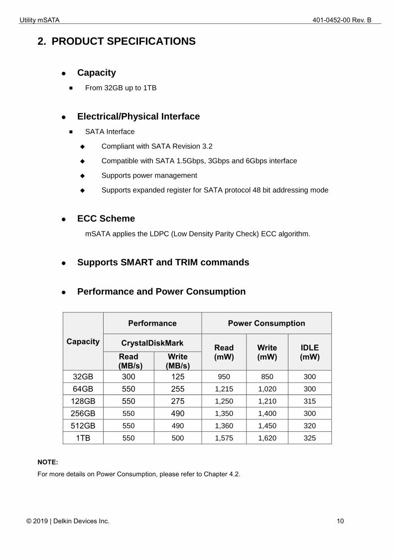
2. PRODUCT SPECIFICATIONS
⚫ Capacity
■ From 32GB up to 1TB
⚫ Electrical/Physical Interface
■ SATA Interface
◆ Compliant with SATA Revision 3.2
◆ Compatible with SATA 1.5Gbps, 3Gbps and 6Gbps interface
◆ Supports power management
◆ Supports expanded register for SATA protocol 48 bit addressing mode
⚫ ECC Scheme
mSATA applies the LDPC (Low Density Parity Check) ECC algorithm.
⚫ Supports SMART and TRIM commands
⚫ Performance and Power Consumption
Capacity
Performance Power Consumption
CrystalDiskMark Read (mW)
Write (mW)
IDLE (mW) Read
(MB/s) Write
(MB/s)
32GB 300 125 950 850 300
64GB 550 255 1,215 1,020 300
128GB 550 275 1,250 1,210 315
256GB 550 490 1,350 1,400 300
512GB 550 490 1,360 1,450 320
1TB 550 500 1,575 1,620 325
NOTE:
For more details on Power Consumption, please refer to Chapter 4.2.
Utility mSATA 401-0452-00 Rev. B
© 2019 | Delkin Devices Inc. 11
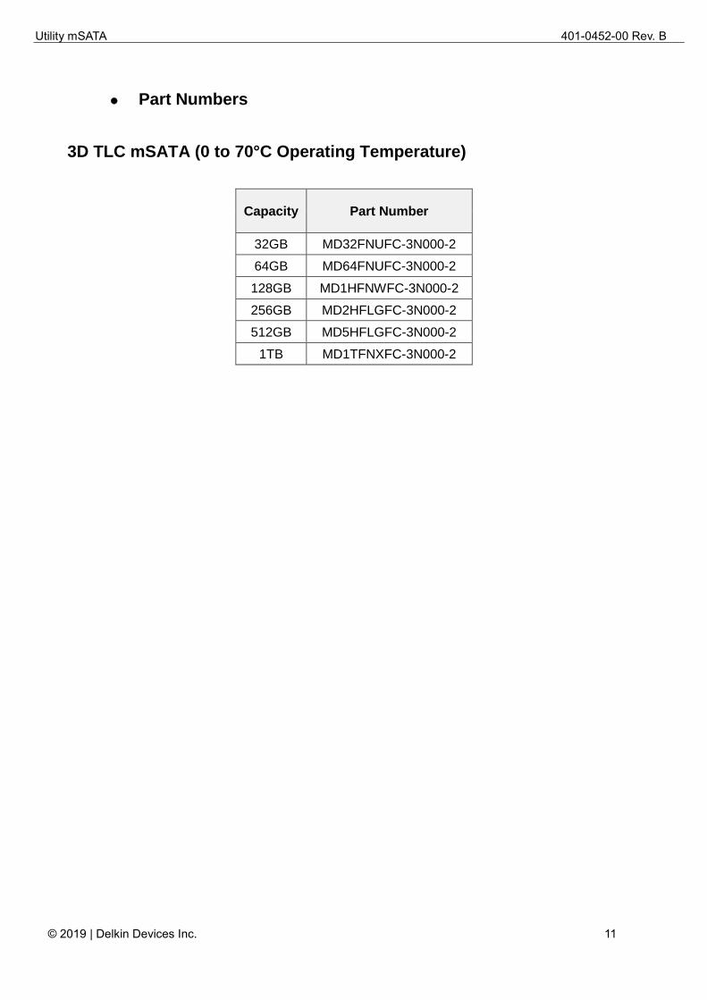
⚫ Part Numbers
3D TLC mSATA (0 to 70°C Operating Temperature)
Capacity Part Number
32GB MD32FNUFC-3N000-2
64GB MD64FNUFC-3N000-2
128GB MD1HFNWFC-3N000-2
256GB MD2HFLGFC-3N000-2
512GB MD5HFLGFC-3N000-2
1TB MD1TFNXFC-3N000-2
Utility mSATA 401-0452-00 Rev. B
© 2019 | Delkin Devices Inc. 12
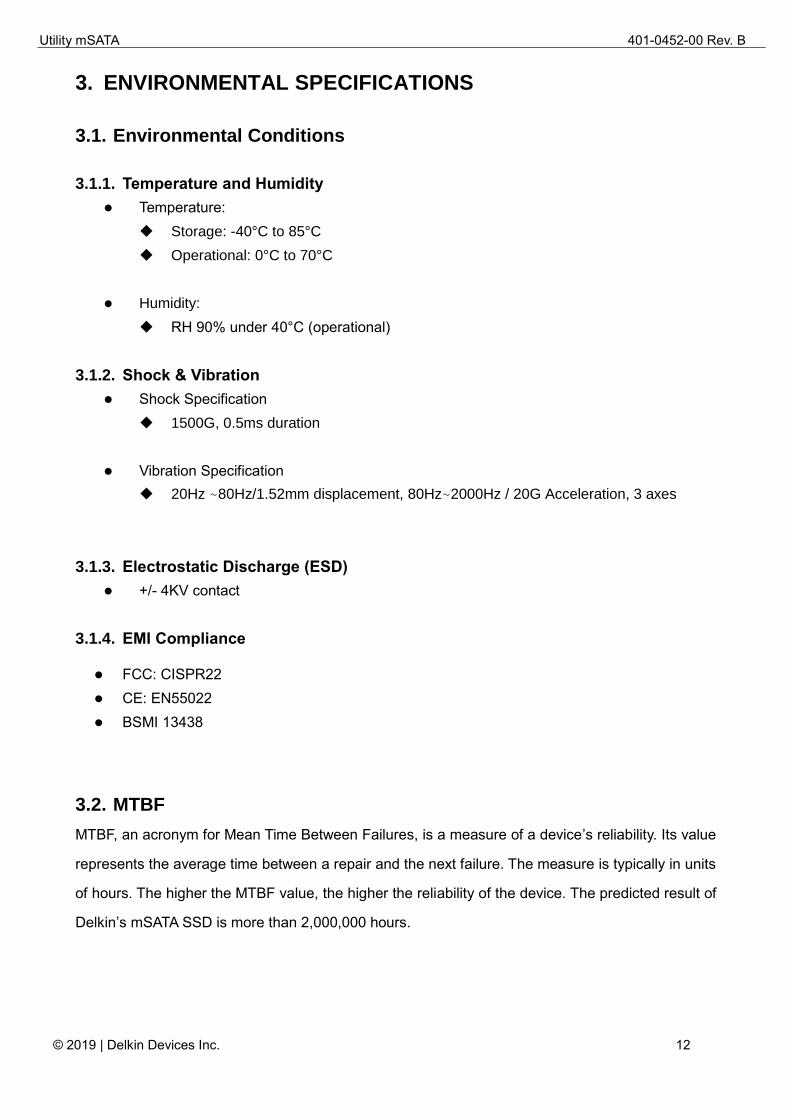
3. ENVIRONMENTAL SPECIFICATIONS
3.1. Environmental Conditions
3.1.1. Temperature and Humidity
⚫ Temperature:
◆ Storage: -40°C to 85°C
◆ Operational: 0°C to 70°C
⚫ Humidity:
◆ RH 90% under 40°C (operational)
3.1.2. Shock & Vibration
⚫ Shock Specification
◆ 1500G, 0.5ms duration
⚫ Vibration Specification
◆ 20Hz ~80Hz/1.52mm displacement, 80Hz~2000Hz / 20G Acceleration, 3 axes
3.1.3. Electrostatic Discharge (ESD)
⚫ +/- 4KV contact
3.1.4. EMI Compliance
⚫ FCC: CISPR22
⚫ CE: EN55022
⚫ BSMI 13438
3.2. MTBF
MTBF, an acronym for Mean Time Between Failures, is a measure of a device’s reliability. Its value
represents the average time between a repair and the next failure. The measure is typically in units
of hours. The higher the MTBF value, the higher the reliability of the device. The predicted result of
Delkin’s mSATA SSD is more than 2,000,000 hours.
Utility mSATA 401-0452-00 Rev. B
© 2019 | Delkin Devices Inc. 13
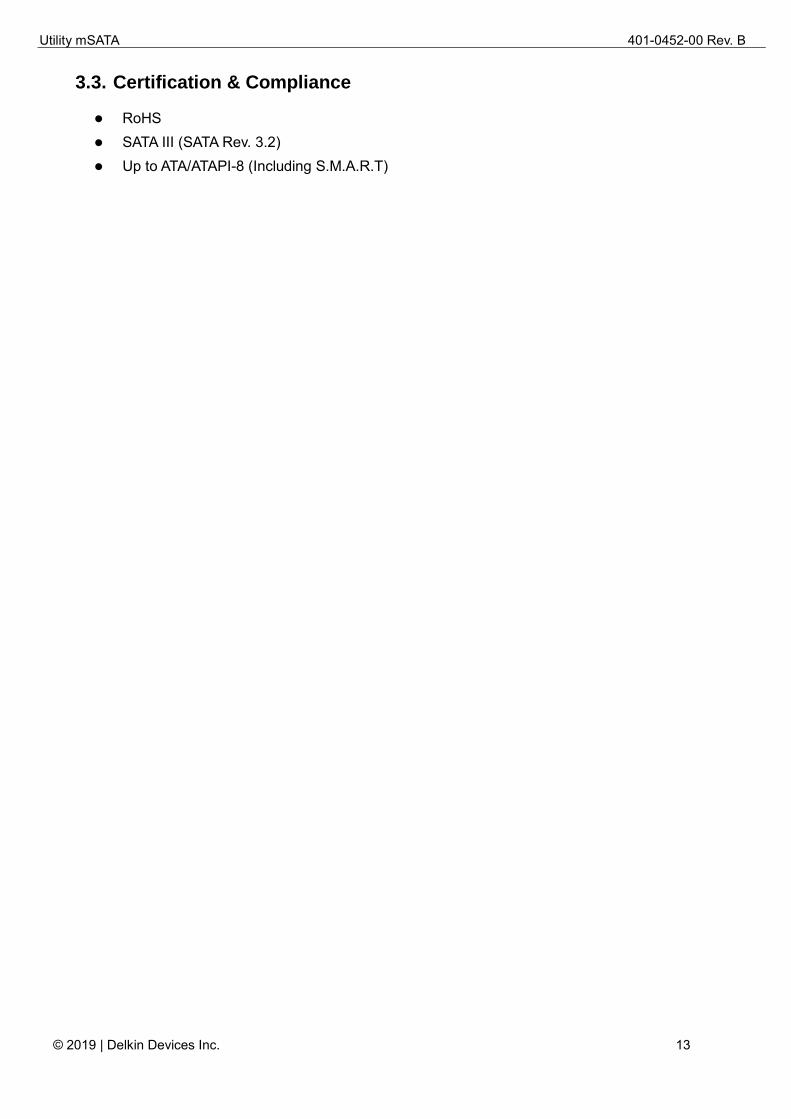
3.3. Certification & Compliance
⚫ RoHS
⚫ SATA III (SATA Rev. 3.2)
⚫ Up to ATA/ATAPI-8 (Including S.M.A.R.T)
Utility mSATA 401-0452-00 Rev. B
© 2019 | Delkin Devices Inc. 14
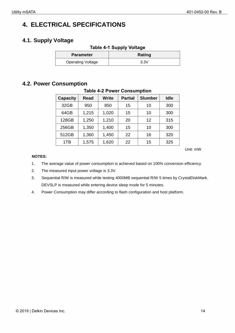
4. ELECTRICAL SPECIFICATIONS
4.1. Supply Voltage
Table 4-1 Supply Voltage
Parameter Rating
Operating Voltage 3.3V
4.2. Power Consumption
Table 4-2 Power Consumption
Capacity Read Write Partial Slumber Idle
32GB 950 850 15 10 300
64GB 1,215 1,020 15 10 300
128GB 1,250 1,210 20 12 315
256GB 1,350 1,400 15 10 300
512GB 1,360 1,450 22 16 320
1TB 1,575 1,620 22 15 325
Unit: mW
NOTES:
1. The average value of power consumption is achieved based on 100% conversion efficiency.
2. The measured input power voltage is 3.3V.
3. Sequential R/W is measured while testing 4000MB sequential R/W 5 times by CrystalDiskMark.
DEVSLP is measured while entering device sleep mode for 5 minutes.
4. Power Consumption may differ according to flash configuration and host platform.
Utility mSATA 401-0452-00 Rev. B
© 2019 | Delkin Devices Inc. 15
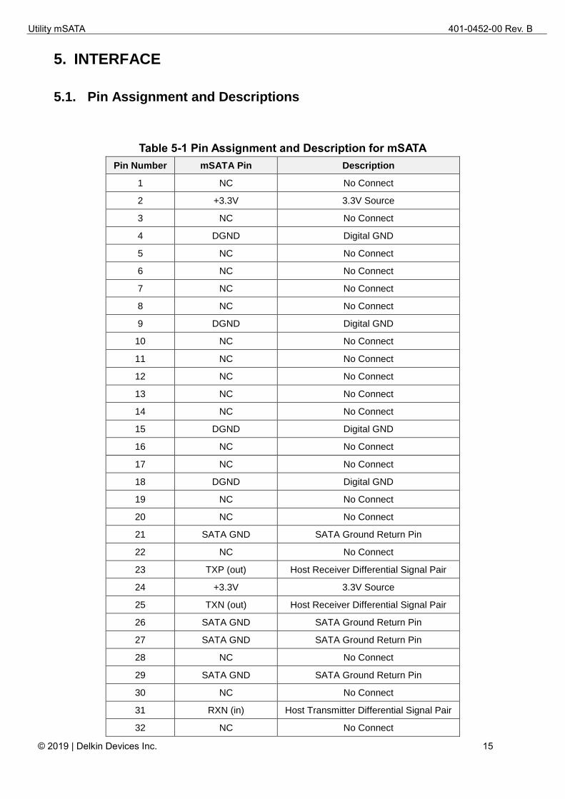
5. INTERFACE
5.1. Pin Assignment and Descriptions
Table 5-1 Pin Assignment and Description for mSATA
Pin Number mSATA Pin Description
1 NC No Connect
2 +3.3V 3.3V Source
3 NC No Connect
4 DGND Digital GND
5 NC No Connect
6 NC No Connect
7 NC No Connect
8 NC No Connect
9 DGND Digital GND
10 NC No Connect
11 NC No Connect
12 NC No Connect
13 NC No Connect
14 NC No Connect
15 DGND Digital GND
16 NC No Connect
17 NC No Connect
18 DGND Digital GND
19 NC No Connect
20 NC No Connect
21 SATA GND SATA Ground Return Pin
22 NC No Connect
23 TXP (out) Host Receiver Differential Signal Pair
24 +3.3V 3.3V Source
25 TXN (out) Host Receiver Differential Signal Pair
26 SATA GND SATA Ground Return Pin
27 SATA GND SATA Ground Return Pin
28 NC No Connect
29 SATA GND SATA Ground Return Pin
30 NC No Connect
31 RXN (in) Host Transmitter Differential Signal Pair
32 NC No Connect
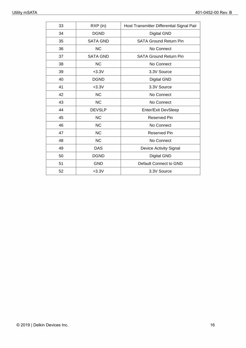
Utility mSATA 401-0452-00 Rev. B
© 2019 | Delkin Devices Inc. 16
33 RXP (in) Host Transmitter Differential Signal Pair
34 DGND Digital GND
35 SATA GND SATA Ground Return Pin
36 NC No Connect
37 SATA GND SATA Ground Return Pin
38 NC No Connect
39 +3.3V 3.3V Source
40 DGND Digital GND
41 +3.3V 3.3V Source
42 NC No Connect
43 NC No Connect
44 DEVSLP Enter/Exit DevSleep
45 NC Reserved Pin
46 NC No Connect
47 NC Reserved Pin
48 NC No Connect
49 DAS Device Activity Signal
50 DGND Digital GND
51 GND Default Connect to GND
52 +3.3V 3.3V Source
Utility mSATA 401-0452-00 Rev. B
© 2019 | Delkin Devices Inc. 17
6. SUPPORTED COMMANDS
6.1. ATA Command List
Table 6-1 ATA Command List
Op Code Description Op Code Description
00h NOP C9h Read DMA without Retry
06h Data Set Management CAh Write DMA
10h-1Fh Recalibrate CBh Write DMA without Retry
20h Read Sectors CEh Write Multiple FUA EXT
21h Read Sectors without Retry E0h Standby Immediate
24h Read Sectors EXT E1h Idle Immediate
25h Read DMA EXT E2h Standby
27h Read Native Max Address EXT E3h Idle
29h Read Multiple EXT E4h Read Buffer
2Fh Read Log EXT E5h Check Power Mode
30h Write Sectors E6h Sleep
31h Write Sectors without Retry E7h Flush Cache
34h Write Sectors EXT E8h Write Buffer
35h Write DMA EXT E9h READ BUFFER DMA
37h Set Native Max Address EXT EAh Flush Cache EXT
38h CFA WRITE SECTORS WITHOUT
ERASE EBh Write Buffer DMA
39h Write Multiple EXT ECh Identity Device
3Dh Write DMA FUA EXT EFh Set Features
3Fh Write Long EXT EFh 02h Enable volatile write cache
40h Read Verify Sectors EFh 03h Set Transfer mode
41h Read Verify Sectors without Retry EFh 05h Enable the APM feature set
42h Read Verify Sectors EXT EFh 10h Enable use of SATA features
set
44h Zero EXT EFh 10h 02h Enable DMA Setup FIS Auto-
Activate optimization
45h WRITE UNCORRECTABLE EXT EFh 10h 03h
Enable Device-initiated
interface power state (DIPM)
transitions
47h Red Log DMA EXT EFh 10h 06h Enable Software Settings
Preservation (SSP)
57h Write Log DMA EXT EFh 10h 07h Enable Device Automatic
Partial to Slumber transitions
Utility mSATA 401-0452-00 Rev. B
© 2019 | Delkin Devices Inc. 18
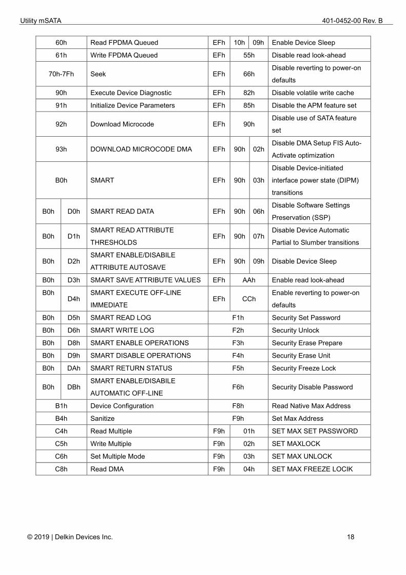
60h Read FPDMA Queued EFh 10h 09h Enable Device Sleep
61h Write FPDMA Queued EFh 55h Disable read look-ahead
70h-7Fh Seek EFh 66h Disable reverting to power-on
defaults
90h Execute Device Diagnostic EFh 82h Disable volatile write cache
91h Initialize Device Parameters EFh 85h Disable the APM feature set
92h Download Microcode EFh 90h Disable use of SATA feature
set
93h DOWNLOAD MICROCODE DMA EFh 90h 02h Disable DMA Setup FIS Auto-
Activate optimization
B0h SMART EFh 90h 03h
Disable Device-initiated
interface power state (DIPM)
transitions
B0h D0h SMART READ DATA EFh 90h 06h Disable Software Settings
Preservation (SSP)
B0h D1h SMART READ ATTRIBUTE
THRESHOLDS EFh 90h 07h
Disable Device Automatic
Partial to Slumber transitions
B0h D2h SMART ENABLE/DISABILE
ATTRIBUTE AUTOSAVE EFh 90h 09h Disable Device Sleep
B0h D3h SMART SAVE ATTRIBUTE VALUES EFh AAh Enable read look-ahead
B0h D4h
SMART EXECUTE OFF-LINE
IMMEDIATE EFh CCh
Enable reverting to power-on
defaults
B0h D5h SMART READ LOG F1h Security Set Password
B0h D6h SMART WRITE LOG F2h Security Unlock
B0h D8h SMART ENABLE OPERATIONS F3h Security Erase Prepare
B0h D9h SMART DISABLE OPERATIONS F4h Security Erase Unit
B0h DAh SMART RETURN STATUS F5h Security Freeze Lock
B0h DBh SMART ENABLE/DISABILE
AUTOMATIC OFF-LINE F6h Security Disable Password
B1h Device Configuration F8h Read Native Max Address
B4h Sanitize F9h Set Max Address
C4h Read Multiple F9h 01h SET MAX SET PASSWORD
C5h Write Multiple F9h 02h SET MAXLOCK
C6h Set Multiple Mode F9h 03h SET MAX UNLOCK
C8h Read DMA F9h 04h SET MAX FREEZE LOCIK
Utility mSATA 401-0452-00 Rev. B
© 2019 | Delkin Devices Inc. 19
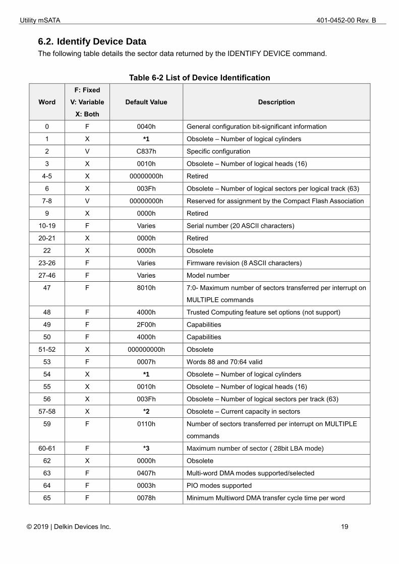
6.2. Identify Device Data
The following table details the sector data returned by the IDENTIFY DEVICE command.
Table 6-2 List of Device Identification
Word
F: Fixed
V: Variable
X: Both
Default Value Description
0 F 0040h General configuration bit-significant information
1 X *1 Obsolete – Number of logical cylinders
2 V C837h Specific configuration
3 X 0010h Obsolete – Number of logical heads (16)
4-5 X 00000000h Retired
6 X 003Fh Obsolete – Number of logical sectors per logical track (63)
7-8 V 00000000h Reserved for assignment by the Compact Flash Association
9 X 0000h Retired
10-19 F Varies Serial number (20 ASCII characters)
20-21 X 0000h Retired
22 X 0000h Obsolete
23-26 F Varies Firmware revision (8 ASCII characters)
27-46 F Varies Model number
47 F 8010h 7:0- Maximum number of sectors transferred per interrupt on
MULTIPLE commands
48 F 4000h Trusted Computing feature set options (not support)
49 F 2F00h Capabilities
50 F 4000h Capabilities
51-52 X 000000000h Obsolete
53 F 0007h Words 88 and 70:64 valid
54 X *1 Obsolete – Number of logical cylinders
55 X 0010h Obsolete – Number of logical heads (16)
56 X 003Fh Obsolete – Number of logical sectors per track (63)
57-58 X *2 Obsolete – Current capacity in sectors
59 F 0110h Number of sectors transferred per interrupt on MULTIPLE
commands
60-61 F *3 Maximum number of sector ( 28bit LBA mode)
62 X 0000h Obsolete
63 F 0407h Multi-word DMA modes supported/selected
64 F 0003h PIO modes supported
65 F 0078h Minimum Multiword DMA transfer cycle time per word
Utility mSATA 401-0452-00 Rev. B
© 2019 | Delkin Devices Inc. 20
Word
F: Fixed
V: Variable
X: Both
Default Value Description
66 F 0078h Manufacturer’s recommended Multiword DMA transfer cycle
time
67 F 0078h Minimum PIO transfer cycle time without flow control
68 F 0078h Minimum PIO transfer cycle time with IORDY flow control
69 F 0100h Additional Supported (support download microcode DMA)
70 F 0000h Reserved
71-74 F 0000000000000000h Reserved for the IDENTIFY PACKET DEVICE command
75 F 001Fh Queue depth
76 F 670eh Serial SATA capabilities
77 F 0084h Serial ATA Additional Capabilities
78 F 014Ch Serial ATA features supported
79 V 0040h Serial ATA features enabled
80 F 07F8h Major Version Number
81 F 0000h Minor Version Number
82 F 346bh Command set supported
83 F 7d09h Command set supported
84 F 6063h Command set/feature supported extension
85 V 3469h Command set/feature enabled
86 V bc01h Command set/feature enabled
87 V 6063h Command set/feature default
88 V 003Fh Ultra DMA Modes
89 F 0001h Time required for security erase unit completion
90 F 001Eh Time required for Enhanced security erase completion
91 V 0000h Current advanced power management value
92 V FFFEh Master Password Revision Code
93 F 0000h Hardware reset result. For SATA devices, word 93 shall be
set to the value 0000h.
94 V 0000h Obsolete
95 F 0000h Stream Minimum Request Size
96 V 0000h Streaming Transfer Time – DMA
97 V 0000h Streaming Access Latency – DMA and PIO
98-99 F 0000h Streaming Performance Granularity
100-103 V *4 Maximum user LBA for 48 bit Address feature set
104 V 0000h Streaming Transfer Time – PIO
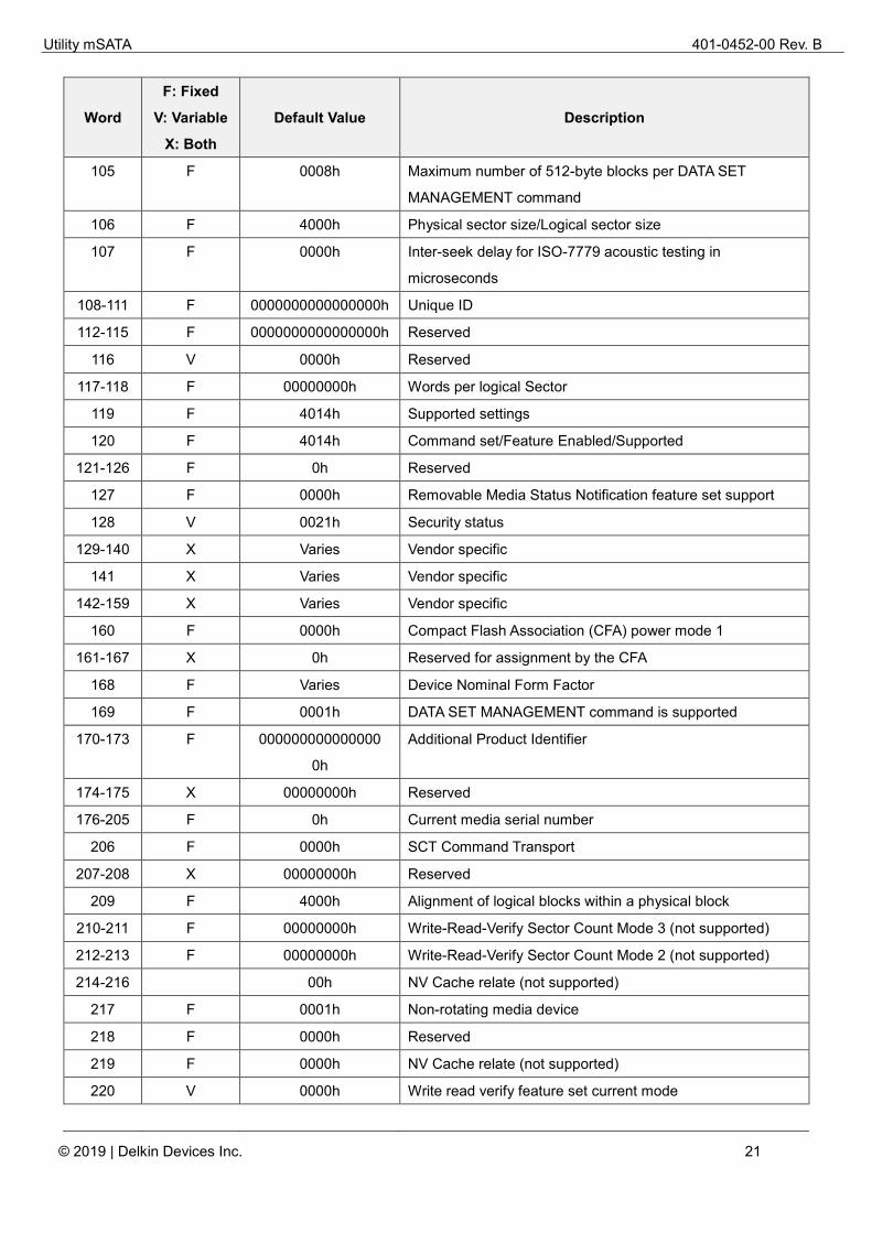
Utility mSATA 401-0452-00 Rev. B
© 2019 | Delkin Devices Inc. 21
Word
F: Fixed
V: Variable
X: Both
Default Value Description
105 F 0008h Maximum number of 512-byte blocks per DATA SET
MANAGEMENT command
106 F 4000h Physical sector size/Logical sector size
107 F 0000h Inter-seek delay for ISO-7779 acoustic testing in
microseconds
108-111 F 0000000000000000h Unique ID
112-115 F 0000000000000000h Reserved
116 V 0000h Reserved
117-118 F 00000000h Words per logical Sector
119 F 4014h Supported settings
120 F 4014h Command set/Feature Enabled/Supported
121-126 F 0h Reserved
127 F 0000h Removable Media Status Notification feature set support
128 V 0021h Security status
129-140 X Varies Vendor specific
141 X Varies Vendor specific
142-159 X Varies Vendor specific
160 F 0000h Compact Flash Association (CFA) power mode 1
161-167 X 0h Reserved for assignment by the CFA
168 F Varies Device Nominal Form Factor
169 F 0001h DATA SET MANAGEMENT command is supported
170-173 F 000000000000000
0h
Additional Product Identifier
174-175 X 00000000h Reserved
176-205 F 0h Current media serial number
206 F 0000h SCT Command Transport
207-208 X 00000000h Reserved
209 F 4000h Alignment of logical blocks within a physical block
210-211 F 00000000h Write-Read-Verify Sector Count Mode 3 (not supported)
212-213 F 00000000h Write-Read-Verify Sector Count Mode 2 (not supported)
214-216 00h NV Cache relate (not supported)
217 F 0001h Non-rotating media device
218 F 0000h Reserved
219 F 0000h NV Cache relate (not supported)
220 V 0000h Write read verify feature set current mode
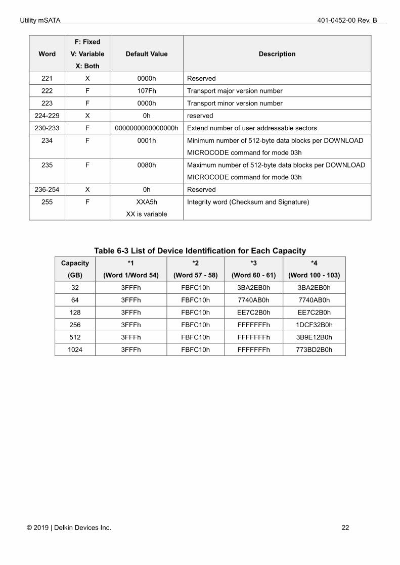
Utility mSATA 401-0452-00 Rev. B
© 2019 | Delkin Devices Inc. 22
Word
F: Fixed
V: Variable
X: Both
Default Value Description
221 X 0000h Reserved
222 F 107Fh Transport major version number
223 F 0000h Transport minor version number
224-229 X 0h reserved
230-233 F 0000000000000000h Extend number of user addressable sectors
234 F 0001h Minimum number of 512-byte data blocks per DOWNLOAD
MICROCODE command for mode 03h
235 F 0080h Maximum number of 512-byte data blocks per DOWNLOAD
MICROCODE command for mode 03h
236-254 X 0h Reserved
255 F XXA5h
XX is variable
Integrity word (Checksum and Signature)
Table 6-3 List of Device Identification for Each Capacity
Capacity
(GB)
*1
(Word 1/Word 54)
*2
(Word 57 - 58)
*3
(Word 60 - 61)
*4
(Word 100 - 103)
32 3FFFh FBFC10h 3BA2EB0h 3BA2EB0h
64 3FFFh FBFC10h 7740AB0h 7740AB0h
128 3FFFh FBFC10h EE7C2B0h EE7C2B0h
256 3FFFh FBFC10h FFFFFFFh 1DCF32B0h
512 3FFFh FBFC10h FFFFFFFh 3B9E12B0h
1024 3FFFh FBFC10h FFFFFFFh 773BD2B0h
Utility mSATA 401-0452-00 Rev. B
© 2019 | Delkin Devices Inc. 23
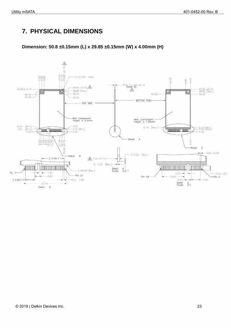
7. PHYSICAL DIMENSIONS
Dimension: 50.8 ±0.15mm (L) x 29.85 ±0.15mm (W) x 4.00mm (H)