Embed Size (px)
Citation preview
Eur. Phys. J. Appl. Phys. 43, 1–18 (2008)DOI: 10.1051/epjap:2008143 THE EUROPEAN
PHYSICAL JOURNALAPPLIED PHYSICS
Resonant terahertz transmission in plasmonic arraysof subwavelength holes
W. Zhanga
School of Electrical and Computer Engineering, Oklahoma State University, Stillwater, 74078 Oklahoma, USA
Received: 1st May 2008 / Accepted: 17 June 2008Published online: 4 July 2008 – c© EDP Sciences
Abstract. A review of transmission properties of two-dimensional plasmonic structures in the terahertzregime is presented. Resonant terahertz transmission was demonstrated in arrays of subwavelength holespatterned on both metals and semiconductors. The effects of hole shape, hole dimensions, dielectric func-tion of metals, array film thickness, and a dielectric overlayer were investigated by the state-of-the-artterahertz spectroscopy modalities. Extraordinary terahertz transmission was demonstrated in arrays ofsubwavelength holes made even from Pb, a generally poor metal, and having optically thin thicknessesless than one-third of a skin depth. We also observed a direct transition of a surface plasmon resonancefrom a photonic crystal minimum in a photo-doped semiconductor array. According to the Fano model,transmission properties of such plasmonic arrays are characterized by two essential contributions: resonantexcitation of surface plasmons and nonresonant direct transmission. Plasmonic structures will find fasci-nating applications in terahertz imaging, biomedical sensing, subwavelength terahertz spectroscopy, andintegrated terahertz devices.
PACS. 73.20.Mf Collective excitations (including excitons, polarons, plasmons and other charge-densityexcitations) – 78.47.+p Time-resolved optical spectroscopies and other ultrafast optical measurements incondensed matter – 42.79.Ag Apertures, collimators
1 Introduction
Two-dimensional (2D) array of subwavelength holes,which enables extraordinary transmission of electromag-netic waves, has become a unique component in integratednano- and micro-photonics and may find breakthrough ap-plications in semiconductor nanofabrication, microscopy,display technology, and bio-chemical sensing [1–3]. Un-derstanding the physical origin of resonant properties insuch plasmonic structures has attracted significant inter-est in a broad spectrum of electromagnetic waves. Sur-face plasmons (SPs) are collective excitations for quan-tized oscillations of electrons [4]. The resonant interactionbetween electron-charged oscillations near the surface ofmetal and the electromagnetic field creates SPs and resultsin rather unique properties [5]. Recent advance in extraor-dinary transmission of light has demonstrated when lightpassed through periodic subwavelength holes perforatedin a metallic film, the resulted higher-than-unity trans-mission was primarily attributed to resonant excitation ofSPs [1,3]. Light was coupled into the holes in the form ofSPs which were squeezed through the holes and then con-verted back into light on the far side of the holes. Extensiveexperimental and theoretical studies have been carried out
a e-mail: [email protected]
to approach fundamental understanding of this extraordi-nary transmission and to explore its potential applicationsin a broad range of disciplines [6–9].
In the terahertz regime, SPs have recently at-tracted much attention and become an attractive newarea [10–19]. Due to a drastic increase in the value of di-electric function εm = εrm + iεim, most metals becomehighly conductive at terahertz frequencies. This has re-sulted in discrepancies in SP-enhanced transmission of ter-ahertz radiation with that in the visible spectral regime.Experimental results on transmission properties of lightin metallic structures have indicated that SP-enhancedtransmission is normally achieved in metals with largeratio of the real to the imaginary dielectric constant,−εrm/εim � 1 [20,21]. In the terahertz regime, however,this ratio becomes −εrm/εim < 1 for non-transition met-als, such as Ag, Au, Cu, and Al [22]. This was consideredas a limitation to realize resonant excitation of terahertzSPs in the periodic subwavelength structures. The recentstudies, however, have demonstrated that an appropriatesurface corrugation provided by the subwavelength struc-tures could facilitate the resonant excitation of SPs evenwith −εrm/εim < 1 [23]. SP-enhanced terahertz transmis-sion has been experimentally observed in subwavelengthhole arrays patterned in metal films made from both goodand generally poor metals [24,25].
Article published by EDP Sciences
2 The European Physical Journal Applied Physics
In addition to metals, semiconductors with high den-sity of free carriers exhibit metallic properties by havinga negative real part of dielectric function (εrm < 0), andthus can be used as alternate metallic media to supportSPs at terahertz frequencies. As a result, enhanced tera-hertz transmission was demonstrated in microstructuredhole arrays made from both intrinsically doped and photo-doped semiconductors [11,26–30]. The advantage of semi-conductors is that their dielectric function can be modifiedby varying doping concentration, temperature, or opticalexcitation. This in turn enables tuning and switching ofSPs. Such semiconductor plasmonic arrays may find appli-cations in all solid state terahertz optoelectronic devices,such as high-throughput, high resolution filters, and fo-cusing elements for terahertz imaging system.
The combination of SPs and terahertz spectroscopywill be a fruitful field both in fundamental understand-ing the properties of terahertz SPs and their promisingapplications. In this article, we present our recent workon resonant terahertz transmission in lithographically fab-ricated 2D metal and semiconductor arrays of subwave-length holes. The presentation is organized as follows: inSection 2, we describe experimental methods employedin these studies, including terahertz time-domain spec-troscopy and optical pump-terahertz probe spectroscopy.In Section 3, the lithographic fabrication processes of theplasmonic arrays are presented. In Section 4, we reviewresonant terahertz transmission in metal arrays of sub-wavelength holes. The interesting properties of plasmonicstructures made from semiconductors are introduced inSection 5. Finally, a conclusion is drawn in Section 6.
2 Experimental methods
2.1 Terahertz time-domain spectroscopy
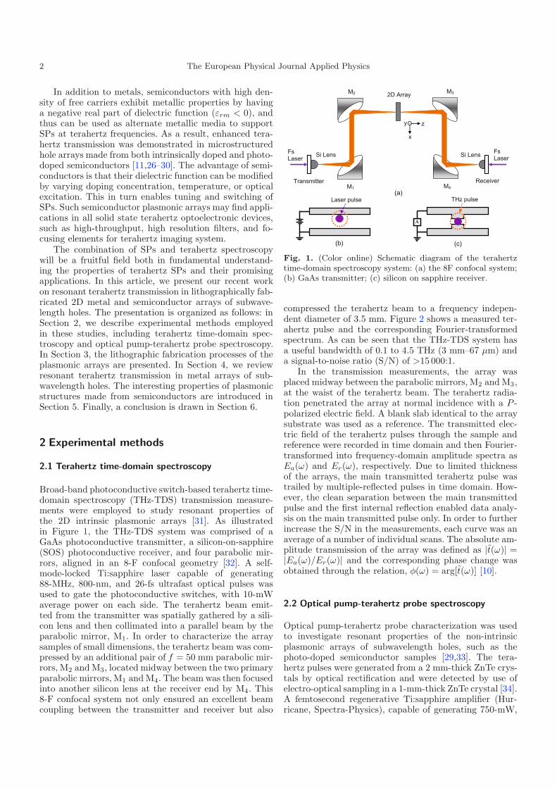
Broad-band photoconductive switch-based terahertz time-domain spectroscopy (THz-TDS) transmission measure-ments were employed to study resonant properties ofthe 2D intrinsic plasmonic arrays [31]. As illustratedin Figure 1, the THz-TDS system was comprised of aGaAs photoconductive transmitter, a silicon-on-sapphire(SOS) photoconductive receiver, and four parabolic mir-rors, aligned in an 8-F confocal geometry [32]. A self-mode-locked Ti:sapphire laser capable of generating88-MHz, 800-nm, and 26-fs ultrafast optical pulses wasused to gate the photoconductive switches, with 10-mWaverage power on each side. The terahertz beam emit-ted from the transmitter was spatially gathered by a sili-con lens and then collimated into a parallel beam by theparabolic mirror, M1. In order to characterize the arraysamples of small dimensions, the terahertz beam was com-pressed by an additional pair of f = 50 mm parabolic mir-rors, M2 and M3, located midway between the two primaryparabolic mirrors, M1 and M4. The beam was then focusedinto another silicon lens at the receiver end by M4. This8-F confocal system not only ensured an excellent beamcoupling between the transmitter and receiver but also
A
THz pulse
(c)
Laser pulse
(b)
FsLaser
FsLaser
Transmitter Receiver
Si Lens
M2 M32D Array
M1 M4
Si Lens
y z
x
(a)
Fig. 1. (Color online) Schematic diagram of the terahertztime-domain spectroscopy system: (a) the 8F confocal system;(b) GaAs transmitter; (c) silicon on sapphire receiver.
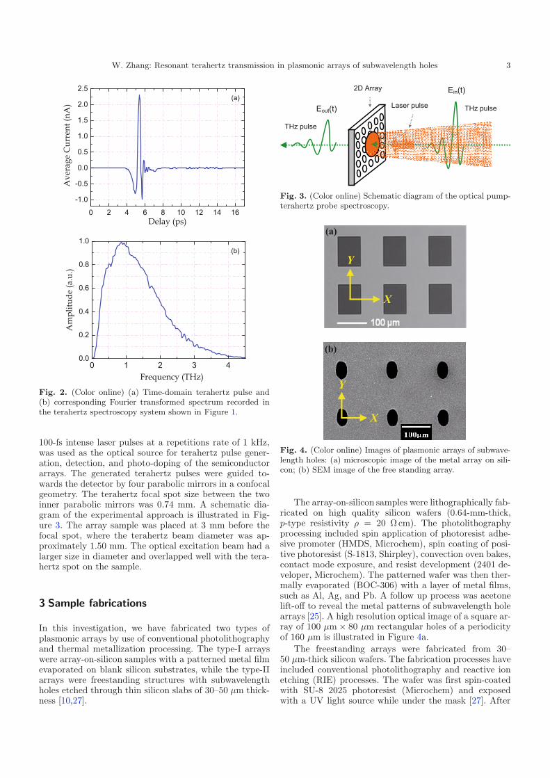
compressed the terahertz beam to a frequency indepen-dent diameter of 3.5 mm. Figure 2 shows a measured ter-ahertz pulse and the corresponding Fourier-transformedspectrum. As can be seen that the THz-TDS system hasa useful bandwidth of 0.1 to 4.5 THz (3 mm–67 μm) anda signal-to-noise ratio (S/N) of >15 000:1.
In the transmission measurements, the array wasplaced midway between the parabolic mirrors, M2 and M3,at the waist of the terahertz beam. The terahertz radia-tion penetrated the array at normal incidence with a P -polarized electric field. A blank slab identical to the arraysubstrate was used as a reference. The transmitted elec-tric field of the terahertz pulses through the sample andreference were recorded in time domain and then Fourier-transformed into frequency-domain amplitude spectra asEa(ω) and Er(ω), respectively. Due to limited thicknessof the arrays, the main transmitted terahertz pulse wastrailed by multiple-reflected pulses in time domain. How-ever, the clean separation between the main transmittedpulse and the first internal reflection enabled data analy-sis on the main transmitted pulse only. In order to furtherincrease the S/N in the measurements, each curve was anaverage of a number of individual scans. The absolute am-plitude transmission of the array was defined as |t(ω)| =|Ea(ω)/Er(ω)| and the corresponding phase change wasobtained through the relation, φ(ω) = arg[t(ω)] [10].
2.2 Optical pump-terahertz probe spectroscopy
Optical pump-terahertz probe characterization was usedto investigate resonant properties of the non-intrinsicplasmonic arrays of subwavelength holes, such as thephoto-doped semiconductor samples [29,33]. The tera-hertz pulses were generated from a 2 mm-thick ZnTe crys-tals by optical rectification and were detected by use ofelectro-optical sampling in a 1-mm-thick ZnTe crystal [34].A femtosecond regenerative Ti:sapphire amplifier (Hur-ricane, Spectra-Physics), capable of generating 750-mW,
W. Zhang: Resonant terahertz transmission in plasmonic arrays of subwavelength holes 3
0 2 4 6 8 10 12 14 16
-1.0
-0.5
0.0
0.5
1.0
1.5
2.0
2.5(a)
Ave
rage
Cur
rent
(nA
)
Delay (ps)
0 1 2 3 40.0
0.2
0.4
0.6
0.8
1.0(b)
Am
plitu
de (a
.u.)
Frequency (THz)
Fig. 2. (Color online) (a) Time-domain terahertz pulse and(b) corresponding Fourier transformed spectrum recorded inthe terahertz spectroscopy system shown in Figure 1.
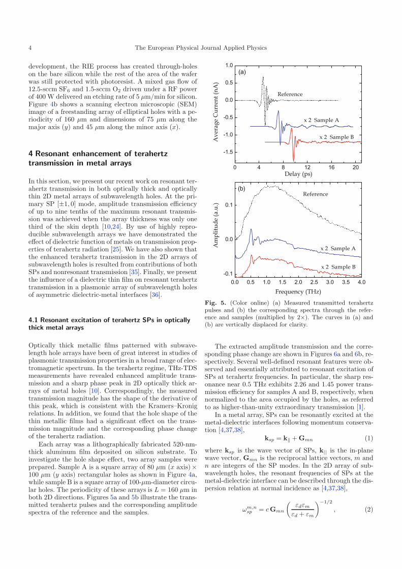
100-fs intense laser pulses at a repetitions rate of 1 kHz,was used as the optical source for terahertz pulse gener-ation, detection, and photo-doping of the semiconductorarrays. The generated terahertz pulses were guided to-wards the detector by four parabolic mirrors in a confocalgeometry. The terahertz focal spot size between the twoinner parabolic mirrors was 0.74 mm. A schematic dia-gram of the experimental approach is illustrated in Fig-ure 3. The array sample was placed at 3 mm before thefocal spot, where the terahertz beam diameter was ap-proximately 1.50 mm. The optical excitation beam had alarger size in diameter and overlapped well with the tera-hertz spot on the sample.
3 Sample fabrications
In this investigation, we have fabricated two types ofplasmonic arrays by use of conventional photolithographyand thermal metallization processing. The type-I arrayswere array-on-silicon samples with a patterned metal filmevaporated on blank silicon substrates, while the type-IIarrays were freestanding structures with subwavelengthholes etched through thin silicon slabs of 30–50 μm thick-ness [10,27].
THz pulse
Eout(t)
2D Array Ein(t)
Laser pulse THz pulse
Fig. 3. (Color online) Schematic diagram of the optical pump-terahertz probe spectroscopy.
X
Y
(a)
(b)
X
Y
Fig. 4. (Color online) Images of plasmonic arrays of subwave-length holes: (a) microscopic image of the metal array on sili-con; (b) SEM image of the free standing array.
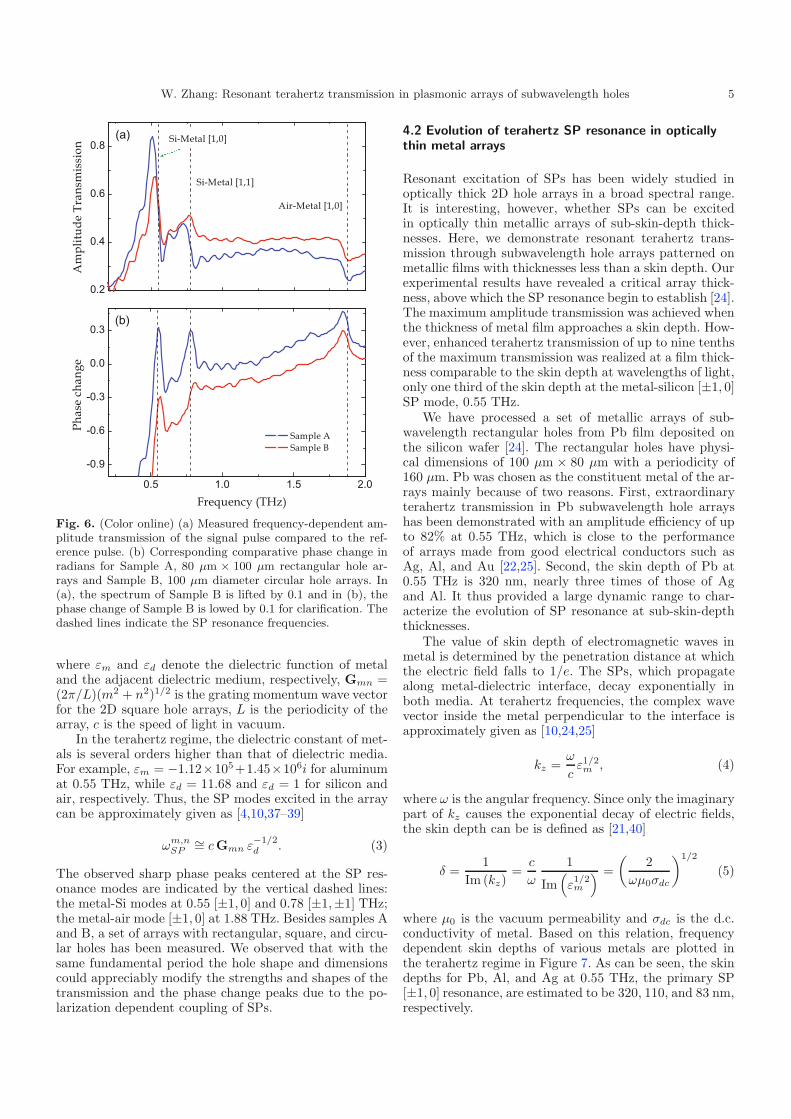
The array-on-silicon samples were lithographically fab-ricated on high quality silicon wafers (0.64-mm-thick,p-type resistivity ρ = 20 Ωcm). The photolithographyprocessing included spin application of photoresist adhe-sive promoter (HMDS, Microchem), spin coating of posi-tive photoresist (S-1813, Shirpley), convection oven bakes,contact mode exposure, and resist development (2401 de-veloper, Microchem). The patterned wafer was then ther-mally evaporated (BOC-306) with a layer of metal films,such as Al, Ag, and Pb. A follow up process was acetonelift-off to reveal the metal patterns of subwavelength holearrays [25]. A high resolution optical image of a square ar-ray of 100 μm × 80 μm rectangular holes of a periodicityof 160 μm is illustrated in Figure 4a.
The freestanding arrays were fabricated from 30–50 μm-thick silicon wafers. The fabrication processes haveincluded conventional photolithography and reactive ionetching (RIE) processes. The wafer was first spin-coatedwith SU-8 2025 photoresist (Microchem) and exposedwith a UV light source while under the mask [27]. After
4 The European Physical Journal Applied Physics
development, the RIE process has created through-holeson the bare silicon while the rest of the area of the waferwas still protected with photoresist. A mixed gas flow of12.5-sccm SF6 and 1.5-sccm O2 driven under a RF powerof 400 W delivered an etching rate of 5 μm/min for silicon.Figure 4b shows a scanning electron microscopic (SEM)image of a freestanding array of elliptical holes with a pe-riodicity of 160 μm and dimensions of 75 μm along themajor axis (y) and 45 μm along the minor axis (x).
4 Resonant enhancement of terahertztransmission in metal arrays
In this section, we present our recent work on resonant ter-ahertz transmission in both optically thick and opticallythin 2D metal arrays of subwavelength holes. At the pri-mary SP [±1, 0] mode, amplitude transmission efficiencyof up to nine tenths of the maximum resonant transmis-sion was achieved when the array thickness was only onethird of the skin depth [10,24]. By use of highly repro-ducible subwavelength arrays we have demonstrated theeffect of dielectric function of metals on transmission prop-erties of terahertz radiation [25]. We have also shown thatthe enhanced terahertz transmission in the 2D arrays ofsubwavelength holes is resulted from contributions of bothSPs and nonresonant transmission [35]. Finally, we presentthe influence of a dielectric thin film on resonant terahertztransmission in a plasmonic array of subwavelength holesof asymmetric dielectric-metal interfaces [36].
4.1 Resonant excitation of terahertz SPs in opticallythick metal arrays
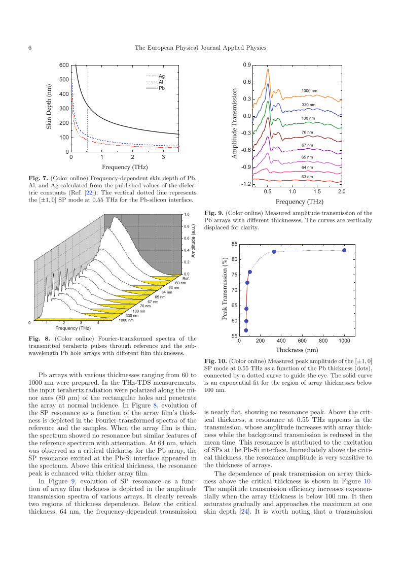
Optically thick metallic films patterned with subwave-length hole arrays have been of great interest in studies ofplasmonic transmission properties in a broad range of elec-tromagnetic spectrum. In the terahertz regime, THz-TDSmeasurements have revealed enhanced amplitude trans-mission and a sharp phase peak in 2D optically thick ar-rays of metal holes [10]. Correspondingly, the measuredtransmission magnitude has the shape of the derivative ofthis peak, which is consistent with the Kramers–Kronigrelations. In addition, we found that the hole shape of thethin metallic films had a significant effect on the trans-mission magnitude and the corresponding phase changeof the terahertz radiation.
Each array was a lithographically fabricated 520-nm-thick aluminum film deposited on silicon substrate. Toinvestigate the hole shape effect, two array samples wereprepared. Sample A is a square array of 80 μm (x axis)×100 μm (y axis) rectangular holes as shown in Figure 4a,while sample B is a square array of 100-μm-diameter circu-lar holes. The periodicity of these arrays is L = 160 μm inboth 2D directions. Figures 5a and 5b illustrate the trans-mitted terahertz pulses and the corresponding amplitudespectra of the reference and the samples.
0 4 8 12 16 20
-1.5
-1.0
-0.5
0.0
0.5
1.0
0.0 0.5 1.0 1.5 2.0 2.5 3.0 3.5 4.0-0.1
0.0
0.1
(a)
x 2 Sample B
x 2 Sample B
x 2 Sample A
Reference
Delay (ps)
Ave
rage
Cur
rent
(nA
)
(b)
x 2 Sample A
Reference
Frequency (THz)
Am
plitu
de (a
.u.)
Fig. 5. (Color online) (a) Measured transmitted terahertzpulses and (b) the corresponding spectra through the refer-ence and samples (multiplied by 2×). The curves in (a) and(b) are vertically displaced for clarity.
The extracted amplitude transmission and the corre-sponding phase change are shown in Figures 6a and 6b, re-spectively. Several well-defined resonant features were ob-served and essentially attributed to resonant excitation ofSPs at terahertz frequencies. In particular, the sharp res-onance near 0.5 THz exhibits 2.26 and 1.45 power trans-mission efficiency for samples A and B, respectively, whennormalized to the area occupied by the holes, as referredto as higher-than-unity extraordinary transmission [1].
In a metal array, SPs can be resonantly excited at themetal-dielectric interfaces following momentum conserva-tion [4,37,38],
ksp = k‖ + Gmn (1)
where ksp is the wave vector of SPs, k|| is the in-planewave vector, Gmn is the reciprocal lattice vectors, m andn are integers of the SP modes. In the 2D array of sub-wavelength holes, the resonant frequencies of SPs at themetal-dielectric interface can be described through the dis-persion relation at normal incidence as [4,37,38],
ωm,nsp = cGmn
(εdεm
εd + εm
)−1/2
, (2)
W. Zhang: Resonant terahertz transmission in plasmonic arrays of subwavelength holes 5
0.2
0.4
0.6
0.8
0.5 1.0 1.5 2.0
-0.9
-0.6
-0.3
0.0
0.3
Si-Metal [1,0]
Air-Metal [1,0]
Si-Metal [1,1]
(a)
Am
plitu
de T
rans
mis
sion
Sample A Sample B
(b)
Frequency (THz)
Phas
e ch
ange
Fig. 6. (Color online) (a) Measured frequency-dependent am-plitude transmission of the signal pulse compared to the ref-erence pulse. (b) Corresponding comparative phase change inradians for Sample A, 80 μm × 100 μm rectangular hole ar-rays and Sample B, 100 μm diameter circular hole arrays. In(a), the spectrum of Sample B is lifted by 0.1 and in (b), thephase change of Sample B is lowed by 0.1 for clarification. Thedashed lines indicate the SP resonance frequencies.
where εm and εd denote the dielectric function of metaland the adjacent dielectric medium, respectively, Gmn =(2π/L)(m2 + n2)1/2 is the grating momentum wave vectorfor the 2D square hole arrays, L is the periodicity of thearray, c is the speed of light in vacuum.
In the terahertz regime, the dielectric constant of met-als is several orders higher than that of dielectric media.For example, εm = −1.12×10⁵+1.45×10⁶i for aluminumat 0.55 THz, while εd = 11.68 and εd = 1 for silicon andair, respectively. Thus, the SP modes excited in the arraycan be approximately given as [4,10,37–39]
ωm,nSP
∼= cGmn ε−1/2d . (3)
The observed sharp phase peaks centered at the SP res-onance modes are indicated by the vertical dashed lines:the metal-Si modes at 0.55 [±1, 0] and 0.78 [±1,±1] THz;the metal-air mode [±1, 0] at 1.88 THz. Besides samples Aand B, a set of arrays with rectangular, square, and circu-lar holes has been measured. We observed that with thesame fundamental period the hole shape and dimensionscould appreciably modify the strengths and shapes of thetransmission and the phase change peaks due to the po-larization dependent coupling of SPs.
4.2 Evolution of terahertz SP resonance in opticallythin metal arrays
Resonant excitation of SPs has been widely studied inoptically thick 2D hole arrays in a broad spectral range.It is interesting, however, whether SPs can be excitedin optically thin metallic arrays of sub-skin-depth thick-nesses. Here, we demonstrate resonant terahertz trans-mission through subwavelength hole arrays patterned onmetallic films with thicknesses less than a skin depth. Ourexperimental results have revealed a critical array thick-ness, above which the SP resonance begin to establish [24].The maximum amplitude transmission was achieved whenthe thickness of metal film approaches a skin depth. How-ever, enhanced terahertz transmission of up to nine tenthsof the maximum transmission was realized at a film thick-ness comparable to the skin depth at wavelengths of light,only one third of the skin depth at the metal-silicon [±1, 0]SP mode, 0.55 THz.
We have processed a set of metallic arrays of sub-wavelength rectangular holes from Pb film deposited onthe silicon wafer [24]. The rectangular holes have physi-cal dimensions of 100 μm × 80 μm with a periodicity of160 μm. Pb was chosen as the constituent metal of the ar-rays mainly because of two reasons. First, extraordinaryterahertz transmission in Pb subwavelength hole arrayshas been demonstrated with an amplitude efficiency of upto 82% at 0.55 THz, which is close to the performanceof arrays made from good electrical conductors such asAg, Al, and Au [22,25]. Second, the skin depth of Pb at0.55 THz is 320 nm, nearly three times of those of Agand Al. It thus provided a large dynamic range to char-acterize the evolution of SP resonance at sub-skin-depththicknesses.
The value of skin depth of electromagnetic waves inmetal is determined by the penetration distance at whichthe electric field falls to 1/e. The SPs, which propagatealong metal-dielectric interface, decay exponentially inboth media. At terahertz frequencies, the complex wavevector inside the metal perpendicular to the interface isapproximately given as [10,24,25]
kz =ω
cε1/2
m , (4)
where ω is the angular frequency. Since only the imaginarypart of kz causes the exponential decay of electric fields,the skin depth can be is defined as [21,40]
δ =1
Im (kz)=
c
ω
1
Im(ε1/2m
) =(
2ωμ0σdc
)1/2
(5)
where μ0 is the vacuum permeability and σdc is the d.c.conductivity of metal. Based on this relation, frequencydependent skin depths of various metals are plotted inthe terahertz regime in Figure 7. As can be seen, the skindepths for Pb, Al, and Ag at 0.55 THz, the primary SP[±1, 0] resonance, are estimated to be 320, 110, and 83 nm,respectively.
6 The European Physical Journal Applied Physics
0 1 2 30
100
200
300
400
500
600
Ag Al Pb
Skin
Dep
th (n
m)
Frequency (THz)
Fig. 7. (Color online) Frequency-dependent skin depth of Pb,Al, and Ag calculated from the published values of the dielec-tric constants (Ref. [22]). The vertical dotted line representsthe [±1, 0] SP mode at 0.55 THz for the Pb-silicon interface.
0 1 2 3 4
0.0
0.2
0.4
0.6
0.8
1.0
1000 nm330 nm
100 nm76 nm
67 nm65 nm
64 nm63 nm
60 nmRef.
Frequency (THz)
Am
plitu
de (a
.u.)
Fig. 8. (Color online) Fourier-transformed spectra of thetransmitted terahertz pulses through reference and the sub-wavelength Pb hole arrays with different film thicknesses.
Pb arrays with various thicknesses ranging from 60 to1000 nm were prepared. In the THz-TDS measurements,the input terahertz radiation were polarized along the mi-nor axes (80 μm) of the rectangular holes and penetratethe array at normal incidence. In Figure 8, evolution ofthe SP resonance as a function of the array film’s thick-ness is depicted in the Fourier-transformed spectra of thereference and the samples. When the array film is thin,the spectrum showed no resonance but similar features ofthe reference spectrum with attenuation. At 64 nm, whichwas observed as a critical thickness for the Pb array, theSP resonance excited at the Pb-Si interface appeared inthe spectrum. Above this critical thickness, the resonancepeak is enhanced with thicker array film.
In Figure 9, evolution of SP resonance as a func-tion of array film thickness is depicted in the amplitudetransmission spectra of various arrays. It clearly revealstwo regions of thickness dependence. Below the criticalthickness, 64 nm, the frequency-dependent transmission
0.5 1.0 1.5 2.0-1.2
-0.9
-0.6
-0.3
0.0
0.3
0.6
0.9
1000 nm
330 nm
100 nm
76 nm
67 nm
65 nm
64 nm
63 nm
Am
plitu
de T
rans
mis
sion
Frequency (THz)
Fig. 9. (Color online) Measured amplitude transmission of thePb arrays with different thicknesses. The curves are verticallydisplaced for clarity.
0 200 400 600 800 100055
60
65
70
75
80
85
Peak
Tra
nsm
issi
on (%
)
Thickness (nm)
Fig. 10. (Color online) Measured peak amplitude of the [±1, 0]SP mode at 0.55 THz as a function of the Pb thickness (dots),connected by a dotted curve to guide the eye. The solid curveis an exponential fit for the region of array thicknesses below100 nm.
is nearly flat, showing no resonance peak. Above the crit-ical thickness, a resonance at 0.55 THz appears in thetransmission, whose amplitude increases with array thick-ness while the background transmission is reduced in themean time. This resonance is attributed to the excitationof SPs at the Pb-Si interface. Immediately above the criti-cal thickness, the resonance amplitude is very sensitive tothe thickness of arrays.
The dependence of peak transmission on array thick-ness above the critical thickness is shown in Figure 10.The amplitude transmission efficiency increases exponen-tially when the array thickness is below 100 nm. It thensaturates gradually and approaches the maximum at oneskin depth [24]. It is worth noting that a transmission
W. Zhang: Resonant terahertz transmission in plasmonic arrays of subwavelength holes 7
efficiency as high as 76% was achieved at array thicknessof 100 nm, only one third of skin depth. This value is morethan nine tenths of the maximum transmission efficiencyachieved at one skin depth. For comparison, we have fab-ricated two additional arrays of same structure but madefrom Ag and Al of one third of skin depth. The mea-sured transmission efficiencies are all above nine tenths oftheir maximum amplitude transmission. This finding mayextensively reduce the metal thickness of plasmonic com-ponents for applications in photonic, optoelectronic, andsensing devices.
4.3 Effect of dielectric function of metals on resonantterahertz transmission
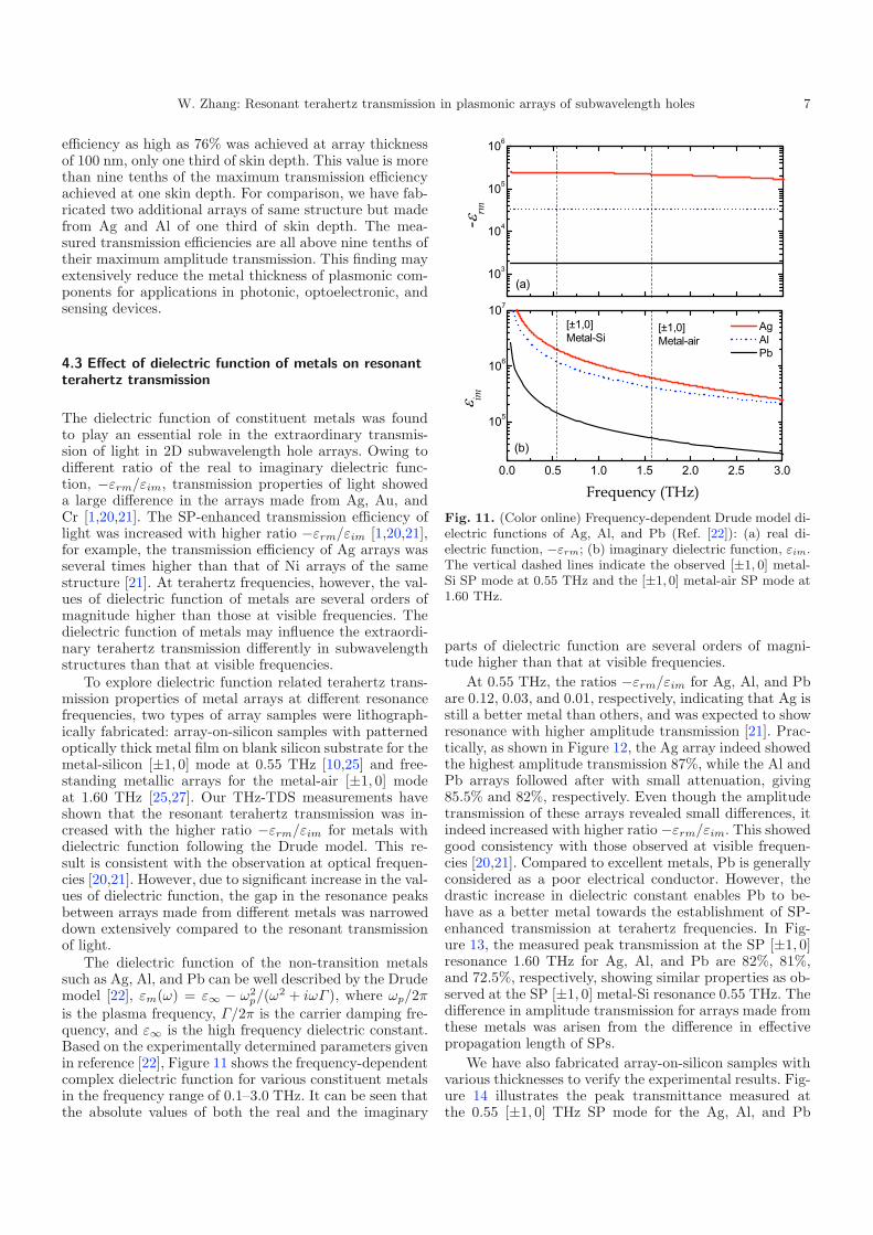
The dielectric function of constituent metals was foundto play an essential role in the extraordinary transmis-sion of light in 2D subwavelength hole arrays. Owing todifferent ratio of the real to imaginary dielectric func-tion, −εrm/εim, transmission properties of light showeda large difference in the arrays made from Ag, Au, andCr [1,20,21]. The SP-enhanced transmission efficiency oflight was increased with higher ratio −εrm/εim [1,20,21],for example, the transmission efficiency of Ag arrays wasseveral times higher than that of Ni arrays of the samestructure [21]. At terahertz frequencies, however, the val-ues of dielectric function of metals are several orders ofmagnitude higher than those at visible frequencies. Thedielectric function of metals may influence the extraordi-nary terahertz transmission differently in subwavelengthstructures than that at visible frequencies.
To explore dielectric function related terahertz trans-mission properties of metal arrays at different resonancefrequencies, two types of array samples were lithograph-ically fabricated: array-on-silicon samples with patternedoptically thick metal film on blank silicon substrate for themetal-silicon [±1, 0] mode at 0.55 THz [10,25] and free-standing metallic arrays for the metal-air [±1, 0] modeat 1.60 THz [25,27]. Our THz-TDS measurements haveshown that the resonant terahertz transmission was in-creased with the higher ratio −εrm/εim for metals withdielectric function following the Drude model. This re-sult is consistent with the observation at optical frequen-cies [20,21]. However, due to significant increase in the val-ues of dielectric function, the gap in the resonance peaksbetween arrays made from different metals was narroweddown extensively compared to the resonant transmissionof light.
The dielectric function of the non-transition metalssuch as Ag, Al, and Pb can be well described by the Drudemodel [22], εm(ω) = ε∞ − ω2
p/(ω2 + iωΓ ), where ωp/2πis the plasma frequency, Γ/2π is the carrier damping fre-quency, and ε∞ is the high frequency dielectric constant.Based on the experimentally determined parameters givenin reference [22], Figure 11 shows the frequency-dependentcomplex dielectric function for various constituent metalsin the frequency range of 0.1–3.0 THz. It can be seen thatthe absolute values of both the real and the imaginary
103
104
105
106
0.0 0.5 1.0 1.5 2.0 2.5 3.0
105
106
107
-rm
(a)
Frequency (THz) im
Ag
Al
Pb
(b)
[±1,0]
Metal-air
[±1,0]
Metal-Si
Fig. 11. (Color online) Frequency-dependent Drude model di-electric functions of Ag, Al, and Pb (Ref. [22]): (a) real di-electric function, −εrm; (b) imaginary dielectric function, εim.The vertical dashed lines indicate the observed [±1, 0] metal-Si SP mode at 0.55 THz and the [±1, 0] metal-air SP mode at1.60 THz.
parts of dielectric function are several orders of magni-tude higher than that at visible frequencies.
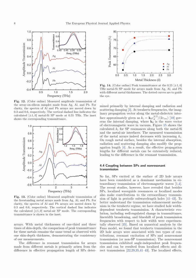
At 0.55 THz, the ratios −εrm/εim for Ag, Al, and Pbare 0.12, 0.03, and 0.01, respectively, indicating that Ag isstill a better metal than others, and was expected to showresonance with higher amplitude transmission [21]. Prac-tically, as shown in Figure 12, the Ag array indeed showedthe highest amplitude transmission 87%, while the Al andPb arrays followed after with small attenuation, giving85.5% and 82%, respectively. Even though the amplitudetransmission of these arrays revealed small differences, itindeed increased with higher ratio −εrm/εim. This showedgood consistency with those observed at visible frequen-cies [20,21]. Compared to excellent metals, Pb is generallyconsidered as a poor electrical conductor. However, thedrastic increase in dielectric constant enables Pb to be-have as a better metal towards the establishment of SP-enhanced transmission at terahertz frequencies. In Fig-ure 13, the measured peak transmission at the SP [±1, 0]resonance 1.60 THz for Ag, Al, and Pb are 82%, 81%,and 72.5%, respectively, showing similar properties as ob-served at the SP [±1, 0] metal-Si resonance 0.55 THz. Thedifference in amplitude transmission for arrays made fromthese metals was arisen from the difference in effectivepropagation length of SPs.
We have also fabricated array-on-silicon samples withvarious thicknesses to verify the experimental results. Fig-ure 14 illustrates the peak transmittance measured atthe 0.55 [±1, 0] THz SP mode for the Ag, Al, and Pb
8 The European Physical Journal Applied Physics
0.5 1.0 1.5 2.0-0.4
-0.2
0.0
0.2
0.4
0.6
0.8
1.0
0.40 0.45 0.50 0.55
0.2
0.4
0.6
Pb
Al
Ag
Am
plitu
de T
rans
mis
sion
Frequency (THz)
Freq. (THz)Tr
ansm
ittan
ce
Fig. 12. (Color online) Measured amplitude transmission ofthe array-on-silicon samples made from Ag, Al, and Pb. Forclarity, the spectra of Al and Pb arrays are moved down by0.3 and 0.6, respectively. The vertical dashed line indicates thecalculated [±1, 0] metal-Si SP mode at 0.55 THz. The insetshows the corresponding transmittance.
1 2 3 4-0.6
-0.4
-0.2
0.0
0.2
0.4
0.6
0.8
1.0
1.2 1.5 1.8
0.2
0.4
0.6
Pb
Al
Ag
Am
plitu
de T
rans
mis
sion
Frequency (THz)
Freq. (THz)
Tran
smitt
ance
Fig. 13. (Color online) Measured amplitude transmission ofthe freestanding metal arrays made from Ag, Al, and Pb. Forclarity, the spectra of Al and Pb arrays are moved down by0.3 and 0.6, respectively. The vertical dashed line indicatesthe calculated [±1, 0] metal-air SP mode. The correspondingtransmittance is shown in the inset.
arrays. With metal thicknesses of one-third and threetimes of skin-depth, the comparison of peak transmittancefor these metals remains the same trend as observed withone skin-depth thickness, demonstrating the consistencyof our measurements.
The difference in resonant transmission for arraysmade from different metals is primarily arisen from thedifference in effective propagation length of SPs deter-
0.0 0.5 1.0 1.5 2.0 2.5 3.0
60
65
70
75
80
Ag Al Pb
Peak
Tra
nsm
ittan
ce (%
)
Metal Thickness (δ)
Fig. 14. (Color online) Peak transmittance at the 0.55 [±1, 0]THz metal-Si SP mode for arrays made from Ag, Al, and Pbwith different metal thicknesses. The dotted curves are to guidethe eye.
mined primarily by internal damping and radiation andscattering damping [3]. At terahertz frequencies, the imag-inary propagation vector along the metal-dielectric inter-face approximately given as ki = k0ε
3/2d /(2εim) [10] gov-
erns the internal damping, where k0 is the wave vectorof electromagnetic wave in vacuum. Figure 15 shows thecalculated ki for SP resonances along both the metal-Siand the metal-air interfaces. The measured transmissionof the metal arrays indeed decreases with increasing ki.On rough metal surface, besides the internal absorption,radiation and scattering damping also modify the prop-agation length [4]. As a result, the effective propagationlengths for different metals can be extensively reduced,leading to the difference in the resonant transmission.
4.4 Coupling between SPs and nonresonanttransmission
So far, SPs excited at the surface of 2D hole arrayshave been considered as a dominant mechanism in ex-traordinary transmission of electromagnetic waves [1,4].The recent studies, however, have revealed that besidesSPs, localized waveguide resonances or localized modesalso make contributions to the extraordinary transmis-sion of light in periodic subwavelength holes [41–43]. Tobetter understand the transmission enhancement mecha-nism in the terahertz regime, we have studied hole width-dependent terahertz transmission. A characteristic evo-lution, including well-regulated change in transmittance,linewidth broadening, and blueshift of peak transmissionfrequencies with respect to hole width were experimen-tally observed [35]. Based on numerical analysis by theFano model, we found that terahertz transmission in the2D hole arrays were associated with two types of con-tributions, resonant excitation of SPs and nonresonanttransmission (or non-SP transmission). The nonresonanttransmission exhibited angle-independent peak frequen-cies and can be resulted from localized effects and di-rect transmission [22,29,35,41–43]. The localized effects,
W. Zhang: Resonant terahertz transmission in plasmonic arrays of subwavelength holes 9
10-2
10-1
100
101
102
(a)
ki(m
-1)
[±1,0]
Metal-silicon
Ag
Al
Pb
0 1 2 3
10-4
10-3
10-2
10-1
100
(b)
ki(m
-1)
[±1,0]
Metal-air
Frequency (THz)
Fig. 15. (Color online) Calculated imaginary propagation vec-tors of SPs for Ag, Al, and Pb along (a) metal-Si interface and(b) metal-air interfaces.
as either localized modes or localized waveguide reso-nances [41–43], also contributed substantially to enhancedterahertz transmission. The direct transmission, on theother hand, due to scattering and low filling fraction ofmetal, was the origin that causes the reduction in trans-mission efficiency of the holes.
In sample preparation, a set of 2D hexagonal arraysof rectangular subwavelength holes are lithographicallyfabricated with a 180-nm-thick Al film onto a siliconsubstrate [35]. Each sample, with dimensions of 15 ×15 mm2, has holes of a fixed length 120 μm and var-ious widths from 40 to 140 μm with a 20-μm inter-val, and a constant periodicity of 160 μm. Figure 16 il-lustrates the frequency-dependent absolute transmittanceand the corresponding phase change for an array withhole dimensions of 120 × 40 μm2. At normal incidence,the resonant frequency can be approximately given byequation (3) with the grating momentum wave vector,Gmn = 4π(m2 + n2 + mn)1/2/
√3L for the 2D hexago-
nal hole arrays. The calculated fundamental SP [±1, 0]resonance of hexagonal arrays at the Al-Si interface wasaround 0.63 THz, which was higher than the measuredtransmission peak 0.49 THz due to the fact that the latterwas a result of both resonant and nonresonant contribu-tions [10,12,44].
0.4 0.8 1.2 1.6 2.00.0
0.2
0.4
0.6
0.8
1.0
0.4 0.8 1.2 1.6 2.0
-2
0
2
Tran
smitt
ance
Frequency (THz)
Frequency (THz)
Phas
e (r
ad)
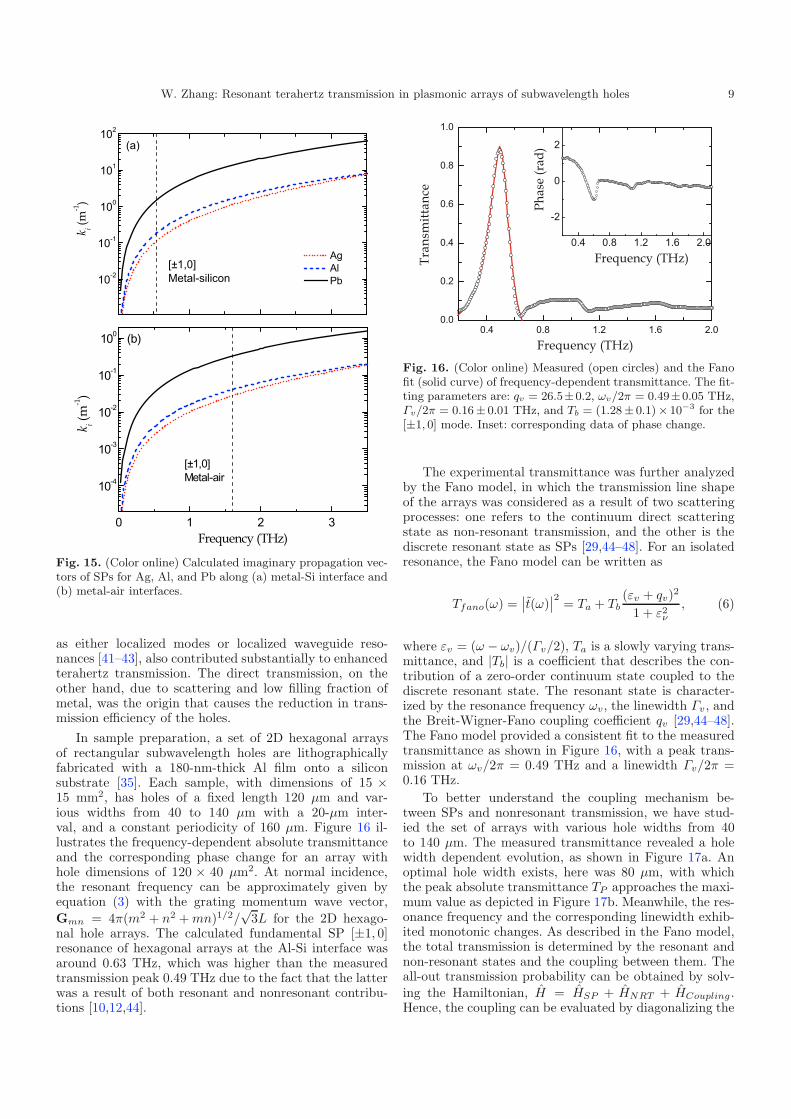
Fig. 16. (Color online) Measured (open circles) and the Fanofit (solid curve) of frequency-dependent transmittance. The fit-ting parameters are: qv = 26.5±0.2, ωv/2π = 0.49±0.05 THz,Γv/2π = 0.16± 0.01 THz, and Tb = (1.28± 0.1)× 10−3 for the[±1, 0] mode. Inset: corresponding data of phase change.
The experimental transmittance was further analyzedby the Fano model, in which the transmission line shapeof the arrays was considered as a result of two scatteringprocesses: one refers to the continuum direct scatteringstate as non-resonant transmission, and the other is thediscrete resonant state as SPs [29,44–48]. For an isolatedresonance, the Fano model can be written as
Tfano(ω) =∣∣t(ω)
∣∣2 = Ta + Tb(εv + qv)2
1 + ε2ν
, (6)
where εv = (ω − ωv)/(Γv/2), Ta is a slowly varying trans-mittance, and |Tb| is a coefficient that describes the con-tribution of a zero-order continuum state coupled to thediscrete resonant state. The resonant state is character-ized by the resonance frequency ωv, the linewidth Γv, andthe Breit-Wigner-Fano coupling coefficient qv [29,44–48].The Fano model provided a consistent fit to the measuredtransmittance as shown in Figure 16, with a peak trans-mission at ωv/2π = 0.49 THz and a linewidth Γv/2π =0.16 THz.
To better understand the coupling mechanism be-tween SPs and nonresonant transmission, we have stud-ied the set of arrays with various hole widths from 40to 140 μm. The measured transmittance revealed a holewidth dependent evolution, as shown in Figure 17a. Anoptimal hole width exists, here was 80 μm, with whichthe peak absolute transmittance TP approaches the maxi-mum value as depicted in Figure 17b. Meanwhile, the res-onance frequency and the corresponding linewidth exhib-ited monotonic changes. As described in the Fano model,the total transmission is determined by the resonant andnon-resonant states and the coupling between them. Theall-out transmission probability can be obtained by solv-ing the Hamiltonian, H = HSP + HNRT + HCoupling .Hence, the coupling can be evaluated by diagonalizing the
10 The European Physical Journal Applied Physics
2
4
6
0.5 1.0 1.5 2.0 2.50
1
2
3(a)
120 x 40 m2
120 x 60 m2
120 x 80 m2
120 x 100 m2
120 x 120 m2
Tra
nsm
itta
nce
Frequency (THz)
120 x 140 m2
40 60 80 100 120 1400.7
0.8
0.9
1.0
TP
(b)
Hole width ( m)
TN
Fig. 17. (Color online) (a) Measured frequency dependent ab-solute transmittance of the hole arrays with fixed hole lengthof 120 μm and various hole widths from 40 to 140 μm withan interval of 20 μm. For clarity, the curves are vertically dis-placed by 0.36. (b) Absolute (squares) and normalized (circles)peak transmittance as a function of hole width.
Hamiltonian matrix [17,35,44,45],
H = �
⎛⎝ωSP χ
χ∗ ωNRT
⎞⎠ , (7)
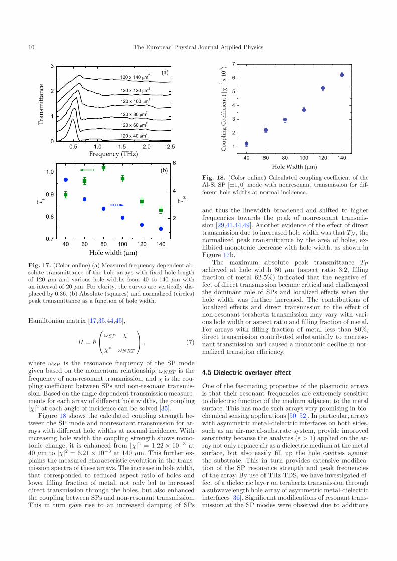
where ωSP is the resonance frequency of the SP modegiven based on the momentum relationship, ωNRT is thefrequency of non-resonant transmission, and χ is the cou-pling coefficient between SPs and non-resonant transmis-sion. Based on the angle-dependent transmission measure-ments for each array of different hole widths, the coupling|χ|2 at each angle of incidence can be solved [35].
Figure 18 shows the calculated coupling strength be-tween the SP mode and nonresonant transmission for ar-rays with different hole widths at normal incidence. Withincreasing hole width the coupling strength shows mono-tonic change; it is enhanced from |χ|2 = 1.22 × 10⁻³ at40 μm to |χ|2 = 6.21 × 10⁻³ at 140 μm. This further ex-plains the measured characteristic evolution in the trans-mission spectra of these arrays. The increase in hole width,that corresponded to reduced aspect ratio of holes andlower filling fraction of metal, not only led to increaseddirect transmission through the holes, but also enhancedthe coupling between SPs and non-resonant transmission.This in turn gave rise to an increased damping of SPs
40 60 80 100 120 140
1
2
3
4
5
6
7
Hole Width (μm)
Cou
plin
g C
oeff
icie
nt (|
χ|2 x
10-3
)
Fig. 18. (Color online) Calculated coupling coefficient of theAl-Si SP [±1, 0] mode with nonresonant transmission for dif-ferent hole widths at normal incidence.
and thus the linewidth broadened and shifted to higherfrequencies towards the peak of nonresonant transmis-sion [29,41,44,49]. Another evidence of the effect of directtransmission due to increased hole width was that TN , thenormalized peak transmittance by the area of holes, ex-hibited monotonic decrease with hole width, as shown inFigure 17b.
The maximum absolute peak transmittance TP
achieved at hole width 80 μm (aspect ratio 3:2, fillingfraction of metal 62.5%) indicated that the negative ef-fect of direct transmission became critical and challengeedthe dominant role of SPs and localized effects when thehole width was further increased. The contributions oflocalized effects and direct transmission to the effect ofnon-resonant terahertz transmission may vary with vari-ous hole width or aspect ratio and filling fraction of metal.For arrays with filling fraction of metal less than 80%,direct transmission contributed substantially to nonreso-nant transmission and caused a monotonic decline in nor-malized transition efficiency.
4.5 Dielectric overlayer effect
One of the fascinating properties of the plasmonic arraysis that their resonant frequencies are extremely sensitiveto dielectric function of the medium adjacent to the metalsurface. This has made such arrays very promising in bio-chemical sensing applications [50–52]. In particular, arrayswith asymmetric metal-dielectric interfaces on both sides,such as an air-metal-substrate system, provide improvedsensitivity because the analytes (ε > 1) applied on the ar-ray not only replace air as a dielectric medium at the metalsurface, but also easily fill up the hole cavities againstthe substrate. This in turn provides extensive modifica-tion of the SP resonance strength and peak frequenciesof the array. By use of THz-TDS, we have investigated ef-fect of a dielectric layer on terahertz transmission througha subwavelength hole array of asymmetric metal-dielectricinterfaces [36]. Significant modifications of resonant trans-mission at the SP modes were observed due to additions
W. Zhang: Resonant terahertz transmission in plasmonic arrays of subwavelength holes 11
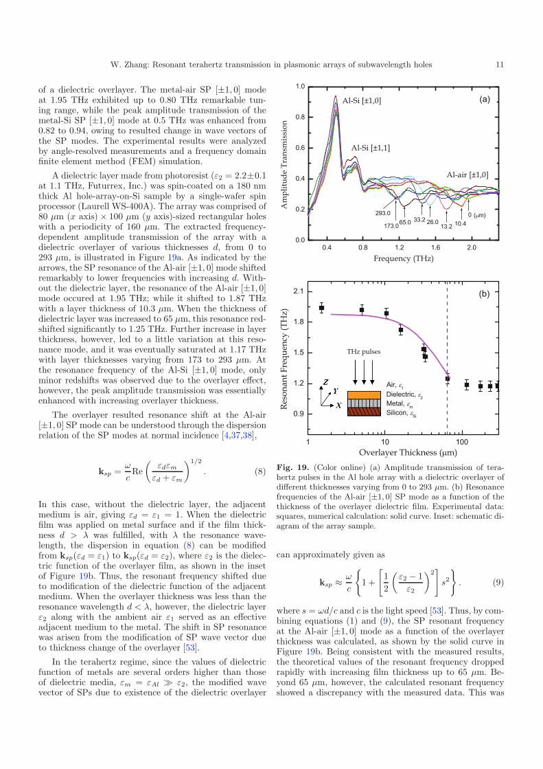
of a dielectric overlayer. The metal-air SP [±1, 0] modeat 1.95 THz exhibited up to 0.80 THz remarkable tun-ing range, while the peak amplitude transmission of themetal-Si SP [±1, 0] mode at 0.5 THz was enhanced from0.82 to 0.94, owing to resulted change in wave vectors ofthe SP modes. The experimental results were analyzedby angle-resolved measurements and a frequency domainfinite element method (FEM) simulation.
A dielectric layer made from photoresist (ε2 = 2.2±0.1at 1.1 THz, Futurrex, Inc.) was spin-coated on a 180 nmthick Al hole-array-on-Si sample by a single-wafer spinprocessor (Laurell WS-400A). The array was comprised of80 μm (x axis) × 100 μm (y axis)-sized rectangular holeswith a periodicity of 160 μm. The extracted frequency-dependent amplitude transmission of the array with adielectric overlayer of various thicknesses d, from 0 to293 μm, is illustrated in Figure 19a. As indicated by thearrows, the SP resonance of the Al-air [±1, 0] mode shiftedremarkably to lower frequencies with increasing d. With-out the dielectric layer, the resonance of the Al-air [±1, 0]mode occured at 1.95 THz; while it shifted to 1.87 THzwith a layer thickness of 10.3 μm. When the thickness ofdielectric layer was increased to 65 μm, this resonance red-shifted significantly to 1.25 THz. Further increase in layerthickness, however, led to a little variation at this reso-nance mode, and it was eventually saturated at 1.17 THzwith layer thicknesses varying from 173 to 293 μm. Atthe resonance frequency of the Al-Si [±1, 0] mode, onlyminor redshifts was observed due to the overlayer effect,however, the peak amplitude transmission was essentiallyenhanced with increasing overlayer thickness.
The overlayer resulted resonance shift at the Al-air[±1, 0] SP mode can be understood through the dispersionrelation of the SP modes at normal incidence [4,37,38],
ksp =ω
cRe
(εdεm
εd + εm
)1/2
. (8)
In this case, without the dielectric layer, the adjacentmedium is air, giving εd = ε1 = 1. When the dielectricfilm was applied on metal surface and if the film thick-ness d > λ was fulfilled, with λ the resonance wave-length, the dispersion in equation (8) can be modifiedfrom ksp(εd = ε1) to ksp(εd = ε2), where ε2 is the dielec-tric function of the overlayer film, as shown in the insetof Figure 19b. Thus, the resonant frequency shifted dueto modification of the dielectric function of the adjacentmedium. When the overlayer thickness was less than theresonance wavelength d < λ, however, the dielectric layerε2 along with the ambient air ε1 served as an effectiveadjacent medium to the metal. The shift in SP resonancewas arisen from the modification of SP wave vector dueto thickness change of the overlayer [53].
In the terahertz regime, since the values of dielectricfunction of metals are several orders higher than thoseof dielectric media, εm = εAl � ε2, the modified wavevector of SPs due to existence of the dielectric overlayer
Fig. 19. (Color online) (a) Amplitude transmission of tera-hertz pulses in the Al hole array with a dielectric overlayer ofdifferent thicknesses varying from 0 to 293 μm. (b) Resonancefrequencies of the Al-air [±1, 0] SP mode as a function of thethickness of the overlayer dielectric film. Experimental data:squares, numerical calculation: solid curve. Inset: schematic di-agram of the array sample.
can approximately given as
ksp ≈ ω
c
{1 +
[12
(ε2 − 1
ε2
)2]
s2
}. (9)
where s = ωd/c and c is the light speed [53]. Thus, by com-bining equations (1) and (9), the SP resonant frequencyat the Al-air [±1, 0] mode as a function of the overlayerthickness was calculated, as shown by the solid curve inFigure 19b. Being consistent with the measured results,the theoretical values of the resonant frequency droppedrapidly with increasing film thickness up to 65 μm. Be-yond 65 μm, however, the calculated resonant frequencyshowed a discrepancy with the measured data. This was
12 The European Physical Journal Applied Physics
(a) (b)
(c) (d)
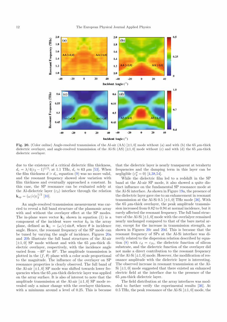
Fig. 20. (Color online) Angle-resolved transmission of the Al-air (AA) [±1, 0] mode without (a) and with (b) the 65 μm-thickdielectric overlayer, and angle-resolved transmission of the Al-Si (AS) [±1, 0] mode without (c) and with (d) the 65 μm-thickdielectric overlayer.
due to the existence of a critical dielectric film thickness,dc = λ/4(ε2 − 1)1/2; at 1.1 THz, dc ≈ 63 μm [53]. Whenthe film thickness d > dc, equation (9) was no more valid,and the resonant frequency showed slow variation withfilm thickness and eventually approached a constant. Inthis case, the SP resonance can be evaluated solely atthe Al-dielectric layer (ε2) interface through the relationksp = (ω/c)ε1/2
2 [10].
An angle-resolved transmission measurement was car-ried to reveal a full band structure of the plasmonic arraywith and without the overlayer effect at the SP modes.The in-plane wave vector k|| shown in equation (1) is acomponent of the incident wave vector k0 in the arrayplane, defined as k|| = (ω/c) sin θ, where θ is incidenceangle. Hence, the resonant frequency of the SP mode canbe tuned by varying the angle of incidence. Figures 20aand 20b illustrate the full band structures of the Al-air[±1, 0] SP mode without and with the 65 μm-thick di-electric overlayer, respectively, with the incidence anglevaried from −40◦ to 40◦. The amplitude transmission isplotted in the (f , θ) plane with a color scale proportionalto the magnitude. The influence of the overlayer on SPresonance properties is clearly observed. The full band ofthe Al-air [±1, 0] SP mode was shifted towards lower fre-quencies when the 65 μm-thick dielectric layer was appliedon the array surface. It is also of interest to note that theamplitude transmission at the Al-air [±1, 0] SP mode re-vealed only a minor change with the overlayer thickness,with a minimum around a level of 0.25. This is because
that the dielectric layer is nearly transparent at terahertzfrequencies and the damping term in this layer can benegligible (ε′′2 = 0) [4,38,54].
While the dielectric film led to a redshift in the SPband at the Al-air SP mode, it also showed a quite dis-tinct influence on the fundamental SP resonance mode atthe Al-Si interface. As shown in Figure 19a, the presence ofthe dielectric layer gave rise to an enhancement in resonanttransmission at the Al-Si 0.5 [±1, 0] THz mode [36]. Withthe 65 μm-thick overlayer, the peak amplitude transmis-sion increased from 0.82 to 0.94 at normal incidence, but itrarely affected the resonant frequency. The full band struc-ture of the Al-Si [±1, 0] mode with the overlalyer remainednearly unchanged compared to that of the bare metal ar-ray, except for the increase in transmission strength, asshown in Figures 20c and 20d. This is because that theresonant frequency of SPs at the Al-Si interface was di-rectly related to the dispersion relation described by equa-tion (8) with εd = εSi, the dielectric function of siliconsubstrate, and the dielectric function of the overlayer didnot make a direct contribution to the resonant frequencyof the Al-Si [±1, 0] mode. However, the modification of res-onance amplitude with the dielectric layer is interesting.The observed increase in resonant transmission at the Al-Si [±1, 0] mode suggested that there existed an enhancedelectric field at the interface due to the presence of the65 μm-thick dielectric layer.
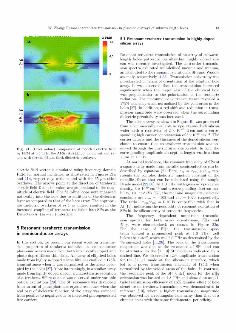
The field distribution at the array interfaces was mod-eled to further verify the experimental results [36]. At0.5 THz, the peak resonance of the Al-Si [±1, 0] mode, the
W. Zhang: Resonant terahertz transmission in plasmonic arrays of subwavelength holes 13
Fig. 21. (Color online) Comparison of modeled electric fieldby FEM at 0.5 THz, the Al-Si (AS) [±1, 0] mode, without (a)and with (b) the 65 μm-thick dielectric overlayer.
electric field vector is simulated using frequency domainFEM for normal incidence, as illustrated in Figures 21aand 21b, respectively, without and with the 65 μm-thickoverlayer. The arrows point at the direction of terahertzelectric field E and the colors are proportional to the mag-nitude of electric field. The field-line loops were enhancednoticeably into the hole due to addition of the dielectriclayer as compared to that of the bare array. The appropri-ate dielectric overlayer of ε2 > ε1 indeed resulted in theincreased coupling of terahertz radiation into SPs at theDielectric-Al (ε2 − εm) interface.
5 Resonant terahertz transmissionin semiconductor arrays
In this section, we present our recent work on transmis-sion properties of terahertz radiation in semiconductorplasmonic arrays made from both intrinsically doped andphoto-doped silicon thin slabs. An array of elliptical holesmade from highly n-doped silicon film has enabled a 175%transmittance when it was normalized to the areas occu-pied by the holes [27]. More interestingly, in a similar arraymade from lightly doped silicon, a characteristic evolutionof a terahertz SP resonance was observed under variableoptical excitations [29]. The SP resonance was developedfrom an out-of-plane photonics crystal resonance when thereal part of dielectric function of the array was switchedfrom positive to negative due to increased photogeneratedfree carriers.
5.1 Resonant terahertz transmission in highly-dopedsilicon arrays
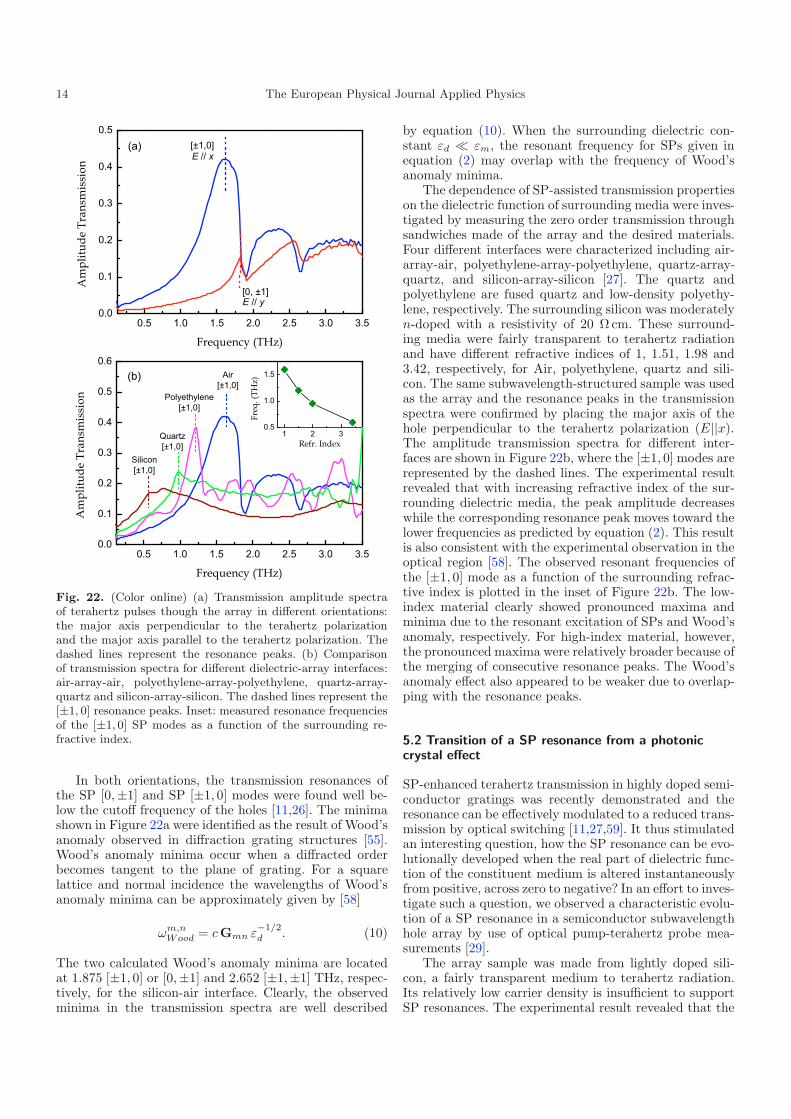
Resonant terahertz transmission of an array of subwave-length holes patterned on ultrathin, highly doped sili-con was recently investigated. The zero-order transmis-sion spectra exhibited well-defined maxima and minima,as attributed to the resonant excitation of SPs and Wood’sanomaly, respectively [4,55]. Transmission anisotropy wasinvestigated in terms of orientation of the elliptical holearray. It was observed that the transmission increasedsignificantly when the major axis of the elliptical holewas perpendicular to the polarization of the terahertzradiation. The measured peak transmittance revealed a175% efficiency when normalized by the void areas in theholes [27]. In addition, a red-shift and reduction in trans-mission amplitude were observed when the surroundingdielectric permittivity was increased.
The silicon array, as shown in Figure 4b, was processedfrom a commercially available n-type, 50-μm-thick siliconwafer with a resistivity of 2 × 10⁻³ Ω cm and a corre-sponding high carrier concentration of 3×1019 cm−3. Thecarrier density and the thickness of the doped silicon werechosen to ensure that no terahertz transmission was ob-served through the unstructured silicon slab. In fact, thecorresponding amplitude absorption length was less than1 μm at 1 THz.
At normal incidence, the resonant frequency of SPs ofa square array made from metallic semiconductors can bedescribed by equation (2). Here, εm = εrm + iεim rep-resents the complex dielectric function constant of themetallic silicon that can be calculated using the simpleDrude model [22,56]. At 1.0 THz, with given n-type carrierdensity, 3 × 1019 cm−3 and a corresponding electron mo-bility, 120 cm2/Vs [57], the real and imaginary dielectricconstants are εrm = −103 and εim = 1020, respectively.The ratio −εrm/εim = 0.10 is compatible with that inAl [10], indicating the possibility of resonant excitation ofSPs in the silicon array at terahertz frequencies.
The frequency dependent amplitude transmis-sion spectra for both array orientations, E||x andE||y, were characterized, as shown in Figure 22a.For the case of E||x, the transmission spec-trum showed a pronounced peak at 1.6 THz, wellbelow the cutoff, which was 2.0 THz as determined by the75-μm-sized holes [11,26]. The peak of the transmissionmagnitude was due to the resonance of SPs and canbe attributed to the [±1, 0] SP mode as indicated by adashed line. We observed a 42% amplitude transmissionfor the [±1, 0] mode at the silicon-air interface, whichled to a power transmission efficiency of 175% whennormalized by the voided areas of the holes. In contrast,the resonance peak of the SP [0,±1] mode for the E||yorientation was located at 1.8 THz and showed an ampli-tude transmission efficiency of 16%. Similar effect of holestructure on terahertz transmission was demonstrated inreference [10], where a higher transmission magnitudewas observed for a rectangular hole array than that of acircular holes with the same fundamental periodicity.
14 The European Physical Journal Applied Physics
0.5 1.0 1.5 2.0 2.5 3.0 3.50.0
0.1
0.2
0.3
0.4
0.5
(a)
[0, ±1]E // y
E // x[±1,0]
Am
pli
tud
e T
ran
smis
sio
n
Frequency (THz)
0.5 1.0 1.5 2.0 2.5 3.0 3.50.0
0.1
0.2
0.3
0.4
0.5
0.6
1 2 30.5
1.0
1.5(b)
Silicon
[±1,0]
Quartz
[±1,0]
Polyethylene
[±1,0]
Air
[±1,0]
Am
pli
tud
e T
ran
smis
sio
n
Frequency (THz)
Fre
q. (
TH
z)
Refr. Index
Fig. 22. (Color online) (a) Transmission amplitude spectraof terahertz pulses though the array in different orientations:the major axis perpendicular to the terahertz polarizationand the major axis parallel to the terahertz polarization. Thedashed lines represent the resonance peaks. (b) Comparisonof transmission spectra for different dielectric-array interfaces:air-array-air, polyethylene-array-polyethylene, quartz-array-quartz and silicon-array-silicon. The dashed lines represent the[±1, 0] resonance peaks. Inset: measured resonance frequenciesof the [±1, 0] SP modes as a function of the surrounding re-fractive index.
In both orientations, the transmission resonances ofthe SP [0,±1] and SP [±1, 0] modes were found well be-low the cutoff frequency of the holes [11,26]. The minimashown in Figure 22a were identified as the result of Wood’sanomaly observed in diffraction grating structures [55].Wood’s anomaly minima occur when a diffracted orderbecomes tangent to the plane of grating. For a squarelattice and normal incidence the wavelengths of Wood’sanomaly minima can be approximately given by [58]
ωm,nWood = cGmn ε
−1/2d . (10)
The two calculated Wood’s anomaly minima are locatedat 1.875 [±1, 0] or [0,±1] and 2.652 [±1,±1] THz, respec-tively, for the silicon-air interface. Clearly, the observedminima in the transmission spectra are well described
by equation (10). When the surrounding dielectric con-stant εd � εm, the resonant frequency for SPs given inequation (2) may overlap with the frequency of Wood’sanomaly minima.
The dependence of SP-assisted transmission propertieson the dielectric function of surrounding media were inves-tigated by measuring the zero order transmission throughsandwiches made of the array and the desired materials.Four different interfaces were characterized including air-array-air, polyethylene-array-polyethylene, quartz-array-quartz, and silicon-array-silicon [27]. The quartz andpolyethylene are fused quartz and low-density polyethy-lene, respectively. The surrounding silicon was moderatelyn-doped with a resistivity of 20 Ω cm. These surround-ing media were fairly transparent to terahertz radiationand have different refractive indices of 1, 1.51, 1.98 and3.42, respectively, for Air, polyethylene, quartz and sili-con. The same subwavelength-structured sample was usedas the array and the resonance peaks in the transmissionspectra were confirmed by placing the major axis of thehole perpendicular to the terahertz polarization (E||x).The amplitude transmission spectra for different inter-faces are shown in Figure 22b, where the [±1, 0] modes arerepresented by the dashed lines. The experimental resultrevealed that with increasing refractive index of the sur-rounding dielectric media, the peak amplitude decreaseswhile the corresponding resonance peak moves toward thelower frequencies as predicted by equation (2). This resultis also consistent with the experimental observation in theoptical region [58]. The observed resonant frequencies ofthe [±1, 0] mode as a function of the surrounding refrac-tive index is plotted in the inset of Figure 22b. The low-index material clearly showed pronounced maxima andminima due to the resonant excitation of SPs and Wood’sanomaly, respectively. For high-index material, however,the pronounced maxima were relatively broader because ofthe merging of consecutive resonance peaks. The Wood’sanomaly effect also appeared to be weaker due to overlap-ping with the resonance peaks.
5.2 Transition of a SP resonance from a photoniccrystal effect
SP-enhanced terahertz transmission in highly doped semi-conductor gratings was recently demonstrated and theresonance can be effectively modulated to a reduced trans-mission by optical switching [11,27,59]. It thus stimulatedan interesting question, how the SP resonance can be evo-lutionally developed when the real part of dielectric func-tion of the constituent medium is altered instantaneouslyfrom positive, across zero to negative? In an effort to inves-tigate such a question, we observed a characteristic evolu-tion of a SP resonance in a semiconductor subwavelengthhole array by use of optical pump-terahertz probe mea-surements [29].
The array sample was made from lightly doped sili-con, a fairly transparent medium to terahertz radiation.Its relatively low carrier density is insufficient to supportSP resonances. The experimental result revealed that the
W. Zhang: Resonant terahertz transmission in plasmonic arrays of subwavelength holes 15
Air Reference
(a) (b)
Blank Silicon
Am
plitu
de (a
.u.)
PerpendicularArray
Am
pitu
de (a
.u.)
2 4 6 8 10
ParallelArray
Delay (ps)0.5 1.0 1.5 2.0 2.5
Frequency (THz)
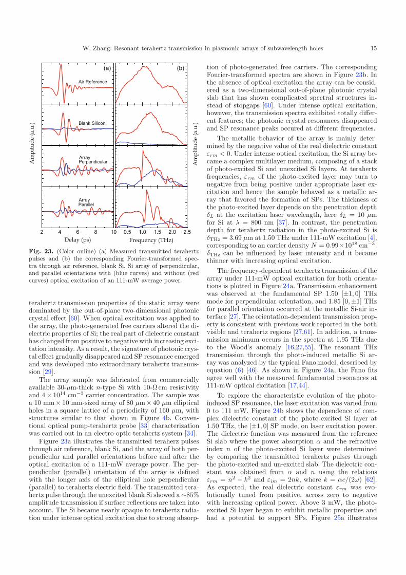
Fig. 23. (Color online) (a) Measured transmitted terahertzpulses and (b) the corresponding Fourier-transformed spec-tra through air reference, blank Si, Si array of perpendicular,and parallel orientations with (blue curves) and without (redcurves) optical excitation of an 111-mW average power.
terahertz transmission properties of the static array weredominated by the out-of-plane two-dimensional photoniccrystal effect [60]. When optical excitation was applied tothe array, the photo-generated free carriers altered the di-electric properties of Si; the real part of dielectric constanthas changed from positive to negative with increasing exci-tation intensity. As a result, the signature of photonic crys-tal effect gradually disappeared and SP resonance emergedand was developed into extraordinary terahertz transmis-sion [29].
The array sample was fabricated from commerciallyavailable 30-μm-thick n-type Si with 10-Ωcm resistivityand 4× 1014 cm−3 carrier concentration. The sample wasa 10 mm× 10 mm-sized array of 80 μm× 40 μm ellipticalholes in a square lattice of a periodicity of 160 μm, withstructures similar to that shown in Figure 4b. Conven-tional optical pump-terahertz probe [33] characterizationwas carried out in an electro-optic terahertz system [34].
Figure 23a illustrates the transmitted teraherz pulsesthrough air reference, blank Si, and the array of both per-pendicular and parallel orientations before and after theoptical excitation of a 111-mW average power. The per-pendicular (parallel) orientation of the array is definedwith the longer axis of the elliptical hole perpendicular(parallel) to terahertz electric field. The transmitted tera-hertz pulse through the unexcited blank Si showed a ∼85%amplitude transmission if surface reflections are taken intoaccount. The Si became nearly opaque to terahertz radia-tion under intense optical excitation due to strong absorp-
tion of photo-generated free carriers. The correspondingFourier-transformed spectra are shown in Figure 23b. Inthe absence of optical excitation the array can be consid-ered as a two-dimensional out-of-plane photonic crystalslab that has shown complicated spectral structures in-stead of stopgaps [60]. Under intense optical excitation,however, the transmission spectra exhibited totally differ-ent features; the photonic crystal resonances disappearedand SP resonance peaks occured at different frequencies.
The metallic behavior of the array is mainly deter-mined by the negative value of the real dielectric constantεrm < 0. Under intense optical excitation, the Si array be-came a complex multilayer medium, composing of a stackof photo-excited Si and unexcited Si layers. At terahertzfrequencies, εrm of the photo-excited layer may turn tonegative from being positive under appropriate laser ex-citation and hence the sample behaved as a metallic ar-ray that favored the formation of SPs. The thickness ofthe photo-excited layer depends on the penetration depthδL at the excitation laser wavelength, here δL = 10 μmfor Si at λ = 800 nm [37]. In contrast, the penetrationdepth for terahertz radiation in the photo-excited Si isδTHz = 3.69 μm at 1.50 THz under 111-mW excitation [4],corresponding to an carrier density N = 0.99×1018 cm−3.δTHz can be influenced by laser intensity and it becamethinner with increasing optical excitation.
The frequency-dependent terahertz transmission of thearray under 111-mW optical excitation for both orienta-tions is plotted in Figure 24a. Transmission enhancementwas observed at the fundamental SP 1.50 [±1, 0] THzmode for perpendicular orientation, and 1.85 [0,±1] THzfor parallel orientation occurred at the metallic Si-air in-terface [27]. The orientation-dependent transmission prop-erty is consistent with previous work reported in the bothvisible and terahertz regions [27,61]. In addition, a trans-mission minimum occurs in the spectra at 1.95 THz dueto the Wood’s anomaly [16,27,55]. The resonant THztransmission through the photo-induced metallic Si ar-ray was analyzed by the typical Fano model, described byequation (6) [46]. As shown in Figure 24a, the Fano fitsagree well with the measured fundamental resonances at111-mW optical excitation [17,44].
To explore the characteristic evolution of the photo-induced SP resonance, the laser excitation was varied from0 to 111 mW. Figure 24b shows the dependence of com-plex dielectric constant of the photo-excited Si layer at1.50 THz, the [±1, 0] SP mode, on laser excitation power.The dielectric function was measured from the referenceSi slab where the power absorption α and the refractiveindex n of the photo-excited Si layer were determinedby comparing the transmitted terahertz pulses throughthe photo-excited and un-excited slab. The dielectric con-stant was obtained from α and n using the relationsεrm = n2 − k2 and εim = 2nk, where k = αc/(2ω) [62].As expected, the real dielectric constant εrm was evo-lutionally tuned from positive, across zero to negativewith increasing optical power. Above 3 mW, the photo-excited Si layer began to exhibit metallic properties andhad a potential to support SPs. Figure 25a illustrates
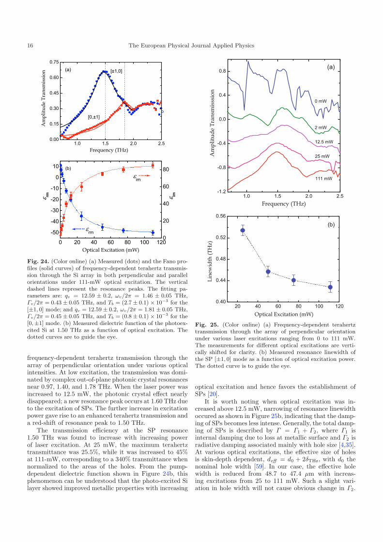
16 The European Physical Journal Applied Physics
1.0 1.5 2.0 2.50.00
0.15
0.30
0.45
0.60
0.75
[0,±1]
[±1,0](a)
Am
pli
tud
e T
ran
smis
sio
n
Frequency (THz)
0 20 40 60 80 100 120
-50
-40
-30
-20
-10
0
10
0
20
40
60
80
rm
im
rm
Optical Excitation (mW)
(b)im
Fig. 24. (Color online) (a) Measured (dots) and the Fano pro-files (solid curves) of frequency-dependent terahertz transmis-sion through the Si array in both perpendicular and parallelorientations under 111-mW optical excitation. The verticaldashed lines represent the resonance peaks. The fitting pa-rameters are: qv = 12.59 ± 0.2, ωv/2π = 1.46 ± 0.05 THz,Γv/2π = 0.43 ± 0.05 THz, and Tb = (2.7 ± 0.1) × 10−3 for the[±1, 0] mode; and qv = 12.59 ± 0.2, ωv/2π = 1.81 ± 0.05 THz,Γv/2π = 0.45 ± 0.05 THz, and Tb = (0.8 ± 0.1) × 10−3 for the[0,±1] mode. (b) Measured dielectric function of the photoex-cited Si at 1.50 THz as a function of optical excitation. Thedotted curves are to guide the eye.
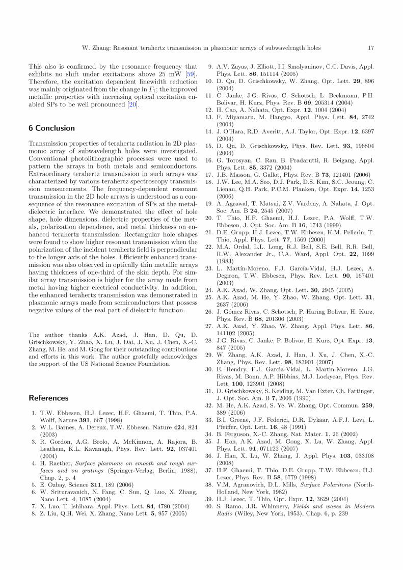
frequency-dependent terahertz transmission through thearray of perpendicular orientation under various opticalintensities. At low excitation, the transmission was domi-nated by complex out-of-plane photonic crystal resonancesnear 0.97, 1.40, and 1.78 THz. When the laser power wasincreased to 12.5 mW, the photonic crystal effect nearlydisappeared; a new resonance peak occurs at 1.60 THz dueto the excitation of SPs. The further increase in excitationpower gave rise to an enhanced terahertz transmission anda red-shift of resonance peak to 1.50 THz.
The transmission efficiency at the SP resonance1.50 THz was found to increase with increasing powerof laser excitation. At 25 mW, the maximum terahertztransmittance was 25.5%, while it was increased to 45%at 111-mW, corresponding to a 340% transmittance whennormalized to the areas of the holes. From the pump-dependent dielectric function shown in Figure 24b, thisphenomenon can be understood that the photo-excited Silayer showed improved metallic properties with increasing
1.0 1.5 2.0 2.5-1.2
-0.8
-0.4
0.0
0.4
0.8
111 mW
25 mW
12.5 mW
2 mW
0 mW
(a)
Am
plitu
de T
rans
mis
ssio
nFrequency (THz)
20 40 60 80 100 1200.40
0.44
0.48
0.52
0.56
(b)
Line
wid
th (T
Hz)
Optical Excitation (mW)
Fig. 25. (Color online) (a) Frequency-dependent terahertztransmission through the array of perpendicular orientationunder various laser excitations ranging from 0 to 111 mW.The measurements for different optical excitations are verti-cally shifted for clarity. (b) Measured resonance linewidth ofthe SP [±1, 0] mode as a function of optical excitation power.The dotted curve is to guide the eye.
optical excitation and hence favors the establishment ofSPs [20].
It is worth noting when optical excitation was in-creased above 12.5 mW, narrowing of resonance linewidthoccured as shown in Figure 25b, indicating that the damp-ing of SPs becomes less intense. Generally, the total damp-ing of SPs is described by Γ = Γ1 + Γ2, where Γ1 isinternal damping due to loss at metallic surface and Γ2 isradiative damping associated mainly with hole size [4,35].At various optical excitations, the effective size of holesis skin-depth dependent, deff = d0 + 2δTHz, with d0 thenominal hole width [59]. In our case, the effective holewidth is reduced from 48.7 to 47.4 μm with increas-ing excitations from 25 to 111 mW. Such a slight vari-ation in hole width will not cause obvious change in Γ2.
W. Zhang: Resonant terahertz transmission in plasmonic arrays of subwavelength holes 17
This also is confirmed by the resonance frequency thatexhibits no shift under excitations above 25 mW [59].Therefore, the excitation dependent linewidth reductionwas mainly originated from the change in Γ1; the improvedmetallic properties with increasing optical excitation en-abled SPs to be well pronounced [20].
6 Conclusion
Transmission properties of terahertz radiation in 2D plas-monic array of subwavelength holes were investigated.Conventional photolithographic processes were used topattern the arrays in both metals and semiconductors.Extraordinary terahertz transmission in such arrays wascharacterized by various terahertz spectroscopy transmis-sion measurements. The frequency-dependent resonanttransmission in the 2D hole arrays is understood as a con-sequence of the resonance excitation of SPs at the metal-dielectric interface. We demonstrated the effect of holeshape, hole dimensions, dielectric properties of the met-als, polarization dependence, and metal thickness on en-hanced terahertz transmission. Rectangular hole shapeswere found to show higher resonant transmission when thepolarization of the incident terahertz field is perpendicularto the longer axis of the holes. Efficiently enhanced trans-mission was also observed in optically thin metallic arrayshaving thickness of one-third of the skin depth. For sim-ilar array transmission is higher for the array made frommetal having higher electrical conductivity. In addition,the enhanced terahertz transmission was demonstrated inplasmonic arrays made from semiconductors that possessnegative values of the real part of dielectric function.
The author thanks A.K. Azad, J. Han, D. Qu, D.Grischkowsky, Y. Zhao, X. Lu, J. Dai, J. Xu, J. Chen, X.-C.Zhang, M. He, and M. Gong for their outstanding contributionsand efforts in this work. The author gratefully acknowledgesthe support of the US National Science Foundation.
References
1. T.W. Ebbesen, H.J. Lezec, H.F. Ghaemi, T. Thio, P.A.Wolff, Nature 391, 667 (1998)
2. W.L. Barnes, A. Dereux, T.W. Ebbesen, Nature 424, 824(2003)
3. R. Gordon, A.G. Brolo, A. McKinnon, A. Rajora, B.Leathem, K.L. Kavanagh, Phys. Rev. Lett. 92, 037401(2004)
4. H. Raether, Surface plasmons on smooth and rough sur-faces and on gratings (Springer-Verlag, Berlin, 1988),Chap. 2, p. 4
5. E. Ozbay, Science 311, 189 (2006)6. W. Srituravanich, N. Fang, C. Sun, Q. Luo, X. Zhang,
Nano Lett. 4, 1085 (2004)7. X. Luo, T. Ishihara, Appl. Phys. Lett. 84, 4780 (2004)8. Z. Liu, Q.H. Wei, X. Zhang, Nano Lett. 5, 957 (2005)
9. A.V. Zayas, J. Elliott, I.I. Smolyaninov, C.C. Davis, Appl.Phys. Lett. 86, 151114 (2005)
10. D. Qu, D. Grischkowsky, W. Zhang, Opt. Lett. 29, 896(2004)
11. C. Janke, J.G. Rivas, C. Schotsch, L. Beckmann, P.H.Bolivar, H. Kurz, Phys. Rev. B 69, 205314 (2004)
12. H. Cao, A. Nahata, Opt. Expr. 12, 1004 (2004)13. F. Miyamaru, M. Hangyo, Appl. Phys. Lett. 84, 2742
(2004)14. J. O’Hara, R.D. Averitt, A.J. Taylor, Opt. Expr. 12, 6397
(2004)15. D. Qu, D. Grischkowsky, Phys. Rev. Lett. 93, 196804
(2004)16. G. Torosyan, C. Rau, B. Pradarutti, R. Beigang, Appl.
Phys. Lett. 85, 3372 (2004)17. J.B. Masson, G. Gallot, Phys. Rev. B 73, 121401 (2006)18. J.W. Lee, M.A. Seo, D.J. Park, D.S. Kim, S.C. Jeoung, C.
Lienau, Q.H. Park, P.C.M. Planken, Opt. Expr. 14, 1253(2006)
19. A. Agrawal, T. Matsui, Z.V. Vardeny, A. Nahata, J. Opt.Soc. Am. B 24, 2545 (2007)
20. T. Thio, H.F. Ghaemi, H.J. Lezec, P.A. Wolff, T.W.Ebbesen, J. Opt. Soc. Am. B 16, 1743 (1999)
21. D.E. Grupp, H.J. Lezec, T.W. Ebbesen, K.M. Pellerin, T.Thio, Appl. Phys. Lett. 77, 1569 (2000)
22. M.A. Ordal, L.L. Long, R.J. Bell, S.E. Bell, R.R. Bell,R.W. Alexander Jr., C.A. Ward, Appl. Opt. 22, 1099(1983)
23. L. Martın-Moreno, F.J. Garcıa-Vidal, H.J. Lezec, A.Degiron, T.W. Ebbesen, Phys. Rev. Lett. 90, 167401(2003)
24. A.K. Azad, W. Zhang, Opt. Lett. 30, 2945 (2005)25. A.K. Azad, M. He, Y. Zhao, W. Zhang, Opt. Lett. 31,
2637 (2006)26. J. Gomez Rivas, C. Schotsch, P. Haring Bolivar, H. Kurz,
Phys. Rev. B 68, 201306 (2003)27. A.K. Azad, Y. Zhao, W. Zhang, Appl. Phys. Lett. 86,
141102 (2005)28. J.G. Rivas, C. Janke, P. Bolivar, H. Kurz, Opt. Expr. 13,
847 (2005)29. W. Zhang, A.K. Azad, J. Han, J. Xu, J. Chen, X.-C.
Zhang, Phys. Rev. Lett. 98, 183901 (2007)30. E. Hendry, F.J. Garcia-Vidal, L. Martin-Moreno, J.G.
Rivas, M. Bonn, A.P. Hibbins, M.J. Lockyear, Phys. Rev.Lett. 100, 123901 (2008)
31. D. Grischkowsky, S. Keiding, M. Van Exter, Ch. Fattinger,J. Opt. Soc. Am. B 7, 2006 (1990)
32. M. He, A.K. Azad, S. Ye, W. Zhang, Opt. Commun. 259,389 (2006)
33. B.I. Greene, J.F. Federici, D.R. Dykaar, A.F.J. Levi, L.Pfeiffer, Opt. Lett. 16, 48 (1991)
34. B. Ferguson, X.-C. Zhang, Nat. Mater. 1, 26 (2002)35. J. Han, A.K. Azad, M. Gong, X. Lu, W. Zhang, Appl.
Phys. Lett. 91, 071122 (2007)36. J. Han, X. Lu, W. Zhang, J. Appl. Phys. 103, 033108
(2008)37. H.F. Ghaemi, T. Thio, D.E. Grupp, T.W. Ebbesen, H.J.
Lezec, Phys. Rev. B 58, 6779 (1998)38. V.M. Agranovich, D.L. Mills, Surface Polaritons (North-
Holland, New York, 1982)39. H.J. Lezec, T. Thio, Opt. Expr. 12, 3629 (2004)40. S. Ramo, J.R. Whinnery, Fields and waves in Modern
Radio (Wiley, New York, 1953), Chap. 6, p. 239
18 The European Physical Journal Applied Physics
41. K. Molen, K. Koerkamp, S. Enoch, F. Segerink, N. Kulst,L. Kuipers, Phys. Rev. B 72, 045421 (2005)
42. Z. Ruan, M. Qiu, Phys. Rev. Lett. 96, 233901(2006)
43. A. Degiron, T.W. Ebbesen, J. Opt. A: Pure Appl. Opt. 7,S90 (2005)
44. W. Fan, S. Zhang, B. Minhas, K.J. Malloy, S.R.J. Brueck,Phys. Rev. Lett. 94, 033902 (2005)
45. C. Genet, M.P. Van Exter, J.P. Woerdman, Opt. Commun.225, 331 (2003)
46. U. Fano, Phys. Rev. 124, 1866 (1961)47. M. Sarrazin, J. Vigneron, J. Vigoureux, Phys. Rev. B 67,
085415 (2003)48. S.H. Chang, S.K. Gray, G.C. Schatz, Opt. Expr. 13, 3150
(2005)49. F.J. Garcıa de Abajo, J. Saenz, I. Campillo, J. Dolado,
Opt. Expr. 14, 7 (2006)50. A.G. Brolo, R. Gordon, B. Leathem, K.K. Kavanagh,
Langmuir 20, 4813 (2004)51. J. Dintinger, S. Klein, F. Bustos, W.L. Barnes, T.W.
Ebbesen, Phys. Rev. B 71, 035424 (2005)
52. S.M. Williams, K.R. Rodriguez, S. Teeters-Kennedy, A.D.Stafford, S.R. Bishop, U.K. Lincoln, J.V. Coe, J. Phys.Chem. B 108, 11833 (2004)
53. Z. Schlesinger, A.J. Sievers, Phys. Rev. B 26, 6444 (1982)54. G.J. Kovacs, G.D. Scott, Phys. Rev. B 16, 1297 (1977)55. R.W. Wood, Phys. Rev. 48, 928 (1935)56. M. van Exter, D. Grischkowsky, Appl. Phys. Lett. 56, 1694
(1990)57. T.-I. Jeon, D. Grischkowsky, Phys. Rev. Lett. 78, 1106
(1997)58. T. Kim, T. Thio, T. Ebbesen, D. Grupp, H. Lezec, Opt.
Lett. 24, 256 (1999)59. C. Janke, J.G. Rivas, P.H. Bolivar, H. Kurz, Opt. Lett. 30,
2357 (2005)60. Z. Jian, D. Mittleman, Appl. Phys. Lett. 87, 191113 (2005)61. R. Gordon, M. Hughes, B. Leathem, K.L. Kavanagh, A.G.
Brolo, Nano Lett. 5, 1243 (2005)62. M.C. Beard, G.M. Turner, C.A. Schmuttenmear, Phys.
Rev. B 62, 15764 (2000)
To access this journal online:www.edpsciences.org


![Enhancing the Angular Sensitivity of Plasmonic Sensors ...biotheory.phys.cwru.edu/PDF/AOM.pdf · ultrasensitive plasmonic biosensors.[29,30] A plasmonic nanorod metamaterial (Type](https://img.pdfslide.us/doc/110x75/5fcdd2c6db367d06a677e7be/enhancing-the-angular-sensitivity-of-plasmonic-sensors-ultrasensitive-plasmonic.jpg)