Embed Size (px)
Citation preview

Resonant Power Conversion Prof. Bob Erickson Colorado Power Electronics Center Department of Electrical, Computer, and Energy Engineering University of Colorado, Boulder

Outline
1. Introduction to resonant power conversion
2. Simple frequency-domain modeling of resonant converters with the fundamental approximation
3. The series and parallel resonant converters, and zero-voltage switching4. Design techniques: shaping the tank characteristics to achieve desired
output I-V characteristics, achieve zero-voltage switching, and improve light-load efficiency
5. A resonant converter that has found substantial recent commercial application: the Ls-Lp-C converter

Fundamentals of Power Electronics 2 Chapter 19: Resonant Conversion
Introduction to Resonant Conversion
Resonant power converters contain resonant L-C networks whose voltage and current waveforms vary sinusoidally during one or more subintervals of each switching period. These sinusoidal variations are large in magnitude, and the small ripple approximation does not apply.
Some types of resonant converters:
• Dc-to-high-frequency-ac inverters
• Resonant dc-dc converters
• Resonant inverters or rectifiers producing line-frequency ac

Fundamentals of Power Electronics 3 Chapter 19: Resonant Conversion
A basic class of resonant inverters
Resonant tank network
ResistiveloadR
is(t) i(t)
v(t)
+
–
+–
dcsource
vg(t)vs(t)
+
–
Switch network
L Cs
Cp
NS NT
Series tank network
L Cs
Basic circuit
Several resonant tank networks
Parallel tank network
L
Cp
LCC tank network
L Cs
Cp

Fundamentals of Power Electronics 4 Chapter 19: Resonant Conversion
Tank network responds only to fundamental component of switched waveforms
f
Switchoutputvoltage
spectrum
Resonanttank
response
Tankcurrent
spectrum
ffs 3fs 5fs
ffs 3fs 5fs
fs 3fs 5fs
Tank current and output voltage are essentially sinusoids at the switching frequency fs.
Output can be controlled by variation of switching frequency, closer to or away from the tank resonant frequency

Fundamentals of Power Electronics 5 Chapter 19: Resonant Conversion
Derivation of a resonant dc-dc converter
iR(t)
vR(t)
+
–
+–
Transfer functionH(s)
R
+
v(t)
–
Resonant tank network
is(t)
dcsource
vg(t)vs(t)
+
–
Switch network
L Cs
NS NT
i(t)
Rectifier network
NR NF
Low-passfilter
network
dcload
Rectify and filter the output of a dc-high-frequency-ac inverter
The series resonant dc-dc converter

Fundamentals of Power Electronics 8 Chapter 19: Resonant Conversion
Resonant conversion: advantages
The chief advantage of resonant converters: reduced switching loss
Zero-current switching
Zero-voltage switching
Turn-on or turn-off transitions of semiconductor devices can occur at zero crossings of tank voltage or current waveforms, thereby reducing or eliminating some of the switching loss mechanisms. Hence resonant converters can operate at higher switching frequencies than comparable PWM converters
Zero-voltage switching also reduces converter-generated EMI
Zero-current switching can be used to commutate SCRs
In specialized applications, resonant networks may be unavoidable
High voltage converters: significant transformer leakage inductance and winding capacitance leads to resonant network

Fundamentals of Power Electronics 9 Chapter 19: Resonant Conversion
Resonant conversion: disadvantages
Can optimize performance at one operating point, but not with wide range of input voltage and load power variations
Significant currents may circulate through the tank elements, even when the load is disconnected, leading to poor efficiency at light load
Quasi-sinusoidal waveforms exhibit higher peak values than equivalent rectangular waveforms
These considerations lead to increased conduction losses, which can offset the reduction in switching loss
Resonant converters are usually controlled by variation of switching frequency. In some schemes, the range of switching frequencies can be very large
Complexity of analysis
Fundamentals of Power Electronics 11 Chapter 19: Resonant Conversion
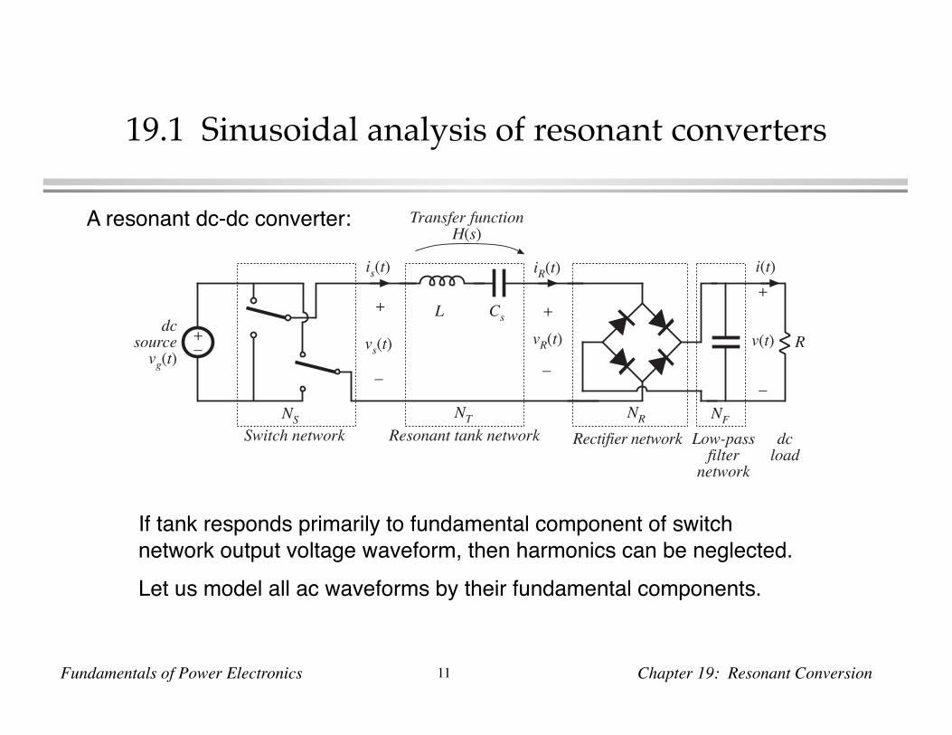
19.1 Sinusoidal analysis of resonant converters
iR(t)
vR(t)
+
–
+–
Transfer functionH(s)
R
+
v(t)
–
Resonant tank network
is(t)
dcsource
vg(t)vs(t)
+
–
Switch network
L Cs
NS NT
i(t)
Rectifier network
NR NF
Low-passfilter
network
dcload
A resonant dc-dc converter:
If tank responds primarily to fundamental component of switch network output voltage waveform, then harmonics can be neglected.
Let us model all ac waveforms by their fundamental components.

Fundamentals of Power Electronics 12 Chapter 19: Resonant Conversion
The sinusoidal approximation
f
Switchoutputvoltage
spectrum
Resonanttank
response
Tankcurrent
spectrum
ffs 3fs 5fs
ffs 3fs 5fs
fs 3fs 5fs
Tank current and output voltage are essentially sinusoids at the switching frequency fs.
Neglect harmonics of switch output voltage waveform, and model only the fundamental component.
Remaining ac waveforms can be found via phasor analysis.

Fundamentals of Power Electronics 13 Chapter 19: Resonant Conversion
19.1.1 Controlled switch network model
is(t)
+–vg vs(t)
+
–
Switch network
NS
1
2
1
2
If the switch network produces a square wave, then its output voltage has the following Fourier series:
vs(t) =4Vg
n = 1, 3, 5,...
1n sin (n st)
The fundamental component is
vs1(t) =4Vg sin ( st) = Vs1 sin ( st)
t
vs(t)
Fundamental componentVg
– Vg
4 Vg
vs1(t)
So model switch network output port with voltage source of value vs1(t)

Fundamentals of Power Electronics 14 Chapter 19: Resonant Conversion
Model of switch network input port
is(t)
+–vg vs(t)
+
–
Switch network
NS
1
2
1
2
st
is(t)
ig(t)
s
Is1
Assume that switch network output current is
is(t) Is1 sin ( st – s)
It is desired to model the dc component (average value) of the switch network input current.
ig(t) Ts= 2Ts
ig( )d0
Ts/2
2Ts
Is1 sin ( s – s)d0
Ts/2
= 2 Is1 cos ( s)

Fundamentals of Power Electronics 15 Chapter 19: Resonant Conversion
Switch network: equivalent circuit
+–
+
vg
–
vs1(t) =4Vg sin ( st)
2Is1 cos ( s)
is1(t) =Is1 sin ( st – s)
• Switch network converts dc to ac
• Dc components of input port waveforms are modeled
• Fundamental ac components of output port waveforms are modeled
• Model is power conservative: predicted average input and output powers are equal

Fundamentals of Power Electronics 16 Chapter 19: Resonant Conversion
19.1.2 Modeling the rectifier and capacitive filter networks
iR(t)
R
+
v(t)
–
i(t)
Rectifier network
NR NF
Low-passfilter
network
dcload
+
vR(t)
–
| iR(t) | vR(t)V
– V
iR(t) st
R
Assume large output filter capacitor, having small ripple.
vR(t) is a square wave, having zero crossings in phase with tank output current iR(t).
If iR(t) is a sinusoid:iR(t) = IR1 sin ( st – R)
Then vR(t) has the following Fourier series:
vR(t) =4V 1
n sin (n st – R)n = 1, 3, 5,

Fundamentals of Power Electronics 17 Chapter 19: Resonant Conversion
Sinusoidal approximation: rectifier
Again, since tank responds only to fundamental components of applied waveforms, harmonics in vR(t) can be neglected. vR(t) becomes
vR1(t) =4V sin ( st – R) = VR1 sin ( st – R)
iR1(t)
vR1(t)fundamental
4 V
iR1(t) =vR1(t)Re
Re =82 R
st
R
vR(t)V
– V
iR(t) st
R
Actual waveforms with harmonics ignored

Fundamentals of Power Electronics 18 Chapter 19: Resonant Conversion
Rectifier dc output port model
iR(t)
R
+
v(t)
–
i(t)
Rectifier network
NR NF
Low-passfilter
network
dcload
+
vR(t)
–
| iR(t) | Output capacitor charge balance: dc load current is equal to average rectified tank output current
iR(t)Ts= I
Hence
I = 2TS
IR1 sin ( st – R) dt0
Ts/2
= 2 IR1vR(t)V
– V
iR(t) st
R

Fundamentals of Power Electronics 19 Chapter 19: Resonant Conversion
Equivalent circuit of rectifier
Rectifier input port:
Fundamental components of current and voltage are sinusoids that are in phase
Hence rectifier presents a resistive load to tank network
Effective resistance Re is
Re =vR1(t)iR(t)
= 82VI
Re =82 R = 0.8106R
With a resistive load R, this becomes
iR1(t)
RRe2 IR1
Re =82 R
+
vR1(t)
–
+
V
–
I
Rectifier equivalent circuit

Fundamentals of Power Electronics 20 Chapter 19: Resonant Conversion
19.1.3 Resonant tank network
Resonantnetwork
is1(t) iR1(t)
Transfer functionH(s)
+–
ReZi
+
vR1(t)
–
vs1(t)
Model of ac waveforms is now reduced to a linear circuit. Tank network is excited by effective sinusoidal voltage (switch network output port), and is load by effective resistive load (rectifier input port).
Can solve for transfer function via conventional linear circuit analysis.

Fundamentals of Power Electronics 21 Chapter 19: Resonant Conversion
Solution of tank network waveforms
Resonantnetwork
is1(t) iR1(t)
Transfer functionH(s)
+–
ReZi
+
vR1(t)
–
vs1(t)
Transfer function:vR1(s)vs1(s)
= H(s)
Ratio of peak values of input and output voltages:
VR1
Vs1= H(s)
s = j s
Solution for tank output current:
iR(s) =vR1(s)Re
=H(s)Re
vs1(s)
which has peak magnitude
IR1 =H(s)
s = j s
ReVs1

Fundamentals of Power Electronics 22 Chapter 19: Resonant Conversion
19.1.4 Solution of convertervoltage conversion ratio M = V/Vg
vs1(t) =4Vg sin ( st)
Resonantnetwork
Transfer functionH(s)
+–
RRe+–
Zi
is1(t) iR1(t)
+
vR1(t)
–
2 IR1
Re =82 R
+
V
–
I
Vg
2Is1 cos ( s)
M = VVg= R 2 1
ReH(s)
s = j s
4
VI
IIR1
IR1VR1
VR1
Vs1
Vs1
Vg
Eliminate Re:
VVg= H(s)
s = j s

Fundamentals of Power Electronics 23 Chapter 19: Resonant Conversion
Conversion ratio M
VVg= H(s)
s = j s
So we have shown that the conversion ratio of a resonant converter, having switch and rectifier networks as in previous slides, is equal to the magnitude of the tank network transfer function. This transfer function is evaluated with the tank loaded by the effective rectifier input resistance Re.

Fundamentals of Power Electronics 24 Chapter 19: Resonant Conversion
19.2 Examples19.2.1 Series resonant converter
iR(t)
vR(t)
+
–
+–
transfer functionH(s)
R
+
v(t)
–
resonant tank network
is(t)
dcsource
vg(t)vs(t)
+
–
switch network
L Cs
NS NT
i(t)
rectifier network
NR NF
low-passfilter
network
dcload

Fundamentals of Power Electronics 25 Chapter 19: Resonant Conversion
Model: series resonant converter
series tank network
L C
vs1(t) =4Vg sin ( st)
transfer function H(s)
+–
ReZi
is1(t) iR1(t)
+
vR1(t)
–
Re =82 R
+–Vg
2Is1 cos ( s)
R2 IR1
+
V
–
I
H(s) =Re
Zi(s)=
Re
Re + sL +1sC
=
sQe 0
1 + sQe 0
+ s0
2
0 =1LC
= 2 f0
R0 =LC
Qe =R0Re
M = H( j s) =1
1 + Qe2 1F– F
2

Fundamentals of Power Electronics 26 Chapter 19: Resonant Conversion
Construction of Zi
1C
Re
|| Zi ||
f0
L
R0
Qe = R0 / Re

Fundamentals of Power Electronics 27 Chapter 19: Resonant Conversion
Construction of H
1|| H ||
f0
Qe = Re / R0
Re / R0
R eC
Re / L

Fundamentals of Power Electronics 28 Chapter 19: Resonant Conversion
19.2.2 Subharmonic modes of the SRC
f
switchoutputvoltage
spectrum
resonanttank
response
tankcurrent
spectrum
ffs 3fs 5fs
ffs 3fs 5fs
fs 3fs 5fs
Example: excitation of tank by third harmonic of switching frequency
Can now approximate vs(t) by its third harmonic:
vs(t) vsn(t) =4Vg
n sin (n st)
Result of analysis:
M = VVg=
H( jn s)n

Fundamentals of Power Electronics 29 Chapter 19: Resonant Conversion
Subharmonic modes of SRC
fsf0
M
etc.13 f0
15 f0
1315
1

Fundamentals of Power Electronics 30 Chapter 19: Resonant Conversion
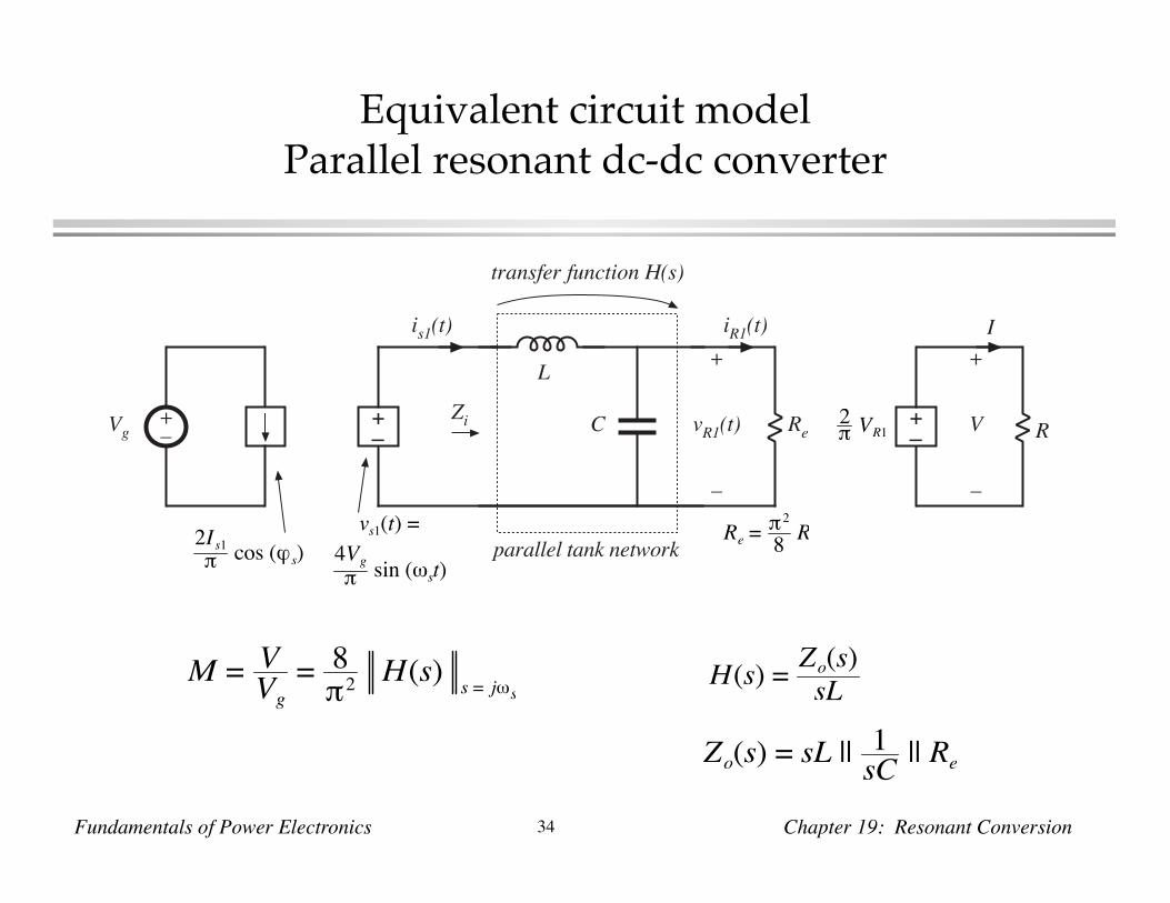
19.2.3 Parallel resonant dc-dc converter
iR(t)
vR(t)
+
–
+– R
+
v(t)
–
resonant tank network
is(t)
dcsource
vg(t)vs(t)
+
–
switch network
L
Cp
NS NT
i(t)
rectifier network
NR NF
low-pass filternetwork
dcload
Differs from series resonant converter as follows:
Different tank network
Rectifier is driven by sinusoidal voltage, and is connected to inductive-input low-pass filter
Need a new model for rectifier and filter networks

Fundamentals of Power Electronics 31 Chapter 19: Resonant Conversion
Model of uncontrolled rectifierwith inductive filter network
vR(t)
I
– I
iR(t)
st
R
vR1(t)
iR1(t)fundamental
4 I
iR1(t) =vR1(t)Re
Re =2
8R
st
R
iR(t)
vR(t)
+
–
R
+
v(t)
–
k
i(t)
rectifier network
NR NF
low-pass filternetwork
dcload
Fundamental component of iR(t):
iR1(t) =4I sin ( st – R)

Fundamentals of Power Electronics 32 Chapter 19: Resonant Conversion
Effective resistance Re
Re =vR1(t)iR1(t)
=VR1
4I
Again define
In steady state, the dc output voltage V is equal to the average value of | vR |:
V = 2TSVR1 sin ( st – R) dt
0
Ts/2
= 2 VR1
For a resistive load, V = IR. The effective resistance Re can then be expressed
Re =2
8R = 1.2337R

Fundamentals of Power Electronics 33 Chapter 19: Resonant Conversion
Equivalent circuit model of uncontrolled rectifierwith inductive filter network
iR1(t)
RRe
Re =2
8R
+
vR1(t)
–
+
V
–
I
+–
2 VR1
Fundamentals of Power Electronics 34 Chapter 19: Resonant Conversion
Equivalent circuit modelParallel resonant dc-dc converter
parallel tank network
L
C
vs1(t) =4Vg sin ( st)
transfer function H(s)
+–
ReZi
is1(t) iR1(t)
+
vR1(t)
–
+–Vg
2Is1 cos ( s)Re =
2
8R
R
+
V
–
I
+–
2 VR1
M = VVg= 8
2 H(s)s = j s
H(s) =Zo(s)sL
Zo(s) = sL ||1sC|| Re

Fundamentals of Power Electronics 35 Chapter 19: Resonant Conversion
Construction of Zo
1C
Re
|| Zo ||
f0
L
R0
Qe = Re / R0

Fundamentals of Power Electronics 36 Chapter 19: Resonant Conversion
Construction of H
12LC
1
|| H ||
f0
Qe = Re / R0
Re / R0

Fundamentals of Power Electronics 37 Chapter 19: Resonant Conversion
Dc conversion ratio of the PRC
M = 82
Zo(s)sL s = j s
= 82
11 + s
Qe 0+ s
0
2
s = j s
= 82
1
1 – F 2 2+ F
Qe
2
M = 82
Re
R0= RR0
At resonance, this becomes
• PRC can step up the voltage, provided R > R0
• PRC can produce M approaching infinity, provided output current is limited to value less than Vg / R0

Fundamentals of Power Electronics 57 Chapter 19: Resonant Conversion
19.4.1 Operation of the full bridge below resonance: Zero-current switching
Series resonant converter example
L
+–Vg
CQ1
Q2
Q3
Q4
D1
D2
D3
D4
+
vs(t)
– is(t)
+
vds1(t)
–iQ1(t)
Operation below resonance: input tank current leads voltage
Zero-current switching (ZCS) occurs

Fundamentals of Power Electronics 58 Chapter 19: Resonant Conversion
Tank input impedance
1C
Re
|| Zi ||
f0
L
R0
Qe = R0 /Re
Operation below resonance: tank input impedance Zi is dominated by tank capacitor.
∠Zi is positive, and tank input current leads tank input voltage.
Zero crossing of the tank input current waveform is(t) occurs before the zero crossing of the voltage vs(t).

Fundamentals of Power Electronics 59 Chapter 19: Resonant Conversion
Switch network waveforms, below resonanceZero-current switching
Ts
2
t
vs(t)
Vg
– Vg
vs1(t)
t
is(t)
t
Ts
2+ t
Q1
Q4
D1
D4
Q2
Q3
D2
D3
Conductingdevices:
“Hard”turn-on of
Q1, Q4
“Soft”turn-off of
Q1, Q4
“Hard”turn-on of
Q2, Q3
“Soft”turn-off of
Q2, Q3
L CQ1
Q2
Q3
Q4
D1
D2
D3
D4
+
vs(t)
– is(t)
+
vds1(t)
–iQ1(t)
Conduction sequence: Q1–D1–Q2–D2
Q1 is turned off during D1 conduction interval, without loss
Fundamentals of Power Electronics 60 Chapter 19: Resonant Conversion
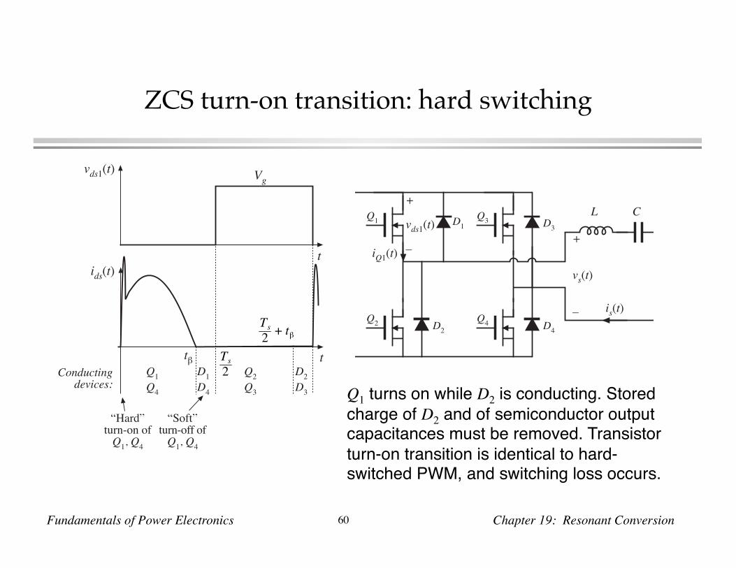
ZCS turn-on transition: hard switching
L CQ1
Q2
Q3
Q4
D1
D2
D3
D4
+
vs(t)
– is(t)
+
vds1(t)
–iQ1(t)
Q1 turns on while D2 is conducting. Stored charge of D2 and of semiconductor output capacitances must be removed. Transistor turn-on transition is identical to hard-switched PWM, and switching loss occurs.
Ts2
t
ids(t)
t
Ts2
+ t
Q1
Q4
D1
D4
Q2
Q3
D2
D3
Conductingdevices:
“Hard”turn-on ofQ1, Q4
“Soft”turn-off ofQ1, Q4
t
Vgvds1(t)

Fundamentals of Power Electronics 61 Chapter 19: Resonant Conversion
19.4.2 Operation of the full bridge above resonance: Zero-voltage switching
Series resonant converter example
L
+–Vg
CQ1
Q2
Q3
Q4
D1
D2
D3
D4
+
vs(t)
– is(t)
+
vds1(t)
–iQ1(t)
Operation above resonance: input tank current lags voltage
Zero-voltage switching (ZVS) occurs

Fundamentals of Power Electronics 62 Chapter 19: Resonant Conversion
Tank input impedance
1C
Re
|| Zi ||
f0
L
R0
Qe = R0 /Re
Operation above resonance: tank input impedance Zi is dominated by tank inductor.
∠Zi is negative, and tank input current lags tank input voltage.
Zero crossing of the tank input current waveform is(t) occurs after the zero crossing of the voltage vs(t).

Fundamentals of Power Electronics 63 Chapter 19: Resonant Conversion
Switch network waveforms, above resonanceZero-voltage switching
L CQ1
Q2
Q3
Q4
D1
D2
D3
D4
+
vs(t)
– is(t)
+
vds1(t)
–iQ1(t)
Conduction sequence: D1–Q1–D2–Q2
Q1 is turned on during D1 conduction interval, without loss

Fundamentals of Power Electronics 64 Chapter 19: Resonant Conversion
ZVS turn-off transition: hard switching?
L CQ1
Q2
Q3
Q4
D1
D2
D3
D4
+
vs(t)
– is(t)
+
vds1(t)
–iQ1(t)
When Q1 turns off, D2 must begin conducting. Voltage across Q1 must increase to Vg. Transistor turn-off transition is identical to hard-switched PWM. Switching loss may occur (but see next slide).

Fundamentals of Power Electronics 65 Chapter 19: Resonant Conversion
Soft switching at the ZVS turn-off transition
• Introduce small capacitors Cleg across each device (or use device output capacitances).
• Introduce delay between turn-off of Q1 and turn-on of Q2.
Tank current is(t) charges and discharges Cleg. Turn-off transition becomes lossless. During commutation interval, no devices conduct.
So zero-voltage switching exhibits low switching loss: losses due to diode stored charge and device output capacitances are eliminated.

Fundamentals of Power Electronics 12 Chapter 19: Resonant Conversion
19.4 Load-dependent properties of resonant converters
Resonant inverter design objectives:
1. Operate with a specified load characteristic and range of operating points• With a nonlinear load, must properly match inverter output
characteristic to load characteristic2. Obtain zero-voltage switching or zero-current switching
• Preferably, obtain these properties at all loads• Could allow ZVS property to be lost at light load, if necessary
3. Minimize transistor currents and conduction losses• To obtain good efficiency at light load, the transistor current should
scale proportionally to load current (in resonant converters, it often doesnʼt!)

Fundamentals of Power Electronics 69 Chapter 19: Resonant Conversion
Inverter output characteristics
Let H∞ be the open-circuit (R ∞) transfer function:
and let Zo0 be the output impedance (with vi short-circuit). Then,
The output voltage magnitude is:
with
This result can be rearranged to obtain
Hence, at a given frequency, the output characteristic (i.e., the relationship between || v || and || i ||) of any resonant inverter of this class is elliptical.
H (s) =v(s)vs1(s) R
v(s) = H (s)vs1(s)R
R + Zo0(s)
R =v( j s)
i( j s)
v( j s)2=
H ( j s)2vs( j s)
2
1 +Zo0( j s)
2
R2
v( j s)2+ i( j s)
2Zo0( j s)
2= H ( j s)
2vs( j s)
2

Fundamentals of Power Electronics 70 Chapter 19: Resonant Conversion
Inverter output characteristics
General resonant inverter output characteristics are elliptical, of the form
This result is valid provided that (i) the resonant network is purely reactive, and (ii) the load is purely resistive.
i
v Voc
2
Matched lo
ad
R = Z o0
Isc
2
Inverter outputcharacteristic
Voc = H vs
Isc =H vs
Zo0
v( j s)2
V oc2 +
i( j s)2
I sc2 = 1
Voc = H ( j s) vs( j s)
I sc =H ( j s) vs( j s)
Zo0( j s)=
VocZo0( j s)
with

Fundamentals of Power Electronics 16 Chapter 19: Resonant Conversion
Matching ellipse to application requirements
|| vo ||
|| io ||
inverter characteristic
lamp characteristic
Electronic ballast Electrosurgical generator
|| vo ||
|| io ||
inverter characteristic
50
matched load
400W
2A
2kV

Fundamentals of Power Electronics 17 Chapter 19: Resonant Conversion
Input impedance of the resonant tank network
Zi(s) = Zi0(s)
1 + RZo0(s)
1 + RZo (s)
= Zi (s)
1 +Zo0(s)
R
1 +Zo (s)
Rvs1(t)
EffectiveresistiveloadR
is(t) i(t)
v(t)
+
–
Zi Zo
Transfer functionH(s)
+–
Effectivesinusoidal
sourceResonantnetwork
Purely reactive
where
Zi0 =viii R 0
Zi =viii R
Zo0 =vo– io vi short circuit
Zo =vo– io vi open circuit

Fundamentals of Power Electronics 19 Chapter 19: Resonant Conversion
Zi0 and Zi∞ for 3 common inverters
Series
Parallel
LCC
f
L
1C
s+ 1
Cp
1C
s
|| Zi0 ||
|| Zi ||
f
L
1C
p
|| Zi0 ||
|| Zi ||
f
L
1C
s
|| Zi0 ||
|| Zi ||
Zo
CsL
Zi
ZoCp
L
Zi
Zo
Cs
Cp
L
Zi
Zi0(s) = sL +1sCs
Zi (s) =
Zi0(s) = sL
Zi (s) = sL +1sCp
Zi0(s) = sL +1sCs
Zi (s) = sL +1sCp
+ 1sCs

Fundamentals of Power Electronics 18 Chapter 19: Resonant Conversion
Other relations
H(s) =H (s)
1 + RZo0
Zi0
Zi
=Zo0
Zo
H2= Zo0
1Zi0– 1Zi
H =vo(s)vi(s) R
Reciprocity
Tank transfer function
where
If the tank network is purely reactive, then each of its impedances and transfer functions have zero real parts:
Zi
2= ZiZ i
* = Zi02
1 + R2
Zo0
2
1 + R2
Zo
2
Hence, the input impedance magnitude is
Zi0 = – Z i0*
Zi = – Z i*
Zo0 = – Zo0*
Zo = – Zo*
H = – H *

Fundamentals of Power Electronics 20 Chapter 19: Resonant Conversion
A Theorem relating transistor current variations to load resistance R
Theorem 1: If the tank network is purely reactive, then its input impedance || Zi || is a monotonic function of the load resistance R.
So as the load resistance R varies from 0 to ∞, the resonant network input impedance || Zi || varies monotonically from the short-circuit value || Zi0 || to the open-circuit value || Zi∞ ||.
The impedances || Zi∞ || and || Zi0 || are easy to construct. If you want to minimize the circulating tank currents at light load,
maximize || Zi∞ ||.
Note: for many inverters, || Zi∞ || < || Zi0 || ! The no-load transistor current is therefore greater than the short-circuit transistor current.

Fundamentals of Power Electronics 21 Chapter 19: Resonant Conversion
Proof of Theorem 1
Zi
2= Zi0
2
1 + RZo0
2
1 + RZo
2
d Zi
2
d R= 2 Zi0
2
1Zo0
2 –1Zo
2 R
1 + R2
Zo
2
2
Derivative has roots at:
(i) R = 0(ii) R =
(iii) Zo0 = Zo , or Zi0 = Zi
Previously shown: Differentiate:
So the resonant network input impedance is a monotonic function of R, over the range 0 < R < ∞.
In the special case || Zi0 || = || Zi∞ ||,|| Zi || is independent of R.

Fundamentals of Power Electronics 22 Chapter 19: Resonant Conversion
Example: || Zi || of LCC
• for f < f m, || Zi || increases with increasing R .
• for f > f m, || Zi || decreases with increasing R .
• at a given frequency f, || Zi || is a monotonic function of R.
• Itʼs not necessary to draw the entire plot: just construct || Zi0 || and || Zi∞ ||.
f
|| Zi || ff
incr
easi
ng R L
fm
1C
s+ 1
Cp
1C
s
increasing R

Fundamentals of Power Electronics 23 Chapter 19: Resonant Conversion
Discussion: LCC
|| Zi0 || and || Zi∞ || both represent series resonant impedances, whose Bode diagrams are easily constructed.
|| Zi0 || and || Zi∞ || intersect at frequency fm.
For f < fm
then || Zi0 || < || Zi∞ || ; hence transistor current decreases as load current decreases
For f > fm
then || Zi0 || > || Zi∞ || ; hence transistor current increases as load current decreases, and transistor current is greater than or equal to short-circuit current for all R
f
|| Zi ||
L
fm
1C
s+ 1
Cp
1C
s
|| Zi0 |||| Zi ||
f0 =1
2 LCs
f = 12 LCs||Cp
fm =1
2 LCs||2C p
f0 f
L Cs
CpZi
L Cs
CpZi0
LCC example

Fundamentals of Power Electronics 24 Chapter 19: Resonant Conversion
Discussion -series and parallel
Series
Parallel
LCC
f
L
1C
s+ 1
Cp
1C
s
|| Zi0 ||
|| Zi ||
f
L
1C
p
|| Zi0 ||
|| Zi ||
f
L
1C
s
|| Zi0 ||
|| Zi ||
Zo
CsL
Zi
ZoCp
L
Zi
Zo
Cs
Cp
L
Zi
• No-load transistor current = 0, both above and below resonance.
• ZCS below resonance, ZVS above resonance
• Above resonance: no-load transistor current is greater than short-circuit transistor current. ZVS.
• Below resonance: no-load transistor current is less than short-circuit current (for f <fm), but determined by || Zi∞ ||. ZCS.

Fundamentals of Power Electronics 25 Chapter 19: Resonant Conversion
A Theorem relating the ZVS/ZCS boundary to load resistance R
Theorem 2: If the tank network is purely reactive, then the boundary between zero-current switching and zero-voltage switching occurs when the load resistance R is equal to the critical value Rcrit, given by
Rcrit = Zo0
– Zi
Zi0
It is assumed that zero-current switching (ZCS) occurs when the tank input impedance is capacitive in nature, while zero-voltage switching (ZVS) occurs when the tank is inductive in nature. This assumption gives a necessary but not sufficient condition for ZVS when significant semiconductor output capacitance is present.

Fundamentals of Power Electronics 26 Chapter 19: Resonant Conversion
Im Zi(Rcrit) = Im Zi Re
1 +Zo0
Rcrit
1 +Zo
Rcrit
= Im Zi Re
1 –Zo0Zo
Rcrit2
1 +Zo
2
Rcrit2
Proof of Theorem 2
Previously shown:
Zi = Zi
1 +Zo0
R
1 +Zo
R
If ZCS occurs when Zi is capacitive, while ZVS occurs when Zi is inductive, then the boundary is determined by ∠Zi = 0. Hence, the critical load Rcrit is the resistance which causes the imaginary part of Zi to be zero:
Im Zi(Rcrit) = 0
Note that Zi∞, Zo0, and Zo∞ have zero real parts. Hence,
Solution for Rcrit yields
Rcrit = Zo0
– Zi
Zi0

Fundamentals of Power Electronics 27 Chapter 19: Resonant Conversion
Discussion —Theorem 2
Rcrit = Zo0
– Zi
Zi0
Again, Zi∞, Zi0, and Zo0 are pure imaginary quantities.
If Zi∞ and Zi0 have the same phase (both inductive or both capacitive), then there is no real solution for Rcrit.
Hence, if at a given frequency Zi∞ and Zi0 are both capacitive, then ZCS occurs for all loads. If Zi∞ and Zi0 are both inductive, then ZVS occurs for all loads.
If Zi∞ and Zi0 have opposite phase (one is capacitive and the other is inductive), then there is a real solution for Rcrit. The boundary between ZVS and ZCS operation is then given by R = Rcrit.
Note that R = || Zo0 || corresponds to operation at matched load with maximum output power. The boundary is expressed in terms of this matched load impedance, and the ratio Zi∞ / Zi0.

Fundamentals of Power Electronics 28 Chapter 19: Resonant Conversion
LCC example
Rcrit = Zo0
– Zi
Zi0
f
|| Zi ||
L
f1
1C
s+ 1
Cp
1C
s|| Zi0 ||
|| Zi ||
f0 f
ZVSfor all R
ZCSfor all R
ZCS: R>Rcrit
ZVS: R<Rcrit
{Zi
Zi0
fm
For f > f∞, ZVS occurs for all R.
For f < f0, ZCS occurs for all R. For f0 < f < f∞, ZVS occurs for
R< Rcrit, and ZCS occurs for R> Rcrit.
Note that R = || Zo0 || corresponds to operation at matched load with maximum output power. The boundary is expressed in terms of this matched load impedance, and the ratio Zi∞ / Zi0.
Fundamentals of Power Electronics 29 Chapter 19: Resonant Conversion
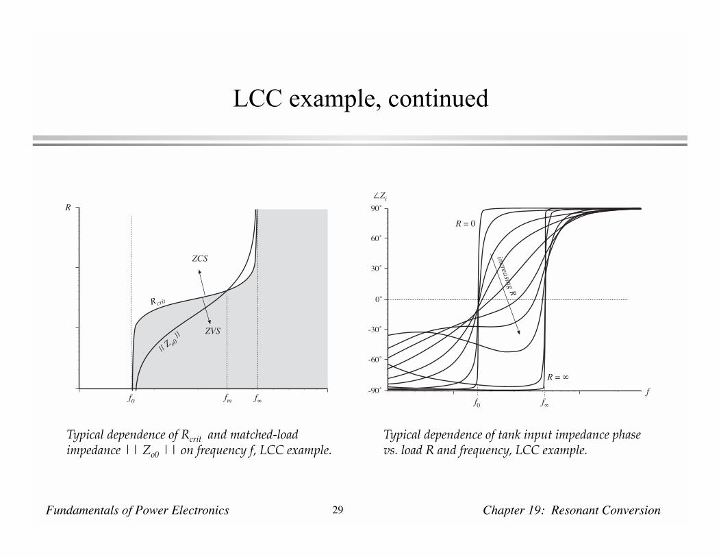
LCC example, continued
Rcrit
|| Zo0 ||
f0 ffm
ZCS
ZVS
R
Typical dependence of Rcrit and matched-load impedance || Zo0 || on frequency f, LCC example.
Typical dependence of tank input impedance phase vs. load R and frequency, LCC example.
-90˚
-60˚
-30˚
0˚
30˚
60˚
90˚
ff0
R =
R = 0increasing R
f
Zi

A popular subclass of tank circuits
jXs
jXp
Tank network
H ( ) =Xp
Xp + Xs
Zo0( ) =jXsXp
Xp + Xs= jXsH ( )
Ma
2
+ Jb
2
= 1 (output characteristic)
M = 1
1a2+
Qe
b
2(control characteristic)
a = H ( ) =Xp
Xp + Xs
b =H ( ) Ro
Zo0( )=
Ro
Xs
M =Vout
Vin, J =
IoutRo
Vin, Qe =
Ro
Re
Zi0 = jXs, Zi = j Xs + Xp
At f = fm: Xs = –12 Xp
Key equations
Tank Series branch reactance Xs Shunt branch reactance Xp
Series L – 1C
Parallel L – 1C
LCC L – 1Cs
– 1Cp
LLC Ls –1C
Lp
Rcrit = Zo0 –Zi
Zi0= Xp –
Xs
Xs + Xp

Important frequencies of popular tank circuits
Tank 0 m
Series 1LC
Parallel 1LC
12LC
LCC 1LCs
1LCs Cp
1LCs 2Cp
LLC 1LsC
1Ls + L p C
1
Ls +L p
2C

The LLC tank network
Zi0 = sLs + 1/sC Zi∞ = s(Ls + Lp) + 1/sC
DC-DC converter circuit
Tank network input impedances

LLC Tank input impedance plots Zi0, Zi∞
Good characteristics obtained for fs > fm• Switch current
varies directly with load current
• ZVS obtained at most operating points including matched load

LLC output characteristic for fm < fs < f0
Rcrit < || Zo0 || so ZVS region includes matched load

LLC: ZVS boundary in the region f0 < fs < f∞
n = 4Rcrit
Ro0= nF
1 + n
1 – F 2
1 + nF 2 – 1
Ro0 =Ls
C
n =L p
Ls
F =fsf ZVS for R > Rcrit
ZCS for R < Rcrit
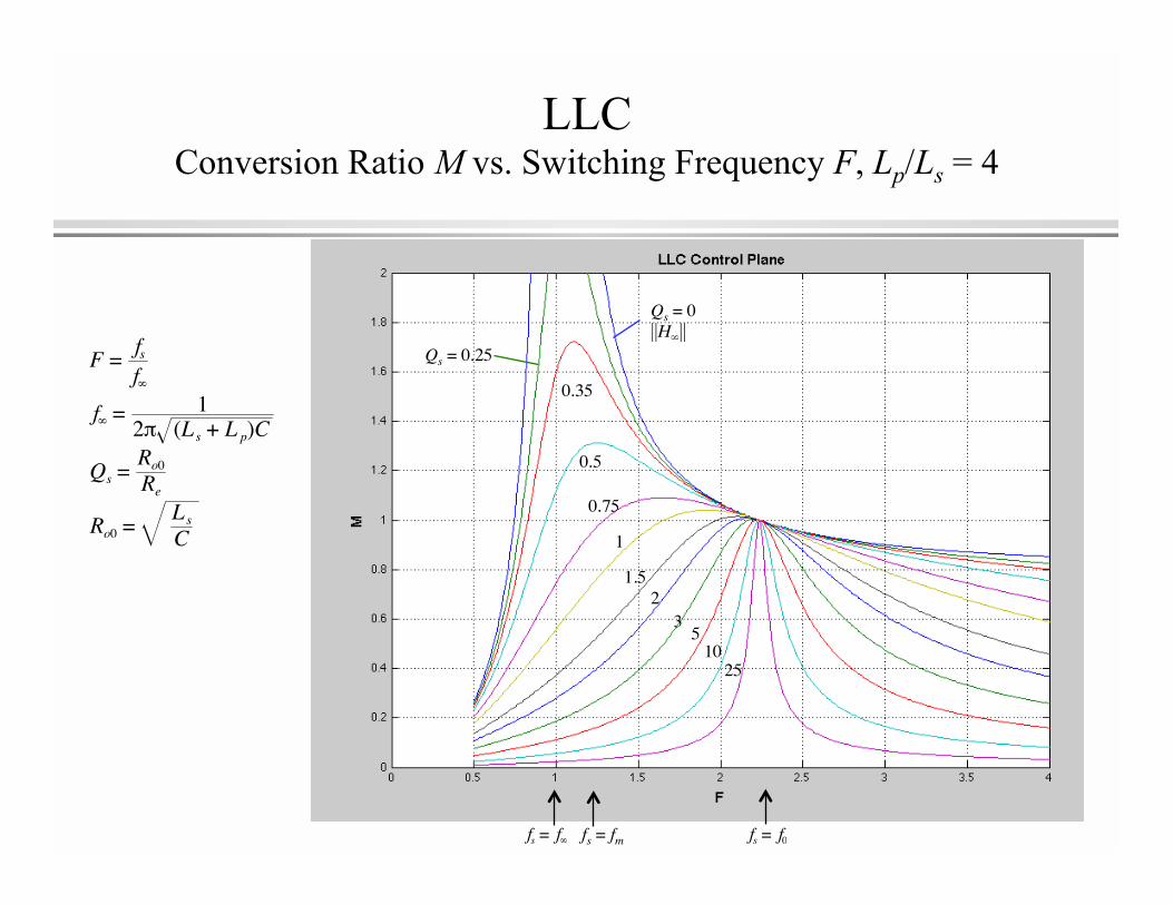
LLC Conversion Ratio M vs. Switching Frequency F, Lp/Ls = 4
Qs = 0||H∞||
Qs = 0.25
0.35
0.5
1
0.75
1.52
35
1025
fs = f fs = f0
F =fsf
f = 12 (Ls + L p)C
Qs =Ro0
Re
Ro0 =Ls
C
fs = fm

LLC Output plane characteristic, Lp/Ls = 4
F = 1
F = 0.5
Increasing FF = 1
F = 1 + n
Increasing F
F = 1 + n
Increasing F
F = 10
fs < f∞ f∞ < fs < f0
f0 < fsF =
fsf
f = 12 (Ls + L p)C
f0 =1
2 LsCf0 = 1 + n f
n =L p
Ls
M = VVg
J =IRo0
Vg
fm = f1 + n1 + n
2

Summary
1. Simple models approximate the tank waveforms by their fundamental sinusoidal components, and that facilitate resonant converter design using conventional frequency response methods
2. Several theorems show how to employ frequency response plots to determine important properties:• The inverter or dc-dc converter elliptical output characteristic• How the transistor currents vary with load, and how to shape the
tank impedances to improve light-load efficiency
• Dependence of the ZVS/ZCS boundary on load3. The LLC tank network exhibits the following advantages:
• Buck-boost conversion ratio• Wide range of operating points exhibiting zero-voltage switching,
i.e., for f0 < fs or for f∞ < fs < f0 with Re > Rcrit• Transistor currents vary directly with load current for fm < fs

Selected References
1. R. L. Steigerwald, “A Comparison of Half-Bridge Resonant Converter Topologies,” IEEE APEC, 1987 Record, pp. 135-144.
2. S. Johnson, “Steady-State Analysis and Design of the Parallel Resonant Converter,” M.S. Thesis, Univ. of Colo., 1986.
3. R. Erickson and D. Maksimovic, Fundamentals of Power Electronics, 2nd ed., Chapter 19, Springer, 2001.
4. B. Yang, F. Lee, A. Zhang, and G. Huang, “LLC Resonant Converter for Front-End DC/DC Conversion,” IEEE APEC, 2002 Record, pp. 1108-1112.